technical note 5: digital double-correlated sampler: a ...qucam.com/assets/tn5.pdf · 6 qucam tn5...
TRANSCRIPT
Technical Note 5:
Digital Double-Correlated Sampler: A PracticalImplementation
Simon Tulloch
QUCAM
Cadiz
Spain
December 27th 2015
1
Contents
1 Introduction 4
1.1 DCDS testbed controller . . . . . . . . . . . . . . . . . . . . . . . . . 4
2 Detailed Hardware Description 5
2.1 Power supply . . . . . . . . . . . . . . . . . . . . . . . . . . . . . . . 5
2.2 Video preamplifier . . . . . . . . . . . . . . . . . . . . . . . . . . . . 6
2.3 Bias generators . . . . . . . . . . . . . . . . . . . . . . . . . . . . . . 8
2.4 Clock drivers . . . . . . . . . . . . . . . . . . . . . . . . . . . . . . . 8
2.5 FPGA module . . . . . . . . . . . . . . . . . . . . . . . . . . . . . . . 8
2.6 VHDL-defined circuitry . . . . . . . . . . . . . . . . . . . . . . . . . . 8
2.7 FPGA resource utilisation . . . . . . . . . . . . . . . . . . . . . . . . 10
2.8 The ADC . . . . . . . . . . . . . . . . . . . . . . . . . . . . . . . . . 10
3 Video amplifier characterisation 11
3.1 Measurement of gain and bandwidth . . . . . . . . . . . . . . . . . . 11
3.2 Amplifier noise floor . . . . . . . . . . . . . . . . . . . . . . . . . . . 13
4 Initial imaging tests 13
5 Measurement of CCD231 Noise Spectrum 14
5.1 Calibration of Spectrum Analyser . . . . . . . . . . . . . . . . . . . . 14
5.2 Noise Spectrum result . . . . . . . . . . . . . . . . . . . . . . . . . . 17
5.3 Comparison with the E2V noise model . . . . . . . . . . . . . . . . . 20
6 Video waveform processing technique 20
6.1 The differential averager . . . . . . . . . . . . . . . . . . . . . . . . . 20
6.2 The video processor transfer function . . . . . . . . . . . . . . . . . . 20
6.3 Relationship between transfer function and CCD read noise . . . . . . 22
6.4 Implementation of a Digital CDS . . . . . . . . . . . . . . . . . . . . 23
2
7 In-depth imaging characterisation 24
7.1 Photon transfer gain measurement. . . . . . . . . . . . . . . . . . . . 24
7.2 Effect of constant current load on CCD noise. . . . . . . . . . . . . . 26
8 DCDS noise results 28
8.1 Effect of ADC frequency . . . . . . . . . . . . . . . . . . . . . . . . . 28
8.2 Shortcomings and future work . . . . . . . . . . . . . . . . . . . . . . 29
3
4 QUCAM TN5
1 Introduction
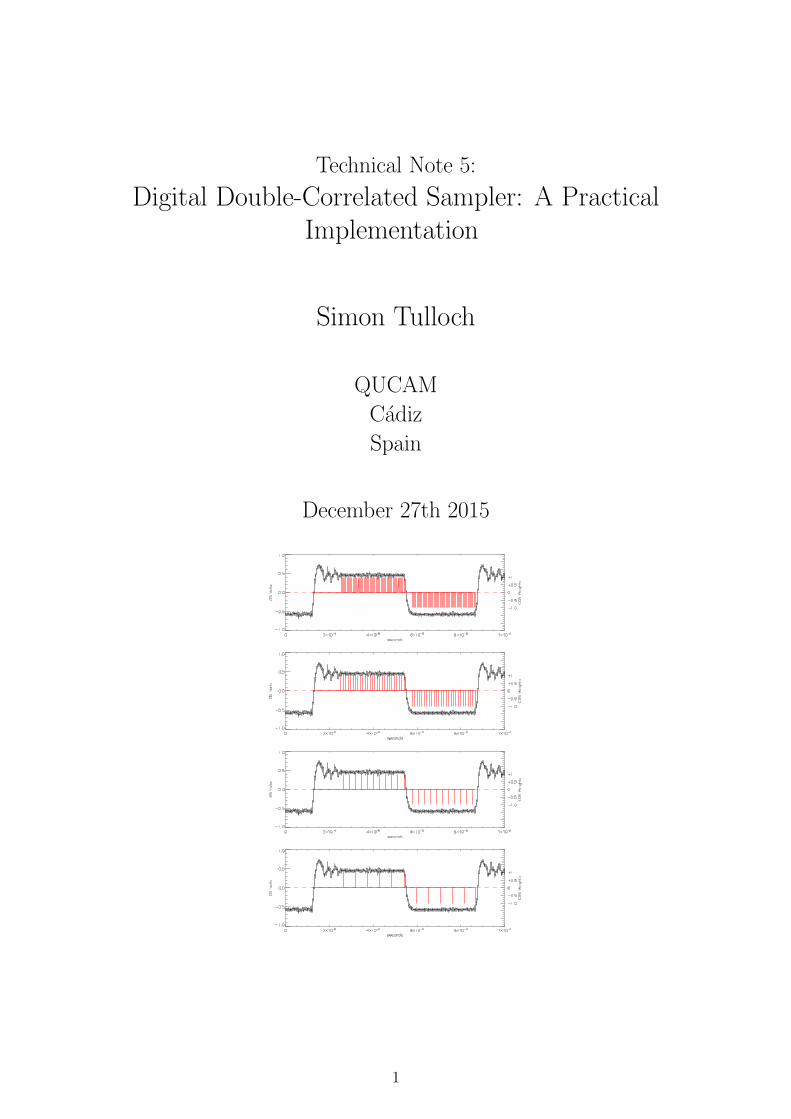
Modern scientific CCDs are capable of giving extremely low read noise in the regionof 2 to 3 e−. To reach this noise floor requires the use of an extremely well designedvideo processor, traditionally implemented using analogue circuitry, coupled to ahigh-resolution analogue to digital converter (ADC). The video waveform providedby the CCD (see Figure 1) requires two measurements for each pixel, one just afterthe CCD output transistor has been reset and another just after the pixel chargehas been dumped onto the measurement node. The difference between these twopedestal measurements then gives the pixel value proportional to the photo-chargepresent. Since two measurements are used, the technique is known as CorrelatedDouble Sampling or CDS. In recent years a number of papers have been publishedexploring the advantages of using purely digital techniques to process the waveform.Digital CDS (DCDS) still requires a conventional analogue front end amplifier butdoes most of the processing in the digital domain. This reduces complexity aswell as offering the possibility of using digital filtering techniques to give higherperformance. This study describes the design and operation of a practical DCDStest-bed system used with an E2V CCD231 4kx4k CCD.
Figure 1: An oscilloscope capture of an E2V CCD231 video waveform overapproximately 1.5 pixel periods. The oscilloscope probe was attached di-rectly to the OS line of the CCD. Key parts of the waveform are labeled.
1.1 DCDS testbed controller
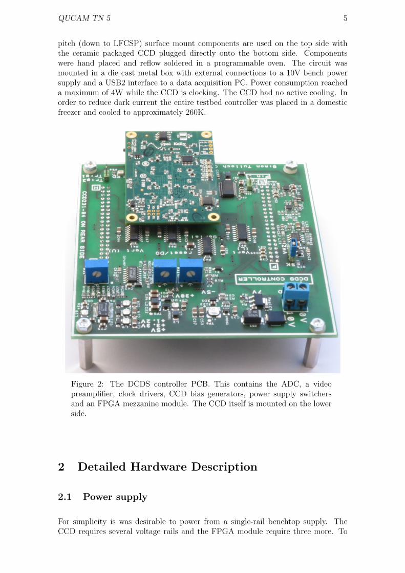
This controller was initially conceived of as a spectrum analyser for measuring thenoise on the output transistor of a CCD231. It was then realised that with a smallamount of additional circuitry it could function as a complete single channel CCDcontroller. It is implemented on a double sided PCB measuring 10x10cm. Fine
QUCAM TN 5 5
pitch (down to LFCSP) surface mount components are used on the top side withthe ceramic packaged CCD plugged directly onto the bottom side. Componentswere hand placed and reflow soldered in a programmable oven. The circuit wasmounted in a die cast metal box with external connections to a 10V bench powersupply and a USB2 interface to a data acquisition PC. Power consumption reacheda maximum of 4W while the CCD is clocking. The CCD had no active cooling. Inorder to reduce dark current the entire testbed controller was placed in a domesticfreezer and cooled to approximately 260K.
Figure 2: The DCDS controller PCB. This contains the ADC, a videopreamplifier, clock drivers, CCD bias generators, power supply switchersand an FPGA mezzanine module. The CCD itself is mounted on the lowerside.
2 Detailed Hardware Description
2.1 Power supply
For simplicity is was desirable to power from a single-rail benchtop supply. TheCCD requires several voltage rails and the FPGA module require three more. To
6 QUCAM TN5
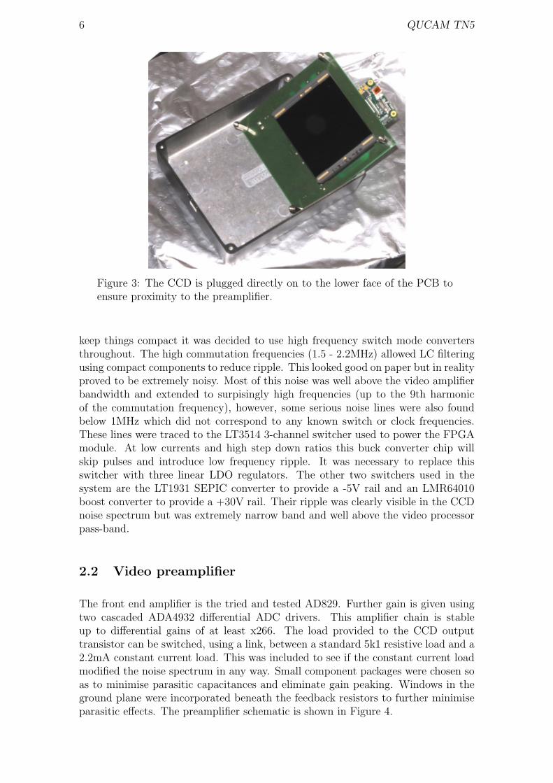
Figure 3: The CCD is plugged directly on to the lower face of the PCB toensure proximity to the preamplifier.
keep things compact it was decided to use high frequency switch mode convertersthroughout. The high commutation frequencies (1.5 - 2.2MHz) allowed LC filteringusing compact components to reduce ripple. This looked good on paper but in realityproved to be extremely noisy. Most of this noise was well above the video amplifierbandwidth and extended to surpisingly high frequencies (up to the 9th harmonicof the commutation frequency), however, some serious noise lines were also foundbelow 1MHz which did not correspond to any known switch or clock frequencies.These lines were traced to the LT3514 3-channel switcher used to power the FPGAmodule. At low currents and high step down ratios this buck converter chip willskip pulses and introduce low frequency ripple. It was necessary to replace thisswitcher with three linear LDO regulators. The other two switchers used in thesystem are the LT1931 SEPIC converter to provide a -5V rail and an LMR64010boost converter to provide a +30V rail. Their ripple was clearly visible in the CCDnoise spectrum but was extremely narrow band and well above the video processorpass-band.
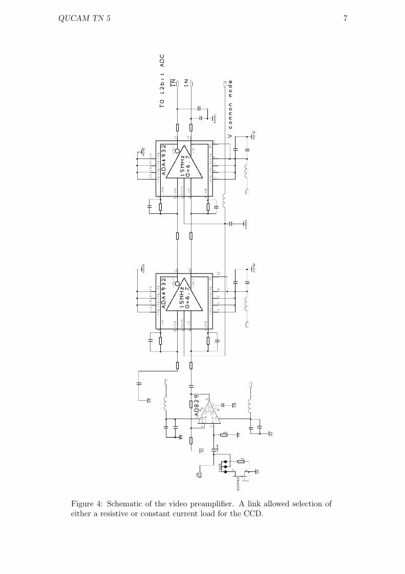
2.2 Video preamplifier
The front end amplifier is the tried and tested AD829. Further gain is given usingtwo cascaded ADA4932 differential ADC drivers. This amplifier chain is stableup to differential gains of at least x266. The load provided to the CCD outputtransistor can be switched, using a link, between a standard 5k1 resistive load and a2.2mA constant current load. This was included to see if the constant current loadmodified the noise spectrum in any way. Small component packages were chosen soas to minimise parasitic capacitances and eliminate gain peaking. Windows in theground plane were incorporated beneath the feedback resistors to further minimiseparasitic effects. The preamplifier schematic is shown in Figure 4.
QUCAM TN 5 7
Figure 4: Schematic of the video preamplifier. A link allowed selection ofeither a resistive or constant current load for the CCD.
8 QUCAM TN5
2.3 Bias generators
Biases to the CCD are provided by a high voltage rail-to-rail quad op-amp. Thebias voltages were trimmed manually using potentiometers.
2.4 Clock drivers
A total of 9 clocks are required to image the CCD. These are provided by fourEL7457 pin-driver ICs. Clock levels were hard wired and not programmable.
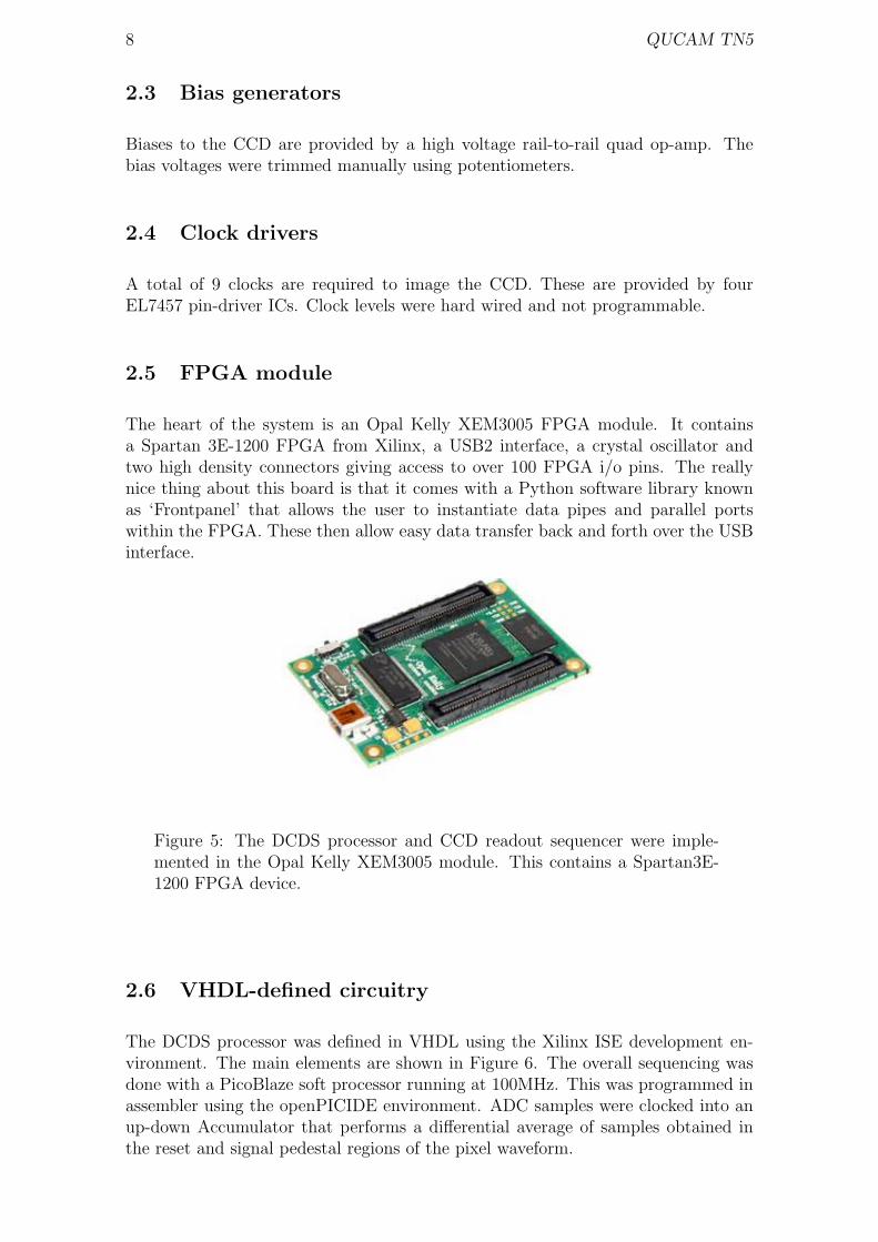
2.5 FPGA module
The heart of the system is an Opal Kelly XEM3005 FPGA module. It containsa Spartan 3E-1200 FPGA from Xilinx, a USB2 interface, a crystal oscillator andtwo high density connectors giving access to over 100 FPGA i/o pins. The reallynice thing about this board is that it comes with a Python software library knownas ‘Frontpanel’ that allows the user to instantiate data pipes and parallel portswithin the FPGA. These then allow easy data transfer back and forth over the USBinterface.
Figure 5: The DCDS processor and CCD readout sequencer were imple-mented in the Opal Kelly XEM3005 module. This contains a Spartan3E-1200 FPGA device.
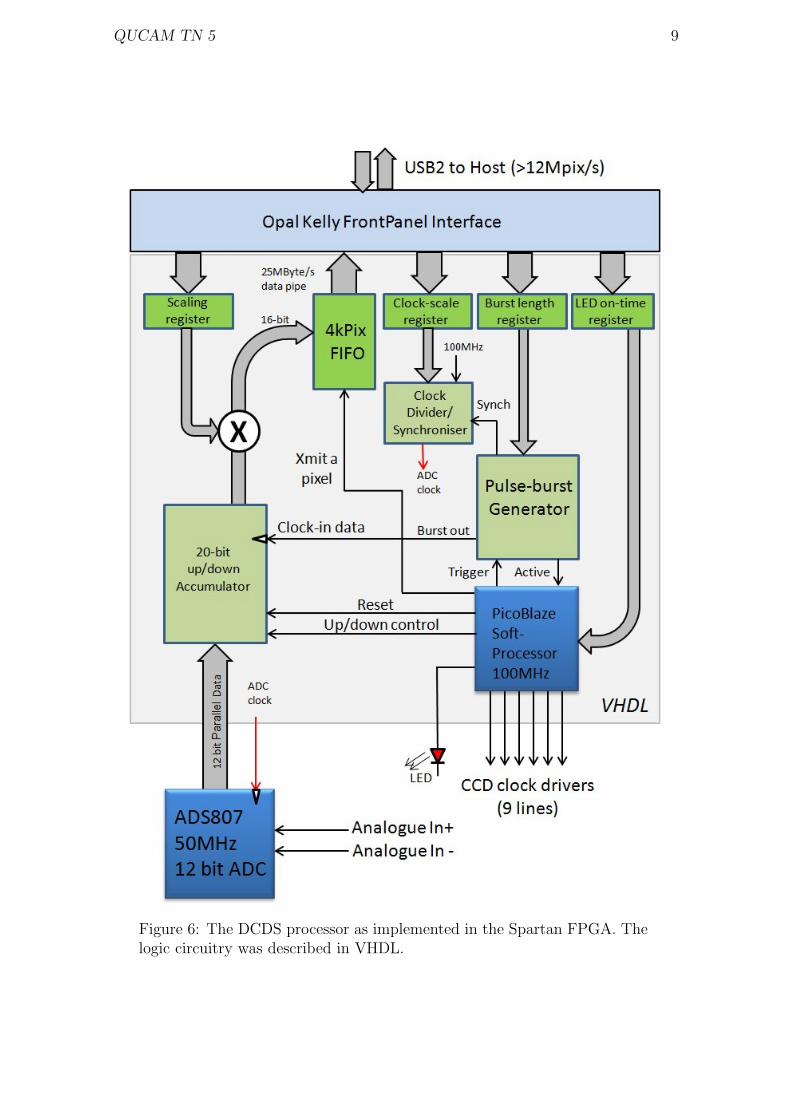
2.6 VHDL-defined circuitry
The DCDS processor was defined in VHDL using the Xilinx ISE development en-vironment. The main elements are shown in Figure 6. The overall sequencing wasdone with a PicoBlaze soft processor running at 100MHz. This was programmed inassembler using the openPICIDE environment. ADC samples were clocked into anup-down Accumulator that performs a differential average of samples obtained inthe reset and signal pedestal regions of the pixel waveform.
QUCAM TN 5 9
Figure 6: The DCDS processor as implemented in the Spartan FPGA. Thelogic circuitry was described in VHDL.
10 QUCAM TN5
The output of the Accumulator is then scaled to 16 bits, the result transmitted to aFIFO and from there to the host PC over the USB interface. The ADC is directlyinterfaced to the FPGA using a parallel port, it is continuously converting but itsdata is only clocked into the accumulator under control of a pulse-burst generator.This generator is implemented as a Finite State Machine and allows multiple samplesto be made of the reset and signal pedestals.
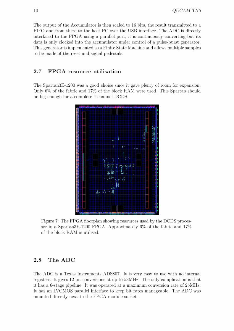
2.7 FPGA resource utilisation
The Spartan3E-1200 was a good choice since it gave plenty of room for expansion.Only 6% of the fabric and 17% of the block RAM were used. This Spartan shouldbe big enough for a complete 4-channel DCDS.
Figure 7: The FPGA floorplan showing resources used by the DCDS proces-sor in a Spartan3E-1200 FPGA. Approximately 6% of the fabric and 17%of the block RAM is utilised.
2.8 The ADC
The ADC is a Texas Instruments ADS807. It is very easy to use with no internalregisters. It gives 12-bit conversions at up to 53MHz. The only complication is thatit has a 6-stage pipeline. It was operated at a maximum conversion rate of 25MHz.It has an LVCMOS parallel interface to keep bit rates manageable. The ADC wasmounted directly next to the FPGA module sockets.
QUCAM TN 5 11
3 Video amplifier characterisation
The video amplifier was characterised using a Rigol signal generator to inject a sinewave signal directly at the input (with the CCD un-socketed).
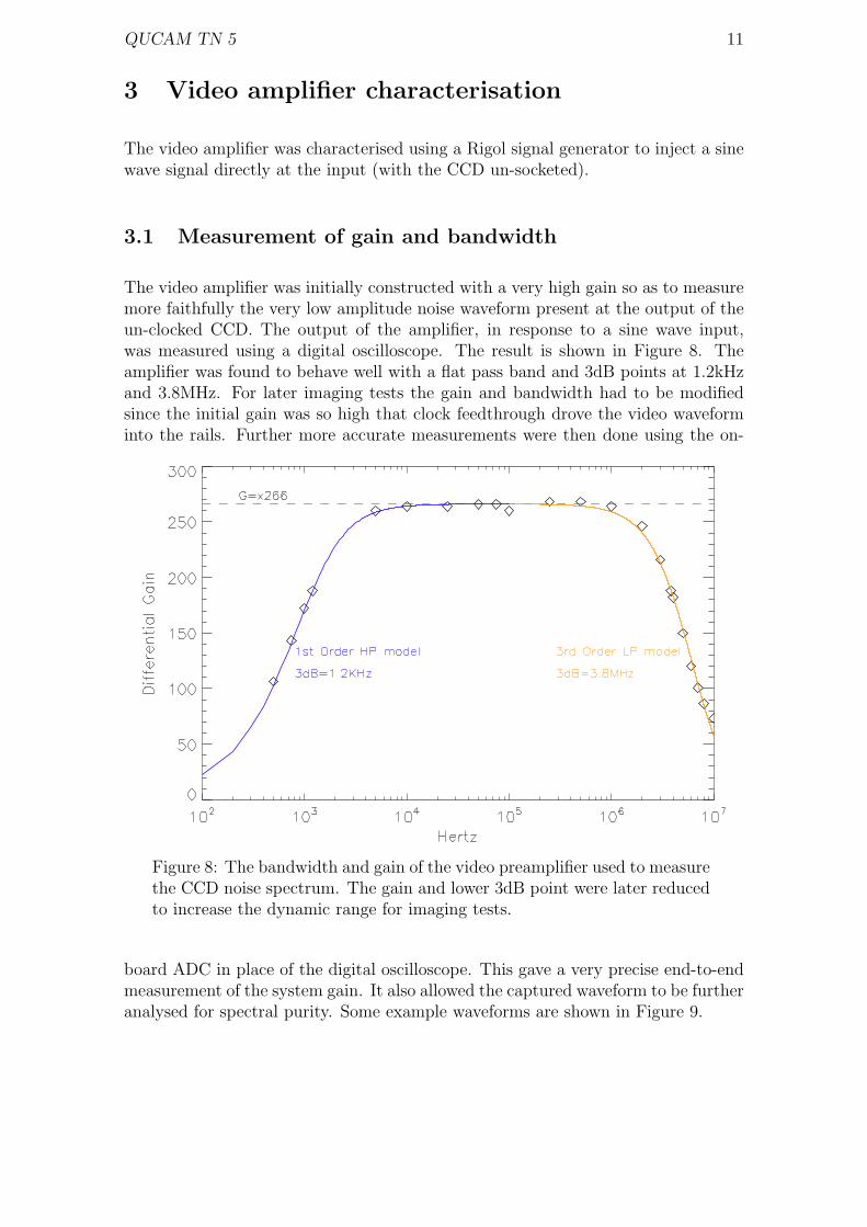
3.1 Measurement of gain and bandwidth
The video amplifier was initially constructed with a very high gain so as to measuremore faithfully the very low amplitude noise waveform present at the output of theun-clocked CCD. The output of the amplifier, in response to a sine wave input,was measured using a digital oscilloscope. The result is shown in Figure 8. Theamplifier was found to behave well with a flat pass band and 3dB points at 1.2kHzand 3.8MHz. For later imaging tests the gain and bandwidth had to be modifiedsince the initial gain was so high that clock feedthrough drove the video waveforminto the rails. Further more accurate measurements were then done using the on-
Figure 8: The bandwidth and gain of the video preamplifier used to measurethe CCD noise spectrum. The gain and lower 3dB point were later reducedto increase the dynamic range for imaging tests.
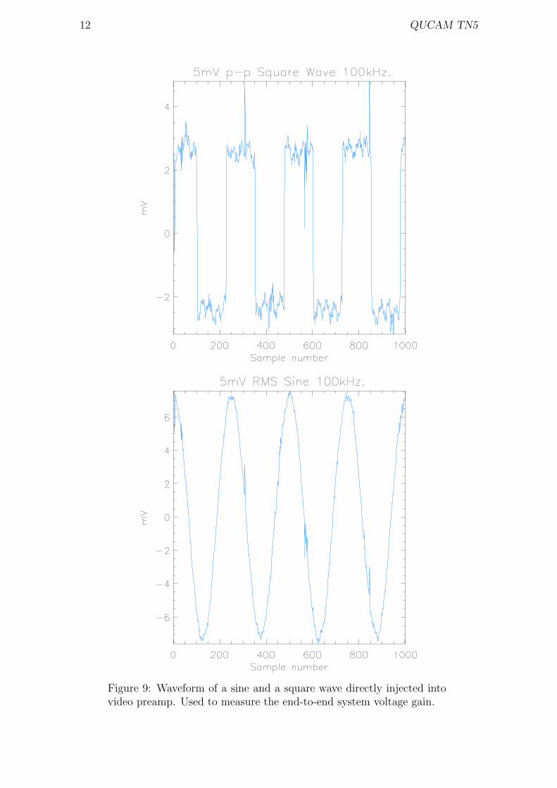
board ADC in place of the digital oscilloscope. This gave a very precise end-to-endmeasurement of the system gain. It also allowed the captured waveform to be furtheranalysed for spectral purity. Some example waveforms are shown in Figure 9.
12 QUCAM TN5
Figure 9: Waveform of a sine and a square wave directly injected intovideo preamp. Used to measure the end-to-end system voltage gain.
QUCAM TN 5 13
3.2 Amplifier noise floor
It was already known from E2V data that the white-noise component of the CCD231was approximately 15nV Hz−0.5. The video preamplifier was designed with the in-tention of keeping its amplitude spectral noise density below 5nV Hz−0.5 so as notto contribute significantly to the total noise.
4 Initial imaging tests
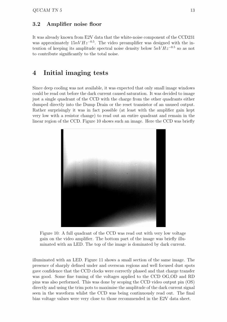
Since deep cooling was not available, it was expected that only small image windowscould be read out before the dark current caused saturation. It was decided to imagejust a single quadrant of the CCD with the charge from the other quadrants eitherdumped directly into the Dump Drain or the reset transistor of an unused output.Rather surprisingly it was in fact possible (at least with the amplifier gain keptvery low with a resistor change) to read out an entire quadrant and remain in thelinear region of the CCD. Figure 10 shows such an image. Here the CCD was briefly
Figure 10: A full quadrant of the CCD was read out with very low voltagegain on the video amplifier. The bottom part of the image was briefly illu-minated with an LED. The top of the image is dominated by dark current.
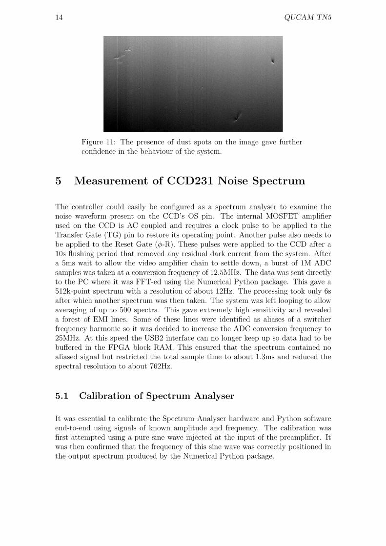
illuminated with an LED. Figure 11 shows a small section of the same image. Thepresence of sharply defined under and overscan regions and well focused dust spotsgave confidence that the CCD clocks were correctly phased and that charge transferwas good. Some fine tuning of the voltages applied to the CCD OG,OD and RDpins was also performed. This was done by scoping the CCD video output pin (OS)directly and using the trim pots to maximise the amplitude of the dark current signalseen in the waveform whilst the CCD was being continuously read out. The finalbias voltage values were very close to those recommended in the E2V data sheet.
14 QUCAM TN5
Figure 11: The presence of dust spots on the image gave furtherconfidence in the behaviour of the system.
5 Measurement of CCD231 Noise Spectrum
The controller could easily be configured as a spectrum analyser to examine thenoise waveform present on the CCD’s OS pin. The internal MOSFET amplifierused on the CCD is AC coupled and requires a clock pulse to be applied to theTransfer Gate (TG) pin to restore its operating point. Another pulse also needs tobe applied to the Reset Gate (ϕ-R). These pulses were applied to the CCD after a10s flushing period that removed any residual dark current from the system. Aftera 5ms wait to allow the video amplifier chain to settle down, a burst of 1M ADCsamples was taken at a conversion frequency of 12.5MHz. The data was sent directlyto the PC where it was FFT-ed using the Numerical Python package. This gave a512k-point spectrum with a resolution of about 12Hz. The processing took only 6safter which another spectrum was then taken. The system was left looping to allowaveraging of up to 500 spectra. This gave extremely high sensitivity and revealeda forest of EMI lines. Some of these lines were identified as aliases of a switcherfrequency harmonic so it was decided to increase the ADC conversion frequency to25MHz. At this speed the USB2 interface can no longer keep up so data had to bebuffered in the FPGA block RAM. This ensured that the spectrum contained noaliased signal but restricted the total sample time to about 1.3ms and reduced thespectral resolution to about 762Hz.
5.1 Calibration of Spectrum Analyser
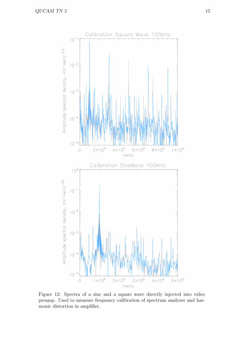
It was essential to calibrate the Spectrum Analyser hardware and Python softwareend-to-end using signals of known amplitude and frequency. The calibration wasfirst attempted using a pure sine wave injected at the input of the preamplifier. Itwas then confirmed that the frequency of this sine wave was correctly positioned inthe output spectrum produced by the Numerical Python package.
QUCAM TN 5 15
Figure 12: Spectra of a sine and a square wave directly injected into videopreamp. Used to measure frequency calibration of spectrum analyser and har-monic distortion in amplifier.
16 QUCAM TN5
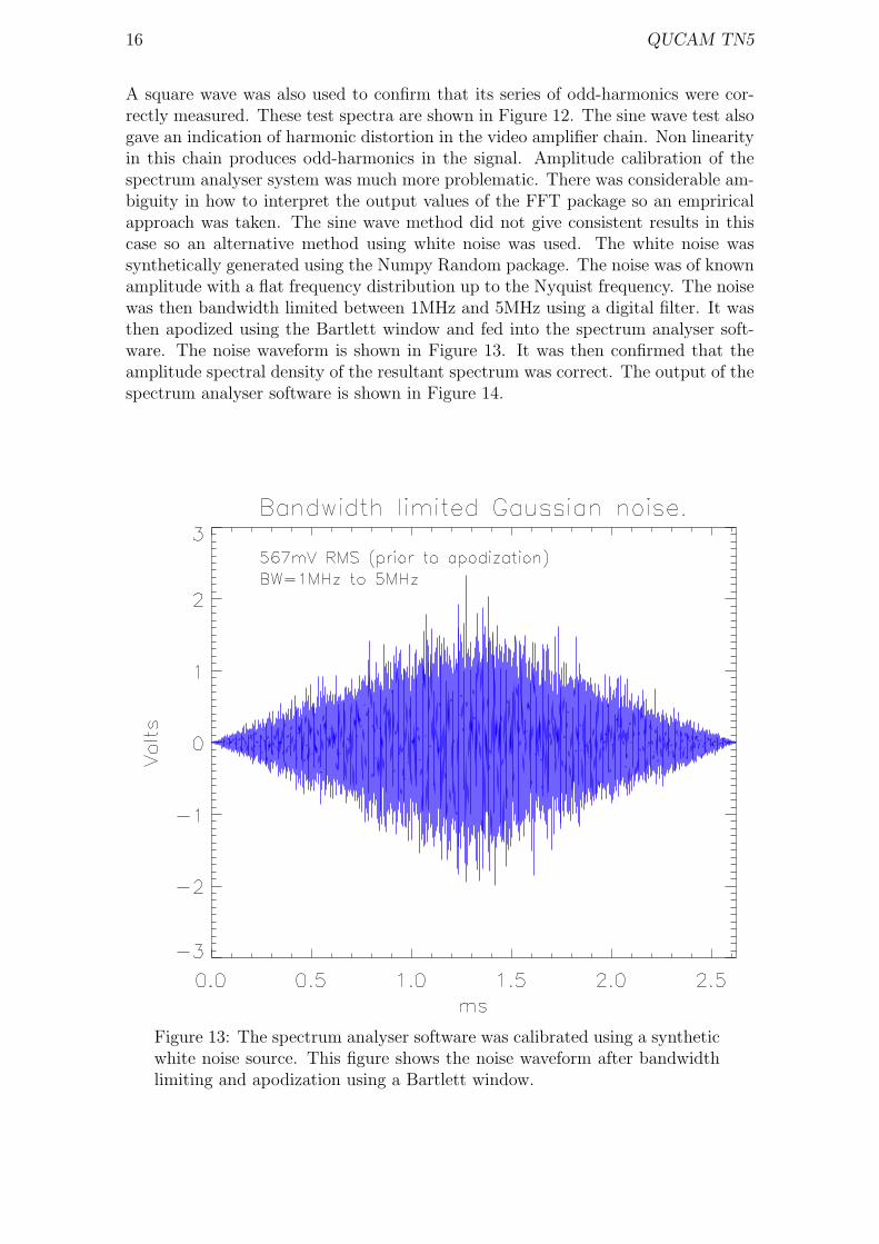
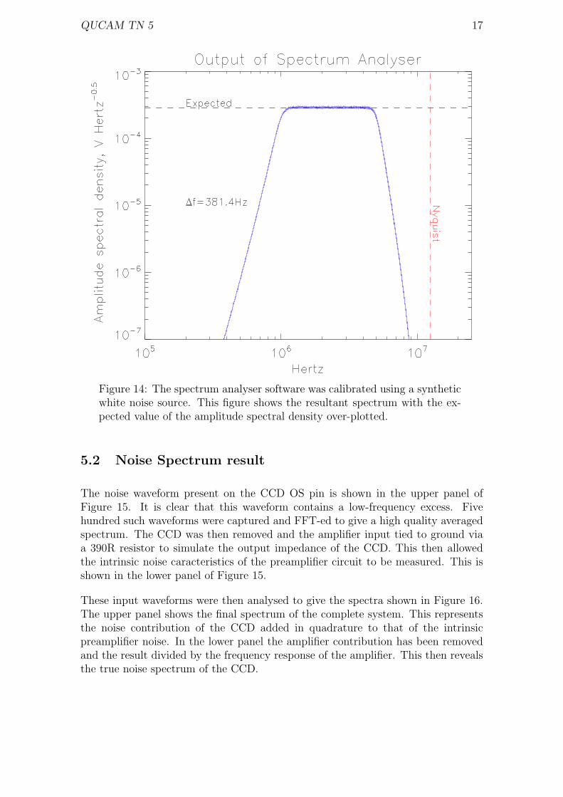
A square wave was also used to confirm that its series of odd-harmonics were cor-rectly measured. These test spectra are shown in Figure 12. The sine wave test alsogave an indication of harmonic distortion in the video amplifier chain. Non linearityin this chain produces odd-harmonics in the signal. Amplitude calibration of thespectrum analyser system was much more problematic. There was considerable am-biguity in how to interpret the output values of the FFT package so an empriricalapproach was taken. The sine wave method did not give consistent results in thiscase so an alternative method using white noise was used. The white noise wassynthetically generated using the Numpy Random package. The noise was of knownamplitude with a flat frequency distribution up to the Nyquist frequency. The noisewas then bandwidth limited between 1MHz and 5MHz using a digital filter. It wasthen apodized using the Bartlett window and fed into the spectrum analyser soft-ware. The noise waveform is shown in Figure 13. It was then confirmed that theamplitude spectral density of the resultant spectrum was correct. The output of thespectrum analyser software is shown in Figure 14.
Figure 13: The spectrum analyser software was calibrated using a syntheticwhite noise source. This figure shows the noise waveform after bandwidthlimiting and apodization using a Bartlett window.
QUCAM TN 5 17
Figure 14: The spectrum analyser software was calibrated using a syntheticwhite noise source. This figure shows the resultant spectrum with the ex-pected value of the amplitude spectral density over-plotted.
5.2 Noise Spectrum result
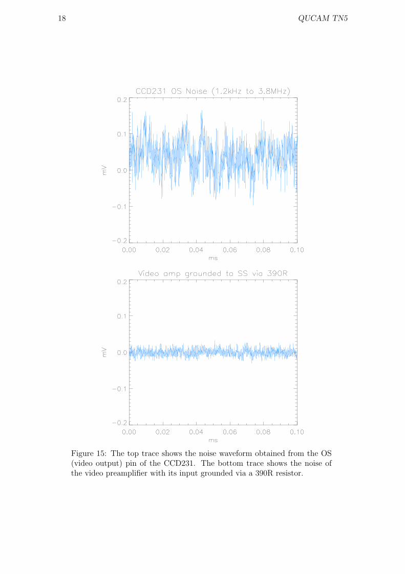
The noise waveform present on the CCD OS pin is shown in the upper panel ofFigure 15. It is clear that this waveform contains a low-frequency excess. Fivehundred such waveforms were captured and FFT-ed to give a high quality averagedspectrum. The CCD was then removed and the amplifier input tied to ground viaa 390R resistor to simulate the output impedance of the CCD. This then allowedthe intrinsic noise caracteristics of the preamplifier circuit to be measured. This isshown in the lower panel of Figure 15.
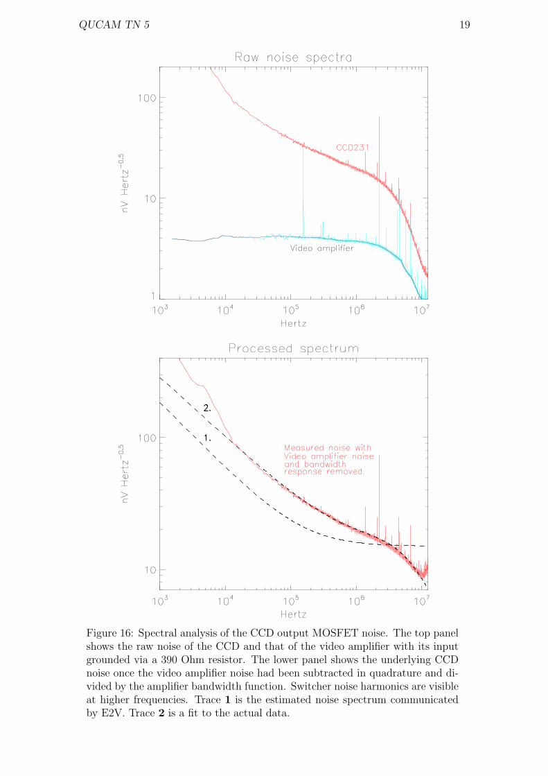
These input waveforms were then analysed to give the spectra shown in Figure 16.The upper panel shows the final spectrum of the complete system. This representsthe noise contribution of the CCD added in quadrature to that of the intrinsicpreamplifier noise. In the lower panel the amplifier contribution has been removedand the result divided by the frequency response of the amplifier. This then revealsthe true noise spectrum of the CCD.
18 QUCAM TN5
Figure 15: The top trace shows the noise waveform obtained from the OS(video output) pin of the CCD231. The bottom trace shows the noise ofthe video preamplifier with its input grounded via a 390R resistor.
QUCAM TN 5 19
Figure 16: Spectral analysis of the CCD output MOSFET noise. The top panelshows the raw noise of the CCD and that of the video amplifier with its inputgrounded via a 390 Ohm resistor. The lower panel shows the underlying CCDnoise once the video amplifier noise had been subtracted in quadrature and di-vided by the amplifier bandwidth function. Switcher noise harmonics are visibleat higher frequencies. Trace 1 is the estimated noise spectrum communicatedby E2V. Trace 2 is a fit to the actual data.
20 QUCAM TN5
5.3 Comparison with the E2V noise model
The noise in a CCD output MOSFET amplifier is described by Equation 1. Thereare two terms, a white noise component with flat spectral density and a so-calledflicker noise component with a power spectral density proportional to the inverse ofthe frequency. fC is the corner frequency where the flicker noise has a density equalto the white noise. E2V estimate the CCD231 to have NG equal to 15nV Hz−0.5 andfC to be 150kHz.
N(f)1 = NG.
(1 +
fCf
)0.5
V Hz−0.5. (1)
As can be seen the actual noise spectrum was rather different. It is best described byEquation 2. The drop-off at higher frequencies is described by a single-pole low-passfilter with a 3dB point at 6MHz. This compares with the CCD amplifier bandwidthof 8MHz quoted by E2V.
N(f)2 = 15nV.
(1 +
600kHz
f
)0.45
V Hz−0.5. (2)
Both the E2V-estimated spectrum and the measured spectrum are shown overplot-ted in the bottom panel of Figure 16. In conclusion, the corner frequency of theCCD under test was found to be 600kHz as opposed to the 150kHz quoted by E2V.The actual CCD used was an engineering grade sample (S/N 08493-02-01, TypeCCD231-85-5-D84) and since this came without a data sheet its factory measurednoise characteristics are unknown.
6 Video waveform processing technique
As can be seen in Figure 1 the reset and signal pedestal regions are relatively cleansince there are no clock transitions during these time periods. In order that thevoltage step at charge dump can be measured as precisely as possible, the pedestalsneed to be measured for as long a time as possible. This leads to a trade-off betweenread time and read noise.
6.1 The differential averager
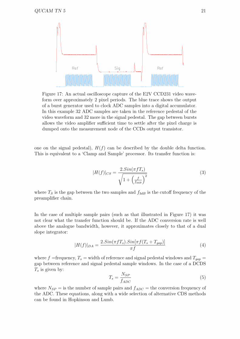
The DCDS system functions as a differential averager. It takes multiple samples ofthe reset pedestal and calculates an average value. It later takes the same numberof samples of the signal pedestal, performs a second average and then subtracts oneresult from the other. Figure 17. shows the CCD video waveform with the ADCstart-convert pulse phasing overlaid.
6.2 The video processor transfer function
The differential averager can be thought of as a digital filter with transfer functionH(f). In the limit of a single ADC conversion pair (one on the reset pedestal and
QUCAM TN 5 21
Figure 17: An actual oscilloscope capture of the E2V CCD231 video wave-form over approximately 2 pixel periods. The blue trace shows the outputof a burst generator used to clock ADC samples into a digital accumulator.In this example 32 ADC samples are taken in the reference pedestal of thevideo waveform and 32 more in the signal pedestal. The gap between burstsallows the video amplifier sufficient time to settle after the pixel charge isdumped onto the measurement node of the CCDs output transistor.
one on the signal pedestal), H(f) can be described by the double delta function.This is equivalent to a ‘Clamp and Sample’ processor. Its transfer function is:
|H(f)|CS =2.Sin(πfTs)√1 +
(f
f3dB
)2(3)
where TS is the gap between the two samples and f3dB is the cutoff frequency of thepreamplifier chain.
In the case of multiple sample pairs (such as that illustrated in Figure 17) it wasnot clear what the transfer function should be. If the ADC conversion rate is wellabove the analogue bandwidth, however, it approximates closely to that of a dualslope integrator:
|H(f)|DA =2.Sin(πfTs).Sin[πf(Ts + Tgap)]
πf(4)
where f =frequency, Ts = width of reference and signal pedestal windows and Tgap =gap between reference and signal pedestal sample windows. In the case of a DCDSTs is given by:
Ts =NSP
fADC
(5)
where NSP = is the number of sample pairs and fADC = the conversion frequency ofthe ADC. These equations, along with a wide selection of alternative CDS methodscan be found in Hopkinson and Lumb.

22 QUCAM TN5
6.3 Relationship between transfer function and CCD readnoise
The CDS transfer function acts as a digital filter on the noise spectrum of the CCD,acting to maximise the signal whilst at the same time minimising the noise. Thisfiltering process is by no means optimum (as explored by Clapp) but it is certainlyclose.
Figure 18: Filtering effect of a differential averager on the noise spectrumof the CCD231.
QUCAM TN 5 23
Figure 18 shows the transfer function H(f) of a differential averager with NSP = 50,fADC = 25MHz and Tgap = 0.6us. The lower panel of this figure shows the noisespectrum of the CCD before and after filtering by H(f). It is then possible tointegrate the filtered noise spectrum across the full passband to yield an RMS voltagenoise at the output of the CCD. The integration required is given by Equation 6.
Noise =
[∫ fmax
0
[H(f).N(f)]2 df
]0.5V oltsRMS, (6)
where fmax =full bandwidth (in this case about 2.5MHz), N(f) = amplitude spectraldensity of CCD, H(f) = transfer function of differential averager. This then allowsus to predict in theory the read noise we can expect from any hypothetical differentialaverager. The actual read noise obtained can then be compared against theory toestablish the efficiency of the implementation.
6.4 Implementation of a Digital CDS
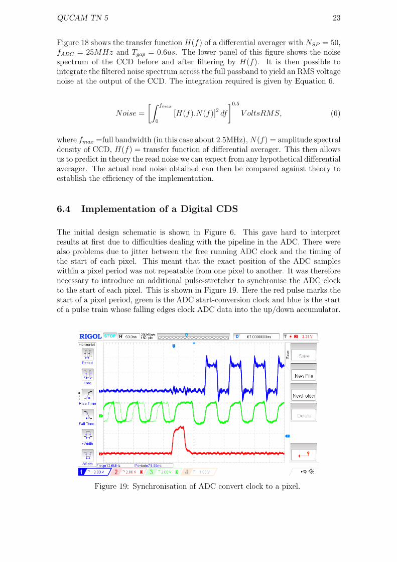
The initial design schematic is shown in Figure 6. This gave hard to interpretresults at first due to difficulties dealing with the pipeline in the ADC. There werealso problems due to jitter between the free running ADC clock and the timing ofthe start of each pixel. This meant that the exact position of the ADC sampleswithin a pixel period was not repeatable from one pixel to another. It was thereforenecessary to introduce an additional pulse-stretcher to synchronise the ADC clockto the start of each pixel. This is shown in Figure 19. Here the red pulse marks thestart of a pixel period, green is the ADC start-conversion clock and blue is the startof a pulse train whose falling edges clock ADC data into the up/down accumulator.
Figure 19: Synchronisation of ADC convert clock to a pixel.
24 QUCAM TN5
This oscilloscope trace is triggered on the pixel-start pulse (red). Notice that thereis jitter visible on the ADC clock but that it becomes synchronised to the pixel afterthe pixel-start pulse goes low. This ensures that ADC samples are taken at thesame relative positions within all pixels of the image. If this is not done then noiseartefacts appear in the bias frames.
7 In-depth imaging characterisation
It was essential to collect high quality images from the CCD in order to establish thesystem gain using the photon-transfer method (see Janesick). For the purposes ofphoton transfer analysis dark current frames serve equally as well as light-exposedimages; both are subject to Poissonian statistics. Being able to measure the gain isessential since it allows us to express noise performance in units of e− RMS.
7.1 Photon transfer gain measurement.
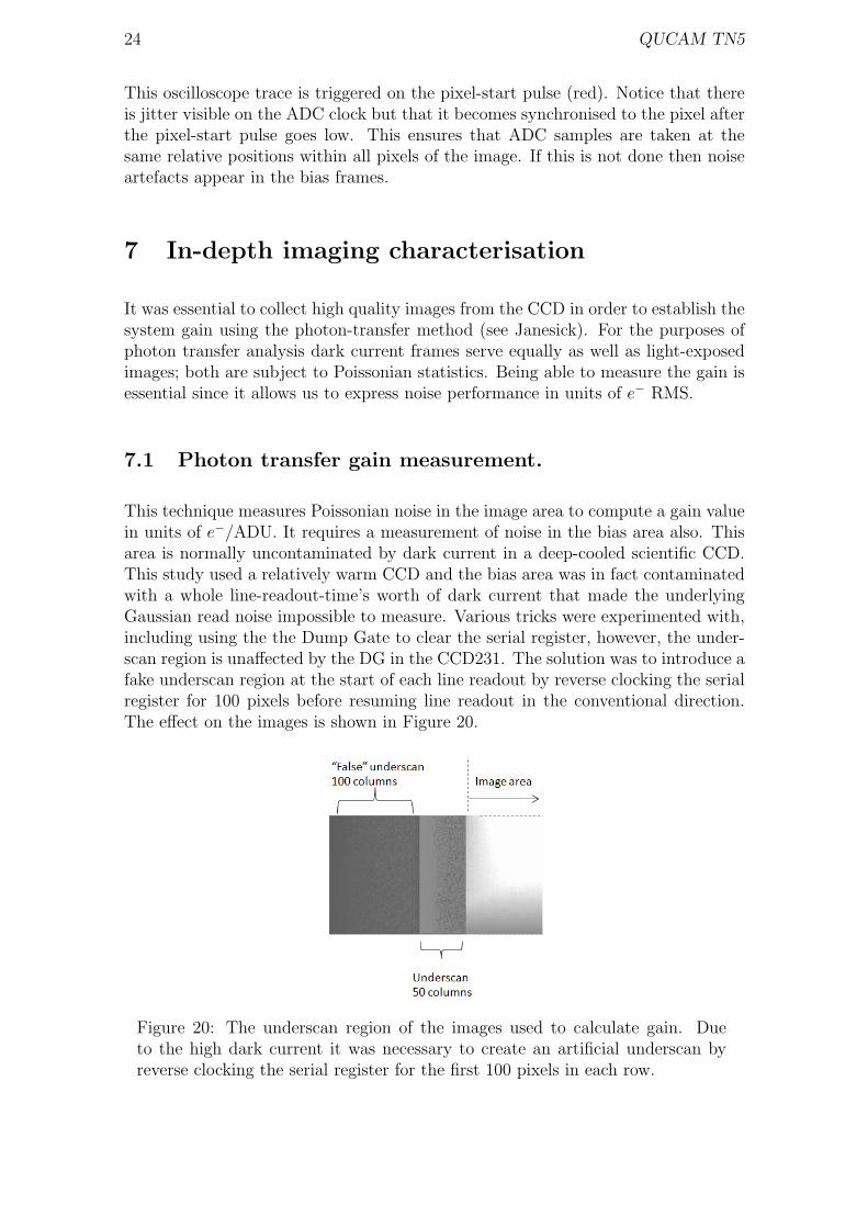
This technique measures Poissonian noise in the image area to compute a gain valuein units of e−/ADU. It requires a measurement of noise in the bias area also. Thisarea is normally uncontaminated by dark current in a deep-cooled scientific CCD.This study used a relatively warm CCD and the bias area was in fact contaminatedwith a whole line-readout-time’s worth of dark current that made the underlyingGaussian read noise impossible to measure. Various tricks were experimented with,including using the the Dump Gate to clear the serial register, however, the under-scan region is unaffected by the DG in the CCD231. The solution was to introduce afake underscan region at the start of each line readout by reverse clocking the serialregister for 100 pixels before resuming line readout in the conventional direction.The effect on the images is shown in Figure 20.
Figure 20: The underscan region of the images used to calculate gain. Dueto the high dark current it was necessary to create an artificial underscan byreverse clocking the serial register for the first 100 pixels in each row.
QUCAM TN 5 25
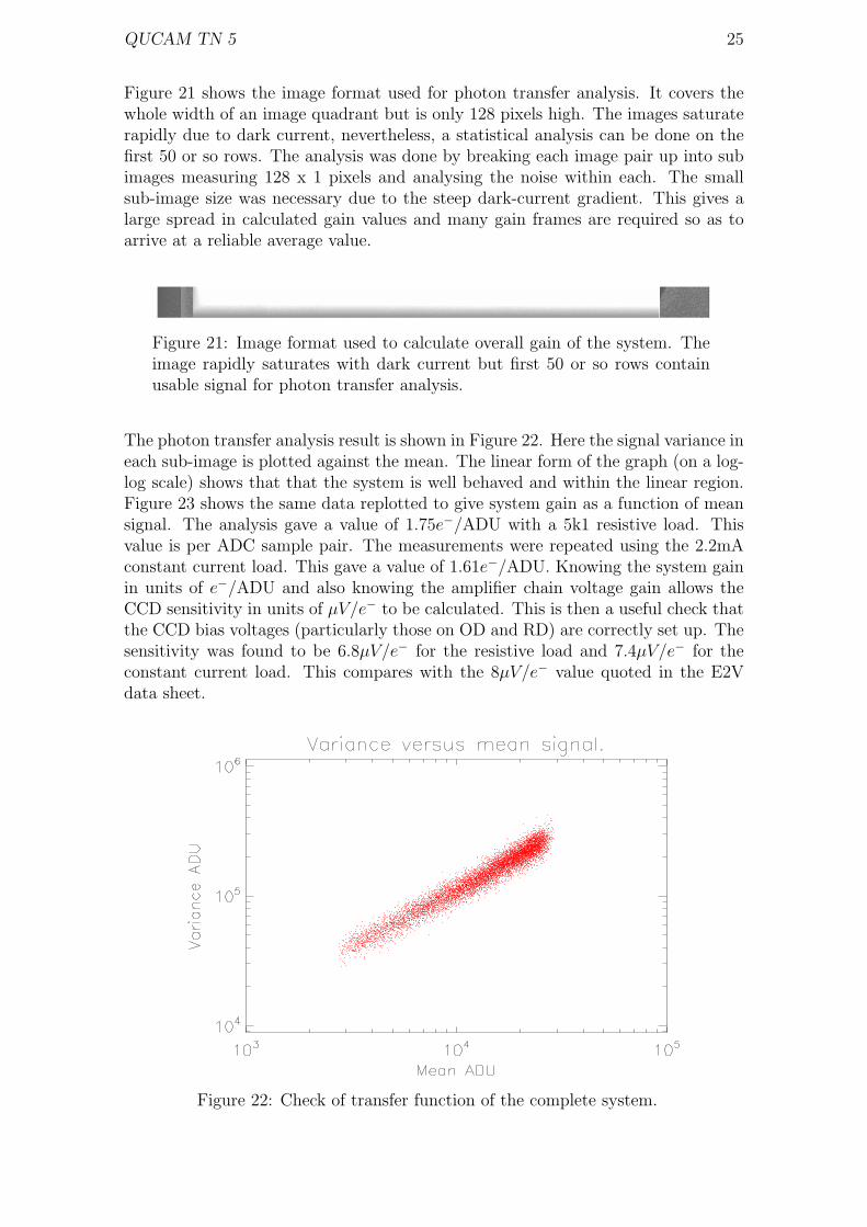
Figure 21 shows the image format used for photon transfer analysis. It covers thewhole width of an image quadrant but is only 128 pixels high. The images saturaterapidly due to dark current, nevertheless, a statistical analysis can be done on thefirst 50 or so rows. The analysis was done by breaking each image pair up into subimages measuring 128 x 1 pixels and analysing the noise within each. The smallsub-image size was necessary due to the steep dark-current gradient. This gives alarge spread in calculated gain values and many gain frames are required so as toarrive at a reliable average value.
Figure 21: Image format used to calculate overall gain of the system. Theimage rapidly saturates with dark current but first 50 or so rows containusable signal for photon transfer analysis.
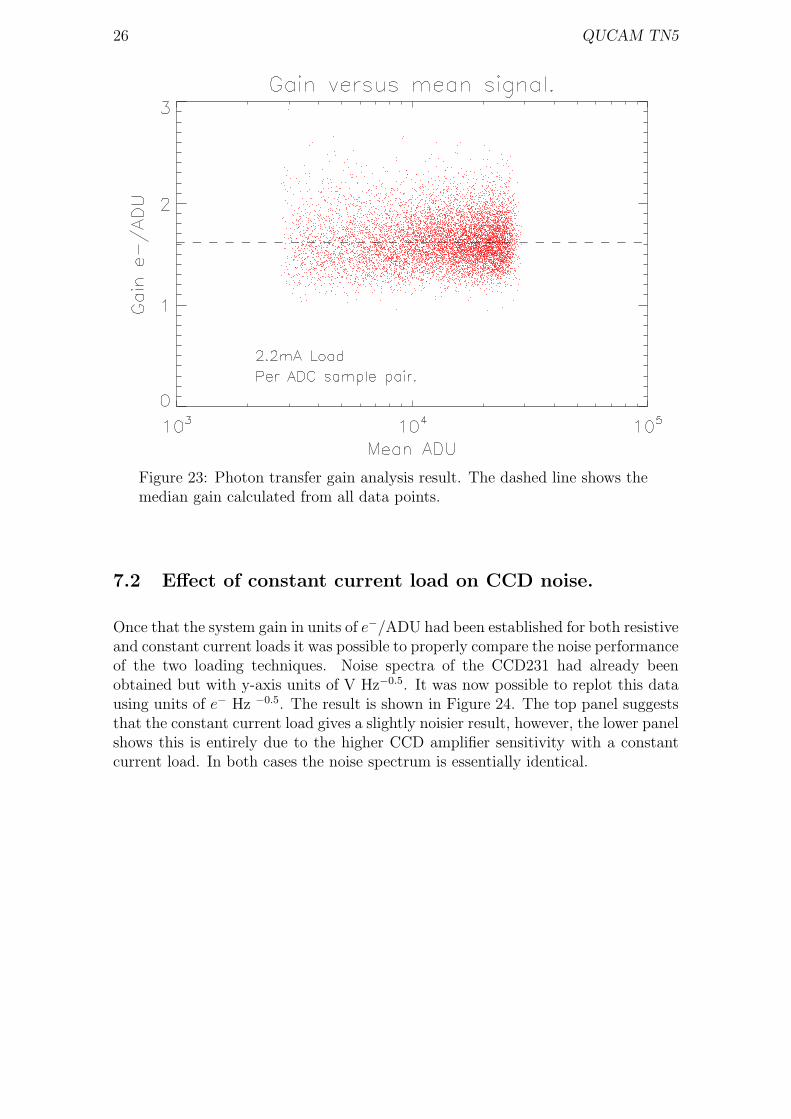
The photon transfer analysis result is shown in Figure 22. Here the signal variance ineach sub-image is plotted against the mean. The linear form of the graph (on a log-log scale) shows that that the system is well behaved and within the linear region.Figure 23 shows the same data replotted to give system gain as a function of meansignal. The analysis gave a value of 1.75e−/ADU with a 5k1 resistive load. Thisvalue is per ADC sample pair. The measurements were repeated using the 2.2mAconstant current load. This gave a value of 1.61e−/ADU. Knowing the system gainin units of e−/ADU and also knowing the amplifier chain voltage gain allows theCCD sensitivity in units of µV/e− to be calculated. This is then a useful check thatthe CCD bias voltages (particularly those on OD and RD) are correctly set up. Thesensitivity was found to be 6.8µV/e− for the resistive load and 7.4µV/e− for theconstant current load. This compares with the 8µV/e− value quoted in the E2Vdata sheet.
Figure 22: Check of transfer function of the complete system.
26 QUCAM TN5
Figure 23: Photon transfer gain analysis result. The dashed line shows themedian gain calculated from all data points.
7.2 Effect of constant current load on CCD noise.
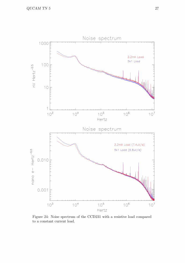
Once that the system gain in units of e−/ADU had been established for both resistiveand constant current loads it was possible to properly compare the noise performanceof the two loading techniques. Noise spectra of the CCD231 had already beenobtained but with y-axis units of V Hz−0.5. It was now possible to replot this datausing units of e− Hz −0.5. The result is shown in Figure 24. The top panel suggeststhat the constant current load gives a slightly noisier result, however, the lower panelshows this is entirely due to the higher CCD amplifier sensitivity with a constantcurrent load. In both cases the noise spectrum is essentially identical.
QUCAM TN 5 27
Figure 24: Noise spectrum of the CCD231 with a resistive load comparedto a constant current load.
28 QUCAM TN5
8 DCDS noise results
With the controller now fully characterised it was possible to evaluate the noiseperformance of the DCDS as a function of both number of sample pairs and thefrequency of the ADC. The results could then be compared to the theoretical pre-dictions.
8.1 Effect of ADC frequency
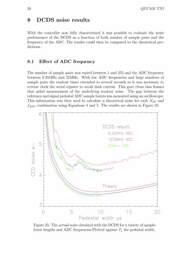
The number of sample pairs was varied between 1 and 255 and the ADC frequencybetween 6.25MHz and 25MHz. With low ADC frequencies and large numbers ofsample pairs the readout times extended to several seconds so it was necessary toreverse clock the serial register to avoid dark current. This gave clean bias framesthat aided measurement of the underlying readout noise. The gap between thereference and signal pedestal ADC sample bursts was measured using an oscilloscope.This information was then used to calculate a theoretical noise for each NSP andfADC combination using Equations 4 and 5. The results are shown in Figure 25.
Figure 25: The actual noise obtained with the DCDS for a variety of sample-burst lengths and ADC frequencies.Plotted against Ts the pedestal width.
QUCAM TN 5 29
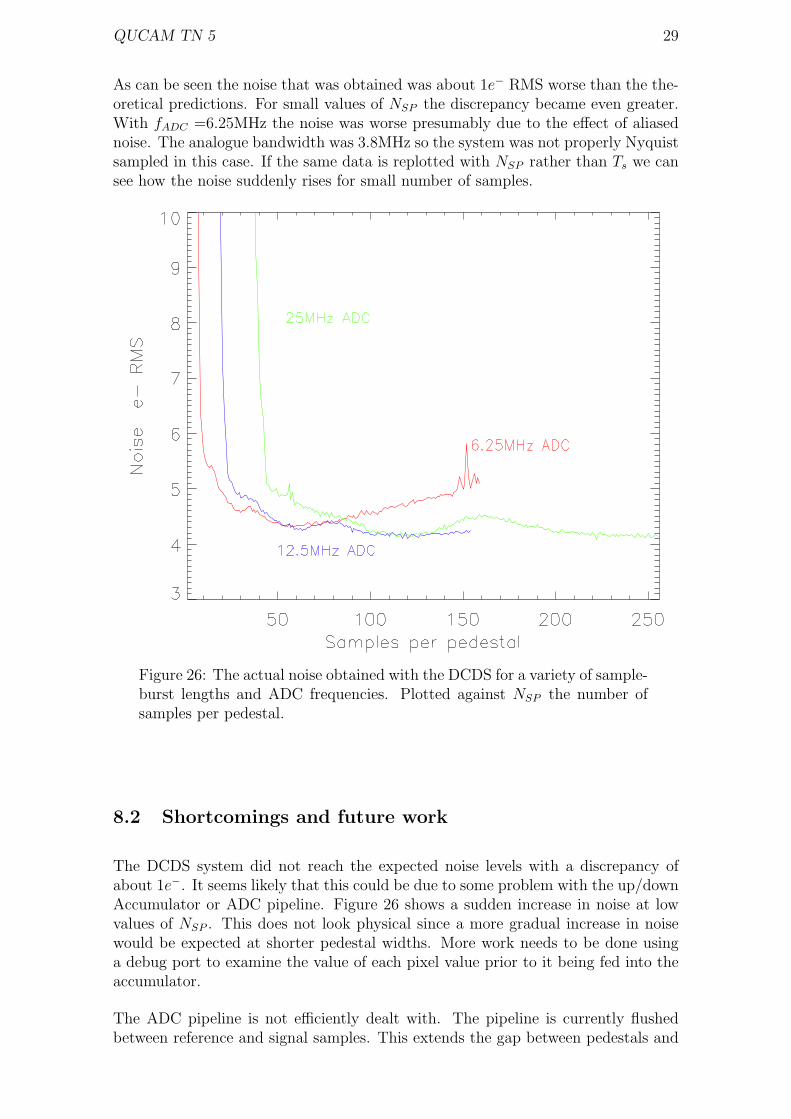
As can be seen the noise that was obtained was about 1e− RMS worse than the the-oretical predictions. For small values of NSP the discrepancy became even greater.With fADC =6.25MHz the noise was worse presumably due to the effect of aliasednoise. The analogue bandwidth was 3.8MHz so the system was not properly Nyquistsampled in this case. If the same data is replotted with NSP rather than Ts we cansee how the noise suddenly rises for small number of samples.
Figure 26: The actual noise obtained with the DCDS for a variety of sample-burst lengths and ADC frequencies. Plotted against NSP the number ofsamples per pedestal.
8.2 Shortcomings and future work
The DCDS system did not reach the expected noise levels with a discrepancy ofabout 1e−. It seems likely that this could be due to some problem with the up/downAccumulator or ADC pipeline. Figure 26 shows a sudden increase in noise at lowvalues of NSP . This does not look physical since a more gradual increase in noisewould be expected at shorter pedestal widths. More work needs to be done usinga debug port to examine the value of each pixel value prior to it being fed into theaccumulator.
The ADC pipeline is not efficiently dealt with. The pipeline is currently flushedbetween reference and signal samples. This extends the gap between pedestals and
30 QUCAM TN5
impacts the noise. It would be better to do the flush at the end of an image linerather than within each pixel.
Another obvious experiment would be to use non-constant ADC weightings. Thishas the potential to reduce the read noise further by optimal filtering (see Clapp).
The corner frequency was much higher than that quoted by E2V. The reasons forthis need to be further investigated.
References
Hopkinson and Lumb, Noise Reduction techniques for CCD image sensors, J.Phys. E:Sci Instrum., Vol 15. 1982.
Clapp, Development of a test system for the characterisation of DCDS CCD readout tech-niques, SPIE 2012, Vol 8453.
Janesick, Scientific Charge-Coupled Devices, SPIE Press 2001.