technical university tallinn, estonia component level dy defect mapping hierarchical test generation...
TRANSCRIPT

Technical University Tallinn, ESTONIA
Component level
dy
Defect mapping
Hierarchical Test Generation
x1
x2
x3
x4
x5
System level
Wd
Logic levelError
Defect
Hierarchical test (fault propagation)
y*
&
&
&
1
&
&
&
R2M3
+M1
*M2
R1
IN
Logic level
Transistor level
RT Level

Research in ATI© Raimund Ubar
x1
x2
y
x3
x4 x5
x6 x7
0
11
0
x 1
x2
y
x 3
x4 x5
x6 x7
0
1
1
0
0
2
1
Error
1 0 x1 x2
x3 = 1 x4 x5 x6 x7
y
0
0 0 F (X)
SSBDD
mlm
lm ,1
m1
m0mT, 1
mT, 0
lm ,0
Root node
Binary Decision Diagrams

Research in ATI© Raimund Ubar
Generalization of BDDs
m
y1
0
lm
l1
l0
Gy
m
Y 1
0
2
h
FkFn
l0l1
l2lh
lklk+1
Fk+1
ln
lmGY
Binary DD 2 terminal nodes and 2 edges from each node
General case of DD n 2 terminal nodes and n 2 edges from each node
Novelty: Boolean methods can be generalized in a straightforward way to higher functional levels
3

Technical University Tallinn, ESTONIA
Faults and High-Level Decision Diagrams
RTL-statement:
R2M3
e+M1
a
*M2
b
R1
IN
c
d
y1 y2 y3 y4
y4
y3 y1 R1 + R2
IN + R2
R1* R2
IN* R2
y2
R2 0
1
2 0
1
0
1
0
1
0
R2
IN
R12
3
Terminal nodes
RTL-statement faults: data storage, data transfer, data manipulation faults
Nonterminal nodes
RTL-statement faults: label, timing condition, logical condition, register decoding, operation decoding,control faults
K: (If T,C) RD F(RS1,RS2,…RSm), N
Testing concepton the DD-model(uniform for all nodes): 1) Exhaustive testing2) Optimization
Technical University Tallinn, ESTONIA
Test Generation for Digital Systems
R2M3
e+M1
a
*M2
b
R1
IN
c
d
y1 y2 y3 y4
y4
y3 y1 R1 + R2
IN + R2
R1 * R2
IN* R2
y2
R2 0
1
2 0
1
0
1
0
1
0
R2
IN
R12
3
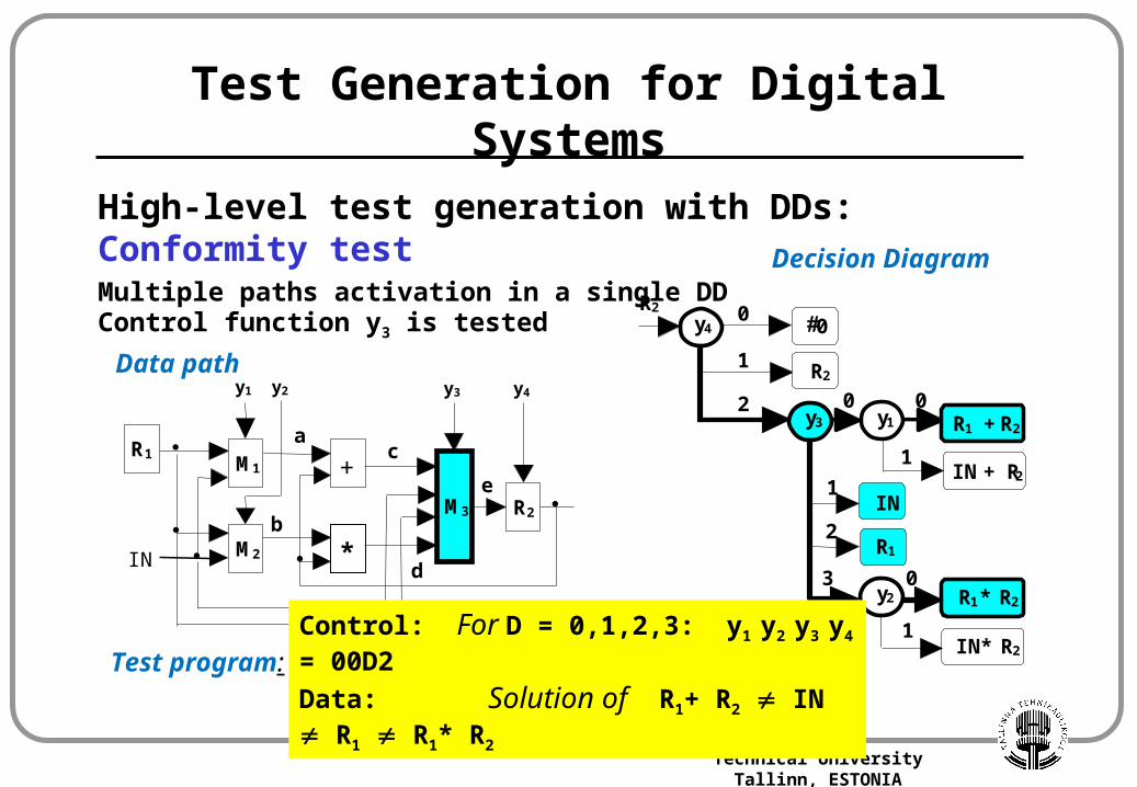
Multiple paths activation in a single DDControl function y3 is tested
Data path
Decision Diagram
High-level test generation with DDs: Conformity test
Control: For D = 0,1,2,3: y1 y2 y3 y4 = 00D2
Data: Solution of R1+ R2 IN R1 R1* R2
Test program:

Technical University Tallinn, ESTONIA
Test Generation for Digital Systems
R2M3
e+M1
a
*M2
b
R1
IN
c
d
y1 y2 y3 y4
High-level test generation with DDs: Conformity test
Test template:Test program:
For D = 0,1,2,3BeginLoad R1 = IN1Load R2 = IN2Apply IN = IN3 y1 y2 y3 y4 = 00D2 Read R2 End
R2(D)
Control: For D = 0,1,2,3: y1 y2 y3 y4 = 00D2
Data: Solution of R1+ R2 IN R1 R1* R2

Technical University Tallinn, ESTONIA
Test Generation for Digital Systems
R2M3
e+M1
a
*M2
b
R1
IN
c
d
y1 y2 y3 y4
y4
y3 y1 R1 + R2
IN + R2
R1 * R2
IN* R2
y2
R2 0
1
2 0
1
0
1
0
1
0
R2
IN
R12
3
Single path activation in a single DDData function R1* R2 is tested
Data path
Decision Diagram
High-level test generation with DDs: Scanning test
Control: y1 y2 y3 y4 = 0032
Data: For all specified pairs of (R1, R2)
Test program:

Technical University Tallinn, ESTONIA
Test Generation for Digital Systems
R2M3
e+M1
a
*M2
b
R1
IN
c
d
y1 y2 y3 y4
High-level test generation with DDs: Scanning test
Control: y1 y2 y3 y4 = 0032
Data: For all specified pairs of (R1, R2)
Test template:Test program:
For j=1,nBeginLoad R1 = IN(j1)Load R2 = IN(j2)y1 y2 y3 y4 = 0032: Read R2 End
IN(j1) IN(j2) R2(j)
Test data Test results

Technical University Tallinn, ESTONIA
Scan-Path for Making Systems Transparent
y4
y3 y1 R1 + R2
IN + R2
R1 * R2
IN* R2
y2
R2 0
1
2 0
1
0
1
0
1
0
R2
IN
R12
3
Hierarhical test generation with Scan-Path:
Bus
Scan-Out
M3
e+M1
a
*M2
b
R1
IN
c
d
y1 y2 y3 y4
Control Part
R2
Scan-In
Data Part

Technical University Tallinn, ESTONIA
Testing with Minimal DFT for Scan-Path
M3
e+M1
a
*M2
b
R1
IN
c
d
y1 y2 y3 y4
y4
y3 y1 R1 + R2
IN + R2
R1 * R2
IN* R2
y2
R2 0
1
2 0
1
0
1
0
1
0
R2
IN
R12
3
Hierarhical test generation with Scan-Path:
Control Part
R2Bus
Scan-In
Scan-Out
Data Part

Technical University Tallinn, ESTONIA
Test Generation for Microprocessors
I1: MVI A,D A IN
I2: MOV R,A R A
I3: MOV M,R OUT R
I4: MOV M,A OUT IA
I5: MOV R,M R IN
I6: MOV A,M A IN
I7: ADD R A A + R
I8: ORA R A A R
I9: ANA R A A R
I10: CMA A,D A A
Test program generation for a microprocessor (example):
Instruction set:
I R3
A
OUT4
I A2
R
IN5
R
1,3,4,6-10
I IN1,6
A
A2,3,4,5
A + R7
A R8
A R9
A10
DD-model of themicroprocessor:

Technical University Tallinn, ESTONIA
Decision Diagrams for Microprocessors
High-Level DD-based structure of the microprocessor (example):
DD-model of themicroprocessor:
OUT
R
A
IN
I
I R3
A
OUT4
I A2
R
IN5
R
1,3,4,6-10
I IN1,6
A
A2,3,4,5
A + R7
A R8
A R9
A10
A + R

Technical University Tallinn, ESTONIA
Test Program Synthesis for Microprocessors
DD-model of themicroprocessor:
Scanning test program for adder:
Instruction sequence T = I5 (R)I1 (A)I7 I4for all needed pairs of (A,R)
OUT I4
A I7
A
R
I1
IN(2)
IN(1)
R I5
Time:t t - 1 t - 2 t - 3
Observation Test Load
I R3
A
OUT4
I A2
R
IN5
R
1,3,4,6-10
I IN1,6
A
A2,3,4,5
A + R7
A R8
A R9
A10

Technical University Tallinn, ESTONIA
Test Program Synthesis for Microprocessors
Scanning test program for adder:
Instruction sequence T = I5 (R)I1 (A)I7 I4for all needed pairs of (A,R)
OUT I4
A I7
A
R
I1
IN(2)
IN(1)
R I5
Time:t t - 1 t - 2 t - 3
Observation Test Load
Test program:
For j=1,nBeginI5: Load R = IN(j1)I1: Load A = IN(j2)I7: ADD A = A + RI4: Read A End
IN(j1) IN(j2) A
Test data Test results

Technical University Tallinn, ESTONIA
Test Program Synthesis for Microprocessors
DD-model of themicroprocessor:
Conformity test program for decoding I:
Instruction sequence T = I5 I1 D I4
for all DI1 - I10 at given A,R,IN(3)
OUT I4
A I = ID
A
R
I1
IN(2)
IN(1)
R I5
Time:t t - 1 t - 2 t - 3
Observation Test Load
I R3
A
OUT4
I A2
R
IN5
R
1,3,4,6-10
A I IN1,6
A2,3,4,5
A + R7
A R8
A R9
A10
IN(3)

Technical University Tallinn, ESTONIA
Test Program Synthesis for Microprocessors
Conformity test program for decoding I:
Instruction sequence T = I5 I1 D I4
for all DI1 - I10 at given A,R,IN(3)
OUT I4
A I = ID
A
R
I1
IN(2)
IN(1)
R I5
Time:t t - 1 t - 2 t - 3
Observation Test Load
IN(3)
Test program:
For j=1,nBeginI5: Load R = IN(1)I1: Load A = IN(2)ID: DI4: Read A End
Ij A
Test data Test results

Technical University Tallinn, ESTONIA
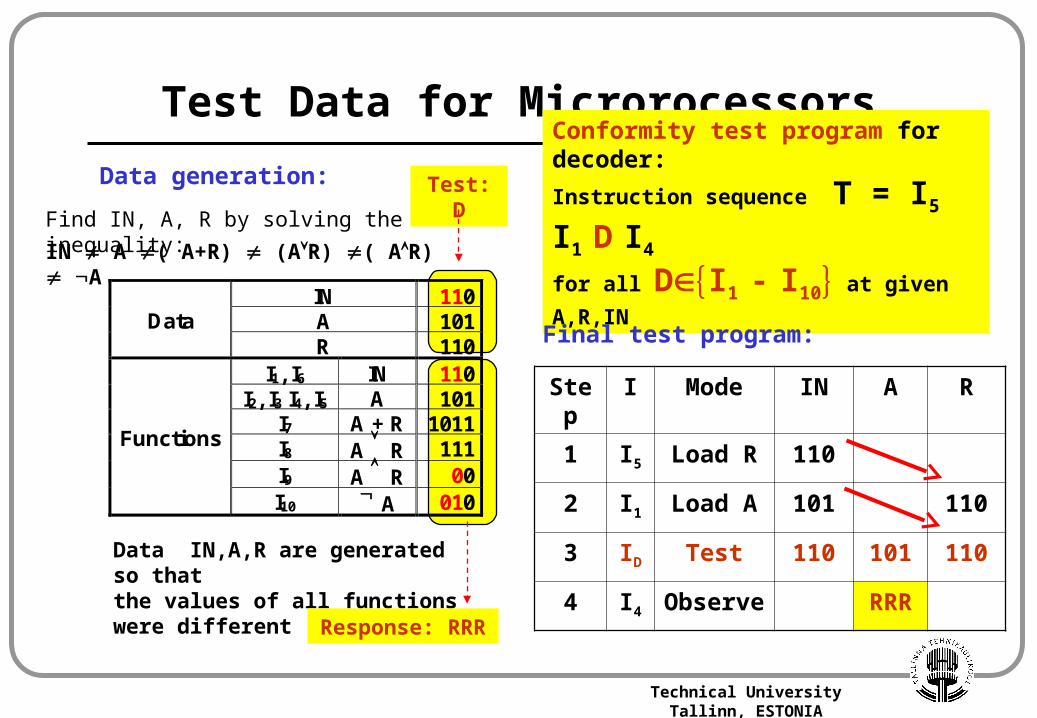
Test Data for Microrocessors
Conformity test program for I in A:
Instruction sequence T = I5 I1 D I4
for all DI1 - I10 at given A,R,IN
IN 110 A 101
Data
R 110 I1, I6 IN 110
I2, I3 I4, I5 A 101 I7 A + R 1011 I8 A R 111 I9 A R 00
Functions
I10 A 010
Data IN,A,R are generated so that the values of all functions were different
Response: RRR
Test: DTest data generation:
IN A ( A+R) (AR) ( AR) A
Find IN, A, R by solving the inequality:
A I IN1,6
A2,3,4,5
A + R7
A R8
A R9
A10
Technical University Tallinn, ESTONIA
Test Data for Microrocessors
Conformity test program for decoder:
Instruction sequence T = I5 I1 D I4
for all DI1 - I10 at given A,R,IN
Data generation:
IN 110 A 101
Data
R 110 I1, I6 IN 110
I2, I3 I4, I5 A 101 I7 A + R 1011 I8 A R 111 I9 A R 00
Functions
I10 A 010
Data IN,A,R are generated so that the values of all functions were different
Final test program:
Step I Mode IN A R
1 I5 Load R 110
2 I1 Load A 101 110
3 ID Test 110 101 110
4 I4 Observe RRR
Response: RRR
Test: D
IN A ( A+R) (AR) ( AR) A
Find IN, A, R by solving the inequality:

Research in ATI© Raimund Ubar
19
OP B Semantic RT level operations
00 READ memory R(A1) = M(A) PC = PC + 21 WRITE memory M(A) = R(A2) PC = PC + 2
10 Transfer R(A1) = R(A2) PC = PC + 11 Complement R(A1) = R(A2) PC = PC + 1
20 Addition R(A1) = R(A1)+ R(A2) PC = PC + 11 Subtraction R(A1) = R(A1)- R(A2) PC = PC + 1
30 Jump PC = A1 Conditional jump IF C=1, THEN PC = A,ELSE PC = PC + 2
From MP Instruction Set to RTL Structure
OP B0M(A) 1
R(A2)
M(A)
01-3
OP0PC
1, 2
B
3
A0
PC + 2
PC + 1
C
1
0
1
A1 R00R(A1)
R1
1
R2
2
R33
A2 R00R(A2)
R1
1
R2
2
R33
A1 = 0R0
R0
0
1
A1 = 3R3
R3
0
1
R1, R2
OP B0
0 M(A)
1
0
B1
1 R(A2)
1
0
B2
2
1
0
R(A1) - R(A2) 3
R(A1)
R(A1)
R(A1) + R(A2)
R(A1)
Instruction code:ADD A1 A2OP=2. B=0. A1=3. A2=2 R3 = R3 + R2
PC = PC+1

Research in ATI© Raimund Ubar
20
HLDDs for MP InstrSet
A1 = 0R0
R0
0
OP B0
1 0 M(A)
1
0
B1
1 R(A2)
1
0
B2
2
1
0
R(A1) - R(A2) 3A1 = 3
R3
R3
0
1
R1, R2
R(A1)
R(A1)
R(A1) + R(A2)
R(A1)
Registers and ALUA1 R0
0R(A1)
R1
1
R2
2
R33
A2 R00R(A2)
R1
1
R2
2
R33
Register Decoding OP0PC
1, 2
B
3
A0
PC + 2
PC + 1
C
1
0
1
Program Counter
OP B0M(A) 1
R(A2)
M(A)
01-3
Memory Access
Instruction code:ADD A1 A2OP=2. B=0. A1=3. A2=2 R3 = R3 + R2
PC = PC+1

Research in ATI© Raimund Ubar
21
Scanning Test Algorithm
Test Algorithm for the terminal node m in HLDD Gz
FOR t = 1,2, …, pInitialize the data registers R(m) with R(m,t) Execute the working mode under testREAD the result .
END.
The number p depends on how many operands is needed for testing the function of the terminal node
A1 = 0R0
R0
0
1
A1 = 3R3
R3
0
1
R1, R2
OP B0
0 M(A)
1
0
B1
1 R(A2)
1
0
B2
2
1
0
R(A1) - R(A2) 3
R(A1)
R(A1)
R(A1) + R(A2)
R(A1)
Terminal node mData registersR(A1), R(A2)to be initialized
Data register R3 to be read

Research in ATI© Raimund Ubar
22
Example: Scanning Test Program
OP B0M(A) 1
R(A2)
M(A)
01-3
OP0PC
1, 2
B
3
A0
PC + 2
PC + 1
C
1
0
1
A1 R00R(A1)
R1
1
R2
2
R33
A2 R00R(A2)
R1
1
R2
2
R33
A1 = 0R0
R0
0
1
A1 = 3R3
R3
0
1
R1, R2
OP B0
0 M(A)
1
0
B1
1 R(A2)
1
0
B2
2
1
0
R(A1) - R(A2) 3
R(A1)
R(A1)
R(A1) + R(A2)
R(A1)
FOR t =0,1,2, … , nLDA 2, A(0+t) (Initialize R2 = R2(t))LDA 3, A(10+t) (Initialize R3 = R3(t))ADD 3, 2 (Execute the instruction OP.B.A1.A2 = 2.0.3.2) STA A(20+t),2 (Write the content of R3 into M(20+t))
END FOR

Research in ATI© Raimund Ubar
23
Conformity Test Algorithm
Test algorithm for testing the nonterminal node m in HLDD Gz
(Testing the node variable z(m) exhaustively for all its values):
FOR all v V(z(m)) FOR t = 1,2, …, p Initialize the data registers R(m) with contents R(m,t) Execute the working mode under test READ the value of z (HLDD functional variable). END FOREND FOR
The number p 1 depends on how many operands is needed to satisfy the constraints of the fault model
A1 = 0R0
R0
0
1
A1 = 3R3
R3
0
1
R1, R2
OP B0
0 M(A)
1
0
B1
1R(A2)
1
0
B2
2
1
0
R(A1) - R(A2) 3
R(A1)
R(A1)
R(A1) + R(A2)
R(A1)

Research in ATI© Raimund Ubar
24
Example: Conformity Test Program
OP B0M(A) 1
R(A2)
M(A)
01-3
OP0PC
1, 2
B
3
A0
PC + 2
PC + 1
C
1
0
1
A1 R00R(A1)
R1
1
R2
2
R33
A2 R00R(A2)
R1
1
R2
2
R33
A1 = 0R0
R0
0
1
A1 = 3R3
R3
0
1
R1, R2
OP B0
0 M(A)
1
0
B1
1 R(A2)
1
0
B2
2
1
0
R(A1) - R(A2) 3
R(A1)
R(A1)
R(A1) + R(A2)
R(A1)
FOR VAR=0,1,2,3LDA 2, 1 (Initialize R2 = M(1))LDA 3, 2 (Initialize R3 = M(2))Execute: I = VAR.0.3.2 (Testing of instructions: LDA, MOV, ADD, JMP)STA 3, 10+VAR (Write the content of R3 into M(10+VAR))
END FOR
Data must satisfy the constraints: M(A) R2 (R2 + R3) R3

Research in ATI© Raimund Ubar
25
Fault Activating in Microprocessors
For testing a node, three actions are needed:- Local fault activating at a node by satisfying the constraints- Topologigal propagation of the fault through the HLDD- System level propagation of a fault through the system of HLDDs
i,j V(z(m)) [z(mi) (z(mj)]
Constraints for testing the node m
New fault model:m
Rm1
mv*v*
m0
mkk
mn
n
V*
1

Research in ATI© Raimund Ubar
State of Art: Microprocessor Fault Model
Source decoding (MUX):F1: no source is selectedF2: wrong source is selected;F3: more than one source is selected
and the multiplexer output is either a wired-AND or a wired-OR function of the sources, depending on the technology.
Destination decoding (DMUX)F4: no destination is selectedF5: instead of, or in addition to
the selected correct destination, one or more other destinations selected
Instruction exec. faultsF6: one or more microorders not
activated F7: microorders are erroneously
activatedF8: a different set of microinstructions is activated instead of, or in addition to
Data storage/bus/ALU faults: F9: one or more cells SAF0 /1;F10: one or more cells fail 01/10F11: two or more cells coupled; F12: one or more lines SAF0 /1;F13: one or more lines wired-OR/ANDF14: data manipulation faults
Thatte’1980

Research in ATI© Raimund Ubar
27
Fault Modeling in Microprocessors

Research in ATI© Raimund Ubar
28
Fault Modeling in Microprocessors

Research in ATI© Raimund Ubar
Hard-to-Test Faults in Microprocessors
Instruction set:I0: C = ABI1: C = (AB)I2: D = A v BI3: D = (A v B)
OR-type of short between the outputs 1 and 2 of decoderi.e. The instruction I1 implys additionally I2.Normally, when testing I1, we read only the register C, but we do not read the register D
I AB0C
AB1
C
2, 3
I AB
2D
AB3
D
0,1
New fault type:Added not intended
functionality
DC
&
&1
&
1 &
&1
I
AB C
D
0
1
2
3
Fault

Research in ATI© Raimund Ubar
30
Instruction set:I1: Load R1 and R2 with DI2: Read R1
I3: Read R2
Fault Masking in Microprocessors

Research in ATI© Raimund Ubar
31
Instruction Based Test with Fault Masking
Memory
R1
R2
I1
F2: Fault during Load by I1
I2
F1: Faulty Load by I2I3
Instruction set:I1: Load R1 and R2 with DI2: Read R1
I3: Read R2
I1
Testing the instruction I1:I1: R1= D, R2=D* (D* is a faulty value)I2: Read R1 (correct reading), but R2 = D (the faulty value D* is overwritten with the correct value of D) I3: Read R2 (correct reading, the fault F2 was escaped).

Research in ATI© Raimund Ubar
Avoidance of Fault Masking
Memory
R1
R2
I1
F2: Fault during Load by I1
I2
F1: Faulty Load by I2I3
Instruction set:I1: Load R1 and R2 with DI2: Read R1
I3: Read R2
I1
In the proposed approach, instead of testing the instruction, we test the the functional variables R1 and R2 separately:Testing R1:I1: R1=D, R2=D* (D* is the faulty value)I2: Read R1 = D (correct reading) Testing R2:I1: R1=D, R2=D* (D* is the faulty value)I3: Read R2 = D* (the fault is detected)

Research in ATI© Raimund Ubar
Diagnostic Capability of the Test
Memory
R1
R2
I1
F2: Fault during Load by I1
I2
F1: Faulty Load by I2I3
Instruction set:I1: Load R1 and R2 with DI2: Read R1
I3: Read R2
I1
TestFault table
Result Comments
T I F1 F2
T1
I1I2I3
1 1 0Testing the behavior of R2 during I2F2 is masked by F1
T2
I1I3
0 1 1F2 is detectedF1 still not detected
I M1R2
R2
2,3
I M1M
R1
2
R2
3

Research in ATI© Raimund Ubar
Improving Diagnostic Resolution
Memory
R1
R2
I1
F2: Fault during Load by I1
I2
F1: Faulty Load by I2I3
Instruction set:I1: Load R1 and R2 with DI2: Read R1
I3: Read R2
I4: Load R2 (New added
instruction)
I1
TestFault table
Result Comments
T I F1 F2
T1
I1I3
0 1 1 Detected fault
T2
I1I2I3
1 1 0Masking of a fault F2 is suspected, F1 may be as well the case
T3
I1I4I3
0 1 0Overwritten faultNo suspiction about F1
I M1R2
R2
2,3
M4
I M1,4M
R1
2
R2
3

Research in ATI© Raimund Ubar
35
Method and its Side Effects
Side effects:
1)Special type of test compaction:
• DD model• Test program
template• ATPG
2)When testing all the functions of A with the same LOAD and READ conditions, the probability of fault masking will reduce
3)The faults of type “added erroneous actions” are as well easily tested
Given: A system of HLDDs A set TT of test templates (subprograms) Mapping of HLDD nodes into TT
Algorithm:For each HLD For each node m Activate all the paths to and from m Calculate the set of needed states of MP Insert the calculation results into the templateEND
Test program:For each HLDm For each node m Carry out the test template TT(m)END

Research in ATI© Raimund Ubar
MUX WRITE READ ALU DMUX
y1 Transfer A1 Addressing A2 Addressing y2 Operation y3 Transfer
0 M1=ALU 0 R0 = M1 0 M2 = R0 0 ALU = A 0 OUT = M2
1 M1 = IN 1 R1 = M1 1 M2 = R1 1 ALU= B 1 B = M2
2 R2 = M1 2 M2 = R2 2 ALU=A + B 2 A = M2
3 ALU= A - B
RISC-ProcessorDMUX1 y3DMUX
ALU
A 1
R0
R1
R2
R0
R1
R2
RB
MUXy1 MUXy
ROUTA 2
y2
M1
RIN
M2
A

0 M1R0 A1
R0
R1 A1
R0
R2 A1
R0
1
2
M1y1
0
IN
0y2 A
B
A+B
1
2
A-B3
10
OUT y3A2 R0
B y3
B
R1
R1
1
2
0
1
A y3
2
DMUX1 y3DMUX
ALU
A 1
R0
R1
R2
R0
R1
R2
RB
MUXy1 MUXy
ROUTA 2
y2
M1
RIN
M2
A
MUX WRITE READ ALU DMUXy1 Transfer A1 Addressing A2 Addressing y2 Operation y3 Transfer
0 M1=ALU 0 R0 = M1 0 M2 = R0 0 ALU = A 0 OUT = M2
1 M1 = IN 1 R1 = M1 1 M2 = R1 1 ALU= B 1 B = M2
2 R2 = M1 2 M2 = R2 2 ALU=A + B 2 A = M2
3 ALU= A - B
RISC Processor and its HLDD model
Register block
Output behaviour ALU

0 M1R0 A1
R0
R1 A1
R0
R2 A1
R0
1
2
M1y1
0
IN
0y2 A
B
A+B
1
2
A-B3
10
OUT y3A2 R0
B y3
B
R1
R1
1
2
0
1
A y3
2
0OUT y3 A2 R0
y3B R1
R2
1
2
0
1
0M1A1
A1
A1
1
2
y1
0
IN
0y2 A
B
A+B
1
2
A-B3
1
A y3
2
RISC Processor and its HLDD model
Network level model
System level model

0OUT y3 A2 R0
y3B R1
R2
1
2
0
1
0M1A1
A1
A1
1
2
y1
0
IN
0y2 A
B
A+B
1
2
A-B3
1
A y3
2
0OUT y3 A2 R0
y3B R1
R2
1
2
0
1
0M1A1
A1
A1
1
2
y10
IN
0y2 A
B
A+B
1
2
A-B3
1
A y3
2
T y1 y2 y3 A1 A2 IN R0 R1 R2 B A OUT
1 1 0 D1 D1
T y1 y2 y3 A1 A2 IN R0 R1 R2 B A OUT
2 0 0 2 1 0 D1 D1 D1
Test Program Generation: Test 1Test step 1: Load R0
Test step 2: Testing ALU (M1 = A, Transfer A to R1)

0OUT y3 A2 R0
y3B R1
R2
1
2
0
1
0M1A1
A1
A1
1
2
y1
0
IN
0y2 A
B
A+B
1
2
A-B3
1
A y3
2
0OUT y3 A2 R0
y3B R1
R2
1
2
0
1
0M1A1
A1
A1
1
2
y1
0
IN
0y2 A
B
A+B
1
2
A-B3
1
A y3
2
T y1 y2 y3 A1 A2 IN R0 R1 R2 B A OUT
3 1 0 2 1 D2 D1 D1 D2 D1
T y1 y2 y3 A1 A2 IN R0 R1 R2 B A OUT
4 1 1 0 2 D3 D3 D1 D2 D2
Test step 3: Read R1 Load R2Test Program Generation: Test 1/2
Test Program Generation: Test 2Test step 4: Load B, Load R0

0OUT y3 A2 R0
y3B R1
R2
1
2
0
1
0M1A1
A1
A1
1
2
y1
0
IN
0y2 A
B
A+B
1
2
A-B3
1
A y3
2
0OUT y3 A2 R0
y3B R1
R2
1
2
0
1
0M1A1
A1
A1
1
2
y1
0
IN
0y2 A
B
A+B
1
2
A-B3
1
A y3
2
T y1 y2 y3 A1 A2 IN R0 R1 R2 B A OUT
5 0 1 0 1 1 D3 D2 D2 D2 D2
T y1 y2 y3 A1 A2 IN R0 R1 R2 B A OUT
6 0 2 2 0 2 D5 D2 D2 D2 D2
Test Program Generation: Test 2Test step 5: Testing ALU (M1 = B), Transfer M1 to R1 , Read R1
Test 3Test step 6: Testing ALU (M1 = A+B), Transfer M1 to R0

0OUT y3 A2 R0
y3B R1
R2
1
2
0
1
0M1A1
A1
A1
1
2
y1
0
IN
0y2 A
B
A+B
1
2
A-B3
1
A y3
2
0OUT y3 A2 R0
y3B R1
R2
1
2
0
1
0M1A1
A1
A1
1
2
y1
0
IN
0y2 A
B
A+B
1
2
A-B3
1
A y3
2
T y1 y2 y3 A1 A2 IN R0 R1 R2 B A OUT
7 1 0 1 0 D4 D5 D4 D2 D2 D5
T y1 y2 y3 A1 A2 IN R0 R1 R2 B A OUT
8 0 3 2 2 2 D5 D4 D6 D2 D4
9 0 2 D6
Test Program Generation: Test 2/3Test step 7: Read R0 Load R1
Test step 8: Testing ALU (M1 = A-B), Transfer M1 to R2 Test step 9: Read R02
Test 4

Test step
Control part Data part
y1 y2 y3 A1 A2 IN R0 R1 R2 B A OUT
1 1 0 D1 D1
2 0 0 2 1 0 D1 D1
3 1 0 2 1 D2 D2 D1
4 1 1 0 2 D3 D3 D2
5 0 1 0 1 1 D2 D2
6 0 2 2 0 2 D5 D2
7 1 0 1 0 D4 D4 D5
8 0 3 2 2 2 D6 D4
9 0 2 D6
Fault cove-rage
2/2 4/4 3/3 3/3 3/3 4 3 3 2 1 3 4
Full Test Program and High Level Fault Table

0M1A1
A1
A1
1
2
y1
0
IN
0y2 A
B
A+B
1
2
A-B3
1
0OUT y3 A2 R0
y3B R1
R2
1
2
0
1
A y3
2
0OUT y3 A2 R0
y3B R1
R2
1
2
0
1
A y3
2
T y1 y2 y3 A1 A2 IN R0 R1 R2 B A OUT
3 1 0 2 1 D2 D1 D1 D2 D1
Generation of Diagnostic Tree
Backtracing of test step 3

OUT
B
0M1A1
A1
A1
1
2
y10
IN
0y2 A
B
A+B
1
2
A-B3
1
A
0y3 A2 R0
y3 R1
R2
1
2
0
1
y3
2
0OUT y3 A2 R0
y3B R1
R2
1
2
0
1
A y3
2
0M1A1
A1
A1
1
2
y10
IN
0y2 A
B
A+B
1
2
A-B3
1
T y1 y2 y3 A1 A2 IN R0 R1 R2 B A OUT
2 0 0 2 1 0 D1 D1 D1
0y3 A2 R0
y3 R1
R2
1
2
0
1
y3
2
Generation of Diagnostic Tree
Backtracing of test step 2

0OUT y3 A2 R0
y3B R1
R2
1
2
0
1
A y3
2
0M1A1
A1
A1
1
2
y10
IN
0y2 A
B
A+B
1
2
A-B3
1
0y3 A2 R0
y3 R1
R2
1
2
0
1
y3
2
0M1A1
A1
A1
1
2
y1
0
IN
0y2 A
B
A+B
1
2
A-B3
1
Generation of Diagnostic TreeBacktracing of test step 1
Time frame 3 Time frame 2
Time frame 1

Research in ATI© Raimund Ubar
47
OP
LDA 0 AC=M
AND 1 AC=ACM
ADD 2 AC=ACM
SUB 3 AC=ACM
JMP 4 PC=A
STA 5 M=AC
JSR 6PC=A Jump to
subroutine
Parwan: Instruction Set
OP I P
CLA 7 0 1 AC=0
CMA 7 0 2 AC= AC
CMC 7 0 4 C= C
ASL 7 0 8 AC=2AC
ASR 7 0 9 AC=AC/2
BRA_N 7 1 0 If negative
BRA_Z 7 1 2 If zero
BRA_C 7 1 4 If carry
BRA_V 7 1 8 If overflow

Research in ATI© Raimund Ubar
PC_AP1 OP1
A1
PC_A + 2
P2 N A2
I 0
1
0 4,6
0-3, 5
7
7OP3
10
PC_A + 1OP27
PC_A
6
Z
C
V
PC_A + 2
2
4
8
0
0
0
0
1
1
1
Next PC offset calculation
Instruction addressingOP. I. P
LOC(PC_A)0-2550-15
PC_P PC_A
ALOC(PC_A+1)
0-2550-15PC_P PC_A
PC_POP1 P1
4
PC_P
Next memory page calculation
ALU FlagsOP
N
I
0 - 3
07
NFN(AC,M’)
P2,8,9
Fc2(AC)
C
V
OP
C
I
2,3
07
Fc1(AC,M’)
P4,8
Fc2(AC)
OP
V
I
2,3
07
Fv1(AC,M’)
P8
Fv2(AC)
OP
Z
I
0 - 3
07
ZFz(AC,M’)
P2,8,9
Fc2(AC)
Output behaviourM’ (A)
OP5
AC
M’P A LOC(A)
0-2550-15
Direct addressing
LOC(M’)
PM’’
M’
0-15
Indirect addressing
ALU Data PathAC
P1 OP1 M’
AC & M’
AC + M’
AC - M’
AC
P3 0
I
OP3
0
1
M’’
0
0 0
1
2
3
7OP2
1
AC
AC/2
2
8
9
AC
2AC
4 AC
Parwan: HLDD Model

Research in ATI© Raimund Ubar
49
OP
N
I
0 - 3
07
NFN(AC,M’)
P2,8,9
Fc2(AC)
Formal Test Generation for Parwan
Test program template
LDA <Initialization>
AND <Cycle over data instr>BRA_N <Cycle over br. instr>ADD <Test rersult>STA <Test response propag>
ACP1
OP1 M’
AC & M’
AC + M’
AC - M’
AC
I0 0 0
1
2
3
PC_AP N AI
1 7OP 10
Z
C
V
PC_A + 2
2
4
8
0
0
0
0
1
1
1
OP = 5I = 0P = 0
AC
STA
AC2
M = const
OP = 2I = 0P = 0
ADD
OP = 7I = 1
P = 0
BRA_N
N
AC1
PC_A
Next instr
Jump
OP = 1I = 0P = 0
AND
AC
OP = 0I = 0P = 0
LDA
M2
AC1 M1
M3
From data array
Cycle over branch instr P = 0,2,4,6
Cycle over data instr. OP = 0,1,2,3
Data initialization
Response propagation

Research in ATI© Raimund Ubar
50
Test Program for Parwan Microrocessor
FOR VAR1 = 0, 1, 2, 4, 8, 9 (For all single byte ALU instructions) FOR VAR2 = 0, 2, 4,… N (For all data operands)
FOR VAR3 = 0, 2, 4, 8 (For all branch operations)
k) LDA, VAR2 (Data initialization)k+2) I=0, P=0, OP = VAR1 (ALU Test, Flag initialization)k+3) I=1, P=VAR3, OP=7 (Branch Test)k+4) m (Jump address for fixing AC1 = AC)k+5) ADD, CONST (Fixing AC2 AC1)k+7) ADD, LOC (REF) (Signature calculated: REF = REF + AC1)k+9) STA, LOC (REF) (Finish: Signature updated)
END VAR3 END VAR2END VAR1
m) ADD, LOC (REF) (Signature calculated: REF = REF + AC2)m+2) JMP, k+9