techniken der oberflächenphysik · sample appears under microscope than it is in real life. ......
TRANSCRIPT

Fachgebiet 3D-Nanostrukturierung, Institut für Physik 11.10.2017
Contact: [email protected]; [email protected]
Office: Heisenbergbau V 202, Unterpörlitzer Straße 38 (Tel: 3748) Meitnerbau 1.2.106, Gustav-Kirchhoff-Straße 5 (Tel: 4902)
http://www.tu-ilmenau.de/3dnanostrukturierung/
Prof. Yong Lei & Dr. Yang Xu
Techniken der Oberflächenphysik

How to characterize?
• Geometry: STM, AFM, SEM, TEM, LEEM, etc.
Diffraction methods: LEED, RHEED, PED
2D crystallography, real and reciprocal space
• Electronic structure: UPS, XPS, AES, IPES, ARPES, STS, etc.
Work function, Kelvin probe, Jellium model, dipole layer.
• Vibrational properties: Surface phonons, adsorbate vibrations
FTIR (IRAS), Raman, EELS, IETS, HAS, etc.
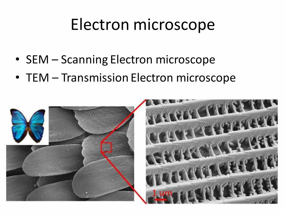
Electron microscope
• SEM – Scanning Electron microscope
• TEM – Transmission Electron microscope

History of electron microscope
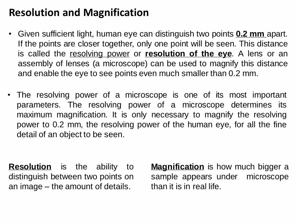
Resolution and Magnification
• Given sufficient light, human eye can distinguish two points 0.2 mm apart.
If the points are closer together, only one point will be seen. This distance
is called the resolving power or resolution of the eye. A lens or an
assembly of lenses (a microscope) can be used to magnify this distance
and enable the eye to see points even much smaller than 0.2 mm.
• The resolving power of a microscope is one of its most important
parameters. The resolving power of a microscope determines its
maximum magnification. It is only necessary to magnify the resolving
power to 0.2 mm, the resolving power of the human eye, for all the fine
detail of an object to be seen.
Magnification is how much bigger a
sample appears under microscope
than it is in real life.
Resolution is the ability to
distinguish between two points on
an image – the amount of details.
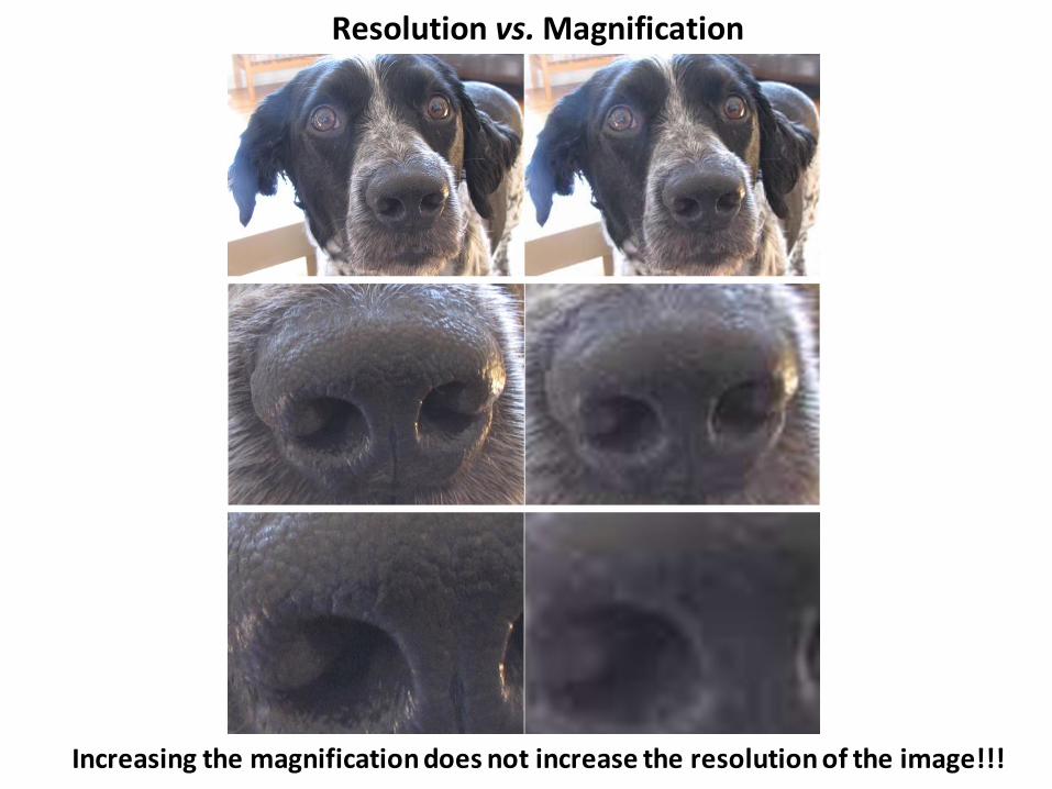
Increasing the magnification does not increase the resolution of the image!!!
Resolution vs. Magnification

Resolution limit (d):
𝑑 =λ
2𝑛 sin 𝛼
λ: wavelength n: refraction index 𝛼: aperture angle of lens dmax: approx. 200 nm
Resolution limit

Light microscope: photons
• A modern light microscope (LM) has a
magnification of about 1000x and enables
eye to resolve objects of 0.0002 mm.
• The resolving power of microscope was
not only limited by the number and quality
of lenses but also by the wavelength of
the light used for illumination.
• Two ways to improve LM resolution:
Using light with a short wavelength (blue or
ultraviolet) gave a small improvement;
immersing samples and the front of the
objective lens in a medium with a high
refractive index (oil) gave another small
improvement.
But, these measures together only brought
the resolving power of microscope to just
under 100 nm.

Why use electrons instead of photons?
• In 1920s it was discovered that accelerated electrons behave in vacuum just like light: travel in straight lines with a wavelength of ~ 100,000 times smaller than that of light.
• Also found that electric and magnetic fields have the same effect on electrons as glass lenses and mirrors have on visible lights.
• Dr. Ernst Ruska at Uni-Berlin combined these characteristics, built the first TEM in 1931. For this and following work, he was awarded the Nobel Prize for Physics in 1986.
• The 1st electron microscope used 2 magnetic lenses and 3 years later he added a third lens and demonstrated a resolution of 100 nm, twice as good as that of the light microscope.
• Today, using 5 magnetic lenses in the imaging system, a resolving power of 0.1 nm at magnifications of over 1 million times can be achieved.
Ernst Ruska Electron Microscope Deutsches Museum - München

From photons to electrons
10 μm
1 μm

Transmission Electron Microscope (TEM) TEM can be compared with a slide projector
• Slide projector: light from a light source is made into a parallel beam by the condenser lens; and passes through the slide (object) and is then focused as an enlarged image onto the screen by the objective lens.
• TEM: light source replaced by electron source (W filament heated in vacuum), glass lenses replaced by magnetic lenses, projector screen replaced by fluorescent screen (emits light when hit by electrons). Beam from source to screen is under vacuum and sample (object) has to be very thin allowing electrons to penetrate it.

Electron gun
Vacuum lock
Sample/Chamber
lens system
CCD camera/ fluorescent screen
Philips TECNAI in Feynmanbau
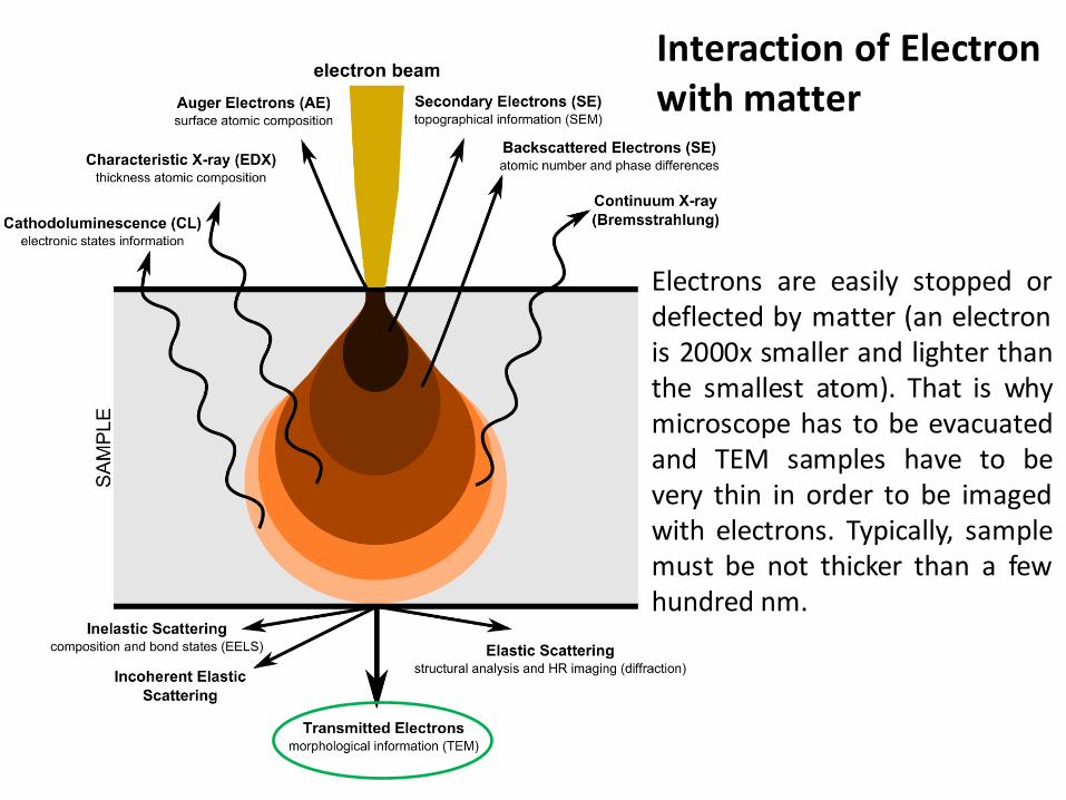
Interaction of Electron with matter
Electrons are easily stopped or deflected by matter (an electron is 2000x smaller and lighter than the smallest atom). That is why microscope has to be evacuated and TEM samples have to be very thin in order to be imaged with electrons. Typically, sample must be not thicker than a few hundred nm.
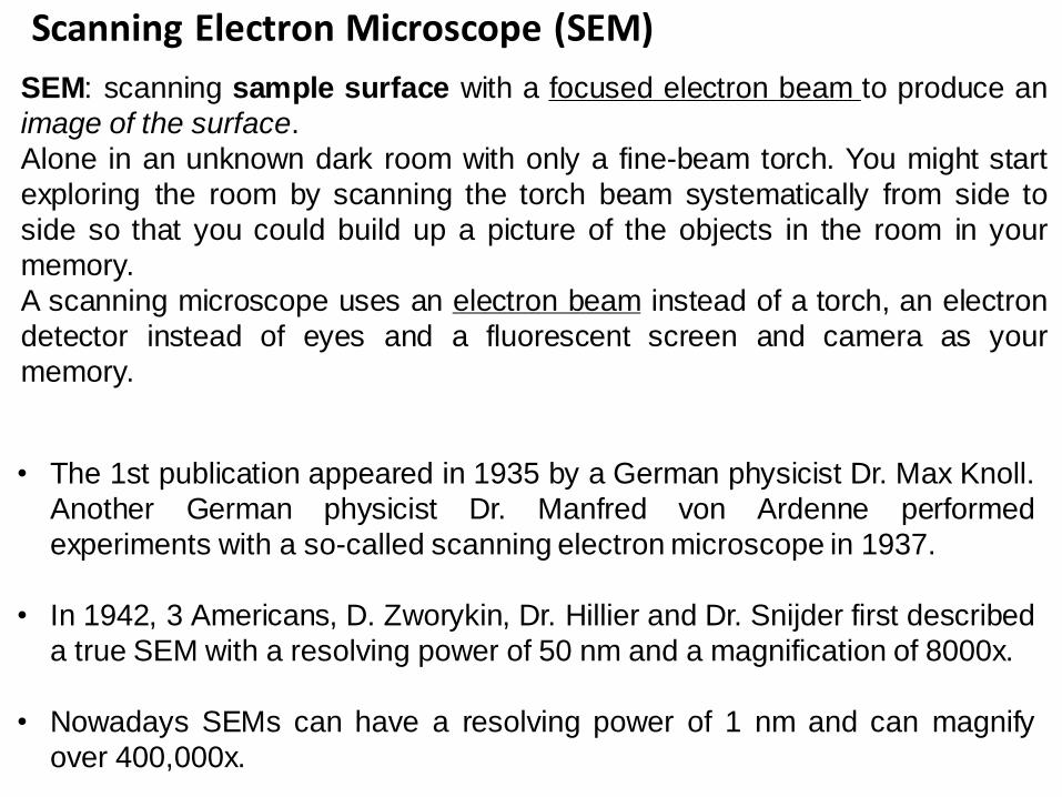
Scanning Electron Microscope (SEM)
SEM: scanning sample surface with a focused electron beam to produce an
image of the surface.
Alone in an unknown dark room with only a fine-beam torch. You might start
exploring the room by scanning the torch beam systematically from side to
side so that you could build up a picture of the objects in the room in your
memory.
A scanning microscope uses an electron beam instead of a torch, an electron
detector instead of eyes and a fluorescent screen and camera as your
memory.
• The 1st publication appeared in 1935 by a German physicist Dr. Max Knoll.
Another German physicist Dr. Manfred von Ardenne performed
experiments with a so-called scanning electron microscope in 1937.
• In 1942, 3 Americans, D. Zworykin, Dr. Hillier and Dr. Snijder first described
a true SEM with a resolving power of 50 nm and a magnification of 8000x.
• Nowadays SEMs can have a resolving power of 1 nm and can magnify
over 400,000x.

History of electron microscope

Comparison of light microscope with TEM and SEM
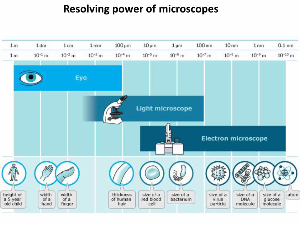
Resolving power of microscopes

TEM
The entire electron path from gun to screen has to be under vacuum (otherwise electrons collide with air molecules and be absorbed). An important difference: unlike glass lenses, electromagnetic lenses are variable: changing the current through lens, focal length (which determines magnification) can be adjusted.

The electron gun
Electron gun has: a filament, a
cylinder & an anode, forming a gun
with a very stable source of
electrons.
Tungsten filament heated to about
2700 ⁰C. By applying a very high
positive potential between filament
and anode, electrons are extracted
from the filament and accelerated
towards the anode.
Anode has a hole so that electron
beam is travelling at a very high
speed (~ 100000 km/s) emerges at
the other side. The higher the
electron speed (the higher the
accelerating voltage in gun), the
thicker the sample being studied.
Beam from gun is condensed into a nearly parallel beam by the condenser lenses and, after passing through sample, projected as a magnified image of sample on fluorescent screen at the bottom of the column.
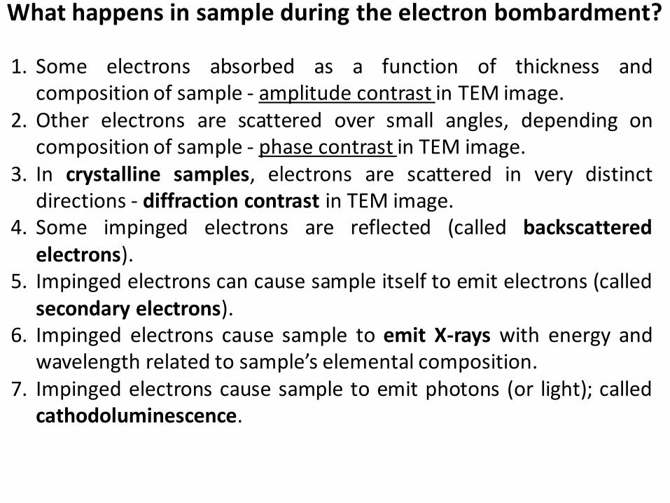
What happens in sample during the electron bombardment?
1. Some electrons absorbed as a function of thickness and composition of sample - amplitude contrast in TEM image.
2. Other electrons are scattered over small angles, depending on composition of sample - phase contrast in TEM image.
3. In crystalline samples, electrons are scattered in very distinct directions - diffraction contrast in TEM image.
4. Some impinged electrons are reflected (called backscattered electrons).
5. Impinged electrons can cause sample itself to emit electrons (called secondary electrons).
6. Impinged electrons cause sample to emit X-rays with energy and wavelength related to sample’s elemental composition.
7. Impinged electrons cause sample to emit photons (or light); called cathodoluminescence.

• Morphology - size, shape, arrangement of particles - atomic diameters;
• Crystalline information - from diffracted electrons, get arrangement
and order of atoms & detection of atomic-scale defects;
• Composition information - Chemical identity (distinguish Fe2+ and
Fe3+ for instance).
What information can be obtained with TEM?
Vellacheri R., Zhao H.P., Mühlstädt M., Ming J., Al-Haddad A., Wu M.H., Jandt K.D., Lei Y.*, ‘All-solid-state cable-type supercapacitors with ultra-high rate capability’, Advanced Materials Technologies, 1 (1), (DOI: 10.1002/admt.201600012), 2016.
TEM images of TiO2 nanotubes
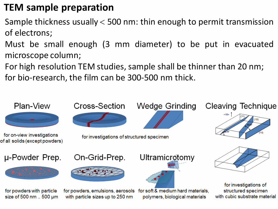
TEM sample preparation
Sample thickness usually 500 nm: thin enough to permit transmission of electrons; Must be small enough (3 mm diameter) to be put in evacuated microscope column; For high resolution TEM studies, sample shall be thinner than 20 nm; for bio-research, the film can be 300-500 nm thick.
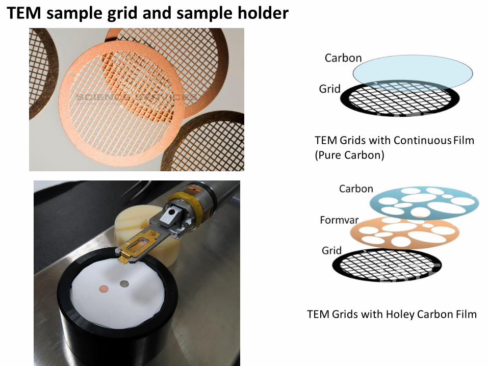
TEM Grids with Holey Carbon Film
TEM Grids with Continuous Film (Pure Carbon)
TEM sample grid and sample holder
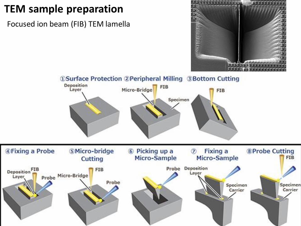
TEM sample preparation Focused ion beam (FIB) TEM lamella
SEM
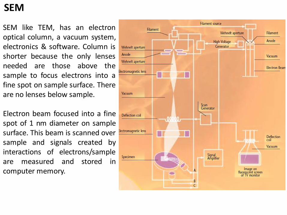
SEM like TEM, has an electron optical column, a vacuum system, electronics & software. Column is shorter because the only lenses needed are those above the sample to focus electrons into a fine spot on sample surface. There are no lenses below sample. Electron beam focused into a fine spot of 1 nm diameter on sample surface. This beam is scanned over sample and signals created by interactions of electrons/sample are measured and stored in computer memory.

SEM Hitachi S4800 im Feynmanbau

What happens in sample during the electron bombardment?
1. The sample itself emits secondary
electrons (SE).
2. Some of the primary electrons are reflected
(backscattered electrons, BSE).
3. Electrons are absorbed by the sample.
4. Sample emits X-rays.
5. Sample sometimes emits photons (= light).
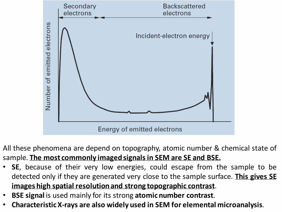
All these phenomena are depend on topography, atomic number & chemical state of sample. The most commonly imaged signals in SEM are SE and BSE. • SE, because of their very low energies, could escape from the sample to be
detected only if they are generated very close to the sample surface. This gives SE images high spatial resolution and strong topographic contrast.
• BSE signal is used mainly for its strong atomic number contrast. • Characteristic X-rays are also widely used in SEM for elemental microanalysis.

Cross-section BSE image, showing pore opening, pore wall, and SnO2 layer. Al2O3 membrane and SnO2 show different contrast. SnO2 is brighter compared to Al2O3 because of higher z-value (50:13).
Cross-section SE-SEM image, showing UTAM filled with SnO2. The present of 2 different materials can not be observed clearly. BSE detection proves the existence of 2 materials.
SE and BSE modes in a SEM

Magnification and resolution in a SEM
Magnification determined by electronic circuit scanning the beam over the sample (and over the fluorescent screen of monitor). Increasing magnification is achieved by reducing the size of the area scanned on sample. Magnification can be as high as 300,000x which is usually more than sufficient.
Resolution of a SEM is determined by beam diameter on sample surface. The practical resolution depends on the properties of sample and sample preparation technique and on many instrumental parameters: beam intensity, accelerating voltage, scanning speed, distance from the last lens to sample (usually referred to as the working distance) and the angle of sample surface to the detector. Under optimum conditions a resolution of 1 nm can be attained.


Electron Sources in a SEM - Thermionic Sources Tungsten Filament LaB6
Thermionic electron source for SEM
Major Advantages: • Very high probe currents • Stable probe, especially W • Less complex vacuum system • Lowest overall cost / easy to maintain Disadvantages: • Lower brightness • Relatively short lifetimes

Electron Sources in a SEM - Cold Field Emission Sharp Single Crystal (310) Tungsten Tip
Major Advantages: • Highest brightness SEM source available • Very long potential source lifetime – many years Disadvantages: • Lowest maximum probe current • Poor short and long term probe current stability • Requires ultra-high vacuum in gun area • Cost (initial)

Electron Sources in a SEM - Thermal-Field (Schottky) Emission
Sharp Single Crystal (100) Tungsten Tip with Zr02 (zirconium oxide) Film
Major Advantages: • Very high brightness source • High probe currents obtainable (few hundred nA) • Long potential source lifetime (few years) • Excellent short and long term stability Disadvantages: • Requires ultra-high vacuum in gun area • Source heating is continuous, 24/7 (finite life) • Cost (initial and maintenance)

Comparison of Electron Sources in a SEM
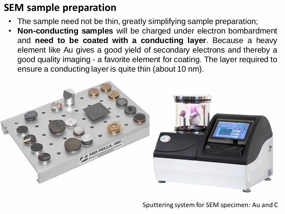
• The sample need not be thin, greatly simplifying sample preparation;
• Non-conducting samples will be charged under electron bombardment
and need to be coated with a conducting layer. Because a heavy
element like Au gives a good yield of secondary electrons and thereby a
good quality imaging - a favorite element for coating. The layer required to
ensure a conducting layer is quite thin (about 10 nm).
SEM sample preparation
Sputtering system for SEM specimen: Au and C

Elemental analysis based on “Characteristic X-rays”
When electrons in inner shells are emitted from atoms due to irradiation of incident electrons, the vacant orbits are filled with outer-shell electrons, and sample emits X-ray with energies correspond to the energy difference between outer-shell and inner-shell electrons. These X-rays called “Characteristic X-rays” because their energies (wavelength) are characteristic of individual elements. Thus, the characteristic X-rays are used for elemental analysis. Characteristic X-rays that are emitted by excitation of electrons in K shells are called “K lines”, those emitted by L and M shell excitations called “L lines” and “M lines”.

Elemental analysis in SEM: EDS
Energy Dispersive X-ray Spectrometer (EDS) is used to analyze characteristic X-ray spectra by measuring the energies of X-rays.
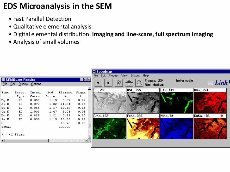
EDS Microanalysis in the SEM
• Fast Parallel Detection • Qualitative elemental analysis • Digital elemental distribution: imaging and line-scans, full spectrum imaging • Analysis of small volumes

EDS Full Spectrum Imaging
A full X-ray spectrum: elemental maps, phase maps, and quantitative analysis extracted from full spectrum images.
Cumulative Spectra and Quantitative Analysis for each extracted phase

Example of EDS Microanalysis in the SEM
Wen L.Y., Xu R., Mi Y., Lei Y.*, ‘Multiple nanostructures based on anodized aluminium oxide templates’, Nature Nanotechnology, 12, 244 (2017).
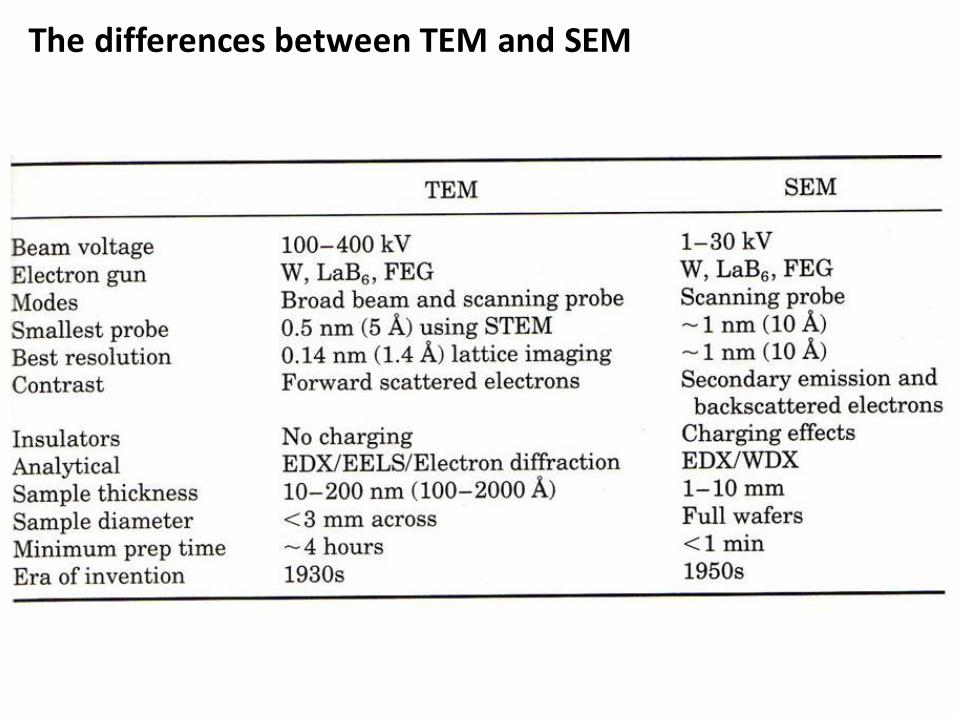
The differences between TEM and SEM

Low energy electron diffraction (LEED): crystallography of surface and interfaces
A mono-energetic electron beam is directed on a single crystal surface and diffraction pattern of elastic back-scattered electrons is recorded. Like all wave-like objects, the angular intensity distribution due to the interference of partial waves back-scattered from a periodic array is described by Bragg’s law, which predict a regular pattern of diffraction spots.
Experimental LEED patterns formed by CO adsorbed on Ni{111} (left) and corresponding real-space unit cells (right)

Reflection high-energy electron diffraction (RHEED): used in MBE (molecular beam epitaxy)
Reflection high-energy electron diffraction (RHEED) uses a finely parallel electron beam with energy of 10–100 keV. The beam irradiates a sample surface with grazing incidence to obtain forward scattered diffraction patterns. RHEED enables us to analyze structures of crystal surfaces at atomic levels and also to in situ monitor growth processes of thin films.

PED is a specialized method to collect electron diffraction patterns in TEM. By rotating a tilted incident electron beam around the central axis of microscope, a PED pattern is formed by integration over a collection of diffraction conditions. This produces a diffraction pattern to determine the crystal structure of the sample.
wikipedia
Precession electron diffraction (PED)

Thanks for listening!