technology, performance and degradation characteristics of ... · technology, performance and...
TRANSCRIPT
FACTA UNIVERSITATIS Series: Electronics and Energetics Vol. 26, No 3, December 2013, pp. 247 - 280 DOI: 10.2298/FUEE1303247M
TECHNOLOGY, PERFORMANCE AND DEGRADATION
CHARACTERISTICS OF SLS ELA THIN FILM TRANSISTORS
Despina C. Moschou1, Dimitrios N. Kouvatsos
1,
Giannis P. Kontogiannopoulos1, Filippos V. Farmakis
1,
Apostolos T. Voutsas2
1Institute of Advanced Materials, Physicochemical Processes, Microsystems
and Nanotechnology, NCSR "Demokritos", 153 10 Aghia Paraskevi, Greece 2Material and Device Applications Laboratory, Sharp Labs of America, Camas, WA 98607,
USA
Abstract. Low temperature polycrystalline silicon thin film transistors (LTPS poly-Si
TFTs) are essential for large area electronics and high performance flat panel displays.
In recent years, LTPS TFT performance has substantially increased due to the
important breakthroughs in the field of polycrystalline silicon crystallization and also
due to the optimization of the process steps that differ from those of typical MOSFETs,
mainly because of the requirement for low temperature procedures. In this review we
present the electrical characteristics of polycrystalline silicon TFTs, crystallized with
different variations of the advanced SLS ELA technique, and the determination of
process technological parameters that affect the device performance, in order to further
optimize the production of such high performance transistors, in terms of poly-Si
microstructure, channel dimensions and topology. Also, the effect of these fabrication
parameters on device degradation characteristics is studied, with an attempt to model and
predict degradation characteristics.
Keywords: TFT, SLS ELA, poly-Si, LTPS, crystallization, degradation
1. INTRODUCTION
Polycrystalline silicon thin film transistor (TFT) technology is critically important for
large area electronics, particularly for flat panel active matrix liquid crystal display appli-
cations (AMLCDs), and for high density static random access memory (SRAM) circuits
[1]. In particular, low temperature polysilicon (LTPS) TFTs have been intensively
investigated because they can be used for integrating driving circuits and pixel elements
on a common substrate in flat panel displays for realizing systems on panel (SOP). This is
the case because LTPS TFTs have much higher electron mobility and drive current com-
Received December 20, 2013 Corresponding author: Dimitrios N. Kouvatsos
Institute of Advanced Materials, Physicochemical Processes, Microsystems and Nanotechnology, NCSR "Demokritos", 153 10 Aghia Paraskevi, Greece
(e-mail: [email protected])

248 D. MOSCHOU, D. KOUVATSOS, G. KONTOGIANNOPOULOS, F. FARMAKIS, A. VOUTSAS
pared with amorphous-Si TFTs (a-Si) [2-4]. However, these advantages could not be
fully realized in the early days of LTPS TFT technology, when solid phase crystallization
(SPC) was the means of acquiring the polysilicon films; due to low-temperature processes
that have to be used for glass substrates, numerous defects in poly-Si grains and at grain
boundaries exist and degrade device characteristics. In recent years, these issues have been
mainly overcome by using a variety of advanced crystallization processes that have been
developed, such as sequential lateral solidification excimer laser annealing (SLS ELA) [2-
4]. Utilizing such techniques, it is now possible to fabricate polysilicon TFTs of very high
active layer quality, suitable for system on panel applications.
In this paper, we present results on the performance and reliability characteristics of
LTPS TFTs obtained through various innovative SLS ELA techniques. We first briefly
discuss the development of laser annealing techniques, which have yielded breakthroughs
in polysilicon film quality, and then we particularly describe the SLS ELA method. Sub-
sequently, in the experimental section we describe the particular SLS ELA techniques
used, the TFT fabrication process and the electrical measurements for extraction of de-
vice parameters and characteristics for performance and reliability investigation. The SLS
ELA methods we have utilized yield polycrystalline silicon grains with engineered
shapes, which can be and very elongated, thus resulting in TFTs exhibiting very high
performance. Moreover, they also allow the fabrication of TFTs with channels oriented in
parallel or vertically to the grain boundaries, thus affording more control on TFT charac-
teristics. In addition, the TFT structure and geometry has significant effects on device
performance and reliability, which are investigated. Advanced device structures such as
double gates offer additional flexibility for tailoring TFT electrical characteristics to
achieve enhanced performance.
2. POLYSILICON CRYSTALLIZATION
2.1. Basic features of laser annealing techniques
Laser anneal crystallization techniques constitute a radical departure from earlier,
thermal furnace based, SPC methods; they allowed TFT fabrication to overcome thermal
budget constraints posed by the glass substrates and achieve drastically improved active
layer film quality. A particular type of laser called excimer is mostly used for the crystal-
lization of amorphous silicon (a-Si) films, in a process called Excimer Laser Crystalliza-
tion (ELC) or Excimer Laser Anneal (ELA). These lasers use stimulated radiation from
excimer molecules (each consisting of a noble gas and a halogen gas atom) in the ultravi-
olet range, which is very strongly absorbed by amorphous silicon; for silicon crystalliza-
tion ArF, KrF, XeCl and XeF are used, emitting laser light of wavelength 193 nm, 248
nm, 308 nm and 351 nm, respectively. The incident laser energy is mostly absorbed
within the first atomic layers (6-10 nm thick) of the silicon film, thus causing rapid heat-
ing and melting of the film. XeCl, emitting at 308 nm, is the excimer laser most com-
monly used, because at this wavelength a-Si absorbs radiation very strongly, while the
cost and lifetime of relevant optics are suitable for mass production. Typical XeCl laser
pulses have frequency of around 300 Hz and duration of 10 to 50 ns.
ELC of a-Si films can be classified in different crystallization regimes depending on
the incident laser energy [5], a low energy (A), a high energy (C) and an intermediate
energy one (B) (Fig. 1). In the first case, the laser energy is sufficient to only partially

Technology, Performance and Degradation Characteristics of SLS ELA Thin Film Transistors 249
melt the silicon film, while in the second one the energy is high enough for full melting.
Within a narrow process window in between lies the intermediate regime, which corre-
sponds to the situation of superlateral growth (SLG). This is a mechanism of great tech-
nological importance, as the polysilicon film formed has grains significantly larger than
the film thickness. In this case, we have near-complete melting in which there are discrete
islands of still solid material under the molten silicon, separated by fully melted material.
These solid islands constitute crystallization seeds, from which lateral crystal growth
within the surrounding molten silicon commences. Conventional ELC aims at near-com-
plete melting for SLG and, via repeated irradiations, increase of size and uniformity of
the grains. Multiple irradiations may use some overlap, between shots, in the exposed
area; the number of shots and the overlap width are determined by film quality and
throughput considerations.
Fig. 1 The three crystallization mechanisms related to the laser irradiation energy
The solidified films exhibit surface roughness, localized at the grain boundaries and
formed due to density differentials between molten and solid silicon. As molten silicon
solidifies, it expands. Crystal growth begins at seeds and the last molten material lies
between growth fronts; when they collide, the newly solidified silicon can only expand
upwards, resulting in protuberances associated with the grain boundaries formed. The
resulting ELC polycrystalline silicon films are of much higher quality than furnace an-
nealed SPC films. They exhibit much lower densities of intragrain defects, a factor much
more important than the larger grain size also afforded by ELC. A disadvantage, how-
ever, is the difficulty of striking an optimum balance between film quality and
uniformity. Furthermore, as the grain size in ELC films is comparable to TFT channel
lengths, large statistical fluctuations due to grain boundaries may result. For short channel

250 D. MOSCHOU, D. KOUVATSOS, G. KONTOGIANNOPOULOS, F. FARMAKIS, A. VOUTSAS
lengths (e.g. <0.5 μm) we may have channels within a single grain, but the location of
grain boundaries with respect to TFT channels would have to be precisely controlled.
Several advanced ELC techniques have been proposed in recent years for optimum
crystallization in order to tackle these issues [6].
The basic issue driving the development of advanced ELC techniques is the manipu-
lation of the intrinsically unstable condition of superlateral growth in such a way as to
allow for controllable engineering of the final film microstructure. In this sense, all these
techniques can be grouped under the term "controlled SLG" (C-SLG). By controlling the
shape and dimensions of areas being melted via several optical, photolithographic and
other methods, C-SLG techniques can tailor the resulting film microstructure so as to
yield controlled, predictable and uniform grain size and structure. This is a direct result of
the relationship between the distance of lateral growth and the width of the irradiated
area. The lateral growth distance is limited by the onset of nucleation inside the molten
material or by the collisions of crystallization fronts growing from opposite sides of the
molten area. By suitably selecting the width of the molten area formed by the laser irradi-
ation in relation to the lateral growth distance nucleation events can be severely sup-
pressed (Fig. 2). In this way, a very uniform film structure consisting of very elongated
grains can be achieved over large areas [7]. Many techniques can be suitable for
preselecting the areas that will be fully melted; these include silicon film thickness varia-
tion, coating of the a-Si film with a preformed antireflective film and projection shaping
of the laser beam profile [8].
2.2. SLS ELA crystallization
Fig. 2 Superlateral growth (left) and controlled superlateral growth (right) of silicon crystals
One of the excimer laser annealing techniques that yields impressive results is se-
quential lateral solidification (SLS) [9]. In this technique laterally developed crystals
(Fig. 2) can be elongated to vary large horizontal dimensions. This is accomplished by
Technology, Performance and Degradation Characteristics of SLS ELA Thin Film Transistors 251
shifting the sample in respect to the laser beam or shifting the beam in respect to the sam-
ple. If the shifting distance is shorter than the distance of superlateral growth, the Si film
can be re-molten in such a way that the molten region is in contact to a part of the later-
ally developed grains from the previous step. This technique gives vary large grains of
excellent intragrain quality (comparable to silicon on insulator-SOI), allowing the fabri-
cation of devices within each of these optimum quality grains. By implementing the
channel region within the high-quality crystallite, we avoid including in the channel re-
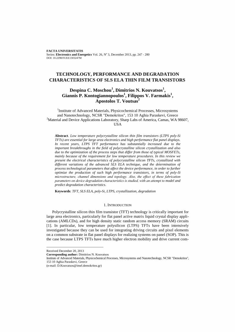
gion grain boundaries, which cause electron and hole energy barriers (Fig. 3) that are
responsible for lower effective mobility values in transistors [10].
Fig. 3 Effect of grain boundaries in the silicon energy diagram
3. EXPERIMENTAL
Since SLS ELA Si quality depends in the shifting of the sample in respect to the laser
beam, several techniques can be employed in this direction, resulting in different crystal
arrangements, crystallite dimensions and geometry. Scanning electron microscopy (SEM)
images of the resulting films for each technique can reveal these characteristics,
subsequently related to the electrical performance of the devices fabricated in them.
252 D. MOSCHOU, D. KOUVATSOS, G. KONTOGIANNOPOULOS, F. FARMAKIS, A. VOUTSAS
Fig. 4 SEM images of the differently crystallized polysilicon films
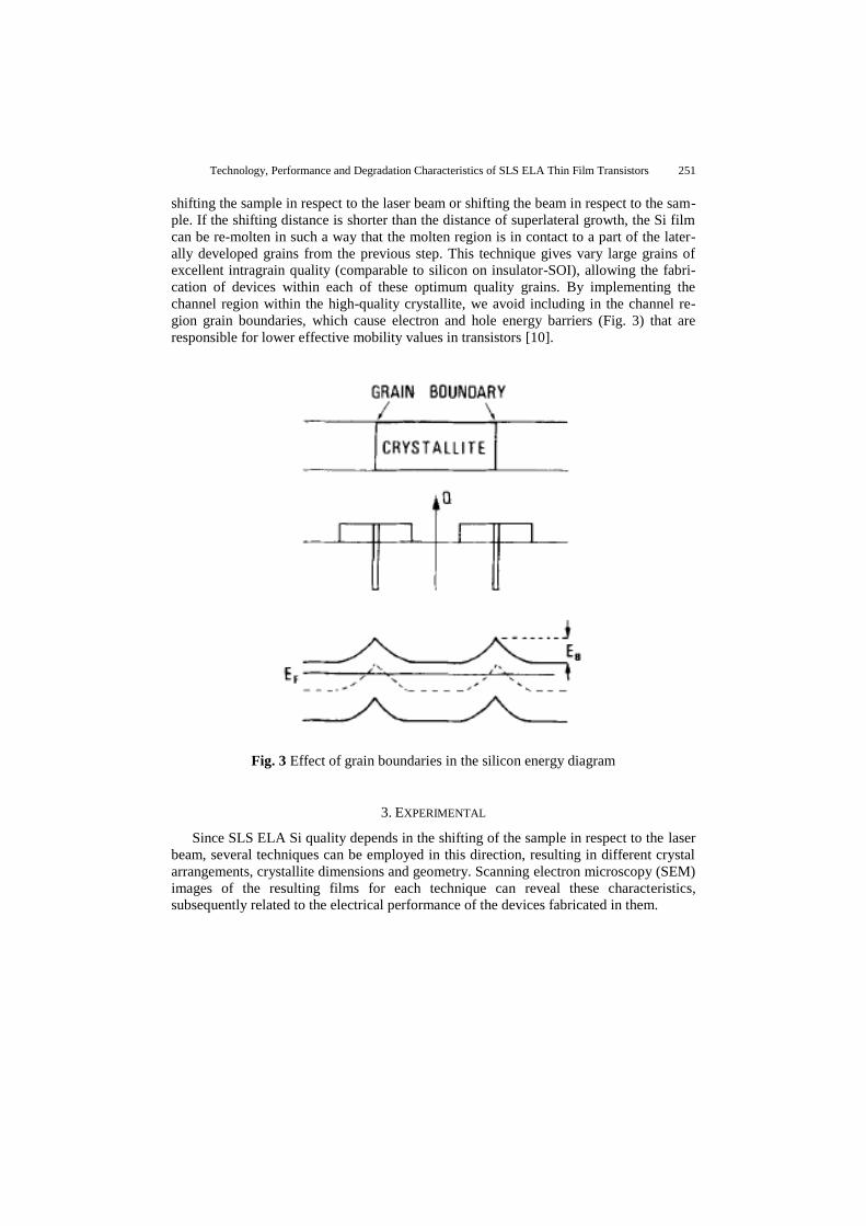
In Fig. 4 we can see SEM images of the SLS ELA polysilicon films to be studied: di-
rectional [11], seeded directional [12], 22-shot [13], 2
6-shot [13], M×N shot [13] of differ-
ent crystal dimensions, dot hexagonal and square crystallization [13]. All these tech-
niques vary in the shape of the laser mask used with all other process parameters kept to
the optimized values (i.e. room temperature, excimer laser wavelength, frequency etc). In
directional crystallization films are crystallized with the laser beam shaped through a one
rectangular slit (25μm wide). This rectangular laser beam melts the film locally and is
then shifted to melt the adjacent region. In this way the whole film area is scanned, re-
sulting in a film of many elongated and roughly parallel grains. In the seeded version, the
laser mask is the same, but within the original film there are some crystal seeds at
specific points, acting as the crystallization onsets. The result is radial grain boundaries,

Technology, Performance and Degradation Characteristics of SLS ELA Thin Film Transistors 253
following the crystal structure of the original seed. In the 2-shot technique the laser mask consists of two columns with parallel slits, slightly offset with each other. For 2N-shot techniques (in our case N = 2 or 6) the laser beam is split in a number of regions, each consisting of parallel slit sets, vertical to each other. Half of the N regions are x oriented and the other half are y oriented, again slightly offset with each other. The M×N technique is a variation of the previous one, with M slits in the x direction and N slits in the y direction.
Fig. 5 AFM images of the SLS ELA crystallized samples studied
Apart from the slit approach for shaping the laser mask, there is also the approach of dot array masks of appropriate geometry. In this case crystallization begins from the dot points and proceeds radially. The distance and geometry of the dots now defines the mi-crostructure of the crystallized polysilicon. In our case, when the dots are arranged in a square array we form squarer grains and when they are arranged in a hexagonal array we get hexagonal grains.
In order to see the effect of crystallization techniques in the surface roughness of the films, we also characterized them through atomic force microscopy (AFM) [14], as pre-sented in Fig. 5. As we can see, the larger the shot number in a film the larger the pol-ysilicon protrusions observed and the larger the film surface roughness. Also, for M×N and dot crystallized films, where the intragrain quality is lower due to the sub-boundaries present (see SEM images of Fig. 4), film protrusions are more sparse and located mainly in the grain boundaries.

254 D. MOSCHOU, D. KOUVATSOS, G. KONTOGIANNOPOULOS, F. FARMAKIS, A. VOUTSAS
After the morphological characterization of the differently crystallized polysilicon
films, TFTs were fabricated in them. We fabricated top gate [12], bottom gate [12] and
double gate [15] devices, oriented in both the x and y direction of the films, since we saw
that grains and grain boundaries are different with respect to the film orientation. The top
gate insulator was a 30 nm thick PECVD SiO2 and the bottom gate insulator was a 50 nm
thick PECVD SiO2. Different channel widths W and lengths L were studied, ranging
from W = 1 μm – 100 μm and L = 0.5 μm – 4 μm.
The Id – Vg TFT transfer characteristics were measured, utilizing a HP4140B semi-
conductor analyzer and a Keithley voltage source in a dark box under no illumination, in the
linear region, with Vd = 0.1 V. For the double gate TFTs, their transfer characteristics were
recorded varying the bottom gate bias Vgb from –3 V to 3 V. The maximum of the slope of
the Id – Vg characteristic, drawn in linear scale, yields the maximum transconductance
Gm,max at a particular gate bias Vg,max. The intercept, with the horizontal axis, of a straight
line with that slope, fitted to the characteristic at Vg,max yielded the extrapolated threshold
voltage Vth. Also, the subthreshold slope for all measured devices was calculated.
For the degradation studies we conducted, the TFT structures were dc stressed, bias-
ing appropriately the gate(s) and drain for a predefined stress time for each step, accord-
ing to the stress condition selected for each experiment (see following paragraphs for
details). After each cycle the Id – Vg characteristics were measured in the linear region
with Vds = 0.1 V and their electrical parameters (Vth, Gm,max and S) were calculated.
4. RESULTS & DISCUSSION
4.1. Characterization Results
4.1.1. Crystallization effects on TFT electrical parameters
In Table 1 [13] we can see the average values of the threshold voltage Vth, the field-
effect mobility μ and the subthreshold slope S of the measured TFTs. We examined two
different variations of the Dot technology and three different variations of the MN one,
the only differences being (i) for the Dot technologies, the hexagonal dot matrix for the
30HEX samples vs. the square dot matrix for 50SQ ones, and (ii) for the MN technolo-
gies, the crystal domain size.
As far as S is concerned, we can see that it appears to be increased for the samples
having an increased number of grain boundaries within the channel area , with the sole
exception of the Dot TFTs, where we would normally expect it to be higher, since it has
the worst polycrystalline quality. This can be explained if we consider the effect of what
kind of traps is reflected on each parameter. We know that through S midgap traps,
mainly located in intragrain areas, can be probed. Therefore, the small S value of the Dot
TFTs, considering the rather increased number of grain boundaries, can be attributed to
more tail-states existing for that technology than midgap ones.
So, comparing the mean μ value of the TFTs crystallized with different technologies,
we can see that the largest mobility values, approaching the single-crystalline reference
one of SIMOX, are obtained for MN TFTs, followed closely by 2-shot TFTs and then
by 26-shot and Dot ones. This order of these different technologies with decreasing mo-
bility can be attributed to two factors: the grain-boundary trap density and the surface

Technology, Performance and Degradation Characteristics of SLS ELA Thin Film Transistors 255
roughness, causing more pronounced carrier surface scattering and therefore degrading
device field effect mobility.
Considering these two factors, we see that the MN TFTs, having the largest mobility
values, indeed have the fewer grain boundaries of all and, at the same time, the less pro-
nounced surface roughness. The next lowest value of grain boundaries is that for the 26-
shot sample, showing its very good polysilicon quality, also observed from the SEM im-
age. Nevertheless, its mobility is lower than that of the 2-shot sample, having a similar
crystal structure. This is because of the extremely pronounced roughness observed in the
26-shot sample, as compared to the 2-shot one. Finally, the Dot TFTs having the largest
number of grain boundaries, despite their small surface roughness, exhibit the smallest
mobilities of all devices. Therefore, low grain boundary densities within the channel area
are essential to obtain large field-effect mobility, but the effect of surface roughness
should not be neglected, since it can substantially degrade the performance of a TFT.
Table 1 Device parameter statistics for different crystallization techniques
Vth (V) μ (cm2/V∙sec) S (mV/decade)
MEAN STD MEAN STD MEAN STD
SIMOX -0.57 0.46 322.15 42.92 0.11 0.01
2-shot -1.87 0.56 282.31 67.02 0.39 0.25
26-shot 0.21 0.23 187.33 62.83 0.16 0.03
Dot 30HEX -1.31 0.28 163.01 37.97 0.23 0.04
50SQ 0.62 0.37 198.14 18.99 0.21 0.02
MN #1 -1.03 0.38 235.40 55.23 0.17 0.03
#7 -0.95 0.29 321.96 26.50 0.19 0.05
#8 -0.20 0.48 289.08 36.03 0.15 0.02
4.1.2. Vg,max – Vth parameter importance
After measuring the Id – Vg characteristics of our top gate TFTs, we extracted their
field effect mobility μ and the threshold voltage Vth. We, also, calculated graphically
(Fig. 6), the difference Vg,max – Vth for each device [16]; Vg,max is the value of the gate
voltage at which the maximum transconductance is observed.
In table 2 we can see their values for 5 different TFTs. A comparison between TFTs
with their channels oriented vertical to grain boundaries and parallel to them shows much
lower μ values for the former (A vs B and E vs D), since the grain boundaries are known
to reduce the carrier mobility. However, Vth does not seem to be as affected just by the
channel orientation (A vs B and E vs D). Other technological parameters, such as oxide
trapped charges and interface charges, are known to affect the Vth value in a more pro-
nounced manner. Observing the third parameter Vg,max – Vth of the table, we see that its
value is also not as strongly dependent on channel orientation as the carrier field effect
mobility μfe (A vs B). Nevertheless, this parameter does not seem to follow exactly the
same behavior as Vth (C vs D and D vs E). Also, we see that while devices B, C and D
have decreasing μfe the same pattern is not followed by the parameter Vg,max – Vth alt-
hough theoretically both parameters depend on poly-Si traps. However, it is known that
the field effect mobility is strongly dependent on the lateral field distribution and there-
fore reflects more factors than Vg,max – Vth (a parameter "seeing" the device on the verti-

256 D. MOSCHOU, D. KOUVATSOS, G. KONTOGIANNOPOULOS, F. FARMAKIS, A. VOUTSAS
cal electrical field direction), such as channel orientation with respect to the grain bound-
aries and surface scattering of carriers.
Fig. 6 Graphic representation of the difference of the extrapolated threshold voltage Vth
and the voltage bias for maximum transconductance Vg,max (Vg,max Vth)
Table 2 LTPS TFT electrical parameters
TFT name Grains vs
channel
Field effect mobility
μfe
(cm2/V·sec)
Vth
(V)
Vg,max Vth
(V)
A ┴ 38 0.22 0.48
B // 145 0.24 0.46
C // 137 0.53 0.57
D // 101 0.93 0.57
E ┴ 31 0.94 1.26
Therefore, from our previous analysis, we could say that the three studied electrical
parameters seem to be independent from each other, each one reflecting different tech-
nological parameters: Vth is known to reflect mostly interface traps and oxide charges,
while Gm,max (and μfe) reflects polysilicon traps obstructing the current flow and scattering
of the current carriers; Vg,max Vth reflects polysilicon traps irrespective of their effect on drain
current, and specifically tail states, if we consider traps distributed within the band gap.
4.1.3. Grain boundary effects on TFT performance
We extracted the parameters and characteristics of single-shot and overlapping direc-
tional TFTs, oriented in the preferential (X) or the non-preferential (Y) direction [11].
0,0 0,2 0,4 0,6 0,8 1,0 1,2 1,4 1,6 1,8 2,00,0
7,0x10⁻⁵
1,4x10⁻⁴
2,1x10⁻⁴
2,8x10⁻⁴
3,5x10⁻⁴
X direction
Y direction
Ids
-Vgs
I ds(A
)
Vgs
(V)
0,0
2,0x10⁻⁵
4,0x10⁻⁵
6,0x10⁻⁵
8,0x10⁻⁵
1,0x10⁻⁴
1,2x10⁻⁴
1,4x10⁻⁴
1,6x10⁻⁴
1,8x10⁻⁴ X direction
Y direction
Gm-V
gs
Gm(o
hm
-1)
Technology, Performance and Degradation Characteristics of SLS ELA Thin Film Transistors 257
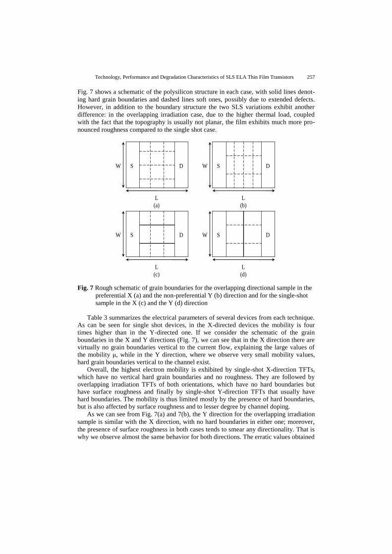
Fig. 7 shows a schematic of the polysilicon structure in each case, with solid lines denot-
ing hard grain boundaries and dashed lines soft ones, possibly due to extended defects.
However, in addition to the boundary structure the two SLS variations exhibit another
difference: in the overlapping irradiation case, due to the higher thermal load, coupled
with the fact that the topography is usually not planar, the film exhibits much more pro-
nounced roughness compared to the single shot case.
Fig. 7 Rough schematic of grain boundaries for the overlapping directional sample in the
preferential X (a) and the non-preferential Y (b) direction and for the single-shot
sample in the X (c) and the Y (d) direction
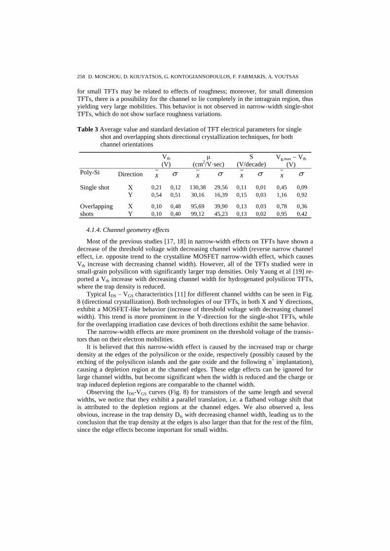
Table 3 summarizes the electrical parameters of several devices from each technique. As can be seen for single shot devices, in the X-directed devices the mobility is four times higher than in the Y-directed one. If we consider the schematic of the grain boundaries in the X and Y directions (Fig. 7), we can see that in the X direction there are virtually no grain boundaries vertical to the current flow, explaining the large values of the mobility μ, while in the Y direction, where we observe very small mobility values, hard grain boundaries vertical to the channel exist.
Overall, the highest electron mobility is exhibited by single-shot X-direction TFTs, which have no vertical hard grain boundaries and no roughness. They are followed by overlapping irradiation TFTs of both orientations, which have no hard boundaries but have surface roughness and finally by single-shot Y-direction TFTs that usually have hard boundaries. The mobility is thus limited mostly by the presence of hard boundaries, but is also affected by surface roughness and to lesser degree by channel doping.
As we can see from Fig. 7(a) and 7(b), the Y direction for the overlapping irradiation
sample is similar with the X direction, with no hard boundaries in either one; moreover,
the presence of surface roughness in both cases tends to smear any directionality. That is
why we observe almost the same behavior for both directions. The erratic values obtained
W S D W S D
W S D W S D
L L
(a) (b)
L L
(c) (d)
258 D. MOSCHOU, D. KOUVATSOS, G. KONTOGIANNOPOULOS, F. FARMAKIS, A. VOUTSAS
for small TFTs may be related to effects of roughness; moreover, for small dimension
TFTs, there is a possibility for the channel to lie completely in the intragrain region, thus
yielding very large mobilities. This behavior is not observed in narrow-width single-shot
TFTs, which do not show surface roughness variations.
Table 3 Average value and standard deviation of TFT electrical parameters for single
shot and overlapping shots directional crystallization techniques, for both
channel orientations
Vth
(V)
μ
(cm2/V·sec)
S
(V/decade) Vg,max Vth
(V)
Poly-Si Direction x x x x
Single shot Χ 0,21 0,12 130,38 29,56 0,11 0,01 0,45 0,09
Υ 0,54 0,51 30,16 16,39 0,15 0,03 1,16 0,92
Overlapping
shots
Χ 0,10 0,48 95,69 39,90 0,13 0,03 0,78 0,36
Υ 0,10 0,40 99,12 45,23 0,13 0,02 0,95 0,42
4.1.4. Channel geometry effects
Most of the previous studies [17, 18] in narrow-width effects on TFTs have shown a
decrease of the threshold voltage with decreasing channel width (reverse narrow channel
effect, i.e. opposite trend to the crystalline MOSFET narrow-width effect, which causes
Vth increase with decreasing channel width). However, all of the TFTs studied were in
small-grain polysilicon with significantly larger trap densities. Only Yaung et al [19] re-
ported a Vth increase with decreasing channel width for hydrogenated polysilicon TFTs,
where the trap density is reduced.
Typical IDS – VGS characteristics [11] for different channel widths can be seen in Fig.
8 (directional crystallization). Both technologies of our TFTs, in both X and Y directions,
exhibit a MOSFET-like behavior (increase of threshold voltage with decreasing channel
width). This trend is more prominent in the Y-direction for the single-shot TFTs, while
for the overlapping irradiation case devices of both directions exhibit the same behavior.
The narrow-width effects are more prominent on the threshold voltage of the transis-
tors than on their electron mobilities.
It is believed that this narrow-width effect is caused by the increased trap or charge
density at the edges of the polysilicon or the oxide, respectively (possibly caused by the
etching of the polysilicon islands and the gate oxide and the following n+ implantation),
causing a depletion region at the channel edges. These edge effects can be ignored for
large channel widths, but become significant when the width is reduced and the charge or
trap induced depletion regions are comparable to the channel width.
Observing the IDS-VGS curves (Fig. 8) for transistors of the same length and several
widths, we notice that they exhibit a parallel translation, i.e. a flatband voltage shift that
is attributed to the depletion regions at the channel edges. We also observed a, less
obvious, increase in the trap density Dts with decreasing channel width, leading us to the
conclusion that the trap density at the edges is also larger than that for the rest of the film,
since the edge effects become important for small widths.

Technology, Performance and Degradation Characteristics of SLS ELA Thin Film Transistors 259
Fig. 8 Normalized IDS-VGS characteristics for several channel widths of TFTs with
channel length L = 1 μm, for single-shot devices oriented in the preferential
direction
Fig. 9 Field-effect mobility μ as a function of channel length L
for M×N crystallized SLS ELA TFTs
As far as the channel length is concerned, in Fig. 9 we can clearly see that the field effect mobility of all of the X oriented devices (M×N crystallization) is significantly larger than that of the Y oriented devices, which supports the DLTS conclusion that in the preferential X direction the process results in better intragrain quality due to "softer" sub-boundaries [20]. For larger or smaller channel lengths than 1.2 μm the performance seems to deteriorate. This optimum length addressing to intermediate L values shows enhanced performance and could be related to the subthreshold slope S of the devices
-3 -2 -1 0 1 2 310
-15
10-14
10-13
10-12
10-11
10-10
10-9
10-8
10-7
10-6
10-5
W=100 m
W=32 m
W=16 m
W=8 m
W=4 m
W=2 m
W=1 m
I ds-n
orm
aliz
ed (
A)
Vgs
(V)
0,4 0,6 0,8 1,0 1,2 1,4 1,6 1,8 2,0 2,2
50
100
150
200
250
X direction W=2m
X direction W=8m
Y direction W=2m
Y direction W=8m
(
cm
2/V
·se
c)
L (m)
260 D. MOSCHOU, D. KOUVATSOS, G. KONTOGIANNOPOULOS, F. FARMAKIS, A. VOUTSAS
[20]. The increasing mobility with increasing L, in the L regime below 1.2 μm, is some-thing expected, since, observing the SEM image, we see that more sub-boundaries are included within the channel region for longer channel lengths. The increase of S with decreasing channel length, in the L regime above 1.2 μm, is an electrical effect, ascribed to the increased channel charge in the subthreshold regime due to the additional drain bias control of the channel region. So the deterioration of the TFT performance for small channel lengths is an electrical effect while the deterioration for large channel lengths is process related. These two mechanisms define the optimum channel length.
4.1.5. Top, bottom and double gate TFT structures
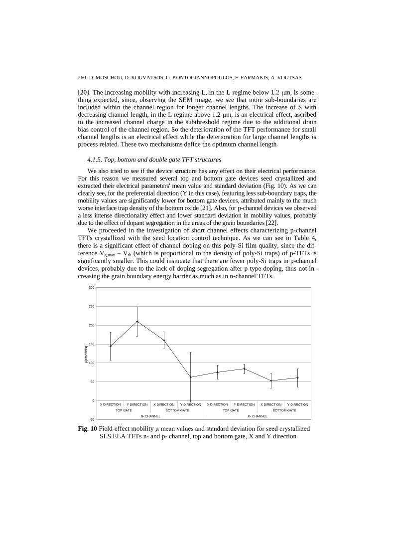
We also tried to see if the device structure has any effect on their electrical performance. For this reason we measured several top and bottom gate devices seed crystallized and extracted their electrical parameters' mean value and standard deviation (Fig. 10). As we can clearly see, for the preferential direction (Y in this case), featuring less sub-boundary traps, the mobility values are significantly lower for bottom gate devices, attributed mainly to the much worse interface trap density of the bottom oxide [21]. Also, for p-channel devices we observed a less intense directionality effect and lower standard deviation in mobility values, probably due to the effect of dopant segregation in the areas of the grain boundaries [22].
We proceeded in the investigation of short channel effects characterizing p-channel
TFTs crystallized with the seed location control technique. As we can see in Table 4,
there is a significant effect of channel doping on this poly-Si film quality, since the dif-
ference Vg,max – Vth (which is proportional to the density of poly-Si traps) of p-TFTs is
significantly smaller. This could insinuate that there are fewer poly-Si traps in p-channel
devices, probably due to the lack of doping segregation after p-type doping, thus not in-
creasing the grain boundary energy barrier as much as in n-channel TFTs.
Fig. 10 Field-effect mobility μ mean values and standard deviation for seed crystallized
SLS ELA TFTs n- and p- channel, top and bottom gate, X and Y direction
-50
0
50
100
150
200
250
300
X DIRECTION Υ DIRECTION Χ DIRECTION Υ DIRECTION X DIRECTION Υ DIRECTION Χ DIRECTION Υ DIRECTION
TOP GATE BOTTOM GATE TOP GATE BOTTOM GATE
Ν- CHANNEL Ρ- CHANNEL
μ(c
m^
2/V
s)

Technology, Performance and Degradation Characteristics of SLS ELA Thin Film Transistors 261
Table 4 Mean electrical parameter values for seed location control technique
n- and p- channel TFTs
Vth (V) μ (cm2/V·sec) S (V/decade) Vg,max – Vth (V)
Direction n- p- n- p- n- p- n- p-
Χ 0,78 -0,99 144,51 75,38 0,14 0,12 1,59 0,85 Υ 0,35 -0,86 209,85 84,30 0,13 0,12 1,17 0,85
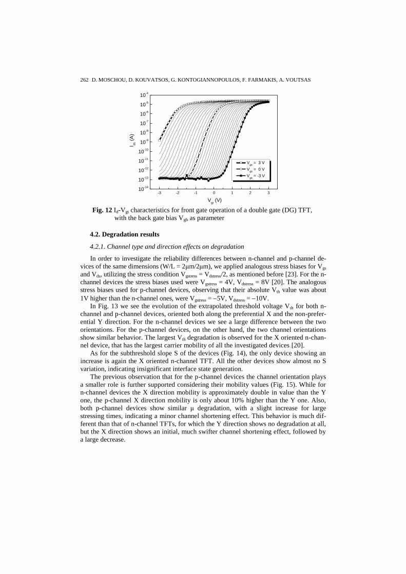
Following that, we characterized double gate devices with a structure schematically shown in Fig. 11, fabricated with the same process as the single gate devices previously analysed. While varying their bottom gate bias as a parameter, we recorded their transfer characteristics Id – Vgt for top gate operation, as shown in Fig. 12. It is evident that there is a continuous shift of the Id – Vgt characteristic for changing Vgb value, indicating a continuous back gate effect and strongly suggesting that the device is fully depleted at all conditions. The device parameters (Vth, S, Gm,max), as measured for front gate operation, were observed to depend on Vgb in a manner reflecting the varying back channel contribution, with a confluence of Vth and S values for varying Vgb. However, the use of the back gate was determined to offer linear threshold voltage control, thus allowing for enhanced flexibility in TFT circuit design. Moreover, the application of back gate bias makes possible the significant reduction, for similar drain current levels, of the avalanche effect observed at high drain voltage values, as compared to the case when only a front gate bias is applied [15].
Fig. 11 Schematic of double gate TFT structure
BOTTOM GATE poly-Si N+
TOP GATE
DIELECTRIC SiO2
(30nm)
TOP GATE poly-Si
N+
SOURCE N+ DRAIN N+ELA poly-Si 50nm
(ACTIVE LAYER)
BOTTOM GATE DIELECTRIC
SiO2 (50nm)
Ltop
Lbottom
CHANNEL
262 D. MOSCHOU, D. KOUVATSOS, G. KONTOGIANNOPOULOS, F. FARMAKIS, A. VOUTSAS
Fig. 12 Id-Vgt characteristics for front gate operation of a double gate (DG) TFT,
with the back gate bias Vgb as parameter
4.2. Degradation results
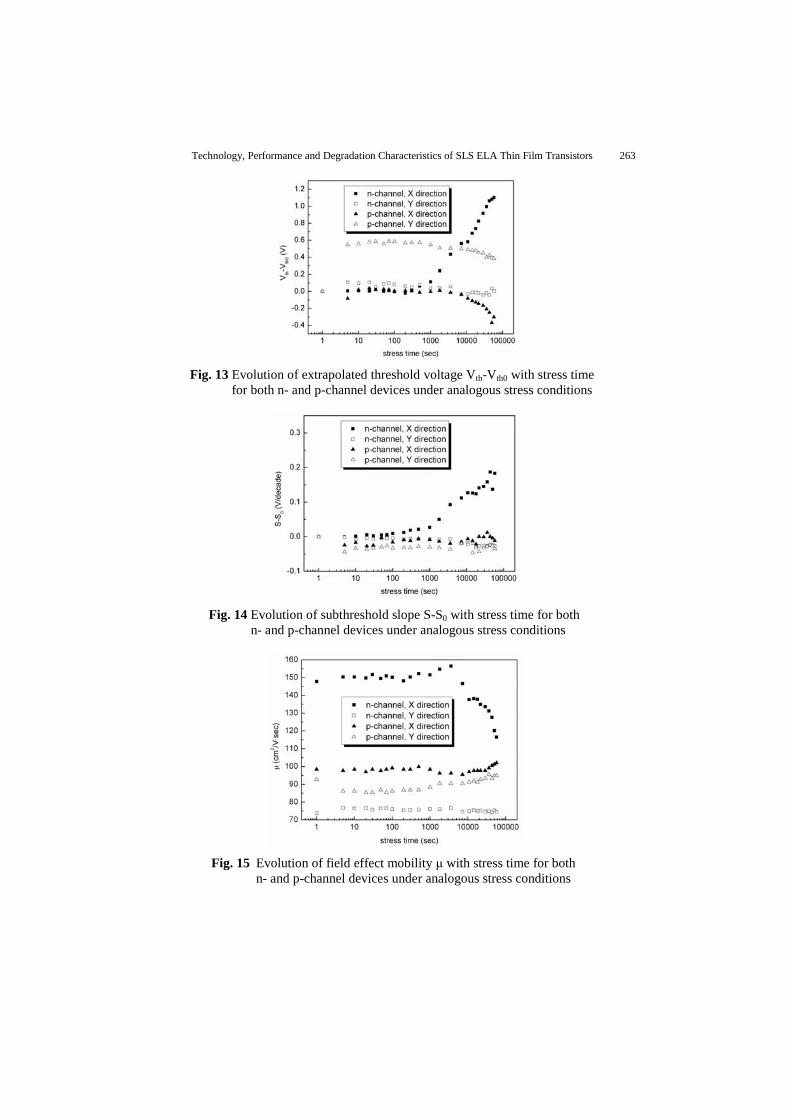
4.2.1. Channel type and direction effects on degradation
In order to investigate the reliability differences between n-channel and p-channel de-
vices of the same dimensions (W/L = 2μm/2μm), we applied analogous stress biases for Vgs
and Vds, utilizing the stress condition Vgstress = Vdstress/2, as mentioned before [23]. For the n-
channel devices the stress biases used were Vgstress = 4V, Vdstress = 8V [20]. The analogous
stress biases used for p-channel devices, observing that their absolute Vth value was about
1V higher than the n-channel ones, were Vgstress = 5V, Vdstress = 10V.
In Fig. 13 we see the evolution of the extrapolated threshold voltage Vth for both n-
channel and p-channel devices, oriented both along the preferential X and the non-prefer-
ential Y direction. For the n-channel devices we see a large difference between the two
orientations. For the p-channel devices, on the other hand, the two channel orientations
show similar behavior. The largest Vth degradation is observed for the X oriented n-chan-
nel device, that has the largest carrier mobility of all the investigated devices [20].
As for the subthreshold slope S of the devices (Fig. 14), the only device showing an
increase is again the X oriented n-channel TFT. All the other devices show almost no S
variation, indicating insignificant interface state generation.
The previous observation that for the p-channel devices the channel orientation plays
a smaller role is further supported considering their mobility values (Fig. 15). While for
n-channel devices the X direction mobility is approximately double in value than the Y
one, the p-channel X direction mobility is only about 10% higher than the Y one. Also,
both p-channel devices show similar μ degradation, with a slight increase for large
stressing times, indicating a minor channel shortening effect. This behavior is much dif-
ferent than that of n-channel TFTs, for which the Y direction shows no degradation at all,
but the X direction shows an initial, much swifter channel shortening effect, followed by
a large decrease.
-3 -2 -1 0 1 2 310
-14
10-13
10-12
10-11
10-10
10-9
10-8
10-7
10-6
10-5
10-4
Vgb
= 3 V
Vgb
= 0 V
Vgb
= -3 V
I ds (
A)
Vgt (V)
Technology, Performance and Degradation Characteristics of SLS ELA Thin Film Transistors 263
Fig. 13 Evolution of extrapolated threshold voltage Vth-Vth0 with stress time
for both n- and p-channel devices under analogous stress conditions
Fig. 14 Evolution of subthreshold slope S-S0 with stress time for both
n- and p-channel devices under analogous stress conditions
Fig. 15 Evolution of field effect mobility μ with stress time for both
n- and p-channel devices under analogous stress conditions
264 D. MOSCHOU, D. KOUVATSOS, G. KONTOGIANNOPOULOS, F. FARMAKIS, A. VOUTSAS
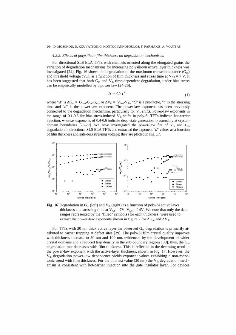
4.2.2. Effects of polysilicon film thickness on degradation mechanisms
For directional SLS ELA TFTs with channels oriented along the elongated grains the
variation of degradation mechanisms for increasing polysilicon active layer thickness was
investigated [24]. Fig. 16 shows the degradation of the maximum transconductance (Gm)
and threshold voltage (Vth), as a function of film thickness and stress time at VGS = 7 V. It
has been suggested that both Gm and Vth time-dependent degradation, under bias stress
can be empirically modelled by a power law [24-26]:
ntC (1)
where "" is Gm = |Gm,o-Gm|/Gm,o or Vth = |Vth,o-Vth|, "C" is a pre-factor, "t" is the stressing
time and "n" is the power-law exponent. The power-law exponent has been previously
connected to the degradation mechanism, particularly for Vth shifts. Power-law exponents in
the range of 0.1-0.3 for bias-stress-induced Vth shifts in poly-Si TFTs indicate hot-carrier
injection, whereas exponents of 0.4-0.6 indicate deep-state generation, presumably at crystal-
domain boundaries [26-29]. We have investigated the power-law fits of Vth and Gm
degradation in directional SLS ELA TFTs and extracted the exponent "n" values as a function
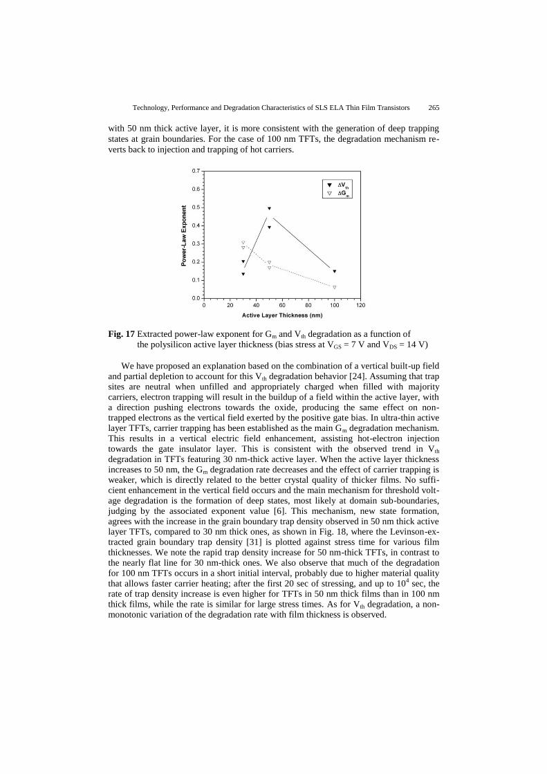
of film thickness and gate-bias stressing voltage; they are plotted in Fig. 17.
Fig. 16`Degradation in Gm (left) and Vth (right) as a function of poly-Si active layer
thickness and stressing time at VGS = 7V, VDS = 14V. We note that only the data
ranges represented by the "filled" symbols (for each thickness) were used to
extract the power-law exponents shown in figure 2 for Gm and Vth
For TFTs with 30 nm thick active layer the observed Gm degradation is primarily at-
tributed to carrier trapping at defect sites [29]. The poly-Si film crystal quality improves
with thickness increase to 50 nm and 100 nm, evidenced by the development of wider
crystal domains and a reduced trap density in the sub-boundary regions [30]; thus, the Gm
degradation rate decreases with film thickness. This is reflected in the declining trend in
the power-law exponent with the active-layer thickness, shown in Fig. 17. However, the
Vth degradation power-law dependence yields exponent values exhibiting a non-mono-
tonic trend with film thickness. For the thinnest value (30 nm) the Vth degradation mech-
anism is consistent with hot-carrier injection into the gate insulator layer. For devices
Technology, Performance and Degradation Characteristics of SLS ELA Thin Film Transistors 265
with 50 nm thick active layer, it is more consistent with the generation of deep trapping
states at grain boundaries. For the case of 100 nm TFTs, the degradation mechanism re-
verts back to injection and trapping of hot carriers.
Fig. 17 Extracted power-law exponent for Gm and Vth degradation as a function of
the polysilicon active layer thickness (bias stress at VGS = 7 V and VDS = 14 V)
We have proposed an explanation based on the combination of a vertical built-up field and partial depletion to account for this Vth degradation behavior [24]. Assuming that trap sites are neutral when unfilled and appropriately charged when filled with majority carriers, electron trapping will result in the buildup of a field within the active layer, with a direction pushing electrons towards the oxide, producing the same effect on non-trapped electrons as the vertical field exerted by the positive gate bias. In ultra-thin active layer TFTs, carrier trapping has been established as the main Gm degradation mechanism. This results in a vertical electric field enhancement, assisting hot-electron injection towards the gate insulator layer. This is consistent with the observed trend in Vth degradation in TFTs featuring 30 nm-thick active layer. When the active layer thickness increases to 50 nm, the Gm degradation rate decreases and the effect of carrier trapping is weaker, which is directly related to the better crystal quality of thicker films. No suffi-cient enhancement in the vertical field occurs and the main mechanism for threshold volt-age degradation is the formation of deep states, most likely at domain sub-boundaries, judging by the associated exponent value [6]. This mechanism, new state formation, agrees with the increase in the grain boundary trap density observed in 50 nm thick active layer TFTs, compared to 30 nm thick ones, as shown in Fig. 18, where the Levinson-ex-tracted grain boundary trap density [31] is plotted against stress time for various film thicknesses. We note the rapid trap density increase for 50 nm-thick TFTs, in contrast to the nearly flat line for 30 nm-thick ones. We also observe that much of the degradation for 100 nm TFTs occurs in a short initial interval, probably due to higher material quality that allows faster carrier heating; after the first 20 sec of stressing, and up to 10
4 sec, the
rate of trap density increase is even higher for TFTs in 50 nm thick films than in 100 nm thick films, while the rate is similar for large stress times. As for Vth degradation, a non-monotonic variation of the degradation rate with film thickness is observed.

266 D. MOSCHOU, D. KOUVATSOS, G. KONTOGIANNOPOULOS, F. FARMAKIS, A. VOUTSAS
Fig. 18 Grain boundary trap density Nt evolution with stress time,
for various active layer thicknesses. Nt,o is the value of Nt at t = 0 sec
For TFTs in the thicker 100 nm films the buildup of a negative field within the active layer is even less pronounced than for the 50 nm case. However, hot electron injection and trapping is again inferred, from the power law exponent, as for the 30 nm devices, to be the dominant degradation mechanism; the higher extracted exponent value, indicating a domi-nant mechanism of generation of deep trapping states at grain boundaries, is only observed in the 50 nm case. This is explained using the reasonable assumption that the 100 nm thick poly-Si film is only partially depleted, while the 30 nm and 50 nm thick ones are fully de-pleted. Actually, in SOI device studies a film thickness of 100 nm has been identified as the boundary between full depletion and partial depletion regimes [32]. As the defect density in polysilicon is higher than in single crystal SOI films, we expect this demarcation point to be shifted towards thinner active layer thickness. Thus, even though the bulk field due to filled traps, which enhances hot electron injection, for 100 nm thick TFTs is even lower than 50 nm ones, in the 100nm case many active layer electrons recombine in the neutral region at the bottom of the film and do not contribute to new sub-boundary state creation. That is, the partial depletion suppresses that mechanism for the thickest films.
4.2.3. Channel width effects on degradation
Since channel dimensions are a critical parameter for high-performance devices, we tried to clarify the degradation mechanisms observed by varying the channel width. A DC hot-carrier stress (VGS,stress, VDS,stress) = (3 V, 6 V) was applied for durations up to 60 h; the IDS – VGS curves were recorded at the conclusion of each stress cycle and the device parameters were extracted. In order to investigate the channel width dependence of stress-induced effects in polysilicon TFTs, we applied that same electrical stress condition in devices with various gate widths from 4 to 100 μm.
Fig. 19 shows the deviation of the initial threshold voltage ΔVth, extracted after each stress cycle for devices with different channel widths. We observe an increase of ΔVth during stress time, which is a common behavior in all devices except for the narrower devices that exhibit an initial decrease and then an increase. The amplitude of positive ΔVth shift scales up with width. Narrower devices (with W of 4 and 8 μm) demonstrate less

Technology, Performance and Degradation Characteristics of SLS ELA Thin Film Transistors 267
pronounced ΔVth positive shift. Moreover, the onset of positive Vth shift occurs at shorter stress durations for wider devices than for narrower ones and it starts progressively earlier with increasing width. We also witness two slopes in the ΔVth vs. logarithmic stress duration plot for all devices except for the narrower ones. Beyond a transition point, which scales down with width, the ΔVth vs. logarithmic stress duration curve exhibits a second slope, which seems to be width-independent and is of the same magnitude for all devices. On the contrary, the magnitude of the slope of each curve up to the above mentioned transition point, depends on width and is progressively larger for the wider devices [33].
100
101
102
103
104
105
106
-0.2
-0.1
0.0
0.1
0.2
0.3
0.4
0.5
0.6
0.7
0.8
0.9
1.0
1.1
1.2 Stress condition:
VGS,stress
=3 V, VDS,stress
=6 V
W = 4 ìm
W = 8 ìm
W = 16 ìm
W = 32 ìm
W = 100 ìm
ÄV
th [
V]
Time [s]
X direction
Fig. 19 Threshold voltage variation during stress for X-directed polysilicon TFTs
with various channel widths
100
101
102
103
104
105
-80
-70
-60
-50
-40
-30
-20
-10
0
10
20
30Stress condition:
VGS,stress
=3 V, VDS,stress
=6 V
X direction
W = 4 μm
W = 8 μm
W = 16 μm
W = 32 μm
W = 100 μm
-(G
m,m
ax-G
m,0)/
Gm
,0 (%
)
Time [s]
Fig. 20 Percentage change of transconductance maximum
vs. stress time for X-directed polysilicon TFTs
Fig. 20 shows the percentage change of the maximum of transconductance vs. stress
time for X-directed TFTs. We observe that the devices with W = 16, 32 and 100 μm ex-
hibit a similar behavior, which is an initial increase in Gm,max (transconductance "over-
268 D. MOSCHOU, D. KOUVATSOS, G. KONTOGIANNOPOULOS, F. FARMAKIS, A. VOUTSAS
shoot") and then a reduction after reaching a maximum Gm,max value. In the case of nar-
row devices (W = 4 and 8 μm), Gm,max continuously decreases during stress and no "over-
shoot" is observed. Again, the initial increase of transconductance for wider devices
scales up with width, whereas the later decrease is common and of the same magnitude
for all the devices, independently of width. It is worth noticing that the transition point of
stress duration, after which Gm,max demonstrates a reduction from the maximum value,
corresponds to the same transition point where the second slope in ΔVth vs. log(t) curve
(Fig. 19) appears for devices with W = 32 and 100 μm. We have to mention that for the
narrowest device (W = 4 μm) only one slope in the ΔVth vs. log(t) curve (Fig. 19) is de-
tected and for the device with W = 8 μm the two slopes are slightly distinguished.
The difference in stress induced degradation behavior between narrow and wider de-
vices reflects the fact that in the latter case the drain current is much larger, with less pro-
nounced edge effects, and the electrons carrying it acquire larger energy, as self-heating
effects are more pronounced; this increases the probability of hot electron injection. In
the case of narrow TFTs this source of energy is not significant and hot holes are mainly
responsible for the degradation, since they have larger effective mass and induce interface
state generation, as inferred from the severe Gm,max degradation [33].
4.2.4. Short channel effects on LTPS TFT degradation
The scope of our work in this field was to determine if there are any short channel
effects present in the degradation of SLS ELA TFTs [34]. The investigated TFTs were n-
channel double gate devices [15] with 50 nm polysilicon films that were formed by ex-
cimer-laser annealing of amorphous silicon, using the single-shot location control varia-
tion of the sequential lateral solidification (SLS) technique, preferentially oriented. The
DG TFTs were dc stressed using a HP4140B semiconductor analyzer and a Keithley 230
voltage source. The transfer characteristics Ids − Vgt with respect to the top gate bias Vgt
for a back gate bias Vgb = −3 V, so as to ensure the conduction is mainly at the top inter-
face, were measured in the linear region with Vd = 0.1 V after each stress cycle. To ex-
clude effects from horizontal field variation, due to the different channel length, Vdstress
was scaled proportionally to Ltop for each device. The top gate stress bias was selected to
be Vgtstress = Vth(Vgb = −3 V) + 2 V, while the bottom gate bias Vgbstress was kept constant
at -3 V, as stated before, pushing the carriers to the top interface.
We applied dc stress to double gate TFTs with different top gate length Ltop, channel width of W = 8 μm and bottom gate length Lbottom = 4 μm. Observing the current-voltage characteristic curves after each stress cycle (Figs. 21-23) we saw that the degradation becomes much more intense for longer channels, although the horizontal electric field is exactly the same as for the shorter ones. We believe that this is attributed to the structure of the polysilicon film, since the longer the channel the more grain boundaries and sub-boundaries will be present. The more traps are present within the film the larger the deg-radation that will occur in the device, due to the extra trap state generation in these loca-tions. We also observed two Vth degradation mechanisms: hole injection observed only for large channels and electron injection common for all devices. From S evolution with dc stress we saw that these mechanisms mainly refer to trap generation at the interface and not oxide injection. As for Gm,max, we saw a similar behavior for all TFTs, featuring a monotonous decrease. This was attributed to grain boundary and sub-boundary trap gen-eration, as indicated also by the Vg,max − Vth evolution with stress time. The proposed degradation mechanisms are supported by low frequency noise measurements.

Technology, Performance and Degradation Characteristics of SLS ELA Thin Film Transistors 269
Fig. 21 Id-Vgt curves after successive dc stress cycles for a DG TFT with Ltop = 0.5 μm
Fig. 22 Id-Vgt curves after successive dc stress cycles for a DG TFT with Ltop = 0.8 μm
Fig. 23 Id-Vgt curves after successive dc stress cycles for a DG TFT with Ltop = 1.3 μm
-3 -2 -1 0 1 2 3 4 5-14
-13
-12
-11
-10
-9
-8
-7
-6
-5
-4
Stress duration (s)
0
10
100
1000
10800
18000
log
I ds (
A)
Vgt (V)
-3 -2 -1 0 1 2 3 4 5-14
-13
-12
-11
-10
-9
-8
-7
-6
-5
-4
Stress duration (s)
0
10
100
1000
10800
18000
log
I ds (
A)
Vgt (V)
-3 -2 -1 0 1 2 3 4 5-14
-13
-12
-11
-10
-9
-8
-7
-6
-5
-4
Stress duration (s)
0
10
100
1000
10800
18000
logI d
s (
A)
Vgt (V)

270 D. MOSCHOU, D. KOUVATSOS, G. KONTOGIANNOPOULOS, F. FARMAKIS, A. VOUTSAS
4.2.5. Degradation modeling
One of the major issues associated with the high performance of polysilicon TFTs is their
reliability when they are subjected to a high drain bias and a variety of gate bias voltages [26,
35, 36]. Due to the enhanced fields, mainly near the drain junction, the performance of TFTs
is degraded, and their electrical parameters are shifted, leading to unpredictable circuit design
failures when TFTs are used as circuit elements [37]. Our motivation for the following studies
was to provide a simple and practical model that predicts the shift of the electrical parameters
of polysilicon TFTs subjected to high stressing fields, both as a function of the stress regime
(condition) and with regard to the scalability of the channel width. The width is an essential
parameter for circuit designers, as in tapered (scaled) inverter chain complementary MOS
circuits implemented using consecutive (cascade) inverter stages with W/L transistor ratios
many times larger than those for previous stages [37]. Moreover, the operation conditions of
TFTs used as circuit elements (as in cascode configurations [38]) are different for each device,
resulting in electrical parameter shifts (compared to linear operation) and circuit design pitfalls
that must be predicted and related to stress damage.
Even though hot-carrier phenomena have widely been studied in MOS poly-TFT
structures [39], their quantitative [40] impact in the reliability and performance
characteristics of poly-TFT devices of different channel widths after electrical stressing
under different stressing conditions has been described only to a limited extent. Moreo-
ver, even in the models developed for the mature technology of silicon-on-insulator devices
[41], typical bulk MOSFETs [42], and a-Si:H TFTs [43], the effect of subjecting devices
with various channel widths under different hot-carrier stress conditions has not been
analyzed, and mainly shallow trench isolation p-type MOS devices were examined [44].
Consequently, the effect of different hot-carrier stressing conditions on the 1-D current–
voltage characteristics as a function of the channel width needed to be further examined.
The developed degradation model takes into account the formation of two regions,
i.e., a defective region and a non-defective one, as presented elsewhere [42]. The equiva-
lent circuit model [45] of a device subjected to the electrical stress is represented by two
TFTs connected in series (Fig. 24).
Stressed Device
RS/2
W/(L-ΔL) W/ΔL
Series
Resistance
(source)
Transistor with non
Defective Channel
Region
Transistor with
Defective Channel
Region
RS/2
Series
Resistance
(drain)
Fig. 24 Schematic of TFT structure (left) and its equivalent electrical representation after
electrical stressing (right). The developed model suggests the formation of two
channel regions that are represented by two transistors connected in series
In order to obtain a simple and practical expression, so as to predict the hot-carrier damage
for large-grain-size polysilicon TFTs, we use the ON-current model proposed in [46], i.e.,
1
( )1 ( / )( / )exp( / ) 1 ( )
GD ox G th D
G GB GB G b G th
WI C V V V
L L L qV kT V V
(2)
Technology, Performance and Degradation Characteristics of SLS ELA Thin Film Transistors 271
where LGB is the average grain boundary length, LG is the average intragrain length, μG is the intragrain mobility, and μGB is the grain boundary mobility. From (1), the effective mobility is given by
0
11 ( )( )exp( ) 1 ( )
Geff
G GB GB G b G thL L qV kT V V
1 ( )( )exp( ) 1 ( )G GB GB G b G thG GB GB G b G thG GB GB G b G thG GB GB G b G th1 ( )( )exp( ) 1 ( )G GB GB G b G th1 ( )( )exp( ) 1 ( )L L qV kT V V1 ( )( )exp( ) 1 ( )G GB GB G b G th1 ( )( )exp( ) 1 ( )
1 ( )( )exp( ) 1 ( ) 1 ( )( )exp( ) 1 ( )1 ( )( )exp( ) 1 ( ) 1 ( )( )exp( ) 1 ( )1 ( )( )exp( ) 1 ( )L L qV kT V V1 ( )( )exp( ) 1 ( ) 1 ( )( )exp( ) 1 ( )L L qV kT V V1 ( )( )exp( ) 1 ( )1 ( )( )exp( ) 1 ( )L L qV kT V V1 ( )( )exp( ) 1 ( ) 1 ( )( )exp( ) 1 ( )L L qV kT V V1 ( )( )exp( ) 1 ( )1 ( )( )exp( ) 1 ( )L L qV kT V V1 ( )( )exp( ) 1 ( ) 1 ( )( )exp( ) 1 ( )L L qV kT V V1 ( )( )exp( ) 1 ( ) 1 ( )( )exp( ) 1 ( ) 1 ( )( )exp( ) 1 ( )G GB GB G b G th G GB GB G b G thG GB GB G b G th G GB GB G b G thG GB GB G b G th G GB GB G b G thG GB GB G b G th G GB GB G b G th1 ( )( )exp( ) 1 ( )G GB GB G b G th1 ( )( )exp( ) 1 ( ) 1 ( )( )exp( ) 1 ( )G GB GB G b G th1 ( )( )exp( ) 1 ( )1 ( )( )exp( ) 1 ( )G GB GB G b G th1 ( )( )exp( ) 1 ( ) 1 ( )( )exp( ) 1 ( )G GB GB G b G th1 ( )( )exp( ) 1 ( )1 ( )( )exp( ) 1 ( )G GB GB G b G th1 ( )( )exp( ) 1 ( )L L qV kT V V1 ( )( )exp( ) 1 ( )G GB GB G b G th1 ( )( )exp( ) 1 ( ) 1 ( )( )exp( ) 1 ( )G GB GB G b G th1 ( )( )exp( ) 1 ( )L L qV kT V V1 ( )( )exp( ) 1 ( )G GB GB G b G th1 ( )( )exp( ) 1 ( )1 ( )( )exp( ) 1 ( )G GB GB G b G th1 ( )( )exp( ) 1 ( )L L qV kT V V1 ( )( )exp( ) 1 ( )G GB GB G b G th1 ( )( )exp( ) 1 ( ) 1 ( )( )exp( ) 1 ( )G GB GB G b G th1 ( )( )exp( ) 1 ( )L L qV kT V V1 ( )( )exp( ) 1 ( )G GB GB G b G th1 ( )( )exp( ) 1 ( )1 ( )( )exp( ) 1 ( )G GB GB G b G th1 ( )( )exp( ) 1 ( )L L qV kT V V1 ( )( )exp( ) 1 ( )G GB GB G b G th1 ( )( )exp( ) 1 ( ) 1 ( )( )exp( ) 1 ( )G GB GB G b G th1 ( )( )exp( ) 1 ( )L L qV kT V V1 ( )( )exp( ) 1 ( )G GB GB G b G th1 ( )( )exp( ) 1 ( )1 ( )( )exp( ) 1 ( )G GB GB G b G th1 ( )( )exp( ) 1 ( )L L qV kT V V1 ( )( )exp( ) 1 ( )G GB GB G b G th1 ( )( )exp( ) 1 ( ) 1 ( )( )exp( ) 1 ( )G GB GB G b G th1 ( )( )exp( ) 1 ( )L L qV kT V V1 ( )( )exp( ) 1 ( )G GB GB G b G th1 ( )( )exp( ) 1 ( )1 ( )( )exp( ) 1 ( ) 1 ( )( )exp( ) 1 ( )1 ( )( )exp( ) 1 ( ) 1 ( )( )exp( ) 1 ( ) 1 ( )( )exp( ) 1 ( ) 1 ( )( )exp( ) 1 ( )1 ( )( )exp( ) 1 ( ) 1 ( )( )exp( ) 1 ( ) 1 ( )( )exp( ) 1 ( ) 1 ( )( )exp( ) 1 ( )1 ( )( )exp( ) 1 ( )G GB GB G b G th1 ( )( )exp( ) 1 ( ) 1 ( )( )exp( ) 1 ( )G GB GB G b G th1 ( )( )exp( ) 1 ( ) 1 ( )( )exp( ) 1 ( )G GB GB G b G th1 ( )( )exp( ) 1 ( ) 1 ( )( )exp( ) 1 ( )G GB GB G b G th1 ( )( )exp( ) 1 ( )1 ( )( )exp( ) 1 ( )G GB GB G b G th1 ( )( )exp( ) 1 ( ) 1 ( )( )exp( ) 1 ( )G GB GB G b G th1 ( )( )exp( ) 1 ( ) 1 ( )( )exp( ) 1 ( )G GB GB G b G th1 ( )( )exp( ) 1 ( ) 1 ( )( )exp( ) 1 ( )G GB GB G b G th1 ( )( )exp( ) 1 ( )1 ( )( )exp( ) 1 ( )L L qV kT V V1 ( )( )exp( ) 1 ( ) 1 ( )( )exp( ) 1 ( )L L qV kT V V1 ( )( )exp( ) 1 ( ) 1 ( )( )exp( ) 1 ( )L L qV kT V V1 ( )( )exp( ) 1 ( ) 1 ( )( )exp( ) 1 ( )L L qV kT V V1 ( )( )exp( ) 1 ( )1 ( )( )exp( ) 1 ( )L L qV kT V V1 ( )( )exp( ) 1 ( ) 1 ( )( )exp( ) 1 ( )L L qV kT V V1 ( )( )exp( ) 1 ( ) 1 ( )( )exp( ) 1 ( )L L qV kT V V1 ( )( )exp( ) 1 ( ) 1 ( )( )exp( ) 1 ( )L L qV kT V V1 ( )( )exp( ) 1 ( )1 ( )( )exp( ) 1 ( )L L qV kT V V1 ( )( )exp( ) 1 ( ) 1 ( )( )exp( ) 1 ( )L L qV kT V V1 ( )( )exp( ) 1 ( ) 1 ( )( )exp( ) 1 ( )L L qV kT V V1 ( )( )exp( ) 1 ( ) 1 ( )( )exp( ) 1 ( )L L qV kT V V1 ( )( )exp( ) 1 ( )1 ( )( )exp( ) 1 ( )G GB GB G b G th1 ( )( )exp( ) 1 ( )L L qV kT V V1 ( )( )exp( ) 1 ( )G GB GB G b G th1 ( )( )exp( ) 1 ( ) 1 ( )( )exp( ) 1 ( )G GB GB G b G th1 ( )( )exp( ) 1 ( )L L qV kT V V1 ( )( )exp( ) 1 ( )G GB GB G b G th1 ( )( )exp( ) 1 ( ) 1 ( )( )exp( ) 1 ( )G GB GB G b G th1 ( )( )exp( ) 1 ( )L L qV kT V V1 ( )( )exp( ) 1 ( )G GB GB G b G th1 ( )( )exp( ) 1 ( ) 1 ( )( )exp( ) 1 ( )G GB GB G b G th1 ( )( )exp( ) 1 ( )L L qV kT V V1 ( )( )exp( ) 1 ( )G GB GB G b G th1 ( )( )exp( ) 1 ( )1 ( )( )exp( ) 1 ( )G GB GB G b G th1 ( )( )exp( ) 1 ( )L L qV kT V V1 ( )( )exp( ) 1 ( )G GB GB G b G th1 ( )( )exp( ) 1 ( ) 1 ( )( )exp( ) 1 ( )G GB GB G b G th1 ( )( )exp( ) 1 ( )L L qV kT V V1 ( )( )exp( ) 1 ( )G GB GB G b G th1 ( )( )exp( ) 1 ( ) 1 ( )( )exp( ) 1 ( )G GB GB G b G th1 ( )( )exp( ) 1 ( )L L qV kT V V1 ( )( )exp( ) 1 ( )G GB GB G b G th1 ( )( )exp( ) 1 ( ) 1 ( )( )exp( ) 1 ( )G GB GB G b G th1 ( )( )exp( ) 1 ( )L L qV kT V V1 ( )( )exp( ) 1 ( )G GB GB G b G th1 ( )( )exp( ) 1 ( )1 ( )( )exp( ) 1 ( )G GB GB G b G th1 ( )( )exp( ) 1 ( )L L qV kT V V1 ( )( )exp( ) 1 ( )G GB GB G b G th1 ( )( )exp( ) 1 ( ) 1 ( )( )exp( ) 1 ( )G GB GB G b G th1 ( )( )exp( ) 1 ( )L L qV kT V V1 ( )( )exp( ) 1 ( )G GB GB G b G th1 ( )( )exp( ) 1 ( ) 1 ( )( )exp( ) 1 ( )G GB GB G b G th1 ( )( )exp( ) 1 ( )L L qV kT V V1 ( )( )exp( ) 1 ( )G GB GB G b G th1 ( )( )exp( ) 1 ( ) 1 ( )( )exp( ) 1 ( )G GB GB G b G th1 ( )( )exp( ) 1 ( )L L qV kT V V1 ( )( )exp( ) 1 ( )G GB GB G b G th1 ( )( )exp( ) 1 ( )(3)
The first term of the effective mobility expresses the effect of the grains and grain
boundaries of polysilicon TFTs for low gate fields (low field mobility, denoted as μo in the text), and the second term expresses the first-order surface scattering effect on the mobility attenuation [47].
Assuming monoenergetic traps at the grain boundaries, the grain boundary potential barrier is gate voltage modulated and is given by the relation
2( )8 ( )
si tGBb
si ox G th
t qNVC V V
(4)
After theoretical calculations, utilizing the above mentioned assumptions [45] we ob-tain the model fitting function, i.e.,
2 2 2 20, 0, 0 ,, ,( ) ( ) ( )
m DS ox
DS nd GS th nd GS th d GS thnd nd d
g V C L L LI W V V W V V W V V
(5)
In the latter equation 4, the terms of the left-hand side are all determined by the measured data. The right-hand side is the fitting function that contains all the previously reported fitting parameters. By fitting the derived equation of the model to the experimental data, which correspond to the region VGS > VGS,peak, we obtained the parameters of the presented model. It should be noted that the parameters obtained from the fitting take their mean values.
We suggest that the degradation model predicts the maximum value of the threshold voltage of the two devices, corresponding to the two regions (defective and non-defec-tive), connected in series in the equivalent circuit, which is expected to be the combined Vth for two devices in series. If the degradation is uniform, the corresponding threshold voltage will be equal for the two regions, whereas if the damage is non-uniform (but more or less extended along the channel) the predicted threshold voltage of the whole device is, to a good approximation, that of the one at the defective channel region (which is the larger one). This approximation is supported theoretically [48]; in a non-uniform channel, with regions having different local threshold voltages each of which is considered as a separate device, the overall Vth is the weighted Vth over the channel (i.e., that of each device). However, as inversion in the defective channel part is harder to achieve, reflecting a much larger weight, the overall weighted threshold voltage is the average threshold voltage of the defective channel part. This is reasonable, as the threshold voltage reflects the mean concentration of free carriers and not how these carriers are transported between the source and the drain. The damage that occurs in the defective part of the channel region is reflected in two additional parameters: the defective region length ΔL, which is proportional to the interface state and/or the oxide trap state creation, and the mobility of charge carriers in the defective channel portion that depends on the defect charge density at the Si/SiO2 interface and/or in the oxide.
Fig. 25 demonstrates the extracted threshold voltage shift (dot lines) and the overall threshold voltage shift predicted by the model (solid lines) for devices with different
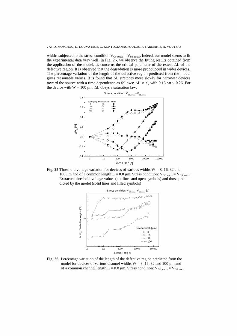
272 D. MOSCHOU, D. KOUVATSOS, G. KONTOGIANNOPOULOS, F. FARMAKIS, A. VOUTSAS
widths subjected to the stress condition VGS,stress = VDS,stress. Indeed, our model seems to fit the experimental data very well. In Fig. 26, we observe the fitting results obtained from the application of the model, as concerns the critical parameter of the extent ΔL of the defective region. It is observed that the degradation is more pronounced in wider devices. The percentage variation of the length of the defective region predicted from the model gives reasonable values. It is found that ΔL stretches more slowly for narrower devices
toward the source with a time dependence as follows: ΔL tn, with 0.16 n 0.26. For
the device with W = 100 μm, ΔL obeys a saturation law.
1 10 100 1000 10000 100000-0.4
-0.2
0.0
0.2
0.4
0.6
0.8
Stress condition: VGS,stress
=VDS,stress
ΔV
th [V
]
Stress time [s]
Width [μm] Measurement Model
8
16
32
100
Fig. 25 Threshold voltage variation for devices of various widths W = 8, 16, 32 and
100 μm and of a common length L = 0.8 μm. Stress condition: VGS,stress = VDS,stress.
Extracted threshold voltage values (dot lines and open symbols) and those pre-
dicted by the model (solid lines and filled symbols)
10 100 1000 10000 1000001
10
Device width [μm]:
Stress condition: VGS,stress
=VDS,stress
[V]
ΔL
/L0, D
ed
ective
re
gio
n (
%)
Stress Time [s]
8
16
32
100
Fig. 26 Percentage variation of the length of the defective region predicted from the
model for devices of various channel widths W = 8, 16, 32 and 100 μm and
of a common channel length L = 0.8 μm. Stress condition: VGS,stress = VDS,stress

Technology, Performance and Degradation Characteristics of SLS ELA Thin Film Transistors 273
4.2.6. Double gate TFT degradation mechanisms
However, attaining high performance is not enough, as one of the major issues associ-
ated with polysilicon TFTs is their reliability. The application of bias stress with high
drain and gate voltages degrades the performance of TFTs due to hot carrier effects
caused mainly by the enhanced field near the drain junction [49]. Even though hot carrier
phenomena are widely studied [26, 36, 39], it is not clear yet whether degradation
phenomena may also occur at the back interface between the polysilicon film and silicon
dioxide, at least for fully depleted TFTs as is the case of fully depleted SOI MOSFETs
[50]. The scope of this work [51] is to provide evidences for degradation mechanisms at
this back interface of the device, via the aid of fully depleted double-gate (DG) polysili-
con TFTs. The investigated TFTs were n-channel double-gate devices. The polysilicon
films were formed by excimer laser annealing of amorphous silicon, using the "single-
shot" variation of the SLS technique. DC hot carrier stress conditions (VGF,stress, VDS,stress,
VGB,stress) were applied for durations up to 27,000 s, the IDS – VGF curves were recorded at
the end of each stress cycle with various values of VGB and the device parameters were
extracted each time.
-6 -4 -2 0 2 4 610
-13
10-11
10-9
10-7
10-5
VGB,stress
= 3 V
VGB
=-3 V
VGB
=0 V
before stress
after stress
Dra
in c
urr
en
t, I
DS
[A
]
Front-gate voltage, VGF [V]
VGB
=3 V
Fig. 27 Transfer characteristics in linear regime (VDS = 0.1 V) for three back-gate volt-
ages before and after 16,000 s of stress.
Stress condition: VDS,stress = 6 V, VGF,stress = −0.3 V, VGB,stress = 3 V
In the case of continuous hot carrier stress application with inverted back interface
(VGB,stress = 3 V), Fig. 27 demonstrates the transfer characteristics before and after aging.
In the subthreshold region the drain current increases even for accumulated back interface
(VGB = −3 V) and transfer characteristics seem to be shifted in parallel towards negative
front gate bias values. In addition, we have to note that the above-threshold current
decreases after stress. When the device suffered from a stress condition with depleted
back interface (VGB,stress = 0 V), it is observed (Fig. 28) that a minor degradation occurs in
the subthreshold region and the main variation comes from the on-current region, where
an electron current flows from the front interface. It is also noticed that for VGB = 3 V the
current in the off-region, which is mainly controlled by the back-gate voltage, is slightly
decreased as compared with the unstressed device. Finally, a stress condition with the
back interface in accumulation (VGB,stress = −3 V) was applied. Fig. 29 demonstrates the
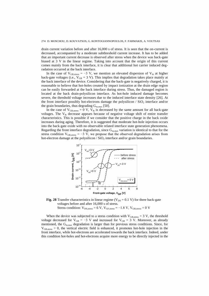
274 D. MOSCHOU, D. KOUVATSOS, G. KONTOGIANNOPOULOS, F. FARMAKIS, A. VOUTSAS
drain current variation before and after 16,000 s of stress. It is seen that the on-current is
decreased, accompanied by a moderate subthreshold current increase. It has to be added
that an important current decrease is observed after stress when the device was back-gate
biased at 3 V in the linear regime. Taking into account that the origin of this current
comes mainly from the back interface, it is clear that additional hot carrier induced deg-
radation occurred at the back interface.
In the case of VGB,stress = −3 V, we mention an elevated dispersion of Vth at higher
back-gate voltages (i.e., VGB = 3 V). This implies that degradation takes place mainly at
the back interface of the device. Considering that the back-gate is negatively charged, it is
reasonable to believe that hot-holes created by impact ionization at the drain edge region
can be easily forwarded at the back interface during stress. Thus, the damaged region is
located at the back drain-polysilicon interface. As hot-hole induced damage becomes
severe, the threshold voltage increases due to the induced interface state density [26]. At
the front interface possibly hot-electrons damage the polysilicon / SiO2 interface and/or
the grain boundaries, thus degrading Gm,max [50].
In the case of VGB,stress = 0 V, Vth is decreased by the same amount for all back-gate
voltages. The Vth decrease appears because of negative voltage shift of entire transfer
characteristics. This is possible if we consider that the positive charge in the back oxide
increases during aging. Therefore, it is suggested that moderate hot-hole injection occurs
into the back-gate oxide with no observable related interface state generation phenomena.
Regarding the front interface degradation, since Gm,max variation is identical to that for the
stress condition VGB,stress = −3 V, we propose that the observed degradation arises from
hot-electron damage at the polysilicon / SiO2 interface and/or grain boundaries.
-6 -4 -2 0 2 4 6 810
-14
10-12
10-10
10-8
10-6
10-4
VGB,stress
= 0 V
before stress
after stress
Dra
in c
urr
en
t, I
DS
[A
]
Front-gate voltage, VGF [V]
VGB
=3 V
VGB
=0 V
VGB
=-3 V
Fig. 28 Transfer characteristics in linear regime (VDS = 0.1 V) for three back-gate
voltages before and after 16,000 s of stress.
Stress condition: VDS,stress = 6 V, VGF,stress = −1.8 V, VGB,stress = 0 V
When the device was subjected to a stress condition with VGB,stress = 3 V, the threshold
voltage decreased for VGB = −3 V and increased for VGB = 3 V. Moreover, as already
mentioned, the Gm,max degradation is larger than for previous stress conditions. Since, for
VGB,stress > 0, the vertical electric field is enhanced, it promotes hot-hole injection in the
front interface, while hot-electrons are accelerated towards the back interface. Indeed, under
this condition hot-holes and hot-electrons acquire more energy to be directly injected in the

Technology, Performance and Degradation Characteristics of SLS ELA Thin Film Transistors 275
front- and in the back-gate oxide respectively. As a result, hot-hole induced interface state
generation is enhanced at the front interface, while electron injection at the back-gate oxide
provokes additional negative threshold voltage shift when measured at VGB = −3 V.
We proceeded to see whether there are differences in the degradation mechanisms of n-
channel and p-channel double gate TFTs of similar dimensions. The bottom gate was biased
at −3 V for n-channel devices and at 3 V for p- channel ones, to ensure that all current
carriers are pushed towards the top interface. Also, the drain stress biases were scaled with
the channel length of the devices to exclude the effect of different horizontal electrical field.
The stress condition used was Vdstress = Vth + 2 V for all DG TFTs. As we can see in Fig. 30,
for Gm,max degradation, we do not see any variation of the associated degradation
mechanisms, which concern trap generation within the polysilicon film (particularly at grain
boundaries). By reducing the top gate length in n-channel devices; this same mechanism is
more intense for larger length. For p-channel devices we see that in short channel devices
no significant degradation takes place. In devices having either kind of channel we see that
as the channel length increases, device degradation becomes more pronounced, due to the
incorporation of more sub-boundary traps within the channel area.
-6 -4 -2 0 2 4 6 810
-14
10-12
10-10
10-8
10-6
10-4
VGB
=0 V
VGB
=-3 V
VGB,stress
= -3 V
Dra
in c
urr
en
t, I
DS
[A
]
Front-gate voltage, VGF [V]
before stress
after stress
VGB
=3 V
Fig. 29 Transfer characteristics in linear regime (VDS = 0.1 V) for three back-gate volt-
ages before and after 16,000 s of stress.
Stress condition: VDS,stress = 6 V, VGF,stress = 3.5 V, VGB,stress = −3 V
a b
Fig. 30 Gm,max evolution with stress time in (a) p-channel and (b) n-channel double gate devices
10 100 1000 10000
0,0
1,0x10⁻⁶
2,0x10⁻⁶
3,0x10⁻⁶
4,0x10⁻⁶
5,0x10⁻⁶
6,0x10⁻⁶
Ltop
=0,5m
Ltop
=1,0m
Gm
,ma
x(A
/V)
stress time (sec)
10 100 1000 10000
0,0
2,0x10⁻⁶
4,0x10⁻⁶
6,0x10⁻⁶
8,0x10⁻⁶
1,0x10⁻⁵
1,2x10⁻⁵
1,4x10⁻⁵
1,6x10⁻⁵
Ltop
=0,5m
Ltop
=0,8m
Ltop
=1,3m
Gm
,max (
A/V
)
stress time (sec)

276 D. MOSCHOU, D. KOUVATSOS, G. KONTOGIANNOPOULOS, F. FARMAKIS, A. VOUTSAS
However, the threshold voltage Vth evolution with stressing time, shown in Fig. 31 for
n-channel DG TFTs, indicates that different associated degradation mechanisms, which
concern hot carrier injection into generated interface traps and/or the oxide bulk, are pre-
sent for varying top gate length in these devices. For Ltop = 0.5 μm we only observe a hot
electron injection induced Vth increase for larger stress times. For Ltop = 0.8 μm there is a
small initial Vth decrease, due to minor hole injection, followed by a pronounced increase
for even larger times. For Ltop = 1.3 μm the initial Vth reduction is much more pro-
nounced, again followed by a large increase for long stressing times. It is clear that the
initial hole injection mechanism is only present in long channel DG TFTs and becomes
more pronounced as the channel gets longer. Electron injection, however, is present in
DG TFTs having all top gate lengths and is always dominant for large stressing times.
This means that the former, but not the latter, is a channel length dependent degradation
mechanism. To further probe the nature of hot carrier injection we also investigated the
evolution of subthreshold slope S, which only reflects interface traps, with stress time,
and similar trends were observed. This indicates degradation by trap generation mainly at
the polysilicon – oxide interface and not by injection in the top gate oxide. The proposed
degradation mechanisms are supported by low frequency noise measurements [52].
Fig. 31 Threshold voltage Vth evolution with stress time for n-channel double gate TFTs
with different Ltop and Lbottom = 4 μm
5. CONCLUDING REMARKS AND PROSPECTS FOR SLS ELA TECHNOLOGY
A comprehensive investigation of the performance and degradation characteristics of
advanced LTPS TFTs fabricated using several variations of SLS ELA techniques, as re-
sulting from corresponding film microstructures and device geometries, has been pre-
sented. The polysilicon film grain structures resulting from these techniques were deter-
mined; directional films with elongated grains and various forms of films with engineered
grain shapes were obtained. The statistics of the electrical parameter values of TFTs fab-
ricated in such films were extracted. Furthermore, the parameter Vg,max – Vth was pro-
posed as a new measure of film trap density, in addition to Vth, μfe and S, that mainly
probes tail state generation, while S probes midgap states. The effects of the crystalliza-
10 100 1000 10000
0,5
1,0
1,5
2,0
2,5
3,0 Ltop
=0,5m
Ltop
=0,8m
Ltop
=1,3m
Vth (
V)
stress time (sec)
Technology, Performance and Degradation Characteristics of SLS ELA Thin Film Transistors 277
tion technique, grain boundaries, channel length and channel width on device character-
istics were investigated. Moreover, various TFT structures with top, bottom and double
gates, for the cases of both n-channel and p-channel devices, were studied and their pa-
rameters derived.
The degradation of SLS ELA TFTs fabricated with the aforementioned techniques
was investigated for various hot carrier and bias stress conditions. For directional films,
the polysilicon film thickness was found to affect which degradation mechanism is domi-
nant. Channel thickness and channel crystal quality are connected, as thicker films have
better quality, but were found to exert independent effects on TFT degradation; hot-car-
rier injection was the primary degradation mechanism for thinner TFTs (due to more car-
rier trapping, related to worse crystal quality) and for thicker ones (due to partial deple-
tion, related to thickness), while maximum degradation, associated with new defect crea-
tion, was only dominant for intermediate thickness (50 nm). Degradation was less pro-
nounced in the non-preferred Y direction, due to the harder sub-boundaries obstructing
the stress current. The main degradation mechanism for the X direction was interface
state generation, while for the Y direction the gate oxide charge injection. We also ob-
served channel shortening effect only in the X direction. Finally, an optimum channel
length was found, defined both by the process related sub-boundary characteristics and
by electrical effects.
For various kinds of SLS ELA films, the effects of channel type, width and orienta-
tion with respect to engineered grains, as well as the short channel effects were investi-
gated. A simple and practical degradation model was developed, taking into account the
formation of two regions, a defective and a non-defective one, in the stressed device. For
single-shot directional SLS ELA polysilicon TFTs, larger channel widths resulted in de-
vices exhibiting HCS degradation mainly due to more energetic hot electrons and thus
enhanced electron injection in the gate oxide, while for smaller widths hot-holes are
mainly responsible for the degradation. The quality characteristics of the width depended
degradation were evaluated by the model and the defective region length was found to
depend on channel width, with a different dependence for each stress regime studied. It was
found that the channel width affects the intensity and not the mechanism of degradation.
Furthermore, the degradation mechanisms pertaining to double gate TFTs were in-
vestigated and described. Various degradation mechanisms that depend on the back gate
voltage were identified and evaluated. Double gate TFTs for various channel lengths were
characterized; degradation was found to be more pronounced for longer channel devices,
due to the existence of more grain boundaries and sub-boundaries, resulting in more trap
generation. We observed two Vth degradation mechanisms, hole injection only in large
channel DG TFTs and electron injection in all devices for longer times; considering
additional S degradation data, these mechanisms were ascribed to interface trap generation.
As we can see from the previous analysis, the several variations of SLS ELA technol-
ogy can yield very high-performance and highly reliable TFTs, comparable to SOI tran-
sistors. This fact, with the added advantage of being able to integrate such devices on
various low temperature substrate materials (e.g. polymer, paper, foil etc), could open up
new prospects for high performance macroelectronic applications. Further integration
with other low-temperature devices (e.g. OLEDs) could allow stretchable or foldable,
high performance commercial electronics, since the excellent SLS ELA TFT characteris-
tics allow for advanced CMOS circuit design. Also, high performance TFTs could allow
for their utilization as versatile (due to the freedom to choose a substrate of choice other
278 D. MOSCHOU, D. KOUVATSOS, G. KONTOGIANNOPOULOS, F. FARMAKIS, A. VOUTSAS
than Si wafers) physical, chemical or biological sensors. Their optimum mobility can
yield very sensitive, and highly conducive to integration, sensing devices, possibly al-
lowing for "smarter" micro Total Analysis Systems (μTAS) with the integration of mi-
crofluidic networks.
REFERENCES
[1] T. Matsuo and T. Muramatsu, "21.1: Invited Paper: CG Silicon Technology and Development of System
on Panel", in SID Symposium Digest of Technical Papers, 2004, pp. 856-859.
[2] S. Brotherton, D. McCulloch, J. Clegg, and J. Gowers, "Excimer-laser-annealed poly-Si thin-film transistors", Electron Devices, IEEE Transactions on, vol. 40, pp. 407-413, 1993.
[3] R. S. Sposili and J. S. Im, "Sequential lateral solidification of thin silicon films on SiO2", Applied Physics
Letters, vol. 69, pp. 2864-2866, 1996. [4] A. T. Voutsas, "Assessment of the performance of laser-based lateral-crystallization technology via
analysis and modeling of polysilicon thin-film-transistor mobility", Electron Devices, IEEE Transactions on, vol. 50, pp. 1494-1500, 2003.
[5] P. Mei, J. Boyce, M. Hack, R. Lujan, S. Ready, D. Fork, et al., "Grain growth in laser dehydrogenated
and crystallized polycrystalline silicon for thin film transistors", Journal of Applied Physics, vol. 76, pp. 3194-3199, 1994.
[6] W.-C. Yeh and M. Matsumura, "Preparation of giant-grain seed layer for poly-silicon thin-film solar
cells", Japanese Journal of Applied Physics, vol. 38, pp. L110-L112, 1999. [7] T. Mizuki, J. S. Matsuda, Y. Nakamura, J. Takagi, and T. Yoshida, "Large domains of continuous grain
silicon on glass substrate for high-performance TFTs", Electron Devices, IEEE Transactions on, vol. 51,
pp. 204-211, 2004. [8] H. Hayashi, M. Kunii, N. Suzuki, Y. Kanaya, M. Kuki, M. Minegishi, et al., "Fabrication of Low-
temperature bottom-gate Poly-Si TFTs on large-area substrate by linear-beam excimer laser crystallization
and ion doping method", in Electron Devices Meeting, 1995, International, pp. 829-832, 1995. [9] I.-H. Song and M.-K. Han, "Low temperature poly-Si TFTs for display application", Current Applied
Physics, vol. 3, pp. 363-366, 2003.
[10] J. Y. Seto, "The electrical properties of polycrystalline silicon films", Journal of Applied Physics, vol. 46, pp. 5247-5254, 1975.
[11] D. C. Moschou, D. N. Kouvatsos, F. V. Farmakis, and A. T. Voutsas, "Characterization of advanced
directional SLS ELA polysilicon TFTs", in ITC 2007, 2007. [12] G. Kontogiannopoulos, D. Moschou, D. Kouvatsos, G. Papaioannou, and A. Voutsas, "Short channel
effects in SLS ELA polysilicon TFTs", in Proceedings of ITC, pp. 70-3, 2009.
[13] D. C. Moschou, M. Exarchos, D. N. Kouvatsos, G. Papaioannou, and A. T. Voutsas, "Performance and reliability of SLS ELA polysilicon TFTs fabricated with novel crystallization techniques",
Microelectronics Reliability, vol. 47, pp. 1378-1383, 2007.
[14] D. C. Moschou, N. Vourdas, D. Davazoglou, D. N. Kouvatsos, V. E. Vamvakas, and A. T. Voutsas, "On the optical properties of SLS ELA polycrystalline silicon films", Microelectronic Engineering, vol. 90,
pp. 69-71, 2012.
[15] D. N. Kouvatsos, F. V. Farmakis, D. C. Moschou, G. P. Kontogiannopoulos, G. J. Papaioannou, and A.
T. Voutsas, "Characterization of double gate TFTs fabricated in advanced SLS ELA polycrystalline
silicon films", Solid-State Electronics, vol. 51, pp. 936-940, 2007.
[16] D. C. Moschou, G. P. Kontogiannopoulos, D. N. Kouvatsos, and A. T. Voutsas, "On the importance of the Vg,max – Vth parameter on LTPS TFT stressing behavior", Microelectronics Reliability, vol. 50, pp.
190-194, 2010.
[17] N. Yamauchi, J. J. J. Hajjar, and R. Reif, "Polysilicon thin-film transistors with channel length and width comparable to or smaller than the grain size of the thin film", Electron Devices, IEEE Transactions on,
vol. 38, pp. 55-60, 1991.
[18] N. Yamauchi, J. J. J. Hajjar, R. Reif, K. Nakazawa, and K. Tanaka, "Characteristics of narrow-channel polysilicon thin-film transistors", Electron Devices, IEEE Transactions on, vol. 38, pp. 1967-1968, 1991.
[19] D. N. Yaung, Y. K. Fang, K. C. Hwang, K. Y. Lee, K. H. Wu, J. J. Ho, et al., "Narrow width effects of
bottom-gate polysilicon thin film transistors", Electron Device Letters, IEEE, vol. 19, pp. 429-431, 1998.
Technology, Performance and Degradation Characteristics of SLS ELA Thin Film Transistors 279
[20] D. C. Moschou, M. Exarchos, D. Kouvatsos, G. Papaioannou, and A. Voutsas, "A novel SLS ELA
crystallization process and its effects on polysilicon film defectivity and TFT performance", Microelectronic Engineering, vol. 85, pp. 1447-1452, 2008.
[21] F. Farmakis, D. Kouvatsos, A. Voutsas, D. Moschou, G. Kontogiannopoulos, and G. Papaioannou,
"Front and back channel properties of asymmetrical double-gate polysilicon TFTs", Journal of The Electrochemical Society, vol. 154, pp. H910-H913, 2007.
[22] M. Exarchos, D. Moschou, G. Papaioannou, D. Kouvatsos, A. Arapoyanni, and A. Voutsas, "On the
study of p-channel thin-film transistors fabricated by SLS ELA crystallization techniques", Thin Solid Films, vol. 517, pp. 6375-6378, 2009.
[23] D. C. Moschou, M. Exarchos, D. N. Kouvatsos, G. Papaioannou, A. Arapoyanni, and A. T. Voutsas,
"Reliability and defectivity comparison of n-and p-channel SLS ELA polysilicon TFTs fabricated with a novel crystallization technique", Microelectronics Reliability, vol. 48, pp. 1544-1548, 2008.
[24] A. Voutsas, D. Kouvatsos, L. Michalas, and G. Papaioannou, "Effect of silicon thickness on the
degradation mechanisms of sequential laterally solidified polycrystalline silicon TFTs during hot-carrier stress", Electron Device Letters, IEEE, vol. 26, pp. 181-184, 2005.
[25] K. M. Chang, Y. H. Chung, G. M. Lin, C. G. Deng, and J. H. Lin, "Enhanced degradation in
polycrystalline silicon thin-film transistors under dynamic hot-carrier stress", Electron Device Letters, IEEE, vol. 22, pp. 475-477, 2001.
[26] F. Farmakis, J. Brini, G. Kamarinos, and C. Dimitriadis, "Anomalous turn-on voltage degradation during
hot-carrier stress in polycrystalline silicon thin-film transistors", Electron Device Letters, IEEE, vol. 22, pp. 74-76, 2001.
[27] G. Armstrong, S. Uppal, S. Brotherton, and J. Ayres, "Differentiation of effects due to grain and grain
boundary traps in laser annealed poly-Si thin film transistors", Jap. J. Appl. Phys, vol. 37, 1998. [28] B. S. Doyle, M. Bourcerie, C. Bergonzoni, R. Benecchi, A. Bravis, K. R. Mistry, et al., "The generation and
characterization of electron and hole traps created by hole injection during low gate voltage hot-carrier
stressing of n-MOS transistors", Electron Devices, IEEE Transactions on, vol. 37, pp. 1869-1876, 1990. [29] P. Heremans, R. Bellens, G. Groeseneken, and H. E. Maes, "Consistent model for the hot-carrier
degradation in n-channel and p-channel MOSFETs", Electron Devices, IEEE Transactions on, vol. 35,
pp. 2194-2209, 1988. [30] A. Voutsas, A. Limanov, and J. Im, "Effect of process parameters on the structural characteristics of
laterally grown, laser-annealed polycrystalline silicon films", Journal of Applied Physics, vol. 94, pp.
7445-7452, 2003. [31] J. Levinson, F. Shepherd, P. Scanlon, W. Westwood, G. Este, and M. Rider, "Conductivity behavior in
polycrystalline semiconductor thin film transistors", Journal of Applied Physics, vol. 53, pp. 1193-1202, 1982.
[32] J.-P. Colinge, Silicon-on-insulator technology: materials to VLSI: Kluwer Academic Pub, 1997. [33] G. P. Kontogiannopoulos, F. V. Farmakis, D. N. Kouvatsos, G. J. Papaioannou, and A. T. Voutsas, "Hot-
carrier stress induced degradation of SLS ELA polysilicon TFTs–Effects of gate width variation and
device orientation", Solid-State Electronics, vol. 52, pp. 388-393, 2008. [34] D. Moschou, D. Kouvatsos, I. Pappas, C. Dimitriadis, and A. Voutsas, "Short channel effects in double
gate polycrystalline silicon SLS ELA TFTs", in Microelectronics (MIEL), 2012 28th International Conference on, pp. 91-94, 2012.
[35] E. Takeda, C. Y.-W. Yang, and A. Miura-Hamada, Hot-carrier effects in MOS devices: Access Online
via Elsevier, 1995. [36] N. Young, A. Gill, and M. Edwards, "Hot carrier degradation in low temperature processed polycrystalline
silicon thin film transistors", Semiconductor Science and Technology, vol. 7, p. 1183, 1992.
[37] Y. Leblebici, "Design considerations for CMOS digital circuits with improved hot-carrier reliability", Solid-State Circuits, IEEE Journal of, vol. 31, pp. 1014-1024, 1996.
[38] S.-M. Kang and Y. Leblebici, Cmos Digital Integrated Circuits, 3/E: Tata McGraw-Hill Education, 2003.
[39] M. Hack, A. G. Lewis, and I.-W. Wu, "Physical models for degradation effects in polysilicon thin-film transistors", Electron Devices, IEEE Transactions on, vol. 40, pp. 890-897, 1993.
[40] A. T. Hatzopoulos, D. H. Tassis, N. A. Hastas, C. A. Dimitriadis, and G. Kamarinos, "An analytical hot-
carrier induced degradation model in polysilicon TFTs", Electron Devices, IEEE Transactions on, vol. 52, pp. 2182-2187, 2005.
[41] H. Haddara and S. Cristoloveanu, "Two-dimensional modeling of locally damaged short-channel
MOSFET's operating in the linear region", Electron Devices, IEEE Transactions on, vol. 34, pp. 378-385, 1987.
[42] K. N. Quader, C. C. Li, R. Tu, E. Rosenbaum, P. Ko, and C. Hu, "A bidirectional NMOSFET current
reduction model for simulation of hot-carrier-induced circuit degradation", Electron Devices, IEEE Transactions on, vol. 40, pp. 2245-2254, 1993.
280 D. MOSCHOU, D. KOUVATSOS, G. KONTOGIANNOPOULOS, F. FARMAKIS, A. VOUTSAS
[43] C. Wie, Z. Tang, and M. Park, "Nonuniform threshold voltage profile in a-Si:H thin film transistors stressed
under both gate and drain biases", Journal of Applied Physics, vol. 104, pp. 114509-114509-8, 2008. [44] Y.-H. Lee, K. Wu, T. Linton, N. Mielke, S. Hu, and B. Wallace, "Channel-width dependent hot-carrier
degradation of thin-gate pMOSFETs", in Reliability Physics Symposium, 2000. Proceedings. 38th Annual
2000 IEEE International, pp. 77-82, 2000. [45] G. P. Kontogiannopoulos, F. V. Farmakis, D. N. Kouvatsos, G. J. Papaioannou, and A. T. Voutsas, "A
Practical Model Assessing the Degradation of Polycrystalline Silicon TFTs Due to DC Electrical Stress",
Electron Devices, IEEE Transactions on, vol. 57, pp. 1390-1398, 2010. [46] F. V. Farmakis, J. Brini, G. Kamarinos, C. T. Angelis, C. A. Dimitriadis, and M. Miyasaka, "On-current
modeling of large-grain polycrystalline silicon thin-film transistors", Electron Devices, IEEE
Transactions on, vol. 48, pp. 701-706, 2001. [47] K. Rais, G. Ghibaudo, and F. Balestra, "Surface roughness mobility model for silicon MOS transistors",
Physica Status Solidi (a), vol. 146, pp. 853-858, 1994.
[48] Z. Tang, M. Park, S. Jin, and C. Wie, "Drain bias dependent bias temperature stress instability in a-Si: H TFT", Solid-State Electronics, vol. 53, pp. 225-233, 2009.
[49] C. A. Dimitriadis, M. Kimura, M. Miyasaka, S. Inoue, F. V. Farmakis, J. Brini, et al., "Effect of grain
boundaries on hot-carrier induced degradation in large grain polysilicon thin-film transistors", Solid-State Electronics, vol. 44, pp. 2045-2051, 2000.
[50] S. Cristoloveanu, "Hot-carrier degradation mechanisms in silicon-On-Insulator MOSFETS",
Microelectronics Reliability, vol. 37, pp. 1003-1013, 1997. [51] F. V. Farmakis, G. P. Kontogiannopoulos, D. N. Kouvatsos, and A. T. Voutsas, "Degradation of double-
gate polycrystalline silicon TFTs due to hot carrier stress", Microelectronics Reliability, vol. 47, pp.
1434-1438, 2007. [52] D. C. Moschou, C. G. Theodorou, N. A. Hastas, A. Tsormpatzoglou, D. N. Kouvatsos, A. T. Voutsas, et
al., "Short Channel Effects on LTPS TFT Degradation", Journal of Display Technology, vol. 9, pp. 747-
754, 2013.