technology roadmap document for ska signal processing · pdf filew. turner signal processing...
TRANSCRIPT

Name Designation Affiliation Date Signature
Additional Authors
Submitted by:
W. Turner Signal Processing Domain Specialist
SPDO 2011‐03‐26
Approved by:
P. Dewdney Project Engineer SPDO 2010‐03‐29
TECHNOLOGY ROADMAP DOCUMENT FOR SKA SIGNAL
PROCESSING
Document number .................................................................. WP2‐040.030.011‐TD‐001
Revision ........................................................................................................................... 1
Author ................................................................................................................ W.Turner
Date ................................................................................................................ 2011‐02‐27
Status ....................................................................................................................... Issued

WP2‐040.030.011‐TD‐001 Revision : 1
2011‐02‐27 Page 2 of 71
DOCUMENT HISTORY
Revision Date Of Issue Engineering Change
Number
Comments
1 ‐ ‐ First issue
DOCUMENT SOFTWARE
Package Version Filename
Wordprocessor MsWord Word 2007 02‐WP2‐040.030.011.TD‐001‐1_SKATechnologyRoadmap
Block diagrams
Other
ORGANISATION DETAILS
Name SKA Program Development Office
Physical/Postal
Address
Jodrell Bank Centre for Astrophysics
Alan Turing Building
The University of Manchester
Oxford Road
Manchester, UK
M13 9PL
Fax. +44 (0)161 275 4049
Website www.skatelescope.org

WP2‐040.030.011‐TD‐001 Revision : 1
2011‐02‐27 Page 3 of 71
TABLE OF CONTENTS
1 INTRODUCTION ............................................................................................. 9
1.1 Purpose of the document ....................................................................................................... 9
1.2 Technology Readiness Levels ................................................................................................ 10
2 REFERENCES .............................................................................................. 12
3 PROCESSING .............................................................................................. 14
3.1 General Purpose Processor ................................................................................................... 14
3.1.1 Theoretical Processing Performance ............................................................................ 17
3.1.2 Cost ............................................................................................................................... 17
3.1.3 Thermal Dissipation ...................................................................................................... 17
3.1.4 Scalability ...................................................................................................................... 18
3.2 Graphics Processing Unit ...................................................................................................... 19
3.2.1 Intel ............................................................................................................................... 19
3.2.2 ATI (AMD) ...................................................................................................................... 21
3.2.3 NVIDIA ........................................................................................................................... 22
3.2.4 Theoretical Processing Performance ............................................................................ 23
3.2.5 Cost ............................................................................................................................... 24
3.2.6 Thermal Dissipation ...................................................................................................... 24
3.3 Field Programmable Gate Array............................................................................................ 25
3.3.1 Theoretical Processing Performance ............................................................................ 28
3.3.2 Cost ............................................................................................................................... 28
3.3.3 Thermal Dissipation ...................................................................................................... 30
3.3.4 Hard Copy ...................................................................................................................... 31
3.4 Application Specific Integrated Circuit ASIC ......................................................................... 31
3.4.1 Process Size ................................................................................................................... 31
3.4.2 Masking Costs ............................................................................................................... 35
3.4.3 Yield and Die Costs ........................................................................................................ 35
3.4.4 Prototyping ................................................................................................................... 37
3.5 Gap between FPGAs and ASICS ............................................................................................. 37
3.5.1 Theoretical Processing Performance ............................................................................ 38
3.5.2 Cost ............................................................................................................................... 38
3.5.3 Thermal Dissipation ...................................................................................................... 39
3.6 Network on Chip, NoC........................................................................................................... 39
4 STORAGE .................................................................................................. 42
4.1 SRAM ..................................................................................................................................... 45
4.1.1 SRAM performance ....................................................................................................... 46
4.1.2 SRAM Thermal Dissipation ............................................................................................ 46
4.1.3 SRAM Cost ..................................................................................................................... 46
4.2 Dynamic Random Access Memory, DRAM ........................................................................... 46

WP2‐040.030.011‐TD‐001 Revision : 1
2011‐02‐27 Page 4 of 71
4.2.1 DRAM Performance ...................................................................................................... 47
4.2.2 DRAM Cost .................................................................................................................... 48
4.2.3 DRAM Thermal Dissipation ........................................................................................... 49
4.3 Flash Memory ....................................................................................................................... 50
4.3.1 NAND Cost ..................................................................................................................... 52
4.3.2 NAND Thermal Dissipation ............................................................................................ 52
4.4 Storage Class Memory .......................................................................................................... 52
4.4.1 SCM Performance ......................................................................................................... 53
4.4.2 SCM Cost ....................................................................................................................... 54
4.4.3 SCM Thermal Dissipation .............................................................................................. 54
5 DISK STORAGE ............................................................................................ 54
5.1.1 Disk Performance .......................................................................................................... 55
5.1.2 Disk Thermal Dissipation ............................................................................................... 56
5.1.3 Disk Cost ........................................................................................................................ 56
6 NETWORK ................................................................................................. 57
6.1 Infiniband .............................................................................................................................. 57
6.1.1 Infiniband Performance Roadmap ................................................................................ 57
6.1.2 Host Channel Adapters ................................................................................................. 58
6.1.3 Infiniband switches ....................................................................................................... 58
6.2 Ethernet ................................................................................................................................ 59
6.2.1 100 G bit/s Ethernet Switches ...................................................................................... 60
6.2.2 Terabit Ethernet ............................................................................................................ 60
6.2.3 Ethernet Cost ................................................................................................................ 60
6.2.4 Ethernet Thermal Dissipation ....................................................................................... 60
6.3 Optical Interconnect ............................................................................................................. 61
6.3.1 Performance.................................................................................................................. 63
6.3.2 Thermal Dissipation ...................................................................................................... 64
6.3.3 Cost ............................................................................................................................... 64
7 APPENDIX 1 ............................................................................................... 64
7.1 Moore’s Law .......................................................................................................................... 64
7.2 Transistor Size ....................................................................................................................... 66
7.3 Breaking Moore’s Law ........................................................................................................... 67
7.4 Moore’s Law and Processing Capability ................................................................................ 67
8 APPENDIX 2 ............................................................................................... 68
8.1 Tilera ..................................................................................................................................... 68
8.2 Clearspeed ............................................................................................................................ 69
8.3 PicoChip................................................................................................................................. 70
8.4 Other Technologies ............................................................................................................... 71

WP2‐040.030.011‐TD‐001 Revision : 1
2011‐02‐27 Page 5 of 71
LIST OF FIGURES
Figure 1 Computations per kilowatt hour over time ............................................................................ 15
Figure 2 Intel’s Tick Tock Roadmap ....................................................................................................... 16
Figure 3 Parallel speed up ..................................................................................................................... 18
Figure 4 Intel’s Science Computing Road‐Map ..................................................................................... 20
Figure 5 Intel Roadmap ......................................................................................................................... 20
Figure 6 ATI Graphics accelerator with 8 GPU cards ............................................................................ 21
Figure 7 NVIDIA GPU Historic Roadmap ............................................................................................... 22
Figure 8 NVIDIA Tesla S2050unit plan view .......................................................................................... 23
Figure 9 Tesla S2050 Architecture ........................................................................................................ 23
Figure 10 CUDA GPU Processing power per Watt Road‐map ............................................................... 24
Figure 11 Gates per unit area of silicon as a function of process size .................................................. 32
Figure 12 IBM ASIC Gate Delays ............................................................................................................ 32
Figure 13 IBM ASIC Dynamic Power...................................................................................................... 33
Figure 14IBM ASIC Static Power ........................................................................................................... 34
Figure 15 Total chip dynamic and static power dissipation trends ...................................................... 34
Figure 16 Mask Tooling Costs ............................................................................................................... 35
Figure 17 Example NoC and processing Tile ......................................................................................... 40
Figure 18 Silicon Implementation ......................................................................................................... 40
Figure 19 Artist’ concept of 3D silicon processor chip with optical IO layer featuring on‐chip
nanophotonic network ............................................................................................................... 42
Figure 20 Storage taxonomy ................................................................................................................. 43
Figure 21 Storage Hierarchy.................................................................................................................. 44
Figure 22 Samsung’s Memory Technology and Solutions Roadmap .................................................... 44
Figure 23 Samsung’s DRAM Historic Roadmap ..................................................................................... 47
Figure 24 Samsung’s DRAM Historic Roadmap ..................................................................................... 47
Figure 25 Samsung DDR DRAM Performance Roadmap ...................................................................... 48
Figure 26 DRAM Chip Selling Price December 2010 ............................................................................. 49
Figure 27 Samsung DRAM: Measured Thermal Dissipation ................................................................. 49
Figure 28 NAND and NOR Flash Memory Schematics and Cell layout ................................................. 50
Figure 29 Intel Micron Historic Flash Roadmap .................................................................................... 51
Figure 30 NAND Cost per M Byte Road Map ........................................................................................ 52
Figure 31 SCM Roadmap in relation to NAND, DRAM and Hard Disk (HDD) ........................................ 54
Figure 32 Historic Roadmap for Disk Areal Density .............................................................................. 55
Figure 33 Historic Roadmap for Disk Bandwidth .................................................................................. 55
Figure 34 Infiniband Roadmap .............................................................................................................. 58
Figure 35 Ethernet PHY standards ........................................................................................................ 59
Figure 36 Alcatel Lucent Power Consumption Roadmap ..................................................................... 61
Figure 37 CFP Hardware Specification Power Interlock........................................................................ 61
Figure 38 IBM Terra Bus Overview ....................................................................................................... 62
Figure 39 IBM Terrabus Integrated Circuit Connectivity ...................................................................... 63
Figure 40 IBM Terrabus Integrated Circuit and Printed Circuit board Optical Connectivity ................ 63

WP2‐040.030.011‐TD‐001 Revision : 1
2011‐02‐27 Page 6 of 71
Figure 41 Numbers of Transistors for Intel Processors ......................................................................... 64
Figure 42 ITRS transistor cost predictions ............................................................................................ 65
Figure 43 Roadmap of Transistor Size .................................................................................................. 66
Figure 44 Physical Scaling of Parameters for a Semi‐conductor gate .................................................. 67
Figure 45 Tilera Tile Processor architecture ......................................................................................... 69
Figure 46 Clearspeed’s CSX 700 ............................................................................................................ 70
Figure 47 PicoChip’s Pico Array Architecture. ...................................................................................... 71
LIST OF TABLES
Table 1 Technology readiness levels as risk likelihood indicators ........................................................ 10
Table 2 Technology Readiness Level Definitions .................................................................................. 11
Table 3 Intel’s Tick Tock Time Line ........................................................................................................ 16
Table 4 Xilinx Current Virtex 6 product range ....................................................................................... 26
Table 5 Xilinx Next Generation FPGA (Virtex 7) .................................................................................... 27
Table 6 Xilinx pricing on 29th December 2010 for Virtex 6 Devices ...................................................... 29
Table 7 FPGA to ASIC Gap Summary ..................................................................................................... 37
Table 8 NoC Packet transmission Energies ........................................................................................... 41
Table 9 Current Baseline and Prototypical Memory Technologies (ITRS 2007) ................................... 45
Table 10 Semiconductor parameter growth ......................................................................................... 65
Table 11 Device Scaling factors ............................................................................................................. 66

WP2‐040.030.011‐TD‐001 Revision : 1
2011‐02‐27 Page 7 of 71
LIST OF ABBREVIATIONS
AA .................................. Aperture Array
Ant. ................................ Antenna
API ................................. Application Programming Interface
ASIC .............................. Application Specific Integrated Circuit
BER ............................... Bit Error Rate
CAD ............................... Computer Aided Design
CAGR ............................ Compound Annual Growth Rate
CoDR ............................. Conceptual Design Review
COTS ............................ Commercial off te Shelf
cm .................................. centmetre
CPU ............................... Central Processing Unit
DDR ............................... Double Data Rate
DOD .............................. Department of Defence
DRAM ............................ Dynamic Random Access Memory
DRM .............................. Design Reference Mission
DSP ............................... Digital Signal Processor
EDA ............................... Electronic Design Automation
EoR ............................... Epoch of Reionisation
EX .................................. Example
FFT ................................ Fast Fourier Transform
FLOPS ........................... Floating Point Operations per second
FoV ................................ Field of View
FPGA ............................. Field Programmable Gate Array
GPU ............................... Graphics Processing Unit
HCA ............................... Host Channel Adapter
HDD ............................... Hard Disk Drive
HDL ............................... High Definition Language
HDR ............................... High Data Rate
Hz .................................. Herz
IDR ................................ Internal Data Rate
IFFT ............................... Inverse Fast Fourier Transform
I/O .................................. input/ output
IP ................................... Intellectual Property
K .................................... Kelvin
LNA ............................... Low Noise Amplifier
MAC .............................. Multiply Accumulate
MLM .............................. Multi-Layer Mask

WP2‐040.030.011‐TD‐001 Revision : 1
2011‐02‐27 Page 8 of 71
MMF .............................. Multi Mode Fibre
MPW .............................. Multi-Project Wafer
MW ................................ Mega Watt
nm ................................. nano metre
NoC ............................... Network on Chip
NDA ............................... Non Disclosure Agreement
NDR ............................... Next Data Rate
NRE ............................... Non Recurring Engineering
Ny .................................. Nyquist
OH ................................. Over Head
ONoC ............................ Optical Network on Chip
OS ................................. Operating System
OTPF ............................. Observing Time Performance Factor
Ov .................................. Over sampling
PAF ............................... Phased Array Feed
PCI ................................ Peripheral Component Interconect
PCIe .............................. PCI Express
PrepSKA........................ Preparatory Phase for the SKA
Rd .................................. read
RFI ................................. Radio Frequency Interference
rms ................................ root mean square
RRAM ............................ Resistive Random Access Memory
SCM .............................. Storage Centric Memory
SEFD...........................System Equivalent Flux Density
SER ............................... Soft Error Rate
SKA ............................... Square Kilometre Array
SKA1 ............................. SKA Phase 1
SKA2 ............................. SKA Phase 2
SKADS .......................... SKA Design Studies
SMF ............................... Single Mode Fibre
SPDO ............................ SKA Program Development Office
SRAM ............................ Static Random Access Memory
SSD ............................... Solid State Drive
SSFoM .......................... Survey Speed Figure of Merit
TBD ............................... To be decided
TRL ................................ Technology Readiness Level
Wr .................................. write
Wrt ................................. with respect to

WP2‐040.030.011‐TD‐001 Revision : 1
2011‐02‐27 Page 9 of 71
1 Introduction
The aim of this document is provide an overview of the technology that could potentially form the
basis of the signal processing for the SKA telescope. It is intended that this document should be
reviewed and updated on an annual basis leading up to phase 1 and phase 2 of the telescope to
provide an up to date perspective as input to the technology selection process. This is intended to
be a complementary activity abstracted from specific Concept Designs. Consequently, the document
focus is the technology options and their attributes rather than design details. It is intended that the
document should provide a wide coverage of technology; however, the level of detail provided on
specific technologies will be proportional to the perceived relevance of the technology at the time of
writing.
One limitation of this document is that its scope is restricted to information available in the public
domain. For obvious reasons, commercial manufacturers tend to be quite guarded about their
specific road maps and may only release details under Non Disclosure Agreements, NDAs. However,
this is not considered a major limitation in providing a reasonable overview for a technology
roadmap particularly one that is to be updated on an annual basis.
This document is part of a series generated in support of the Signal Processing CoDR which includes
the following:
Signal Processing High Level Description
Technology Roadmap
Design Concept Descriptions
Signal Processing Requirements
Signal Processing Costs
Signal Processing Risk Register
Signal Processing Strategy to Proceed to the Next Phase
Signal Processing Co DR Review Plan
Software & Firmware Strategy
1.1 Purpose of the document
The overall purpose of this document is to identify the road map of processing and communication
technology applicable to the SKA signal processing. This is to include:
Identify known potential technologies applicable to the SKA
Where possible project attributes of known technology to the time frame of the SKA in
terms of:
o Performance
o Cost

WP2‐040.030.011‐TD‐001 Revision : 1
2011‐02‐27 Page 10 of 71
o Thermal Dissipation
Provide an overview of potential future technologies that may be applicable to the SKA
within the time frame of the SKA1 or SKA2.
List ‘also ran’ technologies that have been considered but have been considered unsuitable
in their current format
1.2 Technology Readiness Levels
For a document detailing a technology roadmap the issue of technology readiness needs to be
raised. The Risk Management PLAN MGT‐040.040.000‐MP‐001 iss 1 proposes that a condensed
version of the United States Department of Defence (DOD) and NASA technology readiness levels
(TRL) be used to estimate the likelihood of occurrence for the relevant technology and these are
shown in Table 1
Table 1 Technology readiness levels as risk likelihood indicators
It is important to note that the technology readiness may differ from one hierarchical level to the
next. For example ‐ individual components may be freely available implying that the risk for
procurement at the component level is low. However, if these components have not yet been
integrated and shown to fulfil the required functions in the required environment at the next
hierarchical level, the risk at this higher level will be high.
The definitions of the technology readiness levels are shown in Table 2. These definitions should be
taken into account along with the risk likelihood level when using the roadmap to inform any
concept implementation.

WP2‐040.030.011‐TD‐001 Revision : 1
2011‐02‐27 Page 11 of 71
Table 2 Technology Readiness Level Definitions
WP2‐040.030.011‐TD‐001 Revision : 1
2011‐02‐27 Page 12 of 71
2 References
[1] International Technology Roadmap for Semiconductors (ITRS), available at www.itrs.net.
[2] Terrabus: a Chip‐to‐Chip Parallel Optical Interconnect J A Kash et al.
[3] Progress in Digital Integrated Electronics G Moore Technical Digest‐IEEE Int’l Electronic
Devices Meeting Vol 21 1975 pp 11‐13
[4] Establishing Moore’s Law Ethan Mollick IEEE Annals of the History of Computing vol 28 No. 3
2006 pp 62 ‐ 75
[5] Three Steps to the Thermal Noise Death of Moore’s Law Jacek Izydorczyk IEEE trans VLSI
Systems Vol 18 No.1 2010 pp 161 ‐ 165
[6] Limits to Binary Logic Switch Scaling—A Gedanken Model Victor V. Zhirnov et al Proc. IEEE
vol 91 no 11 2003 pp 1934 ‐ 1939
[7] Limits on Silicon Nanoelectronics for Terascale Integration J. D Meindl Vol293 Science
[8] Microprocessor Scaling: What Limits Will Hold? Jacek Izydorczyk IEEE Computer Aug 2010
[9] Emerging Research Memory and Logic Technology J A Hutchby et al. IEEE Circuits & Devices
Magazine vol 21 No. 3 2005 pp 47 – 51
[10] Future Trends in Microelectronics S Luryi, J Xu & A Zaslavsky John Wiley & Sons
[11] The High‐K Solution M T Bohr, R Chau & K Mistry IEEE Spectrum vol 44 No. 10 2007 pp 29‐
35
[12] Quantifying and Exploring the Gap Between FPGAs and ASICS Ian Kuon & Jonathan Rose
Springer
[13] Explaining the gap between ASIC and custom power: a custom perspective A Chang, W J
Dally DAC ’05 Proceedings of the 42nd annual conference on Design automation pp 281 –
284 ACM New York 2005
[14] Closing the Gap Between ASIC & Custom Tools and Techniques for High‐Performance ASIC
Design D.Chinnery, K Keutzer Kluwer New York 2002
[15] Closing the Power Gap Between ASIC and Custom: an ASIC perspective. DAC ’05 Proceedings
of the 42nd annual conference on Design automation pp 275 – 280 ACM New York 2005
[16] The role of custom design in ASIC chips DAC ’00 Proceedings of the 37th annual conference
on Design automation pp 643 – 647 ACM New York 2005
[17] J G. Koomey Assessing Trends in the Electrical Efficiency of Computation Over Time report
to Microsoft and Intel Corporations
[18] Computer Architecture a Quantitative Approach Hennessy and Patterson
[19] A 51mW 1.6 GHz on‐chip network for low‐power heterogeneous SoC platform Kangmin Lee
et al, IEEE Int. Solid‐States Circuit Conference, Digest of Technical papers, pp 152‐512 Feb
2004
[20] An 800MHz star‐connected on‐chip network for application to systems on a chip: Se‐Joong
Lee et al, IEEE Int. Solid‐States Circuits Conf. Digest of Technical papers, pp.468‐469 Feb 2003
[21] Low‐Power NoC for High‐Performance SoC Design, Hoi‐Jun Yoo, Kangmin Lee, Jun Kyoung
Kim, CRC Press 2008
An 80‐Tile 1 .28 TFLOPS Network‐on‐Chip in 65nm CMOS, Sriram Vangali, Jason Howard, Gregory
Ruhl, Saurabh Dighe, Howard Wilson, James Tschanz, David Finan, Priya Iyerl, Arvind Singh, Tiju

WP2‐040.030.011‐TD‐001 Revision : 1
2011‐02‐27 Page 13 of 71
Jacob, Shailendra Jain, Sriram Venkataraman, Yatin Hoskote, Nitin Borkar ISSCC 2007/1 Session 5/1
Microprocessors / 52

WP2‐040.030.011‐TD‐001 Revision : 1
2011‐02‐27 Page 14 of 71
3 Processing
The scale of the SKA Signal Processing has some onerous processing and signal transport
requirements due to its sheer scale whilst being constrained by cost and thermal dissipation.
Of the potential solutions, four processing technologies are currently popular with astronomy
engineering community and potentially offers solutions within the timeframe of the SKA:
General Purpose Processor
GPU
FPGA
ASIC
However, there are other interesting developments that aren’t in the mainstream that could
potentially pave the way to a solution. The Appendix details some of these options.
3.1 General Purpose Processor
The term general purpose processor is nominally used to identify x86 architecture processors
manufactured by Intel and AMD and are typically programmed in a high level language. Other
processors also fall into this category such as Motorola’s Vector processing and Sun’s Niagara. Each
of these processors is aimed at providing a highly flexible programming platform coupled to a
supporting an Operating System, OS. One cost of providing this general purpose capability is the
power efficiency of the platform that requires extra hardware to support the inbuilt flexibility. For
example, the processing unit will typically be 32 or 64 bit floating point irrespective of the data word
length. A metric typically used to indicate the processing efficiency is processing capability per
kilowatt, kW.
Figure 1 details the roadmap of the theoretical processing capability per kW hour of dissipation for
general purpose computer over the period 1945 through to 2010. Projecting from this graph
suggests 2.7 x 10¹⁶ computations per kW hour by 2015 or alternatively 7.5 x 10¹⁵ computations per
second per Mega watt dissipation. An industry target of ~20 MW exists for Exascale computing by
2020. This can be shown to be consistent with projections from Figure 1.

WP2‐040.030.011‐TD‐001 Revision : 1
2011‐02‐27 Page 15 of 71
(J G. Koomey Stanford)[17]
Figure 1 Computations per kilowatt hour over time
At present (October 2010) Intel processor chips dominate the Top 500 supercomputers with over
80% of processors being Intel. On this basis, the roadmap of Intel processors is presented as being
representational of the roadmap for x86 architecture general purpose processors. The information
presented is in the public domain and has largely been harvested from the Internet including Intel’s
own web‐site.
Intel’s strategy for processor developments is based on a time line known as ‘the Tick Tock roadmap’
and is detailed in Figure 2. The Tick of the time line represents a process change and the Tock
represents a processor architecture change. The current technology is at a 45nm process with the
Nehalem architecture. The top end performance of the 45nm technology is likely to be achieved
with the ‘Beckton’ Xeon processor which should provide 8 processor cores running at up to 2.3 GHz
for 130 Watts processor dissipation and at a unit price of $3.7k.

WP2‐040.030.011‐TD‐001 Revision : 1
2011‐02‐27 Page 16 of 71
Figure 2 Intel’s Tick Tock Roadmap
Architecture Change Fabrication
Process
Release
Date
Energy scaling Delay Scaling
Tick Shrink/derivative (Penryn) 45nm 2008 0.5 > 0.7
Tock Microarchitecture (Nehalem) 2009
Tick Shrink/derivative (Westmere) 32nm 2010 0.5 > 0.7
Tock Microarchitecture (Sandy
Bridge)
2011 0.5 > 0.7
Tick Shrink/derivative Ivy Bridge 22nm 2012 0.5 > 0.7
Tock Microarchitecture Haswell 2013 0.5 > 0.7
Tick Shrink/derivative Rockwell 16nm 2014 0.5 ~1
Tock Microarchitecture TBD 2015 0.5 ~1
Table 3 Intel’s Tick Tock Time Line
Table 3 summarises Intel’s tick‐tock roadmap process through to the 16nm process. Intel also has
some more speculative projections through to 4nm technology by 2022.
These figures suggest that there should be a factor of two improvement in thermal dissipation for
the same processing capability for each die shrink. To achieve this presents some technical
challenges as leakage current becomes more of a problem as feature size is reduced. A discussion of
this issue is provided later in the document as it is applicable to other processing technologies too.

WP2‐040.030.011‐TD‐001 Revision : 1
2011‐02‐27 Page 17 of 71
Another major architectural limitation is the thermal density achievable by the processor chip’s
packaging which is currently of the order of 140 W per cm2 for a commercial 2 dimensional device. It
is this limitation that has recently brought a halt to ever increasing processor clock rates and driven
the architecture down the path of multi‐core processing. The use of three dimensional packaging
can provide a one off step improvement on the achievable thermal density.
3.1.1 Theoretical Processing Performance
Typically, the theoretical maximum processing power, in G FLOPS, offered by a single general
purpose (x86) processor is:
_
The “Sandy Bridge” technology refresh is due for 2011 and there are already provisional figures
available for processor chips such as the Core i7‐2600K aimed at desktop applications. This is a quad
core device clock at up to 3.8 GHz. Consequently:
4 3.8 2 _ 30.4
From Table 3, it is expected that there will be four future generations of processor by the year 2015
with the theoretical processing power speculatively increasing by a factor of 24 = 16
_ 490
3.1.2 Cost
The “Sandy Bridge” technology refresh is due for 2011 and there are already provisional figures
available for processor chips such as the Core i7‐2600K aimed at desktop applications. The chip is
due to replace is the 3.4 GHz i5‐2600 which are currently ~$300$. Intel generally drops in CPUs
~10/20$ over their targeted replacements.
It is expected that a current generation processor chip will cost a similar amount in 2015.
3.1.3 Thermal Dissipation
Table 3 provides details of the expected energy scaling for Intel chips with a doubling of processing
power for the same thermal dissipation for each technology generation. This is a quad core device
that can be clocked at up to 3.8 GHz and is expected to dissipate 95W.
It should be pointed out that the thermal dissipation depends on the processing load with 95W
being dissipated at 100% loading for the processing chip only. The processing load at idle (0%
processing load) will be reasonably high and could possibly be as high as 30 to 40 Watts. External
memory and interface electronics will also add to the thermal dissipation for a computing node.
Higher performance “server” grade processor chips are expected to dissipate ~ 130W
It is expected that the thermal dissipation of a current generation processor chip will be at a similar
level in 2015.

WP2‐040.030.011‐TD‐001 Revision : 1
2011‐02‐27 Page 18 of 71
3.1.4 Scalability
To provide high levels of computing power many general purpose processors may be run in parallel.
A naive assumption would be the achievable processing power would scale linearly with the number
of processors utilised. However this is not the case as can be seen in Figure 3
Figure 3 Parallel speed up
In this figure, the speed up for several arbitrary applications has been measured as a function of the
number of processor cores used to provide the processing for the application. The measurements
are for processors on separate chips rather than multiple cores on a chip. As can be seen, the results
are varied depending on the application. Some applications see little speed up beyond 32 cores. The
effect isn’t as pronounced for multiple cores on the same chip but Figure 1 is useful to illustrate the
phenomenon of diminishing returns that can be attributed to Amdahl’s Law:
The performance improvement to be gained from using some faster mode of execution is limited by
the fraction of the time the faster mode can be used.
1
1 /
Where n is the number of processors, and f is the fraction of computation that programmers can
parallelize (0 ≤ f ≤ 1). An article that applies this principle to evaluate potential architectures of multi‐
core processors:
Extending Amdahl’s Law for Energy‐Efficient Computing in the Many‐Core Era; Dong Hyuk Woo and
Hsien‐Hsin S. Lee Georgia Institute of Technology
http://ieeexplore.ieee.org/stamp/stamp.jsp?tp=&arnumber=4712496

WP2‐040.030.011‐TD‐001 Revision : 1
2011‐02‐27 Page 19 of 71
3.2 Graphics Processing Unit
A graphics processing unit, GPU, is a specialized processor that offloads and accelerates graphics
rendering from the central processor. Modern GPUs are very efficient at manipulating computer
graphics, and their highly parallel structure makes them more effective than general‐purpose CPUs
for a range of simple algorithms. Because most of these computations involve matrix and vector
operations, the GPU has, over the last few years, been adapted for use as a processing accelerator
particularly within the engineering and science domains. For example, the current fastest super‐
computer in the top 500 (http://www.top500.org/system/10587 ) is Tianhe‐I in Tianjin China
achieves 2.566 Peta FLOPS with the aid of GPU accelerators. This computer cost $88M to build and
$20M per annum in energy and maintenance costs. The architecture is based on compute nodes
containing two Xeon X5670 6‐core processors and one Nvidia Tesla M2050 GPU processor. The
system in total contains 7168 GPUs, and 14,336 CPUs.
Programming GPUs can be problematic. Although NVIDIA and ATI have endeavoured to provide a
programming environment and library sets through programming languages such as the vendor
specific CUDA and more recently Open CL (http://www.khronos.org/opencl/ ), these are largely tied
in to GPU processing. CUDA (Compute Unified Device Architecture) provides an API extension to
the C programming language, which allows specified functions from a normal C program to run on
the GPU's stream processors. This makes C programs capable of taking advantage of a GPU's ability
to operate on large matrices in parallel, while still making use of the CPU when appropriate. CUDA is
also the first API to allow CPU‐based applications to access directly the resources of a GPU for more
general purpose computing without the limitations of using a graphics API. OpenCL is a collaboration
between ATI and NVIDIA and claims to be “an open, royalty‐free standard for cross‐platform, parallel
programming of modern processors found in personal computers, servers and handheld/embedded
devices.”
In 2008, Intel, NVIDIA and AMD/ATI were the market share leaders, with 49.4%, 27.8% and 20.6%
share respectively. However, those numbers include Intel's integrated graphics solutions as GPUs.
Excluding those numbers, NVIDIA and ATI control nearly 100% of the market. The following sections
provides a roadmap for GPU products from these three companies
3.2.1 Intel
Intel has presented an ambitious road‐map identifying science computing requirements to the year
2029 (Figure 1) taken from:
http://download.intel.com/pressroom/archive/reference/ISC_2010_Skaugen_keynote.pdf .

WP2‐040.030.011‐TD‐001 Revision : 1
2011‐02‐27 Page 20 of 71
Figure 4 Intel’s Science Computing Road‐Map
In support of the feasibility of this road map details of production, development and research
associated with achieving the time lines have been presented and are detailed in Figure 5
Figure 5 Intel Roadmap
This roadmap includes a 22nm “Many Integrated Core” Processor derived from Intel’s cancelled
project for a General Purpose GPU chip known as Larrabee. This processor is compatible with the
standard Intel Architecture programming and memory model which eliminates the need for a dual
programming architecture currently required for NVIDIA and ATI GPUs and is compatible with
existing C, C++, and Fortran compilers for the Intel Xeon.
Initial implementation will be a 32 core device clocking at 1.2 GHz with 8 M Bytes of shared coherent
cache under the code name of a software development platform known as “Knights Bridge” and has
been already been demonstrated in 2010.
“Knights Corner” is the next generation and will offer over 50 processor cores and is expected to be
available in Q3/4 of 2011 with further “Knights” products leveraging Moore’s Law.

WP2‐040.030.011‐TD‐001 Revision : 1
2011‐02‐27 Page 21 of 71
3.2.2 ATI (AMD)
As mentioned previously, ATI and NVIDIA dominate the non embedded graphics market in terms of
sales. However, currently, ATI don’t seem to be marketing the use of their GPU products for HPC as
hard as NVIDIA are with their products. For example, there is a fairly limited amount of information
on the ATI website:
http://www.amd.com/US/PRODUCTS/TECHNOLOGIES/STREAM‐TECHNOLOGY/Pages/stream‐
technology.aspx
The current top of the range GPU card aimed at streamed processing is the AMD FireStream 9170
based on:
http://www.amd.com/us/Documents/AMD_FS9170_051908.pdf
This graphics card contains 800 55nm processor cores providing 1.2 Tera Flops of single precision or
240 G Flops double precision processing capability.
The thermal dissipation for the card, including memory and other support hardware, is claimed to be 160 Watts typical and < 220 Watts peak. AMD claim 4 G FLOPS per Watt capability though it isn’t clear whether this is for just the GPU processor chip. The memory interface on the graphics card is 256 bit bits wide clocking at 800 MHz which provides
110 G Bytes/s capability.
The GPU card needs to be supported by a host server (Figure 6) to provide the I/O interface which is
16 lanes second generation PCI express. Each lane of PCI express 2.1 is serial running encoded at 5
G bits/s meaning the theoretical I/O bandwidth payload is 64 G bit/s. The PCI express v 3.0 was
ratified in November 2010 and includes on the wire bit rates of 8 G bit/s. If multiple GPUs are used
in the same host this bandwidth will be limited by the PCI express root complex within the server. In
addition, aspects of the server architecture will also impact the achievable data rate and may make
the GPU I/O bound in terms of its processing power
Figure 6 ATI Graphics accelerator with 8 GPU cards

WP2‐040.030.011‐TD‐001 Revision : 1
2011‐02‐27 Page 22 of 71
At present the roadmap for AMD isn’t well publicised by AMD on their web‐site, however, details of
the AMD Firestream 9370 have been tracked down:
http://www.amd.com/us/press‐releases/pages/firestream‐peak‐performance‐2010june23.aspx
This press release provides “planned” specifications for the AMD FireStream 9370. It is claimed it will
deliver a theoretical 2.64 TFLOPS of single precision performance and 528 GFLOPS of double‐
precision performance for a maximum board dissipation of 225 watts. Release date should have
been Q4 2010, however, a search of the Internet in early January 2011 couldn’t locate a unit for sale.
The suggested price is ~ $2k.
Several AMD technology partners and OEMs plan to offer rack mounted servers and expansion
systems featuring AMD FireStream 9350 and 9370 accelerators, including:
One Stop Systems: http://www.onestopsystems.com/
Supermicro: http://www.supermicro.com/index.cfm
3.2.3 NVIDIA
NVIDIA arguably have the strongest presence in the GPU streamed processing market via their well
established but proprietary Computer Unified Device Architecture. Figure 7 provides an overview of
how this architecture has developed over the last few generations leading up to the current Fermi
product offering 512 processing cores per chip providing 512 single precision operations per clock.
Figure 7 NVIDIA GPU Historic Roadmap

WP2‐040.030.011‐TD‐001 Revision : 1
2011‐02‐27 Page 23 of 71
In addition to providing GPU processing chips and cards, NVIDIA are also providing support hardware
for large scale installations in the form of the Tesla S2050 1 U Computing system:
http://www.nvidia.com/object/product‐tesla‐S2050‐us.html
Figure 8 NVIDIA Tesla S2050unit plan view
As illustrated in Figure 9, the S2050 can host up to 4 GPU processing units and provides the required
power supplies and thermal management. Communication to the GPUs is via NVIDIA PCIe switches
incorporating in the chassis.
Figure 9 Tesla S2050 Architecture
The S2050 still requires a host system and communicates to it via PCI‐express cables.
3.2.4 Theoretical Processing Performance
Typically, the theoretical maximum processing power, in G FLOPS, offered by a single NVIDIA GPU
processor is:

WP2‐040.030.011‐TD‐001 Revision : 1
2011‐02‐27 Page 24 of 71
_
A “Tesla” GPU platform comprising of 4 Fermi GPUs each with 512 cores clocking at up to 1.5 GHz.
Consequently:
_ 512 / 4 / 1.5 1 _ 6
In 2009 William J. Dally the Chief scientist with the Nvidia Corporation delivered a keynote address
to the Design Automation Conference predicting the roadmap for NVIDIA graphics processors. This
stated that graphics processors will have thousands of cores by 2015 implemented on 11 nm process
technology. In particular, they will feature roughly 5,000 cores and provide up to 20 teraflops of
performance.
_ 20
3.2.5 Cost
The “Tesla” platform is currently available with “Fermi” GPU technology. The cost of a 1 U S2050
housing containing 4 Fermi GPUs providing 2048 processing cores and 2 off PCIe 16x interfaces is of
the order $12k:
http://www.morecomputers.com/extra.asp?pn=tcss2050‐1/2mx16‐pb&referer=FroogleA
It is expected that each generation GPU processing platform will cost a similar amount.
3.2.6 Thermal Dissipation
Figure 10 CUDA GPU Processing power per Watt Road‐map
Figure 10 provides details of the expected processing performance per Watt scaling for NVIDIA
CUDA GPU family for each technology generation up to 2013. It is assumed a further generation will
be available for 2015.
WP2‐040.030.011‐TD‐001 Revision : 1
2011‐02‐27 Page 25 of 71
It should be pointed out that the thermal dissipation depends on the processing load with the
maximum being associated with 100%. On current generations of NVIDIA GPU it has been observed
that the thermal dissipation at idle (0% processing load) is high too. The CUDA platform also has to
be associated with a host server which will also contribute to the thermal dissipation which may be
of the order of 200 to 300 Watts. However, up to 8 GPUs may be hosted by the same server though
these will have to share the PCIe interface bandwidth.
Each GPU rack housing the 8 GPUs is expected to dissipate up to ~ 900W
It is expected that the thermal dissipation of a current generation graphics cards will be at a similar
level in 2015.
3.3 Field Programmable Gate Array
Field Programmable Gate Arrays, FPGA, have been around since 1985 when Ross Freeman and
Bernard Vonderschmitt of Xilinx produced the first commercially viable FPGA the XC2064. The FPGA
is an integrated circuit designed to allow its hardware to be reconfigurable via a Hardware
Description language. This is achieved by the use of "logic blocks", and a hierarchy of reconfigurable
interconnects that allow the blocks to be patched together. These logic blocks can be configured to
perform complex combinational functions, or merely simple logic gates like AND and XOR. In most
FPGAs, the logic blocks also include memory elements, which may be simple flip‐flops or more
complete blocks of memory.
Within the last few years some manufactures have been supplementing the general purpose logic
blocks with multiple embedded cores providing Digital Signal Processing, DSP, and high speed serial
(multi Giga bit/s) transceivers as well as control micro processor cores. The DSP cores are typically
fixed width (18 bit) multiply accumulators that can be linked to the surrounding logic blocks. For the
SKA signal processing, 18 bit integer processing is as effective as 32 bit floating point processing. The
serial transceivers can be configured to be compatible with the physical layer of commercial
communication standards. These recent developments in FPGA architecture coupled with their
ability to be reconfigured have made them a popular alternative to producing custom chip designs as
risks associated with the development life cycle are significantly reduced.
Manufactures of FPGA devices include:
Xilinx: http://www.xilinx.com/
Achronix: http://www.achronix.com/
Altera: http://www.altera.com/
Actel: http://www.actel.com/
Aeroflex: http://www.aeroflex.com/ams/pagesproduct/prods‐hirel‐fpga.cfm
Atmel: http://www.atmel.com/products/fpga/default.asp

WP2‐040.030.011‐TD‐001 Revision : 1
2011‐02‐27 Page 26 of 71
Lattice Semiconductor: http://www.latticesemi.com/products/fpga/index.cfm
Quicklogic: http://www.quicklogic.com/
Tabula: http://www.tabula.com/
SiliconBlue Technologies: http://www.siliconbluetech.com/
Of these, Xilinx and Altera dominate the market with nominally a 50% and 30% share of the overall
market respectively and consequently FPGAs from these companies provide the main focus of this
document. However, the smaller companies tend to specialise in niche capability that is worth
keeping an eye on. For example, Aeroflex specialise in radiation hardened FPGA solutions, Tabula in
ultra fast (GHz) reconfigurability facilitating time multiplexed logic, SiliconBlue Technologies in ultra
low power, Achronix in optimised fabric and Actel in mixed signal applications.
For simplicity of this document, Xilinx are used to provide a reference for the type of capability
currently available from FPGAs and for projection of capability in the future. A similar analysis could
be applied to Altera resulting in similar conclusions. The current range from Xilinx is the Virtex 6
range (Table 4) with details of the Virtex 7 family announced but not available until 2011.
Table 4 Xilinx Current Virtex 6 product range

WP2‐040.030.011‐TD‐001 Revision : 1
2011‐02‐27 Page 27 of 71
Table 5 Xilinx Next Generation FPGA (Virtex 7)

WP2‐040.030.011‐TD‐001 Revision : 1
2011‐02‐27 Page 28 of 71
3.3.1 Theoretical Processing Performance
Assuming the maximum achievable clock rate for the Virtex 6 family of 600MHz applied to the
SX475T component implies:
600 2016 1.2
Note that a MAC is multiply and accumulate within the same clock cycle and as such is the equivalent to two
Ops.
Similarly the smaller SX315T component is theoretically capable of delivering 800 G MACS from its
1,344 DSP slices. In both cases the Multiply Accumulate is assumed to be 18 bits wide.
The top of the range Virtex 7 devices support 3960 DSP slices and are likely to clock at up to speeds
of 600MHz.
600 3960 2.4
Based on the existing roadmap (Virtex5 Q2 2006, Virtex 6 Q2 2009 & Virtex 7 Q2 2012) of 3 years per
FPGA generation, one further generation of FPGA (beyond Virtex 7) is expected in the time scale
2015/2016. Based on the existing road map this is expected to double the processing capability to
4.8 T MACS (for 18 bit data).
3.3.2 Cost
The cost of currently available Xilinx Virtex 6 FPGAs has been taken from the Avnet website on 29th
December 2010 (hyperlinked from the Xilinx site):
http://www.xilinx.com/onlinestore/silicon/online_store_v6.htm
Device Unit Cost $
Qty: 1 off
Unit Cost $
Qty: 500 off
Unit Cost $
Qty: 1000+
Notes
XC6VLX130T‐1FFG484 911.97 885.91 873.44
XC6VLX130T‐2FFG484 1,140.71 1,108.11 1,092.51
XC6VLX130T‐1FFG784 1050.1 1020.1 1005.73
XC6VLX130T‐2FFG784 1,311.51 1,274.04 1,256.10
XC6VLX195T‐1FFG1156 1620.59 1574.29 1552.11
XC6VLX195T‐2FFG1156 2,026.47 1,968.57 1,940.85

WP2‐040.030.011‐TD‐001 Revision : 1
2011‐02‐27 Page 29 of 71
XC6VLX240T‐2FFG784 2184.87 2122.44 2092.55
XC6VLX240T‐1FFG1759 2,306.66 2,240.76 2,209.20
XC6VLX240T‐2FF1759 2,884.44 2,802.03 2,762.56
XC6VLX365T‐1FF1759C 4,002.94 3,888.57 3,833.80
XC6VLX365T‐2FF1759C 5,004.41 4,861.43 4,792.96
XC6VLX550T‐1FF1759C 5,336.76 5,184.29 5,111.27
XC6VLX550T‐2FF1759C 6,672.06 6,481.43 6,390.1400
XC6VLX760‐1FFG1760C 15,622.06 15,175.71 14,961.97
XC6VLX760‐2FFG1760C 19,527.94 18,970.00 18,702.82
XC6VSX315T‐1FF1156C 3,245.59 3,152.86 3,108.45
XC6VSX315T‐2FF1156C 4,055.88 3,940.00 3,884.51
XC6VSX315T‐1FF1759C 3,732.35 3,625.71 3,574.65
XC6VSX315T‐2FFG1759C 4,664.71 4,531.43 4,467.61
XC6VSX475T‐1FF1156C 8,707.35 8,458.57 8,339.44
XC6VSX475T‐2FFG1156C 10,883.82 10,572.86 10,423.94
XC6VSX475T‐2FFG1759C 12,516.18 12,158.57 11,987.32
XC6VHX250T‐1FF1154 3980.88 3867.14 3812.68
XC6VHX250T‐2FF1154 4975.00 4832.86 4764.79
XC6VHX255T ‐ ‐ ‐ No pricing available
XC6VHX380T ‐ ‐ ‐ No pricing available
XC6VHX565T ‐ ‐ ‐ No pricing available
Table 6 Xilinx pricing on 29th December 2010 for Virtex 6 Devices
The table above provides a wide coverage of Xilinx’s component range including different speed
grades and packaging options. Of these the devices supporting DSP functionality are probably of the
most interest for the SKA signal processing and are highlighted in the table. An interesting
observation is that although the SX475‐2 part provides 1.5 times the number of DSP cores its cost is
3 times higher.
Pricing for the Virtex 7 series of devices is not yet available. However, it is considered a reasonable
assumption that new generation devices will be at a similar level to the devices they are replacing.

WP2‐040.030.011‐TD‐001 Revision : 1
2011‐02‐27 Page 30 of 71
It should be noted that contract negotiations with the manufacturer should be able to reduce these
prices down as with the other technologies detailed in this document.
3.3.3 Thermal Dissipation
Quoting the thermal dissipation as a function of processing power for an FPGA is difficult it is highly
dependent on the implementation and layout of the device.
However a rule of thumb figure that has been used within the astronomy community is 25 GMACS
per Watt for the Virtex 6 technology. Whether this figure is justified needs some empirical
justification:
ASKAP’s complete digitiser design has 356 multipliers operating at 384MHz and 303MHz giving a
total of 110.784G multiplies for 11.3W or 9.8G multiplies/W. However this number includes a lot of
power dissipated in RAM, IO and logic cells and is to some extent dependent on the implementation.
The power breakdown is:
• 1.12W for clocks
• 0.8W for Logic
• 1.56W for routing
• 2.19W for RAM
• 0.9W for Multipliers
• 0.3W for PLLs
• 1.1W for IO
• 1.7W for 3G Serial IO
• 1.7W for leakage
So just the multipliers on their own give a much better figure of 123 G multiplies/W.
The pre‐release documentation for the Virtex 7 details figures for the improvements over the Virtex
6 including:
65% lower static power consumption
25 to 30% lower dynamic power consumption
30% lower I/O dynamic power consumption
Over all it is expected the Virtex 7 should be able to provide twice the processing power for
nominally the same thermal dissipation. If ASKAP’s empirical Virtex 6 data is representational, one
might expect 20 G MACS per Watt. Assuming top end performance of 2.4 T MACS per device, this
translates to a thermal dissipation of ~ 120 Watts.

WP2‐040.030.011‐TD‐001 Revision : 1
2011‐02‐27 Page 31 of 71
3.3.4 Hard Copy
The Hard Copy process resides in the territory between FPGAs and ASICS. It allows an application
developed in the FPGA domain to be hard coded into silicon. This has the advantages of lowering
device cost significantly and the reduction of thermal dissipation. Of course the programmable
flexibility and the ability to reconfigure the device are lost.
Cost figures are not available at the time of writing this document.
Thermal dissipation is expected to be of ~ 50% of the equivalent FPGA device. This might suggest 4.8
T MACS per device for ~ 25 Watts thermal dissipation.
3.4 Application Specific Integrated Circuit ASIC
An Application‐Specific Integrated Circuit (ASIC) is an integrated circuit designed specifically for a
particular use, rather than a general‐purpose device. Typically the design is implemented at the
transistor/ gate level or utilising the manufacturer’s libraries or third party Intellectual property for
common functions. The benefits of full‐custom ASIC design usually include reduced silicon area (and
therefore recurring component cost) and performance improvements including the ability to
minimise thermal dissipation.
The disadvantages of full‐custom design can include increased manufacturing and design time,
increased non‐recurring engineering (NRE) costs, more complexity in the computer‐aided design
(CAD) system and a much higher skill requirement on the part of the design team.
However for digital‐only designs, "standard‐cell" cell libraries together with modern CAD systems
can offer considerable performance/cost benefits with low risk. Automated layout tools are quick
and easy to use and also offer the possibility to "hand‐tweak" or manually optimise any
performance‐limiting aspect of the design.
Establishing the cost and performance of an ASIC solution is slightly more complicated than buying
an off the shelf solution such as an FPGA or GPU as decisions have to be made about which process
size to use. The following sections provide an overview of how this decision impacts on the cost of
the solution through aspects such as Masking Costs, Yield and Packaging of the resultant silicon.
3.4.1 Process Size
The process size of an ASIC refers to the resolution of the mask lithography associated with the
creation of each layer of the ASIC. This resolution determines the number of gates (and hence logic
design) that can be accommodated within an area of silicon as illustrated in Figure 1. This graph is
only an approximation as the packing density will depend on whether the device is auto routed or
hand packed.

WP2‐040.030.011‐TD‐001 Revision : 1
2011‐02‐27 Page 32 of 71
Figure 11 Gates per unit area of silicon as a function of process size
From this curve it is expected that a 45nm process will provide the order of 800 thousand gates per
square millimetre and a 22nm process 3.2 million gates per square millimetre. Taking an arbitrary
existing device (Pentium i7‐950) a sanity check can be performed. This device utilises 45nm
technology, has 731 million transistors on a die size of 263mm2. Manipulating these numbers reveals
the device has 2.8 million transistors per square millimetre. Typically a gate comprises of 4
transistors which provides a result of 700 thousand gates per square millimetre.
The process size also determines the performance of the ASIC in terms of propagation delays and
thermal dissipation. Data from an IBM product brief has been extracted and plotted for gate delay,
dynamic power and leakage current and is presented below in Figure 12, Figure 13 and Figure 14.
(http://www.em.avnet.com/ctf_shared/sta/df2df2usa/ASIC‐services‐ibm.pdf )
The brief of includes processes down to 45nm but the plots, where possible, utilise trend lines to
project performances down to 22nm technology.
Figure 12 IBM ASIC Gate Delays
0
500
1000
1500
2000
2500
3000
3500
0 100 200 300 400 500 600 700
Number of gates
Process Size nm
Gates per mm2

WP2‐040.030.011‐TD‐001 Revision : 1
2011‐02‐27 Page 33 of 71
The gate delay represents the latency through individual gates and coupled with propagation delay
determines how fast sequential logic could theoretically run on the device. In reality, the speed is
likely to be governed by the achievable thermal density of the device.
The thermal dissipation internal to the device can be considered to be made up of two components:
Dynamic
Static
The dynamic power is the work done in switching the internal transistors in relation to the internal
resistances and parasitic capacitances within the device. Chandrakasan and Brodersen 1996 have
shown the dynamic power
12
Where CL is the capacitive load, VDD the supply voltage, f the clock frequency and α a variable with
a value between 0.05 and 0.5 dependent on the type of circuit.
Internal to the device, scaling the technology reduces the capacitive, CL and VDD terms resulting in a
reduction of dynamic power. Figure 13 shows the dynamic power in Watts per MHz per gate as a
function of process size. For an IBM 65 nm device this is 4.5 nW/MHz/gate and provide up to 120
million gates. It is estimated a 22nm device will dissipate 2.4nW/MHz/gate and provide up to 1000
million gates.
Figure 13 IBM ASIC Dynamic Power
The scaling of technology has provided the impetus for many product evolutions but is beginning to
become problematic as it has also scaled the thickness of the oxide layer used to insulate the gate
from the semiconductor used in the CMOS process. This reduction in thickness has increased the
leakage current which represents the static dissipation of the device to an extent where the static

WP2‐040.030.011‐TD‐001 Revision : 1
2011‐02‐27 Page 34 of 71
dissipation was becoming the most significant dissipation of the device. Figure 14 illustrates the
increase in leakage current per unit gate length as a function of process size.
Figure 14IBM ASIC Static Power
Recent advances in the material used for the gate insulation have resulted in significant
improvements in the leakage current. However, it is difficult to project how the material will
improve for future process generations. An article, Leakage Current Meets Moore’s Law published in
the IEEE Computer society http://ieeexplore.ieee.org/xpls/abs_all.jsp?arnumber=1250885&tag=1
provides an excellent analysis of the subject including a speculative roadmap of thermal dissipation
that is shown in Figure 15
Figure 15 Total chip dynamic and static power dissipation trends

WP2‐040.030.011‐TD‐001 Revision : 1
2011‐02‐27 Page 35 of 71
This figure is based on the International Technology Roadmap for Semiconductors with The two power plots for static power represent the 2002 ITRS projections normalized to those for 2001. The dynamic power increase assumes a doubling of on‐chip devices every two years.
3.4.2 Masking Costs
Masking costs refer to the generation of the masks used as part of the photo lithographic process in
generating each layer of the ASIC. These tend to increase with smaller feature size. Typical mask set
costs are shown in Figure 16.
Figure 16 Mask Tooling Costs
These costs are approximate and will depend on the number of metal layers used and whether
double poly or high resistance layers are used as part of the process. Historic data suggest that the
cost of masks does not reduce with time.
From the curve, it can be seen there is a significant jump between 0.35 u and 0.25u. This
corresponds to the increase in tooling costs as the limits of the technology (2007) are reached.
Tool costs also vary with feature size. For comparatively low feature sizes, electronic design
automation (EDA) tools would be ~ $50,000 where as state of the art feature size would require
more sophisticated tools capable of more detailed modelling costing several million dollars.
3.4.3 Yield and Die Costs
Manufacturing of an ASIC is achieved by producing multiple dies on a single wafer of silicon in the
same way other integrated circuits, such as micro processors, are produced. Due to defects in the
wafer or lithography process not all dies will function. The yield is highly dependent on the maturity

WP2‐040.030.011‐TD‐001 Revision : 1
2011‐02‐27 Page 36 of 71
of the process and the area of the die which in turn affects the cost of the individual ASIC. The
following equations detail the cost estimation:
2
The typical defects per unit area are of the order of 0.4/cm2 though this depends on the maturity of
the process. This leads to the empirical relationship for the die yield:
1
Where α is a parameter that is a measure of manufacturing complexity and corresponds to the
number of critical masking levels. Typically the value of α is 4.0 for a multilevel CMOS process.
The wafer yield can be assumed to be nominally 100% as very few wafers are completely unusable.
Looking at some typical figures:
In quantity, an eight inch wafer costs of the order of $2000 and six inch wafers ~ $1000.
Small batches may cost several times this.
A 4mm sided die gives a yield higher than 90% and provides over 1500 good parts from an
eight inch wafer resulting in a die cost of $1.3. The actual cost will be higher than this to take
into account bonding pads, electrostatic protection devices, space between die for saw lines
and power distribution. The core area of the die might only occupy 65% of the total space on
the wafer though small designs are less efficient.
The NRE for the production of a wafer includes more than the mask cost as there is likely to
be a data preparation charge ~ $1000. This allows for data preparation including process
control monitors on the silicon. In addition, a design rule check by the fabrication plant may
cost a few thousand dollars.
Typical production packaging for a device is of the order of 1 cent per pin. There is also a set
up fee for the printing of details on the package such as part and batch numbers.
Provide Test house a simulation file. Initial set up ~ $10,000. Tests cost ~ 3 – 10 cents per
second which can be an appreciable cost of the device

WP2‐040.030.011‐TD‐001 Revision : 1
2011‐02‐27 Page 37 of 71
Minimum production run for a fabrication plant is a boat (25 wafers) so it is advisable to keep
production runs to multiples of 25 wafers.
Wafer pricing can vary by a factor of two over the range of 25 to 500 wafers per month.
Typically the time to the first chip will take 12 to 18 months after the start of a new design and
subsequent revisions within 1 to 2 months.
3.4.4 Prototyping
Multi‐project wafer (MPW): designs from multiple customers shared on one mask set with the mask
costs shared. Long lead time and small silicon area. Cost ~ $5k ‐ $60k depending on process. MPW
available through prototyping services such as MOSIS and Europractice in the United States and
Europe respectively. The current top end process capability from these services is 65nm. It is
estimated that 22 nm will be available via these prototyping services by 2016.
Multilayer Mask (MLM): Four mask layers can be accommodated on a single mask. Cost is cheaper
than a full mask set. Turn around quicker than MPW.
Dealing with a fabrication or prototyping service can be problematic as there is an expectation that
customers are familiar with the fabrication design rules and processes. In particular, submitting a
job to MOSIS is via web based forms. Consequently, the use of an intermediate design house is often
useful. The EVLA project, for example, has built up a successful working relationship with the design
house iSine ASIC services in Boston:
http://www.isine.com/
3.5 Gap between FPGAs and ASICS
ASIC implementation has always provided a more efficient implementation than FPGAs in the
context of silicon area used, speed and power consumption. However, FPGAs offer more flexibility
and potentially faster and cheaper development through their re‐configurability. Consequently, it is
worth while looking at the capability gap between the two technologies. Table 7 provides the
summary of Kuon and Rose’s analysis presented in the book “Quantifying and Exploring the Gap
between FPGA’s and ASICs (2009).
Metric Logic only Logic & DSP Logic & memory Logic, DSP &
memory
Area 35 25
Performance 3.4 – 4.6 3.4 ‐4.6 3.5 – 4.8 3.0 – 4.1
Dynamic power 14 12 14 7.1
Table 7 FPGA to ASIC Gap Summary
The figures for this table are derived by a systematic analysis of many commonly used functions
using logic, memory and DSP capability to provide implementation details on area, performance,

WP2‐040.030.011‐TD‐001 Revision : 1
2011‐02‐27 Page 38 of 71
dynamic power and static power. The data for each of these common functions is then averaged to
provide the figures presented above. A figure representing the effective gap is then derived:
Effective gap = Area gap x performance gap
For logic only implementations this is 3.4 x 35 =119 and Logic plus DSP 25 x 3.4 = 85
It is the size of this gap that prevents FPGAs being used in cost‐sensitive markets with high
performance requirements.
If a full custom ASIC is considered (as opposed to the standard cell ASICs considered so far) then the
FPGA is potentially ~ 500 times larger, 10 times slower and 42 times more power hungry.
3.5.1 Theoretical Processing Performance
Based on information presented in the multipliers and dividers section of Douglas J Smith’s HDL Chip
Design book, it is estimated that a reasonably optimised 4 bit multiplier accumulator can be
constructed from ~ 500 gates.
For 65nm technology the order of 400,000 gates can be implemented per millimetre square of
silicon which corresponds to 800 off 4 bit integer multiply accumulators. Using 22nm technology this
increases to 6400 multiplier accumulators per square millimetre.
The processing power of these multipliers will depend on how fast they can be clocked which in turn
will determine the thermal dissipation for the device.
Taking a 4mm x 4mm die using 22nm technology an ASIC will provide a processing power of
_ 6400
Taking a reasonable but arbitrary clock rate for the ASIC of 400 MHz and assuming 16 mm2 area for
the multipliers provides the following performance:
_ 400 16 6400 40
3.5.2 Cost
Section 3.4.3 provides details of the top level cost model for ASIC production showing that the die
cost is of the order of $1.2 dollars per device.
The packaging is more expensive at ~ 1 cent per pin. It is expected that the number of pins will be
high to deal with the high bandwidths of data that need to flow through the device. Typically, each
pin is provably limited to signals of fewer than 10GHz and will require at least one or possibly two
associated ground pins to maintain signal integrity. Manufacturer’s top end ball grid array packaging
can provide up to ~ 2000 pins which equates to a packaging cost of $20. MCM packaging may offer a
cheaper alternative.
The amount of testing required for each device and expected test yield are not yet known. Due to
the likelihood of the inclusion of memory in the device the test time is estimated to be quite high

WP2‐040.030.011‐TD‐001 Revision : 1
2011‐02‐27 Page 39 of 71
and is guesstimated at 5 to 10 seconds. This would put the testing of each 22nm device in the region
of $0.5.
3.5.3 Thermal Dissipation
A first estimate for the thermal dissipation for the ASIC can be determined from the dynamic power
characteristic which is nominally 2.4nW/MHz/gate for a 22nm device though this does not include
the interconnectivity between gates.
_ .
The number of gates switching during any one multiply is dependent on the characteristics of the
input signals. As these are Gaussian, it is a fair assumption that less than half the data bits will be
toggling.
_ 400 6400 500 16 2.4 10 2 25
3.6 Network on Chip, NoC
Network‐on‐Chip, NoC is an approach to designing the communication subsystem between blocks
within the same silicon chip by applying networking theory and methods. This provides notable
improvements over conventional bus and crossbar interconnections with respect to scalability and
power efficiency. A key aspect of implementing a network on chip is the ability to support a high
level of modularity that facilitates scalability. For example, processing cores, memory and I/O
modules can be replicated within a design with the NoC providing the communication infrastructure.
Typically a NoC design will utilise mesochronous communication which means the communication
nodes within the network will utilise clocks running at the same frequency but unknown phases. The
phase differences are due to asymmetric clock tree design and differences in load capacitance of leaf
cells. To avoid meta‐stability issues, synchronisers are used between clock domains and may be
implemented using delay line or pipeline synchronisers [19], [20]
The NoC is then used to provide the communication fabric between processor cores, memory and
input/output blocks etc. A typical implementation is the development of Intel’s multicore GPU
Larabee described in [21] . This paper describes how 80 processor cores in a 10 x 8 2D matrix are
coupled via a NoC as illustrated in Figure 17. A fully non‐blocking, cross bar, switch is associated with
each processing engine. These switches are then interconnected in a 2D mesh topology with each
cross connect made up of two logical communication paths.

WP2‐040.030.011‐TD‐001 Revision : 1
2011‐02‐27 Page 40 of 71
Figure 17 Example NoC and processing Tile
Each communication path implements its own flow control, arbitration and queuing. The resultant
architecture translates to a regular matrix on silicon as illustrated in
Figure 18 Silicon Implementation
An individual switching unit roughly translates to 0.34mm2 of the silicon area for the dual 36 bit
transmission on 65nm silicon. This roughly corresponds to 140,000 gates. The estimated thermal
dissipation associated with distributing the global mesochronous clock is 2.2 Watts assuming the
clock is running at 4 GHz off a 1.2 V supply rail. The network achieves a bi‐section bandwidth of 256
G Bytes/s.

WP2‐040.030.011‐TD‐001 Revision : 1
2011‐02‐27 Page 41 of 71
Low‐Power NoC for High‐Performance SoC Design, [21] provides an analysis methodology to
evaluate multiple flat and hierarchical topologies. The methodology utilises am energy efficiency
metric, Epkt representing the average packet traversal energy based on the number of switching
hops, links and destination buffering.
Where:
Havg and Lavg are average hop counts and average distance between switch nodes.
SSavg is the number of I/O ports per switch
Equeue, Earb and Elink are the energies expended in a single communication for the
queuing, arbitration and transmission energy for the link.
Example values for packet transmission energies are provided in [19] and given in Table 8. This table
also provides values project to 65nm and 22nm technology. In this case the transmitted packet is
assumed to consist of 32 bit data and 32 bit address plus 16 bit header field up sampled to 1.6 GHz
for serial transmission. For 65nm and 22nm the link speed could potentially be 4 and 8 times faster
respectively.
Description Energy (J)
per 1 packet
traversal
180nm
Projected
Value 65nm
Projected
Value 22nm
Symbol
Buffer
(write/read)
1.97 x 10‐10 4.4 x 10‐11 2.5 x 10‐11 Equeue
Switching
fabric/ port
6.25 x 10‐12 1.4 x 10‐12 7.8 x 10‐12 ESF
2:1
multiplexer
3.04 x 10‐12 6.8 x 10‐13 3.8 x 10‐13 Emux
Arbitration/
port
1.79 x 10‐13 4.0 x 10‐14 2.2 x 10‐14 Earb
1‐mm link 4.38 x 10‐11 9.9 x 10‐12 5.5 x 10‐12 Elink
1‐mm (P to P) 8.76 x 10‐11 2.0 x 10‐11 1.1 x 10‐11 Elink_PtP
Table 8 NoC Packet transmission Energies
Research has been done on integrated optical waveguides and devices comprising an Optical
Network‐on‐Chip (ONoC). IBM have a concept for a three dimensional silicon processing chip that

WP2‐040.030.011‐TD‐001 Revision : 1
2011‐02‐27 Page 42 of 71
will include an in built photonic network layer that provides optical routing between processing
cores and memory blocks as illustrated in Figure 19 and further details are available at:
http://domino.research.ibm.com/comm/research_projects.nsf/pages/photonics.index.html
Figure 19 Artist’ concept of 3D silicon processor chip with optical IO layer featuring on‐chip nanophotonic
network
4 Storage
Storage is a major technology driver for the signal processing aspects of the SKA telescope as the
buffering and time alignment of data bandwidths requires a significant amount of storage capability.
The most notable use of large amounts of memory is associated with the delay compensation buffer
and output buffers for correlation products. However, memory usage is throughout the signal
processing subsystem including embedded registers in any processing engine through to memory
buffers used for implementing corner turns of data.
The term storage has been used to cover the different classes of storage that are available or are
being developed within the commercial sector. Figure 20 provides a representative taxonomy of the
storage types that are likely to be available within the time frame of SKA (2015/ 2016). This diagram
isn’t a complete set but hopefully details the main contenders.

WP2‐040.030.011‐TD‐001 Revision : 1
2011‐02‐27 Page 43 of 71
Figure 20 Storage taxonomy
In general, storage technologies have developed to support the hierarchal model utilised for general
purpose computing as detailed in Figure 21. The hierarchy has limited amounts of fast storage close
to the processor at the top of the hierarchy and large quantities of slower but cheaper storage at the
bottom. The figure details relative performance in terms of the number of CPU cycles to access data.
A long recognised problem with the storage hierarchy of Figure 21 is the bandwidth performance
gap of over a factor of 100 between DRAM technology and Hard Disk. Solid State Drives are
beginning to address this gap and may at some stage replace Hard disk technology completely.
However, within the time frame of SKA1, it is believed that Hard disk technology will still be the
technology of choice for the high end market.
Although tape storage is included in the on the diagrams, it is not directly applicable to signal
processing and as such isn’t covered any further within this document. However, it is a technology
likely to be applicable to the Science Computing domain. Hard disks, Solid State Drive and their
hybrids are explored as they may be of some utility in the Non Image Computing domain where
traditionally raw “voltage” data is captured and analysed off line though, for the SKA, the volume of
data involved and cost of storage is likely to severely limit the export of raw voltage data products.
bdd [block] system [Storage Technology definitions]
«block»Storage
«block»VolatileMemory
«block»Non-Volatile
Memory
«block»SRAM
«block»DRAM
«block»NAND Flash
«block»NOR Flash
«block»Bulk Storage
«block»Tape
«block»Hard Disk
«block»Semiconductor
Disk
«block»MRAM
«block»RRAM
«block»PRAM
«block»SCM

WP2‐040.030.011‐TD‐001 Revision : 1
2011‐02‐27 Page 44 of 71
Figure 21 Storage Hierarchy
Currently Samsung are the market leaders in semiconductor memory and in particular Flash
Memory. Their historic roadmap of the development of memory device development of bit density
per device is presented in Figure 22.
Figure 22 Samsung’s Memory Technology and Solutions Roadmap
http://www.samsung.com/us/aboutsamsung/ir/ireventpresentations/analystday/downloads/analys
t_20051104_0800.pdf
This shows how NAND Flash has become the dominant semiconductor technology for bulk storage
having passed DRAM in storage density in 2002. This capability has manifested itself in the
proliferation of storage devices such as memory sticks and more recently SSD drives.
SRAM
DRAM
SCM
Hard Disk

WP2‐040.030.011‐TD‐001 Revision : 1
2011‐02‐27 Page 45 of 71
Table 9 Current Baseline and Prototypical Memory Technologies (ITRS 2007)1
The following sections take a closer look at the characteristics and roadmap of the storage
technologies in order of decreasing bandwidth performance.
4.1 SRAM
SRAM is the highest performance storage technology detailed in the storage hierarchy of Figure 21.
The price that is paid for this high performance is comparatively high thermal dissipation.
Additionally, an individual memory cell is large typically requiring 6 to 8 transistors per bit of storage.
Most SRAM cells have a silicon area that is in the range of 140‐150F2 (where F is the smallest
lithographic dimension). The SRAM cell is a bi‐stable latch and requires power to be maintained in
order for the cell contents to remain valid. In addition, SRAM cells are subject to radiation‐induced
failures that affect their soft error rate (SER), and must be carefully designed with additional ECC bits
and a layout that ensures that an SER event does not affect multiple bits in the same data word.
1 2009 ITRS figures now available this table is to be updated at next issue

WP2‐040.030.011‐TD‐001 Revision : 1
2011‐02‐27 Page 46 of 71
SRAM cells may be designed for low power or for high performance. The memories used in CPU
caches obviously take the later approach and are thus substantial consumers of power. Approaches
such as segmenting the power and reducing voltages to the portions of the array not being
addressed can be used to help mitigate SRAM power consumption.
Hewlett Packard has an online tool that allows the selection of technology parameters such as
feature size and packaging options that provides estimates of thermal dissipation:
http://quid.hpl.hp.com:9081/cacti/sram.y . This tool is also applicable to DRAM technology.
On the whole SRAM will be implemented either on ASIC or as an external COTS chip. The
characterisation of the performance, thermal dissipation and cost presented below is for the latter.
The Cypress CY7C1069AV33 device has been used as an arbitrary representation of the technology
that also has traceability to a costing website.
4.1.1 SRAM performance
The amount of SRAM available on commercial memory chips is limited due to the size of individual
bit cells. For the Cypress SRAM memory chip range 16 M bits is the largest device. The
CY7C1069AV33 is organised as 2M x 8 bit and has a speed of 10ns.
4.1.2 SRAM Thermal Dissipation
The data sheet for the CY7C1069AV33 claims an active dissipation of under 990mW based on 150nm
technology. Assuming that this corresponds to a maximum continuous read or write cycle time of
10ns, 8 bits can be read or written at a rate of 100MHz for this dissipation. This corresponds to the
order of 800 M bit/s/W.
4.1.3 SRAM Cost
On line pricing for the CY7C1069AV33 and other devices is available at:
http://www.cypress.com/?id=87&addcols=¶metric=html&filter_184=2Mb+x+8#parametric
The one off costs extracted from this site in Feb 2011:
$44 for commercial grade 16384 k bits which is equivalent to $2.7 per M bit
$67 for industrial grade $4.1 per M bit
4.2 Dynamic Random Access Memory, DRAM
Double Data Rate, DDR, has become the main standard for DRAM implementation and is currently in
its third generation DDR3. Figure 23 and Figure 24 provide a historic perspective of the DDR
generations and their production.

WP2‐040.030.011‐TD‐001 Revision : 1
2011‐02‐27 Page 47 of 71
Figure 23 Samsung’s DRAM Historic Roadmap
Figure 24 Samsung’s DRAM Historic Roadmap
From these curves it can be seen:
Each technology generation has a three year period
Each generation doubles the storage capacity per device
The number of units being shipped is increasing
4.2.1 DRAM Performance
Samsung have published their proposed roadmap for DDR4 DRAM which is likely to reach peak
production in 2015. Part of the roadmap includes a historic roadmap of bandwidth performance for
DDR technology up to and including DDR4 in 2012 which is provided in Figure 25

WP2‐040.030.011‐TD‐001 Revision : 1
2011‐02‐27 Page 48 of 71
Figure 25 Samsung DDR DRAM Performance Roadmap
http://www.samsung.com/global/business/semiconductor/Greenmemory/Products/DDR3/DDR3_O
verview.html
It is expected that DDR4 will initially clock at 2.133 GHz (~32 GB/s for 16 bit data) and it will scale up
to 4.2 GHz by 2015.
In January 2011 Samsung announced the completion of the development of the world’s first DDR4
product:
http://www.samsung.com/global/business/semiconductor/newsView.do?news_id=1228
4.2.2 DRAM Cost
According to chip market watcher iSuppli, the recent history of the selling price of 1 GBy DRAM is
shown in Figure 26. An interesting aspect of this curve is the fact that DRAM prices have slumped
over the last 12 months leading up to December 2010. This is likely to have been driven by market
forces relating to improved production yield verses market demand. It should be pointed out these
figures only relate to 1 and GB devices and as such does not present a complete picture of the DRAM
market. For example, servers typically use 4 GB DDR3 modules or possibly 8 GB and 16 GB DDR3
modules for top end applications.

WP2‐040.030.011‐TD‐001 Revision : 1
2011‐02‐27 Page 49 of 71
Figure 26 DRAM Chip Selling Price December 2010
http://www.isuppli.com/Memory‐and‐Storage/News/Pages/DRAM‐Pricing‐Collapse‐Continues‐in‐
December.aspx
Detailed contract and spot DRAM prices and history as well as market intelligence are available at
http://www.dramexchange.com/. Prices as of Jan 10th 2011:
4GB 1066 MHz SO‐DIM DDR3 device is listed at $34 suggesting a price of $8.5 per GB
2GB 1066 MHz SO‐DIM DDR3 device is listed at $34 suggesting a price of $17 per GB
Ignoring market fluctuations, it is assumed that DDR DRAM will nominally half with each new
generation of technology over a three year time span. This would suggest DRAM will be of the order
of $2 to $4 per GB in 2015/16.
4.2.3 DRAM Thermal Dissipation
Figures are available for the measured thermal dissipation of Samsung’s DRAM in a server
environment and are presented in diagrammatic form in
Figure 27 Samsung DRAM: Measured Thermal Dissipation

WP2‐040.030.011‐TD‐001 Revision : 1
2011‐02‐27 Page 50 of 71
http://www.samsung.com/global/business/semiconductor/Greenmemory/Applications/ServerStora
ge/ServerStorage_DDR3.html
Taking the 30nm‐class 4Gb 1.35V DDR3 technology implies that the thermal dissipation is 350mW
per Giga‐bit.
The clock rate for DDR4 is likely to be of the order of 4.2 GHz by 2015, however, the operating
voltage is only likely to drop to 1.05V. Consequently DDR4 dissipation per package may be up and
the thermal dissipation per Giga‐bit 260mW. A brief discussion of the estimated dissipation is
available at:
http://www.bit‐tech.net/hardware/memory/2010/08/26/ddr4‐what‐we‐can‐expect/1
4.3 Flash Memory
Flash memory is an electrically erasable, non‐volatile, semiconductor memory that has seen
considerable advances in recent years due its development for use in the high volume consumer
market including mobile phones cameras and portable MP3 players. Flash memory is the pre‐cursor
to Storage Centric Memory, SCM that may eventually replace the Hard disk completely by offering
lower power and improved bandwidth storage.
Currently there are two types of flash technology implementations providing memory by the storage
of charge: NAND and NOR. The storage cell structure and schematic for these are illustrated in
Figure 28
Figure 28 NAND and NOR Flash Memory Schematics and Cell layout

WP2‐040.030.011‐TD‐001 Revision : 1
2011‐02‐27 Page 51 of 71
The difference to the connectivity and architecture result in differing performance characteristics.
The NAND cell is organised in small blocks with a single bit lines (BL in the diagram) feeding the
block. Data bits are passed across storage elements to their appropriate location in a serial shift. This
results in a high packing density of typically 2 F2 per bit (where F is the smallest lithographic
dimension). New multi‐level cell architectures promise to offer 4 bits storage in the same space.
Although the block architecture offers high storage density, there is a price to pay with respect to
achievable read and write data rates: currently read 25 MB/s write 8 MB/s. Access times are
currently of the order of 25us though data blocks can be read faster.
NOR architecture has each bit connected to its respective bit line resulting in larger cell size of the
order 10 F2 and substantially higher read data rates than achievable with NAND with a capability of
up to 100 MB/s. However write and erase performance are limited (due to the mechanism used to
store the charge) to less than 0.5 MB/s. As a consequence NOR implementations tend to be limited
to storage for program code.
The concept of charge storage for memory has some implications with respect to the future
roadmap of Flash. As feature sizes shrink to accommodate greater storage densities and improved
dissipation, the amount of charge that can be stored within an individual cell also shrinks and the
potential for charge leakage increases. This imposes limits on scaling as the oxide layer in the
transistor needs to be greater than 7nm to ensure data retention. However, the industry consensus
is that Flash can scale to at least 22nm. Figure 29 shows the historic road map from Intel and Micron
showing the feature size as a function of time up to Q4 of 2009 and illustrates how close Flash
technology is to reaching the 22nm feature size.
Figure 29 Intel Micron Historic Flash Roadmap

WP2‐040.030.011‐TD‐001 Revision : 1
2011‐02‐27 Page 52 of 71
4.3.1 NAND Cost
Figure 30 NAND Cost per M Byte Road Map
4.3.2 NAND Thermal Dissipation
Void
4.4 Storage Class Memory
Storage Class Memory is a term that applies to a range of memory technologies in development with
the ultimate aim of replacing Hard Disks with cheap solid state non‐volatile RAM.
Currently, there are several technologies in development with the aim of satisfying these goals
including but not limited to:
Ferroelectric
Magnetic
Phase‐change
Resistive RAM
Organic
Polymeric

WP2‐040.030.011‐TD‐001 Revision : 1
2011‐02‐27 Page 53 of 71
Of these technologies, Phase‐change and Resistive memory are currently regarded as offering the
most promise of providing a solution for storage class memory. The following papers provide an
excellent perspective of the issues that need to be resolved for each candidate technology type and
an overview of the strategy of moving towards a SCM solution:
Storage‐class memory: The Next Storage System Technology R. F. Freitas and. W. Wilcke
Overview of Candidate Device Technologies for Storage‐Class Memory: G. W. Burr, B. N.
Kurdi, J. C. Scott, C. H. Lam, K. Gopalakrishnan and R. S. Shenoy
4.4.1 SCM Performance
Performance goals have been identified for a SCM device if it is to offer a viable alternative to Hard
disk and possibly DRAM technology:
Capacity > 1TB
Rd/Wr access time < 100ns
Bandwidth > 1 G By/s
Transaction rate > 238,000 transactions/s
Number of reads/writes > 108 to 1012 times
The number of reads and writes allows for the possibility of wear levelling techniques. To put this in
perspective Flash can be written to 104 to 105 times, DRAM 1015 , and Hard disk 1012 times before
encountering a degradation of data storage reliability.

WP2‐040.030.011‐TD‐001 Revision : 1
2011‐02‐27 Page 54 of 71
4.4.2 SCM Cost
Figure 31 SCM Roadmap in relation to NAND, DRAM and Hard Disk (HDD)
http://www.gsaglobal.org/events/2010/0316/docs/7.GMC‐PierreFazan.pdf
Figure 31shows the project price per Giga Byte of SCM as a function of time. This suggests that the
first SCM technology should be emerging in 2010/11 at 50 cents per Giga Byte reducing to 4 or 5
cents per G Byte by 2015/16.
4.4.3 SCM Thermal Dissipation
Void
5 Disk storage
Hard disks are at the bottom of the storage hierarchy detailed in Figure 21. They offer a high storage
density but suffer from some fundamental problems that limit their performance in terms of data
rate and access time. Figure 21shows that disk access is of the order of 107 to 108 times slower than
SRAM. Sophisticated caching schemes have been designed to cover up this difference in
performance. The storage density of a disk is known as the areal density and is defined by the
physical characteristics of the disk:

WP2‐040.030.011‐TD‐001 Revision : 1
2011‐02‐27 Page 55 of 71
Figure 32 Historic Roadmap for Disk Areal Density
Figure 32 details how the areal density of disks has developed of their history from the mid 1950s.
This growth is impressive and has resulted in 3 T By disks being commercially available by 2010. The
curve of this graph varies with time with average growth rate varying between 25% in the 1980’s to
60 – 100% through the 1990s.
5.1.1 Disk Performance
Figure 33 Historic Roadmap for Disk Bandwidth
Figure 33 shows the historic bandwidth performance for disks. During the 1990s, bandwidth was
improving at a rate of 40% per annum but by 2002 fundamental limitations of disk storage began to
surface. The internal data rate of the disk is limited by how quickly the rotating platter of the disk
can pass by the read or write heads. The maximum Internal Data rate, IDR, in M By/s is given by
60
5121024 1024

WP2‐040.030.011‐TD‐001 Revision : 1
2011‐02‐27 Page 56 of 71
Where ntz0 is the number of sectors per track at the outer edge of the disk (zone 0) and rpm is the
number of rotations per minute of the disk. Tracks are grouped into zones based on their distance
from the centre of the disk, and each zone is assigned a number of sectors per track. The number of
sectors per track increases from the centre outwards and allows for more efficient use of the larger
tracks on the outside of the disk. Consequently the highest data rate is achieved in zone 0.
High performance disks tend to have a high rpm which for current implementations is 15,000.
However, high rotation speeds mean higher mechanical load on the disk bearings which results in
higher thermal dissipation. For this reason, high performance disks tend to be limited to a low
number of platters and small diameter. This results in a lower disk capacity.
Typically, today, a high performance disk can achieve a sustained bandwidth of the order of 300 M
Bytes/s. Projecting to 2015/16 with the annual improvement rate of 40% per annum suggests
individual disks might achieve a sustained bandwidth of the order of 2 to 3 G Bytes/s.
5.1.2 Disk Thermal Dissipation
Thermal dissipation and the associated temperature rises are a limiting factor for disk drive
performance. For example, a 15oC rise in ambient temperature can double the failure rate.
(Anderson, Dykes and Reidel: More than an interface SCSI vs ATA, Proceedings of the Annual
Conference on File and Storage Technology March 2003)
Hennessy and Patterson provide figures for a typical ATA drive in 2006 as:
Idle: 9 Watts
Reading or Writing: 11 Watts
Seek: 13 Watts
Gurumuthi and Sivasubramaniam: Disk Drive Roadmap from the Thermal Perspective: A case for
Thermal Management, Proceedings of the 32nd International Symposium on Computer Architecture
(ISCA ’05) provide empirical relationships for thermal dissipation:
25.4
1000
.
60
.
Unfortunately the paper does not provide the constant of proportionality for this relationship.
However, from the relationship it can be seen that the Diameter of the disk platters and the disk
speed in rpm have a major impact on thermal dissipation. For this reason, it is expected that
improvements in areal density will be traded against disk platter size in the near future.
5.1.3 Disk Cost
Edward Walker’s (NRAO) paper ‘To lease or not to lease from storage clouds’ provides a cost model
for the price per Giga byte, GT, of a disk T years in the future which currently costs K dollars per G
Byte

WP2‐040.030.011‐TD‐001 Revision : 1
2011‐02‐27 Page 57 of 71
. In January 2011 the price per Giga Byte of disk storage is of the order of $ 0 .039 is
Projecting to 2015/16 this is expected to be in the region of $0.005
6 Network
The network provides the communications infrastructure within the SKA telescope that not only
includes the communication paths for the data stream but also includes the Monitoring and Control
communication paths. This document limits the scope of technology to that used within the signal
processing domain and does not include the technology for the receptor to central processing and
central processing to science computing links. The main implication of this is the consideration of
transmission distances that are likely to be limited to 100 metres or less.
Currently the main contenders with publicised roadmaps for providing a commercial solution are
Ethernet and Infiniband.
6.1 Infiniband
The Infiniband Trade Association (IBTA), http://www.infinibandta.org/ , defines InfiniBand as an
industry‐standard specification that defines an input/output architecture used to interconnect
servers, communications infrastructure equipment, storage and embedded systems. InfiniBand is a
true fabric architecture that leverages switched, point‐to‐point channels with data transfers today at
up to 120 gigabits per second, both in chassis backplane applications as well as through external
copper and optical fibre connections.
6.1.1 Infiniband Performance Roadmap
A historic roadmap for Infiniband capability is provided at the IBTA web‐site and is shown in Figure
34.

WP2‐040.030.011‐TD‐001 Revision : 1
2011‐02‐27 Page 58 of 71
Figure 34 Infiniband Roadmap
From this roadmap, it can be seen that the Enhanced Data Rate technology is due for release this
year (2011). This will offer 20 G bit/s capability per lane with up to 12 lanes per interconnect (240 G
bit/s)
High Data Rate, HDR, and Next Data Rate, NDR, technologies are identified for the future.
Extrapolating the time line, it might be reasonable to expect HDR capability of 480 + 480 G bits/s by
2014/2015.
6.1.2 Host Channel Adapters
Host channel adapters, HCA, provide the line card functionality for the hosting computer and
provides a bridge between the PCI/ PCI express interface of the computer to Infiniband. The HCA off
loads the protocol stack from the hosting computer resulting in low latency communication. As an
example product, Mellonox manufacture a dual 4x QSFP 40 Gbit/s (part number: HCA MHQH29C‐
XTR) that dissipates 8.8 Watts and retails for $892 unit price:
http://www.mellanox.com/related‐docs/prod_adapter_cards/ConnectX‐2_VPI_Card.pdf
http://www.provantage.com/mellanox‐technologies‐mhqh29c‐xtr~AMLNX17U.htm
6.1.3 Infiniband switches
Several blue chip manufacturers including but not limited to IBM, Cisco, HP, Dell, Oracle and Sun
Microsystems manufacture or utilise third party Infiniband switch products in some of their
products. The main manufacturer of Infiniband silicon are Mellanox: http://www.mellanox.com/ .
They also manufacture Host Bus Adaptors and Infiniband switches with the largest (IS 5600 Model)
supporting up to 640 40 G bit/s ports in a 29U rack with up to 6.7 kWatts dissipation:

WP2‐040.030.011‐TD‐001 Revision : 1
2011‐02‐27 Page 59 of 71
http://www.mellanox.com/content/pages.php?pg=products_dyn&product_family=59&menu_sectio
n=49
Sun Microsystems have what they claim is the world’s largest Infiniband switch at 3456 nodes.
http://www.sun.com/products/networking/infiniband.jsp
Sun claim 41 T b/s bisectional bandwidth for less than 6.5 k Watts thermal dissipation which equates
to 6.5 Watts per G bit/s
6.2 Ethernet
Ethernet is the ubiquitous communication protocol that has evolved and out survived most of its
rivals. The latest incarnation is the 100 G bit standard IEEE P802.3ba which was ratified in June 2010.
This standard has the following key characteristics:
Ethernet frames at 40 and 100 gigabits per second over multiple 10 Gb/s or 25 Gb/s
lanes
Preserve the 802.3 / Ethernet frame format utilizing the 802.3 MAC
Preserve minimum and maximum Frame Size of current 802.3 standard
Support a bit error ratio (BER) better than or equal to 10−12 at the MAC/PLS service
interface
Provide appropriate support for OTN
Support MAC data rates of 40 and 100 Gbit/s
Provide Physical Layer specifications (PHY) for operation over single‐mode optical fibre
(SMF), OM3 multi‐mode optical fibre (MMF), copper cable assembly, and backplane.
Several standards for the physical interface are defined and summarised in Figure 35
Figure 35 Ethernet PHY standards
Of principle interest for signal processing are the short haul interfaces of less than 100m and in
particular the 100GBase‐CR10 with ten lanes of twin‐ax and 100GBase‐SR10 with 10 lanes of short
reach multi‐mode fibre. The LR4 and ER4 interfaces are based on 4 x 25 G bit/s lanes.

WP2‐040.030.011‐TD‐001 Revision : 1
2011‐02‐27 Page 60 of 71
6.2.1 100 G bit/s Ethernet Switches
At the time of writing (January 2010), the first switch products promising 100 G bit/s line cards are
beginning to emerge. Alcatel Lucent already have silicon in the form of their FP2 chip which will be
available as part of their 7450 switch and 7750 routers.
http://www.alcatel‐lucent.com/features/100GE/game_changing_ss.html
6.2.2 Terabit Ethernet
There is already some discussion of Terabit Ethernet capability. Facebook has already identified its
need for the technology. There is already a website with some discussion of the subject that
includes video of interviews with Bob Metcalf speculating that tera‐bit Ethernet will be commercially
available by 2015.
http://www.terabit‐ethernet.com/
6.2.3 Ethernet Cost
In 2001, when 10 Gigabit Ethernet switches were introduced, the average per‐port cost was $39,000,
according to IDC. In January 2009 this had reduced to under $4000.
http://www.networkworld.com/supp/2009/outlook/hottech/010509‐nine‐hot‐techs‐10‐gig‐
ethernet.html
Today a dual port network interface card costs of the order of $700 suggesting $300 to $400 dollars
per port.
Brocade has announced initial pricing for 100 G Ethernet at $100K per port:
http://www.networkworld.com/news/2010/091510‐brocade‐10g‐ethernet.html
6.2.4 Ethernet Thermal Dissipation
Alcatel Lucent have published a power consumption roadmap (see Figure 36) for Ethernet Line cards
providing the number of Watts dissipated per Giga‐bit per second transmitted
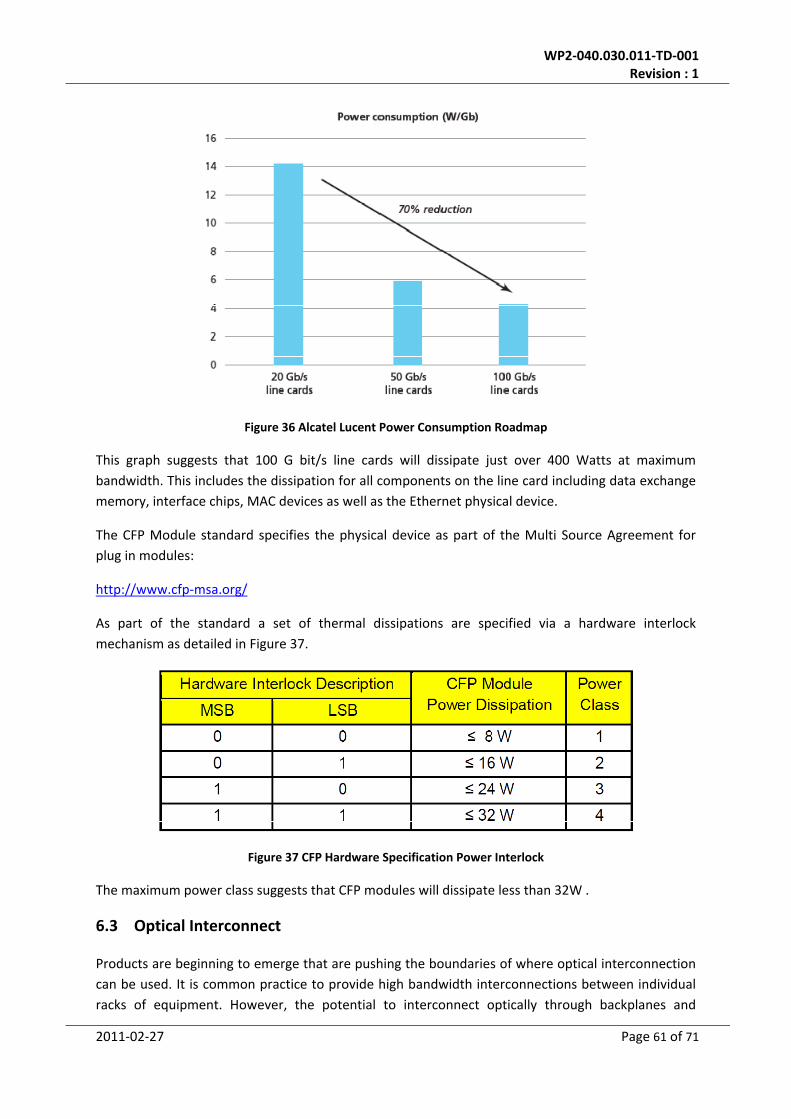
WP2‐040.030.011‐TD‐001 Revision : 1
2011‐02‐27 Page 61 of 71
Figure 36 Alcatel Lucent Power Consumption Roadmap
This graph suggests that 100 G bit/s line cards will dissipate just over 400 Watts at maximum
bandwidth. This includes the dissipation for all components on the line card including data exchange
memory, interface chips, MAC devices as well as the Ethernet physical device.
The CFP Module standard specifies the physical device as part of the Multi Source Agreement for
plug in modules:
http://www.cfp‐msa.org/
As part of the standard a set of thermal dissipations are specified via a hardware interlock
mechanism as detailed in Figure 37.
Figure 37 CFP Hardware Specification Power Interlock
The maximum power class suggests that CFP modules will dissipate less than 32W .
6.3 Optical Interconnect
Products are beginning to emerge that are pushing the boundaries of where optical interconnection
can be used. It is common practice to provide high bandwidth interconnections between individual
racks of equipment. However, the potential to interconnect optically through backplanes and

WP2‐040.030.011‐TD‐001 Revision : 1
2011‐02‐27 Page 62 of 71
eventually to individual chips is becoming a reality through the use of optical wave guides and lens
arrays. The provision of optical interconnectivity helps mitigate the traditional problems of thermal
dissipation and signal integrity issues associate with electrical connectivity.
The most prominent coverage of optical connection development in recent electronics press and
journals is IBMs development of the Terra Bus. For this reason this document focuses on IBM
technology to provide an over view.
The provisional time line suggested by IBM for the introduction of the technology is:
Today: rack to rack conventional optical modules and edge of card packaging
2011: Dense parallel fibre coupled modules close to the CPU
2015: Integrated transceivers and optical printed circuit boards
2020: 3‐D stack processing chips with transceivers integrated into processors.
http://www03.ibm.com/procurement/proweb.nsf/objectdocswebview/filepcb+‐
+ibm+opcb+roadmap+and+technology+‐+jeff+kash.pdf/$file/ibm+opcb+roadmap+and+tech+‐
+jeff+kash.pdf
IBM has already created a prototype printed circuit board that interconnects two modules using a
polymer waveguide. The overall concept is illustrated in Figure 38
Figure 38 IBM Terra Bus Overview
The modules a waveguide lens array that provides a mechanism for interfacing the optical signal in
and out of the waveguide. Detail of the optical lens array implementation in relation to the overall
module and printed circuit board is shown in Figure 39 and Figure 40 respectively.

WP2‐040.030.011‐TD‐001 Revision : 1
2011‐02‐27 Page 63 of 71
Figure 39 IBM Terrabus Integrated Circuit Connectivity
Figure 40 IBM Terrabus Integrated Circuit and Printed Circuit board Optical Connectivity
Within the module vertical‐cavity surface –emitting laser, VCSEL optical transmitters and photo
detector devices provide the optical transmit and receive capability respectively. It has been found
that at 850 nm wavelength there is less loss in the polymer waveguide and will currently support
communication over links of up to 1 metre. Industry is already producing VCSEL devices at 850nm in
high volume including multi‐channel devices. Emcore have 12 channel devices on their web‐site
http://www.emcore.com/fiber_optics/transceivers/12_channel_parallel that offer up to 5 G bps per
lane and 24 channels. IBM is using a special 24 channel variant of this device with 15 G bit/s
capability per lane.
As illustrated in Figure 39, a silicon carrier chip is used to host the components of the module.
Currently, IBM’s terrabus is using a carrier with dimensions of 10.4 x 6,4 mm. The laser & photo
diode arrays plus CMOS Tx and Rx components are soldered to carrier.
6.3.1 Performance
Current performance demonstrated by IBM at the SC07 show was 10 Gb/s along a 150mm bus
through utilising 32 way links operating at 985 nm. However, subsequent research has shown that
850 nm wavelengths are more optimal for transmitting through the waveguides and that data rates
of 360 Gb/s for up to 1 metre have been achieved. The current bandwidth density is 9 G b/s/mm2 .

WP2‐040.030.011‐TD‐001 Revision : 1
2011‐02‐27 Page 64 of 71
6.3.2 Thermal Dissipation
The current thermal dissipation for 24 channels each operating at 15 G bits/s bidirectional rate of
360 G b/s is 2.3 W. This equates to a power efficiency of 6.5 pJ per link
6.3.3 Cost
There are currently no cost estimates available.
7 Appendix 1
7.1 Moore’s Law
According to Wikipedia Moore’s law is based on Gordon Moore’s paper of 1965 that noted that
number of components in integrated circuits had doubled every year from the invention of the
integrated circuit in 1958 until 1965 and predicted that the trend would continue "for at least ten
years". His prediction has proved to be uncannily accurate, in part because the law is now used in
the semiconductor industry to guide long‐term planning and to set targets for research and
development. In general it is accepted that Moore’s Law is an observation that the number of
transistors within a device doubles every 18 months (see Figure 41) with current (2011) high end
devices having hundreds of millions of transistors.
Steve Timberger Xilinx
Figure 41 Numbers of Transistors for Intel Processors
The ability to include more transistors per chip has the bonus that the cost per transistor is also
exponentially decreasing as detailed in the ITRS roadmap (Figure 42)

WP2‐040.030.011‐TD‐001 Revision : 1
2011‐02‐27 Page 65 of 71
Figure 42 ITRS transistor cost predictions
Several parameters are closely linked to Moore’s law and the number of transistors per device and
are presented in Table 10
Parameter Current Value Yearly Factor Years to Double (Half)
Moore’s Law (grids on a die)** 1B 1.49 1.75
Gate Delay 150ps 0.87 (5)
Capability (grids / gate delay) 1.71 1.3
Device‐length wire delay 1.00
Die‐length wire delay / gate
delay
1.71 1.3
Pins per package 750 1.11 7
Aggregate off‐chip bandwidth 1.28 3
From Digital Systems Engineering, Dally and Poulton, 1998
** Ignores multi‐layer metal, 8‐layers in 2001
Table 10 Semiconductor parameter growth
This table shows that the number of transistors per device doubling every 18 months isn’t the full
story and that there are some parameters that are growing considerably slower rate such as pins per
package which takes 7 years to double and gate delay which takes 5 years to half.

WP2‐040.030.011‐TD‐001 Revision : 1
2011‐02‐27 Page 66 of 71
7.2 Transistor Size
The ability to increase the number of transistors on a device relies on the ability to reduce transistor
size and the ability to increase silicon area. A historical roadmap including projections to beyond
2020 are shown in Figure 43 which speculates on the existence of 4nm feature size at the extreme
end of the projection
Michael Keating SNUG 2010
Figure 43 Roadmap of Transistor Size
Taking a scaling factor of α for the feature size shrinkage, the behaviour of other aspects of the device can be derived and are shown in Table 11. How these parameters relate to the physical implementation of the device are illustrated in
Scaling Results
Voltage V/α Higher Density α2
Oxide tox/α Higher Speed α
Wire Width W/α Power/ ckt 1/α2
Gate Width L/α Power Density Constant
Diffusion Xd/α
Substrate Α * NA
Table 11 Device Scaling factors
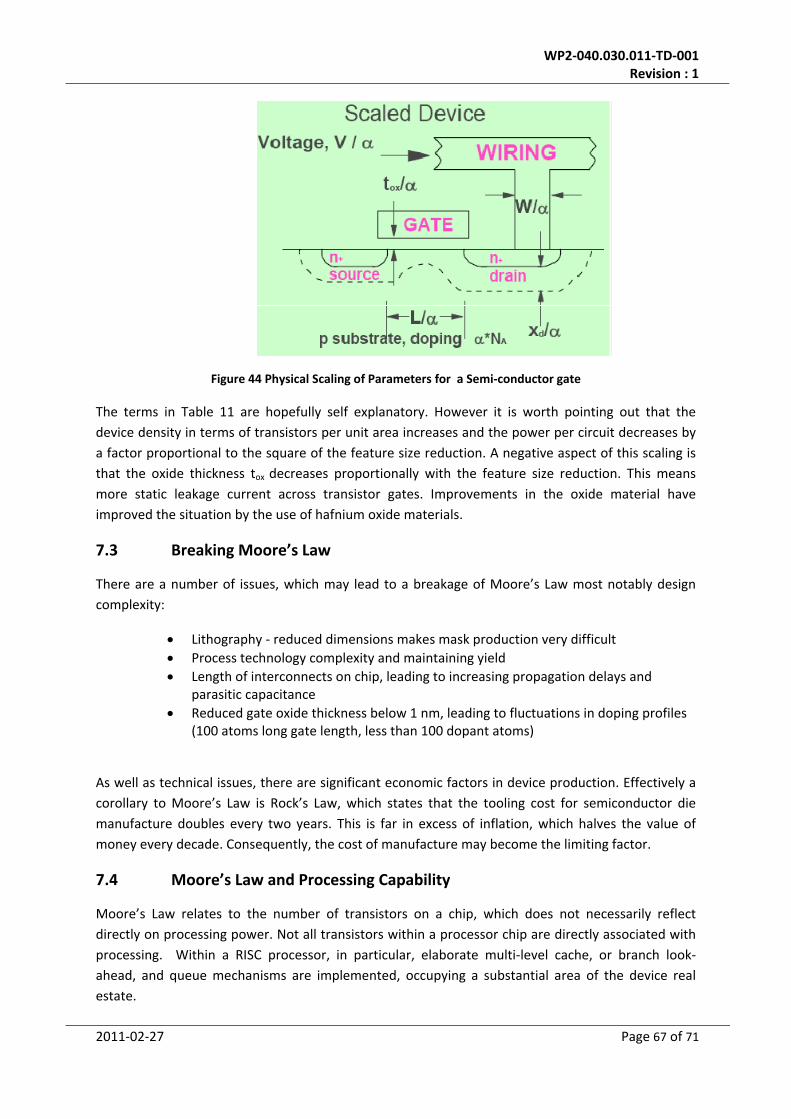
WP2‐040.030.011‐TD‐001 Revision : 1
2011‐02‐27 Page 67 of 71
Figure 44 Physical Scaling of Parameters for a Semi‐conductor gate
The terms in Table 11 are hopefully self explanatory. However it is worth pointing out that the
device density in terms of transistors per unit area increases and the power per circuit decreases by
a factor proportional to the square of the feature size reduction. A negative aspect of this scaling is
that the oxide thickness tox decreases proportionally with the feature size reduction. This means
more static leakage current across transistor gates. Improvements in the oxide material have
improved the situation by the use of hafnium oxide materials.
7.3 Breaking Moore’s Law
There are a number of issues, which may lead to a breakage of Moore’s Law most notably design
complexity:
Lithography ‐ reduced dimensions makes mask production very difficult
Process technology complexity and maintaining yield
Length of interconnects on chip, leading to increasing propagation delays and parasitic capacitance
Reduced gate oxide thickness below 1 nm, leading to fluctuations in doping profiles (100 atoms long gate length, less than 100 dopant atoms)
As well as technical issues, there are significant economic factors in device production. Effectively a
corollary to Moore’s Law is Rock’s Law, which states that the tooling cost for semiconductor die
manufacture doubles every two years. This is far in excess of inflation, which halves the value of
money every decade. Consequently, the cost of manufacture may become the limiting factor.
7.4 Moore’s Law and Processing Capability
Moore’s Law relates to the number of transistors on a chip, which does not necessarily reflect
directly on processing power. Not all transistors within a processor chip are directly associated with
processing. Within a RISC processor, in particular, elaborate multi‐level cache, or branch look‐
ahead, and queue mechanisms are implemented, occupying a substantial area of the device real
estate.

WP2‐040.030.011‐TD‐001 Revision : 1
2011‐02‐27 Page 68 of 71
Prior to the advent of the RISC processor in 1985, processing performance grew at a rate of 135%
per year. Subsequent processing performance growth has been averaging 160% per year. However,
this growth has been at the expense of ever‐increasing inefficiencies in the use of the silicon area
(and larger number of external connections).
As illustrated earlier, the dissipation expected from future processors increases exponentially with
respect to time. Reductions in operating voltage only slow the rate of increased dissipation by the
order of 30%. It should be noted, in passing, that the dissipation of a processor varies with
application it is running, depending on how many, and at what rate, transistors are being switched
by that application.
A summary of historic scaling factors:
Transistor count per chip has doubled every 18 months for over 40 years
Feature size has reduced by 30% every 2 to 3 years
Until recently speed increased by 30% per year
Function cost has reduced by ~ 25 to 30 % per year
Scaling is expected to continue until transistor gate lengths are ~ 10nm
Issues that may limit scaling:
Sub‐threshold current (off‐current) doesn’t scale
Electron tunnelling increases with small dimensions
Doping variations cause large threshold voltage variations
Power density as a result of leakage current increases more rapidly than dynamic power
8 Appendix 2
This appendix identifies other potentially interesting boutique technologies. Documentation on
these is kept at a minimum on purpose. On the whole, these technologies are higher risk as, at
present, they don’t necessarily represent the mainstream and on the whole will not be second
sourced .
8.1 Tilera
Tilera are a Californian based company with representation in China Japan and Korea that are
producing a processing chip with 16 to 100 identical processor cores (tiles) interconnected with an
on on‐chip network. Each tile consists of a processor with L1 and L2 cache plus a non‐blocking
switch that connects the tiles into the mesh. Each tile can independently run a full operating system,
or a group of multiple tiles can run a multi‐processing OS, like SMP Linux. This architecture is now in
its third generation with the TILE‐Gx family offering 100, 64, 36, and 16‐core versions as detailed in
Figure 45.

WP2‐040.030.011‐TD‐001 Revision : 1
2011‐02‐27 Page 69 of 71
Figure 45 Tilera Tile Processor architecture
The initial market for the Tile architecture was aimed at modelling climate conditions. However the
company are targeting the following sectors:
Cloud Computing
Networking
Wireless Infrastructure
Digital Media
(http://www.tilera.com/sites/default/files/productbriefs/PB025_TILE‐Gx_Processor_A_v3.pdf) :
8.2 Clearspeed
Clearspeed are a company in Oxon UK that currently have a low power processor containing 96
processing elements implemented in their CSX700 chip Figure 46. Further details are available at
http://www.clearspeed.com/
The main performance characteristics of the chip include:
250MHz core clock frequency
96 GFLOPS single or double precision
75 GFLOPS sustained double precision DGEMM
48 GMAC/s integer performance
9W typical power dissipation

WP2‐040.030.011‐TD‐001 Revision : 1
2011‐02‐27 Page 70 of 71
192 Gbytes/s internal memory bandwidth
2 x 4 Gbytes/s external memory bandwidth
4 Gbytes/s chip‐to‐chip bandwidth
Figure 46 Clearspeed’s CSX 700
Clearspeed’s have shown interest in the SKA project and have indicated that their technology will be
available as IP.
8.3 PicoChip
Picochip are a company from Cambridge that are producing processing chips targeting
telecommunication base stations.
http://www.picochip.com/
They have a low power low cost DSP solution based on multiple 16 bit Harvard Architecture
processing cores implemented in an architecture known as known as the Pico Array which is
illustrated in Figure 47. The claimed cost/performance ratio is below $1/GMAC in volume.
The processor cores include hardware acceleration for FFT and IFFT capability for up to 1024 points.
Picochip claim:
“Like an FPGA, the picoArray structure is defined at design‐time (not run‐time); tasks are
distributed “physically” in space; and deterministic, cycle‐accurate simulations are possible.
But, unlike an FPGA, timing closure is not an issue; design and build time is measured in
minutes and seconds, not hours; development is in C or assembler; and task granularity is at

WP2‐040.030.011‐TD‐001 Revision : 1
2011‐02‐27 Page 71 of 71
the word (or sample) level, so implementation is more efficient and programming is
inherently easier.”
Figure 47 PicoChip’s Pico Array Architecture.
8.4 Other Technologies
This section provides hyper‐links to other processing technologies that are of interest but not
necessarily directly applicable to the SKA. For example, the Netronome network processor is
designed for streamed processing using 40 processor cores and support for 10 G bit Ethernet
interface but is designed for deep packet inspection rather than signal processing.
Cavium: real time Deep Packet Inspection processing technology
http://www.caviumnetworks.com/newsevents_Caviumnetworks_Heavy‐Reading‐
Report.html
Aspex Semiconductor: Real time video encoding DSP technology
http://www.aspex‐semi.com/
Freescale:
http://www.freescale.com/
Storm Stream processor
http://www.streamprocessors.com/
Netronome Network Processor:
http://www.netronome.com/