techshanghai2016 - rf front-end module roadmap and handset architecture challenges in future mmwave...
TRANSCRIPT

RF Front-End Module Roadmap and Handset Architecture Challenges in Future mmWave Technology
Anirban BandyopadhyayDirector, Strategic Applications
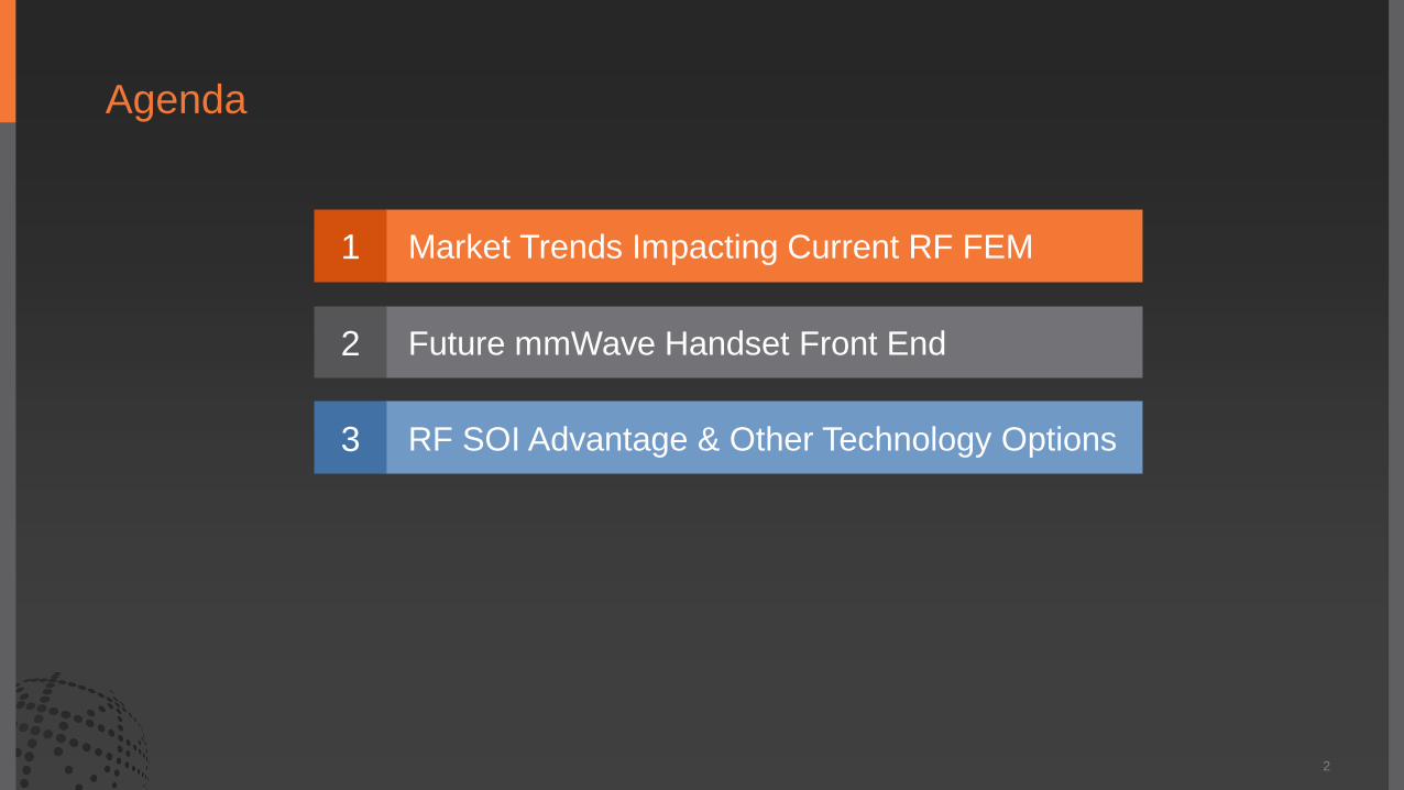
Agenda
2
Market Trends Impacting Current RF FEM
Future mmWave Handset Front End
RF SOI Advantage & Other Technology Options
1
2
3

Agenda
3
Market Trends Impacting Current RF FEM
Future mmWave Handset Front End
RF SOI Advantage & Other Technology Options
1
2
3

Access to high-speed data through LTE driving smartphone growth
• Low latency:
– Improved user experience
• High peak data rates:
– Rich content delivery (HD, 4K video)
• Scalable capacity/bandwidth:
– Efficient network deployment
• Spectrally efficient:
– Improved spectrum reuse
4
Source: IHS Smartphone Electronics Design Intelligence Database - Q2 2015
0
500
1000
1500
2000
2500
2014 2015 2016 2017 2018 2019
Mill
ions o
f U
nits
Handset Shipments
2/2.5G 3G LTE
Overall growth: 3.9% CAGR (2014-2019)LTE growth: 26.2% CAGR

Cellular Standards Roadmap
5
There’s a plan for < 6GHz version of 5G before 2020, not mentioned here
2010 ~2020 2030
LTE LTE Advanced
mmWave 5G(> 24 GHz)
Further backward compatible enhancements
Carrier Aggregation, Unlicensed bands
MTC256 QAM
6
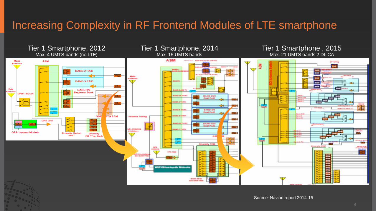
Tier 1 Smartphone , 2015Max. 21 UMTS bands 2 DL CA
Tier 1 Smartphone, 2014 Max. 15 UMTS bands
Tier 1 Smartphone, 2012 Max. 4 UMTS bands (no LTE)
Source: Navian report 2014-15
Increasing Complexity in RF Frontend Modules of LTE smartphone
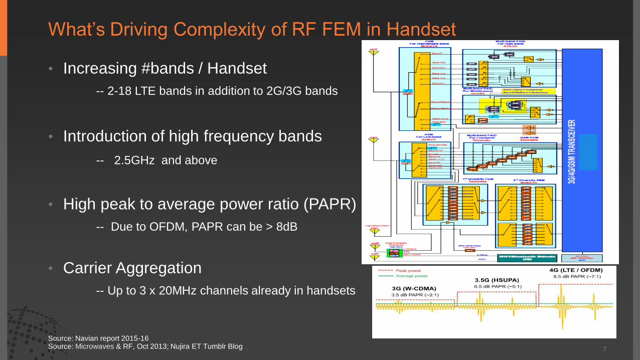
What’s Driving Complexity of RF FEM in Handset
7
• Increasing #bands / Handset
-- 2-18 LTE bands in addition to 2G/3G bands
• Introduction of high frequency bands
-- 2.5GHz and above
• High peak to average power ratio (PAPR)
-- Due to OFDM, PAPR can be > 8dB
• Carrier Aggregation
-- Up to 3 x 20MHz channels already in handsets
Source: Navian report 2015-16Source: Microwaves & RF, Oct 2013; Nujira ET Tumblr Blog
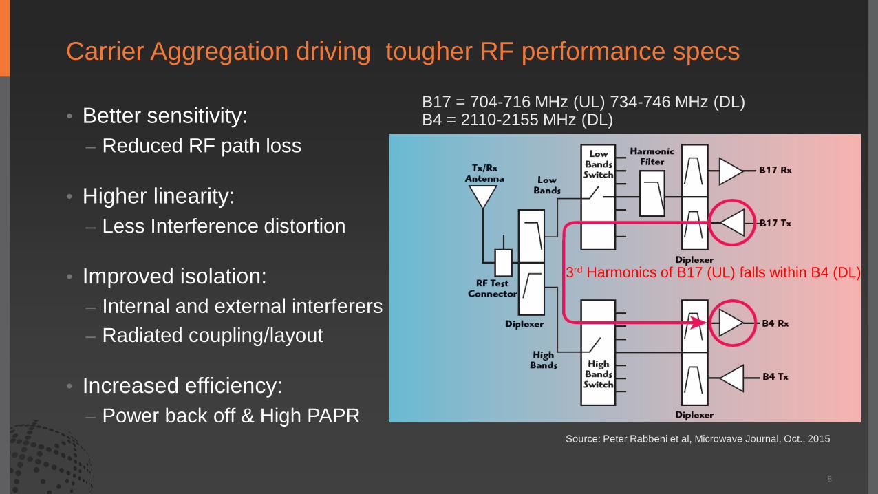
Carrier Aggregation driving tougher RF performance specs
• Better sensitivity:
– Reduced RF path loss
• Higher linearity:
– Less Interference distortion
• Improved isolation:
– Internal and external interferers
– Radiated coupling/layout
• Increased efficiency:
– Power back off & High PAPR
8
Source: Peter Rabbeni et al, Microwave Journal, Oct., 2015
B17 = 704-716 MHz (UL) 734-746 MHz (DL)B4 = 2110-2155 MHz (DL)
3rd Harmonics of B17 (UL) falls within B4 (DL)

50
60
70
80
90
100
2012 2014 2016 2018 2020
IIP
3, d
Bm
LTE-A standard driving challenging requirements for linearity
• FDD LTE/LTE-A requires co-existence of transmit/receive
• Creates challenges for TX/RX isolation and interferers due to CA band pairs (DL CA today; UL CA in future)
• TD-LTE could help mitigate or reduce these requirements in the future
9
Source: Intel Mobile Corporation, “Challenges for Radios Due to Carrier Aggregation Requirements,” by Larry Schumacher, Nov. 6, 2012
4G LTE-A
4G LTE
3G
2G

RF FEM Technology Trends – Module level Integration
10
PA
AntennaTuners
PowerAmplifiers
Antenna/Mode Switches
Filters, Duplexers
LNA, LNA+Switch
2010 2012 2014 2016 2018 2020
GaAs
RF SOI
GaAs
RF SOI
RF SOI
RF MEMS?
RF MEMS?
SAW
BAW
GaAs
RF SOI
Source: Jerome Azemar, Yole, Saxony SOI Forum - July, 2015; GLOBALFOUNDRIES marketing insight
SiGeCMOSSi LDMOS

RF SOI – the dominant Semiconductor technology for RF Front End
• Device stacking:
– Helps in addressing high p-p voltage swing across RF Switches
• Substrate benefits for RF:
– Reduced parasitics higher Q and lower loss
– Increased isolation/linearity
• Logic and control integration:
– MIPI interface now standard
• Low cost:
– Better economics than III-V
• Mainstream silicon manufacturing:
– Readily available capacity, migration to 300mm capacity, die cost
11
Source: FDSOI and RFSOI Forum - February 27, 2015

RxDiversity
RxDiversity Switch
AntennaTuner
Diplexer
Rx LowBand
Rx HighBand
MIPI
Tx HighBand
TxLow Band
PowerAmplifier
PA ModeSwitch
FilterBank
AntennaSwitch Module
AntennaSwap Switch
Coupler
MODEM
+
TRANSCEIVER
3GLTE
2G
2G
3GLTE
SupplyModulator
How to reduce component count ….Tunability?
• Significant work continues around the concept of introducing tunability into the FEM architecture
• Many different approaches have been investigated
– Hybrid – electrical tuning w/ acoustics
– Electrically tunable notch filters on SOI
– N-path Filters
• Requirements for low loss, high out of band rejection and reasonable percentage bandwidth are difficult to achieve simultaneously
12
Latest generation: 12 duplexers and 37 band pass filters!!!
Source: SOITEC White Paper, Nov. 2013
Agenda
13
Market Trends Impacting Current RF FEM
Future mmWave Handset Front End
RF SOI Advantage & Other Technology Options
1
2
3

Why mmWave 5G?
• Higher channel Bandwidth & data rate ( > 10 Gb/s)
•
• High Antenna efficiency (smaller size, higher gain)
• Higher spectral efficiency ( massive MIMO, spatial multiplexing for multi users)
• Interference Mitigation (narrow antenna beam, beam steering)
• Better cell edge coverage (small cells, directed beam)
14
Possible frequency band allocations within 24-33GHz, 37-50 GHz, 66-76GHz, 81-86 GHz
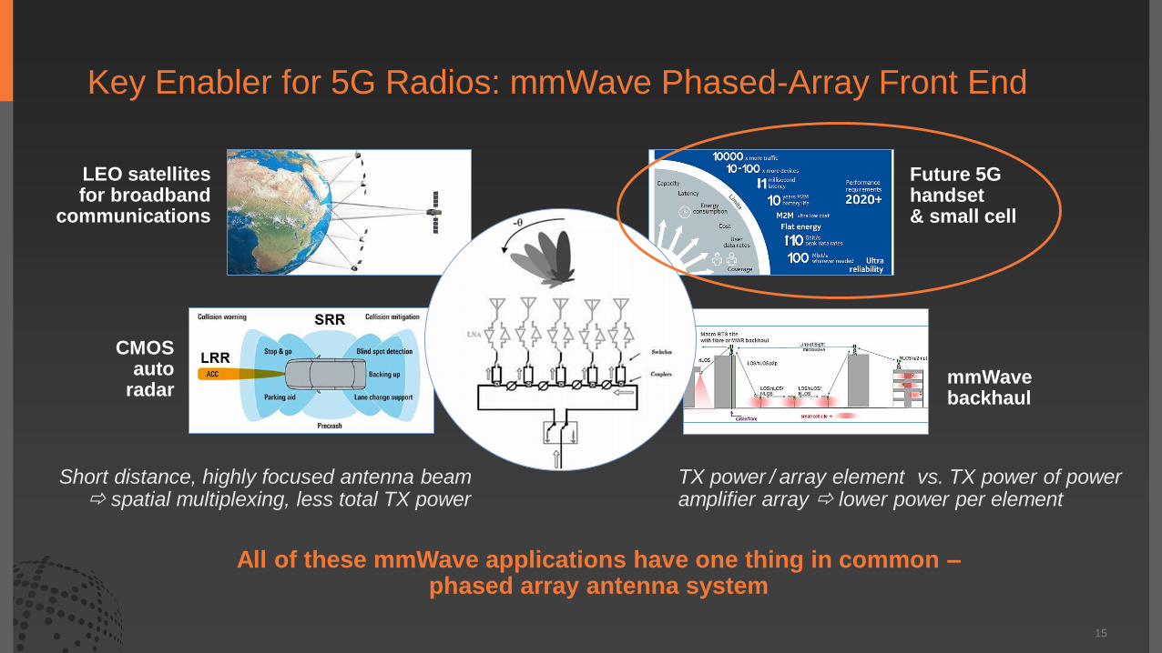
Key Enabler for 5G Radios: mmWave Phased-Array Front End
15
All of these mmWave applications have one thing in common –phased array antenna system
LEO satellites for broadband
communications
Future 5G handset & small cell
mmWave backhaul
TX power / array element vs. TX power of power amplifier array lower power per element
Short distance, highly focused antenna beam spatial multiplexing, less total TX power
CMOS auto
radar
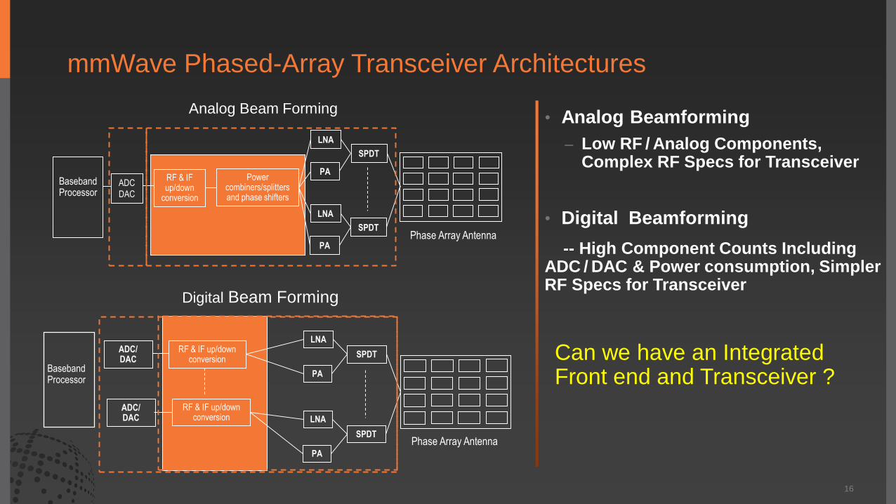
mmWave Phased-Array Transceiver Architectures
16
RF & IF up/down conversion
LNA
PA
SPDT
LNA
PA
SPDT
RF & IF up/down conversion
ADC/DAC
ADC/DAC
Digital Beam Forming
Baseband Processor
Phase Array Antenna
Baseband Processor
RF & IF up/down
conversion
LNA
PA
SPDT
LNA
PA
SPDT
Power combiners/splitters and phase shifters
Analog Beam Forming
ADC
DAC
Phase Array Antenna
• Analog Beamforming
– Low RF / Analog Components, Complex RF Specs for Transceiver
• Digital Beamforming
-- High Component Counts Including ADC / DAC & Power consumption, Simpler RF Specs for Transceiver
Can we have an Integrated Front end and Transceiver ?
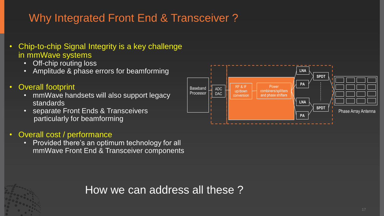
Why Integrated Front End & Transceiver ?
17
• Chip-to-chip Signal Integrity is a key challenge in mmWave systems
• Off-chip routing loss• Amplitude & phase errors for beamforming
• Overall footprint • mmWave handsets will also support legacy
standards• separate Front Ends & Transceivers
particularly for beamforming
• Overall cost / performance• Provided there’s an optimum technology for all
mmWave Front End & Transceiver components
How we can address all these ?
Baseband Processor
RF & IF up/down
conversion
LNA
PA
SPDT
LNA
PA
SPDT
Power combiners/splitters and phase shifters
ADC
DAC
Phase Array Antenna

Essential Elements for a mmWave Technology
18
• High f T / f MAX (3-5X operating frequency)
• Cu backend, stack height, substrate resistivity
Good RF model-to-hardware correlation
• DRC / LVS / PEX
High performance technology
Low loss BEOL
Well-modeled
technology
Design enablement
Scalable transmission
line & mmWave passives
• Validated mmWave design library to minimize EM simulation
Advanced bulk CMOS technologies provide high Ft/Fmax but BEOL stack scaling deteriorates passive loss and BEOL parasitics
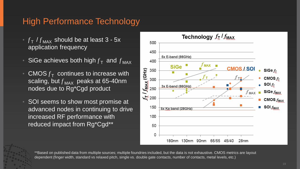
High Performance Technology
• f T / f MAX should be at least 3 - 5x
application frequency
• SiGe achieves both high f T and f MAX
• CMOS f T continues to increase with
scaling, but f MAX peaks at 65-40nm
nodes due to Rg*Cgd product
• SOI seems to show most promise at
advanced nodes in continuing to drive
increased RF performance with
reduced impact from Rg*Cgd**
19
**Based on published data from multiple sources; multiple foundries included, but the data is not exhaustive. CMOS metrics are layout
dependent (finger width, standard vs relaxed pitch, single vs. double gate contacts, number of contacts, metal levels, etc.)

Low Loss BEOL
Wavelength at 60GHz in SiO2 = 2.4mm; at 30GHz = 4.8mm
• Long transmission lines not uncommon
• Minimizing loss in BEOL is important
Availability of thick Cu levels and distance to ground plans are key to minimizing losses in BEOL
• Distance to ground plane may be difficult to achieve in advanced nodes
• Substrate resistivity
• SiGe: typically best of breed with tall vias and thick Cu and Al levels
• CMOS: RF additions with thick Cu levels
• Example for 90nm SiGe BiCMOS (courtesy of Professor Gabriel Rebeiz, UCSD)
– Lower loss (0.25 dB/mm) with increased distance to ground plane
20
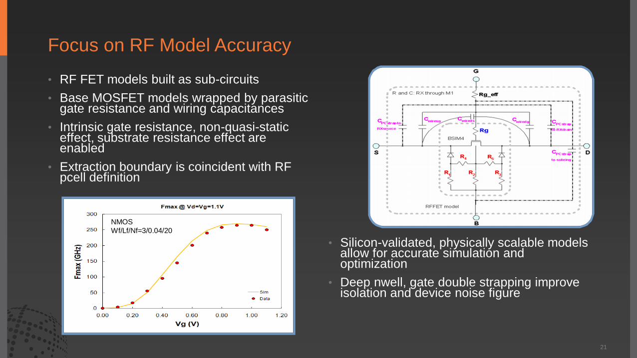
Focus on RF Model Accuracy
• RF FET models built as sub-circuits
• Base MOSFET models wrapped by parasitic gate resistance and wiring capacitances
• Intrinsic gate resistance, non-quasi-static effect, substrate resistance effect are enabled
• Extraction boundary is coincident with RF pcell definition
• Silicon-validated, physically scalable models allow for accurate simulation and optimization
• Deep nwell, gate double strapping improve isolation and device noise figure
21
NMOS
Wf/Lf/Nf=3/0.04/20
Agenda
22
Market Trends Impacting Current RF FEM
Future mmWave Handset Front End
RF SOI Advantage & Other Technology Options
1
2
3

Is there a technology w/ both High Ft/ Fmax & low BEOL loss at mmWave frequencies ?
45nm SOI – server technology , but has been extensively evaluated for mmWave building blocks:
• Measured peak f T is 264GHz for a 30 X 1007nm single-gate contact, relaxed-pitch transistor
• Best f MAX of 283GHz is achieved by a 58 X 513nm single-gate contact regular pitch transistor
23
Source: O. Inac, M. Uzunkol and G. Rebeiz, “45-nm CMOS SOI Technology Characterization for Millimeter-Wave Applications”
Measured f MAX of 30-µm transistors with different gate finger widths. Measured f T of relaxed pitch transistors.
24
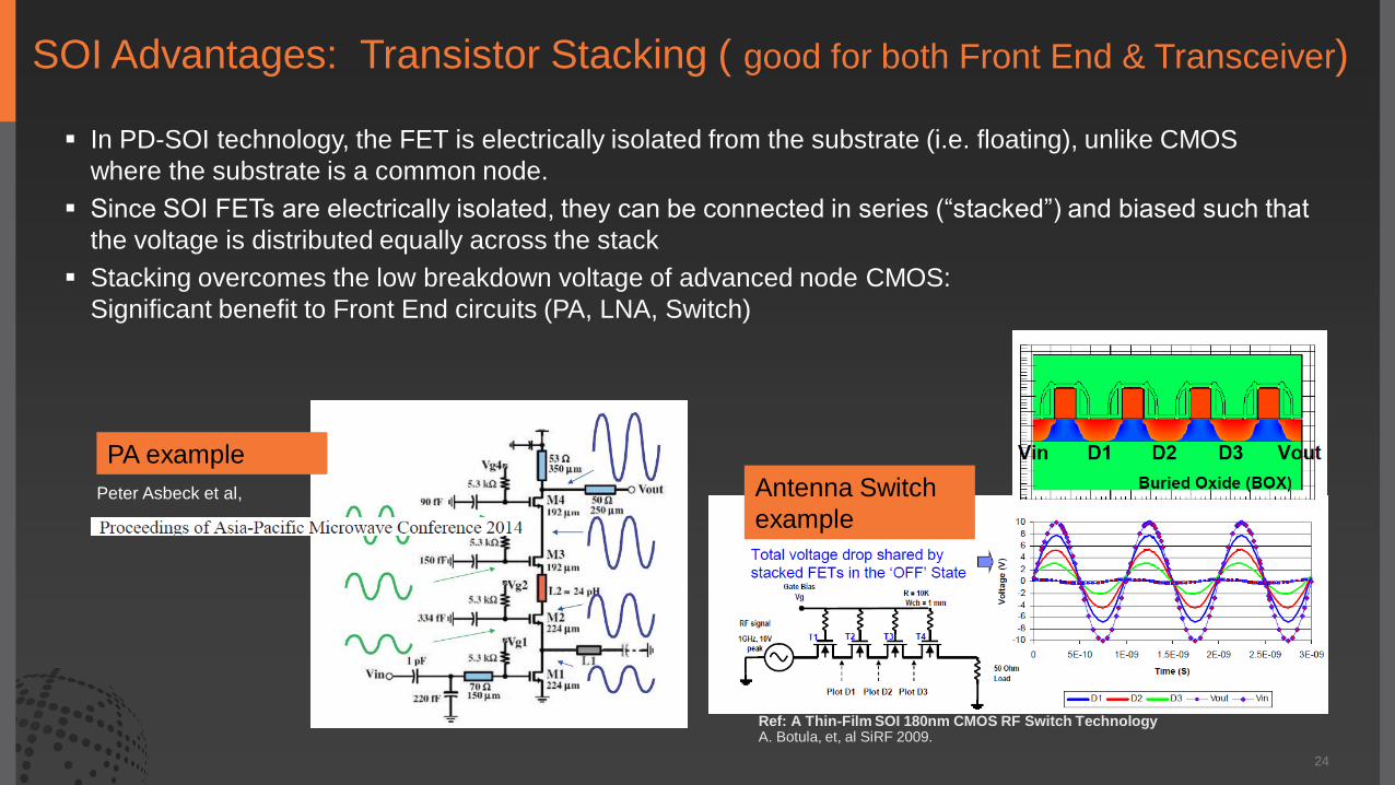
SOI Advantages: Transistor Stacking ( good for both Front End & Transceiver)
In PD-SOI technology, the FET is electrically isolated from the substrate (i.e. floating), unlike CMOS
where the substrate is a common node.
Since SOI FETs are electrically isolated, they can be connected in series (“stacked”) and biased such that
the voltage is distributed equally across the stack
Stacking overcomes the low breakdown voltage of advanced node CMOS:
Significant benefit to Front End circuits (PA, LNA, Switch)
Antenna Switch
example
PA example
Peter Asbeck et al,
Ref: A Thin-Film SOI 180nm CMOS RF Switch TechnologyA. Botula, et, al SiRF 2009.

RF SOI mmWave Power Amplifier Design
SOI enables transistor stacking for superior RF PA:
• Stacked configuration has higher power-added efficiency & smaller chip area vs. bulk CMOS:
– Buried-oxide layer electrically isolates transistors, mitigating substrate leakage / breakdown
– Configuration has higher input and output impedances for matching networks with lower loss & higher bandwidth
• Parasitic capacitances to substrate are significantly reduced, minimizing phase & voltage swing imbalance
25
Source Frequency range PAE Saturated output power
1 27 to 39GHz 33% @ 32GHz 22.4 dBm
2 25 to 35GHz 29% @ 29GHz 24.5 dBm
3 42 to 45GHz 34% @ 42.5 GHz 19.4 dBm
4 42 to 54GHz 42% @ 46GHz 22.4 dBm
1. “Millimeter-Wave Power Amplifiers in 45nm CMOS SOI Technology”, Jing-Hwa Chen, Sultan R. Helmi and Saeed Mohammadi
2. “28GHz >250mW CMOS Power Amplifier Using Multigate-Cell Design, Jefy A. Jayamon, James F. Buckwalter and Peter M. Asbeck, CICS 2015
3. “A 34% PAE, 18.6dBm 42-45GHz Stacked Power Amplifier in 45nm SOI CMOS” Amir Agah, Hayg Dabag, Bassel Hanafi, Peter Asbeck, Lawrence Larson and James Buckwalter
4. “High-Efficiency Microwave and mm-Wave Stacked Cell CMOS SOI Power Amplifiers”, Sutlan R. Helmi, Jing-Hwa Chen and Saeed Mohammadi, TMM 2015
Source: “A Broadband Stacked Power Amplifier in 45-nm CMOS SOI Technology”, Jing-Hwa Chen, Sultan R. Helmi, Reza Azedegan, Farshid Aryanfar and Saeed Mohammadi.
Published results (45nm SOI):

RF SOI mmWave RF Switch Design
RF SOI enables transistor stacking for superior RF switch performance:
• Buried-oxide layer electrically isolates transistors, mitigating substrate leakage
• Junction capacitors are much smaller
• Linearity is enhanced
• Optimizing for insertion loss is simpler
• 3-4 stack 45nm RFSOI switches are sufficient to meet the 24dBm power level with 25dBm isolation
26
1. Source: M. Parlak, J.F. Buckwalter,“A 2.5-dB Insertion Loss, DC-60 GHz CMOS SPDT Switch in 45-nm
SOI”CSICS 2011
Source: M. Parlak, J.F. Buckwalter,“A 2.5-dB Insertion Loss, DC-60 GHz
CMOS SPDT Switch in 45-nm SOI”CSICS 2011
Source Frequency Insertion Loss Isolation IIP3
1 45GHz 1.7 dB >25 dB 18.2 dBm
Published results (45nm):

RF SOI mmWave LNA Design
SOI enables cascode approach for superior RF LNA:
• Lower NF in cascode architecture (not possible in bulk Si)
• Enhanced stability due to lower parasitic capacitance
• Buried-oxide layer electrically isolates substrate, reducing noise coupling
• Linearity is enhanced
27
Source: M. Parlak, J.F. Buckwalter,“A 2.5-dB Insertion Loss, DC-60 GHz
CMOS SPDT Switch in 45-nm SOI”CSICS 2011
Source: O. Inac, B. Cetinoneri, M. Uzunkol, Y. A. Atesal and G. M. Rebeiz, “Millimeter-Wave and
THz Circuits in 45-nm SOI CMOS”
Published results (45nm):
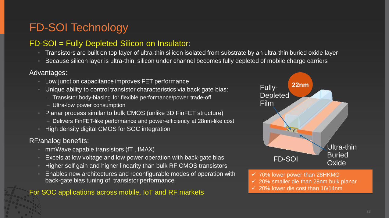
FD-SOI Technology
FD-SOI = Fully Depleted Silicon on Insulator:• Transistors are built on top layer of ultra-thin silicon isolated from substrate by an ultra-thin buried oxide layer
• Because silicon layer is ultra-thin, silicon under channel becomes fully depleted of mobile charge carriers
Advantages:
• Low junction capacitance improves FET performance
• Unique ability to control transistor characteristics via back gate bias:
– Transistor body-biasing for flexible performance/power trade-off
– Ultra-low power consumption
• Planar process similar to bulk CMOS (unlike 3D FinFET structure)
– Delivers FinFET-like performance and power-efficiency at 28nm-like cost
• High density digital CMOS for SOC integration
RF/analog benefits:
• mmWave capable transistors (fT , fMAX)
• Excels at low voltage and low power operation with back-gate bias
• Higher self gain and higher linearity than bulk RF CMOS transistors
• Enables new architectures and reconfigurable modes of operation with back-gate bias tuning of transistor performance
For SOC applications across mobile, IoT and RF markets
28
Ultra-thin BuriedOxide
FD-SOI
Fully-DepletedFilm
22nm
70% lower power than 28HKMG
20% smaller die than 28nm bulk planar
20% lower die cost than 16/14nm

FD-SOI Body-Biasing Enables Power/Performance Trade-Off and Tuning of RF/Analog Parameters
29
Forward BB (FBB) enables low voltage operation without speed loss
Reverse BB (RBB) enables low leakage down to 1pA/micron
Dynamic body biasing enables tuning RF/Analog characteristics: gM, gDS, self-gain, fT, fMAX
Body biasing is an effective knob to tune RF performance characteristics
Max Frequency
LeakagePower
ReverseBody Bias(RBB)
ForwardBody Bias
(FBB)
Maximum PerformanceOperating Mode
Minimum LeakageIn Standby Mode
-2V to +2V
Body-Biasing
RF back gate bias reduces the Vt and extends the dynamic range
Peak fMAX: Vg ~ 0.75 - 0.8 V
Dyn.Range

Technology choices for mmWave Applications
30
Technology + - Comments
RF CMOS
(65nm - 28nm)
• Lowest wafer cost (w.r.t. same
lithography node)
• SOC integration with RF, ADC,
digital baseband, memory
• Platform IP availability
• Low breakdown voltage
• Low Tx output power /
efficiency at mmWave
• Low self gain
• Poor device isolation
• mmWave performance
decreases at 28nm
Best choice for price
sensitive lower
performance (short range)
applications.
PD-SOI
(65nm - 45nm)
• FEM + RF integration
• Device stacking with higher
voltage / power handling vs
• Great fT / fMAX,
• Rx Noise Figure
• High resistivity substrate
• SOI substrate cost adder
(vs same node CMOS)
• Lower logic density for SOC
integration than 28nm and
22nm
Good cost/performance
tradeoff.
FD-SOI
(28nm - 22nm)
• High self gain vs CMOS
• High fT / fMAX
• Lowest voltage / power
operation with back-gate bias
High density SOC integration
• Low mask count
• SOI substrate cost adder
• High NRE (most advanced
lithography)
• Device stacking more
complex and less effective
than PD-SOI
New capability in industry
with back-gate bias ->
potential for reconfigurable
operation
SiGe
(130nm - 90nm)
• Optimized for mmWave
• Best fT / fMAX, phase noise
• Best Tx output power and
efficiency per element
• Lowest loss metal stack
• Highest wafer cost/mm2
• Not suitable for SOC
integration with ADC,
baseband
Best choice for high
performance and high Tx
power (longer range)
mmWave applications
Oxide Insulator
Silicon
Silicon Wafer

Summary
• Evolution of LTE supporting increasing demand of data rate and driving greater RF system complexity and performance challenges
• The future mmWave based radio interface will have different architectures and technical challenges
• There are different Silicon Technology options for mmWave Handset Front End – but Advanced RFSOI is well suited to integrate Front End with Transceiver
• Even though the carrier frequencies and mmWave specs are still being decided, different Front End and Transceiver components have been demonstrated on RF SOI covering 28-94GHz for possible use in both handsets and small cells
31
Trademark Attribution
GLOBALFOUNDRIES®, the GLOBALFOUNDRIES logo and combinations thereof, and GLOBALFOUNDRIES’ other trademarks and service marks are owned by GLOBALFOUNDRIES Inc. in the United States and/or other jurisdictions. All other brand names, product names, or trademarks belong to their respective owners and are used herein solely to identify the products and/or services offered by those trademark owners.
© 2016 GLOBALFOUNDRIES Inc. All rights reserved.
Thank [email protected]