television and video engineering - tamilnadu sem 7/ec2034... · ec 2034 television and video...
TRANSCRIPT

A Course Material on
TELEVISION AND VIDEO ENGINEERING
By
Mr. B.RAJAGNANAPAZHAM
ASSISTANT PROFESSOR
DEPARTMENT OF ELECTRONICS AND COMMUNICATION ENGINEERING
SASURIE COLLEGE OF ENGINEERING VIJAYAMANGALAM – 638 056

SCE 2 ECE DEPARTMENT
EC 2034 TELEVISION AND VIDEO ENGINEERING
QUALITY CERTIFICATE
This is to certify that the e-course material
Subject Code : EC 2034
Subject : TELEVISION AND VIDEO ENGINEERING
Class : IV Year ECE
being prepared by me and it meets the knowledge requirement of the university curriculum.
Signature of the Author
Name: Mr.B. RAJAGNANAPAZHAM
Designation: Assistant Professor
This is to certify that the course material being prepared by Mr.B.RAJAGNANAPAZHAM is of adequatequality. He has referred more than five books among them minimum one is from abroad author.
Signature of HD
Name: Dr.K.PANDIARAJAN
SEAL

SCE 3 ECE DEPARTMENT
EC 2034 TELEVISION AND VIDEO ENGINEERING
EC2034 TELEVISION AND VIDEO ENGINEERING
UNIT I FUNDAMENTALS OF TELEVISION
Aspect ratio-Image continuity-Number of scanning lines-Interlaced scanning-Picture resolution-Cameratubes-Image Orthicon-Vidicon- Plumbicon- Silicon Diode Array Vidicon- Solid-state Image scanners-Monochrome picture tubes- Composite video signal- video signal dimension-horizontal sync. Composition-vertical sync. Details functions of vertical pulse train- Scanning sequence details. Picture signaltransmission positive and negative modulation- VSB transmission- Sound signal transmission- Standardchannel bandwidth.
UNIT II MONOCHROME TELEVISION TRANSMITTER AND RECEIVER
TV transmitter-TV signal Propagation- Interference- TV Transmission Antennas-Monochrome TVreceiver- RF tuner- UHF, VHF tuner-Digital tuning techniques-AFT- IF subsystems-AGC Noisecancellation-Video and Sound inter-carrier detection-Vision IF subsystem- DC re-insertion-Videoamplifier circuits-Sync operation- typical sync processing circuits-Deflection current waveforms,Deflection oscillators- Frame deflection circuits- requirements- Line deflection circuits-EHT generation-Receiver antennas.UNIT III ESSENTIALS OF COLOUR TELEVISION
Compatibility- Colour perception-Three colour theory- Luminance, Hue and saturation- Colour televisioncameras-Values of luminance and colour difference signals-Colour television display tubes-Delta-gunPrecision-in-line and Trinitron colour picture tubes- Purity and convergence- Purity and static and Dynamicconvergence adjustments- Pincushion-correction techniques-Automatic degaussing circuit- Gray scaletracking colour signal transmission- Bandwidth-Modulation of colour difference signals-Weighting factors-Formation of chrominance signal.
UNIT IV COLOUR TELEVISION SYSTEMS
NTSC colour TV systems-SECAM system- PAL colour TV systems- Cancellation of phase errors-PAL-DColour system-PAL coder-PAL-Decoder receiver-Chromo signal amplifier-separation of U and V signals-colour burst separation-Burst phase Discriminator-ACC amplifier-Reference Oscillator-Ident and colourkiller circuits-U and V demodulators- Colour signal matrixing. Sound in TV
UNIT V ADVANCED TELEVISION SYSTEMS
Satellite TV technology-Geo Stationary Satellites-Satellite Electronics-Domestic Broadcast System-CableTV-Cable Signal Sources-Cable Signal Processing, Distribution & Scrambling- Video Recording-VCRElectronics-Video Home Formats- Video Disc recording and playback-DVD Players-Tele Text Signalcoding and broadcast receiver- Digital television-Transmission and reception –Projection television-Flatpanel display TV receivers-LCD and Plasma screen receivers-3DTV-EDTV.TEXTBOOKS:1. R.R.Gulati, “Monochrome Television Practice, Principles, Technology and servicing.” Third Edition2006, New Age International (P) Publishers.2. R.R.Gulati, Monochrome & Color Television, New Age International Publisher, 2003.
REFERENCES:1. A.M Dhake, “Television and Video Engineering”, 2nd ed., TMH, 2003.2. R.P.Bali, Color Television, Theory and Practice, Tata McGraw-Hill, 1994
SCE 4 ECE DEPARTMENT
EC 2034 TELEVISION AND VIDEO ENGINEERING
EC 2034 TELEVISION AND VIDEO ENGINEERING
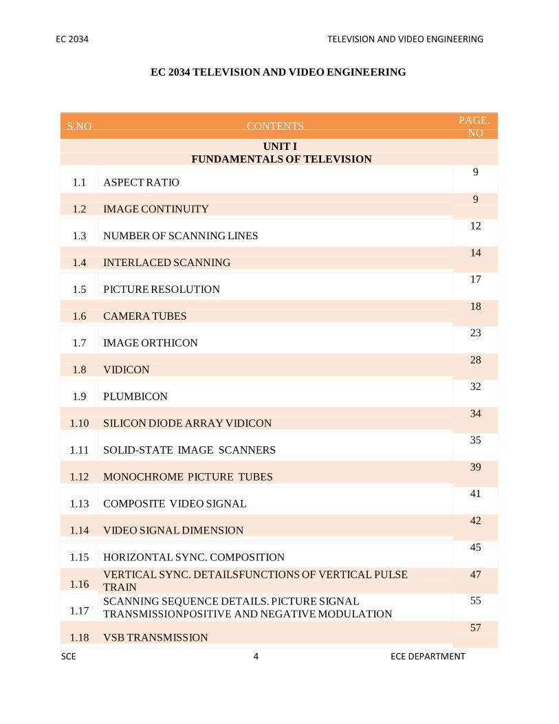
S.NO CONTENTS PAGE.NO
UNIT IFUNDAMENTALS OF TELEVISION
1.1 ASPECT RATIO9
1.2 IMAGE CONTINUITY9
1.3 NUMBER OF SCANNING LINES12
1.4 INTERLACED SCANNING14
1.5 PICTURE RESOLUTION17
1.6 CAMERA TUBES18
1.7 IMAGE ORTHICON23
1.8 VIDICON28
1.9 PLUMBICON32
1.10 SILICON DIODE ARRAY VIDICON34
1.11 SOLID-STATE IMAGE SCANNERS35
1.12 MONOCHROME PICTURE TUBES39
1.13 COMPOSITE VIDEO SIGNAL41
1.14 VIDEO SIGNAL DIMENSION42
1.15 HORIZONTAL SYNC. COMPOSITION45
1.16VERTICAL SYNC. DETAILSFUNCTIONS OF VERTICAL PULSETRAIN
47
1.17SCANNING SEQUENCE DETAILS. PICTURE SIGNALTRANSMISSIONPOSITIVE AND NEGATIVE MODULATION
55
1.18 VSB TRANSMISSION57
EC 2034 TELEVISION AND VIDEO ENGINEERING
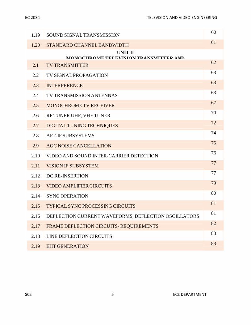
1.19 SOUND SIGNAL TRANSMISSION60
1.20 STANDARD CHANNEL BANDWIDTH61
UNIT IIMONOCHROME TELEVISION TRANSMITTER AND
2.1 TV TRANSMITTER62
2.2 TV SIGNAL PROPAGATION63
2.3 INTERFERENCE63
2.4 TV TRANSMISSION ANTENNAS63
2.5 MONOCHROME TV RECEIVER67
2.6 RF TUNER UHF, VHF TUNER70
2.7 DIGITAL TUNING TECHNIQUES72
2.8 AFT-IF SUBSYSTEMS74
2.9 AGC NOISE CANCELLATION75
2.10 VIDEO AND SOUND INTER-CARRIER DETECTION76
2.11 VISION IF SUBSYSTEM77
2.12 DC RE-INSERTION77
2.13 VIDEO AMPLIFIER CIRCUITS79
2.14 SYNC OPERATION80
2.15 TYPICAL SYNC PROCESSING CIRCUITS81
2.16 DEFLECTION CURRENT WAVEFORMS, DEFLECTION OSCILLATORS81
2.17 FRAME DEFLECTION CIRCUITS- REQUIREMENTS82
2.18 LINE DEFLECTION CIRCUITS83
2.19 EHT GENERATION83
SCE 5 ECE DEPARTMENT
EC 2034 TELEVISION AND VIDEO ENGINEERING
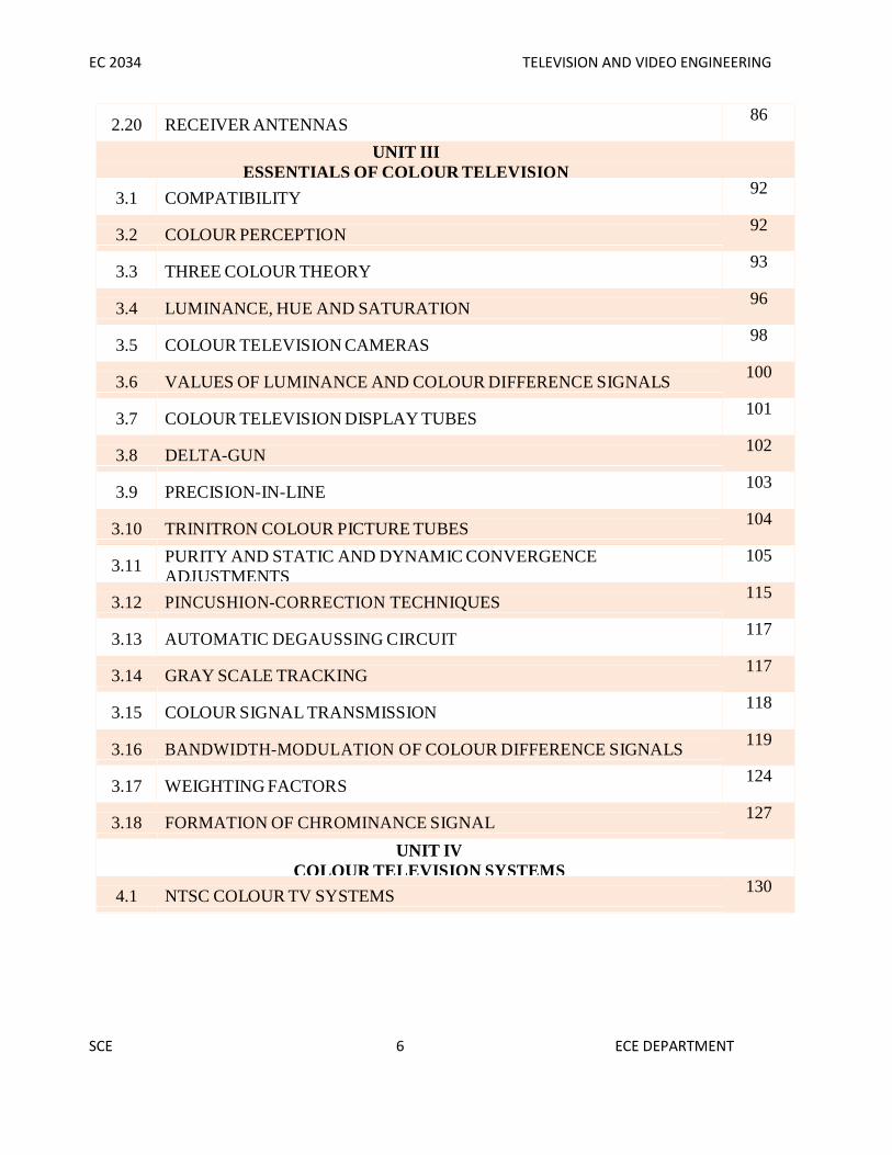
2.20 RECEIVER ANTENNAS86
UNIT IIIESSENTIALS OF COLOUR TELEVISION
3.1 COMPATIBILITY92
3.2 COLOUR PERCEPTION92
3.3 THREE COLOUR THEORY93
3.4 LUMINANCE, HUE AND SATURATION96
3.5 COLOUR TELEVISION CAMERAS98
3.6 VALUES OF LUMINANCE AND COLOUR DIFFERENCE SIGNALS100
3.7 COLOUR TELEVISION DISPLAY TUBES101
3.8 DELTA-GUN102
3.9 PRECISION-IN-LINE103
3.10 TRINITRON COLOUR PICTURE TUBES104
3.11 PURITY AND STATIC AND DYNAMIC CONVERGENCEADJUSTMENTS
105
3.12 PINCUSHION-CORRECTION TECHNIQUES115
3.13 AUTOMATIC DEGAUSSING CIRCUIT117
3.14 GRAY SCALE TRACKING117
3.15 COLOUR SIGNAL TRANSMISSION118
3.16 BANDWIDTH-MODULATION OF COLOUR DIFFERENCE SIGNALS119
3.17 WEIGHTING FACTORS124
3.18 FORMATION OF CHROMINANCE SIGNAL127
UNIT IVCOLOUR TELEVISION SYSTEMS
4.1 NTSC COLOUR TV SYSTEMS130
SCE 6 ECE DEPARTMENT

EC 2034 TELEVISION AND VIDEO ENGINEERING
4.2 SECAM SYSTEM138
4.3 PAL COLOUR TV SYSTEMS143
4.4 CANCELLATION OF PHASE ERRORS145
4.5 PAL-D COLOUR SYSTEM147
4.6 PAL CODER149
4.7 PAL-DECODER RECEIVER151
4.8 CHROMO SIGNAL AMPLIFIER152
4.9 SEPARATION OF U AND V SIGNALS153
4.10 COLOUR BURST SEPARATION153
4.11 BURST PHASE DISCRIMINATOR 153
4.12 ACC AMPLIFIER154
4.13 REFERENCE OSCILLATOR154
4.14 IDENT AND COLOUR KILLER CIRCUITS155
4.15 U AND V DEMODULATORS157
4.16 COLOUR SIGNAL MATRIXING. SOUND IN TV 158
UNIT VADVANCED TELEVISION SYSTEMS
5.1 SATELLITE TV TECHNOLOGY163
5.2 GEO STATIONARY SATELLITES163
5.3 SATELLITE ELECTRONICS164
5.4 DOMESTIC BROADCAST SYSTEM 163
SCE5.5 CABLE TV 7 ECE DEPARTME NT159
5.6 CABLE SIGNAL SOURCES159
EC 2034 TELEVISION AND VIDEO ENGINEERING
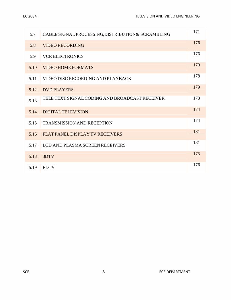
5.7 CABLE SIGNAL PROCESSING,DISTRIBUTION& SCRAMBLING171
5.8 VIDEO RECORDING176
5.9 VCR ELECTRONICS176
5.10 VIDEO HOME FORMATS179
5.11 VIDEO DISC RECORDING AND PLAYBACK178
5.12 DVD PLAYERS179
5.13TELE TEXT SIGNAL CODING AND BROADCAST RECEIVER 173
5.14 DIGITAL TELEVISION174
5.15 TRANSMISSION AND RECEPTION174
5.16 FLAT PANEL DISPLAY TV RECEIVERS181
5.17 LCD AND PLASMA SCREEN RECEIVERS181
5.18 3DTV175
5.19 EDTV176
SCE 8 ECE DEPARTMENT

EC 2034 TELEVISION AND VIDEO ENGINEERING
UNIT I
FUNDAMENTALS OF TELEVISION
1.1.ASPECT RATIO
The frame adopted in all television systems is rectangular with width/height ratio, i.e.,aspect ratio = 4/3. There are many reasons for this choice. In human affairs most of themotion occurs in the horizontal plane and so a larger width is desirable.
The eyes can view with more ease and comfort when the width of a picture is more thanits height. The usage of rectangular frame in motion pictures with a width/height ratio of4/3 is another important reason for adopting this shape and aspect ratio.
This enables direct television transmission of film programmes without wastage of anyfilm area.
It is not necessary that the size of the picture produced on the receiver screen be same asthat being televised but it is essential that the aspect ratio of the two be same, otherwisethe scene details would look too thin or too wide.
This is achieved by setting the magnitudes of the current in the deflection coils to correctvalues, both at the TV camera and receiving picture tube.
Another important requirement is that the same coordinates should be scanned at anyinstant both by the camera tube beam and the picture tube beam in the receiver.Synchronizing pulses are transmitted along with the picture information to achieve exactcongruence between transmitter and receiver scanning systems.
1.2.IMAGE CONTINUITY
While televising picture elements of the frame by means of the scanning process, it isnecessary to present the picture to the eye in such a way that an illusion of continuity iscreated and any motion in the scene appears on the picture tube screen as a smooth andcontinuous change.
To achieve this, advantage is taken of ‘persistence of vision’ or storage characteristics ofthe human eye. This arises from the fact that the sensation produced when nerves of theeye’s retina are stimulated by incident light does not cease immediately after the light isremoved but persists for about 1/16th of a second.
Thus if the scanning rate per second is made greater than sixteen, or the number ofpictures shown per second is more than sixteen, the eye is able to integrate the changinglevels of brightness in the scene. So when the picture elements are scanned rapidlyenough, they appear to the eye as a complete picture unit, with none of the individualelements visible separately.
In present day motion pictures twenty-four still pictures of the scene are taken per secondand later projected on the screen at the same rate. Each picture or frame is projectedindividually as a still picture, but they are shown one after the other in rapid succession toproduce the illusion of continuous motion of the scene being shown.
SCE 9 ECE DEPARTMENT
EC 2034 TELEVISION AND VIDEO ENGINEERING
A shutter in the projector rotates in front of the light source and allows the film to beprojected on the screen when the film frame is still, but blanks out any light from thescreen during the time when the next film frame is being moved into position.
As a result, a rapid succession of still-film frames is seen on the screen. With all lightremoved during the change from one frame to the next, the eye sees a rapid sequence ofstill pictures that provides the illusion of continuous motion. Scanning. A similar processis carried out in the television system.
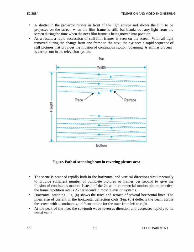
Figure. Path of scanning beam in covering picture area
The scene is scanned rapidly both in the horizontal and vertical directions simultaneouslyto provide sufficient number of complete pictures or frames per second to give theillusion of continuous motion. Instead of the 24 as in commercial motion picture practice,the frame repetition rate is 25 per second in most television systems.
Horizontal scanning. Fig. (a) shows the trace and retrace of several horizontal lines. Thelinear rise of current in the horizontal deflection coils (Fig. (b)) deflects the beam acrossthe screen with a continuous, uniform motion for the trace from left to right.
At the peak of the rise, the sawtooth wave reverses direction and decreases rapidly to itsinitial value.
SCE 10 ECE DEPARTMENT

EC 2034 TELEVISION AND VIDEO ENGINEERING
This fast reversal produces the retrace or flyback. The start of the horizontal trace is at theleft edge of raster. The finish is at the right edge, where the flyback produces retrace backto the left edge. Note, that ‘up’ on the sawtooth wave corresponds to horizontal deflectionto the right. The heavy lines in Fig. (a) indicate the useful scanning time and the dashedlines correspond to the retrace time.
Vertical scanning. The sawtooth current in the vertical deflection coils (see Fig.) movesthe electron beam from top to bottom of the raster at a uniform speed while the electronbeam is being deflected horizontally.
Thus the beam produces complete horizontal lines one below the other while movingfrom top to bottom. As shown in Fig. (c), the trace part of the sawtooth wave for verticalscanning deflects the beam to the bottom of the raster. Then the rapid vertical retracereturns the beam to the top.
Note that the maximum amplitude of the vertical sweep current brings the beam to thebottom of the raster. As shown in Fig. (b) during vertical retrace the horizontal scanningcontinues and several lines get scanned during this period. Because of motion in thescene being televised, the information or brightness at the top of the target plate or picturetube screen normally changes by the time the beam returns to the top to recommence thewhole process.
This information is picked up during the next scanning cycle and the whole process isrepeated 25 times to cause an illusion of continuity. The actual scanning sequence ishowever a little more complex than that just described and is explained in a later sectionof this chapter. It must however be noted, that both during horizontal retrace and verticalretrace intervals the scanning beams at the camera tube and picture tube are blanked andno picture information is either picked up or reproduced.
Instead, on a time division basis, these short retrace intervals are utilized for transmittingdistinct narrow pulses to keep the sweep oscillators of the picture tube deflection circuitsof the receiver in synchronism with those of the camera at the transmitter.
This ensures exact correspondence in scanning at the two ends and results in distortionless reproduction of the picture details.
Figure. Waveform of current in the horizontal deflection coils producing linear (constantvelocity) scanning in the horizontal direction.
SCE 11 ECE DEPARTMENT

EC 2034 TELEVISION AND VIDEO ENGINEERING
SCE 1212
ECE DEPARTMENT
1.3.NUMBER OF SCANNING LINES
Most scenes have brightness gradations in the vertical direction. The ability of thescanning beam to allow reproduction of electrical signals according to these variationsand the capability of the human eye to resolve these distinctly, while viewing thereproduced picture, depends on the total number of lines employed for scanning.
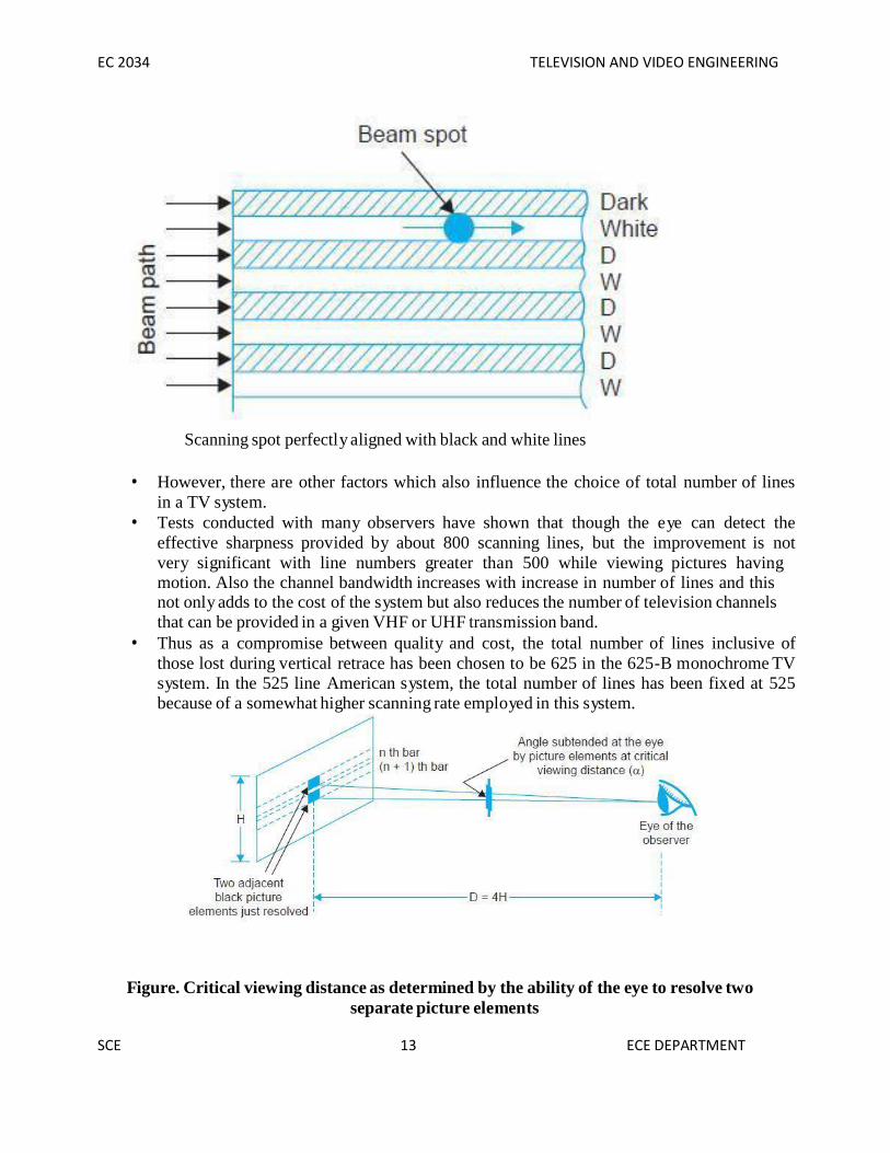
It is possible to arrive at some estimates of the number of lines necessary by consideringthe bar pattern shown in Fig. (a), where alternate lines are black and white. If thethickness of the scanning beam is equal to the width of each white and black bar, and thenumber of scanning lines is chosen equal to the number of bars, the electrical informationcorresponding to the brightness of each bar will be correctly reproduced during thescanning process.
Obviously the greater the number of lines into which the picture is divided in the verticalplane, the better will be the resolution.However, the total number of lines that need beemployed is limited by the resolving capability of the human eye at the minimumviewing distance.
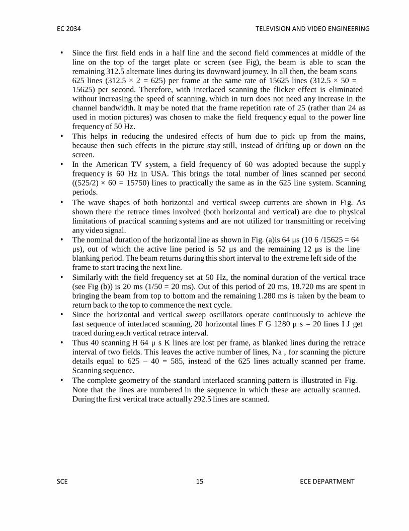
The maximum number of alternate light and dark elements (lines) which can be resolvedby the eye is given by 1N v = αρ where N v = total number of lines (elements) to beresolved in the vertical direction, α = minimum resolving angle of the eye expressed inradians, and ρ = D/H = viewing-distance/picture height.
For the eye this resolution is determined by the structure of the retina, and the brightnesslevel of the picture. it has been determined experimently that with reasonable brightnessvariations and a minimum viewing distance of four times the picture height (D/H = 4),the angle that any two adjacent elements must subtend at the eye for distinct resolution isapproximately one minute (1/60 degree). This is illustrated in Fig (b). Substituting thesevalues of α and ρ we get 1 ≈ 860 ( π / 180 × 1 / 60 ) × 4
Thus if the total number of scanning lines is chosen close to 860 and the scanning beamas illustrated in Fig. (a) just passes over each bar (line) separately while scanning all thelines from top to bottom of the picture frame, a distinct pick up of the picture informationresults and this is the best that can be expected from the system.
This perhaps explains the use of 819 lines in the original French TV system. In practicehowever, the picture elements are not arranged as equally spaced segments but haverandom distribution of black, grey and white depending on the nature of the picturedetails or the scene under consideration.
Statistical analysis and subjective tests carried out to determine the average number ofeffective lines suggest that about 70 per cent of the total lines or segments get separatelyscanned in the vertical direction and the remaining 30 per cent get merged with otherelements due to the beam spot falling equally on two consecutive lines.
This is illustrated in Fig.(c). Thus the effective number of lines distinctly resolved, i.e., Nr = N v × k, where k is the resolution factor whose value lies between 0.65 to 0.75.Assuming the value of k = 0.7 we get, N r = N v × k = 860 × 0.7 = 602.
EC 2034 TELEVISION AND VIDEO ENGINEERING
SCE 1313
ECE DEPARTMENT
Scanning spot perfectly aligned with black and white lines
However, there are other factors which also influence the choice of total number of linesin a TV system.
Tests conducted with many observers have shown that though the eye can detect theeffective sharpness provided by about 800 scanning lines, but the improvement is notvery significant with line numbers greater than 500 while viewing pictures havingmotion. Also the channel bandwidth increases with increase in number of lines and thisnot only adds to the cost of the system but also reduces the number of television channelsthat can be provided in a given VHF or UHF transmission band.
Thus as a compromise between quality and cost, the total number of lines inclusive ofthose lost during vertical retrace has been chosen to be 625 in the 625-B monochrome TVsystem. In the 525 line American system, the total number of lines has been fixed at 525because of a somewhat higher scanning rate employed in this system.
Figure. Critical viewing distance as determined by the ability of the eye to resolve twoseparate picture elements

EC 2034 TELEVISION AND VIDEO ENGINEERING
SCE 1414
ECE DEPARTMENT
Figure. Scanning beam focused on the junction of black and white lines.
1.4. INTERLACED SCANNING
Interlaced scanning. In television pictures an effective rate of 50 vertical scans per secondis utilized to reduce flicker. This is accomplished by increasing the downward rate oftravel of the scanning electron beam, so that every alternate line gets scanned instead ofevery successive line.
Then, when the beam reaches the bottom of the picture frame, it quickly returns to the topto scan those lines that were missed in the previous scanning. Thus the total number oflines are divided into two groups called ‘fields’. Each field is scanned alternately. Thismethod of scanning is known as interlaced scanning and is illustrated in Fig. It reducesflicker to an acceptable level since the area of the screen is covered at twice the rate.
This is like reading alternate lines of a page from top to bottom once and then going backto read the remaining lines down to the bottom.In the 625 lime monochrome system, forsuccessful interlaced scanning, the 625 lines of each frame or picture are divided into setsof 312.5 lines and each set is scanned alternately to cover the entire picture area.
To achieve this the horizontal sweep oscillator is made to work at a frequency of 15625Hz (312.5 × 50 = 15625) to scan the same number of lines per frame (15625/25 = 625lines), but the vertical sweep circuit is run at a frequency of 50 instead of 25 Hz.
Note that since the beam is now deflected from top to bottom in half the time and thehorizontal oscillator is still operating at 15625 Hz, only half the total lines, i.e., 312.5(625/2 = 312.5) get scanned during each vertical sweep.
EC 2034 TELEVISION AND VIDEO ENGINEERING
SCE 1515
ECE DEPARTMENT
Since the first field ends in a half line and the second field commences at middle of theline on the top of the target plate or screen (see Fig), the beam is able to scan theremaining 312.5 alternate lines during its downward journey. In all then, the beam scans625 lines (312.5 × 2 = 625) per frame at the same rate of 15625 lines (312.5 × 50 =15625) per second. Therefore, with interlaced scanning the flicker effect is eliminatedwithout increasing the speed of scanning, which in turn does not need any increase in thechannel bandwidth. It may be noted that the frame repetition rate of 25 (rather than 24 asused in motion pictures) was chosen to make the field frequency equal to the power linefrequency of 50 Hz.
This helps in reducing the undesired effects of hum due to pick up from the mains,because then such effects in the picture stay still, instead of drifting up or down on thescreen.
In the American TV system, a field frequency of 60 was adopted because the supplyfrequency is 60 Hz in USA. This brings the total number of lines scanned per second((525/2) × 60 = 15750) lines to practically the same as in the 625 line system. Scanningperiods.
The wave shapes of both horizontal and vertical sweep currents are shown in Fig. Asshown there the retrace times involved (both horizontal and vertical) are due to physicallimitations of practical scanning systems and are not utilized for transmitting or receivingany video signal.
The nominal duration of the horizontal line as shown in Fig. (a)is 64 μs (10 6 /15625 = 64μs), out of which the active line period is 52 μs and the remaining 12 μs is the lineblanking period. The beam returns during this short interval to the extreme left side of theframe to start tracing the next line.
Similarly with the field frequency set at 50 Hz, the nominal duration of the vertical trace(see Fig (b)) is 20 ms (1/50 = 20 ms). Out of this period of 20 ms, 18.720 ms are spent inbringing the beam from top to bottom and the remaining 1.280 ms is taken by the beam toreturn back to the top to commence the next cycle.
Since the horizontal and vertical sweep oscillators operate continuously to achieve thefast sequence of interlaced scanning, 20 horizontal lines F G 1280 μ s = 20 lines I J gettraced during each vertical retrace interval.
Thus 40 scanning H 64 μ s K lines are lost per frame, as blanked lines during the retraceinterval of two fields. This leaves the active number of lines, Na , for scanning the picturedetails equal to 625 – 40 = 585, instead of the 625 lines actually scanned per frame.Scanning sequence.
The complete geometry of the standard interlaced scanning pattern is illustrated in Fig.Note that the lines are numbered in the sequence in which these are actually scanned.During the first vertical trace actually 292.5 lines are scanned.

EC 2034 TELEVISION AND VIDEO ENGINEERING
SCE 1616
ECE DEPARTMENT
Figure. Principle of interlaced scanning. Note that the vertical retrace time has beenassumed to be zero
The beam starts at A, and sweeps across the frame with uniform velocity to cover all thepicture elements in one horizontal line. At the end of this trace the beam then retracesrapidly to the left side of the frame as shown by the dashed line in the illustration to beginthe next horizontal line.
Note that the horizontal lines slope downwards in the direction of scanning because thevertical deflecting current simultaneously produces a vertical scanning motion, which isvery slow compared with horizontal scanning. The slope of the horizontal trace from leftto right is greater than during retrace from right to left.
The reason is that the faster retrace does not allow the beam so much time to be deflectedvertically. After line one, the beam is at the left side ready to scan line 3, omitting thesecond line.
However, as mentioned earlier it is convenient to number the lines as they are scannedand so the next scanned line skipping one line, is numbered two and not three. Thisprocess continues till the last line gets scanned half when the vertical motion reaches thebottom of the raster or frame.
As explained earlier skipping of lines is accomplished by doubling the vertical scanningfrequency from the frame or picture repetition rate of 25 to the field frequency of 50 Hz.With the field frequency of 50 Hz the height of the raster is so set that 292.5 lines getscanned as the beam travels from top to bottom and reaches point B.

EC 2034 TELEVISION AND VIDEO ENGINEERING
SCE 1717
ECE DEPARTMENT
Now the retrace starts and takes a period equal to 20 horizontal line periods to reach thetop marked C.
Figure. Horizontal deflection current
Figure. Vertical deflection current
These 20 lines are known as inactive lines, as the scanning beam is cut-off during thisperiod. Thus the second field starts at the middle of the raster and the first line scanned isthe 2nd half of line number 313.
The scanning of second field, starting at the middle of the raster automatically enables thebeam to scan the alternative lines left un-scanned during the first field. The verticalscanning motion otherwise is exactly the same as in the previous field giving all thehorizontal lines the same slope downwards in the direction of scanning.
As a result 292.5 lines again get scanned and the beam reaches the bottom of the framewhen it has completed full scanning of line number 605.
The inactive vertical retrace again begins and brings the beam back to the top at point Ain a period during which 20 blanked horizontal lines (605 to 625) get scanned. Back atpoint A, the scanning beam has just completed two fields or one frame and is ready tostart the third field covering the same area (no. of lines) as scanned during the first field.This process (of scanning fields) is continued at a fast rate of 50 times a second, which

EC 2034 TELEVISION AND VIDEO ENGINEERING
SCE 1818
ECE DEPARTMENT
not only creates an illusion of continuity but also solves the problem of flickersatisfactorily.
Figure. Odd line interlaced scanning procedure.
1.6. TELEVISION CAMERA TUBES
A TV camera tube may be called the eye of a TV system. For such an analogy to becorrect the tube must possess characteristic that are similar to its human counterpart.Some of the more important functions must be,(i) sensitivity to visible light, (ii) wide dynamic range with respect to light intensity, and
(iii) ability to resolve details while viewing a multi-element scene. During the development of television, the limiting factor on the ultimate performance had
always been the optical-electrical conversion device, i.e., the pick-up tube.
Most types developed have suffered to a greater or lesser extent from (i) poor sensitivity,(ii) poor resolution, (iii) high noise level, (iv) undesirable spectral response, (v)instability, (vi) poor contrast range and (vii) difficulties of processing. However,development work during the past fifty years or so, has enabled scientists and engineersto develop image pick-up tubes, which not only meet the desired requirements but in factexcel the human eye in certain respects.
Such sensitive tubes have now been developed which deliver output even where our eyessee complete darkness. Spectral response has been so perfected, that pick-up outside thevisible range (in infra-red and ultraviolet regions) has become possible. In fact, now thereis a tube available for any special application.

EC 2034 TELEVISION AND VIDEO ENGINEERING
SCE 1919
ECE DEPARTMENT
BASIC PRINCIPLE
When minute details of a picture are taken into account, any picture appears to becomposed of small elementary areas of light or shade, which are known as pictureelements. The elements thus contain the visual image of the scene.
The purpose of a TV pick-up tube is to sense each element independently and develop asignal in electrical form proportional to the brightness of each element. As alreadyexplained in Chapter 1, light from the scene is focused on a photosensitive surface knownas the image plate, and the optical image thus formed with a lens system represents lightintensity variations of the scene.
The photoelectric properties of the image plate then convert different light intensities intocorresponding electrical variations.
In addition to this photoelectric conversion whereby the optical information is transducedto electrical charge distribution on the photosensitive image plate, it is necessary to pick-up this information as fast as possible. Since simultaneous pick-up is not possible,scanning by an electron beam is resorted to.
The electron beam moves across the image plate line by line, and field by field to providesignal variations in a successive order. This scanning process divides the image into itsbasic picture elements. Through the entire image plate is photoelectric, its constructionisolates the picture elements so that each discrete small area can produce its own signalvariations.
Photoelectric Effects
The two photoelectric effects used for converting variations of light intensity intoelectrical variations are (i) photoemission and (ii) photoconductivity. Certain metals emitelectrons when light falls on their surface.
These emitted electrons are called photoelectrons and the emitting surface aphotocathode. Light consists of small bundles of energy called photons. When light ismade incident on a photocathode, the photons give away their energy to the outer valenceelectrons to allow them to overcome the potential-energy barrier at the surface.
The number of electrons which can overcome the potential barrier and get emitted,depends on the light intensity. Alkali metals are used as photocathode because they havevery low work-function.
Cesium-silver or bismuth-silver-cesium oxides are preferred as photo emissive surfacesbecause they are sensitive to incandescent light and have spectral response very close tothe human eye. The second method of producing an electrical image is byphotoconduction, where the conductivity or resistivity of the photosensitive surfacevaries in proportion to the intensity of light focused on it.
In general the semiconductor metals including selenium, tellurium and lead with theiroxides have this property known as photoconductivity. The variations in resistance ateach point across the surface of the material is utilized to develop a varying signal byscanning it uniformly with an electron beam. Image Storage Principle Television camerasdeveloped during the initial stages of development were of the non-storage type, where

EC 2034 TELEVISION AND VIDEO ENGINEERING
SCE 2020
ECE DEPARTMENT
the signal output from the camera for the light on each picture element is produced onlyat the instant it is scanned.
Most of the illumination is wasted. Since the effect of light on the image plate cannot bestored, any instantaneous pick-up has low sensitivity. Image di-sector and flying-spotcamera are examples of non-storage type of tubes. These are no longer in use and will notbe discussed.
High camera sensitivity is necessary to televise scenes at low light levels and to achievethis, storage type tubes have been developed. In storage type camera tubes the effect ofillumination on every picture element is allowed to accumulate between the times it isscanned in successive frames. With light storage tubes the amount of photoelectric signalan be increased 10,000 times approximately compared with the earlier non-storage type.
The Electron Scanning Beam
As in the case of picture tubes an electron gun produces a narrow beam of electrons forscanning. In camera tubes magnetic focusing is normally employed. The electrons mustbe focused to a very narrow and thin beam because this is what determines the resolvingcapability of the camera.
The diameter of the beam determines the size of the smallest picture element and hencethe finest detail of the scene to which it can be resolved. Any movement of electriccharge is a flow of current and thus the electron beam constitutes a very small currentwhich leaves the cathode in the electron gun and scans the target plate.
The scanning is done by deflecting the beam with the help of magnetic fields producedby horizontal and vertical coils in the deflection yoke put around the tubes. The beamscans 312.5 lines per field and 50 such fields are scanned per second.
Video Signal
In tubes employing photo emissive target plates the electron beam deposits some chargeon the target plate, which is proportional to the light intensity variations in the scenebeing televised.
The beam motion is so controlled by electric and magnetic fields, that it is deceleratedbefore it reaches the target and lands on it with almost zero velocity to avoid anysecondary emission.
Because of the negative acceleration the beam is made to move back from the target andon its return journey, which is very accurately controlled by the focusing and deflectioncoils, it strikes an electrode which is located very close to the cathode from where itstarted. The number of electrons in the returning beam will thus vary in accordance withthe charge deposited on the target plate.
This in turn implies that the current which enters the collecting electrode varies inamplitude and represents brightness variations of the picture. This current is finally madeto flow through a resistance and the varying voltage developed across this resistanceconstitutes the video signal. Figure (a) illustrates the essentials of this technique ofdeveloping video signal.In camera tubes employing photoconductive cathodes thescanning electron beam causes a flow of current through the photoconductive material.

EC 2034 TELEVISION AND VIDEO ENGINEERING
SCE 2121
ECE DEPARTMENT
The amplitude of this current varies in accordance with the resistance offered by thesurface at different points. Since the conductivity of the material varies in accordancewith the light falling on it, the magnitude of the current represents the brightnessvariations of the scene.
This varying current completes its path under the influence of an applied dc voltagethrough a load resistance connected in series with path of the current. The instantaneousvoltage developed across the load resistance is the video signal which, after dueamplification and processing is amplitude modulated and transmitted.
Figure (b) shows a simplified illustration of this method of developing videosignal.Electron Multiplier When the surface of a metal is bombarded by incidentelectrons having high velocities, secondary emission takes place.
Aluminium, as an example, can release several secondary electrons for each incidentprimary electron. Camera tubes often include an electron multiplier structure, making useof the secondary emission effect to amplify the small amount of photoelectric current thatis later employed to develop video signal.
The electron multiplier is a series of cold anode- cathode electrodes called dynodesmounted internally, with each at a progressively higher positive potential as illustrated inFig. The few electrons emitted by the photocathode are accelerated to a more positivedynode.
The primary electrons can then force the ejection of secondary emission electrons whenthe velocity of the incident electrons is large enough. The secondary emission ratio isnormally three or four, depending on the surface and the potential applied.
Figure. Production of video signal by photoemission
The number of electrons available is multiplied each time the secondary electrons strikethe emitting surface of the next more positive dynode. The current amplification thusobtained is noise free because the electron multiplier does not have any active device orresistors.

EC 2034 TELEVISION AND VIDEO ENGINEERING
SCE 2222
ECE DEPARTMENT
Since the signal amplitude is very low any conventional amplifier, if used instead of theelectron multiplier, would cause serious S/N ratio problems
Figure. Production of video signal by photoconduction.
Figure. Illustration of an electron-multiplier structure.

EC 2034 TELEVISION AND VIDEO ENGINEERING
1.7. IMAGE ORTHICON
This tube makes use of the high photo emissive sensitivity obtainable fromphotocathodes, image multiplication at the target caused by secondary emission and anelectron multiplier.
A sectional view of an image orthicon is shown in Fig. It has three main sections: imagesection, scanning section and electron gun-cum-multiplier section. (i) Image Section Theinside of the glass face plate at the front is coated with a silver, antimony coatingsensitized with cesium, to serve as photocathode.
Light from the scene to be televised is focused on the photocathode surface by a lenssystem and the optical image thus formed results in the release of electrons from eachpoint on the photocathode in proportion to the incident light intensity. Photocathodesurface is semitransparent and the light rays penetrate it to reach its inner surface fromwhere electron emission takes place.
Since the number of electrons emitted at any point in the photocathode has a distributioncorresponding to the brightness of the optical image, an electron image of the scene orpicture gets formed on the target side of the photo coating and extends towards it.Through the conversion efficiency of the photocathode is quite high, it cannot storecharge being a conductor.
For this reason, the electron image produced at the photocathode is made to movetowards the target plate located at a short distance from it. The target plate is made of avery thin sheet of glass and can store the charge received by it.
This is maintained at about 400 volts more positive with respect to the photocathode, andthe resultant electric field gives the desired acceleration and motion to the emittedelectrons towards it. The electrons, while in motion, have a tendency to repel each otherand thin can result in distortion of the information now available as charge image. Toprevent this divergence effect an axial magnetic field, generated in this region by the‘long focus coil’ is employed.
This magnetic field imparts helical motion of increasing pitch and focuses the emittedelectrons on the target into a well-defined electron image of the original optical image.The image side of the target has a very small deposit of cesium and thus has a highsecondary emission ratio.
Because of the high velocity attained by the electrons while in motion from photocathodeto the target plate, secondary emission results, as the electrons bombard the targetsurface.
These secondary electrons are collected by a wire-mesh screen, which is located in frontof the target on the image side and is maintained at a slightly higher potential with respectto the target.
SCE 23 ECE DEPARTMENT

EC 2034 TELEVISION AND VIDEO ENGINEERING
SCE 2424
ECE DEPARTMENT
The wire-mesh screen has about 300 meshes per cm 2 with an open area of 50 to 75 percent, so that the screen wires do not interfere with the electron image.
The secondary electrons leave behind on the target plate surface, a positive chargedistribution, corresponding to the light intensity distribution on the original photocathode.For storage action this charge on the target plate should not spread laterally over itssurface, during the storage time, since this would destroy the resolution of the device.
To achieve this the target is made out of extremely thin sheet of glass. The positivecharge distribution builds up during the frame storage time (40 ms) and thus enhances thesensitivity of the tube. It should be clearly understood, that the light from the scene beingtelevised continuously falls on the photocathode, and the resultant emitted electrons onreaching the target plate cause continuous secondary emission. This continuous release ofelectrons results in the building up of positive charge on the target plate.
Because of the high secondary emission ratio, the intensity of the positive chargedistribution is four to five times more as compared to the charge liberated by the photocathode.
This increase in charge density relative to the charge liberated at the photocathode isknown as ‘image multiplication’ and contributes to the increased sensitivity of imageorthicon. As shown in Fig., the two-sided target has the charge image on one side whilean electron beam scans the opposite side.
Thus, while the target plate must have high resistivity laterally for storage action, it musthave low resistivity along its thickness, to enable the positive charge to conduct to theother side which is scanned.

EC 2034 TELEVISION AND VIDEO ENGINEERING
SCE 2525
ECE DEPARTMENT
It is for this reason that the target plate is very thin, with thickness close to 0.004 mm.Thus, whatever charge distribution builds up on one side of the target plate due to thefocused image, appears on the other side, which is scanned, and it is from here that thevideo signal is obtained.
(ii) Scanning Section The electron gun structure produces a beam of electrons that is accelerated towards the
target. As indicated in the figure, positive accelerating potentials of 80 to 330 volts areapplied to grid 2, grid 3, and grid 4 which is connected internally to the metalizedconductive coating on the inside wall of the tube. The electron beam is focused at thetarget by magnetic field of the external focus coil and by voltage supplied to grid 4. Thealignment coil provides magnetic field that can be varied to adjust the scanning beam’sposition, if necessary, for correct location.
Deflection of electron beams to scan the entire target plate is accomplished by magneticfields of vertical and horizontal deflecting coils mounted on yoke external to the tube.These coils are fed from two oscillators, one working at 15625 Hz, for horizontaldeflection, and the other operating at 50 Hz, for vertical deflection. The target plate isclose to zero potential and therefore electrons in the scanning beam can be made to stoptheir forward motion at its surface and then return towards the gun structure.
The grid 4 voltage is adjusted to produce uniform deceleration of electrons for the entiretarget area. As a result, electrons in the scanning beam are slowed down near the target.This eliminates any possibility of secondary emission from this side of the target plate.
If a certain element area on the target plate reaches a potential of, say, 2 volts during thestorage time, then as a result of its thinness the scanning beam ‘sees’ the charge depositedon it, part of which gets diffused to the scanned side and deposits an equal number ofnegative charges on the opposite side.
Thus out of the total electrons in the beam, some get deposited on the target plate, whilethe remaining stop at its surface and turn back to go towards the first electrode of theelectron multiplier. Because of low resistivity across the two sides of the target, thedeposited negative charge neutralizes the existing positive charge in less than a frametime.
The target can again become charged as a result of the incident picture information, to bescanned during the successive frames. As the target is scanned element by element, ifthere are no positive charges at certain points, all the electrons in the beam return towardsthe electron gun and none gets deposited on the target plate.
The number of electrons, leaving cathode of the gun, is practically constant, and out ofthis, some get deposited and remaining electrons, which travel backwards provide signalcurrent that varies in amplitude in accordance with the picture information.
Obviously then, the signal current is maximum for black areas on the picture, becauseabsence of light from black areas on the picture does not result in any emission on thephotocathode, and there is no secondary emission at the corresponding points on thetarget, and no electrons are needed from the beam to neutralize them.
On the contrary for high light areas, on the picture, there is maximum loss of electronsfrom the target plate, due to secondary emission, and this results in large deposits ofelectrons from the beam and this reduces the amplitude of the returning beam current.The resultant beam current that turns away from the target, is thus, maximum for black

EC 2034 TELEVISION AND VIDEO ENGINEERING
SCE 2626
ECE DEPARTMENT
areas and minimum for bright areas on the picture. High intensity light causes largecharge imbalance on the glass target plate.
The scanning beam is not able to completely neutralize it in one scan. Therefore theearlier impression persists for several scans. Image Resolution. It may be mentioned atthis stage that since the beam is of low velocity type, being reduced to near zero velocityin the region of the target it is subjected to stray electric fields in its vicinity, which cancause defocusing and thus loss of resolution.
Also on contact with the target, the electrons would normally glide along its surfacetangentially for a short distance and the point of contact becomes ill defined. The beammust strike the target at right angle at all points of the target, for better resolution. Thesedifficulties are overcome in the image-orthicon by the combined action of electrostaticfield because of potential on grid 4, and magnetic field of the long focusing coil.
The interaction of two fields gives rise to cyclical motion to the beam in the vicinity oftarget, which then hits it at right angle no matter which point is being scanned. This verymuch improves the resolving capability of the picture tube.
(iii) Electron Multiplier The returning stream of electrons arrive at the gun close to the aperture from which
electron beam emerged. The aperture is a part of a metal disc covering the gun electrode.When the returning electrons strike the disc which is at a positive potential of about 300volts, with respect to the target, they produce secondary emission.
The disc serves as first stage of the electron multiplier. Successive stages of the electronmultiplier are arranged symmetrically around and back of the first stage. Thereforesecondary electrons are attracted to the dynodes at progressively higher positivepotentials. Five stages of multiplication are used, details of which are shown in Fig. Eachmultiplier stage provides a gain of approximately 4 and thus a total gain of (4) 5 ≈ 1000 isobtained at the electron multiplier. This is known as signal multiplication.
The multiplication so obtained maintains a high signal to noise ratio. The secondaryelectrons are finally collected by the anode, which is connected to the highest supplyvoltage of + 1500 volts in series with a load resistance R L . The anode current through RL has the same variations that are present in the return beam from the target andamplified by the electron multiplier.
Therefore voltage across R L is the desired video signal; the amplitude of which varies inaccordance with light intensity variations of scene being televised. The output across R Lis capacitive coupled to the camera signal amplifier. With R L = 20 K-ohms and typicaldark and high light currents of magnitudes 30 μA and 5 μA respectively, the cameraoutput signal will have an amplitude of 500 mV peak-to-peak.
Field Mesh Image Orthicon. The tube described above is a non-field mesh imageorthicon. In some designs an additional pancake-shaped magnetic coil is provided in frontof the face plate. This is connected in series with the main focusing coil.
The location of the coil results in a graded magnetic field such that the optically focusedphotocathode image is magnified by about 1.5 times. Thus the charge image produced onthe target plate is bigger in size and this results in improved resolution and better overallperformance. Such a camera tube is known as a field mesh Image Orthicon.

EC 2034 TELEVISION AND VIDEO ENGINEERING
SCE 2727
ECE DEPARTMENT
Figure. Electron-multiplier section of the Image Orthicon.
Light Transfer Characteristics and Applications
During the evolution of image orthicon tubes, two separate types were developed, onewith a very close target-mesh spacing (less than 0.001 cm) and the other with somewhatwider spacing.
The tube, with very close target mesh spacing, has very high signal to noise ratio but thisis obtained at the expense of sensitivity and contrast ratio.
This is a worthwhile exchange where lighting conditions can be controlled and picturequality is of primary importance. This is generally used for live shows in the studios.
The other type with wider target-mesh spacing has high sensitivity and contrast ratio withmore desirable spectral response.
This tube has wider application for outdoor or other remote pickups where a wide rangeof lighting conditions have to be accommodated. More recent tubes with improvedphotocathodes have sensitivities several times those of previous tubes and muchimproved spectral response.
Overall transfer characteristics of such tubes are drawn in Fig. Tube ‘A’ is intendedprimarily for outdoor pick-ups where as tube ‘B’ is much suited for studio use andrequires strong illumination.
The knee of the transfer characteristics is reached when the illumination causes the targetto be fully charged with respect to the mesh between successive scans by the electronbeam.

EC 2034 TELEVISION AND VIDEO ENGINEERING
SCE 2828
ECE DEPARTMENT
The tube is sometimes operated slightly above the knee, to obtain the black border effect(also known as Halo effect) around the high light areas of the target.
Figure. Light transfer characteristics of two different Image Orthicons.
1.8. VIDICON The Vidicon came into general use in the early 50’s and gained immediate popularity
because of its small size and ease of operation. It functions on the principle ofphotoconductivity, where the resistance of the target material shows a marked decreasewhen exposed to light. illustrates the structural configuration of a typical vidicon, andFig.
Figure. Vidicon camera tube cross-section.

EC 2034 TELEVISION AND VIDEO ENGINEERING
SCE 2929
ECE DEPARTMENT
Shows the circuit arrangement for developing camera signal output. As shown there, thetarget consists of a thin photo conductive layer of either selenium or anti-monycompounds.
This is deposited on a transparent conducting film, coated on the inner surface of the faceplate. This conductive coating is known as signal electrode or plate. Image side of thephotolayer, which is in contact with the signal electrode, is connected to DC supplythrough the load resistance RL.
The beam that emerges from the electron gun is focused on surface of the photoconductive layer by combined action of uniform magnetic field of an external coil andelectrostatic field of grid No 3. Grid No. 4 provides a uniform decelerating field betweenitself, and the photo conductive layer, so that the electron beam approaches the layer witha low velocity to prevent any secondary emission.
Deflection of the beam, for scanning the target, is obtained by vertical and horizontaldeflecting coils, placed around the tube.
Figure. Schematic representation of a Vidicon target area.
Charge Image The photo layer has a thickness of about 0.0001 cm, and behaves like an insulator with a
resistance of approximately 20 MΩ when in dark. With light focused on it, the photonenergy enables more electrons to go to the conduction band and this reduces itsresistivity.
When bright light falls on any area of the photoconductive coating, resistance across thethickness of that portion gets reduces to about 2 MΩ. Thus, with an image on the target,
EC 2034 TELEVISION AND VIDEO ENGINEERING
SCE 3030
ECE DEPARTMENT
each point on the gun side of the photo layer assumes a certain potential with respect tothe DC supply, depending on its resistance to the signal plate.
For example, with a B + source of 40 V (see Fig), an area with high illumination mayattain a potential of about + 39 V on the beam side. Similarly dark areas, on account ofhigh resistance of the photo layer may rise to only about + 35 volts.
Thus, a pattern of positive potentials appears, on the gun side of the photo layer,producing a charge image, that corresponds to the incident optical image.
Storage Action Though light from the scene falls continuously on the target, each element of the photo
coating is scanned at intervals equal to the frame time. This results in storage action andthe net change in resistance, at any point or element on the photoconductive layer,depends on the time, which elapses between two successive scanning and the intensity ofincident light.
Since storage time for all points on the target plate is same, the net change in resistance ofall elementary areas is proportional to light intensity variations in the scene beingtelevised. Signal Current As the beam scans the target plate, it encounters differentpositive potentials on the side of the photo layer that faces the gun.
Sufficient number of electrons from the beam are then deposited on the photo layersurface to reduce the potential of each element towards the zero cathode potential. Theremaining electrons, not deposited on the target, return back and are not utilized in thevidicon.
However, the sudden change in potential on each element while the beam scans, causes acurrent flow in the signal electrode circuit producing a varying voltage across the loadresistance R L. Obviously, the amplitude of current and the consequent output voltageacross R L are directly proportional to the light intensity variations on the scene.
Note that, since, a large current would cause a higher voltage drop across R L , the outputvoltage is most negative for white areas. The video output voltage, that thus developsacross the load resistance (50 K-ohms) is adequate and does not need any image or signalmultiplication as in an image orthicon.
The output signal is further amplified by conventional amplifiers before it leaves thecamera unit. This makes the vidicon a much simpler picture tube. Leaky CapacitorConcept Another way of explaining the development of ‘charge image’ on the photolayer is to consider it as an array of individual target elements, each consisting of acapacitor paralleled with a light dependent resistor. A number of such representations areshown in Fig.

EC 2034 TELEVISION AND VIDEO ENGINEERING
SCE 3131
ECE DEPARTMENT
Figure. Schematic representation of a Vidicon target area.
As seen there, one end of these target elements is connected to the signal electrode andthe other end is unterminated facing the beam. In the absence of any light image, thecapacitors attain a charge almost equal to the B + (40 V) voltage in due course of time.
However, when an image is focused on the target the resistors in parallel with thecapacitors change in value depending on the intensity of light on each unit element.
For a high light element, the resistance across the capacitor drops to a fairly low value,and this permits lot of charge from the capacitor to leak away. At the time of scanning,more electrons are deposited, on the unterminated end of this capacitor to recharge it tothe full supply voltage of + 40 V. The consequent flow of current that completes its paththrough R L develops a signal voltage across it.
Similarly for black areas of the picture, the resistance across the capacitors remains fairlyhigh, and not much charge is allowed to leak from the corresponding capacitors. This inturn needs fewer number of electrons from the beam to recharge the capacitors. Theresultant small current that flows, develops a lower voltage across the load resistance.
The electron beam thus ‘sees’ the charge on each capacitor, while scanning the target,and delivers more or less number of electrons to recharge them to the supply voltage.This process is repeated every 40 ms to provide the necessary video signal correspondingto the picture details at the upper end of the load resistor.
The video signal is fed through a blocking capacitor to an amplifier for necessaryamplification.
Light Transfer Characteristics Vidicon output characteristics are shown in Fig. Each curve is for a specific value of
‘dark’ current, which is the output with no light. The ‘dark’ current is set by adjusting thetarget voltage.

EC 2034 TELEVISION AND VIDEO ENGINEERING
SCE 3232
ECE DEPARTMENT
Sensitivity and dark current both increase as the target voltage is increased. Typical output for the vidicon is 0.4 μA for bright light with a dark current of 0.02 μA.
The photoconductive layer has a time lag, which can cause smear with a trail followingfast moving objects.
The photoconductive lag increases at high target voltages, where the vidicon has itshighest sensitivity.
Figure. Light transfer characteristics of Vidicon
Applications Earlier types of vidicons were used only where there was no fast movement, because of
inherent lag. These applications included slides, pictures, closed circuit TV etc. Thepresent day improved vidicon finds wide applications in education, medicine, industry,aerospace and oceanography.
It is, perhaps, the most popular tube in the television industry. Vidicon is a short tubewith a length of 12 to 20 cm and diameter between 1.5 and 4 cm. Its life is estimated tobe between 5000 and 20,000 hours.
1.9. PLUMBICON This picture tube has overcome many of the less favorable features of standard vidicon.
It has fast response and produces high quality pictures at low light levels. Its smaller sizeand light weight, together with low-power operating characteristics, makes it an ideal tubefor transistorized television cameras. Except for the target, plumbicon is very similar tothe standard vidicon. Focus and deflection are both obtained magnetically. Its targetoperates effectively as a P–I–N semi- conductor diode.

EC 2034 TELEVISION AND VIDEO ENGINEERING
The inner surface of the faceplate is coated with a thin transparent conductive layer of tinoxide (SnO 2 ). This forms a strong N type (N + ) layer and serves as the signal plate ofthe target. On the scanning side of this layer is deposited a photoconductive layer of purelead monoxide (PbO) which is intrinsic or ‘I’ type. Finally the pure PbO is doped to forma P type semiconductor on which the scanning beam lands.
Figure. Plumbicon camera tube (a) target details (b) output signal current and (c)characteristics.
The photoconductive target of the plumbicon functions similar to the photoconductivetarget in the vidicon, except for the method of discharging each storage element.
In the standard vidicon, each element acts as a leaky capacitor, with the leakageresistance decreasing with increasing light intensity. In the plumbicon, however, eachelement serves as a capacitor in series with a reverse biased light controlled diode.
In the signal circuit, the conductive film of tin oxide (SnO 2 ), is connected to the targetsupply of 40 volts through an external load resistance R L to develop the camera outputsignal voltage.
Light from the scene being televised is focussed through the transparent layer of tin-oxideon the photoconductive lead monoxide. Without light the target prevents any conductionbecause of absence of any charge carriers and so there is little or no output current. Atypical value of dark current is around 4 nA (4 × 10 – 9 Amp).
The incidence of light on the target results in photo excitation of semiconductor junctionbetween the pure PbO and doped layer. The resultant decrease in resistance causes signalcurrent flow which is proportional to the incident light on each photo element. Theoverall thickness of the target is 10 to 20 μm.
SCE 33 ECE DEPARTMENT
EC 2034 TELEVISION AND VIDEO ENGINEERING
SCE 3434
ECE DEPARTMENT
Light Transfer Characteristics
The current output versus target illumination response of a plumbicon is shown in Fig (c).It is a straight line with a higher slope as compared to the response curve of a vidicon.The higher value of current output, i.e., higher sensitivity, is due to much reducedrecombination of photo generated electrons and holes in the intrinsic layer which containsvery few discontinuities.
For target voltages higher than about 20 volts, all the generated carriers are swept quicklyacross the target without much re-combinations and thus the tube operates in a photosaturated mode. The spectral response of the plumbicon is closer to that of the human eyeexcept in the red color region.
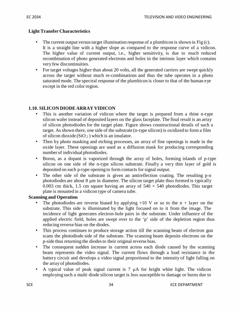
1.10. SILICON DIODE ARRAY VIDICON This is another variation of vidicon where the target is prepared from a thine n-type
silicon wafer instead of deposited layers on the glass faceplate. The final result is an arrayof silicon photodiodes for the target plate. Figure shows constructional details of such atarget. As shown there, one side of the substrate (n-type silicon) is oxidized to form a filmof silicon dioxide (SiO 2 ) which is an insulator.
Then by photo masking and etching processes, an array of fine openings is made in theoxide layer. These openings are used as a diffusion mask for producing correspondingnumber of individual photodiodes.
Boron, as a dopant is vaporized through the array of holes, forming islands of p-typesilicon on one side of the n-type silicon substrate. Finally a very thin layer of gold isdeposited on each p-type opening to form contacts for signal output.
The other side of the substrate is given an antireflection coating. The resulting p-nphotodiodes are about 8 μm in diameter. The silicon target plate thus formed is typically0.003 cm thick, 1.5 cm square having an array of 540 × 540 photodiodes. This targetplate is mounted in a vidicon type of camera tube.
Scanning and Operation The photodiodes are reverse biased by applying +10 V or so to the n + layer on the
substrate. This side is illuminated by the light focused on to it from the image. Theincidence of light generates electron-hole pairs in the substrate. Under influence of theapplied electric field, holes are swept over to the ‘p’ side of the depletion region thusreducing reverse bias on the diodes.
This process continues to produce storage action till the scanning beam of electron gunscans the photodiode side of the substrate. The scanning beam deposits electrons on thep-side thus returning the diodes to their original reverse bias.
The consequent sudden increase in current across each diode caused by the scanningbeam represents the video signal. The current flows through a load resistance in thebattery circuit and develops a video signal proportional to the intensity of light falling onthe array of photodiodes.
A typical value of peak signal current is 7 μA for bright white light. The vidiconemploying such a multi diode silicon target is less susceptible to damage or burns due to

EC 2034 TELEVISION AND VIDEO ENGINEERING
SCE 3535
ECE DEPARTMENT
excessive high lights. It also has low lag time and high sensitivity to visible light whichcan be extended to the infrared region.
A particular make of such a vidicon has the trade name of ‘Epicon’. Such camera tub eshave wide applications in industrial, educational and CCTV (closed circuit television)services.
Constructional details (enlarged) of a silicon diode array target plate.
1.11. SOLID STATE IMAGE SCANNERS The operation of solid state image scanners is based on the functioning of charge coupled
devices (CCDs) which is a new concept in metal-oxide-semiconductor (MOS) circuitry.The CCD may be thought of to be a shift register formed by a string of very closel yspaced MOS capacitors. It can store and transfer analog charge signals—either electronsor holes—that may be introduced electrically or optically. The constructional details andthe manner in which storing and transferring of charge occurs is illustrated in Fig.
he chip consists of a p-type substrate, the one side of which is oxidized to form a film ofsilicon dioxide, which is an insulator. Then by photolithographic processes, similar to

EC 2034 TELEVISION AND VIDEO ENGINEERING
SCE 3636
ECE DEPARTMENT
those used in miniature integrated circuits an array of metal electrodes, known as gates,are deposited on the insulator film.
This results in the creation of a very large number of tiny MOS capacitors on the entiresurface of the chip. The application of small positive potentials to the gate electrodesresults in the development of depletion regions just below them.
These are called potential wells. The depth of each well (depletion region) varies with themagnitude of the applied potential. As shown in Fig. (a),
Figure. A three phase n-channel MOS charge coupled device. (a) Construction (b) transferof electrons between potential wells (c) different phases of clocking voltage waveform.
The gate electrodes operate in groups of three, with every third electrode connected to acommon conductor. The spots under them serve as light sensitive elements.
When any image is focused onto the silicon chip, electrons are generated within it, butvery close to the surface. The number of electrons depends on the intensity of incidentlight. Once produced they collect in the nearby potential wells. As a result the pattern ofcollected charges represents the optical image.
Charge Transfer The charge of one element is transferred along the surface of the silicon chip by applying
a more positive voltage to the adjacent electrode or gate, while reducing the voltage on it.The minority carriers (electrons in this case) while accumulating in the so called wellsreduce their depths much like the way a fluid fills up in a container.

EC 2034 TELEVISION AND VIDEO ENGINEERING
SCE 3737
ECE DEPARTMENT
The accumulation of charge carries under the first potential wells of two consecutive triosis shown in Fig. (b) Where at instant t 1 a potential φ 1 exists at the corresponding gateelectrodes. In practice the charge transfer is effected by multiphase clock voltage pulses(see Fig. 6.12 (c)) which are applied to the gates in a suitable sequence.
The manner in which the transition takes place from potential wells under φ 1 to thoseunder φ 2 is illustrated in Fig. (b). A similar transfer moves charges from φ 2 to φ 3 andthen from φ 3 to φ 1 under the influence of continuing clock pulses.
Thus, after one complete clock cycle, the charge pattern moves one stage (three gates) tothe right. The clocking sequence continues and the charge finally reaches the end of thearray where it is collected to form the signal current.
Scanning of Television Pictures A large number of CCD arrays are packed together to form the image plate. It does not
need an electron gun, scanning beam, high voltage or vacuum envelope of a conventionalcamera tube.
The potential required to move the charge is only 5 to 10 volt. The spot under each trioserves as the resolution cell. When light image is focused on the chip, electrons aregenerated in proportion to the intensity of light falling on each cell.
Figure. Basic organization of line addressed charge transfer area imaging devices.
The principle of one-dimensional charge transfer as explained above can be integrated invarious ways to render a solid-state area image device. The straightforward approachconsists of arranging a set of linear imaging structures so that each one corresponds to ascan line in the display.
The lines are then independently addressed and read into a common output diode byapplication of driving pulses through a set of switches controlled by an address register as
EC 2034 TELEVISION AND VIDEO ENGINEERING
SCE 3838
ECE DEPARTMENT
shown in Fig To reduce capacitance, the output can be simply a small diffused diode inone corner of the array.
The charge packets emerging from any line are carried to this diode by an additionalvertical output register. In such a line addressed structure (Fig.) where the sequence ofaddressing the lines is determined by the driving circuitry, interlacing can beaccomplished in a natural way.
Cameras Employing Solid-State Scanners
CCDs have a bright future in the field of solid state imaging. Full TV line-scan arrayshave already been constructed for TV cameras. However, the quality of such sensors isnot yet suitable for normal TV studio use.
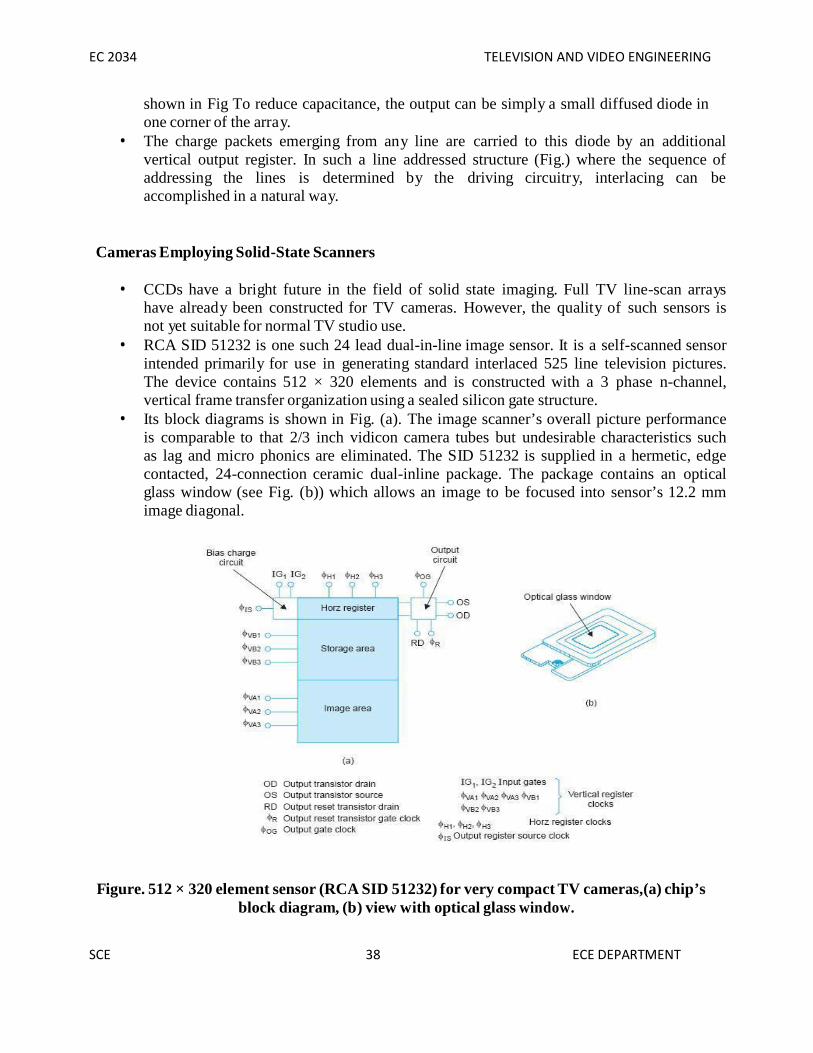
RCA SID 51232 is one such 24 lead dual-in-line image sensor. It is a self-scanned sensorintended primarily for use in generating standard interlaced 525 line television pictures.The device contains 512 × 320 elements and is constructed with a 3 phase n-channel,vertical frame transfer organization using a sealed silicon gate structure.
Its block diagrams is shown in Fig. (a). The image scanner’s overall picture performanceis comparable to that 2/3 inch vidicon camera tubes but undesirable characteristics suchas lag and micro phonics are eliminated. The SID 51232 is supplied in a hermetic, edgecontacted, 24-connection ceramic dual-inline package. The package contains an opticalglass window (see Fig. (b)) which allows an image to be focused into sensor’s 12.2 mmimage diagonal.
Figure. 512 × 320 element sensor (RCA SID 51232) for very compact TV cameras,(a) chip’sblock diagram, (b) view with optical glass window.

EC 2034 TELEVISION AND VIDEO ENGINEERING
SCE 3939
ECE DEPARTMENT
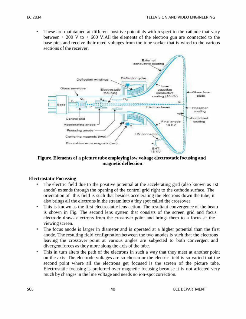
1.12. MONOCHROME PICTURE TUBE Modern monochrome picture tubes employ electrostatic focusing and electromagnetic
deflection. A typical black and white picture tube is shown in Fig. The deflection coilsare mounted externally in a specially designed yoke that is fixed close to the neck of thetube.
The coils when fed simultaneously with vertical and horizontal scanning currents deflectthe beam at a fast rate to produce the raster. The composite video signal that is injectedeither at the grid or cathode of the tube, modulates the electron beam to producebrightness variations of the tube, modulates the electron beam to produce brightnessvariations on the screen.
This results in reconstruction of the picture on the raster, bit by bit, as a function of time.However, the information thus obtained on the screen is perceived by the eye as acomplete and continuous scene because of the rapid rate of scanning.
Figure. A rectangular picture tube.
Electron Gun The various electrodes that constitute the electron gun are shown in Fig. The cathode is
indirectly heated and consists of a cylinder of nickel that is coated at its end withthoriated tungsten or barium and strontium oxides.
These emitting materials have low work-function Base within the tube. The control grid(Grid No. 1) is maintained at a negative potential with respect to cathode and controls theflow of electrons from the cathode.
However, instead of a wire mesh structure, as in a conventional amplifier tube, it is acylinder with a small circular opening to confine the electron stream to a small area. Thegrids that follow the control grid are the accelerating or screen grid (Grid No. 2) and thefocusing grid (Grid No. 3).
EC 2034 TELEVISION AND VIDEO ENGINEERING
SCE 4040
ECE DEPARTMENT
These are maintained at different positive potentials with respect to the cathode that varybetween + 200 V to + 600 V.All the elements of the electron gun are connected to thebase pins and receive their rated voltages from the tube socket that is wired to the varioussections of the receiver.
Figure. Elements of a picture tube employing low voltage electrostatic focusing andmagnetic deflection.
Electrostatic Focussing The electric field due to the positive potential at the accelerating grid (also known as 1st
anode) extends through the opening of the control grid right to the cathode surface. Theorientation of this field is such that besides accelerating the electrons down the tube, italso brings all the electrons in the stream into a tiny spot called the crossover.
This is known as the first electrostatic lens action. The resultant convergence of the beamis shown in Fig. The second lens system that consists of the screen grid and focuselectrode draws electrons from the crossover point and brings them to a focus at theviewing screen.
The focus anode is larger in diameter and is operated at a higher potential than the firstanode. The resulting field configuration between the two anodes is such that the electronsleaving the crossover point at various angles are subjected to both convergent anddivergent forces as they more along the axis of the tube.
This in turn alters the path of the electrons in such a way that they meet at another pointon the axis. The electrode voltages are so chosen or the electric field is so varied that thesecond point where all the electrons get focused is the screen of the picture tube.Electrostatic focusing is preferred over magnetic focusing because it is not affected verymuch by changes in the line voltage and needs no ion-spot correction.

EC 2034 TELEVISION AND VIDEO ENGINEERING
SCE 4141
ECE DEPARTMENT
Beam Velocity In order to give the electron stream sufficient velocity to reach the screen material with
proper energy to cause it to fluoresce, a second anode is included within the tube. This is a conductive coating with colloidal graphite on the inside of the wide bell of the
tube. This coating, called aquadag, usually extends from almost half-way into the narrowneck to within 3 cm of the fluorescent screen as shown in Fig.
It is connected through a specially provided pin at the top or side of the glass bell to avery high potential of over 15 kV. The exact voltage depends on the tube size and isabout 18 kV for a 48 cm monochrome tube.
The electrons that get accelerated under the influence of the high voltage anode area,attain very high velocities before they hit the screen.
Most of these electrons go straight and are not collected by the positive coating becauseits circular structure provides a symmetrical accelerating field around all sides of thebeam.
The kinetic energy gained by the electrons while in motion is delivered to the atoms ofthe phosphor coating when the beam hits the screen. This energy is actually gained by theouter valence electrons of the atoms and they move to higher energy levels.
While returning to their original levels they give out energy in the form ofelectromagnetic radiation, the frequency of which lies in the spectral region and is thusperceived by the eye as spots of light of varying intensity depending on the strength ofthe electron beam bombarding the screen.
Because of very high velocities of the electrons which hit the screen, secondary emissiontakes place. If these secondary emitted electrons are not collected, a negative spacecharge gets formed near the screen which prevents the primary beam from arriving at thescreen.
The conductive coating being at a very high positive potential collects the secondaryemitted electrons and thus serves the dual purpose of increasing the beam velocity andremoving unwanted secondary electrons.
The path of the electron current flow is thus from cathode to screen, to the conductivecoating through the secondary emitted electrons and back to the cathode through the highvoltage supply.
A typical value of beam current is about 0.6 mA with 20 kV applied at the aquadagcoating.
1.13. COMPOSITE VIDEO SIGNAL
Composite video signal consists of a camera signal corresponding to the desired pictureinformation, blanking pulses to make the retrace invisible, and synchronizing pulses tosynchronize the transmitter and receiver scanning.
A horizontal synchronizing (sync) pulse is needed at the end of each active line periodwhereas a vertical sync pulse is required after each field is scanned. The amplitude ofboth horizontal and vertical sync pulses is kept the same to obtain higher efficiency ofpicture signal transmission but their duration (width) is chosen to be different forseparating them at the receiver.

EC 2034 TELEVISION AND VIDEO ENGINEERING
SCE 4242
ECE DEPARTMENT
Since sync pulses are needed consecutively and not simultaneously with the picturesignal, these are sent on a time division basis and thus form a part of the composite videosignal.
1.12. VIDEO SIGNAL DIMENSIONS Figure shows the composite video signal details of three different lines each
corresponding to a different brightness level of the scene. As illustrated there, the videosignal is constrained to vary between certain amplitude limits.
The level of the video signal when the picture detail being transmitted corresponds to themaximum whiteness to be handled, is referred to as peak-white level. This is fixed at 10to 12.5 percent of the maximum value of the signal while the black level corresponds toapproximately 72 percent.
The sync pulses are added at 75 percent level called the blanking level. The differencebetween the black level and blanking level is known as the ‘Pedestal’. However, in actualpractice, these two levels, being very close, tend to merge with each other as shown in thefigure.
Thus the picture information may vary between 10 percent to about 75 percent of thecomposite video signal depending on the relative brightness of the picture at any instant.The darker the picture the higher will be the voltage within those limits.
Note that the lowest 10 percent of the voltage range (whiter than white range) is not usedto minimize noise effects. This also ensures enough margin for excessive bright spots tobe accommodated without causing amplitude distortion at the modulator.
At the receiver the picture tube is biased to ensure that a received video voltagecorresponding to about 10 percent modulation yields complete whiteness at thatparticular point on the screen, and an analogous arrangement is made for the black level.Besides this, the television receivers are provided with ‘brightness’ and ‘contrast’controls to enable the viewer to make final adjustments as he thinks fit.
D.C. component of the video signal. In addition to continuous amplitude variations for individual picture elements, the video
signal has an average value or dc component corresponding to the average brightness ofthe scene.
In the absence of dc component the receiver cannot follow changes in brightness, as theac camera signal, say for grey picture elements on a black background will then be thesame as a signal for white area on a grey back-ground.
In Fig, dc components of the signal for three lines have been identified, each representinga different level of average brightness in the scene. It may be noted that the break shownin the illustration after each line signal is to emphasize that dc component of the videosignal is the average value for complete frames rather than lines since the backgroundinformation of the picture indicates the brightness of the scene.
Thus Fig. illustrates the concept of change in the average brightness of the scene with thehelp of three lines in separate frames because the average brightness can change onlyfrom frame to frame and not from line to line.

EC 2034 TELEVISION AND VIDEO ENGINEERING
SCE 4343
ECE DEPARTMENT
Pedestal height. As noted in Fig the pedestal height is the distance between the pedestal level and the
average value (dc level) axis of the video signal. This indicates average brightness sinceit measures how much the average value differs from the black level.
Even when the signal loses its dc value when passed through a capacitor-coupled circuitthe distance between the pedestal and the dc level stays the same and thus it is convenientto use the pedestal level as the reference level to indicate average brightness of the scene.
Setting the pedestal level. The output signal from the TV camera is of very small amplitude and is passed through
several stages of ac coupled high gain amplifiers before being coupled to a controlamplifier.
Here sync pulses and blanking pulses are added and then clipped at the correct level toform the pedestals. Since the pedestal height determines the average brightness of thescene, any smaller value than the correct one will make the scene darker while a largerPedestal height will result in higher average brightness.
The video control operator who observes the scene at the studio sets the level for thedesired brightness in the reproduced picture which he is viewing on a monitor receiver.This is known as dc insertion because this amounts to adding a dc component to the acsignal.
Once the dc insertion has been accomplished the pedestal Level becomes the blackreference and the pedestal height indicates correct relative brightness for the reproducedpicture. However, the dc level inserted in the control amplifier is usually Lost insucceeding stages because of capacitive coupling, but still the correct dc component canbe reinserted when necessary because the pedestal height remains the same.
The blanking pulses. The composite video signal contains blanking pulses to make the retrace lines invisible
by raising the signal amplitude slightly above the black level (75 percent) during the timethe scanning circuits produce retraces.
As illustrated in Fig. the composite video signal contains horizontal and vertical blankingpulses to blank the corresponding retrace intervals. The repetition rate of horizontalblanking pulses is therefore equal to the line scanning frequency of 15625 Hz.
Similarly the frequency of the vertical blanking pulses is equal to the field-scanningfrequency of 50 Hz. It may be noted that though the level of the blanking pulses isdistinctly above the picture signal information, these are not used as sync pulses.
The reason is that any occasional signal corresponding to any extreme black portion inthe picture may rise above the blanking level and might conceivably interfere with thesynchronization of the scanning generators.
Therefore, the sync pulses, specially designed for triggering the sweep oscillators areplaced in the upper 25 per cent (75 per cent to 100 per cent of the carrier amplitude) ofthe video signal, and are transmitted along with the picture signal.
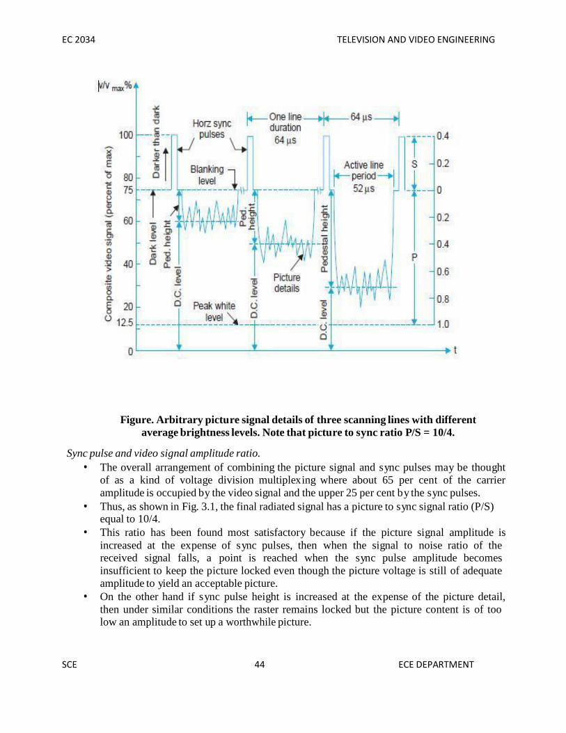
EC 2034 TELEVISION AND VIDEO ENGINEERING
SCE 4444
ECE DEPARTMENT
Figure. Arbitrary picture signal details of three scanning lines with differentaverage brightness levels. Note that picture to sync ratio P/S = 10/4.
Sync pulse and video signal amplitude ratio. The overall arrangement of combining the picture signal and sync pulses may be thought
of as a kind of voltage division multiplexing where about 65 per cent of the carrieramplitude is occupied by the video signal and the upper 25 per cent by the sync pulses.
Thus, as shown in Fig. 3.1, the final radiated signal has a picture to sync signal ratio (P/S)equal to 10/4.
This ratio has been found most satisfactory because if the picture signal amplitude isincreased at the expense of sync pulses, then when the signal to noise ratio of thereceived signal falls, a point is reached when the sync pulse amplitude becomesinsufficient to keep the picture locked even though the picture voltage is still of adequateamplitude to yield an acceptable picture.
On the other hand if sync pulse height is increased at the expense of the picture detail,then under similar conditions the raster remains locked but the picture content is of toolow an amplitude to set up a worthwhile picture.

EC 2034 TELEVISION AND VIDEO ENGINEERING
SCE 4545
ECE DEPARTMENT
A ratio of P/S = 10/4, or thereabout, results in a situation such that when the signal tonoise ratio reaches a certain low level, the sync amplitude becomes insufficient, i.e., thesync fails at the same time as the picture ceases to be of entertainment value. Thisrepresents the most efficient use of the television system
Figure. Horizontal and vertical blanking pulses in video signal. Sync pulses areadded above the blanking level and occupy upper 25% of the composite video signal
amplitude
1.15. HORIZONTAL SYNC DETAILSThe horizontal blanking period and sync pulse details are illustrated in Fig. The interval
between horizontal scanning lines is indicated by H. As explained earlier, out of a total lineperiod of 64s, the line blanking period is 12 s. During this interval a line synchronizing pulseis inserted. The pulses corresponding to the differentiated leading edges of the sync pulses areactually used to synchronize the horizontal scanning oscillator. This is the reason why in Figandother figures to follow, all time intervals are shown between sync pulse leading edges.The line blanking period is divided into three sections. These are the ‘front porch’, t he ‘line sync’pulse and the ‘back porch’. The time intervals allowed to each part are summarized below andtheir location and effect on the raster is illustrated in Fig.Details of Horizontal Scanning
Period Time (µs)Total line (H) 64Horz blanking 12 ± .3Horz sync pulse 4.7 ± 0.2Front porch 1.5 ± .3Back porch 5.8 ± .3Visible line time 52

EC 2034 TELEVISION AND VIDEO ENGINEERING
SCE 4646
ECE DEPARTMENT
Front porch. This is a brief cushioning period of 1.5 µ s inserted between the end of the picture detail
for that line and the leading edge of the line sync pulse. This interval allows the receivervideo circuit to settle down from whatever picture voltage level exists at the end of thepicture line to the blanking level before the sync pulse occurs.
Thus sync circuits at the receiver are isolated from the influence of end of the line picturedetails. The most stringent demand is made on the video circuits when peak white detailoccurs at the end of a line.
Despite the existence of the front porch when the line ends in an extreme white detail,and the signal amplitude touches almost zero level, the video voltage level fails to decayto the blanking level before the leading-edge of the line sync pulse occurs.
This results in late triggering of the time base circuit thus upsetting the ‘horz’ line synccircuit. As a result the spot (beam) is late in arriving at the left of the screen and pictureinformation on the next line is displaced to the left.
This effect is known as ‘pulling-on-whites’.Line sync pulse.
After the front proch of blanking, horizontal retrace is produced when the sync pulsestarts. The flyback is definitely blanked out because the sync level is blacker than black.
Line sync pulses are separated at the receiver and utilized to keep the receiver line timebase in precise synchronism with the distant transmitter.
The nominal time duration for the line sync pulses is 4.7s. During this period the beamon the raster almost completes its back stroke (retrace) and arrives at the extreme left endof the raster.
Back porch.
This period of 5.8 µ s at the blanking level allows plenty of time for line flyback to becompleted. It also permits time for the horizontal time-base circuit to reverse direction ofcurrent for the initiation of the scanning of next line.
In fact, the relative timings are so set that small black bars (see Fig) are formed at boththe ends of the raster in the horizontal plane.
These blanked bars at the sides have no effect on the picture details reproduced duringthe active line period.
The back porch also provides the necessary amplitude equal to the blanking level(reference level) and enables to preserve the dc content of the picture information at thetransmitter.
At the receiver this level which is independent of the picture details is utilized in theAGC (automatic gain control) circuits to develop true AGC voltage proportional to thesignal strength picked up at the antenna

EC 2034 TELEVISION AND VIDEO ENGINEERING
SCE 4747
ECE DEPARTMENT
1.16. VERTICAL SYNC DETAILS
The vertical sync pulse train added after each field is somewhat complex in nature. Thereason for this stems from the fact that it has to meet several exacting requirements.
Therefore, in order to fully appreciate the various constituents of the pulse train, thevertical sync details are explored step by step while explaining the need for its variouscomponents.
The basic vertical sync added at the end of both even add odd fields is shown in Fig. Itswidth has to be kept much larger than the horizontal sync pulse, in order to derive asuitable field sync pulse at the receiver to trigger the field sweep oscillator. The standardsspecify that the vertical sync period should be 2.5 to 3 times the horizontal line period. Ifthe width is less than this, it becomes difficult to distinguish between horizontal andvertical pulses at the receiver.
In color TV transmission a short sample (8 to 10 cycles) of the color subcarrier oscillatoroutput is sent to the receiver for proper detection of color signal sidebands.
This is known as color burst and is located at the back porch of the horizontal blankingpedestal. If the width is greater than this, the transmitter must operate at peak power foran unnecessarily long interval of time. In the 625 line system 2.5 line period (2.5 × 64 =160 µ s) has been allotted for the vertical sync pulses.

EC 2034 TELEVISION AND VIDEO ENGINEERING
SCE 4848
ECE DEPARTMENT
Thus a vertical sync pulse commences at the end of 1st half of 313th line (end of firstfield) and terminates at the end fo 315th line. Similarly after an exact interval of 20 ms(one field period) the next sync pulse occupies line numbers 1st, 2nd and 1st half of third,just after the second field is over.
Note that the beginning of these pulses has been aligned in the figure to signify that thesemust occur after the end of vertical stroke of the beam in each field, i.e., after each 1/50thof a second.
This alignment of vertical sync pulses, one at the end of a half-line period and the otherafter a full line period (see Fig.)results in a relative misalignment of the horizontal syncpulses and they do not appear one above the other but occur at half-line intervals withrespect to each other.
However, a detailed examination of the pulse trains in the two fields would show thathorizontal sync pulses continue to occur exactly at 64 µ s intervals (except during thevertical sync pulse periods) throughout the scanning period from frame to frame and theapparent shift of 32 µ s is only due to the alignment of vertical sync instances in thefigure.
As already mentioned the horizontal sync information is extracted from the sync pulsetrain by differentiation, i.e., by passing the pulse train through a high-pass filter. Indeedpulses corresponding to the differentiated leading edges of sync pulses are used tosynchronize the horizontal scanning oscillator.
The process of deriving these pulses is illustrated in Fig. Furthermore, receivers often usemono stable multi-vibrators to generate horizontal scan, andso a pulse is required toinitiate each and every cycle of the horizontal oscillator in the receiver. This brings outthe first and most obvious shortcoming of the waveforms shown in Fig.
Figure. Composite video waveforms showing horizontal and basic vertical sync pulses atthe end of (a) second (even) field, (b) first (odd) field. Note, the widths of horizontal
blanking intervals and sync pulses are exaggerated.

EC 2034 TELEVISION AND VIDEO ENGINEERING
SCE 4949
ECE DEPARTMENT
The horizontal sync pulses are available both during the active and blanked line periodsbut there are no sync pulses (leading edges) available during the 2.5 line vertical syncperiod.
Thus the horizontal sweep oscillator that operates at 15625 Hz, would tend to step out ofsynchronism during each vertical sync period. The situation after an odd field is evenworse.
As shown in Fig. the vertical blanking period at the end of an odd field begins midwaythrough a horizontal line. Consequently, looking further along this waveform, we see thatthe leading edge of the vertical sync pulse comes at the wrong time to providesynchronization for the horizontal oscillator.
Therefore, it becomes necessary to cut slots in the vertical sync pulse at half-line-intervals to provide horizontal sync pulses at the correct instances both after even and oddfields.
The technique is to take the video signal amplitude back to the blanking level 4.7 µ sbefore the line pulses are needed. The waveform is then returned back to the maximumlevel at the moment the line sweep circuit needs synchronization.
Thus five narrow slots of 4.7 µ s width get formed in each vertical sync pulse at intervalsof 32 µ s. The trailing but rising edges of these pulses are actually used to trigger thehorizontal oscillator.
The resulting waveforms together with line numbers and the differentiated output of boththe field trains is illustrated in Fig.
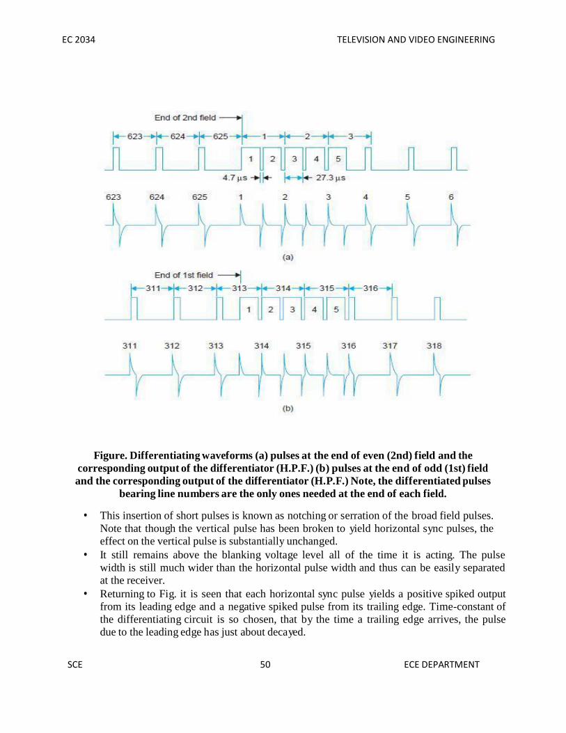
EC 2034 TELEVISION AND VIDEO ENGINEERING
SCE 5050
ECE DEPARTMENT
Figure. Differentiating waveforms (a) pulses at the end of even (2nd) field and thecorresponding output of the differentiator (H.P.F.) (b) pulses at the end of odd (1st) fieldand the corresponding output of the differentiator (H.P.F.) Note, the differentiated pulses
bearing line numbers are the only ones needed at the end of each field.
This insertion of short pulses is known as notching or serration of the broad field pulses.Note that though the vertical pulse has been broken to yield horizontal sync pulses, theeffect on the vertical pulse is substantially unchanged.
It still remains above the blanking voltage level all of the time it is acting. The pulsewidth is still much wider than the horizontal pulse width and thus can be easily separatedat the receiver.
Returning to Fig. it is seen that each horizontal sync pulse yields a positive spiked outputfrom its leading edge and a negative spiked pulse from its trailing edge. Time-constant ofthe differentiating circuit is so chosen, that by the time a trailing edge arrives, the pulsedue to the leading edge has just about decayed.

EC 2034 TELEVISION AND VIDEO ENGINEERING
SCE 5151
ECE DEPARTMENT
The negative-going triggering pulses may be removed with a diode since only thepositive going pulses are effective in locking the horizontal oscillator. However, thepulses actually utilized are the ones that occur sequentially at 64 µ s intervals. Such pulsesare marked with line numbers for both the fields. Note that during the intervals ofserrated vertical pulse trains, alternate vertical spikes are utilized.
The pulses not used in one field are the ones utilized during the second field. Thishappens because of the half-line difference at the commencement of each field and thefact that notched vertical sync pulses occur at intervals of 32 µ s and not 64 µ s as requiredby the horizontal sweep oscillator.
The pulses that come at a time when they cannot trigger the oscillator are ignored. Thusthe requirement of keeping the horizontal sweep circuit locked despite insertion ofvertical sync pulses is realized.
Now we turn to the second shortcoming of the waveform of Fig. First it must bementioned that synchronization of the vertical sweep oscillator in the receiver is obtainedfrom vertical sync pulses by integration.
This is illustrated in Fig. where the time-constant R2C2 is chosen to be large compared tothe duration of horizontal pulses but not with respect to width of the vertical sync pulses.
The integrating circuit may equally be looked upon as a low pass filter, with a cut-offfrequency such that the horizontal sync pulses produce very little output, while thevertical pulses have a frequency that falls in the pass-band of the filter.
The voltage built across the capacitor of the low-pass filter (integrating circuit)corresponding to the sync pulse trains of both the fields is shown in Fig. Note that eachhorizontal pulse causes a slight rise in voltage across the capacitor but this is reduced tozero by the time the next pulse arrives.
This is so, because the charging period for the capacitor is only 4.7 µ s and the voltage atthe input to the integrator remains at zero for the rest of the period of 59.3 µ s.
Hence there is no residual voltage across the vertical filter (L.P. filter) due to horizontalsync pulses. Once the broad serrated vertical pulse arrives the voltage across the output ofthe filter starts increasing. However, the built up voltage differs for each field.
The reason is not difficult to find. At the beginning of the first field (odd field) the lasthorz sync pulse corresponding to the beginning of 625th line is separated from the 1stvertical pulse by full one line and any voltage developed across the filter will haveenough time to return to zero before the arrival of the first vertical pulse, and thus thefilter output voltage builds up from zero in response to the five successive broad verticalsync pulses.
The voltage builds up because the capacitor has more time to charge and only 4.7 µ s todischarge. The situation, however, is not the same for the beginning of the 2nd (even)field. Here the last horizontal pulse corresponding to the beginning of 313th line isseparated from the first vertical pulse by only half-a-line.
The voltage developed across the vertical filter will thus not have enough time to reachzero before the arrival of the first vertical pulse, which means that the voltage build-updoes not start from zero, as in the case of the 1st field. The residual voltage on account ofthe half line discrepancy gets added to the voltage developed on account of the broad

EC 2034 TELEVISION AND VIDEO ENGINEERING
SCE 5252
ECE DEPARTMENT
vertical pulses and thus the voltage developed across the output filter is some what higherat each instant as compared to the voltage developed at the beginning of the first-field.
This is shown in dotted chain line in Fig. The vertical oscillator trigger potential levelmarked as trigger level in the diagram (Fig. )intersects the two filter output profiles atdifferent points which indicates that in the case of second field the oscillator will gettriggered a fraction of a second too soon as compared to the first field. Note that thisinequality in potential levels for the two fields continues during the period of discharge ofthe capacitor once the vertical sync pulses are over and the horizontal sync pulses take-over.
Though the actual time difference is quite short it does prove sufficient to upset thedesired interlacing sequence. End of 2nd field 1st field Equalizing pulses. To take care ofthis drawback which occurs on account of the half-a-line discrepancy five narrow pulsesare added on either side of the vertical sync pulses.
These are known as pre-equalizing and post-equalizing pulses. Each set consists of fivenarrow pulses occupying 2.5 lines period on either side of the vertical sync pulses. Pre-equalizing and post equalizing pulse details with line numbers occupied by them in eachfield are given in Fig.
The effect of these pulses is to shift the half-line discrepancy away both from thebeginning and end of vertical sync pulses. Pre-equalizing pulses being of 2.3 µ s durationresult in the discharge of the capacitor to essentially zero voltage in both the fields,despite the half-line discrepancy before the voltage build-up starts with the arrival ofvertical sync pulses.
This is illustrated in Fig. Post-equalizing pulses are necessary for a fast discharge of thecapacitor to ensure triggering of the vertical oscillator at proper time. If the decay ofvoltage across the capacitor is slow as would happen in the absence of post-equalizingpulses, the oscillator may trigger at the trailing edge which may be far-away from theleading edge and this could lead to an error in triggering.
Thus with the insertion of narrow pre and post equalizing pulses, the voltage rise and fallprofile is essentially the same for both the field sequences (see Fig.) and the verticaloscillator is triggered at the proper instants, i.e., exactly at an interval of 1/50th of asecond.
This problem could possibly also be solved by using an integrating circuit with a muchlarger time constant, to ensure that the capacitor remains virtually uncharged by thehorizontal pulses. However, this would have the effect of significantly reducing theintegrator output for vertical pulses so that a vertical sync amplifier would have to beused.
In a broadcasting situation, there are thousands of receivers for every transmitter.Consequently it is much more efficient and economical to cure this problem in onetransmitter than in thousands of receivers. This, as explained above, is achieved by theuse of pre and post equalizing pulses.
The complete pulse trains for both the fields incorporating equalizing pulses are shown in.From the comparison of the horizontal and vertical output pulse forms shown in Fig andit appears that the vertical trigger pulse (output of the low-pass filter) is not very sharpbut actually it is not so. The scale hosen exaggerates the extent of the vertical pulses. Thevoltage build-up period is only 160 µ s and so far as the vertical synchronizing oscillator

EC 2034 TELEVISION AND VIDEO ENGINEERING
SCE 5353
ECE DEPARTMENT
is concerned this pulse occurs rapidly and represents a sudden change in voltage whichdecays very fast.
The polarity of the pulses as obtained at the outputs of their respective fields may not besuitable for direct application in the controlled synchronizing oscillator and might needinversion.
Figure. Integrating waveforms (a) pulses at the end of 2nd (even) field (b) pulses at the endof 1st (odd) field (c) integrator output. Note the above sync pulses have purposely been
drawn without equalizing pulses

EC 2034 TELEVISION AND VIDEO ENGINEERING
SCE 5454
ECE DEPARTMENT
Figure. Pre-sync equalizing and Post-sync equalizing pulses.

EC 2034 TELEVISION AND VIDEO ENGINEERING
SCE 5555
ECE DEPARTMENT
313th 2nd-half, 314, 315 2.5 lines316, 317, 318th 1st-half 2.5 lines
——
Vertical sync pulsesPost-vertical sync equalizing pulses
318th 2nd-half-to 330 12.5 lines — Blanking retrace pulses331 to 1st-half of 623rd 292.5 line — Picture details623 2nd-half, 624 and 625 2.5 lines — Pre-vertical sync equalizing pulses for the
1st fieldTotal number of lines = 312.5Total Number of Lines per Frame = 625
Figure. Identical vertical sync voltage built-up across the integrating capacitor.
1.17. SCANNING SEQUENCE DETAILS A complete chart giving line numbers and pulse designations for both the fields
(corresponding to Fig) is given below :First Field (odd field)Line numbers : one to 1st-half of 313th line (312.5 lines)1, 2 and 3rd 1st-half, lines 2.5 lines — Vertical sync pulses3rd 2nd-half, 4, and 5 2.5 lines — Post-vertical sync equalizing pulses.6 to 17, and 18th 1st-half 12.5 lines — blanking retrace pulses18th 2nd-half to 310 292.5 lines — Picture details311, 312, and 313th 1st-half 2.5 lines— Pre-vertical sync equalizing pulses for the 2nd field.Total number of lines = 312.5Second field (even field)Line numbers : 313th 2nd-half to 625 (312.5 lines)

EC 2034 TELEVISION AND VIDEO ENGINEERING
SCE 5656
ECE DEPARTMENT
Figure. Field synchronizing pulse trains of the 625 lines TV system.
COMPOSITE VIDEO SIGNAL
Approximate location of line numbers. The serrated vertical sync pulse forces the verticaldeflection circuity to start the flyback. However, the flyback generally does not beginwith the start of vertical sync because the sync pulse must build up a minimum voltageacross the capacitor to trigger the scanning oscillator.
If it is assumed that vertical flyback starts with the leading edge of the fourth serration, atime of 1.5 lines passes during vertical sync before vertical flyback starts. Also fiveequalizing pulses occur before vertical sync pulse train starts.
Then four lines (2.5 + 1.5 = 4) are blanked at the bottom of the pricture before verticalretrace begins. A typical vertical retrace time is five lines. Thus the remaining eleven (20– (4 + 5) =11) lines are blanked at the top of the raster. These lines provide the sweep

EC 2034 TELEVISION AND VIDEO ENGINEERING
SCE 5757
ECE DEPARTMENT
oscillator enough time to adjust to a linear rise for uniform pick-up and reproduction ofthe picture.
FUNCTIONS OF VERTICAL PULSE TRAIN By serrating the vertical sync pulses and the providing pre- and post-equalizing
pulses the following basic requirements necessary for successful interlacedscanning are ensured.
(a) A suitable field sync pulse is derived for triggering the field oscillator.(b) The line oscillator continues to receive triggering pulses at correct intervals while theprocess of initiation and completion of the field time-base stroke is going on.(c) It becomes possible to insert vertical sync pulses at the end of a line after the 2nd field and atthe middle of a line at the end of the 1st field without causing any interlace error.(d) The vertical sync build up at the receiver has precisely the same shape and timing onodd and even fields.
PREFERENCE OF AM FOR PICTURE SIGNAL TRANSMISSION At the VHF and UHF carrier frequencies there is a displacement in time between
the direct and reflected signals. The distortion which arises due to interferencebetween multiple signals is more objectionable in FM than AM because fhefrequency of the FM signal continuously changes.
If FM were used for picture transmission, the changing best frequency betweenthe multiple paths, delayed with respect to each other, would produce a barinterference pattern in the image with a shimmering effect, since the barscontinuously change as the beat frequency
POSITIVE AND NEGATIVE MODULATION
When the intensity of picture brightness causes increase in amplitude of the modulatedenvelope,it is called ‘positive’ modulation.
When the polarity of modulating video signal is so chosen that sync tips lie at the 100 percent level of carrier amplitude and increasing brightness produces decrease in themodulation envelope, it is called ‘negative modulation’.
The two polarities of modulation are illustrated in Fig

EC 2034 TELEVISION AND VIDEO ENGINEERING
SCE 5858
ECE DEPARTMENT
Figure. RF waveforms of an amplitude modulated composite video signal.
Comparison of Positive and Negative Modulation Effect of Noise Interference on Picture Signal. Noise pulses created by automobile
ignition systems are most troublesome. The RF energy contained in such pulses is spreadmore or less uniformly over a wide frequency range and has a random distribution ofphase and amplitude.
When such RF pulses are added to sidebands of the desired signal, and sum of signal andnoise is demodulated, the demodulated video signal contains pulses corresponding to RFnoise peaks, which extend principally in the direction of increasing envelope amplitude.This is shown in Fig.
Thus in negative system of modulation, noise pulse extends in black direction of thesignal when they occur during the active scanning intervals. They extend in the directionof sync pulses when they occur during blanking intervals. In the positive system, thenoise extends in the direction of the white during active scanning, i.e., in the oppositedirection from the sync pulse during blanking.
Obviously the effect of noise on the picture itself is less pronounced when negativemodulation is used. With positive modulation noise pulses will produce white blobs onthe screen whereas in negative modulation the noise pulses would tend to produce blackspots which are less noticeable against a grey background.
This merit of lesser noise interference on picture information with negative modulationhas led to its use in most TV systems. (b) Effect of Noise Interference onSynchronization. Sync pulses with positive modulation being at a lesser level of themodulated carrier envelope are not much affected by noise pulses.
However, in the case of negatively modulated signal, it is sync pulses which exist atmaximum carrier amplitude, and the effect of interference is both to mutilate some of

EC 2034 TELEVISION AND VIDEO ENGINEERING
these, and to produce lot of spurious random pulses. This can completely upset thesynchronization of the receiver time bases unless something is done about it.
Because of almost universal use of negative modulation, special horizontal stabilizingcircuits have been developed for use in receivers to overcome the adverse effect of noiseon synchronization. (c) Peak Power Available from the Transmitter. With positivemodulation, signal corresponding to white has maximum carrier amplitude.
The RF modulator cannot be driven harder to extract more power because the non-lineardistortion thus introduced would affect the amplitude scale of the picture signal andintroduce brightness distortion in very bright areas of the picture.
In negative modulation, the transmitter may be over-modulated during the sync pulseswithout adverse effects, since the non-linear distortion thereby introduced, does not verymuch affect the shape of sync pulses. Consequently, the negative polarity of modulationpermits a large increase in peak power output and for a given setup in the final transmitterstage the output increases by about 40%. (d) Use of AGC (Automatic Gain Control)Circuits in the Receiver.
Most AGC circuits in receivers measure the peak level of the incoming carrier signal andadjust the gain of the RF and IF amplifiers accordingly. To perform this measurementsimply, a stable reference level must be available in the signal. In negative system ofmodulation, such a level is the peak of sync pulses which remains fixed at 100 per cent ofsignal amplitude and is not affected by picture details.
This level may be selected simply by passing the composite video signal through a peakdetector. In the positive system of modulation the corresponding stable level is zeroamplitude at the carrier and obviously zero is no reference, and it has no relation to thesignal strength.
The maximum carrier amplitude in this case depends not only on the strength of thesignal but also on the nature of picture modulation and hence cannot be utilized todevelop true AGC voltage. Accordingly AGC circuits for positive modulation must selectsome other level (blanking level) and this being at low amplitude needs elaboratecircuitry in the receiver.
Thus negative modulation has a definite advantage over positive modulation in thisrespect. The merits of negative modulation over positive modulation, so far as picturesignal distortion and AGC voltage source are concerned, have led to the use of negativemodulation in almost all TV systems now in use.
SCE 59 ECE DEPARTMENT
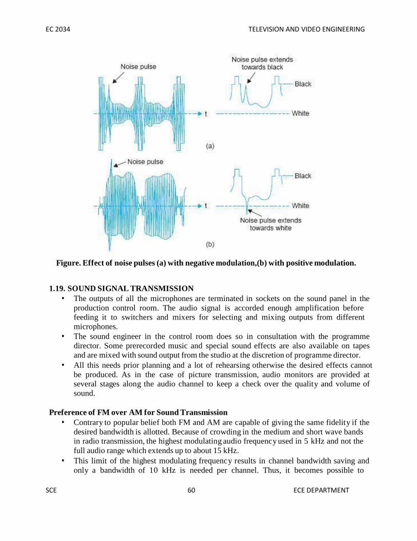
EC 2034 TELEVISION AND VIDEO ENGINEERING
Figure. Effect of noise pulses (a) with negative modulation,(b) with positive modulation.
1.19. SOUND SIGNAL TRANSMISSION The outputs of all the microphones are terminated in sockets on the sound panel in the
production control room. The audio signal is accorded enough amplification beforefeeding it to switchers and mixers for selecting and mixing outputs from differentmicrophones.
The sound engineer in the control room does so in consultation with the programmedirector. Some prerecorded music and special sound effects are also available on tapesand are mixed with sound output from the studio at the discretion of programme director.
All this needs prior planning and a lot of rehearsing otherwise the desired effects cannotbe produced. As in the case of picture transmission, audio monitors are provided atseveral stages along the audio channel to keep a check over the quality and volume ofsound.
Preference of FM over AM for Sound Transmission Contrary to popular belief both FM and AM are capable of giving the same fidelity if the
desired bandwidth is allotted. Because of crowding in the medium and short wave bandsin radio transmission, the highest modulating audio frequency used in 5 kHz and not thefull audio range which extends up to about 15 kHz.
This limit of the highest modulating frequency results in channel bandwidth saving andonly a bandwidth of 10 kHz is needed per channel. Thus, it becomes possible to
SCE 60 ECE DEPARTMENT

EC 2034 TELEVISION AND VIDEO ENGINEERING
accommodate a large number of radio broadcast stations in the limited broadcast band.Since most of the sound signal energy is limited to lower audio frequencies, the soundreproduction is quite satisfactory.
Frequency modulation, that is capable of providing almost noise free and high fidelityoutput needs a wider swing in frequency on either side of the carrier. This can be easilyallowed in a TV channel, where, because of very high video frequencies a channelbandwidth of 7 MHz is allotted. In FM, where highest audio frequency allowed is 15kHz, the sideband frequencies do not extend too far and can be easily accommodatedaround the sound carrier that lies 5.5 MHz awayfrom the picture carrier.
The bandwidth assigned to the FM sound signal is about 200 kHz of which not more than100 kHz is occupied by sidebands of significant amplitude. The latter figure is only 1.4per cent of the total channel bandwidth of 7 MHz. Thus, without encroaching much, in arelative sense, on the available band space for television transmission all the advantagesof FM can be availed.
SCE 61 ECE DEPARTMENT

EC 2034 TELEVISION AND VIDEO ENGINEERING
SCE 6262
ECE DEPARTMENT
UNIT II
MONOCHROME TELEVISION TRANSMITTER AND RECEIVER
2.1. TELEVISION TRANSMITTER
A simplified functional block diagram of a television transmitter is shown in Fig.Necessary details of video signal modulation with picture carrier of allotted channel areshown in picture transmitter section of the diagram. Note the inclusion of a dc restorercircuit (DC clamp) before the modulator.
Also note that because of modulation at a relatively low power level, an amplifier is usedafter the modulated RF amplifier to raise the power level.
Accordingly this amplifier must be a class-B push-pull linear RF amplifier. Both themodulator and power amplifier sections of the transmitter employ specially designed VHFtriodes for VHF channels and klystrons in transmitters that operate in UHF channels.
Vestigial Sideband Filter
The modulated output is fed to a filter designed to filter out part of the lower sidebandfrequencies. As already explained this results in saving of band space.
Antenna
The filter output feeds into a combining network where the output from the FM soundtransmitter is added to it.
This network is designed in such a way that while combining, either signal does notinterfere with the working of the other transmitter.
A coaxial cable connects the combined output to the antenna system mounted on a hightower situated close to the transmitter.
A turnstile antenna array is used to radiate equal power in all directions. The antenna ismounted horizontally for better signal to noise ratio

EC 2034 TELEVISION AND VIDEO ENGINEERING
SCE 6363
ECE DEPARTMENT
Figure. Simplified block diagram of a television transmitter.
2.4. TELEVISION TRANSMISSION ANTENNAS
As already explained, television signals are transmitted by space wave propagation and sothe height of antenna must be as high as possible in order to increase the line-of-sightdistance.
Horizontal polarization is standard for television broadcasting, as signal to noise ratio isfavorable for horizontally polarized waves when antennas are placed quite high above thesurface of the earth.

EC 2034 TELEVISION AND VIDEO ENGINEERING
SCE 6464
ECE DEPARTMENT
Turnstile Array
Figure. Turnstile array.
To obtain an omnidirectional radiation pattern in the horizontal plane, for equal televisionsignal radiation in all directions, an arrangement known as ‘turnstile array’ is often used.
In this type of antenna two crossed dipoles are used in a turnstile arrangement as shown inFig. These are fed in quadrature from the same source by means of an extra λ/4 line. Eachdipole has a figure of eight pattern in the horizontal plane, but crossed with each other. Theresultant field in all directions is equal to the square root of the sum of the squares of fieldsradiated by each conductor in that direction.
Thus the resultant pattern as shown in Fig. is very nearly circular in the plane of the turnstileantenna. Fig. shows several turnstiles stacked one above the other for vertical directivity.
Figure. Directional pattern in the plane of turnstile.

EC 2034 TELEVISION AND VIDEO ENGINEERING
SCE 6565
ECE DEPARTMENT
Figure. Stacked turnstile array.
Dipole Panel Antenna System
Another antenna system that is often used for band I and band III transmitters consists ofdipole panels mounted on the four sides at the top of the antenna tower as shown in Fig.
Each panel consists of an array of full-wave dipoles mounted in front of reflectors. Forobtaining unidirectional pattern the four panels mounted on the four sides of the tower areso fed that the current in each lags behind the previous by 90°.
This is achieved by varying the field cable length by λ/4 to the two alternate panels and byreversal of polarity of the current.

EC 2034 TELEVISION AND VIDEO ENGINEERING
SCE 6666
ECE DEPARTMENT
Figure. Dipole panel antenna system (a) panel of dipoles (b) radiation pattern of four towermounted dipole antenna panels.
Combining Network
The AM picture signal and FM sound signal from the corresponding transmitters are fedto the same antenna through a balancing unit called diplexer.
As illustrated in Fig. the antenna combining system is a bridge configuration in which firsttwo arms are formed by the two radiators of the turnstile antenna and the other two armsconsist of two capacitive reactance.
Under balanced conditions, video and sound signals though radiated by the same antenna,do not interfere with the functioning of the transmitter other than their own.
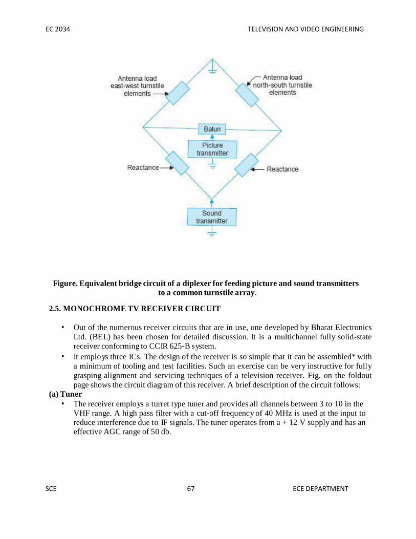
EC 2034 TELEVISION AND VIDEO ENGINEERING
SCE 6767
ECE DEPARTMENT
Figure. Equivalent bridge circuit of a diplexer for feeding picture and sound transmittersto a common turnstile array.
2.5. MONOCHROME TV RECEIVER CIRCUIT
Out of the numerous receiver circuits that are in use, one developed by Bharat ElectronicsLtd. (BEL) has been chosen for detailed discussion. It is a multichannel fully solid-statereceiver conforming to CCIR 625-B system.
It employs three ICs. The design of the receiver is so simple that it can be assembled* witha minimum of tooling and test facilities. Such an exercise can be very instructive for fullygrasping alignment and servicing techniques of a television receiver. Fig. on the foldoutpage shows the circuit diagram of this receiver. A brief description of the circuit follows:
(a) Tuner The receiver employs a turret type tuner and provides all channels between 3 to 10 in the
VHF range. A high pass filter with a cut-off frequency of 40 MHz is used at the input toreduce interference due to IF signals. The tuner operates from a + 12 V supply and has aneffective AGC range of 50 db.

EC 2034 TELEVISION AND VIDEO ENGINEERING
SCE 6868
ECE DEPARTMENT
(b) Video IF Section
The video IF sub-system consists of IC, BEL CA**3068 and other associated componentshoused in a modular box to avoid any possible RF interference.
All interconnections to this module are *The technical manual of the receiver can beobtained on request from M/s Bharat Electronics Ltd. Jalahalli, P.O., Bangalore 560013India.
The manual gives all necessary circuit details, coil data, list of components, assembly andalignment details. either through feed through capacitors or insulated lead throughs.
The IF sub-assembly provides (i) a gain around 75 db to the incoming signal from the tuner,(ii) required selectivity and bandwidth, (iii) attenuation to adjacent channel interferingfrequencies, (iv) attenuation of 26 db to sound IF for intercarrier sound, (v) sound IF andvideo outputs and (vi) AGC voltage to the IF section and tuner.
(c) Sound IF Sub-system and Audio Section
The important functions performed by this sub-system are:(i) to amplify inter carrier IF signal available from the picture IF amplifier,(ii) to recover sound signal,(iii) to amplify the sound signal and deliver at least 2 watts of audio power to the
loudspeaker.The circuit of BEL CA*3065 IC consists of
(i) a regulated power supply,(ii) a sound IF amplifier-limiter,(iii) an FM limiter,(iv) an electronic attenuator and a buffer amplifier, and(v) an audio driver.
The sound section operates from a + 12 V supply. It employs transistor BC 148B as a boot-strapped driver and matched transistor pair, 2N5296 and 2N6110, at the output stage. Thebandwidth of the audio amplifier is from 40 Hz to 15 KHz and can deliver 2 watts of usefulaudio power.
(d) Video Amplifier and Picture Tube Biasing
This section of the receiver uses transistors BF 195 C as driver (buffer), BD115 as videoamplifier and BC147B in the blanking circuit. The video amplifier delivers 90 V p-p signalto the cathode of picture tube 500-C1P4.
The current limiting is provided by diode 0A79 and associated circuitry. Transistor Q 503switches amplifier transistor Q502 only during the time when video signal is present andturns it off during horizontal and vertical sync periods.
The horizontal blanking pulses of 60 V p-p and vertical blanking pulses of 40 V p-p areapplied to the base of transistor Q503. High voltage output of 1.1 KV from the horizontaloutput circuit is rectified and fed to focusing grids of the picture tube through a potential

EC 2034 TELEVISION AND VIDEO ENGINEERING
SCE 6969
ECE DEPARTMENT
divider. Brightness control operates from a + 200 V supply. The contrast control functionsby varying input signal amplified to the video amplifier transistor Q 502.
(e) Horizontal Oscillator Sub-system
This section employs transistor Q 401 (BC 148 A), IC, CA 920 and associated passivecomponents. Composite video signal from the IF section is applied to pin 8 of IC 401 (CA920). The functions of the horizontal subsystem are:
(i) To generate a line frequency signal, the frequency of which can be current controlled,(ii) To separate sync information from the composite signal,(iii) To compare the phase of sync pulses with that of the oscillator output and generate a
control voltage for automatic tuning of the oscillator.(iv) Phase comparison between the oscillator waveform and middle of the line flyback Pulse,
to generate a control voltage for correction of the switching delay time in the horizontal drivingand output stages, and
(v) Shaping and amplification of the oscillator output to obtain pulses capable of driving thehorizontal deflection driver circuit.(f) Horizontal Output Circuit
Output from the horizontal oscillator is applied to the base of horizontal driver transistorQ802 through a coupling capacitor (C 803). The transistor switches from cut-off tosaturation when a pulse is applied to its base and provides the necessary drive for Q803(BU 205).
The output transistor (Q803) drives the line output transformer to provide deflectioncurrent to the yoke coils. In addition, the output circuit (i) generates flyback pulses forblanking, AFC and AGC keying, (ii) provides auxiliary power supplies and generates highvoltage (+ 18 KV) for anode of the picture tube and (iii) produces 1.1 KV dc for thefocusing grids. The heater supply of 6.3 V for the picture tube is taken across winding 10-11 of the line output transformer.
(g) Vertical Deflection Circuit
As shown in Fig. 29.1, the circuit operates from a 40 V dc supply obtained through the lineoutput transformer. This sub-system is a self-oscillatory synchronized oscillator with amatched pair of output transistors.
Clipped vertical sync pulses are fed at the base of Q 70 (BC 148 C) to provide it with astable drive. Resistor R 724 senses yoke current and feeds a voltage proportional to thiscurrent back to the base of Q 702 (BC148 B) for adjustment of the picture height. Couplingnetwork between the collector of Q 701 and the base of Q 702 incorporates the necessary‘S’ correction and provides linearity of the deflection current. Hold control forms part ofthe input circuit of transistor Q 701.
(h) Power Supply Circuit
The power supply circuit is a conventional transformerless half-wave rectifier and filtercircuit.

EC 2034 TELEVISION AND VIDEO ENGINEERING
SCE 7070
ECE DEPARTMENT
It provides 200 V for feeding various sections of the receiver. Front panel control. Fourcontrols i.e. on/off volume control, channel selector and fine tuning, contrast control andbrightness control are brought out at the front panel of the receiver.
In addition, vertical hold and horizontal hold controls are available on the side panel foroccasional adjustments.
2.6. RF TUNER
The RF amplifier, the local oscillator and the mixer stages form the RF tuning section. Thisis commonly known as ‘Tuner’ or ‘Front end’.
A simplified block diagram of the tuner is shown in Fig. It is the same for both monochromeand colour receivers except that automatic frequency tuning is provided in colour receiversonly.
The function of the tuner is to select a single channel signal from the many signals pickedup by the antenna, amplify it and mix it with the CW (continuous wave) output of the localoscillator to convert the channel frequencies to a band around the intermediate frequencyof the receiver.
It is the local oscillator that tunes in the desired station. Its frequency is unique for eachchannel, which determines the RF signal frequencies to be received and converted tofrequencies in the pass-band of the IF section.
TUNER OPERATION
As shown in the tuner block diagram the function of channel selection is accomplished bysimultaneously adjusting the tuned circuits of all the three stages that make up the tuner.This means that three or four tuned circuits must be switched while changing channels. Thetuned circuits found in both vacuum tube and transistor tuners are as follows:
(i) Input tuned circuit to the RF amplifier(ii) Output tuned circuit of the RF amplifier(iii) Input tuned circuit to the mixer(iv) Local oscillator tuned circuit
In some tuners the mixer input tuned circuit is left out and thus they have only three tunedcircuits. Each tuned circuit consists of a coil and a capacitor. The resonating capacitanceconsists of distributed capacitance of the circuit plus small fixed ceramic capacitors.
The fine tuning control is varied to obtain exact picture and sound intermediate frequenciesfor which the receiver is designed. The correct setting of the local oscillator frequency isindicated by the best picture obtained on the screen.
Physically, the tuner is wired as a sub-assembly on a separate chassis which is mounted onthe main receiver chassis. The IF signal from the tuner is coupled to the first picture IF

EC 2034 TELEVISION AND VIDEO ENGINEERING
SCE 7171
ECE DEPARTMENT
amplifier through a short coaxial cable. The AGC line and B+ supply are connected fromthe main chassis to the tuner sub chassis.
The tuner is enclosed in a compact shielded box and all connections are usually broughtout at the top of the tuner via feed through capacitors. In tube-type receivers, the filamentpower to the tuner tubes is also supplied from the common power supply.
Though the principle of selection in television receivers is the same as that in radioreceivers the design of the tuner is very different from the heterodyning section of the radioreceiver.
This is because of large band width requirements and very high frequencies employed forTV transmission. In fact tuner design techniques differ so much at ultra-high frequenciesthat all true multichannel receivers employ separate tuners for the VHF and UHF channels.We will confine our discussion to channels with frequencies 47 to 223 MHz in the VHFband (30 to 300 MHz).
Figure. Block diagram of a VHF tuner. Note that AFT is provided in colour receivers only.
FACTORS AFFECTING TUNER DESIGNThe factors that must be considered before attempting to learn details of the tuner circuitry
are:(a) Choice of IF and Local Oscillator Frequencies
(i) high image rejection ratio,(ii) reduced local oscillator radiation,(iii) ease of detection and(iv) good selectivity at the IF stages.
The local oscillator frequency is kept higher than the channel carrier frequency since thisresults in a relatively narrow oscillator frequency range.
It is then easier to design an oscillator that is stable and delivers almost constant outputvoltage over its entire frequency range. Intermediate frequencies have been standardized

EC 2034 TELEVISION AND VIDEO ENGINEERING
SCE 7272
ECE DEPARTMENT
in accordance with the total bandwidth allotted to each channel in different TV systems. Inthe 625-B monochrome system, the picture IF = 38.9 MHz and sound IF = 33.4 MHz.
(b) Need for an RF Amplifier Stage In principle an RF amplifier is not necessary and the signal could be fed directly to the
tuned input circuit of the mixer as is the normal practice in radio receivers. However, at very high frequencies the problems of image signals, radiation from the local
oscillator through the antenna circuit and conversion loss at the mixer are such that a stageof amplification prior to the mixer is desirable.
Another very important purpose of providing one stage of amplification is to feed enoughRF signal into the mixer for a clean picture without snow.
White speckles called snow are caused by excessive noise signals present in the videosignal. The mixer circuit generates most of the noise because of heterodyning.
Except in areas very close to the transmitter the signal level is moderate and a low noiseRF amplifier stage with a gain of about 25 db becomes necessary to obtain the desiredsignal-to-noise ratio of 30 : 1.
In fringe areas where the signal level is very low an additional RF amplifier known asbooster is often employed to maintain a reasonable signal-to-noise ratio. In all tunerdesigns the gain of the RF amplifier is controlled by AGC voltage to counter any variationsin the input signal to the receiver. A signal level of about 400 µ V at the input to the receiveris considered adequate for a snow free picture.
(c) Coupling Networks
Parallel tuned networks are used to accomplish the desired selectivity in RF and IF sectionsof the receiver. For minimum power loss the coupling network should match the outputimpedance of one stage to the input impedance of the following stage.
In circuits employing tubes this does not present any problem because the output and inputimpedance levels are not very different and the main criterion is to transfer maximumvoltage to the next stage.
However, in transistor amplifiers, where the input circuit also consume power, the interstage coupling network must be designed to transfer maximum power from the output ofone stage to the input of the following stage.
The coupling design is further complicated by the fact that in transistors the output andinput impedance levels are much different from each other. For example the inputimpedance of a common base configuration at very high frequencies is only a few tens ofohms, whereas its output impedance is of the order of several tens of kilo-ohms.

EC 2034 TELEVISION AND VIDEO ENGINEERING
SCE 7373
ECE DEPARTMENT
UHF TUNERS
There are two types of UHF tuners. In one type the converter section of the UHF tunerconverts the incoming signals from the UHF band (470 to 890 MHz) to the VHF band.Usually the UHF channels are converted to VHF channel numbers 5 or 6 and the VHFtuner, in turn, processes these signals in the usual way.
Since the relative positions of video and sound IFs are specified, the converter oscillator ofthe UHF tuner is tuned to a frequency lower than the incoming UHF signal to take intoaccount the double-heterodyning action involved. In the second type, the UHF signal isheterodyned with local oscillator output to translate the incoming channel directly to theIF band.
The output thus obtained from the UHF tuner is coupled to the VHF tuner, where the RFamplifier and mixer stages operate as IF amplifiers, when the VHF station selector is set tothe UHF position. In this position the VHF oscillator is disabled by cutting off its dc supply.The RF tuned circuits are also changed to IF tuned circuits. In present day tuners, this typeis preferred. Figure illustrates the block schematic of this circuit. Separate antennas areused for VHF and UHF channels.
The UHF tuner does not employ an RF amplifier because the input signal strength beingvery low is comparable to the noise generated in the RF amplifier. If used it lowers thesignal-to-noise ratio and fails to boost the signal level above the noise level.
Therefore, the incoming UHF signal is directly coupled to the mixer where a diode is usedfor heterodyning instead of a transistor or a special tube. The reason for using a diode istwo-fold. Firstly, the local oscillator output at ultrahigh frequencies is too low to causeeffective mixing with an active device whereas it is adequate when a diode is employed.Secondly the noise level with a diode is lower than when an active device is used. Sincethe diode is a non-linear device it can produce beating of the incoming channel frequencieswith the local oscillator frequency to generate side-band frequencies.
Block diagram of a UHF-VHF tuner
Figure. Block diagram of a UHF-VHF tuner

EC 2034 TELEVISION AND VIDEO ENGINEERING
SCE 7474
ECE DEPARTMENT
The weak output from the UHF tuner is coupled to the VHF tuner where both the RFamplifier and mixer stages acts as IF amplifiers to boost the signal to the level normallyobtained when a VHF channel is tuned.
In conclusion the various functions performed by a television receiver tuner may besummarized as follows:1. It selects the desired station and rejects others.2. It converts all incoming channel frequencies to a common IF band.3. It provides gain to the weak input signal picked up by the antenna. This improvesS/N ratio and reduces snow on the picture.4. It isolates the local oscillator from the feeder circuit to prevent undesired radiationthrough the antenna.5. It improves image rejection ratio and thus reduces interference from source operatingat frequencies close to the image frequencies of various channels.6. It prevents spurious pick-ups from sources which operate in the IF band of the receiver.7. It provides matching between the antenna and input circuits of the receiver, thuseliminating the appearance of ghost images on the screen.8. It rejects any pick-up from stations operating in the FM band.9. It has provision to select any channel out of the various allotted in the VHF and UHFbands for TV transmission.10. It has a fine tuning control for accurate setting of the selected station.
2.8. AUTOMATIC FINE TUNING (AFT)
The local oscillator frequency in the RF tuner is set to provide exact IF frequencies.However, despite many remedial measures to improve the stability of the oscillator circuit,some drift does occur on account of ambient temperature changes, component aging, andpower supply voltage fluctuations and so on.
For a monochrome receiver a moderate amount of change in the local oscillator frequencycan be tolerated without much effect on the reproduced picture and sound output. The finetuning control is adjusted occasionally to get a sharp picture. The sound output isautomatically corrected because of the use of inter carrier sound system. However,requirements of frequency stability of the local oscillator in a colour TV receiver are muchmore stringent.
This is so, because proper fine tuning of colour receivers is judged both by the sharpnessof the picture and quality of colour. If the local oscillator frequency becomes higher thanthe correct value, the picture IF, subcarrier IF and sound IF frequencies will also becomehigher by the same amount and fall on incorrect positions on the IF response curve.
This will result in poor picture quality because the amplitudes of low-frequency videosidebands clustered around the picture IF will decrease. At the same time chrominancesignal sidebands clustered around the location of subcarrier will receive more gain andhence become stronger than normal.
Similarly, if the local oscillator frequency changes to become less than the desired valueopposite effects would result and colour reproduction will become weak.
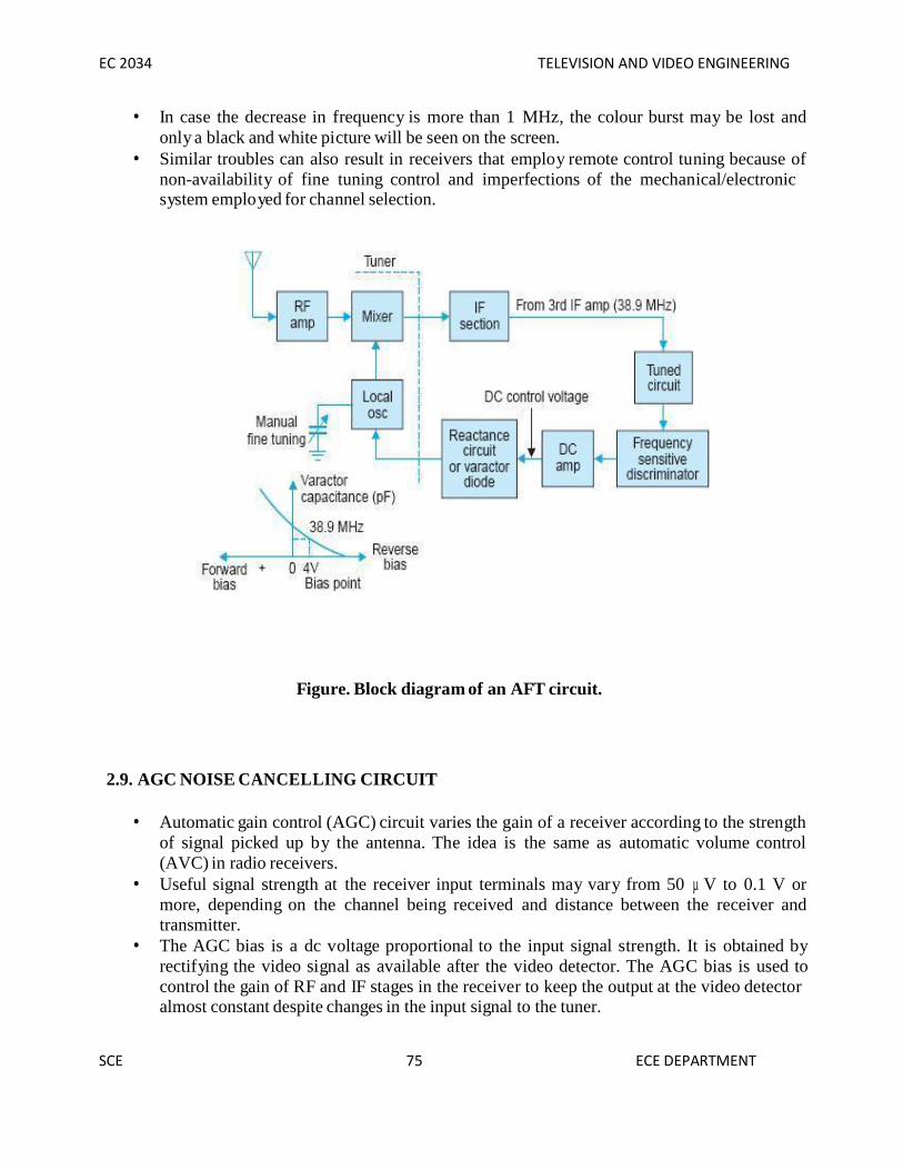
EC 2034 TELEVISION AND VIDEO ENGINEERING
SCE 7575
ECE DEPARTMENT
In case the decrease in frequency is more than 1 MHz, the colour burst may be lost andonly a black and white picture will be seen on the screen.
Similar troubles can also result in receivers that employ remote control tuning because ofnon-availability of fine tuning control and imperfections of the mechanical/electronicsystem employed for channel selection.
Figure. Block diagram of an AFT circuit.
2.9. AGC NOISE CANCELLING CIRCUIT
Automatic gain control (AGC) circuit varies the gain of a receiver according to the strengthof signal picked up by the antenna. The idea is the same as automatic volume control(AVC) in radio receivers.
Useful signal strength at the receiver input terminals may vary from 50 µ V to 0.1 V ormore, depending on the channel being received and distance between the receiver andtransmitter.
The AGC bias is a dc voltage proportional to the input signal strength. It is obtained byrectifying the video signal as available after the video detector. The AGC bias is used tocontrol the gain of RF and IF stages in the receiver to keep the output at the video detectoralmost constant despite changes in the input signal to the tuner.

EC 2034 TELEVISION AND VIDEO ENGINEERING
SCE 7676
ECE DEPARTMENT
ADVANTAGES OF AGC
The advantages of AGC are:
(a) Intensity and contrast of the picture, once set with manual controls, remain almostconstant despite changes in the input signal strength, since the AGC circuit reduces gain of thereceiver with increase in input signal strength.
(b) Contrast in the reproduced picture does not change much when the receiver is switchedfrom one station to another.
(c) Amplitude and cross modulation distortion on strong signals is avoided due to reductionin gain.
(d) AGC also permits increase in gain for weak signals. This is achieved by delaying theapplication of AGC to the RF amplifier until the signal strength exceeds 150 µ V or so. Thereforethe signal to noise ratio remains large even for distant stations. This reduces snow effect in thereproduced picture.
(e) Flutter in the picture due to passing aero planes and other fading effects is reduced.(f) Sound signal, being a part of the composite video signal, is also controlled by AGC and
thus stays constant at the set level.(g) Separation of sync pulses becomes easy since a constant amplitude video signal
Becomes available for the sync separator. AGC does not change the gain in a strictly linear fashionwith change in signal strength, but overall control is quite good. For example, with an antennasignal of 200 µ V the combined RF and IF section gain will be 10,000 to deliver 2 V of video signalat the detector output, whereas with an input of 2000 µ V, the gain instead of falling to 1000 todeliver the same output, might attain a value of 1500 to deliver 3 V at the video detector.
Basic AGC Circuit
Figure. Basic AGC circuit.

EC 2034 TELEVISION AND VIDEO ENGINEERING
SCE 7777
ECE DEPARTMENT
The circuit of Fig. illustrates how AGC bias is developed and fed to RF and IF amplifiers.The video signal on rectification develops a unidirectional voltage across RL. This voltagemust be filtered since a steady dc voltage is needed for bias. R1 and C1, with a time constantof about 0.2 seconds, constitute the AGC filter.
A smaller time constant, will fail to remove low frequency variations in the rectified signal,whereas, too large a time constant will not allow the AGC bias to change fast enough whenthe receiver is tuned to stations having different signal strengths.
In addition, a large time constant will fail to suppress flutter in the picture which occurs onaccount of unequal signal picked up by the antenna after reflection from the wings of anaero plane flying nearby.
With tubes, a typical AGC filter has 0.1 µ F for C1 and 2 M for R1. For transistors, typicalvalues are 20 k for R1 and 10 µ F for C1. The filtered output voltage across C1 is the sourceof AGC bias to be distributed by the AGC line.
Each stage controlled by AGC has a return path to the AGC line for bias, and thus thevoltage on the AGC line varies the bias of the controlled stages.
2.12. DC REINSERTION
As explained earlier, relative relationship of ac signal to the blanking and sync pulsesremains same with or without the dc component. Furthermore, brighter the line, greater isthe separation between the picture information variations and the associated pulses.
As the scene becomes darker, the two components move closer to each other. It is fromthese relationships that a variable bias can be developed to return the pulses to the samelevel which existed before the signal was applied to the RC network.
DC Restoration with a Diode. A simple transistor-diode clamp circuit for lining up syncpulses is shown in Fig. The V CC supply is set for a quiescent voltage of 15 V. In theabsence of any input signal the coupling capacitor ‘C’ charges to 15 V and so the voltageacross the parallel combination of resistor R and diode D will be zero. Assume that onapplication of a video signal, the collector voltage swings by 8 V peak to peak.
The corresponding variations in collector to emitter voltage are illustrated in Fig. Thepositive increase in collector voltage is coupled through C to the anode of diode D, turningit on. Since a forward biased diode may be considered to be a short, it effectively ties(clamps) the output circuit to ground (zero level). In effect, each positive sync pulse tipwill be clamped to zero level, thereby lining them up and restoring the dc level of the videosignal.
In the case under consideration the diode will cause the coupling capacitor to charge to apeak value of 19 V. However, during negative excursion of the collector voltage thecapacitor fails to discharge appreciably, because the diode is now reverse biased and thevalue of R has been chosen to be quite large.
The average reverse bias across the diode is – 4 V, being the difference between thequiescent collector voltage and peak value across the capacitor. Note that as the input video

EC 2034 TELEVISION AND VIDEO ENGINEERING
SCE 7878
ECE DEPARTMENT
signal varies in amplitude a corresponding video signal voltage appears across the resistorR and it varies in amplitude from 0 to – 8 V (peak to peak). This, as shown in Fig., is thecomposite video signal clamped to zero.
Similarly as and when the average brightness of the scene varies the capacitor C chargesto another peak value thereby keeping the sync tips clamped to zero level. Reversing thediode in the restorer circuit will result in negative peak of the input signal being clampedto zero.
This would mean that the dc output voltage of the circuit will be positive. The video signalcan also be clamped to any other off-set voltage by placing a dc voltage of suitable polarityin series with the clamping diode.
Limitations of Diode Clamping
It was assumed while explaining the mechanism of dc restoration that charge across thecoupling Capacitor C does not change during negative swings of the collector voltage.However, it is not so because of the finite value of RC.
The voltage across C does change somewhat when the condenser tends to dischargethrough the resistor R. Another aspect that merits attention is the fact that whenever averagebrightness of the picture changes suddenly the dc restorer is not capable of instant responsebecause of inherent delay in the charge and discharge of the capacitor.
Some receivers employ special dc restoration techniques but cost prohibits their use inaverage priced sets.
Figure. Diode dc restorer (a) circuit (b) collector voltage (c) output voltage applied to thegrid of the tube.

EC 2034 TELEVISION AND VIDEO ENGINEERING
SCE 7979
ECE DEPARTMENT
This, being positive, reduces the net negative voltage between the grid and cathode and thescene then moves to a brighter area on the picture tube characteristics.
Any decrease in average brightness of the scene being televised will have the oppositeeffect and net grid bias will become more negative to reduce background illumination ofthe picture on the raster.
Thus the diode with the associated components serves to restore the dc content of thepicture signal and the difference in potential between ‘X’ and ‘Y’ serves as a variable dcbias to change the average brightness of the scene.
2.13. VIDEO AMPLIFIER CIRCUIT
A transistorized video amplifier circuit with emitter follower drive and partial dc couplingis shown in Fig. The salient features of this circuit are :
(i) Signal from the video detector is dc coupled to the base of Q 1 . This transistor combinesthe functions of an emitter follower and CE amplifier. The high input impedance of emitterfollower minimizes loading of the video detector. The sync circuit is fed from the collector of thistransistor, where as signal for the sound section and AGC circuit is taken from the output of theemitter follower.
(ii) The output from the emitter follower is dc coupled to the base of Q 2 . This is a 5 W powertransistor, with a heat-sink mounted on the case. The collector supply is 140 V, to provide enoughvoltage swing for the 80 V P-P video signal output.
(iii) In the output circuit of Q 2 , contrast control forms part of the collector load. The videooutput signal is coupled by the 0.22 μF (C 2 ) capacitor to the cathode of picture tube. The partialdc coupling is provided by the 1 M (R 2 ) resistor connected at the collector of Q 2 .
(iv) The parallel combination of L 1 and C 1 is tuned to resonate at 5.5 MHz to providemaximum negative feedback to the sound signal. This prevents appearance of sound signal at theoutput of video amplifier.
(v) The neon bulb in the grid circuit provides protection of a spark-gap since the neon bulbionizes and shorts to ground with excessive voltage. The ‘spark gaps’ are employed to protectexternal receiver circuitry from ‘flash overs’ within the tube. The accumulation of charge at thevarious electrodes of the picture tube results in the appearance of high voltages at the electrodes,which if not discharged to ground, will do so through sections of the receiver circuitry and causedamage.
(vi) Note that dc voltages at the base and emitter of the two transistors have been suitably setto give desired forward bias.
(vii) Vertical retrace blanking pulses are fed at the grid of the picture tube through C 3, and thegrid-return to ground is provided by R 3 .
(viii) Brightness control. The adjustment of average brightness of the reproduced scene iscarried out by varying the bias potential between cathode and control grid of the picture tube. Inthe circuit being considered a 100 KΩ potentiometer is provided to adjust dc voltage at the cathode.
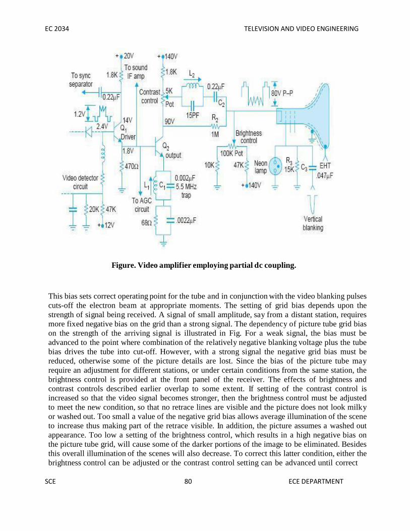
EC 2034 TELEVISION AND VIDEO ENGINEERING
SCE 8080
ECE DEPARTMENT
Figure. Video amplifier employing partial dc coupling.
This bias sets correct operating point for the tube and in conjunction with the video blanking pulsescuts-off the electron beam at appropriate moments. The setting of grid bias depends upon thestrength of signal being received. A signal of small amplitude, say from a distant station, requiresmore fixed negative bias on the grid than a strong signal. The dependency of picture tube grid biason the strength of the arriving signal is illustrated in Fig. For a weak signal, the bias must beadvanced to the point where combination of the relatively negative blanking voltage plus the tubebias drives the tube into cut-off. However, with a strong signal the negative grid bias must bereduced, otherwise some of the picture details are lost. Since the bias of the picture tube mayrequire an adjustment for different stations, or under certain conditions from the same station, thebrightness control is provided at the front panel of the receiver. The effects of brightness andcontrast controls described earlier overlap to some extent. If setting of the contrast control isincreased so that the video signal becomes stronger, then the brightness control must be adjustedto meet the new condition, so that no retrace lines are visible and the picture does not look milkyor washed out. Too small a value of the negative grid bias allows average illumination of the sceneto increase thus making part of the retrace visible. In addition, the picture assumes a washed outappearance. Too low a setting of the brightness control, which results in a high negative bias onthe picture tube grid, will cause some of the darker portions of the image to be eliminated. Besidesthis overall illumination of the scenes will also decrease. To correct this latter condition, either thebrightness control can be adjusted or the contrast control setting can be advanced until correct
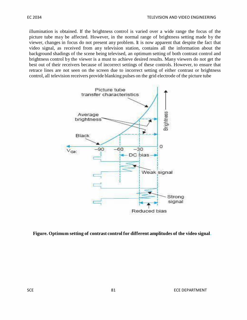
EC 2034 TELEVISION AND VIDEO ENGINEERING
SCE 8181
ECE DEPARTMENT
illumination is obtained. If the brightness control is varied over a wide range the focus of thepicture tube may be affected. However, in the normal range of brightness setting made by theviewer, changes in focus do not present any problem. It is now apparent that despite the fact thatvideo signal, as received from any television station, contains all the information about thebackground shadings of the scene being televised, an optimum setting of both contrast control andbrightness control by the viewer is a must to achieve desired results. Many viewers do not get thebest out of their receivers because of incorrect settings of these controls. However, to ensure thatretrace lines are not seen on the screen due to incorrect setting of either contrast or brightnesscontrol, all television receivers provide blanking pulses on the grid electrode of the picture tube
Figure. Optimum setting of contrast control for different amplitudes of the video signal.
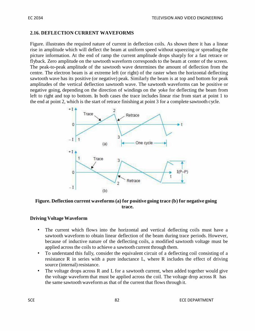
EC 2034 TELEVISION AND VIDEO ENGINEERING
SCE 8282
ECE DEPARTMENT
2.16. DEFLECTION CURRENT WAVEFORMS
Figure. illustrates the required nature of current in deflection coils. As shown there it has a linearrise in amplitude which will deflect the beam at uniform speed without squeezing or spreading thepicture information. At the end of ramp the current amplitude drops sharply for a fast retrace orflyback. Zero amplitude on the sawtooth waveform corresponds to the beam at center of the screen.The peak-to-peak amplitude of the sawtooth wave determines the amount of deflection from thecentre. The electron beam is at extreme left (or right) of the raster when the horizontal deflectingsawtooth wave has its positive (or negative) peak. Similarly the beam is at top and bottom for peakamplitudes of the vertical deflection sawtooth wave. The sawtooth waveforms can be positive ornegative going, depending on the direction of windings on the yoke for deflecting the beam fromleft to right and top to bottom. In both cases the trace includes linear rise from start at point 1 tothe end at point 2, which is the start of retrace finishing at point 3 for a complete sawtooth cycle.
Figure. Deflection current waveforms (a) for positive going trace (b) for negative goingtrace.
Driving Voltage Waveform
The current which flows into the horizontal and vertical deflecting coils must have asawtooth waveform to obtain linear deflection of the beam during trace periods. However,because of inductive nature of the deflecting coils, a modified sawtooth voltage must beapplied across the coils to achieve a sawtooth current through them.
To understand this fully, consider the equivalent circuit of a deflecting coil consisting of aresistance R in series with a pure inductance L, where R includes the effect of drivingsource (internal) resistance.
The voltage drops across R and L for a sawtooth current, when added together would givethe voltage waveform that must be applied across the coil. The voltage drop across R hasthe same sawtooth waveform as that of the current that flows through it.

EC 2034 TELEVISION AND VIDEO ENGINEERING
Figure. Current and voltage wave shapes in a deflection coil(a) voltage drop across the resistive component of coil impedance
(b) voltage drop across the inductive component of coil impedance(c) resultant voltage ‘v’ (VR + vL) across input terminals of the
coil for a sawtooth current in the winding.
A faster change in i L , produces more self induced voltage v L . Furthermore, for a constantrate of change in i L , the value of v L is constant. As a result, v L in Fig. is at a relativelylow level during trace time, but because of fast drop in i L during the retrace period, a sharpvoltage peak or spike appears across the coil.
The polarity of the flyback pulse is opposite to the trace voltage, because i L is thendecreasing instead of increasing. Therefore, a sawtooth current in L produces a rectangularvoltage.
This means, that to produce a sawtooth current in an inductor, a rectangular voltage shouldbe applied across it. When the voltage drops across R and L are added together, the resultis a trapezoidal waveform.
Thus to produce a sawtooth current in a circuit having R and L in series, which in the case.
SCE 83 ECE DEPARTMENT

EC 2034 TELEVISION AND VIDEO ENGINEERING
SCE 8484
ECE DEPARTMENT
Figure. Inverted polarity of i and v.
2.16. DEFLECTION OSCILLATORS
Under consideration represents a deflection coil, a trapezoidal voltage must be appliedacross it. Note that for a negative going sawtooth current, the resulting trapezoid willnaturally have an inverted polarity as illustrated in Fig.
As explained above, for linear deflection, a trapezoidal voltage wave is necessary acrossthe vertical deflecting coils. However, the resulting voltage waveform for the horizontalyoke will look closer to a rectangular wave shape, because voltage across the inductoroverrides significantly the voltage across the resistance on account of higher rate of riseand fall of coil current. Effect of Driving Source Impedance on Wave shapes.
In deflection circuits employing vacuum tubes, the magnitude of R is quite large becauseof high plate resistance of the tube. Therefore, voltage wave shape across the verticaldeflection coils and that needed to drive the vertical output stage is essentially trapezoidal.However, in a horizontal output circuit employing a tube, the wave shape will be close torectangular because of very high scanning frequency.
When transistors are employed in vertical and horizontal deflection circuits, the drivingimpedance is very low and equivalent yoke circuits appear to be mainly inductive. Thisneeds an almost rectangular voltage wave shape across the yoke.
To produce such a voltage wave shape, the driving voltage necessary for horizontal andvertical scanning circuits would then be nearly rectangular. Thus the driving voltagewaveforms to be generated by the deflection oscillator circuits would vary depending ondeflection frequency, device employed and deflection coil impedance.

EC 2034 TELEVISION AND VIDEO ENGINEERING
SCE 8585
ECE DEPARTMENT
Deflection Oscillators
In order to produce a picture on the screen of a TV receiver that is in synchronism with theone scanned at the transmitting end, it is necessary to first produce a synchronized raster.The video signal that is fed to the picture tube then automatically generates a copy of thetransmitted picture on the raster.
While actual movement of the electron beam in a picture tube is controlled by magneticfields produced by the vertical and horizontal deflection coils, proper vertical andhorizontal driving voltages must first be produced by synchronized oscillators andassociated wave shaping circuits. As illustrated in Fig.
For vertical deflection the frequency is 50 Hz, while for horizontal deflection it is 15625Hz. The driving waveforms thus generated are applied to power amplifiers which providesufficient current to the deflecting coils to produce a full raster on the screen of picturetube.
Free running relaxation type of oscillators are preferred as deflection voltage sourcesbecause these are most suited for generating the desired output waveform and can be easilylocked into synchronism with the incoming sync pulses.
The oscillators commonly used in both vertical and horizontal deflection sections of thereceiver are:
(i) Blocking oscillator,(ii) Multivibrator,(iii) Complementary pair relaxation oscillator,(iv) Overdriven sine-wave oscillator.
It may be noted that complementary pair circuits are possible only with transistors whileall other types may employ tubes or transistors.
As explained earlier, both vertical and horizontal deflection oscillators must lock withcorresponding incoming sync pulses directly or indirectly to produce a stable televisionpicture.

EC 2034 TELEVISION AND VIDEO ENGINEERING
SCE 8686
ECE DEPARTMENT
2.20. TELEVISION RECEIVER ANTENNAS
For both VHF and UHF television channels, one-half-wave length is a practical size andtherefore an ungrounded resonant dipole is the basic antenna often employed for receptionof television signals.
The dipole intercepts radiated electromagnetic waves to provide induced signal current inthe antenna conductors.
A matched transmission line connects the antenna to the input terminals of the receiver. Itmay be noted that the signal picked up by the antenna contains both picture and soundsignal components.
This is possible, despite the 5.5 MHz separation between the two carriers, because of thelarge bandwidth of the antenna. In fact a single antenna can be designed to receive signalsfrom several channels that be close to each other.
Antennas for VHF Channels Although most receivers can produce a picture with sufficient contrast even with a weak
signal, but for a picture with no snow and ghosts, the required antenna signal strength liesbetween 100 and 2000 μV.
Thus, while a half-wave dipole will deliver satisfactory signal for receivers located closeto the transmitter, elaborate arrays become necessary for locations far away from thetransmitter.
Yagi-Uda Antenna
The antenna widely used with television receivers for locations within 40 to 60 km fromthe transmitter is the folded dipole with one reflector and one director. This is commonlyknown as Yagi-Uda or simply Yagi antenna.
The elements of its array as shown in Fig. are arranged collinearly and close together. Thisantenna provides a gain close to 7 db and is relatively unidirectional as seen from itsradiation pattern drawn in Fig.
These characteristics are most suited for reception from television transmitters of moderatecapacity. To avoid pick-up from any other side, the back lobe of the radiation pattern canbe reduced by bringing the radiators closer to each other.
The resultant improvement in the front to back ratio of the signal pick-up makes the antennahighly directional and thus can be oriented for efficient pick-up from a particular station.
However, bringing the radiators closer has the adverse effect of lowering the inputimpedance of the array.

EC 2034 TELEVISION AND VIDEO ENGINEERING
SCE 8787
ECE DEPARTMENT
Figure. Yagi-Uda antenna (a) antenna (b) radiation pattern.
As mentioned earlier, it is not necessary to erect a separate antenna for each channelbecause the resonant circuit formed by the antenna is of low ‘Q’ (quality factor) and assuch has a broad band response.
For the lower VHF channels (Band I—channels 2 to 4) the length of the antenna may becomputed for a middle value. While this antenna will not give optimum results at otherfrequencies, the reception will still be quite satisfactory in most cases if the stations are notlocated far away. Though the antenna length used should be as computed by the usualexpression:
Wavelength (λ) = 3 × 10 8 meters, But in practice it is kept about 6 percent less than the f (Hz) calculated value. This is
necessary because the self-capacitance of the antenna alters the current distribution at itsends. The small distance between the two quarter wave rods of the driver, where the lead-in line is connected can be taken as too small and hence neglected. Note that this gap doesnot affect the current distribution significantly.
Antenna Mounting
The receiving antenna is mounted horizontally for maximum pick-up from the transmittingantenna. As stated earlier, horizontal polarization results in more signal strength, lessreflection and reduced ghost images.
The antenna elements are normally made out of 1/4′′ (0.625 cm) to 1/2′′ (1.25 cm) diaaluminum pipes of suitable strength.

EC 2034 TELEVISION AND VIDEO ENGINEERING
SCE 8888
ECE DEPARTMENT
The thickness of the pipe should be so chosen that the antenna structure does not get bentor twisted during strong winds or occasional sitting and flying off of birds. A hollowconductor is preferred because on account of skin effect, most of the current flows over theouter surface of the conductor.
The antenna is mounted on a suitable structure at a height around 10 metres above theground level. This not only insulates it from the ground but results in induction of largesignal strength which is free from any interference. The centre of the closed section of thehalf-wave folded dipole is a point of minimum voltage, allowing direct mounting at thispoint to the grounded metal mast without shorting the signal voltage.
A necessary precaution while mounting the antenna is that it should be at least two metresaway from other antennas and large metal objects. In crowded city areas close to thetransmitter, the resultant signal strength from the antenna can sometimes be very low onaccount of out of phase reflections from surrounding buildings.
In such situations, changing the antenna placement only about a metre horizontally orvertically can make a big difference in the strength of the received signal, because ofstanding waves set up in such areas that have large conductors nearby. Similarly rotatingthe antenna can help minimize reception of reflected signals, thereby eliminating theappearance of ghost images.
In areas where several stations are located nearby, antenna rotators are used to turn itsdirection. These are operated by a motor drive to set the broad side of the antenna foroptimum reception from the desired station.
However, in installations where a rotating mechanism is not provided, it is a good practiceto connect the antenna to the receiver before it is fixed in place permanently and proceedas detailed below:
(i) Try changing the height of the antenna to obtain maximum signal strength.(ii) Rotate the antenna to check against ghost images and reception of signals from
far-off stations.(iii) When more than one station is to be received, the final placement must be a
compromise for optimum reception from all the stations in the area. In extreme cases, itmay be desirable to erect more than one antenna.
Indoor Antennas In strong signal areas it is sometimes feasible to use indoor antennasprovided the receiver is sufficiently sensitive. These antennas come in a variety of shapes.
Most types have selector switches which are used for modifying the response pattern bychanging the resonant frequency of the antenna so as to minimize interference and ghostsignals.
Generally the switch is rotated with the receiver on, until the most satisfactory picture isobtained on the screen. Almost all types of indoor antennas have telescopic dipole rodsboth for adjusting the length and also for folding down when not in use.
Fringe Area Antenna In fringe areas where the signal level is very low, high-gain antenna arrays are needed. The
gain of the antenna increases with the number of elements employed. A Yagi antenna witha large number of directors is commonly used with success in fringe areas for stations inthe VHF band.

EC 2034 TELEVISION AND VIDEO ENGINEERING
SCE 8989
ECE DEPARTMENT
As already mentioned, a parasitic element resonant at a lower frequency than the drivenelement will act as a mild reflector, and a shorter parasitic element will act as a mild‘concentrator’ of radiation.
As a parasitic element is brought closer to the driven element, then regardless of its preciselength, it will load the driven element more and therefore reduce its input impedance.
This is perhaps the main reason for invariable use of a folded dipole as the driven elementof such an array. A gain of more than 10 db with a forward to back ratio of about 15 iseasily obtained with such an antenna. Such high gain combinations are sharply directionaland so must be carefully aimed while mounting, otherwise the captured signal will be muchlower than it should be.
A typical Yagi antenna for use in fringe areas is shown in Fig.
Fig. A typical Yagi antenna, (b) Channel four antenna.
In such antennas the reflectors are usually 5 per cent longer than the dipole and may bespaced from it at 0.15 to 0.25 wavelength depending on design requirements.
Similarly the directors may be 4 per cent shorter than the antenna element, but wherebroadband characteristics are needed successive directors are usually made shorter (seeFig.) to be resonant for the higher frequency signals of the spectrum.
In some fringe area installations, transistorized booster amplifiers are also used along withthe Yagi antenna to improve reception.
These are either connected just close to the antenna or after the transmission line, beforethe signal is delivered to the receiver.

EC 2034 TELEVISION AND VIDEO ENGINEERING
SCE 9090
ECE DEPARTMENT
Yagi Antenna Design
The following expressions can be used as a starting point while designing any Yagi antennaarray.Length of dipole (in metres) ≈143( f is the centre frequency of the channel) f (MHz)Length of reflector (in metres) ≈ 152/f (MHz)Length of first director (in metres) ≈ 137/f (MHz)
Length of subsequent directors reduces progressively by 2.5 per cent. Spacing between reflector and dipole = 0.25λ ≈ 75/f (MHz) Spacing between director and dipole = 0.13λ ≈ 40/f (MHz) Spacing between director and director = 0.13λ ~ − 39/f (MHz)
The above lengths and spacings are based on elements of 1 to 1.2 cm in diameter. It maybe noted that length of the folded dipole is measured from centre of the fold at one end tothe centre of the fold at the other end.
It must be remembered that the performance of Yagi arrays can only be assessed if all thecharacteristics like impedance, gain, directivity and bandwidth are taken into accounttogether. Since there are so many related variables, the dimensions of commercial antennasmay differ from those computed with the expressions given above.
However, for single channel antennas the variation is not likely to be much. Figure showsa dimensioned sketch of channel four (61 to 68 MHz) antenna designed for locations nottoo far from the transmitter. It has an impedance = 40 + j20 Ω, a front to back pick up ratio= 30 db, and an overall length = 0.37 wavelength.
Multiband Antennas
It is not possible to receive all the channels of lower and higher VHF band with oneantenna. The main problem in using one dipole for both the VHF bands is the difficulty ofmaintaining a broadside response.
This is because the directional pattern of a low-band dipole splits into side lobes at the thirdand fourth harmonic frequencies in the 174 to 223 MHz band. On the other hand a high-band dipole cut for a half wavelength in the 174 to 233 MHz band is not suitable for the 47to 68 MHz band because of insufficient signal pick-up at the lower frequencies.
As a result, antennas for both the VHF bands generally use either separate dipoles for eachband or a dipole for the lower VHF band modified to provide broadside unidirectionalresponse in the upper VHF band also.

EC 2034 TELEVISION AND VIDEO ENGINEERING
SCE 9191
ECE DEPARTMENT
Diplexing of VNF Antennas
When it is required to combine the outputs from the lower and upper VHF band antennasto a common lead-in wire (feeder) it is desirable to employ a filter network that not onlymatches the signal sources to the common feeder but also isolates the signals in theantennas from each other.
Such a filter arrangement is called a ‘diplexer’. Its circuit with approximate componentvalues for bands I (47 to 68 MHz) and III (174 to 263 MHz) is given in Fig.
Figure. Diplexing antenna outputs (a) diplexer network,
H.P.-L.P.-filter combination (b) diplexer connections.
The manner in which it is connected to the two antennas is shown in Fig. Similarly atriplexer filter can be employed when three different antennas are to feed their outputs to acommon socket in the receiver.
The combining arrangement can be further modified to connect the output from a UHFantenna to the same feeder line.
EC 2034 TELEVISION AND VIDEO ENGINEERING
SCE 9292
ECE DEPARTMENT
UNIT IIIESSENTIALS OF COLOR TELEVISION
3.1. COMPATIBILITY
Regular color TV broadcast could not be started till 1954 because of the stringentrequirement of making color TV compatible with the existing monochrome system.Compatibility implies that
(i) The color television signal must produce a normal black and white picture on amonochrome receiver without any modification of the receiver circuitry
(ii) A color receiver must be able to produce a black and white picture from a normalmonochrome signal. This is referred to as reverse compatibility.
To achieve this, that is to make the system fully compatible the composite color signal must meetthe following requirements:(i) It should occupy the same bandwidth as the corresponding monochrome signal.(ii) The location and spacing of picture and sound carrier frequencies should remain the same.(iii) The color signal should have the same luminance (brightness) information as would amonochrome signal, transmitting the same scene.(iv) The composite color signal should contain color information together with the ancillarysignals needed to allow this to be decoded.(v) The color information should be carried in such a way that it does not affect the picturereproduced on the screen of a monochrome receiver.(vi) The system must employ the same deflection frequencies and sync signals as used formonochrome transmission and reception.
In order to meet the above requirements it becomes necessary to encode the colorinformation of the scene in such a way that it can be transmitted within the same channelbandwidth of 7 MHz and without disturbing the brightness signal. Similarly at thereceiving end a decoder must be used to recover the color signal back in its original formfor feeding it to the tri-color picture tube. Before going into details of encoding anddecoding the picture signal, it is essential to gain a good understanding of thefundamental properties of light. It is also necessary to understand mixing of colors toproduce different hues on the picture screen together with limitations of the human eye toperceive them. Furthermore a knowledge of the techniques employed to determinedifferent colors in a scene and to generate corresponding signal voltages by the colortelevision camera is equally essential.
3.2. COLOR PERCEPTION
All objects that we observe are focused sharply by the lens system of the eye on its retina.The retina which is located at the back side of the eye has light sensitive organs whichmeasure the visual sensations.
The retina is connected with the optic nerve which conducts the light stimulias sensed bythe organs to the optical centre of the brain. According to the theory formulated byHelmholtz the light sensitive organs are of two types rods and cones.

EC 2034 TELEVISION AND VIDEO ENGINEERING
SCE 9393
ECE DEPARTMENT
The rods provide brightness sensation and thus perceive objects only in various shades ofgrey from black to white. The cones that are sensitive to color are broadly in threedifferent groups. One set of cones detects the presence of blue color in the object focusedon the retina, the second set perceives red color and the third is sensitive to the greenrange. Each set of cones, may be thought of as being ‘tuned’ to only a small band offrequencies and so absorb energy from a definite range of electromagnetic radiation toconvey the sensation of corresponding color or range of color.
The combined relative luminosity curve showing relative sensation of brightnessproduced by individual spectral colors radiated at a constant energy level is shown in Fig.It will be seen from the plot that the sensitivity of the human eye is greatest for greenlight, decreasing towards both the red and blue ends of the spectrum.
In fact the maximum is located at about 550 nm, a yellow green, where the spectralenergy maximum of sunlight is also located.
Figure. Approximate relative response of the eye to different colors
3.3. THREE COLOR THEORY All light sensations to the eye are divided (provided there is an adequate brightness
stimulus on the operative cones) into three main groups. The optic nerve system thenintegrates the different color impressions in accordance with the curve shown in Fig.toperceive the actual color of the object being seen.
This is known as additive mixing and forms the basis of any color television system. Ayellow color, for example, can be distinctly seen by the eye when the red and greengroups of the cones are excited at the same time with corresponding intensity ratio.
EC 2034 TELEVISION AND VIDEO ENGINEERING
Similarly and color other than red, green and blue will excite different sets of cones togenerate the cumulative sensation of that color.
A white color is then perceived by the additive mixing of the sensations from all the threesets of cones. Mixing of Colors Mixing of colors can take place in two ways subtractivemixing and additive mixing.
In subtractive mixing, reflecting properties of pigments are used, which absorb allwavelengths but for their characteristic color wavelengths.
When pigments of two or more colors are mixed, they reflect wavelengths which arecommon to both. Since the pigments are not quite saturated (pure in color) they reflect afairly wide band of wavelengths.
This type of mixing takes place in painting and color printing. In additive mixing whichforms the basis of color television, light from two or more colors obtained either fromindependent sources or through filters can create a combined sensation of a differentcolor.
Thus different colors are created by mixing pure colors and not by subtracting parts fromwhite. The additive mixing of three primary colors red, green and blue in adjustableintensities can create most of the colors encountered in everyday life.
The impression of white light can also be created by choosing suitable intensities of thesecolors. Red, green and blue are called primary colors. These are used as basic colors intelevision. By pairwise additive mixing of the primary colors the followingcomplementary colors are produced:
Red + Green = YellowRed + Blue = Magenta (purplish red shade)Blue + Green = Cyan (greenish blue shade)
Color plate 1 depicts the location of primary and complementary colors on the colorcircle. If a complementary is added in appropriate proportion to the primary which ititself does not contain, white is produced.
This is illustrated in Fig. where each circle corresponds to one primary color. Color plate2 shows the effect of color mixing. Similarly Fig, illustrates the process of subtractivemixing. Note that as additive mixing of the three primary colors produces white, theirsubtractive mixing results in black.
(Research has shown that the actual neural process of color perception is substantiallydifferent from the tricolor process. However, all color reproduction processes intelevision or printing use variations of this process and is found satisfactory).
SCE 94 ECE DEPARTMENT

EC 2034 TELEVISION AND VIDEO ENGINEERING
Figure. Additive color mixing. The diagram shows the effect of projecting green, red andblue beams on a white screen in such a way that they overlap
Figure. Subtractive color mixing. The diagram shows the effect of mixing color pigmentsunder white light.
SCE 95 ECE DEPARTMENT
EC 2034 TELEVISION AND VIDEO ENGINEERING
SCE 9696
ECE DEPARTMENT
3.4. LUMINANCE, HUE AND SATURATION
Any color has three characteristics to specify its visual information. These are (i)luminance,(ii) hue or tint, and (iii) saturation. These are defined as follows:
(i) Luminance or Brightness
This is the amount of light intensity as perceived by the eye regardless of the color. Inblack and white pictures, better lighted parts have more luminance than the dark areas.Different colors also have shades of luminance in the sense that though equallyilluminated appear more or less bright as indicated by the relative brightness responsecurve of Fig. Thus on a monochrome TV screen, dark red color will appear as black,yellow as white and a light blue color as grey.
(ii) Hue This is the predominant spectral color of the received light. Thus the color of any object
is distinguished by its hue or tint. The green leaves have green hue and red tomatoes havered hue. Different hues result from different wavelengths of spectral radiation and areperceived as such by the sets of cones in the retina.
(iii)Saturation This is the spectral purity of the color light. Since single hue colors occur rarely alone,
this indicates the amounts of other colors present. Thus saturation may be taken as anindication of how little the color is diluted by white. A fully saturated color has no white.As an example. Vivid green is fully saturated and when diluted by white it becomes lightgreen. The hue and saturation of a color put together is known as chrominance. Note thatit does not contain the brightness information. Chrominance is also called chroma.
Chromaticity Diagram.
Chromaticity diagram is a convenient space coordinate representation of all the spectralcolors and their mixtures based on the tristimulus values of the primary colors containedby them. Fig. is a two dimensional representation of hue and saturation in the X-Y plane(see color plate 3).
If a three dimensional representation is drawn, the ‘Z’ axis will show relative brightnessof the color. As seen in the figure the chromaticity diagram is formed by all the rainbowcolors arranged along a horseshoe-shaped triangular curve.
The various saturated pure spectral colors are represented along the perimeter of thecurve, the corners representing the three primary colors red, green and blue. As thecentral area of the triangular curve is approached, the colors become de-saturatedrepresenting mixing of colors or a white light.
The white lies on the central point ‘C’ with coordinates x = 0.31 and y = 0.32. Actuallythere is no specific white light sunlight, skylight, daylight are all forms of white light.

EC 2034 TELEVISION AND VIDEO ENGINEERING
SCE 9797
ECE DEPARTMENT
The illuminant ‘C’ marked in Fig. (a) Represents a particular white light formed bycombining hues having wavelength: 700 nm (red) 546.1 nm (green) and 438.8 nm (blue)with proper intensities.
This shade of white which has been chosen to represent white in TV transmission andreception also corresponds to the subjective impression formed in the human eye byseeing a mixture of 30 percent of red color, 59 percent of green color and 11 percent ofthe blue color at wavelengths specified above.
A practical advantage of the chromaticity diagram is that, it is possible to determine theresult of additive mixing of any two or more color lights by simple geometricconstruction.
The color diagram contains all colors of equal brightness. Since brightness is representedby the ‘Z’ axis, as brightness increase, the color diagram becomes larger as shown in Fig.
Figure. Chromaticity diagram. Note that red, green and blue have been standardized atwavelengths of 700, 646.1 and 438.8 nanometers respectively. X and Y denote colorcoordinates. For example white lies at X = 0.31 and Y = 0.32.

EC 2034 TELEVISION AND VIDEO ENGINEERING
SCE 9898
ECE DEPARTMENT
Figure. Representation of luminance (brightness).
3.5. COLOR TELEVISION CAMERA
Figure. Plan of a color television camera showing generation of color signals and Y matrixfor obtaining the luminance (brightness) signal
EC 2034 TELEVISION AND VIDEO ENGINEERING
SCE 9999
ECE DEPARTMENT
Figure shows a simple block schematic of a color TV camera. It essentially consists ofthree camera tubes in which each tube receives selectively filtered primary colors.
Each camera tube develops a signal voltage proportional to the respective color intensityreceived by it. Light from the scene is processed by the objective lens system. The imageformed by the lens is split into three images by means of glass prisms.
These prisms are designed as diachroic mirrors. A diachroic mirror passes onewavelength and rejects other wavelengths (colors of light).Thus red, green, and blue colorimages are formed. The rays from each of the light splitters also pass through color filterscalled trimming filters.
These filters provide highly precise primary color images which are converted into videosignals by image-orthicon or vidicon camera tubes. Thus the three color signals aregenerated. These are called Red (R), Green (G) and Blue (B) signals. Simultaneousscanning of the three camera tubes is accomplished by a master deflection oscillator andsync generator which drives all the three tubes.
The three video signals produced by the camera represent three primaries of the colordiagram. By selective use of these signals, all colors in the visible spectrum can bereproduced on the screen of a special (color) picture tube.
Color Signal Generation
At any instant during the scanning process the transmitted signal must indicate theproportions, of red, green and blue lights which are present in the element being scanned.Besides this, to fulfil the requirements of compatibility, the luminance signal whichrepresents the brightness of the elements being scanned must also be generated andtransmitted along with the color signals.
Figure illustrates the method of generating these signals. The camera output voltages arelabelled as V R, V G and V B but generally the prefix V is omitted and only the symbolsR, G, and B are used to represent these voltages. With the specified source of white lightthe three cameras are adjusted to give equal output voltage.
Gamma Correction To compensate for the non-linearity of the system including TV camera and picture
tubes, a correction is applied to the voltages produced by the three camera tubes.
The output voltages are then referred as R′, G′ and B′. However, in our discussion we willignore such a distinction and use the same symbols i.e., R, G and B to represent gammacorrected output voltages.
Furthermore, for convenience of explanation the camera outputs corresponding tomaximum intensity (100%) of standard white light to be handled are assumed adjusted atan arbitrary value of one volt. Then on grey shades, i.e., on white of lesser brightness, R,G and B voltages will remain equal but at amplitude less than one volt.

EC 2034 TELEVISION AND VIDEO ENGINEERING
SCE 100100100
ECE DEPARTMENT
3.6. VALUES OF LUMINANCE (Y) AND COLOR DIFFERENCE SIGNALS
When televising color scenes even when voltages R, G and B are not equal, the ‘Y’ signalstill represents monochrome equivalent of the color because the proportions 0.3, 0.59 and0.11 taken of R, G and B respectively still represent the contribution which red, green andblue lights make to the luminance. This aspect can be illustrated by considering somespecific colors.
De-saturated Purple Consider a de-saturated purple color, which is a shade of magenta. Since the hue is
magenta (purple) it implies that it is a mixture of red and blue. Two word de-saturatedindicates that some white light is also there. The white light content will develop all thethree i.e., R, G and B voltages, the magnitudes of which will depend on the intensity ofdesaturation of the color.
Thus R and B voltages will dominate and both must be of greater amplitude than G. Asan illustration let R = 0.7, G = 0.2 and B = 0.6 volts. The white content is represented byequal quantities of the three primaries and the actual amount must be indicated by thesmallest voltage of the three, that is, by the magnitude of G.
Thus white is due to 0.2 R, 0.2 G and 0.2 B. The remaining, 0.5 R and 0.4 B togetherrepresent the magenta hue.
(i) The luminance signal Y = 0.3 R + 0.59 G + 0.11 B.Substituting the values of R, G, and B we get,Y = 0.3 (0.7) + 0.59 (0.2) + 0.11(0.6) = 0.394 (volts).
(ii) The color difference signals are:(R – Y) = 0.7 – 0.394 = + 0.306 (volts)(B – Y) = 0.6 – 0.394 = + 0.206 (volts)
(iii) Reception at the color receiver—At the receiver after demodulation, the signals,Y, (B – Y) and (R – Y), become available. Then by a process of matrixing the voltages B and Rare obtained as:
R = (R – Y) + Y = 0.306 + 0.394 = 0.7 VB = (B – Y) + Y = 0.206 + 0.394 = 0.6 V
(iv) (G – Y) matrix—The missing signal (G – Y) that is not transmitted can berecovered by using a suitable matrix based on the explanation given below:
Y = 0.3 R + 0.59G + 0.11Balso (0.3 + 0.59 + 0.11)Y = 0.3R + 0.59G + 0.11BRearranging the above expression we get:
0.59(G – Y) = – 0.3 (R – Y) – 0.11 (B – Y)∴ (G – Y) =− 03059.(R – Y) –0 11059.(B – Y) = – 0.51(R – Y) – 0.186 (B – Y)
Substituting the values of (R – Y) and (B – Y)(G – Y) = – (0.51 × 0.306) – 0.186(0.206) = – 0.15606 – 0.038216 = – 0.194∴ G = (G – Y) + Y = – 0.194 + 0.394 = 0.2,
and this checks with the given value.

EC 2034 TELEVISION AND VIDEO ENGINEERING
SCE 101101101
ECE DEPARTMENT
(v) Reception on a monochrome receiver Since the value of luminance signal Y = 0.394V,and the peak white corresponds to 1 volt (100%) the magenta will show up as a fairly dull greyin a black and white picture. This is as would be expected for this color.
De-saturated Orange A de-saturated orange having the same degree of desaturation as in the previous example
is considered now. Taking R = 0.7, G = 0.6, and B = 0.2, it is obvious that the outputvoltages due to white are R = 0.2, G = 0.2 and B = 0.2.
Then red and green colors which dominate and represent the actual color content with, R= 0.5 and G = 0.4 give the orange hue. Proceeding as in the previous example we get:
(i) Luminance signal Y = 0.3 R + 0.59G + 0.11 B. Substituting the values of R, G and B weget Y = 0.586 volt.(ii) Similarly, the color difference signal magnitudes are:
(R – Y) = (0.7 – 0.586) = + 0.114(B – Y) = (0.2 – 0.586) = – 0.386 and(G – Y) = – 0.51(R – Y) – 0.186(B – Y) = 0.014
(iii) At the receiver by matrixing we getR = (R – Y) + Y = 0.7G = (G – Y) + Y = 0.6B = (B – Y) + Y = 0.2
This checks with the voltages developed by the three camera tubes at the transmitting end.(iv) Reception on a monochrome receiver Only the luminance signal is received and, asexpected, with Y = 0.586, the orange hue will appear as bright grey.
3.7. COLOR TELEVISION DISPLAYTUBES
The color television picture tube screen is coated with three different phosphors, one foreach of the chosen red, green and blue primaries.
The three phosphors are physically separate from one another and each is energized by anelectron beam of intensity that is proportional to the respective color voltage reproducedin the television receiver.
The object is to produce three coincident raster’s with produce the red, green and bluecontents of the transmitted picture.
While seeing from a normal viewing distance the eye integrates the three colorinformation to convey the sensation of the hue at each part of the picture. Based on thegun configuration and the manner in which phosphors are arranged on the screen, threedifferent types of color picture tubes have been developed.
These are:1. Delta-gun color picture tube2. Guns-in-line or Precision-in-line (P-I-L) color picture tube.3. Single sun or Trinitron Color picture tube.

EC 2034 TELEVISION AND VIDEO ENGINEERING
SCE 102102102
ECE DEPARTMENT
3.8. DELTA-GUN COLOR PICTURE TUBE
This tube was first developed by the Radio Corporation of America (R.C.A.). It employsthree separate guns (see Fig. (a)), one for each phosphor. The guns are equally spaced at120° interval with respect to each other and tilted inwards in relation to the axis of thetube.
They form an equilateral triangular configuration. As shown in Fig. (b) The tube employsa screen where three color phosphor dots are arranged in groups known as triads. Eachphosphor dot corresponds to one of the three primary colors.
The triads are repeated and depending on the size of the picture tube, approximately1,000,000 such dots forming nearly 333,000 triads are deposited on the glass face plate.
About one cm behind the tube screen (see Figs. (b) And (c)) is located a thin perforatedmetal sheet known as the shadow mask. The mask has one hole for every phosphor dottriad on the screen. The various holes are so oriented that electrons of the three beams onpassing through any one hole will hit only the corresponding color phosphor dots on thescreen.
The ratio of electrons passing through the holes to those reaching the shadow mask isonly about 20 percent. The remaining 80 percent of the total beam current energy isdissipated as a heat loss in the shadow mask.

EC 2034 TELEVISION AND VIDEO ENGINEERING
SCE 103103103
ECE DEPARTMENT
While the electron transparency in other types of color picture tubes is more, still,relatively large beam currents have to be maintained in all color tubes compared tomonochrome tubes. This explains why higher anode voltages are needed in color picturetubes than are necessary in monochrome tubes.
Generation of Color Rasters The overall color seen is determined both by the intensity ofeach beam and the phosphors which are being bombarded. If only one beam is ‘on’ andthe remaining two are cut-off, dots of only one color phosphor get excited. Thus theraster will be seen to have only one of the primary colors. Similarly, if one beam is cut-off and the remaining two are kept on, the rasters produced by excitation of the phosphorsof two colors will combine to create the impression of a complementary color.
The exact hue will be determined by the relative strengths of the two beams. When all thethree guns are active simultaneously, lighter shades are produced on the screen. The is sobecause red, green and blue combine in some measure to form white, and this combineswith whatever colors are present to de-saturate them.
Naturally, intensity of the color produced depends on the intensity of beam currents.Black in a picture is just the absence of excitation when all the three beams are cut-off. Ifthe amplitude of color difference signals drops to zero, the only signal left to control thethree guns would be the Y signal and thus a black and white (monochrome) picture willbe produced on the screen. Primary Color Signals.
The demodulators in the receiver recover (B – Y) and (R – Y) video signals. The (G – Y)color video signal is obtained from these two through a suitable matrix. All the threecolor difference signals are then fed to the three grids of color picture tube (see Fig (c)).
The inverted luminance signal (– Y) is applied at the junction of the three cathodes. Thesignal voltages subtract from each other to develop control voltages for the three guns,
i.e., V′ G1 – V k = (V R – V Y ) – (– V Y ) = V RV′′ G1 – V k = (V G – V Y ) – (– V Y ) = V G andV′′′ G1 – V k = (V B – V Y ) – (– V Y ) = V B
In some receiver designs the Y signal is subtracted in the matrix and resulting colorvoltages are directly applied to the corresponding control grids. The cathode is thenreturned to a fixed negative voltage.
3.9. PRECISION-IN-LINE (P.I.L.) COLOR PICTURE TUBE
This tube as the name suggests has three guns which are aligned precisely in a horizontalline. The gun and mask structure of the P.I.L. tube together with yoke mounting detailsare illustrated in Fig. The in-line gun configuration helps in simplifying convergenceadjustments.
As shown in the figure color phosphors are deposited on the screen in the form of verticalstrips in triads. (R, G, B) which are repeated along the breadth of the tube. To obtain thesame color fineness as in a delta-gun tube the horizontal spacing between the strips of thesame color in adjacent triads is made equal to that between the dots of the same color inthe delta-gun tube.
As shown in Fig.(b), the aperture mask has vertical slots corresponding to color phosphorstripes. One vertical line of slots is for one group of fine strips of red green and bluephosphors. Since all the three electron beams are on the same plane, the beam in the

EC 2034 TELEVISION AND VIDEO ENGINEERING
SCE 104104104
ECE DEPARTMENT
center (green) moves along the axis of the tube. However, because of inward tilt of theright and left guns the blue and red beams travel at an angle and meet the central beam atthe aperture grille mask.
The slots in the mask are so designed that each beam strikes its own phosphor and isprevented from landing on other color phosphors. The P.I.L. tube is more efficient, i.e.,has higher electron transparency and needs fewer convergence adjustments on account ofthe in-line gun structure.
It is manufactured with minor variations under different trade names in several countriesand is the most used tube in present day color receivers.
Figure. Precision in-line (P-I-L) or cathodes-in-line color picture tube
(a)in-line guns (b) electron beams, aperture grille and striped three colorphosphor screen (c) mountings on neck and bowl of the tube
3.10. TRINTRON COLOR PICTURE TUBE The Trintron or three in-line cathodes color picture tube was developed by ‘SONY’
Corporation of Japan around 1970. It employs a single gun having three in-line cathodes. This simplifies constructional
problems since only one electron gun assembly is to be accommodated. The threephosphor triads are arranged in vertical strips as in the P.I.L. tube. Each strip is only afew thousandth of a centimeter wide.
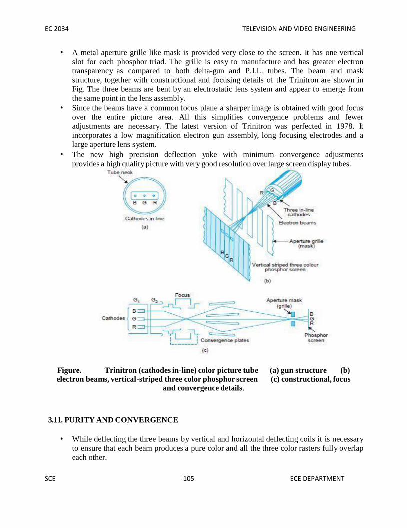
EC 2034 TELEVISION AND VIDEO ENGINEERING
SCE 105105105
ECE DEPARTMENT
A metal aperture grille like mask is provided very close to the screen. It has one verticalslot for each phosphor triad. The grille is easy to manufacture and has greater electrontransparency as compared to both delta-gun and P.I.L. tubes. The beam and maskstructure, together with constructional and focusing details of the Trinitron are shown inFig. The three beams are bent by an electrostatic lens system and appear to emerge fromthe same point in the lens assembly.
Since the beams have a common focus plane a sharper image is obtained with good focusover the entire picture area. All this simplifies convergence problems and feweradjustments are necessary. The latest version of Trinitron was perfected in 1978. Itincorporates a low magnification electron gun assembly, long focusing electrodes and alarge aperture lens system.
The new high precision deflection yoke with minimum convergence adjustmentsprovides a high quality picture with very good resolution over large screen display tubes.
Figure. Trinitron (cathodes in-line) color picture tube (a) gun structure (b)electron beams, vertical-striped three color phosphor screen (c) constructional, focus
and convergence details.
3.11. PURITY AND CONVERGENCE
While deflecting the three beams by vertical and horizontal deflecting coils it is necessaryto ensure that each beam produces a pure color and all the three color rasters fully overlapeach other.

EC 2034 TELEVISION AND VIDEO ENGINEERING
SCE 106106106
ECE DEPARTMENT
For obtaining color purity each beam should land at the center of the correspondingphosphor dot irrespective of the location of the beams on the raster. This needs precisealignment of the color beam and is carried out by a circular magnet assembly known asthe purity magnet.
It is mounted externally on the neck of the tube and close to the deflection yoke. Thepurity magnet assembly consists of several flat washer like magnets held together byspring clamps in such a way that these can be rotated freely.
The tabs on the magnets can be moved apart to reduce resultant field strength. This isillustrated for a two pole magnet in Fig.
As shown in the same figure, the tabs when moved together change the direction ofmagnetic field. Two, four and six pole magnet units are employed to achieve individualand collective beam deflections. Thus to affect purity and static convergence the beamscan be deflected up or down, right or left and diagonally by suitably orienting the puritymagnets.
Yoke Position The position of the yoke on the tube neck determines the location of the deflection centre
of the electron beams. A wrong setting will result in poor purity due to improper entryangles of the beams into the mask openings.
Since deflection due to yoke fields affects the landing of the beams on the screen moretowards the edges of the tube, the yoke is moved along the neck of the tube to improvepurity in those regions.
Convergence The technique of bringing the beams together so that they hit the same part of the screen
at the same time to produce three coincident rasters is referred to as convergence.Convergence errors are caused by (i) non-coincident convergence planes, (ii) nonuniformity of the deflection field and (iii) flat surface of the picture tube screen. Figureillustrates correct and incorrect convergence of beams.
Proper convergence is achieved by positional adjustment of the individual beams. It fallsinto two parts referred to as (i) static and (ii) dynamic convergence.
Static convergence involves movement of the beams by permanent magnetic fieldswhich, once correctly set, bring the beams into convergence in the central area of thescreen. Convergence over the rest of the screen is achieved by continuously varying(dynamic) magnetic fields, the instantaneous strengths of which depend upon thepositions of the spots on the screen.
These fields are set up by electromagnets which carry currents at horizontal(line) andvertical (field) frequencies. In practice convergence coils are often connected in serieswith respective yoke windings.

EC 2034 TELEVISION AND VIDEO ENGINEERING
SCE 107107107
ECE DEPARTMENT
Figure. Two pole purity magnet assembly (a) strong magnetic field when tabs (A and B) arenearly together (b) spreading the tabs reduces magnetic field (c) rotating the magnetstogether rotates the magnetic field to cause change in the direction of beam deflection
Purity and Static Convergence
Modern P.I.L. tubes are manufactured with such precision that hardly any purity andstatic convergence adjustments are necessary. However, to correct for small errors due tomounting tolerances and stray magnetic fields multi pole permanent magnet units areprovided.
Such a unit is mounted on the neck of the tube next to the deflection yoke. The variousmagnets are suitably oriented to achieve color purity, static convergence and straightnessof horizontal raster lines.
Convergence Errors
The need for the three rasters to be accurately superposed on each other with no east towest (lateral) or north to south (vertical) displacement (i.e., in proper color register) putsstringent constraints on distribution of the deflection field.
Non-optimum distribution of the field along with the fact that the screen is a nearly flatsurface (and not spherical) can produce two kinds of lack of color registration, commonlyknown as convergence errors.

EC 2034 TELEVISION AND VIDEO ENGINEERING
These are (a) astigmatism and (b) coma effects.(a) Astigmatism. As shown in Fig. (a),with a uniform field the rays from a vertical row of points (P, G, Q) converge short of thescreen producing a vertical focal line on the screen. However, rays (R, G, B) from a rowof horizontal points converge beyond the screen producing a horizontal line on thescreen.
Such an effect is known as astigmatism and causes convergence errors. In the case of aP.I.L. tube, beams R, G and B emerge only from a horizontal line and so any verticalastigmatism will have no effect. However, if horizontal astigmatism is to be avoided, thehorizontal focus must be a point on the screen and not a line for any deflection.
A given change in the shape of the deflection field produces opposite changes in verticaland horizontal astigmatic effects. Since vertical astigmatism is of no consequence in a P-I-L tube, suitable field adjustments can be made to ensure that the beams coming from in-line guns in a horizontal line converge at the same point on the screen irrespective of thedeflection angle. Such a correction will however, be at the cost of a much larger verticalastigmatism but as stated above it does not interfere with the correct registration ofvarious colors.(b) Coma Effect.
Due to non-uniformity of the deflection field all the beams are not deflected by the sameamount. As shown in Fig (b) the central beam (green) deflects by a smaller amount ascompared to the other two beams.
For a different non-uniformity of the deflection field, the effect could be just oppositeproducing too large a displacement of the central beam. Such a distortion is known ascoma and results in mis-convergence of the beams.
SCE 108 ECE DEPARTMENT

EC 2034 TELEVISION AND VIDEO ENGINEERING
SCE 109109109
ECE DEPARTMENT
Figure. Astigmatism in a uniform deflection field
Figure. The coma effect—central beam deflection less (or more) than the side beams
Field Distribution for Optimum Convergence
In order to correct astigmatic and coma effects different field configurations arenecessary. To help understand this, it is useful to visualize the deflection field in roughlytwo parts, the half of it closer to the screen and the other half closer to the guns.
Astigmatism is caused by only that part of the field which is closer to the screen whereascoma effects occur due to non uniformities of the field all over the deflection area. Tocorrect for mis convergence due to astigmatism in a P.I.L. tube the horizontal deflectionfield must be pincushion shaped and the vertical deflection field barrel shaped (Fig.) inthe half near the screen.
But such a field configuration produces undue amounts of coma error. To circumventthis, the gun end of the field can be modified in such a way that the coma produced by thescreen end field is just neutralized, thus giving a scan that is free from all convergenceerrors.
This needs that the field distribution at the gun end be barrel shaped horizontally andpincushion vertically. The above two requirements are illustrated in Fig. (b) which showsnecessary details of horizontal and vertical field distributions relative to each other alongthe axis of the tube.
Though complicated, the above constraints of field distribution are met by properdeflection coil design and thus both astigmatic and coma effects are eliminated.

EC 2034 TELEVISION AND VIDEO ENGINEERING
SCE 110110110
ECE DEPARTMENT
Figure. Field configurations (i) pincushion horizontal deflection field (ii) barrel shapedvertical deflection field
Figure. Quantitative visualization of deflection field distribution for astigmatism and comacorrections in a P-I-L picture tube.
DYNAMIC CONVERGENCE ADJUSTMENTS The display unit consisting of picture tube and deflection unit is inherently self-
converging. However, small adjustments become necessary and are provided. For thispurpose two types of four-pole dynamic magnetic fields are used.
One is generated by additional windings on the yoke ring of the deflection unit. It isenergized by adjustable sawtooth currents synchronized with scanning. The other type ofdynamic field is generated by sawtooth and parabolic currents which are synchronizedwith scanning and flow through the deflection coils. (i) Line symmetry. Figure (a) showsa situation in which the plane where the beams are converged automatically is slightlytilted with respect to the screen plane due to some small left-right asymmetry in thedistribution of the horizontal deflection field.
As a result, horizontal convergence errors of opposite signs occur at the sides of thescreen. The same type of error can be caused by a horizontal deviation of the un deflected

EC 2034 TELEVISION AND VIDEO ENGINEERING
beams from the screen center. As shown in Fig. (b) such an error can be corrected by a 4-pole field aligned diagonally with respect to the deflection fields. This field is generatedby driving a sawtooth current at line frequency through an additional four-pole windingprovided around the core of the deflection yoke.
The sawtooth current is obtained directly from the line deflection circuit. (ii) Fieldsymmetry. As illustrated in Fig. vertical displacement of the plane of the beams withrespect to the center of the vertical deflection causes horizontal convergence errors duringvertical deflection.
These errors can be corrected by feeding a rectified sawtooth current at field frequencythrough the additional 4-pole winding on the deflection unit. (iii) Line balance. Verticaldisplacement of the plane of beams with respect to center of the horizontal deflectionfield causes cross-over of the horizontal red and blue lines.
This illustrated in Fig. The same type of error can also be caused by top-bottomasymmetry of the horizontal deflection field. It can be corrected by a four-pole fieldwhich is aligned orthogonally with respect to the deflection fields.
Such a field is generated by unbalancing (see corresponding figures) the line deflectioncurrent through the two halves of the horizontal deflection coils acted with respect to itsnormal orientation, a parabolic vertical convergence error occurs during both horizontaland vertical deflection (Fig.).
This error can be corrected by feeding a parabolic current at line frequency through theline deflection coils.(v) Field balance at top and bottom. Left-right asymmetry of thevertical deflection field or horizontal deviation of the un-deflected beams from the screencenter causes vertical convergence errors during vertical deflection.
This is illustrated (Fig) separately for top and bottom of the screen. The correction at thetop is made by unbalancing the field deflection coils during the first-half of the field scan.Similarly correction at the bottom is made by unbalancing the field deflection coilsduring the second-half of the field scan.
Figure. Horizontal convergence errors.
SCE 111 ECE DEPARTMENT

EC 2034 TELEVISION AND VIDEO ENGINEERING
Figure. Line symmetry correction (horizontal red-to-blue distance) at the ends ofhorizontal axis.
Figure. Field symmetry. Red-blue cross-over of the vertical lines cause horizontalconvergence errors at the ends of vertical axis.
SCE 112 ECEDEPARTMENT

EC 2034 TELEVISION AND VIDEO ENGINEERING
Figure. Red-blue cross-overof horizontal lines
causes vertical convergenceerrors at the end of horizontal axis.
Figure. Rotation of electron beams causes vertical convergence errors of a parabolic nature
SCE 113 ECE DEPARTMENT
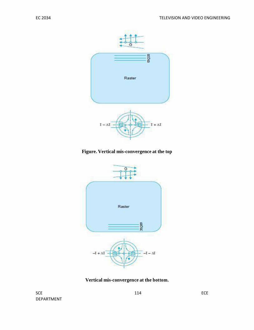
EC 2034 TELEVISION AND VIDEO ENGINEERING
Figure. Vertical mis-convergence at the top
Vertical mis-convergence at the bottom.
SCE 114 ECEDEPARTMENT
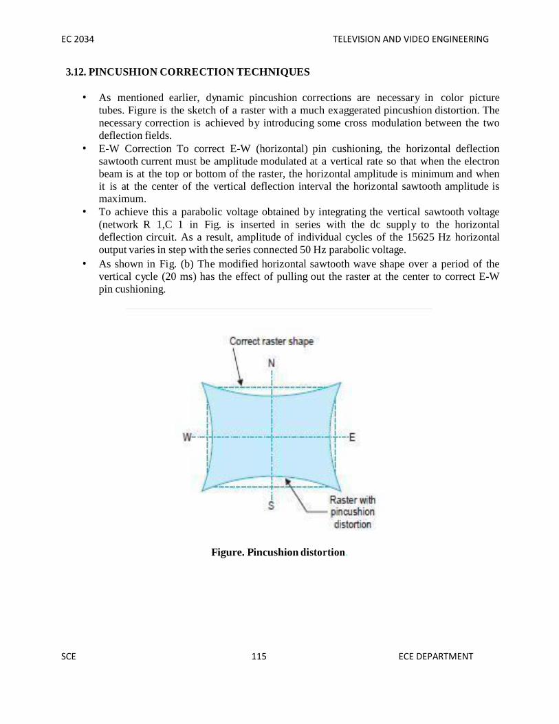
EC 2034 TELEVISION AND VIDEO ENGINEERING
SCE 115115115
ECE DEPARTMENT
3.12. PINCUSHION CORRECTION TECHNIQUES
As mentioned earlier, dynamic pincushion corrections are necessary in color picturetubes. Figure is the sketch of a raster with a much exaggerated pincushion distortion. Thenecessary correction is achieved by introducing some cross modulation between the twodeflection fields.
E-W Correction To correct E-W (horizontal) pin cushioning, the horizontal deflectionsawtooth current must be amplitude modulated at a vertical rate so that when the electronbeam is at the top or bottom of the raster, the horizontal amplitude is minimum and whenit is at the center of the vertical deflection interval the horizontal sawtooth amplitude ismaximum.
To achieve this a parabolic voltage obtained by integrating the vertical sawtooth voltage(network R 1,C 1 in Fig. is inserted in series with the dc supply to the horizontaldeflection circuit. As a result, amplitude of individual cycles of the 15625 Hz horizontaloutput varies in step with the series connected 50 Hz parabolic voltage.
As shown in Fig. (b) The modified horizontal sawtooth wave shape over a period of thevertical cycle (20 ms) has the effect of pulling out the raster at the center to correct E-Wpin cushioning.
Figure. Pincushion distortion.

EC 2034 TELEVISION AND VIDEO ENGINEERING
SCE 116116116
ECE DEPARTMENT
N-S Correction
The top and bottom or N-S pincushion correction is provided by forcing the verticalsawtooth current to pulsate in amplitude at the horizontal scanning rate. During top andbottom scanning of the raster a parabolic waveform at the horizontal rate is superimposedon the vertical deflection sawtooth.
In fact this increases vertical size during the time the beam is moving through themidpoint of its horizontal scan. The parabolic waveform at the top of the raster is ofopposite polarity to that at the bottom since the raster stretch required at the top isopposite to the needed at the bottom.
The amplitude of the parabolic waveform required for top and bottom pincushioncorrection decreases to zero as vertical deflection passes through the centre of the raster.
Figure. Vertical (N – S) pincushion correction circuit and waveforms.

EC 2034 TELEVISION AND VIDEO ENGINEERING
SCE 117117117
ECE DEPARTMENT
3.13. AUTOMATIC DEGAUSSING (ADG) CIRCUIT
There are many degaussing circuits in use. Figure shows details of a popular automaticdegaussing circuit. It uses a thermistor and a varistor for controlling the flow ofalternating current through the degaussing coil.
When the receiver is turned on the ac voltage drop across the thermistor is quite high(about 60 volts) and this causes a large current to flow through the degaussing coil.Because of this heavy current, the thermistor heats up, its resistance falls and voltagedrop across it decreases.
As a result, voltage across the varistor decreases thereby increasing its resistance. This inturn reduces ac current through the coil to a very low value. The circuit components areso chosen that initial surge of current through the degaussing coil is close to 4 amperesand drops to about 25 mA in less than a second.
This is illustrated in Fig. Once the thermistor heats up degaussing ends and normal acvoltage is restored to the B + rectifier circuit.
Figure. Automatic degaussing (ADG) (a) typical circuit (b) variation of current in thedegaussing coil when receiver is just switched on.
3.14. GREY SCALE TRACKING
It may be recalled that red, green and blue lights must combine in definite proportions toproduce white light. The three phosphors have different efficiencies. Also the three gunsmay not have identical I p /V gk characteristics and cut-off points.
Therefore, it becomes necessary to incorporate suitable adjustments such thatmonochrome information is reproduced correctly (with no color tint) for all settings ofthe contrast control. In practice, this amounts to two distinct steps:

EC 2034 TELEVISION AND VIDEO ENGINEERING
SCE 118118118
ECE DEPARTMENT
(a) Adjustment of Low Lights Non-concident I p /V gk characteristics and consequent difference in cut-off points of the
three guns, results in appearance of colored tint instead of pure dark grey shades in areasof low brightness. To correct this it is necessary to bring the cut-off points in coincidence.This is achieved by making the screen grid (i.e., 1st anode) voltage different from eachother. Potentiometers are normally provided for this purpose in the dc voltage supply tothe three screen grids.
(b) Adjustment of High Lights It is equally necessary to ensure that all other levels of white are also correctly
reproduced.This amounts to compensating for the slightly different slopes and also forthe substantially different phosphor efficiencies.
This is achieved by varying the video (luminance) signal drive to the three guns. Sincethe red phosphor has the lowest efficiency, maximum video signal is fed to the redcathode and then by the use of potentiometers video signal amplitudes to the green andblue guns are varied (see Fig.) to obtain optimum reproduction of high lights
3.15. COLOR SIGNAL TRANSMISSION
The color video signal contains two independent information, that of hue and saturation.It is a difficult matter to modulate them to one and the same carrier in such a way thatthese can be easily recovered at the receiver without affecting each other.
The problem is accentuated by the need to fit this color signal into a standard TV channelwhich is almost fully occupied by the ‘Y’ signal. However, to satisfy compatibilityrequirements the problem has been ingeniously solved by combining the colorinformation into a single variable and by employing what is known as frequencyinterleaving.
(In the CCIR PAL I standards the picture and sound carrier are 6 MHz apart and the channelbandwidth is 8 MHz. The only difference between PAL-B and PAL-G is in the channelbandwidth)
PAL-B with channel bandwidth of 7 MHz does not provide any inter-channel gap,whereas PAL-G with channel bandwidth of 8 MHz provides a band gap of 1 MHz in-between successive channels.

EC 2034 TELEVISION AND VIDEO ENGINEERING
SCE 119119119
ECE DEPARTMENT
Figure. Interleaving of the color signal.
3.15. COLOR SIGNAL TRANSMISSION AND RECEPTION
Frequency interleaving in television transmission is possible because of the relationshipof the video signal to the scanning frequencies which are used to develop it. It has beendetermined that the energy content of the video signal is contained in individual energy‘bundles’ which occur at harmonics of the line frequency (15.625, 31.250 ... KHz) thecomponents of each bundle being separated by a multiplier of the field frequency (50,100, ... Hz).
The shape of each energy bundle shows a peak at the exact harmonics of the horizontalscanning frequency. This is illustrated in Fig. As shown there, the lower amplitudeexcursions that occur on either side of the peaks are spaced at 50 Hz intervals andrepresent harmonics of the vertical scanning rate.

EC 2034 TELEVISION AND VIDEO ENGINEERING
SCE 120120120
ECE DEPARTMENT
The vertical sidebands contain less energy than the horizontal because of the lower rate ofvertical scanning. Note that the energy content progressively decreases with increase inthe order of harmonics and is very small beyond 3.5 MHz from the picture carrier.
It can also be shown that when the actual video signal is introduced between the line syncpedestals, the overall spectra still remains ‘bundled’ around the harmonics of the linefrequency and the spectrum of individual bundles become a mixture of continuousportion due to the video signal are discrete frequencies due to the field sync as explainedearlier.
Therefore, a part of the bandwidth in the monochrome television signal goes unusedbecause of spacing between the bundles. This suggests that the available space could beoccupied by another signal. It is here where the color information is located bymodulating the color difference signals with a carrier frequency called ‘color subcarrier’.The carrier frequency is so chosen that its sideband frequencies fall exactly mid-waybetween the harmonics of the line frequency.
This requires that the frequency of the subcarrier must be an odd multiple of half the linefrequency. The resultant energy clusters that contain color information are shown in Fig.by dotted chain lines along with the Y signal energy bands. In order to avoid crosstalkwith the picture signal, the frequency of the subcarrier is chosen rather on the high side ofthe channel bandwidth.
It is 567 times one-half the line frequency in the PAL system. This comes to: (2 × 283 +1) 15625/2 = 4.43 MHz. Note that in the American 525 line system, owing to smallerbandwidth of the channel, the subcarrier employed is 455 times one-half the linefrequency i.e., (2 × 227 + 1) 15750/2 and is approximately equal to 3.58 MHz.
3.16. BANDWIDTH FOR COLOR SIGNAL TRANSMISSION
The Y signal is transmitted with full frequency bandwidth of 5 MHz for maximumhorizontal details in monochrome. However, such a large frequency spectrum is notnecessary for color video signals.
The reason being, that for very small details, the eye can perceive only the brightness butnot the color. Detailed studies have shown that perception of colors by the human eye,which are produced by combinations of the three primary colors is limited to objectswhich have relatively large colored areas (≈ 1/25th of the screen width or more). Onscanning they generate video frequencies which do not exceed 0.5 MHz. Further, formedium size objects or areas which produce a video frequency spectrum between 0.5 and1.5 MHz, only two primary colors are needed.
This is so, because for finer details the eye fails to distinguish purple (magenta) andgreen-yellow hues from greys. As the colored areas become very small in size (width),the red and cyan hues also become indistinguishable from greys.
Thus for very fine color details produced by frequencies from 1.5 MHz to 5 MHz, allpersons with normal vision are color bling and see only changes in brightness even forcolored areas.
Therefore, maximum bandwidth necessary for color signal transmission is around 3 MHz(± 1.5 MHz).

EC 2034 TELEVISION AND VIDEO ENGINEERING
SCE 121121121
ECE DEPARTMENT
Figure. Quadrature amplitude modulated color difference signals and the position ofresultant subcarrier phasor for the primary and complementary colors. Note that themagnitudes shown correspond to unweighted values of color difference signals.
EC 2034 TELEVISION AND VIDEO ENGINEERING
SCE 122122122
ECE DEPARTMENT
MODULATION OF COLOR DIFFERENCE SIGNALS
The problem of transmitting (B-Y) and (R-Y) video signals simultaneously with onecarrier frequency is solved by creating two carrier frequencies from the same colorsubcarrier without any change in its numerical value.
Two separate modulators are used, one for the (B-Y) and the other for the (R-Y) signal.However, the carrier frequency fed to one madulator is given a relative phase shift of 90°with respect to the other before applying it to the modulator.
Thus, the two equal subcarrier frequencies which are obtained from a common generatorare said to be in quadrature and the method of modulation is known as quadraturemodulation.
After modulation the two outputs are combined to yield C, the resultant subcarrierphasor. Since the amplitude of C, the chrominance signal, corresponds to the magnitudesof color difference signals, its instantaneous value represents color saturation at thatinstant.
Maximum amplitude corresponds to greatest saturation and zero amplitude to nosaturation i.e., white. Similarly, the instantaneous value of the C phasor angle (θ) whichmay vary from 0° to 360° represents hue of the color at that moment.
Thus the chrominance signal contains full information about saturation and hue ofvarious colors. This being a crucial point in color signal transmission, is illustrated by afew examples. However, it would be necessary to first express (R-Y) and (B-Y) in termsof the three camera output voltages.
This is done by substituting Y = 0.59G + 0.3R + 0.11B in these expressions. Thus (R-Y) becomes R – 0.59G – 0.3R – 0.11B = 0.7R – 0.59G – 0.11B. Similarly, (B-Y) becomes B – 0.59G – 0.3R – 0.11B = 0.89B – 0.59G – 0.3R. Now suppose that only pure red color is being scanned by the color camera. This would
result in an output from the red camera only, while the green and blue outputs will bezero. Therefore, (R-Y) signal will become simply + 0.7R and (B-Y) signal will bereduced to – 0.3R.
The resultant location of the subcarrier phasor after modulation is illustrated in Fig. Notethat the resultant phasor is counter clockwise to the position of + (R-Y) phasor. Nextconsider that the color camera scans a pure blue color scene.
This yields (R-Y)= – 0.11B and (B-Y) = 0.89 B. The resultant phasor for this color lags +(B-Y) vector by a small angle. Similarly the location and magnitude for any color can befound out. This is illustrated in Fig. for the primary and complementary colors.
Another point that needs attention is the effect of desaturation on the color phasors. Sincedesaturation results in reduction of the amplitudes of both (B-Y) and (R-Y) phasors, theresultant chrominance phasor accordingly changes its magnitude depending on the degreeof de-saturation.
Thus any change in the purity of a color is indicated by a change in the magnitude of theresultant subcarrier phasor. Color Burst Signal Suppressed carrier double sidebandworking is the normal practice for modulating color- difference signals with the colorsubcarrier frequency.

EC 2034 TELEVISION AND VIDEO ENGINEERING
This is achieved by employing balanced modulators. The carrier is suppressed tominimize interference produced by the chrominance signals both on monochromereceivers when they are receiving color transmissions and in the luminance channel ofcolor receivers themselves. As explained in an earlier chapter the ratio of the sidebandpower to carrier power increases with the depth of modulation.
However, even at 100% modulation two-thirds of the total power is in the carrier andonly one-third is the useful sideband power. Thus suppressing the carrier clearlyeliminates the main potential source of interference.
In addition of this, the color-difference signals which constitute the modulatinginformation are zero when the picture detail is non-colored (i.e., grey, black or whiteshades) and so at such times the sidebands also disappear leaving no chrominancecomponent in the video signal.
As explained above the transmitted does not contain the subcarrier frequency but it isnecessary to generate it in the receiver with correct frequency and phase relationship forproper detection of the color sidebands.
To ensure this, a short sample of the subcarrier oscillator, 8 to 11 cycles) called the ‘colorburst’ is sent to the receiver along with sync signals. This is located in the back porch ofthe horizontal blanking pedestal.
The color burst does not interfere with the horizontal sync because it is lower inamplitude and follows the sync pulses. Its exact location is shown in Fig.
The color burst is gated out at the receiver and is used in conjunction with a phasecomparator circuit to lock the local subcarrier oscillator frequency and phase with that atthe transmitter.
As the burst signal must maintain a constant phase relationship with the scanning signalsto ensure proper frequency interleaving, the horizontal and vertical sync pulses are alsoderived from the subcarrier through frequency divider circuits.
Figure. Location of color burst on the back porch of each horizontal sync pulse.
SCE 123 ECE DEPARTMENT

EC 2034 TELEVISION AND VIDEO ENGINEERING
3.17. WEIGHTING FACTORS
The resultant chrominance signal phasor (C) is added to the luminance signal (Y) beforemodulating it with the channel carrier for transmission. The amplitude, i.e., level line ofY signal becomes the zero line for this purpose.
Such an addition is illustrated in Fig. for a theoretical 100 percent saturated, 100 percentamplitude color bar signal. The peak-to-peak amplitude of green signal (± 0.83) getsadded to the corresponding luminance amplitude of 0.59.
For the red signal the chrominance amplitude of ± 0.76 adds to its brightness of0.3.Similarly other colors add to their corresponding luminance values to form thechroma signal.
However, observe that it is not practicable to transmit this chroma waveform because thesignal peaks would exceed the limits of 100 percent modulation. This means that onmodulation with the picture carrier some of the color signal amplitudes would exceed thelimits of maximum sync tips on one side and white level on the other.
For example, in the case of magenta signal, the chrominance value of ± 0.83 when addedto its luminance amplitude of 0.41 exceeds the limits of 100 percent modulation of bothwhite and black levels.
Similarly blue signal amplitude greatly exceeds the black level and will cause a highdegree of over modulation. If over modulation is permitted the reproduced colors will getobjectionably distorted.
Therefore, to avoid over modulation on 100 percent saturation color values, it isnecessary to reduce the amplitude of color difference video signal before modulatingthem with the color subcarrier. Accordingly, both (R–Y) and (B–Y) components of thecolor video signal are scaled down by multiplying them with what are known as‘weighting factors’.
Those used are 0.877 for the (R–Y) component and 0.493 for the (B–Y) component. Thecompensated values are obtained by using potentiometers at the outputs of (R–Y) and(B–Y) adders (see Fig.).
Note that no reduction is made in the amplitude of Y signal. It may also be noted thatsince the transmitter radiates weighted chrominance signal values, these must beincreased to the uncompensated values at the color TV receiver for proper reproductionof different hues.
This is carried out by adjusting gains of the color difference signal amplifiers. The unweighted and weighted values of color difference signals are given below in Table.
SCE 124 ECE DEPARTMENT

EC 2034 TELEVISION AND VIDEO ENGINEERING
SCE 125 ECE DEPARTMENT

EC 2034 TELEVISION AND VIDEO ENGINEERING
SCE 126 ECEDEPARTMENT
EC 2034 TELEVISION AND VIDEO ENGINEERING
Generation of composite color signal for a theoretical 100% saturated, 100% amplitudecolor bar signal. As seen from the relative amplitude scales, the composite video signalwould cause gross over-modulation. Therefore in practice the color difference signals arereduced in amplitude to avoid any excessive over-modulation
3.18. FORMATION OF THE CHROMINANCE SIGNAL
Using the information of Table, Fig. illustrates the formation of the chroma signal for acolor bar pattern after the color difference signals have been scaled down in accordancewith corresponding weighting factors.
Note that new amplitudes of the chrominance subcarrier signals are 0.63 for red and cyan,0.59 for green and magenta and 0.44 for blue and yellow.
These amplitudes will still cause over modulation to about 33%. This is permitted,because in practice, the saturation of hues in natural and staged scenes seldom exceeds 75percent.
Since the amplitude of chroma signal is proportional to the saturation of hue, maximumchroma signal amplitudes are seldom encountered in practice.
Therefore, the weighted chroma values result in a complete color signal that will rarely, ifever, over modulate the picture carrier of a CTV transmitter. Hence it is not necessary tofurther decrease the signal amplitudes by employing higher weighting factors.
Chroma Signal Phasor Diagram
The compensation (readjustment) of chroma signal values results in a change of chromaphase angles. In the NTSC system it is a common practice to measure phase anglesrelative to the – (B–Y) phasor.
This location has been designated 0° or the reference phase position on the phasordiagram (see Fig.) because this is also the phase of the color burst that is transmitted onthe back porch of each horizontal sync pulse.
Referring to Fig. the compensated color magenta is represented by a phasor at an angle of119°. In the same manner the diagram indicates phase angles and amplitudes of othercolor signals. Note that primary colors are 120° apart and complementary colors differ inphase by 180° from their corresponding primary colors.
SCE 127 ECE DEPARTMENT

EC 2034 TELEVISION AND VIDEO ENGINEERING
100% saturated, 100% amplitude color-bar signal in which the color difference signalsare reduced by weighting factors to restrict the chrominance signal excursions to 33%beyond black and peak white levels.
SCE 128 ECE DEPARTMENT

EC 2034 TELEVISION AND VIDEO ENGINEERING
Figure. Magnitude and phase relationships of compensated chrominance signals for theprimary and complementary colors.
SCE 129 ECE DEPARTMENT

EC 2034 TELEVISION AND VIDEO ENGINEERING
UNIT IV
COLOUR TELEVISION SYSTEMS
4.1. NTSC COLOUR TV SYSTEM
The NTSC colour system is compatible with the American 525 line monochrome system.In order to save bandwidth, advantage is taken of the fact that eye’s resolution of coloursalong the reddish blue-yellowish green axis on the colour circle is much less than thosecolours which lie around the yellowish red-greenish blue axis.
Therefore two new colour video signals, which correspond to these colour regions, aregenerated.
These are designated as I and Q signals.The I signal lies in a region 33° counterclockwise to + (R – Y) where the eye has maximum colour resolution. It* is derived fromthe (R – Y) and (B – Y) signals and is equal to 0.60R – 0.28G – 0.32B.
As shown in Fig. it is located at an angle of 57° with respect to the colour burst in thebalanced modulator circuits. Similarly the Q** signal is derived from colour differencesignals by suitable matrix and equals 0.21R –0.52G + 0.31B. It is located 33° counterclockwise to the +(B – Y) signal and is thus in quadrature with the I signal.
As illustrated in Fig. the Q signal covers the regions around magenta (reddish-blue) andyellow-green shades.
Similarly orange hues correspond to phase angles centred around + I and the
I = 0.74(R – Y) – 0.27(B – Y).
Q = 0.48(R – Y) + 0.41(B – Y).
complementary blue-green (cyan) hues are located around the diametrically opposite – Isignal.Since the eye is capable of resolving fine details in these regions, I signal isallowed to possess frequencies up to 1.5 MHz.
However, the eye is least sensitive to colours that lie around the ±Q signals, and thereforeit is allowed a bandwidth of only ±0.5 MHz with respect to the colour subcarrier.
SCE 130 ECE DEPARTMENT

EC 2034 TELEVISION AND VIDEO ENGINEERING
SCE 131131131
ECE DEPARTMENT
Figure. Phasor diagrams of the I and Q signals in the NTSC system.
It may be noted that both I and Q signals are active up to 0.5 MHz and being at rightangles to each other, combine to produce all the colours contained in the chrominancesignal.
However, the Q signal drops out after 0.5 MHz and only I signal remains between 0.5and 1.5 MHz to produce colours, the finer details of which the eyes can easily perceive.
To help understand this fact it may be recalled that only one colour difference signal isneeded for producing colours which are a mixture of only two colours. Thus the Q signalis not necessary for producing colours lying in the region of orange (red + green) andcyan (green +blue) hues.
Hence at any instant when Q = 0 and only I signal is active the colours produced on thescreen will run the gamut from reddish orange to bluish green.Bandwidth ReductionDouble sideband transmission is allowed for the Q signal and it occupies a channelbandwidth of 1 MHz (± 0.5 MHz). However, for the I signal the upper sideband isrestricted to a maximum of 0.5 MHz while the lower sideband is allowed to extent up to1.5 MHz. As such it is a form of vestigial sideband transmission.
Thus in all, a bandwidth of 2 MHz is necessary for colour signal transmission. This is asaving of 1 MHz as compared to a bandpass requirement of 3 MHz if (B – Y) and (R –Y) are directly transmitted.It is now obvious that in the NTSC system, advantage is takenof the limitations of the human eye to restrict the colour signal bandwidth, which in turnresults in reduced interference with the sound and picture signal sidebands.

EC 2034 TELEVISION AND VIDEO ENGINEERING
SCE 132132132
ECE DEPARTMENT
The reduction in colour signal sidebands is also dictated by the relatively narrow channelbandwidth of 6 MHz in the American TV system.
Exact Colour Subcarrier Frequency The colour subcarrier frequency in the NTSC systemhas been chosen to have an exact value equal to 3.579545 MHz. The reason for fixing itwith such a precision is to maintain compatibility between monochrome and coloursystems.
Any interference between the chrominance signal and higher video frequencies isminimized by employing suppressed carrier (colour subcarrier) transmission and by usinga notch filter in the path of the luminance signal. However, when a colour transmission isreceived on a monochrome receiver a dot pattern structure appears along each raster lineon the receiver screen.
This is caused by the colour signal frequencies that lie within the pass-band of the videosection of the receiver. As illustrated below such an interference can be eliminated if thesubcarrier frequency is maintained at the exact value mentioned above. Assume that theinterfering colour signal has a sinusoidal variation which rides on the average brightnesslevel of the monochrome signal.
This produces white and black dots on the screen. If the colour subcarrier happens to be amultiple of the line frequency (n × f h ) the phase position of the disturbing colourfrequency will be same on successive even or odd fields. Thus black and white dots willbe produced at the same spots on the screen and will be seen as a persistent dot patterninterference.
However, if a half-line offset is provided by fixing the sub- carrier frequency to be an oddmultiple of the half-line frequency, the disturbing colour signal frequency will haveopposite polarity on successive odd and even fields. Thus as the same spot on the displayscreen a bright dot image will follow a dark one alternately.
The cumulative effect of this on the eye would get averaged out and the dot pattern willbe suppressed. As an illustration of this phenomenon assume that a simple five linescanning system is being used. Figure shows the effect of sinewave luminance signal thatis an odd harmonic of one-half of the scanning frequency.
Each negative excursion of the signal at the cathode of the picture tube will produce aunit area of brightness on the screen while the positive going excursions of the signal willcause unit dark areas on the picture.
In the illustration under consideration where the sinewave completes 3.5 cycles duringone active horizontal line, four dark areas and three areas of brightness will be producedduring the first line scan. Because of the extra half-cycle the next horizontal scan begins
EC 2034 TELEVISION AND VIDEO ENGINEERING
SCE 133133133
ECE DEPARTMENT
with an area of brightness and the entire line contains only three dark areas. the same off-set occurs on each succeeding line, producing a checkerboard pattern on the screen.
Since the scanning rate in the example utilizes an odd number of horizontal scans foreach complete presentation, the luminance signal will be 180° out of phase with theprevious signal as line number one is again scanned. Thus the pattern obtained on thescreen will be the reverse of that which was generated originally.
The total effect of the above process on the human eye is one of cancellation. Since inactual practice scanning takes place at a very fast rate, the presistency of the eye blendsthe patterns together with the effect that visibility of the dot structure is considerablyreduced and goes unnoticed on a monochrome receiver.
The compatibility considerations thus dictate that the colour sub-carrier frequency (f sc )should be maintained at 3.583125, i.e., (2 × 227 + 1) × 15750/2 MHz.
However, the problem does not end here, because the sound carrier and the colour sub-carrier beat with each other in the detector and an objectionable beat note of 0.92 MHz isproduced (4.5 – 3.58 = 0.92).
This interferes with the reproduced picture. In order to cancel its cumulative effect it isnecessary that the sound carrier frequency must be an exact multiple of an even harmonicof the line frequency.
The location of the sound carrier at 4.5 MHz away from the picture carrier cannot bedisturbed for compatibility reasons and so 4.5 MHz is made to be the 286th harmonic ofthe horizontal deflection frequency. Therefore, f h = 4.5 MHz / 286 = 15734.26 Hz ischosen.
Note that this is closest to the value of 15750 Hz used for horizontal scanning formonochrome transmission.
A change in the line frequency necessitates a in the field frequency since 262.5 linesmust be scanned per field. Therefore the field frequency (f v ) is changed to be15734.26/262.5 = 59.94 Hz in place of 60 Hz.
The slight difference of 15.74 Hz in the line frequency (15750 – 15734.26 = 15.74 Hz)and of 0.06 Hz in the field frequency (60 – 59.94 = 0.06 Hz) has practically no effect onthe deflection oscillators because an oscillator that can be triggered by 60 Hz pulses canalso be synchronized to produce 59.94 Hz output.
Similarly the AFC circuit can easily adjust the line frequency to a slightly different valuewhile receiving colour transmission.
EC 2034 TELEVISION AND VIDEO ENGINEERING
SCE 134134134
ECE DEPARTMENT
As explained earlier the colour sub-carrier frequency must be an odd multiple of half theline frequency to suppress dot pattern interference. Therefore f sc is fixed at (2n + 1) f h/2, i.e., 455 × 15734.26/2 = 3.579545 MHz.
To obtain this exact colour sub-carrier frequency, a crystal controlled oscillator isprovided. Encoding of Colour Picture Information Figure illustrates the encondingprocess of colour signals at the NTSC transmitter.
A suitable matrix is used to get both I and Q signals directly from the three cameraoutputs. Since I = 0.60R – 0.28G – 0.32B, the green and blue camera outputs are invertedbefore feeding them to the appropriate matrix. Similarly for Q = 0.21R – 0.52G + 0.31B,in invertor is placed at the output of green camera before mixing it with the other twocamera outputs. anced modulators.
The subcarrier to the I modulator is phase shifted 57° clockwise with respect to the colourburst. The carrier is shifted by another 90° before applying it to the Q modulator. Thusrelative phase shift of 90° between the two subcarriers is maintained for quadratureamplitude modulation.
It is the characteristic of a balanced modulator that while it suppresses the carrier andprovides frequency translation, both the amplitude and phase of its output are directlyrelated to the instantaneous amplitude and phase of the modulating signal.
Thus, with the subcarrier phase angles shifted to the locations of I and Q, the outputsfrom both the modulators retain full identity of the modulating colour difference signals.The sideband restricted output fromthe I modulator combines with the output of Qmodulator to form the chrominance signal. It is then combined with the composite Ysignal and colour burst in an adder to form composite chrominance signal. The outputfrom the adder feeds into the main transmitter and modulates the channel picture carrierfrequency. Note that colour subcarrier has the same frequency (3.579545 MHz) for all thestations whereas the assigned picture carrier frequency is different for each channel. Asimplified block diagram of the NTSC colour receiver is shown in Fig.. The signal fromthe selected channel is processed in the usual way by the tuner, IF and video detectorstages. The sound signal is separately detected, demodulated and amplified beforefeeding it to the loudspeaker. Similarly AGC, sync separator and deflection circuits havethe same form as in monochrome receivers except for the inclusion of purity,convergence and pincushion correction circuits. At the output of video detector thecomposite video and chrominance signals reappear in their original premodulated form.The Y signal is processed as in a monochrome receiver except that the video amplifierneeds a delay line. The delay line introduces a delay of about 500 ns which is necessaryto ensure time coincidence of the luminance and chroma signals because of the restrictedbandwidth of the latter.

EC 2034 TELEVISION AND VIDEO ENGINEERING
SCE 135135135
ECE DEPARTMENT
Decoding of the Chroma (C) Signal
The block diagram of Fig. shows more details of the colour section of the receiver. Thechroma signal is available along with other components of the composite signal at theoutput of the video preamplifier.
It should be noted that the chrominance signal has colour information during active tracetime of the picture and the burst occurs during blanking time when there is no picture.Thus, although the ‘C’ signal and burst are both at 3.58 MHz, they are not present at thesame time.
Chrominance Bandpass Amplifier
The purpose of the bandpass amplifier is to separate the chrominance signal from thecomposite video signal, amplify it and then pass it on to the synchronous demodulators.The amplifier has fixed tuning with a bandpass wide enough ( ≈ 2 MHz) to pass thechroma signal. The colour burst is prevented from appearing at its output by horizontalblanking pulses which disable the bandpass amplifier during the horizontal blankingintervals. The blanking pulses are generally applied to the colour killer circuit which isturn biases-off the chrominance amplifier during these periods.
Colour Demodulators
Synchronous demodulators are used to detect the molulating signal. Such a demodulatormay be thought of as a combination of phase and amplitude detectors because the outputis dependent on both phase and amplitude of the chroma signal. As shown in the blockdiagram (Fig) each demodulator has two input signals, the chroma which is to bedemodulated and a constant amplitude output from the local subcarrier oscillator. Theoscillator output is coupled to the demodulators by phase-shifting networks. The Idemodulator oscillator voltage has a phase of 57° with respect to the burst phase (f sc ∠0°) and so has the correct delay to detect the I colour difference signal. Similarly theoscillator voltage to the Q demodulator is delayed by 147° (57° + 90°) for detecting the Qcolour-difference signal. Thus the I and Q synchronous demodulators convert the chromasignal (a vector quantity) into its right-angle components (polar to rectangularconversion).
The Colour Matrix
This matrix is designed to produce (R – Y), (G – Y) and (B – Y) signals from the I and Qvideo signals. Colour difference signal amplifiers are required to perform two functions.While amplifying the signals they also compensate for the chroma signal compression(weighting factors) that was introduced at the transmitter as a means of preventingovermodulation.
The (R – Y) amplifier provides a relative boost of 1.14 = 1/87.7% while the (B – Y)amplifier does so by a factor of 2.03 = 1/49%. Similarly the (G – Y) amplifier reduces itsoutput level to become 0.7(70%) in a relative sense.

EC 2034 TELEVISION AND VIDEO ENGINEERING
SCE 136136136
ECE DEPARTMENT
The grids and cathode of the picture tube constitute another matrix. The grids are fedpositive colour difference signals and the cathode receives – Y signal.
The resultant voltages between the three grids and cathode become:
(R – Y) – (– Y) = R, (G – Y) – (– Y) = G and (B – Y) – (– Y) = B
and so correspond to the original red, green and blue signals generated by the colourcamera at the transmitting end.
Burst Separator
The burst separator circuit has the function of extracting 8 to 11 cycles of referencecolour burst which are transmitted on the back porch of every horizontal sync pulse.
The circuit is tuned to the subcarrier frequency and is keyed ‘on’ during the flyback timeby pulses derived from the horizontal output stage.
The burst output is fed to the colour phase discriminator circuit also known as automaticfrequency and phase control (AFPC) circuit.
Colour Subcarrier Oscillator
Its function is to generate a carrier wave output at 3.579545 MHz and feed it to thedemodulators. The subcarrier frequency is maintained at its correct value and phase bythe AFPC circuit.
Thus, in a way the AFPC circuit holds the hue of reproduced colours at their correctvalues.
Colour Killer Circuit
As the name suggests this circuit becomes ‘on’ and disables the chroma bandpassamplifierduring monochrome reception.
Thus it prevents any spurious signals which happen to fall within the bandpass of thechroma amplifier from getting through the demodulators and causing colouredinterference on the screen.
This colour noise is called ‘confetti’ and looks like snow but with large spots in colour.The receiver thus automatically recognizes a colour or monochrome signal by thepresence or absence of the colour sync burst.
This voltage is processed in the AFPC circuit to provide a dc bias that cuts off the colourkiller circuit. Thus when the colour killer circuit is off the chroma bandpass amplifier is‘on’ for colour information.
In some receiver designs the colour demodulators are disabled instead of the chromabandpass amplifier during monochrome reception.

EC 2034 TELEVISION AND VIDEO ENGINEERING
SCE 137137137
ECE DEPARTMENT
Colour burst blanking circuit and 1st stage of the chroma bandpass amplifier.
Manual Colour Controls
The two additional operating controls necessary in the NTSC colour receivers are colour(saturation) level control and tint (hue) control.
These are provided on the front panel of the colour receiver. The colour control changesthe gain of the chrominance bandpass amplifier and thus controls the intensity or amountof colour in the picture.
The tint control varies phase of the 3.58 MHz oscillator with respect to the colour syncburst. This circuit can be either in the oscillator control or AFPC circuit.
LIMITATIONS OF THE NTSC SYSTEM
The NTSC system is sensitive to transmission path differences which introduce phaseerrors that results in colour changes in the picture.
At the transmitter, phase changes in the chroma signal take place when changeoverbetween programmes of local and television network systems takes place and when videotape recorders are switched on.
The chroma phase angle is also effected by the level of the signal while passing throughvarious circuits. In addition crosstalk between demodulator outputs at the receiver causescolour distortion.
All this requires the use of an automatic tint control (ATC) circuit with provision of amanually operated tint control.

EC 2034 TELEVISION AND VIDEO ENGINEERING
SCE 138138138
ECE DEPARTMENT
4.2. SECAM SYSTEM
The SECAM system was developed in France. The fundamental difference between theSECAM system on the one hand and the NTSC and PAL systems on the other is that thelatter transmit and receive two chrominance signals simultaneously while the SECAMsystem is ‘‘sequential a memoire’’, i.e., only one of the two colour difference signals istransmitted at a time.
The subcarrier is frequency modulated by the colour difference signals beforetransmission. The magnitude of frequency deviation represents saturation of the colourand rate of deviation its fineness.
If the red difference signal is transmitted on one line then the blue difference signal istransmitted on the following line. This sequence is repeated for the remaining lines of theraster. Because of the odd number of lines per picture, if nth line carriers (R – Y) signalduring one picture, it will carry (B – Y) signal during scanning of the following picture.
At the receiver an ultrasonic delay line of 64 μs is used as a one line memory device toproduce decoded output of both the colour difference signals simultaneously.
The modulated signals are routed to their correct demodulators by an electronic switchoperating at the rate of line frequency. The switch is driven by a bistable multivibratortriggered from the receiver’s horizontal deflection circuitry.
The determination of proper sequence of colour lines in each field is accomplishedidentification (Ident) pulses which are generated and transmitted during vertical blankingintervals.
SECAM III
During the course of development the SECAM system has passed through several stagesand the commonly used system is known as SECAM III. It is a 625 line 50 field systemwith a channel bandwidth of 8 MHz.
The sound carrier is + 5.5 MHz relative to the picture carrier. The nominal coloursubcarrier frequency is 4.4375 MHz. As explained later, actually two subcarrierfrequencies are used.
The Y signal is obtained from the camera outputs in the same way as in the NTSC andPAL systems.
However, different weighting factors are used and the weighted colour difference signalsare termed D R and D B where |D R | = 1.9 (R – Y) and |D B | = 1.5 (B – Y).

EC 2034 TELEVISION AND VIDEO ENGINEERING
SCE 139139139
ECE DEPARTMENT
Figure. Functional diagram of a SECAM III Coder.
Modulation of the Subcarrier
The use of FM for the subcarrier means that phase distortion in the transmission path willnot change the hue of picture areas.
Limiters are used in the receiver to remove amplitude variations in the subcarrier. Thelocation of subcarrier, 4.4375 MHz away from the picture carrier reduces interferenceand improves resolution.

EC 2034 TELEVISION AND VIDEO ENGINEERING
SCE 140140140
ECE DEPARTMENT
In order to keep the most common large deviations away from the upper end of the videoband, a positive frequency deviation of the subcarrier is allowed for a negative value of(R – Y).
Similarly for the blue difference signals a positive deviation of the subcarrier frequencyindicates a positive (B – Y) value. Therefore, the weighted colour signals are: D R = – 1.9(R – Y) and D B = 1.5 (B – Y).
The minus sign for D R indicates that negative values of (R – Y) are required to give riseto positive frequency deviations when the subcarrier is modulated.
In order to suppress the visibility of a dot pattern on monochrome reception, two differentsubcarriers are used. For the red difference signal it is 282 f H = 4.40625 MHz and for theblue difference signal it is 272 f H = 4.250 MHz.
Pre-emphasis
The colour difference signals are bandwidth limited to 1.5 MHz. As is usual withfrequencymodulated signals the SECAM chrominance signals are pre-emphasised beforethey are transmitted.
On modulation the subcarrier is allowed a linear deviation = 280 D R KHz for the reddifference signals and 230 D B KHz for the blue difference signals. The maximumdeviation allowed is 500 KHz in one direction and 350 KHz in the other direction foreach signal although the limits are in opposite directions for the two chrome signals.Aftermodulating the carrier with the pre-emphasised and weighted colour difference signals (DR and D B ), another form of pre-emphasis is carried out on the signals.
This takes the form of increasing the amplitude of the subcarrier as its deviationincreases. Such a pre-emphasis is called high-frequency pre-emphasis. It further improvessignal to noise ratio and interference is very much reduced.
Line Identification Signal The switching of D R and D B signals line-by-line takes placeduring the line sync pulse period.
The sequence of switching continues without interruption from one field to the next andis maintained through the field blanking interval. However, it is necessary for the receiverto be able to deduce as to which line is being transmitted.
Such an identification of the proper of colour lines in each field in accomplished byidentification pulses that are generated during vertical blanking periods. The signalconsists of a sawtooth modulated subcarrier (see Fig.) which is positive going for a redcolour-difference signal and negative going for the blue colour- difference signal.
At the receiver the Ident pulses generate positive and negative control signals forregulating the instant and sequence of switching.
SECAM Coder
Figure is a simplified functional diagram of a SECAM III coder. The colour camerasignals are fed into a matrix where they are combined to form the luminance (Y = 0.3R +0.59G + 0.11B) and colour-difference signals.

EC 2034 TELEVISION AND VIDEO ENGINEERING
SCE 141141141
ECE DEPARTMENT
The SECAM weighting and sign factors are applied to the colour-difference signals sothat the same subcarrier modulator can be used for both the chrominance (D R and D B )signals. The Ident signal is also added in the same matrix.
An electronic switch which changes its mode during every line blanking interval directsD R and D B signals to the frequency modulator in a sequential manner, i.e., when D R isbeing transmitted on the line, then D B is not used and vice versa. Sync Pulse Generationand Control The line frequency pulses from the sync pulse generator are passed throughselective filters which pick out the 272nd and 282nd harmonics of f H .
These harmonics are amplified and used as the two subcarrier references. The sync pulsegenerator also synchronizes the switching control unit which in turn supplies operatingpulses to the electronic switch for choosing between D R and D B signals.
The switching control also operates the circuit which produces modulated waveforms ofthe Ident signal. These are added to the chrominance signals during field blanking periodand before they are processed for modulation.
The output from the electronic switch passes through a low-pass filter which limits thebandwidth to 1.5 MHz. The bandwidth limited signals are pre-emphasized and then usedto frequency modulate the subcarrier.
The modulator output passes through a high frequency pre-emphasis filter having a bell-shaped response before being added to the Y signal.
The sync and blanking pulses are also fed to the same adder. The adder output yieldscomposite chrominance signal which is passed on to the main transmitter.
SECAM Decoder
Figure. Functional diagram of a SECAM III decoder.
EC 2034 TELEVISION AND VIDEO ENGINEERING
SCE 142142142
ECE DEPARTMENT
SECAM receivers are similar in most respects to the NTSC and PAL colour receivers andemploy the same type of colour picture tubes. The functional diagram of a SECAM IIIdecoder is shown in Fig..
The chroma signal is first filtered from the composite colour signal. The bandpass filter,besides rejecting unwanted low frequency luminance components, has inversecharacteristics to that of the bell-shaped high frequency pre-emphasis filter used in thecoder.
The output from the bandpass filter is amplified and fed to the electronic line-by-lineswitch via two parallel paths. The 64 μs delay lines ensures that each transmitted signal isused twice, one on the line on which it is transmitted and a second time on the succeedingline of that field.
The electronic switch ensures that D R signals, whether coming by the direct path or thedelayed path, always go to the D R demodulator. Similarly D B signals are routed only tothe D B demodulator. i.e., it is directing D R and D B signals to the wrong demodulators,the output of each demodulator during the Indent signal period becomes positive insteadof negative going. A sensing circuit in the Ident module then changes the switchingphase.
The electronic switch directs the frequency modulated signals to limiters and frequencydiscriminators. The discriminators have a wider bandwidth than that employed fordetecting commercial FM sound broadcasts.
After demodulation the colour difference signals are de- emphasized with the same timeconstant as employed while pre-emphasing. As in other receivers the matrix networkscombine the colour difference signals with the Y signal to give primary colour signals R,G and B which control the three electronic beams of the picture tube.
It may be noted that a SECAM receiver requires only two controls—brightness andconstrast, both for monochrome and colour reception. The saturation and hue controls arenot needed because the system is immune to these distortions.
This is so because the colour signals are constant amplitude, frequency modulated signalsand the frequency deviations which carry colour information are not affected duringtransmission.
MERITS AND DEMERITS OF SECAM SYSTEMS
Several advantages accrue because of frequency modulation of the subcarrier andtransmission of one line signal at a time. Because of FM, SECAM receivers are immuneto phase distortion.
Since both the chrominance signals are not present at the same time, there is nopossibility of cross-talk between the colour difference signals. There is no need for theuse of Q.A.M. at the transmitter and synchronous detectors at the receiver.
The subcarrier enjoys all the advantages of FM. The receiver does not need ATC andACC circuits. A separate manual saturation control and a hue control are not necessary.The contrast control also serves as the saturation control.

EC 2034 TELEVISION AND VIDEO ENGINEERING
SCE 143143143
ECE DEPARTMENT
All this makes the SECAM receiver simple and cheaper as compared to NTSC and PALreceivers. It may be argued that the vertical resolution of the SECAM system is inferiorsince one line signal combines with that of the previous to produce colours.
However, subjective tests do not bring out this deficiency since our visual perception forcolours is rather poor. In addition, while SECAM is a relatively easy signal to recordthere is one serious drawback in this system.
Here luminance is represented by the amplitude of a voltage but hue and saturation arerepresented by the deviation of the sub-carrier. When a composite signal involvingluminance and chrominance is faded out in studio operation it is the luminance signal thatis readily attenuated and not the chrominance.
This makes the colour more saturated during fade to black. Thus a pink colour willchange to red during fade-out. This is not the case in NTSC or PAL systems. Mixing andlap dissolve presents similar problems.
In conclusion it may be said that all television systems are compromises since changingone parameter may improve one aspect of performance but degrade another, for exampleincreasing bandwidth improves resolution of the picture but also increases noise.
In fact when all factors are taken into account it is difficult to justify the absolutesuperiority of one system over the other. In many cases political and economic factorshave been the apparent considerations in adopting a particular monochrome and thecompatible colour system.
It can therefore be safely concluded that the three colour systems will co-exist. Possiblysome consensus on international exchange will be reached in due course of time.
4.3. PAL COLOUR TELEVISION SYSTEM
The PAL system which is a variant of the NTSC system, was developed at theTelefunken Laboratories in the Federal Republic of Germany. In this system, the phaseerror susceptibility of the NTSC system has been largely eliminated.
The main features of the PAL system are: (i) The weighted (B – Y) and (R – Y) signalsare modulated without being given a phase shift of 33° as is done in the NTSC system.(ii) On modulation both the colour difference quadrature signals are allowed the samebandwidth of about 1.3 MHz.
This results in better colour reproduction. However, the chroma signal is of vestigialsideband type. The upper sideband attenuation slope starts at 0.57 MHz, i.e., (5 – 4.43 =0.57 MHz) but the lower sideband extends to 1.3 MHz before attenuation begins. (iii)
The colour subcarrier frequency is chosen to be 4.43361875 MHz. It is an odd multiple ofone-quarter of the line frequency instead of the half-line offset as used in the NTSCsystem. This results in somewhat better cancellation of the dot pattern interference.(iv)
The weighted (B – Y) and (R – Y) signals are modulated with the subcarrier in the sameway as in the NTSC system (QAM) but with the difference, that phase of the subcarrierto one of the modulators (V modulator) is reversed from + 90° to – 90° at the linefrequency. In fact the system derives its name, phase alteration by line (i.e., PAL), fromthis mode of modulation.
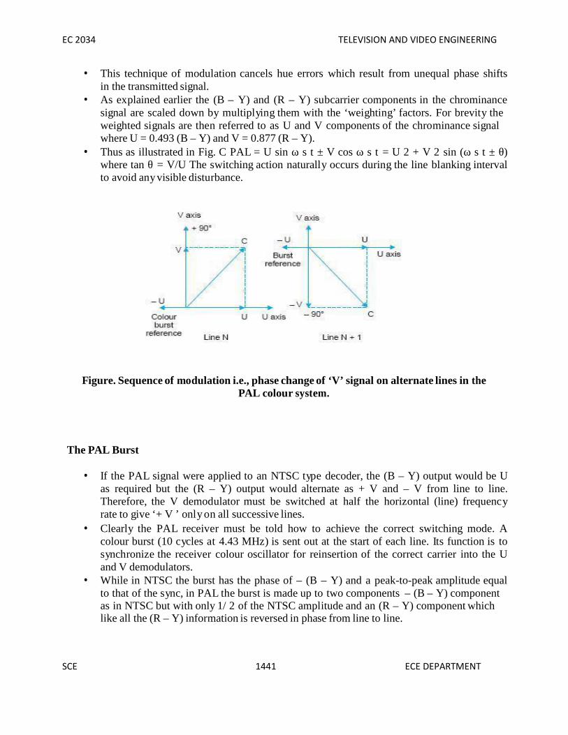
EC 2034 TELEVISION AND VIDEO ENGINEERING
SCE 144144144
ECE DEPARTMENT
This technique of modulation cancels hue errors which result from unequal phase shiftsin the transmitted signal.
As explained earlier the (B – Y) and (R – Y) subcarrier components in the chrominancesignal are scaled down by multiplying them with the ‘weighting’ factors. For brevity theweighted signals are then referred to as U and V components of the chrominance signalwhere U = 0.493 (B – Y) and V = 0.877 (R – Y).
Thus as illustrated in Fig. C PAL = U sin ω s t ± V cos ω s t = U 2 + V 2 sin (ω s t ± θ)where tan θ = V/U The switching action naturally occurs during the line blanking intervalto avoid anyvisible disturbance.
Figure. Sequence of modulation i.e., phase change of ‘V’ signal on alternate lines in thePAL colour system.
The PAL Burst
If the PAL signal were applied to an NTSC type decoder, the (B – Y) output would be Uas required but the (R – Y) output would alternate as + V and – V from line to line.Therefore, the V demodulator must be switched at half the horizontal (line) frequencyrate to give ‘+ V ’ only on all successive lines.
Clearly the PAL receiver must be told how to achieve the correct switching mode. Acolour burst (10 cycles at 4.43 MHz) is sent out at the start of each line. Its function is tosynchronize the receiver colour oscillator for reinsertion of the correct carrier into the Uand V demodulators.
While in NTSC the burst has the phase of – (B – Y) and a peak-to-peak amplitude equalto that of the sync, in PAL the burst is made up to two components – (B – Y) componentas in NTSC but with only 1/ 2 of the NTSC amplitude and an (R – Y) component whichlike all the (R – Y) information is reversed in phase from line to line.

EC 2034 TELEVISION AND VIDEO ENGINEERING
SCE 145145145
ECE DEPARTMENT
This ± (R – Y) burst signal has an amplitude equal to that of the – (B – Y) burst signal, sothat the resultant burst amplitude is the same as in NTSC.
Note that the burst phase actually swings m 45° see about the – (B – Y) axis from line toline. However the sign of (R – Y) burst component indicates the same sign as that of the(R – Y) picture signal.
Thus the necessary switching mode information is always available. Since the colourburst shifts on alternate lines by ± 45° about the zero reference phase it is often called theswinging burst.
Illustration of PAL colour burst swing.
4.4. CANCELLATION OF PHASE ERRORS
As already pointed out the chroma signal is susceptible to phase shift errors both at thetransmitter and in the transmission path.
This effect is sometimes called ‘differential phase error’ and its presence results inchanges of hue in the reproduced picture. This actually results from a phase shift of thecolour sideband frequencies with respect to colour burst phase.
The PAL system has a built-in protection against such errors provided the picture contentremains almost the same from line to line.

EC 2034 TELEVISION AND VIDEO ENGINEERING
SCE 146146146
ECE DEPARTMENT
This is illustrated by phasor diagrams. Figure (a) shows phasors representing particularU and V chroma amplitudes for two consecutive lines of a field. Since there is no phaseerror the resultant phasor (R) has the same amplitude on both the lines.
Detection along the U axis in one synchronous detector and along the V axis in another,accompanied by sign switching in the latter case yields the required U and V coloursignals. Thus correct hues are produced in the picture.
Now suppose that during transmission the phasor R suffers a phase shift by an angle δ.As shown in Fig (b) (i), the corresponding changes in the magnitude of U and V wouldmean a permanent hue error in the NTSC system.
However, in the PAL system ( (b) (ii)) the resultant phasor at the demodulator will swingbetween R 1 and R 2 as illustrated in Fig. (b) (iii). It is now obvious that the phase errorwould cancel out if the two lines are displayed at the same time. In actual practicehowever, the lines are scanned in sequence and not simultaneously.
The colours produced by two successive lines, therefore, will be slightly on either side ofthe actual hue.
Since the lines are scanned at a very fast rate the eye due to persistence of vision willperceive a colour that lies between the two produced by R 1 and R 2 respectively.
Thus the colour seen would more or less be the actual colour. It is here, where the PALsystem claims superiority over the NTSC system.
Figure. No phase error—(i) and (ii) show subcarrier phasors on two consecutive lines while(iii) depicts location of resultant phasor at the demodulator. Note that the phasor (U ± jV)
chosen for this illustration represents a near magenta shade.

EC 2034 TELEVISION AND VIDEO ENGINEERING
SCE 147147147
ECE DEPARTMENT
Figure. Cancellation of phase error.(δ). (i) and (ii) show subcarrier phasors on twoconsecutive lines when a phase shift occurs. (iii) location of resultant phasor at the
demodulator.
4.5. PAL-D COLOUR SYSTEM
The use of eye as the averaging mechanism for the correct hue is the basis of ‘simplePAL’ colour system. However, beyond a certain limit the eye does see the effect ofcolour changes on alternate lines, and so the system needs modification.
Remarkable improvement occurs in the system if a delay line is employed to do theaveraging first and then present the colour to the eye. This is known as PAL-D or DelayLine PAL method and is most commonly used in PAL colour receivers.
As an illustration of the PAL-D averaging technique, Fig shows the basic circuit used forseparating individual U and V products from the chrominance signal. For convenience,both U and V have been assumed to be positive, that is, they correspond to some shade ofmagenta (purple).
Thus for the first line when the V modulator product is at 90° to the + U axis, the phasorcan be expressed as (U + jV). This is called the NTSC line. But on the alternate (next)line when the V phase is switched to – 90°, the phasor becomes (U – jV) and thecorresponding line is then called the PAL line.
As shown in Fig. a delay line and, adding and subtracting circuits are interposed betweenthe chrominance amplifier and demodulators.
The object of the delay line is to delay the chrominance signal by almost exactly one lineperiod of 64 μs. The chrominance amplifier feeds the chrominance signal to the adder,the subtractor and the delay line.

EC 2034 TELEVISION AND VIDEO ENGINEERING
SCE 148148148
ECE DEPARTMENT
Figure. Basic principle of Pal-D demodulation. (b) Summation of consecutive line phasorsin a PAL-D receiver.
The delay line in turn feeds its output to both the adder and subtractor circuits. The adderand subtractor circuits, therefore, receive the two signals simultaneously. These may bereferred to at any given time as the direct line and delay line signals.
For the chosen hue, if the present incoming line is an NTSC line, the signal entering thedelay-line and also reaching the adder and subtractor is (U + jV). But then the previousline must have been the PAL line i.e., (U – jV) and this signal is simultaneously availablefrom the delay line. The result is (see Fig. 26.14 (a)) that the signal information of twopicture lines, though transmitted in sequence, are presented to the adder and subtractorcircuits simultaneously.
The adder yields a signal consisting of U information only but with twice the amplitude(2U). Similarly, the subtraction circuit produces a signal consisting only of Vinformation, with an amplitude twice that of the ‘V ’ modulation product.
To permit precise addition and subtraction of direct and delayed line signals, the delayline must introduce a delay which is equivalent to the duration of an exact number of halfcycles of the chrominance signal.
This requirement would not be met if the line introduced a delay of exactly 64 μs. At afrequency of 4.43361875 MHz the number of cycles which take place in 64 μs are4.43361875 × 10 6 × 64 × 10 –6 = 283.7485998 Hz, ≈ 283.75 Hz.
A delay line which introduces a delay equal to the duration of 283.5 subcarrier cycles istherefore suitable. This is equal to a time delay of 63.943 μs (1/f sc × 283.5). The

EC 2034 TELEVISION AND VIDEO ENGINEERING
SCE 149149149
ECE DEPARTMENT
addition and subtraction of consecutive line phasors can also be illustrated vectorially byphasor diagrams.
Figure is such a phasor diagram pertaining to the phase error illustration of Fig. The Uand V signals thus obtained are fed to their respective synchronous demodulators forrecovery of the colour difference signals Choice of Colour Subcarrier Frequency If thesub-carrier frequency is chosen on the half-line offset basis as is done in the NTSCsystem, an annoying vertical line-up of dots occurs on certain hues. This is due to phasereversal of the sub-carrier at line frequency.
To overcome this difficulty, a quarter-line offset is given instead and f sc is made an oddmultiple of one quarter of the line frequency. For optimum results this is slightlymodified by adding 25 Hz to it, to provide a phase reversal on each successive field.
Thus the actual relationship between f sc , f h and f v can be expressed as
f sc = f h
This on substituting the values of f h and f v gives f sc = 4.43361875 MHz.
It may be mentioned that though formation of any dot pattern on the screen must besuppressed by appropriate choice of sub-carrier frequency, it is of low visibility andappears only when colour transmission is received on a monochrome receiver. Since thechrominance signal disappears on grey or white details in a picture, the interferenceappears only in coloured areas of the scene. All colours appear as shades of grey on amonochrome receiver and thus the dot effect is visible only in those coloured parts of thepicture which are reproduced in lighter shades of grey.
Colour Subcarrier Generation
The colour subcarrier frequency of 4.43361875 MHz is generated with a crystalcontrolled oscillator. In order to accomplish minimum raster disturbance through thecolour subcarrier it is necessary to maintain correct frequency relationships between thescanning frequencies and the subcarrier frequency.
It is therefore usual to count down from the subcarrier frequency to twice the linefrequency (2f h ) pulses which are normally fed to monochrome sync pulse generators.There are several ways in which frequency division can be accomplished. In the earlydays of colour television it was necessary to choose frequencies which had low-orderfactors so that division could take place in easy stages, but such constraints are no longernecessary.
The PAL subcarrier frequency is first generated directly. Then the 25 Hz output obtainedfrom halving the field frequency is subtracted from the subcarrier frequency.
The frequency thus obtained is first divided by 5 and then by 227. Such a large division ispracticable by using a chain of binary counters and feeding back certain of the counteddown pulses to earlier points of the chain that the count down is changed from a divisionof 2 8 to a division of the pal coder
The gamma corrected R, G and B signals are matrixed to form the Y and the weightedcolour difference signals. The bandwidths of both (B – Y) and (R – Y) video signals are

EC 2034 TELEVISION AND VIDEO ENGINEERING
SCE 150150150
ECE DEPARTMENT
restricted to about 1.3 MHz by appropriate low- pass filters. In this process these signalssuffer a small delay relative to the Y signal. In order to compensate for this delay, a delayline is inserted in the path of Y signal.
The weighted colour difference video signals from the filters are fed to correspondingbalanced modulators. The sinusoidal sub-carrier is fed directly to the U modulator butpasses through a ± 90° phase switching circuit on alternate lines before entering the Vmodulator.
Figure. Basic organization of the PAL coder.

EC 2034 TELEVISION AND VIDEO ENGINEERING
SCE 151151151
ECE DEPARTMENT
Since one switching cycle takes two lines, the squarewave switching signal from themultivibrator to the electronic phase switch is of half-line frequency i.e., approximately7.8 KHz.
The double sideband suppressed carrier signals from the modulators are added to yieldthe quadrature amplitude modulated (Q.A.M.) chrominance (C) signal. This passesthrough a filter which removes harmonics of the subcarrier frequency and restricts theupper and lower sidebands to appropriate values.
The output of the filter feeds into an adder circuit where it is combined with theluminance and sync signals to form a composite colour video signal. The bandwidth andlocation of the composite colour signals (U and V) is shown along with the Y signal inFig Notice that the colour burst signal is also fed to the modulators along with the U andV signals through the adders.
The burst signals are obtained from the circuits that feed the colour subcarrier signal tothe two modulators. However, before feeding the burst signals to the U and V addersthese are passed through separate burst gates.
Each burst gate is controlled by delayed pulses at f H rate obtained from the frequencydividing circuit. The gating pulses appear during the back porch period.
Thus, during these intervals the (B – Y) i.e., U modulator yields a subcarrier burst along –U while the (R – Y) i.e., V modulator gives a burst of the same amplitude but having aphase of ± 90° on alternate lines relative to the – U phasor. At the outputs of the twomodulators, the two burst components combine in the adder to yield an output which isthe vector sum of the two burst inputs.
This is a subcarrier sinewave ( ≈ 10 cycles) at + 45° on one line and – 45° on the next linewith reference to – U phasor. The colourplexed composite signal thus formed is fed to themain transmitter to modulate the station channel picture carrier in the normal way.
The sound signal after being frequency modulated with the channel sound carrierfrequency also forms part of the RF signal that is finally radiated through the transmitterantenna system.
4.7. PAL-D COLOUR RECEIVER
Various designs of PAL decoder have been developed. The one shown in the colourreceiver block diagram of Fig. is a commonly used arrangement.
It will be noticed that the general pattern of signal flow is very close to that of the NTSCreceiver. Necessary details of various sections of the receiver are discussed.
1. Tuner
It is necessary to maintain local oscillator frequency at the correct value to obtain exactcolour burst frequency for proper reproduction of different colours in the picture.
Therefore, colour receiver tuners employ an additional circuit known as automaticfrequency tuning (AFT). This circuit actually controls the local oscillator frequency toobtain a picture IF of exactly 38.9 MHz at the converter output.
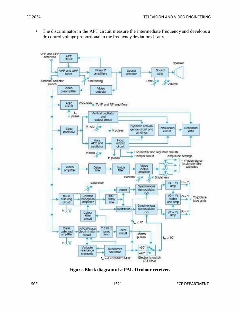
EC 2034 TELEVISION AND VIDEO ENGINEERING
SCE 152152152
ECE DEPARTMENT
The discriminator in the AFT circuit measure the intermediate frequency and develops adc control voltage proportional to the frequency deviations if any.
Figure. Block diagram of a PAL-D colour receiver.

EC 2034 TELEVISION AND VIDEO ENGINEERING
SCE 153153153
ECE DEPARTMENT
This error voltage is applied to the reactance section of the local oscillator to maintain itsfrequency at the correct value. More details of AFT are given in the next chapter alongwith other special circuits.
2. Sound Strip.
The frequency modulated sound IF signal is processed in the usual way to obtain audiooutput. The volume and tone controls are associated with the audio amplifier, the outputof which feeds into the loudspeaker.
Thus the sound strip of a colour receiver is exactly the same as in a black and whitereceiver.
3. AGC, Sync-separator and Deflection Circuits
The AGC and sync-separator circuits function in the same way as in a monochromereceiver. However, the deflection circuits, besides developing normal horizontal and fieldscanning currents also provide necessary wave-forms for dynamic convergence andpincushion correction.
In addition, pulses from the horizontal output transformer are fed to several circuits in thecolour section of the receiver.
4. Luminance Channel
The video amplifier in the luminance channel is dc coupled and has the same bandwidthas in the monochrome receiver. It is followed by a delay line to compensate for theadditional delay the colour signal suffers because of limited bandpass of thechrominance. This ensures time coincidence of the luminance and chrominance signals.The channel also includes a notch filter which attenuates the subcarrier by about 10 db.This helps to suppress the appearance of any dot structure on the screen along with thecolour picture. The inverted composite video signal available at the output of luminancechannel is fed to the junction of three cathodes of the picture tube. This part of the circuitalso includes drive adjustment necessary for setting of the black level and obtainingcorrect reproduction of colours.
5. Colour Signal Processing
The signal available at the output of video detector is given some amplification (videopreamplifier) before feeding it to the various sections. All modern receivers use ICs forprocessing the colour signal. However, for a better understanding, the operation of eachstage is described with the help of discrete component circuitry.
(a) Chrominance bandpass amplifier.
As noted previously the chroma bandpass amplifier selects the chrominance signal andrejects other unwanted components of the composite signal.

EC 2034 TELEVISION AND VIDEO ENGINEERING
SCE 154154154
ECE DEPARTMENT
The burst blanking, colour level control and colour killer switch also form part of thismultistage amplifier. (i) Burst Blanking.
The output from the video preamplifier is fed to the first stage of chroma bandpassamplifier through an emitter follower stage (Q 1 ). Negative going horizontal blankingpulses are coupled to the base of Q 1 through diode D 1 . The pulses drive Q 1 into cut-off during colour burst intervals and thus prevent it from reaching the demodulators. (ii)Bandpass Stage.
The emitter follower output is fed to the bandpass stage through a tuned circuit consistingof L 1 and C 3 . The necessary bandwidth centered around 4.43 MHz is adjusted by R 5and R 6 . The tuning of L 1 also incorporates necessary correction on account of vestigialsideband transmission of the chrominance signal. (iii) Automatic Colour Control (ACC).The biasing of amplifier (Q 2 ) in Fig. 26.17 is determined by the dc control voltage fedto it by the ACC circuit.
The ACC circuit is similar to the AGC circuit used for automatic gain control of RF andIF stages of the receiver. It develops a dc control voltage that is proportional to theamplitude of colour burst. This voltage when fed at the input of Q 2 shifts its operatingpoint to change the stage gain. Thus net overall chroma signal output from the bandpassamplifier tends to remain constant.
iv) Manual Colour (Saturation) Control.
As shown in Fig. the chroma signal from the first stage is applied through R 1 and R 2 tothe emitter of Q 3 and cathode of D 2 , the colour control diode. The diode is forwardbiased by a voltage divider formed by R 3 , R 4 and R 5 the colour control potentiometer.
When the diode is excessively forward biased (R 5 at + 30 V position) it behaves like ashort circuit. Under this condition the chroma signal gets shorted via C 1 to ground andthere is no input to the demodulators. As a result, a black and white picture is producedon the screen. If R 5 is so adjusted that forward bias on D 1 is almost zero, the diodewould present a very high impedance to the signal.
Under this condition all the available signal feeds into the amplifier and a large signalvoltage appears at the output of the chroma bandpass amplifier. This is turn produces apicture with maximum saturation.
At other settings of R 5 , conductance of D 1 would cause the signal current to dividebetween the emitter of Q 3 and C 1 resulting in intermediate levels of picture coloursaturation.
No tint or hue control is provided in PAL receivers because of the inbuilt provision forphase shift cancellation. In same receiver designs the saturation control is combined withthe contrast control.

EC 2034 TELEVISION AND VIDEO ENGINEERING
SCE 155155155
ECE DEPARTMENT
Figure. Saturation control in the chroma bandpass amplifier.
(v) Colour Killer Circuit.
The colour killer and associated circuits are shown in Fig. The forward bias of Q 5 , thelast stage of bandpass amplifier depends on the state of the colour killer circuit.
When a colour signal is being received, the 7.8 KHz (switching rate of the (R – Y) signal)component is available at the APC (automatic phase control) circuit of the referencesubcarrier oscillator. It is applied via C 1 to the base of tuned amplifier Q 6 . Theamplified 7.8 KHz signal is ac coupled to Q 7 .
Diode D 3 conducts on negative half cycles charges the capacitor C 2 with the polaritymarked across it.
The discharge current from this capacitor provides forward bias to Q 7 , the emitterfollower. Such an action results in a square wave signal at the output of Q 7 .
It is coupled back via a 680 ohm resistor to the tuned circuit in the collector of Q 6 . Thisprovides positive feedback and thus improves the quality factor of the tuned circuit.
The colour killer diode D 4 rectifies the square-wave output from the emitter of Q 7 . Theassociated RC filter circuit provides a positive dc voltage at point ‘A’ and this serves asource of forward bias to the chrominance amplifier Q 5 . Diode D 5 is switched on by

EC 2034 TELEVISION AND VIDEO ENGINEERING
SCE 156156156
ECE DEPARTMENT
this bias and so clamps the voltage produced at ‘A’ by the potential divider (3.3 K and680 ohm) across the + 15 V line.
When a monochrome transmission is received there is no 7.8 KHz input to the colourkiller diode D 4 and no positive voltage is developed at its cathode (point A). Both D 5and the base emitter junction of Q 5 are now back biased by the – 20 V potential returnedat ‘A’ via the 220 K resistor.
The chrominance signal channel, therefore, remains interrupted.
Figure. Colour killer and allied circuits.
EC 2034 TELEVISION AND VIDEO ENGINEERING
SCE 157157157
ECE DEPARTMENT
(b) Separation of U and V modulation products.
The addition of two picture lines radiated in sequence but presented to the adder circuitsimultaneously yields a signal consisting of only U information but with an amplitudeequal to twice the amplitude of the chrominance signal’s U modulation product. Similarlythe subtraction of the two lines produces a signal consisting of V information with anamplitude equal to twice that of the V modulation product.
Synchronous Demodulators.
The output from the adder and substractor consists of two independent double sideband,suppressed carrier RF signals. These are the U modulation product and the line-by-linephase inverted V modulation product. The two individual RF signals are fed to theirrespective demodulators.
Each of the demodulators also receives a controlled subcarrier of correct phase to allowrecovery of the colour difference signal waveforms. It may be noted that the modulatorsdo not have to handle Q.A.M. (u ± jv) RF signals as is the case in the NTSC system.
Therefore, it is not absolutely necessary to employ synchronous demodulators. However,synchronous demodulators are preferred in practice because they yield an accurate andconstant no-colour zero voltage level above and below which (sometimes positive andsometimes negative) the colour different signal voltage varies. (c) Colour differenceamplifiers and matrixing.
There are two approaches to driving the colour picture tube. In one scheme, the threecolour difference signals are amplified and fed to the appropriate grids of the picturetube. The – Y signal is fed to the junction of three cathodes for matrixing. In anotherapproach R, G, and B video signals are obtained directly by a suitable matrix from themodulator outputs. Each colour signal is then separately amplified and applied withnegative polarity (– R, – G, – B) to the respective cathodes.
The grids are then returned to suitable negative dc potentials. This, i.e., R, G, B method ispreferred in transistor amplifiers because less drive voltages are necessary when R, G,and B are directly fed to the picture tube.
The use of dc amplifiers would involve difficulties, especially in maintaining a constant‘no colour’ voltage level at the picture tube grids. It is usual to employ ac amplifiers andthen establish a constant no-colour level by employing dc clamps. The clamping isaffected during line blanking periods by pulses derived from the line time base circuitry.
Thus the dc level is set at the beginning of each active line period. The discharge timeconstants of the ac coupling networks are chosen to be quite large so that the dc leveldoes not change significantly between the beginning and end of one active line period.
6. Subcarrier Generation and Control
The primary purpose of this section is to produce a subcarrier of correct frequency toreplace the subcarrier suppressed in the two chrominance signal balanced modulators atthe transmitter end encoder. N

EC 2034 TELEVISION AND VIDEO ENGINEERING
ot only must the generated subcarrier be of exactly the right frequency but it must also beof the same phase reference as the original subcarrier. A crystal oscillator is used in thereceiver and this is forced to work at the correct frequency and phase by the action of anautomatic frequency and phase control circuit.
This is usually called the APC circuit. The APC circuit compares the burst and locallygenerated reference subcarrier to develop a control voltage. The burst signal is obtainedthrough the burst gate amplifier circuit.
The identification circuit and electronic switch for line switching the subcarrier to the Vmodulator also form part of the subcarrier generation circuitry. (a) Burst gate amplifier.The burst gate or burst amplifier as it is often called separates
SCE 158 ECE DEPARTMENT

EC 2034 TELEVISION AND VIDEO ENGINEERING
UNIT 5ADVANCED TELEVISION SYSTEMS
TELEVISION BROADCASTING
Broadcasting means transmission in all directions by electromagnetic waves from thetransmitting station. Broadcasting that deals mostly with entertainment and advertising isprobably the most familiar use of television. Millions of television sets in use around theworld attest to its extreme popularity.
Most programmes produced live in the studio are recorded on video tape at a convenienttime to be shown later. Initially television transmission was confined to the VHF band onlybut later a large number of channel allocations were made in the UHF band also. Thedistance of transmission, as explained earlier, is confined to line of the sight between thetransmitting and receiving antennas.
The useful service range is up to 120 km for VHF stations and about 60 km for UHFstations. Television broadcasting initially started with monochrome picture but around1952 colour transmission was introduced.
Despite its complexity and higher cost, colour television has become such a commercialsuccess that it is fast superseding the monochrome system.
CABLE TELEVISION
In recent year’s master antenna (MATV) and community antenna (CATV) televisionsystems have gained widespread popularity. The purpose of a MATV system is to delivera strong signal (over 1 mV) from one or more antennas to every television receiverconnected to the system.
Typical applications of a MATV system are hotels, motels, schools, apartment buildingsand so on. The CATV system is a cable system which distributes good quality televisionsignal to a very large number of receivers throughout an entire community.
In general, this system feeds increased TV programmes to subscribers who pay a fee forthis service. A CATV system may have many more active (VHF and UHF) channels thana receiver tuner can directly select. This requires use of a special active converter in thehead-end.
(a) MATV
The block diagram of a basic MATV system is shown in Fig. One or more antennas areusually located on roof top, the number depending on a available telecasts and theirdirection.
Each antenna is properly oriented so that all stations are received simultaneously. In orderto allow a convenient match between the coaxial transmission line and components thatmake up the system, MATV systems are designed to have a 75 Ω impedance. Since mostantennas have a 300 Ω impedance, a balun is used to convert the impedance to 75 ohms.
SCE 159 ECE DEPARTMENT

EC 2034 TELEVISION AND VIDEO ENGINEERING
SCE 160160160
ECE DEPARTMENT
As shown in the figure, antenna outputs feed into a 4-way hybrid. A hybrid is basically asignal combining linear mixer which provides suitable impedance matches to preventdevelopment of standing waves.
The standing waves, if present, result in ghosts appearing in an otherwise good TV picture.The output from the hybrid feeds into a distribution amplifier via a preamplifier. Thefunction of these amplifiers is to raise the signal amplitude to a level which is sufficient toovercome the losses of the distribution system while providing an acceptable signal toevery receiver in the system.
The output from the distribution amplifier is fed to splitters through coaxial trunk lines. Asplitter is a resistive-inductive device which provides trunk line isolation and impedancematch. Coaxial distribution lines carry television signals from the output of splitters topoints of delivery called subscriber tap-offs.
The subscriber taps, as shown in Fig, can be either transformer coupled, capacitive coupledor in the form of resistive pads. They provide isolation between receivers on the same linethus preventing mutual interference. The taps look like ac outlets and are normally mountedin the wall.
Wall taps may be obtained with 300 Ω output 75 Ω output and a dual output. The preferredmethod is to use a 75 Ω type with a matching transformer. The matching transformer isusually mounted at the antenna terminals of the receiver and will have a VHF output and aUHF output.
Since improperly terminated lines will develop standing waves, the end of each 75 Ωdistribution cable is terminated with a 75 Ω resistor called a terminator.
(b) CATV
Formerly CATV system were employed only in far-fringe areas or in valleys surroundedby mountains where reception was difficult or impossible because of low level signalconditions.
However, CATV systems are now being used in big cities where signal-level is high butall buildings render signals weak and cause ghosts due to multipath reflections. In eithercase, such a system often serves an entire town or city.
A single antenna site, which may be on top of a hill, mountain or sky-scraper is chosen forfixing antennas. Several high gain and properly oriented antennas are employed to pick upsignals from different stations. In areas where several signals are coming from onedirection, a single broad based antenna (log-periodic) may be used to cover those channels.
Most cable television installations provide additional services like household, business andeducational besides commercial TV and FM broadcast programmes. These include news,local sports and community programmes, burglar and fire alarms, weather reports,commercial data retrieval, meter reading, document reproduction etc.
Educational services include computer aided instructions, centralized library services andso on. Many of the above options require extra subscription fee from the subscriber.

EC 2034 TELEVISION AND VIDEO ENGINEERING
SCE 161161161
ECE DEPARTMENT
Figure. The modern cable TV system
Since several of the above mentioned service need two-way communication between thesubscriber and a central processor, the coaxial distribution network has a large number ofcable pairs, usually 12 or 24.
This enables the viewer to choose any channel or programme out of the many that areavailable at a given time. CATV Plan. Figure 10.2 shows the plan of a typical CATVsystem. The signals from various TV channels are processed in the same manner as in aMATV system. In fact, a CATV system can be combined with a MATV set-up.
When UHF reception is provided in addition to VHF, as often is the case, the signal fromeach UHF channel is processed by a translator. A translator is a frequency converter whichhterodynes the UHF channel frequencies down to a VHF channel.
Translation is advantageous since a CATV system necessarily operates with lengthycoaxial cables and the transmission loss through the cable is much greater at UHF than atVHF frequencies. As in the case of MATV, various inputs including those from translatorsare combined in a suitable mixer.
The set-up from the antennas to this combiner is called a head-end. Further, as shown inthe figure the CATV outputs from the combiner network are fed to a number of trunk cables

EC 2034 TELEVISION AND VIDEO ENGINEERING
SCE 162162162
ECE DEPARTMENT
through a broadband distribution amplifier. The trunk cables carry signals from the antennasite to the utilization site (s) which may be several kilometers away. Feeder amplifiers areprovided at several points along the line to overcome progressive signal attenuation whichoccurs due to cable losses.
Since cable losses are greater at higher frequencies it is evident that high-band attenuationwill be greater than low-band attenuation. Therefore, to equalize this the amplifiers andsignal splitters are often supplemented by equalizers. An equalizer or tilt control consistsof a band pass filter arrangement with an adjustable frequency response. It operates byintroducing a relative low-frequency loss so that outputs from the amplifiers or splittershave uniform relative amplitude response across the entire VHF band.
The signal distribution from splitters to tap-off points is done through multicore coaxialcables in the same way as in a MATV system. In any case the signal level provided to atelevision receiver is of the order of 1.5 mV.
This level provides good quality reception without causing accompanying radiationproblems from the CATV system, which could cause interference to other installations andservices.
Signal Processing
The TV signals to be redistributed by the cable company usually undergo some kind ofprocessing before they are put on the cable to the TV set. Amplification and impedancematching are the main processes involved in sending the signal to remote locations overwhat is sometimes many miles of coaxial cable. However, at the head end, other types ofprocesses are involved.(Coaxial or fiber-optic cable)Frequency synthesized local oscillator
Straight-Through Processors.
In early cable systems, the TV signals from local stations were picked up with antennas,and the signal was amplified before being multiplexed onto the main cable. This is calledstraight-through processing. Amplifiers called strip amplifiers and tuned to the receivedchannels pass the desired TV signal to the combiner.
Most of these amplifiers include some kind of gain control or attenuators that can reducethe signal level to prevent distortion of strong local signals. This process can still be usedwith local VHF TV stations, but today heterodyne processing is used instead.
Heterodyne Processors.
Heterodyne processing translates the incoming TV signal to a different frequency. This isnecessary when satellite signals are involved.
Microwave carriers cannot be put on the cable, so they are down-converted to someavailable 6-MHz TV channel.

EC 2034 TELEVISION AND VIDEO ENGINEERING
SCE 163163163
ECE DEPARTMENT
In addition, heterodyne processing gives the cable companies the flexibility of putting thesignals on any channel they want to use.
The cable TV industry has created a special set of non-broadcast TV channels, some of thefrequency assignments correspond to standard TV channels, but others do not. Since allthese frequencies are confined to a cable, there can be duplication of any frequency thatmight be used in radio or TV broadcasting.
Note that the spacing between the channels is 6 MHz.
Satellite TV
One of the most common methods of TV signal distribution is via communicationsatellite.A communication satellite orbits the equator about 22,300 mi out in space. Itrotates in synchronism with the earth and therefore appears to be stationary. Thesatellite is used as a radio relay station.
The TV signal to be distributed is used to modulate a microwave carrier, and then it istransmitted to the satellite. The path from earth to the satellite is called the uplink. Thesatellite translates the signal to another frequency and then retransmits it back to earth.This is called the downlink. A receive site on earth picks up the signal.
The receive site may be a cable TV company or an individual consumer. Satellites arewidely used by the TV networks, the premium channel companies, and the cable TVindustry for distributing signals nationally.
A newer form of consumer satellite TV is direct broadcast satellite (DBS) TV. TheDBS systems are designed specifically for consumer reception directly from thesatellite. The new DBS systems feature digitally encoded video and audio signals,which make transmission and reception more reliable and provide outstanding pictureand sound quality.
By using higher-frequency microwaves, higher-power satellite transponders, and verylow-noise GaAs FETs in the receiver, the customer’s satellite dish can be made verysmall. These systems typically use an 18-in dish as opposed to the 5- to 12-ft-diameterdishes still used in older satellite TV systems.
Direct Broadcast Satellite Systems The direct broadcast satellite (DBS ) system was designed specifically to be an all-
digital system. Data compression techniques are used to reduce the data rate requiredto produce high-quality picture and sound.
The DBS system features entirely digital uplink ground stations and satellites. Sincethe satellites are designed to transmit directly to the home, extra high-powertransponders are used to ensure a satisfactory signal level.
To receive the digital video from the satellite, a consumer must purchase a satelliteTV receiver and antenna.

EC 2034 TELEVISION AND VIDEO ENGINEERING
SCE 164164164
ECE DEPARTMENT
These satellite receivers operate in the band. By using higher frequencies as well as higher-power satellite transponders, the necessary dish antenna can be extremely small. The newsatellite DBS system antennas have only an 18-in diameter.
Several special digital broadcast satellites are in orbit, and two of the direct satellite TVsources are DirecTV and DISH Network. They provide full coverage of the major cablenetworks, and the premium channels usually distributed to homes by cable TV and can bereceived directly.
In addition to purchasing the receiver and antenna, the consumer must subscribe to one ofthe services supplying the desired channels. Satellite Transmission. The video to betransmitted must first be placed into digital form. To digitize an analog signal, it must besampled a minimum of 2 times per cycle for sufficient digital data to be developed forreconstruction of the signal.
Assuming that video frequencies of up to 4.2 Mbps are used, the minimum sampling rateis twice this, or 8.4 Mbps. For each sample, a binary number proportional to the lightamplitude is developed. This is done by an A/D converter, usually with an 8-bit output.The resulting video signal, therefore, has a data rate of 8 bits, 8.4 Mbps, or 67.2 Mbps. Thisis an extremely high data rate.
However, for a color TV signal to be transmitted in this way, there must be a separate signalfor each of the red, green, and blue components making up the video. This translates to atotal data rate of or 202, Mbps. Even with today’s technology, this is an extremely highdata rate that is hard to achieve reliably.
To lower the data rate and improve the reliability of transmission, the new DBS systemuses compressed digital video. Once the video signals have been put into digital form, theyare processed by digital signal processing (DSP) circuits to minimize the full amount ofdata to be transmitted.
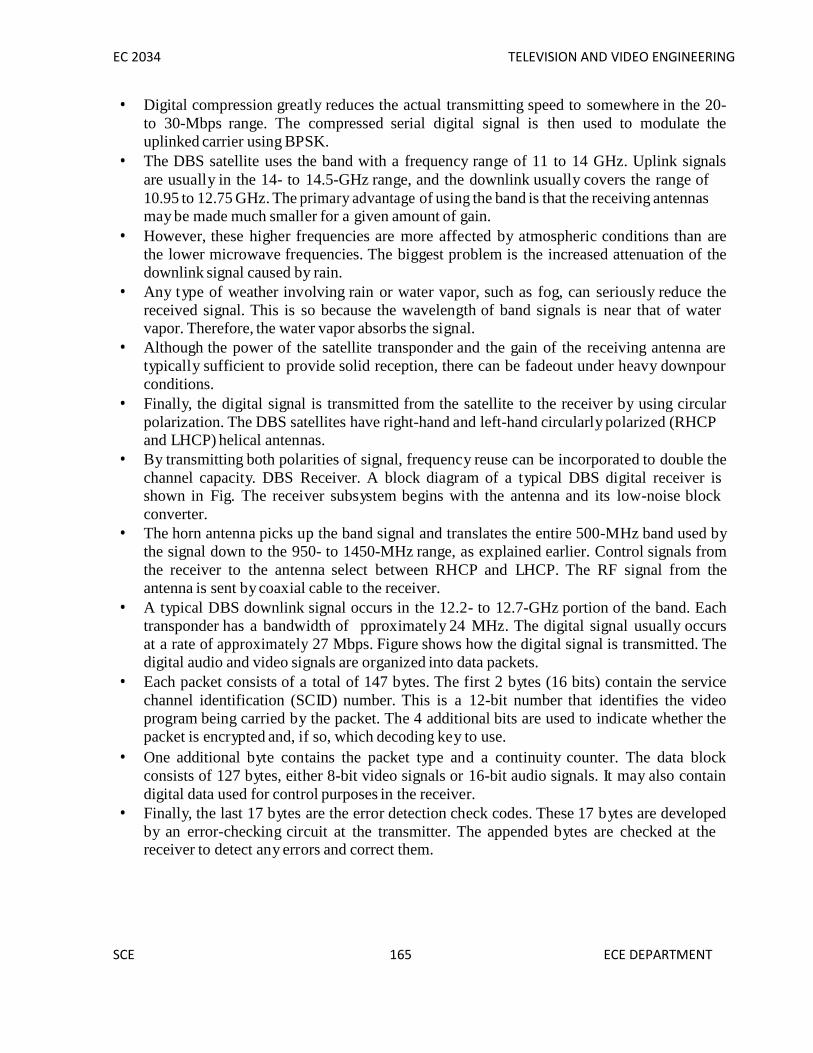
EC 2034 TELEVISION AND VIDEO ENGINEERING
SCE 165165165
ECE DEPARTMENT
Digital compression greatly reduces the actual transmitting speed to somewhere in the 20-to 30-Mbps range. The compressed serial digital signal is then used to modulate theuplinked carrier using BPSK.
The DBS satellite uses the band with a frequency range of 11 to 14 GHz. Uplink signalsare usually in the 14- to 14.5-GHz range, and the downlink usually covers the range of10.95 to 12.75 GHz. The primary advantage of using the band is that the receiving antennasmay be made much smaller for a given amount of gain.
However, these higher frequencies are more affected by atmospheric conditions than arethe lower microwave frequencies. The biggest problem is the increased attenuation of thedownlink signal caused by rain.
Any type of weather involving rain or water vapor, such as fog, can seriously reduce thereceived signal. This is so because the wavelength of band signals is near that of watervapor. Therefore, the water vapor absorbs the signal.
Although the power of the satellite transponder and the gain of the receiving antenna aretypically sufficient to provide solid reception, there can be fadeout under heavy downpourconditions.
Finally, the digital signal is transmitted from the satellite to the receiver by using circularpolarization. The DBS satellites have right-hand and left-hand circularly polarized (RHCPand LHCP) helical antennas.
By transmitting both polarities of signal, frequency reuse can be incorporated to double thechannel capacity. DBS Receiver. A block diagram of a typical DBS digital receiver isshown in Fig. The receiver subsystem begins with the antenna and its low-noise blockconverter.
The horn antenna picks up the band signal and translates the entire 500-MHz band used bythe signal down to the 950- to 1450-MHz range, as explained earlier. Control signals fromthe receiver to the antenna select between RHCP and LHCP. The RF signal from theantenna is sent by coaxial cable to the receiver.
A typical DBS downlink signal occurs in the 12.2- to 12.7-GHz portion of the band. Eachtransponder has a bandwidth of pproximately 24 MHz. The digital signal usually occursat a rate of approximately 27 Mbps. Figure shows how the digital signal is transmitted. Thedigital audio and video signals are organized into data packets.
Each packet consists of a total of 147 bytes. The first 2 bytes (16 bits) contain the servicechannel identification (SCID) number. This is a 12-bit number that identifies the videoprogram being carried by the packet. The 4 additional bits are used to indicate whether thepacket is encrypted and, if so, which decoding key to use.
One additional byte contains the packet type and a continuity counter. The data blockconsists of 127 bytes, either 8-bit video signals or 16-bit audio signals. It may also containdigital data used for control purposes in the receiver.
Finally, the last 17 bytes are the error detection check codes. These 17 bytes are developedby an error-checking circuit at the transmitter. The appended bytes are checked at thereceiver to detect any errors and correct them.
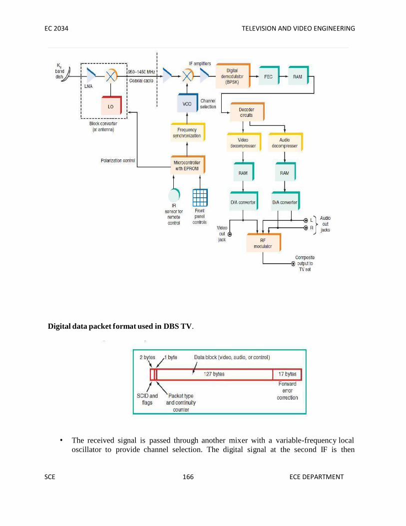
EC 2034 TELEVISION AND VIDEO ENGINEERING
SCE 166166166
ECE DEPARTMENT
Digital data packet format used in DBS TV.
The received signal is passed through another mixer with a variable-frequency localoscillator to provide channel selection. The digital signal at the second IF is then

EC 2034 TELEVISION AND VIDEO ENGINEERING
SCE 167167167
ECE DEPARTMENT
demodulated to recover the originally transmitted digital signal, which is passed through aforward error correction (FEC) circuit.
This circuit is designed to detect bit errors in the transmission and to correct them on thefly. Any bits lost or obscured by noise during the transmission process are usually caughtand corrected to ensure a near-perfect digital signal.
The resulting error-corrected signals are then sent to the audio and video decompressioncircuits. Then they are stored in random access memory (RAM), after which the signal isdecoded to separate it into both the video and the audio portions.
The DBS TV system uses digital compression-decompression standards referred to asMPEG2 (MPEG means Moving Picture Experts Group, which is a standards organizationthat establishes technical standards for movies and video).
MPEG2 is a compression method for video that achieves a compression of about 50 to 1in data rate. Finally, the signals are sent to D/A converters that modulate the RF modulatorwhich sends the signals to the TV set antenna terminals.
Although the new DBS digital systems will not replace cable TV, they provide theconsumer with the capability of receiving a wide range of TV channels. The use of digitaltechniques provides an unusually high-quality signal.
Digital TV (DTV)
Digital TV (DTV), also known as high-definition TV (HDTV), was designed to replacethe National Television Standards Committee (NTSC) system, which was invented in the1940s and 1950s.
The goal of HDTV is to greatly improve the picture and sound quality. After more than adecade of evaluating alternative HDTV systems, the FCC has finalized the standards anddecreed that HDTV will eventually become the U.S. TV standard by April 2009.
The first HDTV stations began transmission in the 10 largest U.S. cities on September 1,1998. HDTV sets can now be purchased by the consumer, but they are still expensive. Asmore HDTV stations come online and as more HDTV programming becomes available,more consumers will buy HDTV receivers and the cost will drop dramatically.
The HDTV system is an extremely complex collection of digital, communication andcomputer techniques.
A full discussion is beyond the scope of this book. However, this section is a briefintroduction to the basic concepts and techniques used in HDTV. HDTV Standards HDTVfor the United States was developed by the Advanced Television Systems Committee(ATSC) in the 1980s and 1990s.
HDTV uses the scanning concept to paint a picture on the CRT, so you can continue tothink of the HDTV screen in terms of scan lines, as you would think of the standard NTSCanalog screen. However, you should also view the HDTV screen as being made up ofthousands of tiny dots of light, called pixels.
Each pixel can be any of 256 colors. These pixels can be used to create any image. Thegreater the number of pixels on the screen, the greater the resolution and the finer the detailthat can be represented.

EC 2034 TELEVISION AND VIDEO ENGINEERING
SCE 168168168
ECE DEPARTMENT
Each horizontal scan line is divided into hundreds of pixels. The format of a HDTV screenis described in terms of the numbers of pixels per horizontal line by the number of verticalpixels (which is the same as the number of horizontal scan lines).
One major difference between conventional NTSC analog TV and HDTV is that HDTVcan use progressive line scanning rather than interlaced scanning. In progressive scanningeach line is scanned one at a time from top to bottom.
Since this format is compatible with computer video monitors, it is possible to displayHDTV on computer screens. Interlaced scanning can be used on one of the HDTV formats.Interlaced scanning minimizes flicker but complicates the video compression process.Progressive scanning is preferred and at a 60-Hz frame rate, flicker is not a problem.
The FCC has defined a total of 18 different formats for HDTV. Most are variations of thebasic formats as given in Table. Most plasma, LCD and larger screens only display theseformats.The 480p (the p stands for “progressive”) standard offers performance comparableto that of the NTSC system. It uses a 4:3 aspect ratio for the screen.
The scanning is progressive. The vertical scan rate is selectable to fit the type of videobeing transmitted. This format is fully compatible with modern VGA computer monitors.
The format can use either progressive or interlaced scanning with either aspect ratio at thethree vertical scan rates shown in Table.
The 720p format uses a larger aspect ratio of 16:9 (a 4:3 format is optional at this resolutionalso). This format is better for showing movies. Figure shows the difference between thecurrent and new HDTV aspect ratios.
The 1080i format uses the 16:9 aspect ratio but with more scan lines and more pixels perline. This format obviously gives the best resolution. The HDTV set should be able todetect and receive any available format. The 720p at 60 Hz and 1080i formats are thosedesignated HDTV.
HDTV Transmission Concepts
In HDTV both the video and the audio signals must be digitized by A/D converters andtransmitted serially to the receiver.

EC 2034 TELEVISION AND VIDEO ENGINEERING
SCE 169169169
ECE DEPARTMENT
Because of the very high frequency of video signals, special techniques must be used totransmit the video signal over a standard 6-MHz-bandwidth TV channel.
And because both video and audio must be transmitted over the same channel, multiplexingtechniques must be used. The FCC’s requirement is that all this information be transmittedreliably over the standard 6-MHz TV channels now defined for NTSC TV. Assume thatthe video to be transmitted contains frequencies up to 4.2 MHz.
For this signal to be digitized, it must be sampled at least 2 times per cycle or at a minimumsampling rate of 8.4 MHz. If each sample is translated to an 8-bit word (byte) and the bytesare transmitted serially, the data stream has a rate of , or 67.2 MHz.
Multiply this by 3 to get 67.2 _ 3 = 201.6 MHz. Add to this the audio channels, and thetotal required bandwidth is almost 300 MHz. To permit this quantity of data to betransmitted over the 6-MHz channel, special encoding and modulation techniques are used.
HDTV Transmitter

EC 2034 TELEVISION AND VIDEO ENGINEERING
SCE 170170170
ECE DEPARTMENT
Figure shows a block diagram of an HDTV transmitter. The video from the camera consistsof the R, G, and B signals that are converted to the luminance and chrominance signals.These are digitized by A/D converters. The luminance sampling rate is 14.3 MHz, and thechroma sampling rate is 7.15 MHz.
The resulting signals are serialized and sent to a data compressor. The purpose of thisdevice is to reduce the number of bits needed to represent the video data and thereforepermit higher transmission rates in a limited-bandwidth channel. MPEG-2 is the datacompression method used in HDTV.
The MPEG-2 data compressor processes the data according to an algorithm that effectivelyreduces any redundancy in the video signal. For example, if the picture is one-half lightblue sky, the pixel values will be the same for many lines.
All this data can be reduced to one pixel value transmitted for a known number of times.The algorithm also uses fewer bits to encode the color than to encode the brightnessbecause the human eye is much more sensitive to brightness than to color.
The MPEG-2 encoder captures and compares successive frames of video and comparesthem to detect the redundancy so that only differences between successive frames aretransmitted. The signal is next sent to a data randomizer. The randomizer scrambles orrandomizes the signal.
This is done to ensure that random data is transmitted even when no video is present orwhen the video is a constant value for many scan lines. This permits clock recovery at thereceiver.
Next the random serial signal is passed through a Reed-Solomon (RS) error detection andcorrection circuit. This circuit adds extra bits to the data stream so that transmission errors

EC 2034 TELEVISION AND VIDEO ENGINEERING
SCE 171171171
ECE DEPARTMENT
can be detected at the receiver and corrected. This ensures high reliability in signaltransmission even under severe noise conditions.
In HDTV, the RS encoder adds 20 parity bytes per block of data that can provide correctionfor up to 10 byte errors per block. The signal is next fed to a trellis encoder. This circuitfurther modifies the data to permit error correction at the receiver. Trellis encoding iswidely used in modems.
Trellis coding is not used in the cable TV version of HDTV. The audio portion of theHDTV signal is also digital. It provides for compact disk (CD) quality audio. The audiosystem can accommodate up to six audio channels, permitting monophonic sound, stereo,and multichannel surround sound.
The channel arrangement is flexible to permit different systems. For example, one channelcould be used for a second language transmission or closed captioning. Each audio channelis sampled at a 48-kbps rate, ensuring that audio signals up to about 24 kHz are accuratelycaptured and transmitted.
Each audio sample is converted to an 18-bit digital word. The audio information is time-multiplexed and transmitted as a serial bit stream at a frequency of A data compressiontechnique designated AC-3 is used to speed up audio transmission.
Next the video and audio data streams are packetized; i.e., they are converted to shortblocks of data bytes that segment the video and audio signals.
These packets are multiplexed along with some synchronizing signals to form the finalsignal to be transmitted. The result is a 188-bit packet containing both video and audio dataplus 4 bytes of synchronizing bytes and a header. See Fig.
The header identifies the number of the packet and its sequence as well as the video format.Next the packets are assembled into frames of data representing one frame of video. Thecomplete frame consists of 626 packets transmitted sequentially. The final signal is sent tothe modulator.
The modulation scheme used in HDTV is 8-VSB, or eight-level vestigial sideband,amplitude modulation. The carrier is suppressed, and only the upper sideband istransmitted.
The serial digital data is sent to a D/A converter where each sequential 3-bit group isconverted to a discrete voltage level. This system encodes 3 bits per symbol, therebygreatly increasing the data rate within the channel. An example is shown in Fig. Each 3-bitgroup is converted to a relative level of or This is the signal that amplitude-modulates thecarrier.
he resulting symbol rate is 10,800 symbols per second. This translates to a data rate of .Eliminating the extra RS and trellis bits gives an actual video/audio rate of about 19.3Mbps. A modified version of this format is used when the HDTV signal is to be transmittedover a cable system. Trellis coding is eliminated and 16-VSB modulation is used to encode4 bits per symbol.
This gives double the data rate of terrestrial HDTV transmission (38.6 Mbps). The VSBsignal can be created with a balanced modulator to eliminate the carrier and to generate thesidebands.
One sideband is removed by a filter or by using the phasing system. The modulated signalis up-converted by a mixer to the final transmission frequency, which is one of the standard
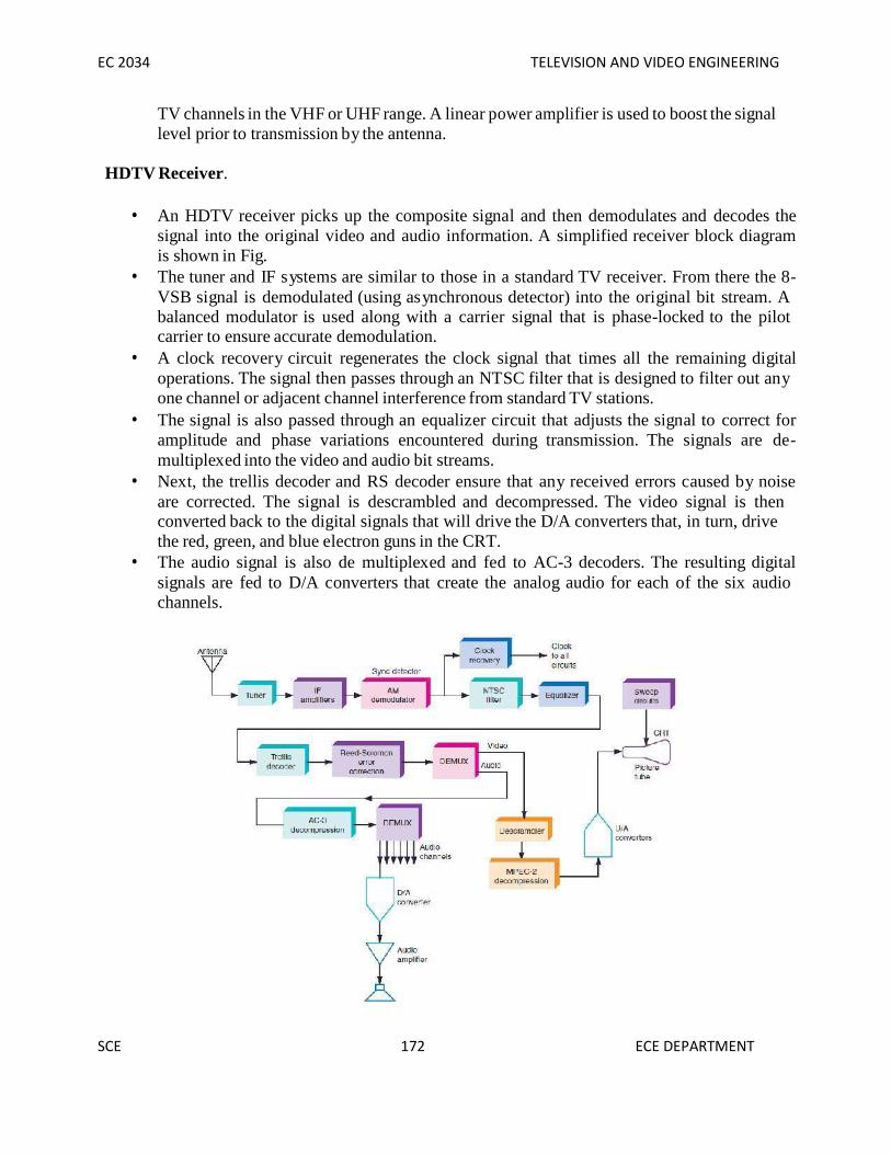
EC 2034 TELEVISION AND VIDEO ENGINEERING
SCE 172172172
ECE DEPARTMENT
TV channels in the VHF or UHF range. A linear power amplifier is used to boost the signallevel prior to transmission by the antenna.
HDTV Receiver.
An HDTV receiver picks up the composite signal and then demodulates and decodes thesignal into the original video and audio information. A simplified receiver block diagramis shown in Fig.
The tuner and IF systems are similar to those in a standard TV receiver. From there the 8-VSB signal is demodulated (using asynchronous detector) into the original bit stream. Abalanced modulator is used along with a carrier signal that is phase-locked to the pilotcarrier to ensure accurate demodulation.
A clock recovery circuit regenerates the clock signal that times all the remaining digitaloperations. The signal then passes through an NTSC filter that is designed to filter out anyone channel or adjacent channel interference from standard TV stations.
The signal is also passed through an equalizer circuit that adjusts the signal to correct foramplitude and phase variations encountered during transmission. The signals are de-multiplexed into the video and audio bit streams.
Next, the trellis decoder and RS decoder ensure that any received errors caused by noiseare corrected. The signal is descrambled and decompressed. The video signal is thenconverted back to the digital signals that will drive the D/A converters that, in turn, drivethe red, green, and blue electron guns in the CRT.
The audio signal is also de multiplexed and fed to AC-3 decoders. The resulting digitalsignals are fed to D/A converters that create the analog audio for each of the six audiochannels.

EC 2034 TELEVISION AND VIDEO ENGINEERING
SCE 173173173
ECE DEPARTMENT
SCRAMBLING AND CONDITIONAL ACCESS SYSTEMS:
Scrambling: It is to suppress the sync signals at transmitting end The picture without Hand V sync cannot lock into steady picture seen as rolling picture and diamond bars. Fordescrambling, a pilot carrier containing the sync timing information is transmitted onseparate carrier.
Another method with great security and complexity is baseband scrambling, the scrambledcoded lines are decoded and it requires demodulation process.
Scrambling is possible by digital processing of video and audio and introducing complexencryption and smart keyboard for controlled access.
Now Addressable converters: includes tunable converters and address recognizationcircuitry which is controlled by computer so specific channels are turned OFF or ON tosubscriber.
CONDITIONAL ACCESS
Features: Equipment compatibity access, support, user system interface, telephone communication
module. The techniques used are scramblers and injectors upstream and descramblermodules.In cable and satellite systems, 3 different operational are projected1. Access to a given channel for fixed duration2. Pay per view with preselected choice of channel3. Pay per view without preselction.
TELETEXT O F VIDEO TEXT SYSTEM
Videotext is a two-way information service as video display unit or crt terminal.Thisinformation service generally provides data in 4 major areas,
1. Finance stock exchanges2. Money markets and reservation3. Messaging- topical news and reviews a subscriber to database can select desired
information via keypad accessory.4. Prestel - first video text service.

EC 2034 TELEVISION AND VIDEO ENGINEERING
SCE 174174174
ECE DEPARTMENT
View data systems use all kinds of host computers, from minicomputers to mainframesdepends upon power require for service.
View data chip (lucy)
It performs most of hardware functions of a viewdata terminal- autodialer circuit, banddemodulator and asynchronous receiver, baud modulator and asynchronous transmitter. It includesa tape interface for recording and character codes. View data terminals CRT displays are used todisplay the information for viewing and editing. It can be an intelligent terminal ormicrocomputers. Intelligent terminals- equipped with microprocessor and data storage memorycapacity to process the data. Microcomputers – with software for data storage and local processingcapability. TV monitor is enhanced with video bandwidth to improve resolution as CRT displaymonitor or VDU.
DIGITAL TV SYSTEM Analog signals suffers degradation due to noise, crosstalk, linear and non-linear distortion.
In this, analog is converted to digital by analog to digital converter ADC performs sampling,quantization and encoding.Sampling:
The TV signal is sampled at rate of twice the maximum band limit frequency- Nyquistcriteria.
Fourier transform of band limit signal at T seconds is scaled by 1/T and given by wo =2π/T.
If input signal is not band limited or sampling frequency does not meet the requirement ofsampling theorem, the various components of spectrum overlap.
It suffers from distortion called aliasing effect and moiré patterns appear in picture.

EC 2034 TELEVISION AND VIDEO ENGINEERING
SCE 175175175
ECE DEPARTMENT
To avoid aliasing errors, the sampling frequency must exceed 10mhz.Quantization:
The sampled output, discrete in time in continuous in amplitude and assigned a discretenumerical values as ADC.
Since DAC is reverse process.Encoder:
The sampled value is assign a binary code along with additional coding like parity for errordetection , scrambling,etc.
Errors occurred are eliminated by redundancy in digital signals. Because of this, delay may occurs in TV , so forward error correction (FEC) is obtained. Block coding and convolution coding are two approaches in this direction.
3DTV
For 3D picture, we have to show the depth also along with length and breadth.( L + B + H)
Principle:
The left and right eye of human see a different image of same object, so brain interpretsthese as a single composite image in 3D.
Two different images are generated by 2 cameras, like our eyes located. For stereo sound transmitter, the left and right channel signals are FM at 5.5MHz audio
carrier. The combined audio and video signals are amplitude modulated by channel carrier using
separate modulators. USB and LSB selected and combined before final transmission.
3-D Display methods:
By using 3 set of color signals we reproduce the 3-D effect on picture tube screen.
First method:
All green color phosphor strips excited by green(G) video signal right. Similarly red colorphosphor strips excited by red(R) video signal left.
Blue (B) color phosphor strips are not exited at all. If viewer wears, G filter at right eye and R filter at left eye, than brain combined to form
various Y shades.

EC 2034 TELEVISION AND VIDEO ENGINEERING
SCE 176176176
ECE DEPARTMENT
Second method:
Two video display units(VDU) are used, to create 3D pictures in natural colors. A polarizing film is fitted in front of VDU and light outputs are reflected using a mirror
arrangement on screen.
Third method:
This is known as ABDY 3D system. In this, R color information are delayed by nearly 600ns and it is obtain by using delay
circuits. So, double image is formed on screen of picture tube.
VCR- VIDEO CASSETTE RECORDERINTRODUCTION
The main purpose of the video recorder is recording and replaying video and audio signals.Although built-in tuners and timers have become integral parts of the average videorecorder, they are not prerequisites for reaching the main goal: audio and video registrationand playback.
THE HELICAL SCAN SYSTEM
In an audio cassette deck, which only registers audio signals, the tape passes over a staticrecording/playback head at constant speed.
The higher the speed of the tape, the more tape particles pass the head opening and thehigher the frequencies that can be registered. Thanks to the extremely narrow head opening,it is possible to record and play back the entire tone range, up to 18,000 or 20,000 Hz,despite a slow tape speed of no more than 4.75 centimeters per second.
However, to register video signals, a range of 3.2 MHz is required and so a tape speed ofapproximately 5 meters per second is a prerequisite. This is over 100 times as fast as thetape speed for an audio cassette deck.
The required high recording speed for video recorders is realized by the helical scan systemwithout such high tape speeds. The system basically consists of a revolving head drum,that has a minimum of two video heads.
The head drum has a diameter of approximately 5 cm and rotates at a speed of 1500revolutions per minute. The 1/2" (12.65 mm) wide videotape is guided around half thesurface of this drum, in a slightly oblique manner. This is achieved by positioning the headdrum at a slight angle.
The tape guidance mechanism then ensures that the tape is guided through the device at aspeed of approximately 2 cm per second (half of the low tape speed that is used in audiocassette decks).

EC 2034 TELEVISION AND VIDEO ENGINEERING
SCE 177177177
ECE DEPARTMENT
Fig:Tape guidance along the head drum with the video heads writing tracks on the tape.
In the meantime, the rapidly revolving video heads write narrow tape tracks of no morethan 0.020 to 0.050 mm wide on the tape, next to each other, diagonally. Every halfrevolution, each of the two heads writes one diagonal track which equals half an image.The first head writes one track, i.e., the first field (the odd numbered scanning lines).
The second head writes a second track, i.e., the other half of the image (the second field:the even numbered scanning lines), which precisely fits in the first image. This correspondsto the interlacing principle, as applied in television.
One full revolution of both heads results in two diagonal tracks right next to each other,together forming one entire image scan (a frame). This means that two apparentlycontradictory requirements can be realized simultaneously: low tape speed of only 2 cmper second and at the same time a high registration speed (relative tape speed) of no lessthan 5 meters per second.
These two requirements make it possible to record the high video frequencies up to 3.2MHz. At the same time, the low tape speed gives a time capacity up to three hours.
SYNCHRONIZATION TRACK
The revolutionary speed of the head drum and the video heads needs to maintain aconstancy within strict parameters. Moreover, the tracks must be scanned during playbackin precisely the same way as they were recorded.
Each tape track is synchronized at the recording stage by means of field synchronizationpulses. These pulses are generated in the video recorder by a separate head which arerecorded on a separate narrow track at the side of the video tape.
This is called the synchronization, servo or control track.

EC 2034 TELEVISION AND VIDEO ENGINEERING
SCE 178178178
ECE DEPARTMENT
Fig: Position of the video, audio and synchronization tracks on the tape.
Fig: Position of the audio, sync and erase heads inside the VCR.
VIDEO DISC SYSTEMS
There are three major video systems in use today:1. Video Home System (VHS)2. Betamax3. Video Hi8
When the video recorders were first introduced, Philips also developed a system calledV2000. Despite the fact that is was a high quality system, it was not successful in themarket.
Although Betamax was reasonably successful at first, its popularity waned and VHS wasadopted as the world standard.

EC 2034 TELEVISION AND VIDEO ENGINEERING
SCE 179179179
ECE DEPARTMENT
BETAMAX
The Sony Betamax System, launched in 1975, was based on the pre-existing professionalSony U-matic-system. In the Betamax system, the video tape is guided along the head drumin a U-shape for all tape guidance functions, such as recording, playback and fastforward/backward.
When the cassette is inserted, the tape is guided around the head drum (called threading).Threading the tape takes a few seconds, but once the tape is threaded, shifting from onetape function to another can be achieved rapidly and smoothly.
Fig:The Betamax U-system before (top) and after (bottom) threading.
VIDEO HOME SYSTEM (VHS)
JVC's VHS System was introduced one year after the launch of Betamax. In VHS, the tapeis guided through in an M-shape; the so-called M-tape guidance system.
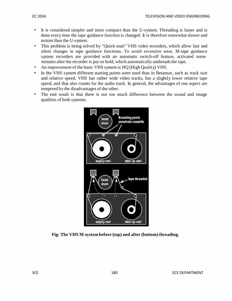
EC 2034 TELEVISION AND VIDEO ENGINEERING
It is considered simpler and more compact than the U-system. Threading is faster and isdone every time the tape guidance function is changed. It is therefore somewhat slower andnoisier than the U-system.
This problem is being solved by "Quick-start" VHS video recorders, which allow fast andsilent changes in tape guidance functions. To avoid excessive wear, M-tape guidancesystem recorders are provided with an automatic switch-off feature, activated someminutes after the recorder is put on hold, which automatically unthreads the tape.
An improvement of the basic VHS system is HQ (High Quality) VHS. In the VHS system different starting points were used than in Betamax, such as track size
and relative speed. VHS has rather wide video tracks, but a slightly lower relative tapespeed, and that also counts for the audio track. In general, the advantages of one aspect aretempered by the disadvantages of the other.
The end result is that there is not too much difference between the sound and imagequalities of both systems.
Fig: The VHS M-system before (top) and after (bottom) threading.
SCE 180 ECE DEPARTMENT
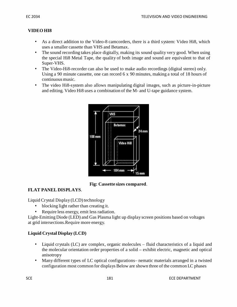
EC 2034 TELEVISION AND VIDEO ENGINEERING
VIDEO HI8
As a direct addition to the Video-8 camcorders, there is a third system: Video Hi8, whichuses a smaller cassette than VHS and Betamax.
The sound recording takes place digitally, making its sound quality very good. When usingthe special Hi8 Metal Tape, the quality of both image and sound are equivalent to that ofSuper-VHS.
The Video-Hi8-recorder can also be used to make audio recordings (digital stereo) only.Using a 90 minute cassette, one can record 6 x 90 minutes, making a total of 18 hours ofcontinuous music.
The video Hi8-system also allows manipulating digital images, such as picture-in-pictureand editing. Video Hi8 uses a combination of the M- and U-tape guidance system.
FLAT PANEL DISPLAYS.Fig: Cassette sizes compared.
Liquid Crystal Display (LCD) technology blocking light rather than creating it. Require less energy, emit less radiation.
Light-Emitting Diode (LED) and Gas Plasma light up display screen positions based on voltagesat grid intersections.Require more energy.
Liquid Crystal Display (LCD)
Liquid crystals (LC) are complex, organic molecules – fluid characteristics of a liquid andthe molecular orientation order properties of a solid – exhibit electric, magnetic and opticalanisotropy
Many different types of LC optical configurations– nematic materials arranged in a twistedconfiguration most common for displays Below are shown three of the common LC phases
SCE 181 ECE DEPARTMENT

EC 2034 TELEVISION AND VIDEO ENGINEERING
SCE 182 ECEDEPARTMENT

EC 2034 TELEVISION AND VIDEO ENGINEERING
SCE 183183183
ECE DEPARTMENT
Instead of the crystals and electrodes sandwiched between polarized glass plates, in LCOSdevices the crystals are coated over the surface of a silicon chip.
The electronic circuits are etched into the chip, which is coated with a reflective surface.Polarizers are in the light path before and after the light bounces off the chip.
Advantages over conventional LCD Displays:
Easier to manufacture. Have higher resolution because several million pixels can be etched onto one chip. Can be much smaller.

EC 2034 TELEVISION AND VIDEO ENGINEERING
SCE 184184184
ECE DEPARTMENT
Projection Displays.

EC 2034 TELEVISION AND VIDEO ENGINEERING
Principle of DLP
Micromirrors can tilt toward the light source (ON) or away from it (OFF) - creatinga light or dark projected pixel.
The bit-streamed image code entering the chip directs each mirror to switch on andoff up to several thousand times a sec. Frequency of on vs off determines gray level(upto 1024).
A color filter wheel is inserted between the light and the DMD, and by varying theamount of time each individual DMD mirror pixel is on, a full-color, digital pictureis projected onto the screen.
Plasma display
Gas Plasma Display = An array of cells (pixels) composed of 3 sub pixels: red,green & blue. An inert (inactive) gas surrounding these cells is then subjected tovoltages representing the changing video signal; causing the gas to change into aplasma state, generating ultra-violet light which reacts with phosphors in each subpixel. The reaction generates colored light.
SCE 185 ECE DEPARTMENT

EC 2034 TELEVISION AND VIDEO ENGINEERING
SCE 186 ECEDEPARTMENT

EC 2034 TELEVISION AND VIDEO ENGINEERING
SCE 187187187
ECE DEPARTMENT
EC 2034 / TELEVISION AND VIDEO ENGINEERING
UNIT I
FUNDAMENTALS OF TELEVISION
PART A
1. Mention some important characteristics of human eye?
Visual acuity,
persistence of vision, brightness and color sensation.
2. Whyis scanning necessary in television system?
Scanning is the important process carried out in a television system in order toobtain continuous frames and provides motion of picture. The scene is scanned bothin the horizontal and vertical directions simultaneously in a rabid rate.
As a result sufficient number of complete picture of frames per second is obtainedto give the illusion of continuous motion.
3. What is the main function of the blanking pulses?
The composite video signal consist of blanking pulses to make the retrace linesinvisible by increasing the signal amplitude little above the black level of 75percent during the time scanning the circuits develop retrace.
4. How is interlaced scanning is different from sequential scanning?(Dec 2013)
Sequential scanning is the process in which both horizontal and vertical directionsare scanned simultaneously to provide complete pictures. Here horizontal lines arescanned one by one. So, complete picture will be scanned through this type ofscanning. But the drawback is that the time taken to complete the cycle is high.Also flicker will be produced, because of the low scanning rate.
In interlaced scanning, all the odd-numbered lines in the entire frame are scannedfirst, and then the even numbered lines. This process produces two distinct imagesper frame, representing two distinct samples of the image sequence at differentpoints in time. The set of odd-numbered lines constitute the odd field, and the even-

EC 2034 TELEVISION AND VIDEO ENGINEERING
SCE 188188188
ECE DEPARTMENT
numbered lines make up the even field.

EC 2034 TELEVISION AND VIDEO ENGINEERING
SCE 189189189
ECE DEPARTMENT
Interlace cleverly preserves the high-detail visual information and, at the same time,avoids visible large-area flicker at the display due to temporal post filtering by thehuman eye.
5. What is known as flicker? (May 2013)
The result of 24 pictures per second in motion pictures and that of scanning 25frames per second in television pictures is enough to make an illusion of continuity.
But, they are not rapid enough to permit the brightness of one picture or frame toblend smoothly in the next through the time when the screen is blanked betweensuccessive frames.
This develops in a definite flicker of light that is very irritating to the observer whenthe screen is made alternately bright and dark.
6. Whyis the number of scanning lines in a frame always odd?(Dec 2012)
For half line separation between the two fields only the topmost and the extremebottom lines are then half lines whereas the remaining lines are all full lines.
If there are x number of full lines per field, where x may be even or odd, the totalnumber of full lines per frame is then 2x, an even number.
To this, when the two half lines get added the total number of lines per framebecomes odd. Thus for interlaced scanning the total number of lines in any TVsystem must be odd.
7. What is the significance of choosing the number of lines as 625 and not 623 or 627 and theframe reception rate as 25 and not 24 as in motion pictures?(Dec 2007)
In motion illusion the minimum refresh rate is 24 frames / sec. To avoid flicker and brightness blends smoothly by showing each frame twice.
For half line separation between the two fields only the topmost and the extremebottom lines are then half lines whereas the remaining lines are all full lines.
If there are x number of full lines per field, where x may be even or odd, the totalnumber of full lines per frame is then 2x, an even number.
To this, when the two half lines get added the total number of lines per framebecomes odd. Thus for interlaced scanning the total number of lines in any TVsystem must be odd.

EC 2034 TELEVISION AND VIDEO ENGINEERING
SCE 190190190
ECE DEPARTMENT
8. What is photoconductivity? (Dec 2012)
Since the conductivity of the material varies in accordance with the light falling onit, the magnitude of the current represents the brightness variations of the scene.This varying current completes its path under the influence of an applied dc voltagethrough a load resistance connected in series with path of the current.
9. Why back porch is longer than front porch? (May 2013)
It is longer enough to complete the flyback(retrace) period. It also permits the timefor reverse the current to start next time scanning.
10. List out the frequency bands of TV broadcast channels. (May 2013)
Lower UHF rangeUpper VHF range
IIII
41-68 MHZ174-230 MHZ
UHF rangeUHF range
IVV
470-582 MHZ606-790 MHZ
11. Whythe neck of the picture tube is made narrow? (May 2013)
For the compactness it is designed with a narrow neck and a large deflection angleof the beam.
Horizontal deflection coil and Vertical deflection coil for deflecting the Electronbeam is positioned at the Neck of the picture tube. For this reason the tubes aremade with a narrow neck to put the deflection yoke closer to the electron beam.
12. List out the CCIR-B standards of a V-blanking pulses. (May 2013)
The duration of the vertical blanking period is equal to 20 line periods
VB = 20 H = 1280 µ s Pre-equalizing(2.5 H) + vertical sync(15 H) + Post equalizing(2.5 H) = 20 H =
1280 µ s

EC 2034 TELEVISION AND VIDEO ENGINEERING
SCE 191191191
ECE DEPARTMENT
13. Calculate the width and height of the TV screen for 60 cm size TV when the aspect ratiois 4:3.(May 2013)
Total length in diagonal is 60 cm // hyp of the triangle which has the width to heightratio of 4:3.
Now the actual length of diagonal is calculated by Pythagoras theorem. i.e. 12 cm
And actual width is 4 * 12 = 48 cm / height is 3* 12 = 36 cm
14. Define picture resolution.(May 2013)
The ability of the system to resolve maximum number of picture elements alongthe scanning lines over the frame determines picture resolution.
15. Justify the choice of negative modulation for TV transmission. (May 2012)What are the advantages of negative modulation? (May 2013)
The negative polarity of modulation permits a large increase in peak power outputand for a given setup in the final transmitter stage the output increases by about40%.
In negative system of modulation, amplitude level is the peak of sync pulses whichremains fixed at 100 per cent of signal amplitude and is not affected by picturedetails. This level may be selected simply by passing the composite video signalthrough a peak detector. In the positive system of modulation the correspondingstable level is zero amplitude at the carrier and obviously zero is no reference, andit has no relation to the signal strength.
In negative modulation the noise pulses would tend to produce black spots whichare less noticeable against a grey background. This merit of lesser noise interferenceon picture information with negative modulation has led to its use in most TVsystems.
16. Give the list of semiconductor materials coated on the target plates of Image orthicon andvidicon.(Dec 2011)
Image orthicon – Cesium silver
Vidicon – Antimony, Sb2 S3 / Selenium
17. What is potential well? (Dec 2011)
The application of small positive potentials to the gate electrodes results in the

EC 2034 TELEVISION AND VIDEO ENGINEERING
SCE 192192192
ECE DEPARTMENT
development of depletion regions just below them. These are called potential wells.
EC 2034 TELEVISION AND VIDEO ENGINEERING
SCE 193193193
ECE DEPARTMENT
The depth of each well (depletion region) varies with the magnitude of the appliedpotential. The gate electrodes operate in groups of three, with every third electrodeconnected to a common conductor. The spots under them serve as light sensitiveelements. When any image is focused onto the silicon chip, electrons are generatedwithin it, but very close to the surface.
The number of electrons depends on the intensity of incident light. Once producedthey collect in the nearby potential wells. As a result the pattern of collected chargesrepresents the optical image.
18. Define aspect ratio.(May 2015)
Aspect ratio can be defined as the ratio of width to height of the picture frame. Fortelevision, it is standardized as 4:3.
19. Whyis an aluminized coating provided on the phosphor screen? (May 2015)
In older picture tubes a magnetic beam, bender commonly known as ‘ion-trap’ wasemployed to deflect the heavy ions away from the screen. In present day picture tubeshaving a thin metal coating on the screen, it is no longer necessary to provide an ion-trap.This is because the ions on account of their greater mass fail to penetrate the metal backingand do not reach the phosphor screen.
Thus an aluminized coating when provided on the phosphor screen, not onlyimproves screen brightness and contrast but also makes the use of ‘ion-traps’ unnecessary.
Advantages of aluminum layer:
energy.
1. It increases the light output from the phosphor to the viewer.2. It protects the phosphor coating from damage due to ions by absorbing their
3. Since it is connected to high voltage, it helps in collecting the secondary emissionelectron at the screen.
20. Define positive and negative modulation. (May 2015)
When the intensity of picture brightness causes increase in amplitude of themodulated envelope, it is called ‘positive’ modulation.

EC 2034 TELEVISION AND VIDEO ENGINEERING
SCE 194194194
ECE DEPARTMENT
When the polarity of modulating video signal is so chosen that sync tips lie at the100 per cent level of carrier amplitude and increasing brightness produces decreasein the modulation envelope, it is called ‘negative modulation’.
21. What is composite video signal?(Dec 2014)
A signal that contains all three of these components intensity information,horizontal-retrace signals, and vertical-retrace signals is called a composite videosignal.
22. What are the IF of video and sound of TV? (Dec 2014)
Video IF ---- 38.9 MHz
Sound IF ---- 33.4 MHz
23. Compare between the number of scanning lines of PAL and NTSC systems.(Dec 2014)Compare between the number of scanning lines and frames of Indian and American TV
systems. (May 2013)
PAL -- British (Indian) 625 lines system / 50 frames per sec.
NTSC -- American 525 lines system / 60 frames per sec.
24. Distinguish between hue and saturation. (Dec 2014) & (Dec 2013)
Hue or tint can be defined as the predominant spectral color of the received light.The color of any object is distinguished by its hue or tint.
Saturation refers to the spectral purity of the color light. It indicates the degree bywhich the color is diluted by white.

EC 2034 TELEVISION AND VIDEO ENGINEERING
SCE 195195195
ECE DEPARTMENT
UNIT II
MONOCHROME TELEVISION TRANSMITTER AND RECEIVER
PART A
1. State the main function of UHF tuners. (May 2015)
The purpose UHF tuner unit is to amplify both picture and sound signals picked upthe antenna and to convert the carrier frequencies and their associated side bandsinto intermediate frequencies.
2. What is dipole array? (May 2015)
Dipole antenna is used for band I&III transmitters. It consists of dipole panelsmounted on the four sides at the top of the antenna tower.
Each panel has an array of full wave dipoles mounted in front of reflectors. To geta unidirectional pattern, the four panels mounted on the four sides of the tower areso fed that the current in each lags behind the previous by 90 degree.
This is done by changing the field cable length by λ/4 to the two alternate panelsand by reversal of polarity of the current.
3. State the application of a diplexer. (Dec 2011)Mention the need for diplexer? (Dec 2013)What is a diplexer? (May 2013)
The outputs of both the video and the audio transmitter are combined by thediplexer circuit and given to a common broadcast transmitting antenna.
4. Whyis de-emphasis done in TV receivers? (Dec 2011)
To eliminate the high frequency noises present in the received signal can be theLPF is used as the De-emphasis circuit in TV receiver.
5. List the functions of TV tuner. (May 2013)
The purpose tuner unit is to amplify both picture and sound signals picked up theantenna and to convert the carrier frequencies and their associated side bands intointermediate frequencies.

EC 2034 TELEVISION AND VIDEO ENGINEERING
SCE 196196196
ECE DEPARTMENT
6. Mention the use of ACC amplifier. (Dec 2013)
The ACC circuit is similar to the AGC circuit used for automatic gain control ofRF and IF stages of the receiver. It develops a dc control voltage that is proportionalto the amplitude of the color burst.
7. What are the requirements of TV broadcast transmission? (May 2013)
Height of the transmitting antenna Transmitter power Transmission bandwidth(7 MHz)
8. What are the advantages of AGC? (May 2013)
AGC circuit is used to control the gain of RF and IF amplifiers .The changes ingain is
Achieved by shifting the operating point of transistors used in the amplifiers.
The Operating point is changed by a bias voltage that is developed in the AGCcircuit.
9. WhyEHT is needed in TV circuits? (Dec 2014)
The EHT (Extra High Tension or HV to the CRT) is generated from a secondarywinding on the flyback transformer having several thousand turns of very fine wire.
If the EHT voltage drops, then the electrons will be accelerated less and will movethrough the deflection field at a lower velocity. As a result they will be easier todeflect by the magnetic field, and the picture size will grow. Without specialmeasures, brighter pictures will be larger. The measure is to feed some EHTinformation or beam current information to the deflection circuits, reducing thedeflection current amplitude a bit for bright pictures.
The EHT information is also used to protect the flyback transformer from overload.As the load increases, the average primary current rises. Ultimately it may reach alevel where the transformer core may go into saturation. This causes large peakcurrents in the HOT which might lead to destruction.

EC 2034 TELEVISION AND VIDEO ENGINEERING
SCE 197197197
ECE DEPARTMENT
10. Mention the use of ACC amplifier. (Dec 2013)
The ACC circuit is similar to the AGC circuit used for automatic gain control ofRF and IF stages of the receiver. It develops a dc control voltage that is proportionalto the amplitude of the color burst.
11. Define luminance and hue. (May 2013)
Luminance can be defined as the quantity of light intensity emitted per squarecentimeter of an illuminated area.
Saturation refers to the spectral purity of the color light. It indicates the degree bywhich the color is diluted by white.
12. What is the purpose of an AGC circuit in a TV receiver? (Dec 2012)
AGC circuit controls the gain of RF and IF stage to enable almost constant signalvoltage at the output of video detector, despite changes in the signal picked up bythe antenna. The change in gain is achieved by shifting the operating point oftransistors used in the amplifiers. The operating point is changed by a bias voltagethat is developed in the bias circuit.
13. Define contrast ratio. (Dec 2013)
The ratio of maximum to minimum brightness relative to the original picture iscalled contrast ratio.
In broad daylight the variations in brightness are very wide with ratio as high as10000 : 1
14. Whyis AM preferred over FM broadcasting the picture signal?
If FM is adopted for picture transmission, the changing beat frequency betweenthe multiple paths delayed with respect to each other would develop a barinterference in the image with a shimmering effect as the bars continuouslychanges as the beat frequency changes therefore ,no study picture is produced.
Apart from that, circuit complexity and BW requirements are much less in AM thanFM. Hence AM is preferred to FM for broadcasting the picture signal.
EC 2034 TELEVISION AND VIDEO ENGINEERING
SCE 198198198
ECE DEPARTMENT
15. List any three requirements to be satisfied for compatibility in television systems.
It should has the same bandwidth as the corresponding monochrome signal.
The color signal should have the same brightness information as that ofmonochrome signal.
The location and spacing of the picture and sound carrier frequencies should remainthe same.
16. What do you mean by automatic frequency tuning?
AFT is used to improve the stability of the oscillator circuit, some drift does occuron account of ambient temperature changes ,component aging, power supplyvoltage fluctuation and so on. The fine tuning control is adjusted to get a sharppicture.
17. List the requirements of receiving antenna. (Dec 2013)
It must pick up the desired signal and develop maximum signal voltage from theavailable field strength.
It must discriminate against unwanted signals like EMI, ghost signals, co-channelinterferences.
It must capable of wide band operation.

EC 2034 TELEVISION AND VIDEO ENGINEERING
UNIT IIIESSENTIALS OF COLOUR TELEVISION
PART A
1. What is ghost interference? (Dec 2012)
Ghost interference arises as a result of discrete reflections of the signal from thesurface of buildings, bridges, hills, towers etc. Since reflected path is longer thanthe direct path, the reflected signal takes a longer time to arrive at the receiver.
The direct signal is usually stronger and assumes control of the synchronizingcircuitry and so the picture, due to the reflected signal that arrives late, appearsdisplaced to the right. On rare occasions, direct signal may be the weaker of the twoand the receiver synchronization is now controlled by the reflected signal.
2. Why is a SAW filter preferred over conventional trap circuits for IF band shaping? (Dec2013 ) / What are the advantages of SAW filter? (May 2013)
The mechanical acoustic waves are created on a piezoelectric surface by suitableelectrodes; frequency selective filtering action can be arranged by interferenceeffects produced by waves.The output of SAW filter is maximum with halfwavelength equal to the pitch. At other wavelengths, cancellation takes place.
Saw filters are compact, rigid and cost effective than conventional trap circuitsUsed for video IF selection of TV receivers on a mass production scale, to replacethe LC filters by solid state block filters.
3. Draw the chromaticity diagram. (May 2013)
SCE 199 ECE DEPARTMENT

EC 2034 TELEVISION AND VIDEO ENGINEERING
SCE 200200200
ECE DEPARTMENT
4. What is descrambler? (Dec 2013)
Descramble in Cable television context is the act of taking a scrambled or encryptedVideo Signal one that has been processed by a scrambler and provided by a CableTelevision company for Premium television services and is then supplied over aCoaxial cable and delivered to the household where a Set-top box reprocesses thesignal, thus descrambling it making it available for viewing on the Television set.
A descrambler is a device that restores the picture and sound of a scrambledchannel.
A descrambler must be used with a Cable converter box to be able to decrypt allthe premium & pay-per-view channels of a Cable Television System.
5. What are the basic elements of any projection system? (Dec 2013) & (Dec 2012)
High illuminated light assembly Camera tube
Focusing and projecting lens system Prism or semi mirror for converge the light
6. What are the primary colors? Why are they called so? (May 2013)
The additive mixing of Red, Green, and Blue produce all the colors encountered ineveryday life. Hence they are called primary colors.
7. What is the cause for ghost image in TVs? (May 2013)
Multi path propagation ( the reflected signals from the large objects like hills,buildings is received little later w.r.t. direct signal) causes Ghost image.
8. How does the higher definition television differ from a conventional television? (May2015)
Improvement in both vertical and horizontal resolution of the reproducedPicture by approximately 2:1 over existing standards.
Much improved color rendition Higher aspect ratio of at least 5:3
Stereophonic sound

EC 2034 TELEVISION AND VIDEO ENGINEERING
SCE 201201201
ECE DEPARTMENT
9. What is Wobbuloscope? (May 2015) This instrument combines a sweep generator, a marker generator and an
oscilloscope all in one.
It is a very useful single unit for alignment of RF, IF and video sections of a TVreceiver.
It may not have all the features of a high quality sweep generator but is aneconomical and compact piece of equipment specially designed for televisionservicing.
The oscilloscope usually has provision for TV-V and TV-H sweep modes. A RFoutput down to 1 MHz is also available for video amplifier testing
10. What is the application of degaussing circuit? (Dec 2014)What do you understand by degaussing? (Dec 2013)
Degaussing means demagnetizing. It is the process of removal magnetic flux formsthe magnetized parts in the TV.
The steel chassis and internal frame that hold mask are subject to inducedmagnetization whenever the picture tube is switched on.
This induced magnetic field can affect the electron beam path and produce errorsin color purity. In order to prevent such effect the picture tubes are magneticallyshielded.
For this thin silicon steel is housed around the bell of the tube. The mask structureshied material has non-zero retention and so they get weakly magnetized themagnetic field of earth.
When the receiver is switched on a strong current passes through the degaussingcoil. After a few seconds this current is dropped to very low level.
11. What are weighting factors? (Dec 2013)
The color plexed composite video signal’s amplitude exceeds the 100%modulation. So, it is not practicable to transmit this combined signal waveform.
If over modulation occurs, the reproduced colors will be distorted. So, to avoid overmodulation the amplitude of the color difference signals should be reduced.
Both (R-Y) and (B-Y) signals are multiplied by some factor to reduce theamplitude. This multiplying factor is known as “weighting factor”.
The weighting factor for R-Y signal is 0.877
The weighting factor for B-Y signal is 0.493. The amplitude of the y signal should not be reduced. If it is done the brightness of
the picture will be reduced.
EC 2034 TELEVISION AND VIDEO ENGINEERING
SCE 202202202
ECE DEPARTMENT
12. Whyis static convergence adjustment inadequate? (May 2013)
It is very difficult to converge the three electron beams on the shadow mask for thispurpose the permanent magnets are placed rear side of deflection yoke to convergethe electron beams in the shadow mask.
13. Whyis scrambling needed in Television systems? (Dec 2011)
It is to suppress the sync signals at transmitting end
The picture without H and V sync cannot lock into steady picture seen as rollingpicture and diamond bars.
For descrambling, a pilot carrier containing the sync timing information istransmitted on separate carrier.
Another method with great security and complexity is baseband scrambling, thescrambled coded lines are decoded and it requires demodulation process.
Scrambling is possible by digital processing of video and audio and introducingcomplex encryption and smart keyboard for controlled access.
14. Why is a portion of the lower sideband of the AM picture signal transmitted along with thecarrier and full VSB? (Dec 2007)
In AM, very low frequencies contain useful information. This frequencies give riseto sidebands that are very close to the carrier frequency and suppression of lowersideband will leads to objectionable phase error.
To avoid these problems we need to transmit the full upper sideband and part of thelower sideband.
15. What kind of modulation used for sound signal? Why? (Dec 2012)
It is possible to accommodate a large number of radio broadcast stations in thelimited broadcast band. Since most of the sound signal energy is limited to loweraudio frequencies, the sound reproduction is quite satisfactory.
Frequency modulation, that is capable of providing almost noise free and highfidelity output needs a wider swing in frequency on either side of the carrier. Thiscan be easily allowed in a TV channel, where, because of very high videofrequencies a channel bandwidth of 7 MHz is allotted.
In FM, where highest audio frequency allowed is 15 kHz, the sideband frequenciesdo not extend too far and can be easily accommodated around the sound carrier thatlies 5.5 MHz away from the picture carrier. The bandwidth assigned to the FMsound signal is about 200 kHz of which not more than 100 kHz is occupied by

EC 2034 TELEVISION AND VIDEO ENGINEERING
SCE 203203203
ECE DEPARTMENT
sidebands of significant amplitude. The latter figure is only 1.4 per cent of the total
EC 2034 TELEVISION AND VIDEO ENGINEERING
SCE 204204204
ECE DEPARTMENT
channel bandwidth of 7 MHz. Thus, without encroaching much, in a relative sense,on the available band space for television transmission all the advantages of FMcan be availed.
16. How pincushion error can be corrected in color picture tube? (Dec 2012)
Since magnetic deflection of the electron beam is along the path of an arc, withpoint of deflection as its centre, the screen should ideally have correspondingcurvature for linear deflection.
However, in flat screen picture tubes it is not so and distances at the four cornersare greater as compared to central portion of the face plate. Therefore electron beamtravels farther at the corners causing more deflection at the edges. This results in astretching effect where top, bottom, left and right edges of the raster tend to bowinwards towards the centre of the screen.
Such a distortion is more severe with large screen picture tubes having deflectionangles of 90° or more.
Permanent magnets will solve the purity problems in color picture tube. A dynamiccorrection method is employed to eliminate the problem. The correctionautomatically increases the horizontal width and vertical size of the raster due tothe pin cushion distortion.
17. What are the drawbacks of Delta gun picture tube? (Dec 2011)
The convergence problems are very difficult to recover
Very complex arrangements are required to make the entire electron beam incidenton their corresponding phosphor dots at every part of the screen.
The focus is not sharp over the complete screen.
Since the electron transparency is very low, lot of energy is wasted in the receiver.

EC 2034 TELEVISION AND VIDEO ENGINEERING
UNIT IV
COLOUR TELEVISION SYSTEMS
PART A
1. Distinguish between S-PAL and D-PAL. (Dec 2011)
The use of eye as the averaging mechanism for the correct hue is the basic conceptof simple ‘PAL’ system. Beyond a certain limit, the human eye see the effect ofcolor changes on alternate lines hence the system needs modification.
Considerable improvement found in the system of a delay line is used to do theaveraging first and then present the color to the eye. This is called PAL-D or delayline PAL method and is most commonly employed in PAL receivers.
2. State the type of circuits used to separate horizontal and vertical sync pulses. (Dec 2013)
Integrator(LPF) and differentiator(HPF)
3. What are trap circuits? (Dec 2013)
In the IF amplifier circuitry, provision must be made for rejection of signals fromadjacent channels. For this purpose special tuned circuits, called trap circuits, areconnected in the signal path in such a way that the offending frequencies areremoved.
These trap circuits are disposed at convenient places in the IF amplifiers. Theirposition will vary from receiver to receiver, but generally they are placed in theinput circuit of the first IF amplifier.
4. Why different bandwidths are assigned to Q and I signals? (Dec 2013)
NTSC system is compatible with 525 line American system. In order to maintaincompatibility two new color difference signals are generated and they arerepresented as I and Q.
Since eye is capable of resolving finer details in the regions around I, it is allowedto have a maximum bandwidth of 1.5MHz. The bandwidth of Q signal is restrictedto 0.5MHz.
SCE 205 ECE DEPARTMENT
EC 2034 TELEVISION AND VIDEO ENGINEERING
SCE 206206206
ECE DEPARTMENT
5. What is the significance of color killer circuit? (Dec 2011)
The color killer is an electronic stage in color TV receiver sets which acts as amuting circuit to cut off the color amplifiers when the TV receives a monochromesignal.
If black and white signal is received, no burst signal is present. So, there is no needfor chromo section and the output of chromo amp is zero. For provide this colorkiller circuit is used.
6. What are the demerits of PAL systems? (May 2015) & (Dec 2012)
The use of phase alteration by line technique and associated control circuitry togetherwith the need of a delay line in the receiver makes the PAL system more complicatedand expensive. The receiver cost is higher for the PAL color system.
7. Why is it necessary to employ an L-C instead of R-C filter to remove IF ripple from thedetected output? (Dec 2007)
To avoid over attenuation of the video signal while filtering out the carriercomponents. So L-C component is employed.
8. Why is the color signal bandwidth requirement much less than that of Y signals? (Dec2007)
By conducting many experiments with different viewers, it is found that , only thecolor region having an area more than 1/25 th of screen width will give useful colorinformation.
So for color signal large bandwidth is not necessary.
9. Why is the color burst signal transmitted after each scanning line and why PAL color burstis often called the swinging burst? (Dec 2007)
In PAL system the two carrier components are suppressed in the balancedquadrature modulator it is necessary to regenerate at the receiver for demodulation.
For this, 8 to 10 cycles of the color subcarrier oscillator output at the encoder aretransmitted along with other sync pulses. This sample of the color subcarrier calledcolor burst and it is placed at the back porch of each horizontal blanking pulsepedestal.
The PAL burst phase actually swings 45 about the –U axis from line to line andindicates the same sign as that of the V signal; thus the switching mode information

EC 2034 TELEVISION AND VIDEO ENGINEERING
SCE 207207207
ECE DEPARTMENT
is the swinging burst. This is known as swinging burst.

EC 2034 TELEVISION AND VIDEO ENGINEERING
SCE 208208208
ECE DEPARTMENT
10. Justify the choice of 3.579545 MHz as the subcarrier frequency in the NTSC system.
The color subcarrier frequency in the NTSC system has been chosen to have anexact value equal to 3.579545 MHz.
The reason for fixing it with such a precision is to maintain compatibility betweenmonochrome and color systems. Any interference between the chrominance signaland higher video frequencies is minimized by employing suppressed carrier (colorsubcarrier) transmission and by using a notch filter in the path of the luminancesignal.
However, when a color transmission is received on a monochrome receiver a dotpattern structure appears along each raster line on the receiver screen.
This is caused by the color signal frequencies that lie within the pass-band of thevideo section of the receiver.
11. List the functions of the following stages of a PAL-D color receiver mentioning their inputand output. a) Burst phase discriminator b) Color killer (Dec 2007)
a) Burst phase discriminator The burst phase discriminator is used to compare the phase of the color burst and
sub carrier frequency generated by the reference oscillator.
If there is any phase difference which will produce DC control voltage (errorvoltage) which is fed to reference oscillator.
In this way the frequency and phase are kept locked in synchronism with the colorburst.
b) Color killer
The color killer is an electronic stage in color TV receiver sets which acts as amuting circuit to cut off the color amplifiers when the TV receives a monochromesignal.
If black and white signal is received, no burst signal is present. So, there is no needfor chromo section and the output of chromo amp is zero. For provide this colorkiller circuit is used.
12. What are the merits of using an RF amplifier before the frequency converter? (Dec 2007)
In areas where the signal strength is somewhat less, raising the antenna or using anantenna that is directional and has higher gain results in an acceptable picture.
However, in deep fringe areas where the signal from the desired station is veryweak and fails to produce any worthwhile picture, an additional RF amplifierexternal to the receiver becomes necessary. Such amplifiers are known as booster

EC 2034 TELEVISION AND VIDEO ENGINEERING
SCE 209209209
ECE DEPARTMENT
amplifiers and are normally mounted on the antenna mast close to the antennaterminals.
A booster amplifiers is a broad-band transistor RF amplifier designed to have areasonable gain but a very high internal signal-to-noise ratio. It may be emphasizedthat a booster capable of providing a high gain but incapable of providing a goodsignal-to-noise ratio will give a picture with lot of snow.
Similarly, a booster amplifier having minimum internal noise but low gain will failto provide a satisfactory picture. Thus a booster amplifier must have both theattributes, i.e. reasonable gain and high signal-to-noise ratio.
13. What is gamma correction?
A color camera is used develop three voltages proportional to red, green and blue colorcontents of the picture. These voltages are represented as R,G,B and correction isapplied to these voltages to compensate for any nonlinearity of the system and that ofthe picture tube. This is called gamma correction. i.e. the camera tube output voltageamplitudes are normalized to I V p-p level.
14. Give the exact color sub carrier frequency of NTSC system. (Dec 2014)
Color sub carrier frequency of NTSC system is exactly 3.579545 MHz.
15. What is the use of color subcarrier oscillator?
The function of subcarrier oscillator is to generate a carrier wave output at 3.57MHzand feed it to the demodulators. The subcarrier frequency is maintained at its correctvalue and phase by the APC circuit.
16. Give the sound and picture IF values of PAL-D TV receiver. (May 2013)
Video IF -------- 38.9 MHz
Sound IF -------- 33.4 MHz
17. List the features of PAL color system. (May 2013)
The weighted (B-Y) and (R-Y) signals are modulated without being given a phaseshift of 33 as is done in the NTSC system.
On modulation both the color difference signals are allowed the same bandwidth ofabout 1.3MHz.
The color subcarrier frequency is chosen to be 4.43MHz.
The weighted color difference signals are quadrature modulated with the subcarrier.
EC 2034 TELEVISION AND VIDEO ENGINEERING
UNIT VADVANCED TELEVISION SYSTEMS
PART A
1. List the merits of Digital TV receiver. (May 2013) / List the merits of digital TV receiversthat are not achievable in a analog receiver. (Dec 2007)
Reduced Ghosts Reduction of 50Hz flicker
High resolution pictures Slow motion action
2. What do you mean by EDTV. (May 2013)
EDTV is mainly intended for direct broadcasting satellite system. To improve the performance of the TV system it requires different transmission
standards but it maintain the present line numbers and field rates.
3. Why FM is used in satellite TV system? (May 2013)
If we compare analog frequency modulation (FM) with analog amplitudemodulation (AM), the FM better performance is due to the fact that the signal tonoise ratio at the demodulator output is higher for wideband FM than for AM. Forthe transmission of a television signal over a satellite, the amplitude modulationwould be severely affected by losses, various forms of interference, andnonlinearities in the transponder.
By the other hand frequency modulation is also more robust against signalamplitude fading phenomena. For a video signal, using the Carson’s rule, therequired bandwidth is 32.4 MHz, thus a bandwidth of 36 MHz was originallychosen for a satellite transponder in order to accommodate one analog FMtelevision channel.
And since the FM television channel occupies the entire transponder bandwidth,this can be operated at full power without any inter modulation interference causedby the nonlinear transfer characteristic.
4. State the use of geostationary satellite for TV system. (May 2013)
The shear range of programmes currently available on satellite channel is very muchimpressive such as 24-hour music videos, news, and feature films.
Commercial radio, TV broadcasting, telecommunications, weather forecasting, Globalpositioning
SCE 210 ECE DEPARTMENT
EC 2034 TELEVISION AND VIDEO ENGINEERING
SCE 211211211
ECE DEPARTMENT
A variety of general entertainment programmes, sports, children’s programmes, foreignlanguage broadcasts and cultural programmes are all available for the keyboard dishowner.
Some of these come through subscription channels and others by free to watch channelswhich are sponsored by advertising
5. What are the advantages of HDTV? (Dec 2012)
High quality image and sound
Wide screen aspect ratio for 103 cm trinitron(16 : 9) The HDTV has the resolution of approximately twice the vertical and horizontal
resolution of ordinary TV
6. Differentiate DVD from CD. (Dec 2013)Distinguish between VCD and DVD. (Dec 2011)
Programmes on DVD can be four times longer than VCD DVD video disc holds over 4 hours while the VCD holds 74 minutes.
DVD video has up to 8 digital audio tracks. Each track can hold uncompressedaudio with quality better than audio CD
The quality of DVD video vast exceeds that of video CD, with 4 times the resolutionin normal mode and 5.5 times in wide screen mode.
7. What are the transmission principles behind digital TV? (Dec 2014)
Sampling Analog to digital conversion Video / Audio signal quantizing
Binary Encoding
8. What is the value of characteristic impedance of coaxial cable used for CATV? (Dec 2014)
The value of characteristic impedance of coaxial cable (RG-59U ½ inch flexiblecable) used for CATV is 75 Ω
9. What are two types of video disc system?
Laser or optical disc system
Capacitance disc system

EC 2034 TELEVISION AND VIDEO ENGINEERING
SCE 212212212
ECE DEPARTMENT
10. What do you mean by longitudinal video recording?
A method in which video signals are recorded on at least several tracks along thelength of the tape.
11. Give the applications of video tape recorders.
Smaller and lower priced video tape recorders using ½ inch tape are available forclosed type circuit TV or for use in the home. They can record and playbackprograms on a television receiver in color and monochrome.
In addition to that small portable cameras are provided for a complete televisionsystem with the recorder. These portable systems are also employed for tapingtelevision programs from a remote are also employed for taping television programsfrom a remote location for away from the TV broadcast studio.
12. Define bullet amplifier.
The LNA low noise amplifier is provided in the middle of coaxial cable tocompensate any losses in it. This LNA is often called as bullet amplifier.
13. What do you mean by helical scan recording?
In helical scan recording, the two recording heads ‘look at ‘ the tape surface as itis drawn past them through two tiny rectangular slits mounted on opposite sidesof the drum. The heads thus trace out diagonal tracks across the tape, one trackper head.
14. Why are up-link and down-link frequencies chosen to be in the GHz range and kept fairlyapart from each other? (Dec 2007)
The transponder cannot transmit and receive on same frequency, because thetransmitter signal can overload the receiver and block the small up-link frequencysignal and thereby prohibiting the communication.
The frequencies used for this purpose are in microwave frequency range from (3 to30 GHz). During UHF, the atmosphere does not act as a barrier and signals can ableto travel out into space and return back without any absorption or deflection.

EC 2034 TELEVISION AND VIDEO ENGINEERING
SCE 213213213
ECE DEPARTMENT
15. Write short notes on CATV.
CATV stands for community antenna television systems. The CATV system is acable system distributes good quality television signal to a very large number ofreceivers throughout an entire community.
Generally this system gives increased TV programmes to subscribers who pay a feefor this service. A cable system may have many more active VHF and UHFchannels than a receiver tuner can directly select.
16. What do you mean by translator?
Translator is a frequency converter which heterodynes the UHF channelfrequencies down to a VHF channel.
17. Define uplink frequency in satellite communication.
The frequency at which the information signals are transmitted from earth stationto the satellite is called uplink frequency. Most the communication satellite uses Cband frequencies.

www.vidyarthiplus.com
www.vidyarthiplus.com
Electronics and Communication Engineering
Seventh Semester
Regulation 2008
November /December 2014
EC2034-Television and Video Engineering
Part A (10*2=20)
1. Compare between the number of scanning lines of PAL and NTSC systems.2. What is composite video signal?3. What are the IF of video and sound of TV?4. Why EHT is needed in TV circuits.5. Distinguish between Hue and Saturation.6. What is the application of degaussing circuit?7. Give the exact colour sub carrier frequency of NTSC system.8. Draw the phase diagrams of the I and Q signals in the NTSC system.9. What are the transmission principles behind digital TV?10. What is the value of characteristic impedance of coaxial cable used for CATV?
Part B (5*16=80)
11. A.1.With neat diagrams explain the principle of interlaced scanning with clearmention about the scanning periods. Describe its scanning sequence.
2. Calculate vertical resolution, horizontal resolution and modulating frequency of Fhfor a 625 line TV system with kell factor of 0.69 and a aspect ratio of 4:3.
Or
B.1.State how a solid state image scanner is constructed, and explain its operationDescribe the principle of scanning of TV picture in it.
2.Explain the beam deflection principle in monochrome picture tube.
12.A.1.Draw and explain some of the TV transmitting and receiving antennas.
2.Sketch the current waveforms in the deflection yoke coils to produce full raster.Explain the basic principles of producing such waveforms.
Or
1.Describe the basic principles of AGC and explain how the control voltage isdeveloped and applied to IF and RF amplifier stages in the receiver.

www.vidyarthiplus.com
www.vidyarthiplus.com
2.Draw the basic LPF and HPF configurations which are used to separate vertical andhorizontal sync information and explain.
13.A.1.Describe with a diagram the construction of clour TV camera and its opticalsystem. Why is the ‘r’ signal set =0.3R+0.59G-.11B.
2.Explain the various pincausion correction techniques.
Or
B.1.Describe the construction details of a PLL tube and explian how its different fromdelta gun colour tube. What are astigmatismand errors in it?
2.Describe the formation of the chrominance signals for RGB .Black and Whitecolours.
14.A.Draw the block diagrams of a PAL coder and decoder and explain theiroperations by showing waveforms at various stages.
Or
B.Explain the essentials of SECAM system and describe the working of its encoderand decoder with the help of their block diagram.
15.A.1.With the neat block diagram explain the domestic broadcast system.How doesit differ from CATV?
2.Write short notes on projection television?
Or
B.1.Draw and explain the principle of DVD players. Explain the recording andplayback detail with diagram.
2.State the principles of 3DTV and HDTV.


www.vidyarthiplus.com
www.vidyarthiplus.com
Reg. No. :
Question Paper Code : 55320
B.E./B.Tech. DEGREE EXAMINATION, NOVEMBER/DECEMBER 2011.
Seventh Semester
Electronics and Communication Engineering
EC 2034 — TELEVISION AND VIDEO ENGINEERING
(Regulation 2008)
Time : Three hours Maximum : 100 marks
Answer ALL questions. PART
A — (10 × 2 = 20 marks)
1. Give the list of semiconductor materials coated on the target plates ofImage orthicon and vidicon.
2. What is potential well?
3. State the application of a diplexer.
4. Why is deemphasis done in TV receivers?
5. State any four conditions to be fulfilled for compatibility.
6. What are the drawbacks of Delta gun picture tube?
7. Distinguish between S-PAL and D-PAL.
8. What is the significance of colour killer circuit?
9. Why is scrambling needed in Television systems?
10. Distinguish between VCD and DVD.
www.vidyarthiplus.com
www.vidyarthiplus.com
(16)
13. (a) (i) Discuss the relative merits ofelectrostatic deflection.
magnetic deflection and(6)
(ii) Describe the working of Delta gunis superseded by PIL picture tube?
picture tube. Why this tube(10)
PART B — (5 × 16 = 80 marks)
11. (a) (i) What is kell factor? How does it affect resolution? Derive theresolution of Indian TV system for a kell factor of 0.69. (8)
(ii) What is a composite video signal? Draw and explain its variouscontents. (8)
Or
(b) Draw the cross sectional view and explain the operations of
(i) Silicon diode array vidicon (8)
(ii) Solid state image scanners. (8)
12. (a) (i) What are the different types of VHF tuners? Explain the varioussections of a VHF tuner with block diagram. (8)
(ii) Draw the video IF amplifier with cascoded interstage andexplain its operation. (8)
Or
(b) Draw the simplified block diagram of a TV transmitter and explain itsoperation and effect of noisepulses in positive and negativemodulation.
Or
(b) (i) Write a short note on the degaussing operation in colourtelevisions.
(ii)
(6)
Explain in detail the purity, static and dynamic convergenceadjustments of colour picture tube. (10)
14. (a) Draw the block diagram and explain the operation of PAL encoderand decoder. (16)
Or
2 55320

www.vidyarthiplus.com
www.vidyarthiplus.com
(b) Explain the operation of SECAM encoder and decoder with neatdiagrams. (16)
15. (a) (i) Draw the block diagram of satellite TV systems and explain itsoperation. (8)
(ii) Explain in detail the concepts behind the digital Televisionstransmission and reception. (8)
Or
(b) (i) Draw the layout of Teletext system and explain. How is it usedin modern TV systems? (8)
(ii) Draw the block diagram of DVD playback system and explainits working. Explain how the capacity of DVD can be increased.(8)
––––––––––––––––––
3 55320

www.vidyarthiplus.com
www.vidyarthiplus.com
www.vidyarthiplus.com
www.vidyarthiplus.com
www.vidyarthiplus.com
Reg No :
Question Paper Code : 21334
B.E./B.Tech. DEGREE EXAMINATION , MAY/JUNE 2013
Seventh Semester
Electronics and Communication Engineering
EC 2034/EC 711/EC 1007 – TELEVISION AND VIDEO ENGINEERING
(Regulation 2008)
(Common to PTEC 2034 – Television and Video Engineering For B.E. (Part Time) SixthSemester Electronics and Communication Engineering – (Regulation 2009))
Time : Three hours Maximum : 100 marks
Answer ALL questions
PART A – (10 X 2 = 20 marks)
1. Define picture resolution.2. Justify the choice of negative modulation for TV transmission.3. List the functions of TV tuner.4. What are the advantages of AGC?5. Define luminance and hue.6. Draw the chromaticity diagram.7. List the features of PAL color system.8. Draw the circuit diagram of ACC amplifier.9. List the merits of Digital TV receiver.10. What do you mean by EDTV.
PART B – (5 X 16 = 80 marks)
11. (a) (i) What is interlaced scanning? Explain in detail. (10)
(ii) Draw and explain the construction and working of vidicon camera tube. (6)
(Or)
(b) Sketch a neat Figure of Monochromatic picture tube and explain beam deflection,picture tube screen , picture tube control. (16)
www.vidyarthiplus.com

www.vidyarthiplus.com
www.vidyarthiplus.com
12. (a) Write short notes on :(1) DC reinsertion(2) ERT generation. (16)
(Or)
(b) With the help of a neat diagram , discuss the monochrome TV receiver in detail.
13. (a) (i) Draw the Delta-Gun color picture tube and explain the operation. What are thedrawbacks of Delta-Gun tube? (10)
(ii) With the help of neat diagram, explain automatic degaussing circuit. (6)
(Or)
(b) (i) Describe three color theory with suitable diagram. (8)
(ii) Write short notes on pincushion correction techniques. (8)
14. (a) Explain the concept of SECAM coder and decoder. (16)
(Or)
(b) (i) Draw and explain the function of color killer and ident circuits. (8)
(ii) Explain Burst phase discriminator with a neat diagram. (8)
15. (a) Give detailed notes on Digital TV transmission and reception. (16)
(Or)
(b) (i) With neat diagram, explain Tele text broadcast receiver. (8)
(ii) Draw and explain the concept of cable signal distribution. (8)
-----------------------------------

www.Vidyarthiplus.com
www.Vidyarthiplus.com
Question Paper Code: 31284
B.E.lB.Tech. DEGREE EXAMINATION, MAY/JlJNE 2013.
Seventh Semester
Electronics and Communication Engineering
080290057 -TELEVISION AND VIDEO ENGINEERING
(Regulation 2008)
Time: Three hours Maximum: 100 marks
Answer ALL questions .
.PART A --,- (10 x 2 = 20 marks)
1. Compare between the number of scanning lines and frames of Indian and
American Televisions.
2. What is known as flicker?
3. Why is back porch longer than front porch?
4. List out the frequency.bands ofTY broadcast channels.
5. What are the requirements of TV broadcast transmission?
6. What is a diplexer? State its application.
7. What are the advantages of SAW filter?
8. Give the sound and picture IF values of PAL-D TV receiver.
9. What is a Wobbuloscope?
10. State the use of geostationary satellite for TV system.

www.Vidyarthiplus.com
312842
www.Vidyarthiplus.com
PART B - (5 x 16 =80 marks)
11. (a) (i) What is interlaced scanning? How does it reduce flicker and
conserve bandwidth? Explain. (8)
(ii) Describe how photoemissive and photo conductive techniques are
used in Camera tubes. (8)
Or
(b) (i) Define horizontal and vertical resolutions. Show that the highest
modulating frequency in 625 lines system could be' 5 MHz. (8)
(ii) With neat diagrams, explain the operation of a CCD solid state
Image scanner. (8)
12. (a) Draw the horizontal and vertical sync pulse and mark their time
duration. Explain their application in scanning process in detail. (16)
Or
(b) (i) Compare between any eight standards of NTSC, PAL and SECAM
systems. (8)
(ii) Explain the operations involved in production and master control
rooms of a TV studio. (8)
13. (a) (i) Describe briefly co-channel and adjacent channel
effects. How these can be' eliminated in fringe areas?
interference
(8)
(ii) Describe the' operation and design specifications
antenna.
of Yagi-Vda
(8)
Or
(b) (i) Draw a simplified block diagram of a TV transmitter and explain.
What are the differences between monochrome and' colour
transmitters? (8)
(ii) Describe an antenna set-up suitable for TV signal transmission in
all directions with equal strength. (8)

www.Vidyarthiplus.com
312843www.Vidyarthiplus.com
15. (a) Describe in detail the Teletext picture with its data lines. How are the
teletext informations are coded? Draw and explain the teletext TV
receiver. (16)
14. (a) (i) Draw a VHFfUHF tuner with AFT and explain its working. (8)
(ii) Draw the cross sectional view of a Trinitron picture tube
.explain its working.
and
(8)
Or
(b) (i) Draw the block diagram of a PAL-b TV receiver and explain. (8)
(ii) Explain automatic degaussing and pincushion correction operationsof a colour TV picture tube. (8)
-
Or
(b) (i) Describe the application of satellite communication in the domestic
broadcasting systems. (8)
(ii) Write a detailed noted on HDTV. (8)
www.vidyarthiplus.com
(Common to PT[ C 2034 - Television and Video [ngineering ForB'[.(partTime) SixthSemester Electronics and Communication
[ ngineering- (Regulation 2009))
Part-B : 16 marks
1. Sketch a neat Figure of'Monochromatic picture tube and explain beamdefiection,picture rube screen, picture tube control.
2. Draw lite cross sectional view and explain the operations of (i)Silicondiode array vidicon (ii) Solid state image scanners.
3. \\'hat is kell factor? how does it affect resolution? derive theresolution for indian TV system for a kell faeror of 0.69.
" Explain in detail about Interlaced Scanning.s. With the help of a neat diagram,discuss the monochrome TV receiver
in delaU.6. Draw me simplified block diagram ofa TV transmitter and explain its
operation and effect ofnoisepulses in positive and negativemodulation.
7. Write short notes on: (1) DC reinsertion ,(2) ERT generation.8. Draw lite block diagram of video IF amplifier "lth cascadeinterstages
and explain its operations,9. Draw lite Delta-Gun color picture tube and explain the operation.
What are the drawbacks of Delta-Gun tube?10. Describe three color theory with suitable diagram.11. Explain in detail the purity, static and dynamic convergence
adjustments of colour picture tube.12. Explain degaussing operation in color television.13. Explain the concept of SECAM coder and decoder.14, Draw die block diagram and explain the operation of PAL encoder
and decoder.IS. E:<plain Burst phase discriminator with a neat diagram.16. Give detailed notes on Digital TV transmission and reception.17. Draw the block diagram of satellite TV systems and explain its
operanon.18. Draw me block diagram ofDVD playback system and explain its
working. Explain how the capacity ofDVD can be increased.19. With neat diagram, explain Tele text broadcast receiver.
www.vidyarthiplus.com