temperature compensation method for logarithmic …web.mit.edu/magic/public/papers/05724660.pdf ·...
TRANSCRIPT

Temperature Compensation Method for Logarithmic CMOS Vision Sensor Using CMOS Voltage
Reference Bandgap Technique Hakim ZIMOUCHE and Gilles SICARD
TIMA Laboratory (CNRS - Grenoble INP - UJF) Grenoble FRANCE
Email: {Hakim.Zimouche.Gilles.Sicard}@imag.fr
Abstract-A temperature compensation method for logarithmic CMOS vision sensor is presented in this paper. This method is inspired from CMOS Bandgap Voltage Reference technique. The proposed method uses simple circuits located in the column amplifier. As systems using Bandgap technique, our circuits generate VPT ATI and VPT AT2 voltages to compensate temperature variation of the sensor output signal voltage (OutAC-Signal voltage) which we call VCTATI and output reference voltage (VRe!-ph voltage) which we call VCTAT2. With this method, a good temperature stability of the sensor response in the temperature range from -30°C to 12SoC is obtained. The great advantage of this method that we obtain a good temperature compensation for the output voltages and it conserves all pixel characteristics like fill factor and the photositive pixel array area. This method has been verified via Cadence simulation in a O.351Lm CMOS technology. This method and the complete circuit have also been presented with the associated results.
1. INTRO DUCTION
CMOS image sensors find widespread use in various industrial applications including: military, surveillance, medical, etc [1]. In these applications, CMOS image sensors are often exposed to large temperature variations. E.g. in automotive applications inside and outside the vehicle the temperature may vary from -30DC to 125DC.
CMOS visions sensors capture light information and convert it into an analogue or digital electrical signal [2]. There are two kinds of CMOS vision sensors: The "logarithmic" sensors and the "standard" integration sensors. This work is focused on the logarithmic sensors as shown in Fig.I. The logarithmic sensors pixel is composed of one photodiode and three or four PMOS transistors [3], as illustrated in Fig.I(a). These logarithmic sensors has the advantage of providing a great dynamic range (DR), about 120dB [3] instead of 60-70dB for a standard integration CMOS sensor or 80dB for a CCD sensor. These sensors have a continuous operating curve shown in Fig.I(b). The Transient operating of the pixel is shown in Fig.I(c) [3].
Note that, in order to avoid Fixed Pattern Noise (FPN) problem, this sensor extract two informations: The photogenerated output voltage called Out-AC-Signal and a reference voltage called VRej-ph see Fig.2 [3].
A diode-connected MOS transistor operating in subthreshold mode (M 1) is used to create an output voltage that is a logarithmic function of the photocurrent (Fig. 1 ). Equation
978-1-4244-8157 -6/1 0/$26.00 ©20 10 IEEE 910
Architect:ure Curve b
/
Fig. 1. Logarithmic CMOS Image Sensor: a) 4T Pixel Schcmatic; b) Logarithmic phototransduction curve; c) Transient characteristic of the pixel
(1) shows the logarithmic relationship of the output voltage Vs-pixel with the photo current 1ph.
Vs-pixel = Vph + vt2 = [Vdd - nUtln ( 1;a
h ) ] + vt2 (1)
Where the drain source voltage Vds of the transistor M3 turned on is neglected. The vt2 is the threshold voltage of M2. Parameters n and 1a are process dependent. Parameter n value is between 1 and 2. Ut is the thermal voltage (Ut=kT/q).
The main contribution of the work, presented in this paper, is the improvement of the robustness of logarithmic CMOS image sensors, making them less sensitive to temperature variations without changing the sensor operation. This method conserves the sensors main characteristics like the dynamic range. Another advantage of this method that it conserves the pixel array surface and it needs only a little area in column amplifier for doing the temperature compensation.
Until now, there is one analogue method, which provides an output DC voltage or current insensitive to temperature variations. This method is called CMOS Bandgap Voltage Reference for CMOS technology [4]. CMOS Bandgap Voltage Reference technique is very interesting, but it is optimized to provide fixed output voltage. In the other hand, researchers also use Bandgap Voltage Reference operation to do temper-
ICECS 2010

ature compensation in many circuits as in CMOS Dynamic Random Access Memory (DRAM) [5], but never for CMOS image sensor. As a result, our compensation method is inspired from Bandgap Voltage Reference technique.
The paper is structured as follows; Section 2 discusses the influence of temperature on the main MOS transistor parameters like: mobility /.Ln, threshold voltage vth, and IDS current. In Section 3 the results of temperature effect on the logarithmic CMOS image sensor are discussed. Section 4 introduces the proposed solution, which use the operation of the CMOS Bandgap Voltage Reference technique. In the same section, we explain how this compensation method works. Afterward, simulations results are presented and discussed. Finally, conclusion and future work are given in the last section.
II. THE EFFECTS OF TEMPERATURE ON MOS TRANSISTOR
PARAMETERS
In MOS transistor temperature influences on two essential parameters, threshold voltage vth and electrons mobility /.Ln [6], [7].
A. Threshold voltage vth
Threshold voltage vth varies approximately -2m V;O C [8], [9] as is modelled in equation (2):
vth = vtho -[a x (T -To)] (2)
vtho = 0,7V is the initial threshold voltage. a is a process parameter with a = 2.3m V;oC in 0.35/.Lm CMOS technology. T is the environmental temperature. To is the room temperature 27°C.
B. The mobility factor /.Ln
In fact, mobility /.Ln decreases with temperature as shown in equation (3):
(3)
With /.Lo = 660 [cm2/V.S] for NMOS transistor, and 210 [cm2IV.S] for PMOS transistor. BEXr:::::. -1,5 is a negative temperature exponent for the mobility in 0.35/.Lm CMOS technology.
C. The drain current IDS
Equation (4) gives the drain current evolution in saturation region:
IDS=(/.Ln�OX)(:)[(VGS-VT)2] (4)
As mentioned above, mobility /.Ln decreases with increasing temperature. Therefore, the drain current IDS decreases with increasing temperature. However, threshold voltage vth decreases with temperature and from equation (4) IDS increases with decreasing vth. From this, we find two opposing trends. Finally, we deduce that at larger values of IDS, IDS decreases with the increasing temperature. Namely, the decrease in /.Ln is
911
more influential than the decrease in vth. On the other hand, at lower values, the IDS increases with increasing temperature. Namely, the decrease in vth is more influential than the decrease in /.Ln. However, at a certain value of IDS, both influence of /.Ln and vth, cancel each others and IDS current is insensitive to temperature variation [6], [7], [10].
III. IMPACT OF TEMPERATURE ON THE LOGARITHMIC
CMOS IMAGE SENSOR
The temperature effect on the overall logarithmic CMOS image sensor is shown in this section and is illustrated in Fig.2.
Fig. 2. Logarithmic 4T Pixel and Column Amplificr Schematic Diagram proposed by [3]
Fig.3 shows that the output voltage of logarithmic CMOS image sensor is strongly affected by temperature: Around 200mV to 300mV deviation for a temperature range of 155°C. Its values increase with temperature differently for each photo current Iph as shown in Fig.3. We also observe two different types of variation: an offset deviation and a slope variation.
- 1 G (ii 1 C
��I 01 �I :J 1 o
1
/��� Ignal ( 2S"C) .. r---.. Islgl�a.1 47-"0.-
---> �o t AC Ignal _30°C)
.7
------ // ------
.• "'---. /'
/' ------ "� .. ---
------ � '\
.3 � '"
� .2
.1 10.15 10.14 10.13 10.12 10.11 10.10 IO·1iI lo·a 10.7 10'& 10.5
de (.� I ph (A)
Fig. 3. Out-AC-Signal Variation with Photoeurrent (J ph) for Several Values of Temperature (-30°C, 47°C and 125°C)
In addition, Fig.4 illustrates that the output voltage increases linearly with temperature for all photo current values. According to Fig.3 and Fig.4, the dynamic range increases for high temperatures but it decreases for low temperatures.
Note that, the sensor output reference voltage (VRej-ph) has a constant temperature variation because it does not depend on the pixel photocurrent Iph.
Besides, in [1] it was demonstrated that the photo diode dark current has a large variation especially for high temperatures,
I..
� 1.7
G. _ l.tI t1l C 0> 1.5
Ui� I> () I. ...
<{ _I 1.3 OJ 0 1.2
1.1
1 p� --'-Op 1 �OpA-
_:t_r:lA 10n ........
100nA
'1-'
=--=-== ::::====-
� ::::::::-� ----
� :::::=-::: � -=--� --
� --------r- ------
� --- ----
-
-50.0 -25.0 0 25.0 50.0 75.0 100 125 tempce) TernpC>C)
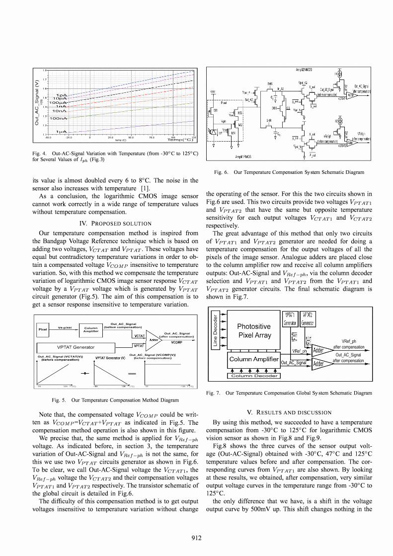
Fig. 4. Out-AC-Signal Variation with Temperature (from -30°C to 125°C) for Several Values of Iph (Fig.3)
its value is almost doubled every 6 to 8°C. The noise in the sensor also increases with temperature [1].
As a conclusion, the logarithmic CMOS image sensor cannot work correctly in a wide range of temperature values without temperature compensation.
IV. PROPOSE D SO LUTION
Our temperature compensation method is inspired from the Bandgap Voltage Reference technique which is based on adding two voltages, VCTAT and VPTAT. These voltages have equal but contradictory temperature variations in order to obtain a compensated voltage VCOMP insensitive to temperature variation. So, with this method we compensate the temperature variation of logarithmic CMOS image sensor response VCT AT
voltage by a VPT AT voltage which is generated by VPT AT
circuit generator (Fig.5). The aim of this compensation is to get a sensor response insensitive to temperature variation.
Vs-plxel I Column I (bef�r':ttc:;p��s
n��on) EJ I Amplifier
I I " ........... "'- Out AC Signal
�I A .... �fter c;:�mp�n sation)
1,-----------------,1 IVPrATVAdd er VCOMP VPTAT Generator r-
Out_AC_Signal (VCTAT(V» OuCAC_Slgnal (VCOMP(V»
� ... "'� & '�.-� -30 125 T("C) -30 1 25 (-C) -30 -125 T("C)
Fig. 5. Our Temperature Compensation Method Diagram
Note that, the compensated voltage VCOMP could be written as VCOMP=VCTAT+VPTAT as indicated in Fig.5. The compensation method operation is also shown in this figure.
We precise that, the same method is applied for VRej-ph
voltage. As indicated before, in section 3, the temperature variation of Out-AC-Signal and VRej-ph is not the same, for this we use two VPT AT circuits generator as shown in Fig.6. To be clear, we call Out-AC-Signal voltage the VCT AT1, the VRej-ph voltage the VCTAT2 and their compensation voltages VPT ATl and VPT AT2 respectively. The transistor schematic of the global circuit is detailed in Fig.6.
The difficulty of this compensation method is to get output voltages insensitive to temperature variation without change
912
Fig. 6. Our Temperature Compensation System Schematic Diagram
the operating of the sensor. For this the two circuits shown in Fig.6 are used. This two circuits provide two voltages VPT ATl
and VPT AT2 that have the same but opposite temperature sensitivity for each output voltages VCT ATl and VCT AT2
respectively. The great advantage of this method that only two circuits
of VPT ATl and VPT AT2 generator are needed for doing a temperature compensation for the output voltages of all the pixels of the image sensor. Analogue adders are placed close to the column amplifier row and receive all column amplifiers outputs: Out-AC-Signal and VRej-ph, via the column decoder selection and VPT ATl and VPT AT2 from the VPT ATl and VPT AT2 generator circuits. The final schematic diagram is shown in Fig.7.
Q; "0 o U Q) o Q) c :.J
Photositive
Pixel Array
Column Decoder
VRef.Jlh after compensation
Out_ AC _Signal after compensation
Fig. 7. Our Temperature Compensation Glo bal System Schematic Diagram
V. RESU LTS AN D DISCUSSION
By using this method, we succeeded to have a temperature compensation from -30°C to 125°C for logarithmic CMOS vision sensor as shown in Fig.8 and Fig.9.
Fig.8 shows the three curves of the sensor output voltage (Out-AC-Signal) obtained with -30°C, 47°C and 125°C temperature values before and after compensation. The corresponding curves from VPT ATl are also shown. By looking at these results, we obtained, after compensation, very similar output voltage curves in the temperature range from -30°C to 125°C.
the only difference that we have, is a shift in the voltage output curve by 500mV up. This shift changes nothing in the

-to"C 4rc ! 121c i 2.' -rrC 4rc I 12SiC f 1.75
� !l I I 1.5 f i f
� 2;1.25 f ! i 0» (jj I.' ,
I ,
I i , () .75
�30"C 470� 1 1S0C
5 i .,
:J , 0 I I I .25
• I I ! 10-15 10-14 10-13 10-12
i i I /�olJt_ACl-Signf3 1 (V) tjteL.cOfOpeO'ja.tJ.o.cL
i i ---� ! I
:----==t:::=n r---. i � f i i i , , i i I I , , I ,
! ! 10-11 10010
d¢(o�
- �f
''\. ' , S�I (V) I O.(.t AC�
I I i
I
!
Before cjmpe1satio
i I I , , I I I
'�� , ! pTAT1! 1009 10-8 10-7 10-6 1005
Iph(A)
Fig. 8. Results O btained With Our Compensation Scheme
sensor operation. Fig.9 shows the two curves of sensor output voltage Out
AC-Signal obtained without and with compensation scheme optimized for Iph=lnA. We conclude clearly that after compensation we obtained an output voltage curve that is insensitive to temperature variation.
L'
After co pensation L'
2 1.7 iii C
��1.0 -I
.----e � ensation
U <i L' r--�I --::l --0 L
L' -MoO -2�00 , 2�00 6000 1�00 '" '" 1<tmp(C)
Fig. 9. Compensated and Non Compcnsatcd Out-AC-Signal Curves for Iph=lnA (Fig.3)
Furthermore, we get a good temperature compensation, less than ImV of the output voltage temperature variation from -30°C to 125°C for Iph=lnA instead of 200m V However, when we move from this value we compensate less than in InA. Despite variations in slope, the compensation is well and we obtain less than 16mV from 45°C to 125°C instead of IIOmV, and less than 25mV from 45°C to -30°C instead of 165mV for Iph=lpA. As conclusion, the output voltage variation of the sensor is reduced at most by 96% and at least by 78%. Note that, the values obtained above are the temperature variation of the difference between the two output voltages Out-AC-Signal and VRej-ph from -30°C to 125°C.
Therefore, with this temperature compensation method, a response sensor insensitive to temperature variation is obtained. The main advantage of this method is that it conserves all characteristics of the logarithmic CMOS vision sensor, like dynamic range and pixel silicon area.
Concerning the sensor output reference voltage (VRej-ph) a good temperature compensation is obtained and the temperature variation is reduced by 92%. The reason of this, that the VRej-ph voltage it not depends with the photo current Iph as
913
is the cas with the Out-AC-Signal voltage.
V I. CONC LUSIONS AN D FUTURE WORK
A temperature compensation system dedicated to CMOS logarithmic image sensor has been presented. After an overview of logarithmic CMOS image sensor, the temperature effects on MOS transistor parameters like mobility /-Ln, threshold voltage vth and drain current IDS are introduced. Temperature effect results on logarithmic CMOS image sensor have been shown. We have been shown that the output voltage of the logarithmic CMOS image sensor varies strongly and linearly with temperature and it depends with photocurrent. A temperature compensation method is described and the associated results are shown. Through this compensation method, we have reduced strongly the temperature variation of the output voltages and we have a good temperature stability of the responses sensor (Out-AC-Signal and VRej-ph). The main advantage of this method is that it conserves the same sensor response characteristics like the high sensor dynamic range. In addition, it conserves pixel array silicon area and only two circuits to compensate all the output voltages Out-AC-Signal and VRej-ph of the sensor are used. Future works consist of designing a prototype of CMOS imager, which includes this temperature compensation scheme and the adaptation of this method for a standard integration pixel scheme.
V II. ACKNOW LE DGMENT
We would like to thank the VisImalogic project, and the "Pole de competivite" Minalogic which funds this research work.
REFERENCES
[I] A. EI Gamal and H. Eltoukhy, "Cmos image sensors," IEEE, Circuits and Devices Magazine, vol. 21, no. 3, pp. 6-20, May-June 2005.
[2] S. K. Mendis, S. E. Kcmeny, R. C. Gee, 8. Pain, C. O. Stallcr, Q. Kim, and E. R. Fossum, "Cmos active pixel image sensors for highly intcgrated imaging systems," IEEE Journal of Solid-State Circuits, vol. 32, no. 2, pp. 187-197, Fcb. 1997.
[3] E. La bonne, G. Sicard, and M. Renaudin, "An on-pixel fpn reduction method for a high dynamic rangc cmos imager," in , " in Proc. 33rd IEEE European Solid State Circuits Conference ESSCIRC'07, Munich, Germany, 2007, pp. 332-335.
[4] P. K. T. Mok and K. N. L., " Dcsign considerations of reccnt advanced low-voltage low-temperature-coefficient cmos bandgap voltage reference," in Proc. Custom Integrated Circuits Conference the IEEE 2004,
3-6 Oct. 2004, pp. 635-642. [5] D.-S. Min, D.-S. Jun, S. Cho, Y. Seok, Y. Kim, K.-R. Min, J. Han, J. Roh,
O. H. K won, D. Chin, and Y. E. Park, "Tcmpcrature-compcnsation circuit tcchniques for high-density cmos drams," in Proc. Digest of Technical Papers VLSI Circuits 1991 Symp, 1991, pp. 125-126.
[6] V. Sundc, Z. Bcncic, and Z. Jakopovic, "A tcmpcrature-dcpendent electrothcrmal mosfet model for calculating its current loada bility," in Proc. IEEE International Symposium on Industrial Electronics ISlE '99, vol. 2, 12-16 July 1999, pp. 579-583.
[7] F. Shoucair, " Design consideration in high temperature analog cmos integrated circuits," IEEE Transactions on Components, Hybrids, and Manufacturing Technology, vol. 9, no. 3, pp. 242-251, Sep 1986.
[8] A. J. David and K. M., Analog Integrated Circuit Design. John Wiley and Sons, Inc, 1997.
[9] E. A. Phillip and D. R. H., CMOS Analog Circuit Design. Oxford University Press, 2002.
[10] I. M. Filanovsky and A. Allam, "Mutual compensation of mo bility and threshold voltage tcmpcrature cffccts with applications in cmos circuits," IEEE Circuits and Systems, vol. 48, no. 7, pp. 876-884, July 2001.