terahertz single pixel imaging with an optically controlled dynamic spatial light modulator
TRANSCRIPT

Terahertz single pixel imaging with anoptically controlled dynamic spatial light
modulator
David Shrekenhamer, Claire M. Watts, and Willie J. Padilla�
Department of Physics, Boston College, 140 Commonwealth Ave., Chestnut Hill, MA 02467,USA
Abstract: We present a single pixel terahertz (THz) imaging techniqueusing optical photoexcitation of semiconductors to dynamically and spa-tially control the electromagnetic properties of a semiconductor mask tocollectively form a THz spatial light modulator (SLM). By co-propagatinga THz and collimated optical laser beam through a high-resistivity siliconwafer, we are able to modify the THz transmission in real-time. By furtherencoding a spatial pattern on the optical beam with a digital micro-mirrordevice (DMD), we may write masks for THz radiation. We use masksof varying complexities ranging from 63 to 1023 pixels and are able toacquire images at speeds up to 1/2 Hz. Our results demonstrate the viabilityof obtaining real-time and high-fidelity THz images using an opticallycontrolled SLM with a single pixel detector.
© 2013 Optical Society of America
OCIS codes: (110.6795) Terahertz imaging; (160.3918) Metamaterials; (070.6120) Spatiallight modulators; (110.1085) Adaptive imaging.
References and links1. D. M. Mittleman, M. Gupta, R. Neelamani, R. G. Baraniuk, J. V. Rudd, and M. Koch, “Recent advances in
terahertz imaging,” Appl. Phys. B 68, 1085–1094 (1999).2. W. L. Chan, J. Deibel, and D. M. Mittleman, “Imaging with terahertz radiation,” Rep. on Prog. in Phys. 70,
1325–1379 (2007).3. T. M. Korter and D. F. Plusquellic, “Continuous-wave terahertz spectroscopy of biotin: vibrational anharmonicity
in the far-infrared,” Chem. Phys. Lett. 385, 45–51 (2004).4. N. Karpowicz, H. Zhong, C. Zhang, K. -I. Lin, J. -S. Hwang, J. Xu, and X. -C. Zhang, “Compact continuous-wave
subterahertz system for inspection applications,” Appl. Phys. Lett. 86, 054105 (2005).5. K. Kawase, Y. Ogawa, Y. Watanabe, and H. Inoue, “Non-destructive terahertz imaging of illicit drugs using
spectral fingerprints,” Opt. Express 11, 2549 (2003).6. G. P. Williams, “Filling the THz gap – high power sources and applications,” Rep. Prog. Phys. 69, 301–326
(2005).7. A. W. Lee, and Q. Hu, “Real-time, continuous-wave terahertz imaging by use of a microbolometer focal-plane
array,” Opt. Lett. 30, 2563–2565 (2005).8. N. R. Butler, R. J. Blackwell, R. Murphy, R. J. Silva, and C. A. Marshall, “Low-cost uncooled microbolometer
imaging system for dual use,” Proc. SPIE 2552 583–591 (1995).9. Q. Wu, T. D. Hewitt, and X. -C. Zhang, “Two-dimensional electro-optic imaging of THz beams,” Appl. Phys.
Lett. 69, 1026–1028 (1996).10. B. B. Hu and M. C. Nuss, “Imaging with terahertz waves,” Opt. Lett. 20, 1716–1718 (1995).11. M. C. Nuss, “Chemistry is right for T-ray imaging,” IEEE Circ. Dev. Mag., 12, 25–30 (1996).12. W. L. Chan, K. Charan, D. Takhar, K. F. Kelly, R. G. Baraniuk, and D. M. Mittleman, “A single-pixel terahertz
imaging system based on compressed sensing,” Appl. Phys. Lett. 93, 121105 (2008).13. O. Furxhi, E. L. Jacobs, and C. Preza, “Image plane coded aperture for terahertz imaging,” Opt. Eng. 51, 091612
(2012).
#187520 - $15.00 USD Received 21 Mar 2013; revised 5 May 2013; accepted 7 May 2013; published 14 May 2013(C) 2013 OSA 20 May 2013 | Vol. 21, No. 10 | DOI:10.1364/OE.21.012507 | OPTICS EXPRESS 12507

14. H. Shen, L. Gan, N. Newman, Y. Dong, C. Li, Y. Huang, and Y. Shen, “Spinning disk for compressive imaging,”Opt. Lett. 37, 46–48 (2012).
15. D. Dudley, W. Duncan, and J. Slaughter, “Emerging digital micromirror device (DMD) applications,” Proc. SPIE4985, 14–25 (2003).
16. K. M. Johnson, D. J. McKnight, and I. Underwood, “Smart spatial light modulators using liquid crystals onsilicon,” IEEE J. Quantum Electron. 29, 699–714 (1993).
17. M. Rahm, J. Li, and W. J. Padilla, “THz wave modulators: a brief review on different modulation techniques,” J.Infrared Millim. Terahz. Waves 34, 1–27 (2012).
18. W. L. Chan, H. -T. Chen, A. J. Taylor, I. Brener, M. J. Cich, and D. M. Mittleman, “A spatial light modulator forterahertz beams,” Appl. Phys. Lett. 94, 213511 (2009).
19. D. Shrekenhamer, S. Rout, A. C. Strikwerda, C. Bingham, R. D. Averitt, S. Sonkusale, and W. J. Padilla, “Highspeed terahertz modulation from metamaterials with embedded high electron mobility transistors,” Opt. Express19, 9968–9975 (2011).
20. G. W. Webb, W. Vernon, M. Sanchez, S. Rose, and S. Angello, “Optically controlled millimeter wave antenna,”Microw. Photon. 275–278 (1999).
21. M. R. Chaharmir, J. Shaker, M. Cuhaci, and A. Sebak, “Novel photonically-controlled reflectarray antenna,”IEEE Trans. Antennas Propag. 54, 1134–1141 (2006).
22. X. C. Zhang and D. Auston, “Generation of steerable submillimeter waves from semiconductor surfaces byspatial light modulators,” Appl. Phys. Lett. 59, 768–770 (1991).
23. T. Okada and K. Tanaka, “Photo-designed terahertz devices,” Sci. Rep. 1, 121 (2011).24. S. Busch, B. Scherger, M. Scheller, and M. Koch, “Optically controlled terahertz beam steering and imaging,”
Opt. Lett. 37, 1391–1393 (2012).25. M. Harwit and N. J. Sloane, Hadamard Transform Optics (Academic, 1979).26. W. Cheney and D. Kincaid, Numerical Mathematics and Computing, 6th ed. (Thompson Brooks/Cole, 2008).27. R. H. Bube, Photoelectronic Properties of Semiconductors, (Cambridge University, 1992).28. D. Cooke and P. U. Jepsen, “Optical modulation of terahertz pulses in a parallel plate waveguide,” Opt. Express
16, 15123–15129 (2008).29. M. Van Exter and D. Grischkowsky, “Optical and electronic properties of doped silicon from 0.1 to 2 THz,”
Appl. Phys. Lett. 56, 1694–1696 (1990).30. H. Alius and G. Dodel, “Amplitude-, phase-, and frequency modulation of far-infrared radiation by optical exci-
tation of silicon,” Infrared Phys. 32, 1–11 (1991).31. T. Jeon and D. Grischkowsky, “Nature of conduction in doped silicon,” Phys. Rev. Lett. 78, 1106–1109 (1997).32. H. Schulenburg and H. Tributsch, “Electropassivation of silicon and bulk lifetime determination with dry polymer
contact,” J. Phys. D 33, 851 (2000).33. C. Hutley, Diffraction Gratings, (Academic, 1982).34. J. P. Rice, J. E. Neira, M. Kehoe, and R. Swanson, “DMD diffraction measurements to support design of pro-
jectors for test and evaluation of multispectral and hyperspectral imaging sensors,” Proc. SPIE 7210, 72100D(2009).
35. E. L. Shirley, “Diffraction effects on broadband radiation: formulation for computing total irradiance,” Appl. Opt.43, 2609–2620 (2004).
36. C. A. Bennet, Principles of Physical Optics (John Wiley & Sons, 2008).37. W. J. Padilla, A. J. Taylor, C. Highstrete, M. Lee, and R. D. Averitt, “Dynamical electric and magnetic metama-
terial response at terahertz frequencies,” Phys. Rev. Lett. 96, 107401 (2006).38. H. -T. Chen, W. J. Padilla, M. J. Cich, A. K. Azad, R. D. Averitt, and A. J. Taylor, “A metamaterial solid-state
terahertz phase modulator,” Nat. Photonics 3, 148–151 (2009).39. H. Chen, J. F. O’Hara, A. J. Taylor, R. D. Averitt, C. Highstrete, M. Lee, and W. J. Padilla, “Complementary
planar terahertz metamaterials,” Opt. Express 15, 1084–1095 (2007).40. R. A. DeVerse, R. R. Coifman, A. C. Coppi, W. G. Fateley, F. Geshwind, R. M. Hammaker, S. Valenti, F. J.
Warner, and G. L. Davis, “Application of spatial light modulators for new modalities in spectrometry and imag-ing,” Proc. SPIE 4959, 12–22 (2003).
1. Introduction
Terahertz (THz) radiation has great potential for imaging applications [1,2] due to its ability topenetrate most dielectric materials and non-polar liquids. Its harmless interaction with humantissue suggests imaging in this regime has immediate applicability in the fields of biodetec-tion [3], system inspection [4], and detection of illegal drugs [5]. However, a significant lim-itation currently preventing wide-spread THz imaging is the absence of efficient sources anddetectors operating between 0.1 and 10 THz - a band of the electromagnetic spectrum oftenreferred to as the “THz gap” [6]. Although there exists great technical difficulty in feasibly
#187520 - $15.00 USD Received 21 Mar 2013; revised 5 May 2013; accepted 7 May 2013; published 14 May 2013(C) 2013 OSA 20 May 2013 | Vol. 21, No. 10 | DOI:10.1364/OE.21.012507 | OPTICS EXPRESS 12508

performing THz imaging, there has been moderate progress over the past 25 years. Multi-element detector schemes, both microbolometer arrays [7, 8] and electro-optic sampling withhigh-performance CCD cameras [9], provide accurate and real-time THz images. However,these imaging systems often require high powered sources and/or expensive complex detectorsthat lack the sensitivity of single element detectors. The use of a single detector has been em-ployed to obtain THz images by mechanically raster scanning the object plane to acquire spatialinformation [10]. While the latter technique has the benefit of high spatial resolution and accu-rate imaging, major shortcomings are the long acquisition time [11] and the mechanical natureof the scanning system.
An alternative single pixel solution - relying on spatial multiplexing - could help overcomemany of the disadvantages involved with more conventional imaging techniques. The imagingof complex scenes is enabled with sparse detector arrays or even single pixels using spatiallight modulators (SLMs) to multiplex the image. Mechanical masks that are either manuallyexchanged or placed onto spinning discs have demonstrated proof of principle THz imagingusing, for example, compressive sensing and adaptive coded aperture imaging [12–14]. Al-though SLMs, such as digital micro-mirror (DMD) [15] and liquid crystal (LC) [16] systemsare commercially available, they do not operate at THz frequencies. Attempts to develop THzSLMs have thus far been ineffective in producing efficient and high speed devices, though thereare several attractive alternatives to using mechanical masks.
Semiconductor and metamaterial / semiconductor hybrid devices can be controlled by a va-riety of different methods to achieve THz amplitude and frequency modulation [17]. An initialstudy demonstrated performance of a room-temperature electronic controlled metamaterial fora 4×4 pixel array used to form a diffractive grating [18]. Additionally, all-electronic dynamicmetamaterials have demonstrated switching speeds up to 10 MHz [19]. Another avenue toachieving a THz SLM has been inspired by the work initially developed at millimeter wave-lengths where optically excited electron plasmas in photo-active semiconductors serve as aspatial mask in creating Fresnel lenses and reflect-arrays for beam-steering and communicationbased applications [20, 21]. Early studies indicate that THz spatial modulation is also possiblewith sufficient optical power [22–24]. Both electronic and optically controlled SLMs pose asa fast and efficient means to dynamically control electromagnetic radiation thus allowing forrealistic methods to perform THz imaging.
In this work we demonstrate single pixel multiplex THz imaging based on an optically con-trolled reconfigurable THz mask in high-resistivity Silicon (ρ-Si). By utilizing a DMD to opti-cally encode spatial patterns we are able to achieve up to 1023-pixel, high fidelity THz imageswith frame rates as fast as one image per two seconds - only limited by available software. Theachieved signal-to-noise ratio (SNR) suggests the possibility that our technology may providequasi real-time THz imaging with frame rates as fast as 3 frames per second (fps).
2. Theory
2.1. Imaging theory
Typical single pixel camera architectures involve four key components: a light source, imagingoptics, a single element detector, and a SLM. Light from an illuminated object is focused usingimaging optics onto a SLM which, for binary encoding, selectively passes portions of the imageto the detector and blocks others. A sequence of known patterns is displayed on the SLM anda single value is acquired for each mask frame. Prior knowledge of these masks allows forthe reconstruction of the image as schematically illustrated in Fig. 1. For example, mechanicalraster scanning can be emulated by displaying a single pixel at a time on the SLM.
For imaging systems using intensity based detectors that are not sensitive to the phase of elec-tromagnetic radiation, binary masks that modulate the intensity are well suited. There are sev-
#187520 - $15.00 USD Received 21 Mar 2013; revised 5 May 2013; accepted 7 May 2013; published 14 May 2013(C) 2013 OSA 20 May 2013 | Vol. 21, No. 10 | DOI:10.1364/OE.21.012507 | OPTICS EXPRESS 12509

Object Image on SLM X
Measurements Y
y1
y2
y1
y2
yM
... =
x1
x2
xN
...
Masks of SLM make up rows of measurement matrix
Φ
Reconstruction: X = Φ Y-1
yM
...
Fig. 1. Schematic depicting multiplex imaging process where the spatial modulation of aformed image allows for the reconstruction using a single pixel detector. Example 7× 9binary masks taken from rows of the 63×63 S-matrix are shown.
eral different types of binary coded apertures that can be used to multiplex an image - though thefield is dominated by random and Hadamard based masks. Random binary masks are comprisedof 1’s and 0’s determined by standard probability distributions such as Gaussian or Bernoulli,among others. Hadamard matrices are square matrices composed of +1’s and -1’s in which eachrow is orthogonal to all other rows [25]. To create binary masks we can use an S-matrix, cre-ated by omitting the first row and column of the corresponding normalized Hadamard matrix,substituting all 1’s with 0’s, and all -1’s with 1’s. Each row of this matrix can then be used as a1, 0 mask for successive measurements in a single pixel imaging system.
We define a one- or two- dimensional image by a vector X with N-elements (this can be doneby concatenating the rows into a single column). We represent a single measurement y j in amultiplexing scheme by the following expression:
y j =N
∑i=1
φ jixi (1)
or the matrix equation Y = Φ×X . In this equation, Y is a column vector with M-elementsrepresenting the M measurements taken and Φ is the M×N measurement matrix, in whicheach row represents a mask displayed on the SLM. For example, Φ that corresponds to a rasterscan imaging technique is the N ×N identity matrix. For a well-conditioned measurement ma-trix [26] and the fully determined case, i.e. M = N, the reconstruction becomes linear and canbe solved by a simple matrix equation: X = Φ−1 ×Y [25]. One advantage of using S-matricesas the measurement matrix such that Φ = SN is the particularly simple decoding process givenby: S−1
N = 2N+1 (2ST
N − JN) where SN is the S-matrix of order N, STN is its transpose, and JN is an
N ×N matrix of all 1’s [25].
2.2. Dynamic THz spatial light modulators
The photoexcitation of free carriers in semiconductors is a well understood process for both CWand ultrafast optical beams [27]. For ρ-Si substrates a higher carrier density can be generated byCW pump beams, compared to pulsed sources of identical average power, due to the relativelylong carrier lifetimes in Si [28]. The change in the complex dielectric constant can be describedby the Drude model [28–31].
ε(ω) = ε∞ − ω2p
ω(ω + iΓ), (2)
#187520 - $15.00 USD Received 21 Mar 2013; revised 5 May 2013; accepted 7 May 2013; published 14 May 2013(C) 2013 OSA 20 May 2013 | Vol. 21, No. 10 | DOI:10.1364/OE.21.012507 | OPTICS EXPRESS 12510

Tran
smis
sion
Frequency (THz)
0 255 1000
Fluence (mW/cm2) 0.17 2.5 6.0
nSi ( x1015 cm-3)
0.2
0.4
0.6
0.8
1.0
1.10.7 1.5 1.9 2.3
Diff
eren
tial T
rans
mis
sion
Frequency (THz)
255 1000
Fluence (mW/cm2) 2.5 6.0
nSi ( x1015 cm-3)-0.45
-0.30
-0.15
0.00
0.15
1.10.7 1.5 1.9 2.3
a) b)
Fig. 2. (a) Solid curves show the transmission of THz radiation through ρ-Si wafer as afunction of frequency for several different optical fluence values. Measurements were donein atmosphere in FTIR system. The dashed curves show the simulated fits for increasingcarrier concentration nSi within the penetration depth (85 μm) of ρ-Si. (b) Dependence ofthe differential transmission on the optical fluence as defined in the text.
where ε∞ = 11.7 is the frequency independent dielectric permittivity due to the contributionof bound electrons, Γ = 1/τc is the damping rate (with τc = 160 fs the average collisiontime [28, 31]), ω2
p is the plasma frequency defined as ω2p = nSie2/ε0m∗ with e the electron
charge, ε0 the free-space permittivity, and m∗ = 0.26me the effective mass [31]. If we neglectthe carrier diffusion and consider only free carrier generation and linear recombination in thesemiconductor, the carrier density nSi is proportional to the optical power of the pump beamand is modulated through photodoping [30]
nSi =I0(1−R)τ
2Adh̄ω, (3)
where I0 is average power, R is the reflectivity of Si at the pump wavelength, h̄ω is the photonenergy, τ = 25 μs is the carrier lifetime [32], A is the area of the laser excitation, and d is thepenetration depth. At THz frequencies the photodoped charges correspond to a large increasein the absorption coefficient as a function of I0, allowing for strong attenuation of incident THzelectromagnetic waves.
We measured the THz transmission, shown as the solid curves in Fig. 2, through a 520μm thick ρ-Si substrate (ρ > 10,000 ohm-cm) for increasing optical power using a 980 nmCW laser diode. We characterize the THz transmission using a Fourier Transform Infrared(FTIR) spectrometer, a mercury (Hg) arc lamp source, multi-layer mylar beamsplitter, andliquid-helium cooled silicon bolometer. The size of the THz and optical beams was 4mmand 9mm, respectively, at the plane where we placed the ρ-Si substrate. Etalons due to mul-tiple reflections within the ρ-Si substrate were removed and the modified interferogram wasFourier transformed to obtain the sample spectrum. A similar procedure was performed fora reference with an open channel; division of the sample and reference spectra resulted in thefrequency dependent absolute value transmission T(ω) and corresponding differential transmis-sion [Tp(ω)−Tp=0(ω)]/Tp=0(ω) shown in Figs. 2(a) and 2(b), respectively. We observe broad-band attenuation of the THz signal where, at our maximum fluence of p = 1 W/cm2, we measurea modulation depth of 43% at 0.7 THz. The undoped (Tp=0(ω), black curve) of Fig. 2(a) wasperformed in vacuum; however, due to technical limitations, transmission measurements forboth photodoped cases were performed in air - leading to a reduced signal-to-noise which ac-
#187520 - $15.00 USD Received 21 Mar 2013; revised 5 May 2013; accepted 7 May 2013; published 14 May 2013(C) 2013 OSA 20 May 2013 | Vol. 21, No. 10 | DOI:10.1364/OE.21.012507 | OPTICS EXPRESS 12511
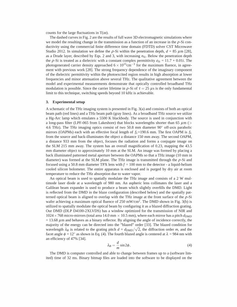
counts for the large fluctuations in T(ω).The dashed curves in Fig. 2 are the results of full wave 3D electromagnetic simulations where
we model the resulting change in the transmission as a function of an increase in the ρ-Si con-ductivity using the commercial finite difference time domain (FDTD) solver CST MicrowaveStudio 2012. In simulation we define the ρ-Si within the penetration depth, d = 85 μm [28],as a Drude layer, described by Eqs. 2 and 3, with increasing nSi. Below the penetration depththe ρ-Si is treated as a dielectric with a constant complex permittivity εSi = 11.7 + 0.01i. Thephotogenerated carrier density approached 6× 1015cm−3 for the maximum fluence, in agree-ment with previous work [28]. The strong frequency dependence of the imaginary componentof the dielectric permittivity within the photoexcited region results in high absorption at lowerfrequencies and minor attenuation above several THz. The qualitative agreement between themodel and experimental measurements demonstrate that optically controlled broadband THzmodulation is possible. Since the carrier lifetime in ρ-Si of τ = 25 μs is the only fundamentallimit to this technique, switching speeds beyond 10 kHz is achievable.
3. Experimental setup
A schematic of the THz imaging system is presented in Fig. 3(a) and consists of both an opticalbeam path (red lines) and a THz beam path (gray lines). As a broadband THz source we utilizea Hg-Arc lamp which emulates a 5500 K blackbody. The source is used in conjunction witha long-pass filter (LPF-065 from Lakeshore) that blocks wavelengths shorter than 65 μm (>4.6 THz). The THz imaging optics consist of two 50.8 mm diameter 90◦ off-axis parabolicmirrors (OAPMs) each with an effective focal length of fL=190.6 mm. The first OAPM is fLfrom the source and back-illuminates the object a distance 150 mm away. The second OAPM,a distance 933 mm from the object, focuses the radiation and forms a conjugate image onthe SLM 215 mm away. The system has an overall magnification of 0.23, mapping the 43.5mm diameter object to approximately 10 mm at the SLM. An image was formed by placing aback illuminated patterned metal aperture between the OAPMs so that a THz image (10 mm indiameter) was formed at the SLM plane. The THz image is transmitted through the ρ-Si andfocused using a 50.8 mm diameter TPX lens with f = 100 mm to the detector - a liquid-heliumcooled silicon bolometer. The entire apparatus is enclosed and is purged by dry air at roomtemperature to reduce the THz absorption due to water vapor.
An optical beam is used to spatially modulate the THz image and consists of a 2 W mul-timode laser diode at a wavelength of 980 nm. An aspheric lens collimates the laser and aGalilean beam expander is used to produce a beam which slightly overfills the DMD. Lightis reflected from the DMD in the blaze configuration (described below) and the spatially pat-terned optical beam is aligned to overlap with the THz image at the front surface of the ρ-Siwafer achieving a maximum optical fluence of 250 mW/cm2. The DMD shown in Fig. 3(b) isutilized to spatially modulate the optical beam by configuring it as a blazed diffraction grating.Our DMD (DLP D4100-2XLVDS) has a window optimized for the transmission of NIR and1024×768 micro-mirrors (total area 14.0 mm × 10.5 mm), where each mirror has a pitch dDMD
= 13.68 μm and behaves as a binary reflector. By aligning the angle of incidence correctly, themajority of the energy can be directed into the ”blazed” order [33]. The blazed condition forwavelength λB is related to the grating pitch d = dDMD/
√2, the diffraction order m, and the
facet angle φ = 12◦ as shown in Eq. (4). The fourth blazed angle is centered at λ = 984 nm withan efficiency of 47% [34].
λB =dm
sin2φ , (4)
The DMD is computer controlled and able to change between frames up to a (software lim-ited) time of 32 ms. Binary bitmap files are loaded into the software to be displayed on the
#187520 - $15.00 USD Received 21 Mar 2013; revised 5 May 2013; accepted 7 May 2013; published 14 May 2013(C) 2013 OSA 20 May 2013 | Vol. 21, No. 10 | DOI:10.1364/OE.21.012507 | OPTICS EXPRESS 12512

Off Axis Parabolic Mirror (OAPM)
OAPM
Digital Micromirror Device
Object to be Imaged
THz Source - Hg-Arc Lamp
980nm Collimated LED Source
BolometerTHz Detector
High-Resistivity Silicon
f = 100mm TPX lens
10x Beam Expander
Arbitrary Waveform Generator
THz beam path
Optical LED beam path
...
Lock-In AmplifierStanford Research Systems SR830
a) b)
0.50.0 1.0 1.5 2.0
50
75
100
125
Volta
ge (m
V)
40 80 120 160
60
70
80
100
Volta
ge (m
V) Voltage (m
V)
Time (ms)Time (s)
c) d)
Reference
58.5 ± 0.5362.5 ± 0.27
71.0 ± 0.37
83.5 ± 0.25
Fig. 3. (a) Schematic of LED and THz optical layouts. The THz beam (shown in gray)passes through the object and is imaged with the OAPMs onto a ρ-Si wafer. The collimated980 nm wavelength optical beam (shown in red) reflects off the DMD surface and creates aspatial light pattern at the THz image plane. (b) Photograph of a 7×9 S-matrix mask patterndisplayed on DMD; each mask pixel is 1.5 mm being constructed from tiling 109× 109DMD pixels. (c) Lock-in amplifier voltage output is displayed as a function of time inseconds for the 63 sequential S-matrix masks; the entire measurement takes approximately2 s. Inset: reconstructed THz beam profile at image plane. (d) Zoom-in of time data shownin (c). Raw data from four consecutive S-matrix mask measurements are shown with thecorresponding binary mask shown above; the averaged values used for reconstruction alongwith the standard deviation are shown on the right.
#187520 - $15.00 USD Received 21 Mar 2013; revised 5 May 2013; accepted 7 May 2013; published 14 May 2013(C) 2013 OSA 20 May 2013 | Vol. 21, No. 10 | DOI:10.1364/OE.21.012507 | OPTICS EXPRESS 12513

DMD. The white portions represent light that was directed toward the ρ-Si whereas black rep-resents light that was directed away. This corresponds to white mask regions photodoping theρ-Si, i.e. modulating the THz transmission where black represents unmodulated regions. Sincethe DMD is designed for much shorter optical wavelengths, we may utilize several mirror pix-els to function as a single THz-sized pixel for the S-matrix mask, thus permitting flexibilityfor both pixel count and pitch. We use S-matrix masks of varying complexity and change thepixel size accordingly to keep the overall mask area approximately equal. The THz image res-olutions we investigated are summarized in Table 1 and the relation between physical size andDMD pixels is detailed.
Table 1. Relationship between THz imaging resolution and DMD pixel sizes
Order (N) Resolution THz Pixel Size DMD Pixels / THz Pixel
63 7×9 1.5 mm × 1.5 mm 109×109
255 15×17 698 μm × 698 μm 51×51
1023 31×33 328 μm × 328 μm 24×24
Detection of the THz signal is performed with a lock-in detection technique. The laser diodepower is modulated with a square wave at a frequency of 300 Hz, which in turn modulatesthe THz power detected. Output voltage from the Si-bolometer is input into a lock-in amplifierwhich provides the measured THz signal in Volts. Figures 3(c), 3(d) show the measured lock-in voltage as a function of time for several successive masks; the corresponding binary bitmapdisplayed on the DMD are shown above the raw data in Fig. 3(d). The stabilization of thelock-in signal after switching between masks is close to 5 ms, with a SNR recorded for eachmeasurement greater than 100; this is sufficient to allow us to acquire a THz measurement atthe limits of the switching time of the DMD. We may estimate the total power of THz radiationused in our imaging apparatus since our bolometer has a calibrated responsivity of 2.64×10⁵
V/W at 300 Hz. Our DMD may be configured to modulate all pixels on and off, from which wemeasure a lock-in signal of 130 mV. Thus our THz image consists of a maximum modulatedTHz power of 96 nW over an integrated bandwidth from 0.2 - 4.6 THz.
4. Experimental results and discussion
Using the experimental apparatus shown in Fig. 3 we performed single pixel THz imaging ofvarious scenes. All THz images are normalized by referencing to the beam profile with noobject present. The flexibility afforded by our setup enabled us to image at many differentmask resolutions and sizes without physically changing the system. Figure 3(c) shows the THzsignal for 63 different S-matrix masks displayed over a period of 2 s (each mask is displayed forapproximately 32 ms). Figure 3(d) shows zoomed-in raw data for consecutive S-matrix masks,with the corresponding binary mask shown above and the average value used for reconstructionshown in red on the right axis. The inset to Fig. 3(c) shows a false color image of the THz beamprofile at the image plane. The reconstruction was done using 63 measurements from the 7×9S-matrix masks (pixel size 1.5 mm) with the total measurement time of approximately 2 s. It isclear from the data shown that quality THz images can be acquired in relatively short times. Asstated, the current limitation on speed is software related resulting in mask modulation speedof approximately 31 Hz. However, the response time of the system to a change in mask isapproximately 5 ms, resulting in a potential frame rate of 3 fps.
In order to compare our imaging system to more conventional schemes, we perform bothraster scan and Hadamard imaging and highlight differences between the two methods - see
#187520 - $15.00 USD Received 21 Mar 2013; revised 5 May 2013; accepted 7 May 2013; published 14 May 2013(C) 2013 OSA 20 May 2013 | Vol. 21, No. 10 | DOI:10.1364/OE.21.012507 | OPTICS EXPRESS 12514

2 mm1 cm
Raster Scan Image Hadamard ImageOptical Image
7x9 Imag
e15x17 Im
age
31x33 Imag
e
c)
d)
e)
f )
g)
h)
b)
Metallic Aperture
a)
i)
20.0
1.0
2.0
2
4
6
8
10
4 6 8 10
x -axis (mm)
y -a
xis
(mm
)
THz Po
wer D
ensity (n
W/m
m2)
-3 dB-6 dB
-9 dB
Fig. 4. Comparison of THz imaging with raster scan masks and S-matrix masks. (a,b) Showthe metallic aperture used as the object and the conjugate optical image on the ρ-Si wafer.(c) Spatial map of the THz power density shown for the reference beam profile with contourplots showing the intensity drop in dB. (d) - (f) Shows raster-scan images for increasingmask complexity. (g) - (i) Shows Hadamard reconstructed images of the same size andcomplexity as the raster scan measurements to the immediate left. Each mask was displayedfor 500 ms for all above measurements.
Fig. 4. S-matrix masks consist of roughly 50% light throughput and it has been demonstratedthat using masks created from an N ×N S-matrix can increase SNR by a factor of (N+1)
2√
N∼=
√N
2over raster scan imaging with the same resolution and pixel size [25]. Figsures 4(a), 4(b) showboth the metallic aperture used as an object and an optical photograph of the conjugate imageat the front surface of the ρ-Si wafer. It is well known that aspheric optics, such as OAPMs,produce aberrations that can distort the image plane in the form of astigmatism and coma, asseen by the image distortion in Fig. 4(b) [36].
Figures 4(c) – 4(e) show raster-scan images acquired with increasing resolution and con-structed from 63, 255, and 1023 measurements respectively. The last column in Fig. 4(f) – 4(h)shows Hadamard reconstructions with the same number of measurements and resolution as theraster scan images. In order to compare different imaging techniques and resolutions, an iden-tical time of 500 ms per mask was used, giving total acquisition times of 31.5 s for the 7× 9images, 127.5 s for the 15× 17 images, and 511.5 s for the 31× 33 images. While the imagequality in the case of 7× 9 pixel resolution is comparable between the two techniques, therapid decrease in image quality for the raster scan images at higher resolutions is apparent - seeFig. 4(e). In contrast, the image quality is retained for increasing pixel count in the multiplexingcase.
To better understand why the signal depreciated significantly for increasing pixel complexityin the case of the raster scan we investigated the measured power for each respective masktype. We calculate the spatial dependence of the power density (nW/mm2) by taking the totalmeasured THz power (96 nW) and extracting the THz power density per pixel pi from the
#187520 - $15.00 USD Received 21 Mar 2013; revised 5 May 2013; accepted 7 May 2013; published 14 May 2013(C) 2013 OSA 20 May 2013 | Vol. 21, No. 10 | DOI:10.1364/OE.21.012507 | OPTICS EXPRESS 12515

a) d)c)b)
e) h)g)f )
Fig. 5. THz imaging with high-resolution S-matrix masks (31× 33 pixels with each pixelmeasuring 328 μm on a side). (a,b) Show metallic apertures used as the object of twodifferently sized crosses, with arm widths of approximately 8 mm and 4.5 mm in the objectplane mapping to 2.5 mm and 1.5 mm on the image plane. (c,d) Two different types of metalrazor blades that were placed in manila envelopes for imaging. (e) - (h) Shows the THzimages of the corresponding objects shown immediately above. Each mask was displayedfor 500 ms for all measurements above, giving a total acquisition time of 511.5 s for eachimage.
measured 15×17 beam profile intensity as defined by
pi =96nW
(698μm)2 × xi
∑255i=1 xi
, (5)
where xi is the reconstructed signal from pixel i. In Fig. 4(i) we show a high quality image ofthe power density - sufficient to observe optical aberrations resulting from the use of OAPMswhich result in an asymmetric distribution of THz power about the horizontal axis, as men-tioned above. The power/pixel decreases for increasing resolution since the pixel size is re-duced - in our case from 1.5 mm to 698 μm to 328 μm. The peak power density calculated inEq. (5) is 2.5 nW/mm2 near the center of the beam. This corresponds to a total of 5.6 nW ofmeasured power for the 1.5 mm size pixel and 0.27 nW for the 328 μm pixel, a 95% reductionof measured power proportional to the decrease in pixel area. As shown in Fig. 4(i), the powerdensity is -9 dB lower towards the outer diameter of the images and approaches values as lowas 50 pW of THz power for 328 μm sized pixels - still well above the bolometer’s specifiednoise-equivalent-power (NEP) of 1.57× 10⁻¹³ W/
√Hz. The raster scan is unable to compen-
sate for the loss in measured signal for each pixel due to decreasing pixel dimension. In theHadamard case, although the signal per pixel also drops with decreasing pixel size, the increasein sampled pixels for each data acquisition offsets the reduction in signal. Consequently, thehigher resolution image offers more information without sacrificing SNR. The improvement inthe image quality for increasing pixel complexity is evident and allows for the aberrations ofthe THz image resulting from the OAPMs to be rendered.
In order to explore our imaging technique for possible use in screening applications, in Fig. 5we show various examples of high-fidelity THz images. The top row displays photographs ofall the objects imaged: crosses with 8 mm and 4.5 mm wide arms at the object plane (Fig. 5(a),5(b)) and two razor blades imaged in manila envelopes (Fig. 5(c), 5(d)). As stated above, wecan program the S-matrix masks to allow for several different functions and mask complexities.
#187520 - $15.00 USD Received 21 Mar 2013; revised 5 May 2013; accepted 7 May 2013; published 14 May 2013(C) 2013 OSA 20 May 2013 | Vol. 21, No. 10 | DOI:10.1364/OE.21.012507 | OPTICS EXPRESS 12516

We achieved high resolution images containing 31×33 pixels with each mask pixel measuring328 μm across; this was acquired with 1023 sequential measurements. Like the images shownin Fig. 4, the masks were displayed for 500 ms each, giving a total image acquisition time of511.5 s. The reconstructed THz images are shown in Fig. 5(e) – 5(h). Due to the magnificationof the system, the crosses are imaged down to have 2.5 mm and 1.5 mm wide arms, respec-tively. The minimum feature size of the images that we can resolve for these crosses is limitedby diffraction. The Rayleigh criterion suggests we achieve a diffraction limited spot size of ap-proximately 1.4 mm at 1 THz, although the inherently broadband nature of detected radiationpresented here generates a more complex diffraction pattern than that for use of a monochro-matic source [35]. The razor blades are placed within manila envelopes and are, obviously,not visible in the optical, however are clearly identified in the THz images, demonstrating thepotential for THz imaging to be used in security applications.
5. Metamaterial SLMs
Results presented in Figs. 4, 5 demonstrate the ability to perform THz imaging using a singlepixel detector. For many potential applications it would be desirable to obtain spectral informa-tion, rather than integrating across a portion of the THz range. As discussed in the introduction,metamaterials have shown an ability to modulate THz electromagnetic radiation with demon-strated advantages over conventional materials, including spectral selectivity, amplitude modu-lation [37], and phase modulation [38]. We computationally explore a metamaterial based SLMwhich is optically controlled - schematically shown Fig. 6(a). Our metamaterial SLM is mod-eled similar to that for the ρ-Si and we add a complimentary electric split ring resonator [39] tothe top of the substrate. The optically excited charge carriers shunt the resonant response of themetamaterial, effectively modulating the transmission at the operational frequency as shownin Figs. 6(b) and 6(c). The metamaterial has been designed to yield a band-pass response cen-tered at 1 THz and achieves a simulated modulation depth of 67% for a maximum fluence of 1W/cm2 - see Fig. 6(b).
The advantage in THz imaging provided by adding resonant metamaterials, as demonstratedin Fig. 6, is an increase in modulation depth at selected frequencies over bare silicon (67% ascompared to 37% at 1 THz). The modulation depth could be further improved by optimizingthe geometry of ρ-Si within the metamaterial unit cell, as well as the photodoping wavelength- both of which could potentially maximize the carrier density closer to the surface. Obtainingspectral information with conventional instruments can be challenging, requiring complex highcost equipment and instrumentation with significantly limited acquisition speeds [40]. By ar-ranging the pixels of metamaterial arrays to have uniquely designed operating frequencies wecan create multi-color SLMs that could be used to perform high speed THz spectral imagingoffering significant improvement over current systems.
6. Conclusion
We have performed high fidelity THz single pixel imaging and various scenes have been ren-dered. An optically controlled spatial light modulator was implemented through photodopingin high resistivity silicon and controlled by a DMD. We use S-matrix masks of varying resolu-tion ranging from 63 to 1023 pixels and were able to obtain THz images as fast as one per twoseconds. We directly compared Hadamard imaging to the raster-scan technique and highlightedthe advantages of the multiplexing method. At THz frequencies dynamically reconfigurablesemiconducting device technology provides significant advantages over traditional masks dueto the benefit of adaptability and real-time control. This work demonstrates a new path for con-struction of THz imaging systems. Future work will realize real time imaging of more complexscenes as well as incorporating metamaterials to add additional functionalities applicable to
#187520 - $15.00 USD Received 21 Mar 2013; revised 5 May 2013; accepted 7 May 2013; published 14 May 2013(C) 2013 OSA 20 May 2013 | Vol. 21, No. 10 | DOI:10.1364/OE.21.012507 | OPTICS EXPRESS 12517

EE
H
Tran
smis
sion
Frequency (THz)0.4 0.8 1.2 1.6
0.1
0.2
0.3
0.4
a) b) c)
Terahertz beam
Infrared laser
High resistivity Si
Photogenerated carriers (n
Si)
cESRRs
0.17 2.5 6.0
nSi
( x1015 cm-3)
Fig. 6. Optically reconfigurable THz masks with metamaterials. (a) Schematic showingoptical pump beam overlapped with THz incident onto complimentary electric split ringresonators (cESRRs) where the photoexcited carriers in Si underneath metamaterial dy-namically tune the EM response of the MM. (b) Simulation showing the modulation inTHz transmission as a function of carrier excitation. (c) Simulated current density in thecESRR and the electric field magnitude plotted in plane for the case of maximum transmis-sion at 1 THz.
sensing, imaging, and dynamic scene projectors.
Acknowledgment
The research presented in this work was supported through funding from the Office of NavalResearch under US Navy contracts N00014-07-1-0819 (semiconductor modeling) and N00014-11-1-0583 (Hadamard imaging study) and the National Science Foundation under grant ECCS-1002340 (imaging system using digital mirror device).
#187520 - $15.00 USD Received 21 Mar 2013; revised 5 May 2013; accepted 7 May 2013; published 14 May 2013(C) 2013 OSA 20 May 2013 | Vol. 21, No. 10 | DOI:10.1364/OE.21.012507 | OPTICS EXPRESS 12518