tesla coil driver 1 power supply 7—tesla coil driver 7–3 finally, resistors r1 were added to...
TRANSCRIPT

Chapter 7—Tesla Coil Driver 7–1
TESLA COIL DRIVER
In this chapter, we deal with the design of the Tesla coil driver. We will discuss severalcomponents or subsystems, including the power supply, the controller, the gate driver andinverter, the fast fuse, and the current sense resistors. There are a limited number of in-terconnections between the subsystems. We will try to be clear as to what the inputs andoutputs are for each subsystem.
1 Power Supply
Initially, I used a circuit without a step-up transformer. I could then apply up to ±170 V tothe inverter. This allowed for testing of many concepts, but the voltage was not high enough tomake significant sparks. I then decided to use a step-up transformer ahead of the inverter. Itappeared that a factor of ten (10(±170) = ±1700 V) would give me enough range. So I boughta 240/2400 transformer from T&R Electric. This is an oil filled transformer, sometimes calleda pole pig. Some older distribution systems used a 2400 V delta three phase configuration.These are typically being upgraded to 7200 V wye, so the 240/2400 V transformers shouldbe available on the used market for some time. I got one rated at 5 kVA, so the rated inputcurrent is 5000/240 = 20.8 A. This is a very conservative rating, for continuous operation in a40oC ambient. I would expect it to run four hours at 30 A without a problem, and 10 minutesat 40 A. The high side rating is 2400 V and 2.08 A.
The power circuit is shown in the figure Fig. 1. The part ahead of the 240/2400 Vtransformer T1 is very common with classical Tesla coils. There is a switch SW1, which isactually a 50 A circuit breaker back at the main electrical service entrance. Then SW2 is a40 A breaker in a metal box near the transformer. Inside the metal box is a power line filterwhich hopefully keeps some of the trash from getting back to the utility (or affecting othercircuits in my lab). There are two inductors consisting of four turns of heavy wire on ironpowder toroids, about 80 µH as measured on an Escort ELC-120 LCR meter. Then I used0.039 µF, 1600 V polyethylene capacitors on both sides of the inductors. These capacitorshave a self resonant frequency of about 5 MHz. Most of my testing was done at frequenciesbetween 120 kHz and 240 kHz, so the capacitors should help for the fundamental and severalharmonics. But really high frequency RFI will go right on by. Electrical wiring is very lossyfor frequencies above a few MHz, so I would not expect a problem, and indeed have notexperienced anything.
I added a 6 µF, 370 VAC motor run capacitor to provide more filtering for the low frequencynoise. There is also a MOV (Metal Oxide Varistor), the 20K43IU, to clip any really nastypulses. The circle marked PL is a red panel light that comes on when the 40 A breaker isturned on. This is one of many safety features that could be added.
Solid State Tesla Coil by Dr. Gary L. Johnson December 27, 2001

Chapter 7—Tesla Coil Driver 7–2
Figure 1: Tesla Coil Power Supply
The transformer output is rectified by a full-wave bridge rectifier made from 6 kV diodesI found in my junk box. The current rating is unknown, but almost certainly inadequateto charge the capacitor bank if full transformer voltage is abruptly supplied to dischargedcapacitors. The variac is always turned to zero before SW2 is turned off, and is slowlybrought to the desired setting after SW2 is turned on.
Current through a rectifier into a capacitor bank tends to be very peaked unless a smooth-ing inductor is used. I used powdered iron toroids, the Amidon T520-26, with 200 turns of 20ga enameled wire on each one, for the inductor. One toroid had an inductance of 14 mH. Fourin series were used to get a total of 56 mH. A reviewer asked how I arrived at this inductance.I was thumbing through a power electronics book [1] and found an example where averagevoltage was plotted against the product of inductance and load current for a 230 VAC input.The peak voltage would be 230
√2 = 325.27 V. They selected an operating point of 288.4 V,
which required a LI product of 15 mH-A. In my case I had 2400 VAC rather than 230 VAC,which made my LI = (2400/230)(15) = 156.5 mH-A. The rated current for my transformeris 2.8 A at 2400 V, so
L =156.52.8
= 56 mH
The circuit will work without any inductor (if peak current for my junkbox diodes is notexceeded) and will work with two or three times this much inductance. It really is not verycritical. One has to watch out for saturation and voltage withstand capability, of course. Thisparticular inductor had a measured inductance of 45 mH for 1 A of current, 55 mH for 2 A,and 52 mH for 4 A, which I considered close enough to the design value of 56 mH.
The capacitor bank was formed of 16 electrolytic capacitors rated at 1400 µF and 450 V.Four were placed in series to get a string rated at 350 µF and 1800 V. Two strings were thenparalleled to get a rated capacitor C3 of 700 µF and 1800 V. Two more strings were added toget another capacitor C3 for the negative supply. The figure shows the measured value of thecapacitors, 740 µF rather than 700 µF.
Solid State Tesla Coil by Dr. Gary L. Johnson December 27, 2001

Chapter 7—Tesla Coil Driver 7–3
Finally, resistors R1 were added to discharge the capacitor bank. These are 35 kΩ, 100W resistors, two in series on each side of the supply. At full voltage of ±1700 V, the powerdissipation on each side is
P =V 2
R=
(1700)2
70000= 41 W (1)
or about 20 W per resistor. Normally, I do not exceed ±1200 V, or a power of about 10 Wper resistor. The resistors are mounted at an angle in free air, so air can flow by convectionthrough the interior of the resistors. No evidence of overheating (discoloration, odor, smoke)has been noticed.
The nominal rated voltage difference between V − and V + is 2400√
2 = 3394 V, or about±1700 V. It appears the maximum voltage available under load at the inverter output will besomewhat less that this amount, in the range of ±1500 to ±1600 V. It turns out that ±1200V is adequate to get interesting sparks, so most of my testing is done at that level or below.
Power was run into and out of the capacitor bank with wire made by the Alpha WireCorporation, No. 1638, 18 ga, with 0.090 inch rubber insulation. There are three wires, oneeach for V +, V −, and neutral. The transformer provides electrical isolation, so this neutral isnot the same as the utility neutral. The neutral is connected to a buried ground plane througha current sense resistor (shown on a later figure) so it is not precisely at ground potential.The neutral must be kept electrically isolated from earth and from any connection that mightyield a ground loop.
2 Gate Driver And Inverter
There have been several generations of driver and inverter. One early generation used twopower MOSFETs, the IRF450, rated at 500 V and 13 A, in a half bridge configuration. The240 VAC line and a variac were used to drive the rectifier without a step-up transformer. Themaximum rms voltage at the output of the MOSFETs was about 170 V in this configuration.(Note that a square wave of amplitude ±170 V has an rms value of 170 V). I could certainlymeasure input impedance of the Tesla coil under nonspark conditions with this voltage, butcould not do much in the way of producing sparks.
A following generation had a 3:1 high frequency autotransformer at the MOSFET output,which raised the voltage to 3(170) = 510 V. This allowed me to produce sparks up to 10inches long. Most of the time, I had to put a small bump on the toroid to get breakout. Icould now measure input impedance under sparking conditions, but I did not have enoughvoltage range to see how impedance varied with voltage. I could not look at spark length asa function of voltage either. The leakage inductance of the autotransformer, only a few µH,also caused some ringing problems with stray capacitances in the circuit.
The last generation is shown in Fig. 2. I needed more voltage (and power) than was readily
Solid State Tesla Coil by Dr. Gary L. Johnson December 27, 2001

Chapter 7—Tesla Coil Driver 7–4
available with MOSFETs so I decided to try IGBTs (Insulated Gate Bipolar Transistors) inseries. There are four Harris HGTG18N120BND IGBTs in series in each leg. These arenominally rated at 1200 V and 18 A. The 1200 V is a rating that we never want to exceed.However, the device will switch up to 100 A until losses cause it to overheat. In a Tesla coilapplication where we operate in single-shot mode or in a low duty cycle, say, 10 ms on and1 sec off, the device should function with rms currents up to 50 or 60 A. At this writing, theinverter has withstood 30 A rms for short periods without difficulty.
When one string of four IGBTs is on, the other string sees the entire voltage, plus tominus, of the capacitor bank. If we were operating at the capacitor rating of ± 1700 V, thefour IGBTs must withstand (2)(1700) = 3400 V, or 950 V per device. Voltages will neverdivide evenly, and there will always be some overshoot or ringing due to stray inductance, sothis is about the limit of a safe design.
Signals to turn on a string of IGBTs arrive from the controller by way of the fast fuse(which includes the CD4073, a three-input AND gate). R1, the 43 Ω resistor at the left wasselected experimentally to get a fast rise time with minimal overshoot.
There are differences among components which will cause the IGBTs in a string to turn onand off at slightly different times. This causes the voltages to not be shared equally. Even afew ns makes a significant difference. At one time I tried to deal with the turn-on and turn-offtimes separately. I put 1N4151 diodes across the 1 kΩ pots to allow all IGBTs to be turnedon as fast as possible. The 1 kΩ pots then allowed the turn-off times to be adjusted betweenIGBTs. I later removed them when I could not see much benefit. Without the diodes, the 1kΩ pots slow down both the turn-on and turn-off when the resistance is increased.
The 4420 is a non-inverting driver for gates of MOSFETs and IGBTs. It can supply upto 6 A while charging a capacitive load. Each gate is charged through a pulse transformer. Iused a ferrite toroid with 5 turns of 20 ga. magnet wire for the primary and 10 turns for thesecondary. I ordered the Philips TX22/14/6.4-3F3 (former part number 846XT250-3F3) but Ithink I received the TX22/14/6.4-3E2A. Most ferrite toroids I have seen have no markings onthem whatsoever. You have to keep the toroids in a container with the description. However,Philips coats the different ferrite materials with different colored epoxy paints. The 3F3material is painted orange while the 3E2A material is painted white, and I got white toroids.The materials are not vastly different, and I suspect either one would work in this application.
The numbers 22, 14, and 6.4 in the part number refer to the outside diameter in mm, theinside diameter, and the height or thickness of the toroid, respectively. The windings needto be physically separated enough to withstand up to 1700 V, so I put the primary on oneside of the toroid and the secondary on the other side. The leakage inductance would besmaller if the windings are on top on one another, but then I would need to place additionalinsulation between windings. This can be a challenge in relatively small toroids, so I optedfor air insulation between totally separate windings.
Solid State Tesla Coil by Dr. Gary L. Johnson December 27, 2001

Chapter 7—Tesla Coil Driver 7–5
Figure 2: Gate Drive and IGBT Circuit
Solid State Tesla Coil by Dr. Gary L. Johnson December 27, 2001

Chapter 7—Tesla Coil Driver 7–6
The gate needs at least 10 V to turn on, and 12 to 15 V is better, to assure some noiseimmunity. The gate voltage should not exceed ±20 V on a repetitive basis, and the absolutemaximum is ±30 V. When the first pulse is applied, the capacitor C7 is discharged, and itsvoltage does not change instantaneously. If 15 V is applied to the left capacitor terminal,the right side of the capacitor will also try to have 15 V on it. However, the two back-to-back 1N4737 zeners will clamp the voltage at about 8 V. There will then be 7 V across theimpedance of the 4420, the resistance of circuit traces, and C7. The pulse transformer willput out about double the input voltage or 16 V. If anything else is happening, the bidirectionzener, P6KE18, clamps the gate voltage at 18 V.
While current is flowing out the pulse transformer secondary to the IGBT gate and thebidirectional zener, it is also flowing into C7. With a pulse train of approximately 50% dutycycle, C7 will charge to 7.5 V after the first few cycles. Once C7 is charged, voltage excursionsof +15 to 0 at the 4420 output will be seen as a pulse train of ±7.5 V at the pulse transformerinput. The gate would then see ±15 V. The bidirectional zener and the 1N4737 zeners willnot conduct after the first few cycles.
There are many tradeoffs in the gate driver circuit. C7 and the leakage inductance form aresonant circuit which is excited by the first pulse. As energy trades back and forth betweenC7 and the inductance, the gate voltage can drop below the threshold value, causing the IGBTto try to turn off when it should be on. This effect seems to be helped by keeping the leakageinductance small, that is, by having as few turns as possible on the pulse transformer. Onthe other hand, the time that a pulse transformer can hold a voltage is proportional to thenumber of turns, so for low frequency operation, one needs many turns.
One should not use ceramic capacitors for C7. Some of them change capacitance valuewith temperature, and the initial pulse will heat the capacitor enough to cause a thermalresonance in the gate voltage in the 3 to 10 kHz range. A polyethylene capacitor rated at 50V was much better than a ceramic capacitor.
If it were not for the initial transient, design of the driver would be very straightforward.I could not find a book or paper which discussed the design of this particular configuration.Modeling would be difficult because the current and voltage output of the 4420 under overloadconditions the first pulse would be strongly dependent on the exact construction of the printedcircuit board. The leakage inductance of the pulse transformer would vary with the specifictoroid and also with the hand winding technique. I did tests with various values of C7 and R9,and basically quit when I got something to work. There could easily be much better designsthan this one.
Circuit board layout of the drivers and IGBTs is also critical to success. The system needsto be as compact as possible, consistent with adequate heat sinking and voltage separations.The three dimensional aspects are difficult to present in two dimensional drawings, so I willattempt a verbal description. All the components shown in Fig. 2 are mounted on a doublesided PC board, approximately 6 by 6 inches. Four IGBTs are mounted along one edge, andtheir 4420 drivers toward the center. The other drivers are located the other side of center
Solid State Tesla Coil by Dr. Gary L. Johnson December 27, 2001

Chapter 7—Tesla Coil Driver 7–7
and the other IGBTs on the opposite edge. Drivers and IGBTs are on the ground side of thePC board, with their pins extending through to the trace side. The ground foil is only onthe interior of the board, under and around the drivers. The IGBTs are mounted on separateheat sinks and placed on the board where the ground foil has been removed. The heat sinksare finned black aluminum, approximately 1 by 1.6 by 2 inches outside dimensions. There aretwo pins about an inch apart that go through the board along with the IGBT pins to providesome mechanical stability.
Conventional two-sided board practices are used in the interior of the board. One getsto ground by simply going through a via. The board becomes a single sided board whenwe get to the outside, where the heat sinks and IGBTs are located. The board itself willeasily handle the maximum of ±1700 V in this application, but holes through the board couldcompromise this integrity. So the board in the heat sink region is treated as a surface mountboard. Components like C7, R9, D2, and the pulse transformer are soldered to pads on theboard rather than placed in holes drilled through the board and then soldered. There areobviously many ways to lay out a board, and all designers have their own preferences, butthis particular layout seems like a reasonable approach.
The IGBTs are mounted on their heat sinks without an insulating pad. This maximizesthe heat transfer, but with the disadvantage that the heat sinks are electrically charged. Ithink one set of IGBTs was destroyed due to a discharge from a heat sink to the groundedcase. I now set the PC board, oriented with heat sinks down, on a 1/16 inch thick layer ofpolyethylene lying on the bottom of the case.
Next to the MOSFET symbol in Fig. 2 is an upward directed diode. This is built intothese particular IGBTs. These diodes are an important part of the circuit. They allow forcurrent to continue flowing after one set of IGBTs turns off and before the other set turnson. They also allow for energy stored in the coil to flow back into the capacitors when thecontroller is turned off and all gate pulses cease. The waveforms of voltage and current lookalmost the same after the controller is turned off, except for a 180o phase shift in voltage.While the gate pulses are applied, power flows from IGBTs to Tesla coil. When pulses areremoved, power flows from coil to IGBTs.
During inverter operation, voltages divide across the IGBTs according to the integralcapacitances from drain to source. Adding some capacitance helps to swamp out individualdifferences among IGBTs. The energy stored on these capacitors has to be dumped throughthe IGBTs when they are turned on, so the capacitors need to be kept small. At one time, Iput 270 pF across each IGBT, but eventually removed them, except for the case where oneIGBT takes more than its share of voltage. This means that its integral capacitance is smallerthan the others. In such a case, the voltage across the IGBT that is taking more than itsshare can be reduced by adding some capacitance in parallel to that IGBT, say 50 or 100 pF.
A capacitor rating of 1000 V should be adequate. A rating of 1000 V is less than theIGBT rating of 1200 V, however, the capacitors have more derating built in than the IGBTs.The IGBTs will be failing quickly at 1300 V, while 1000 V capacitors would probably survive
Solid State Tesla Coil by Dr. Gary L. Johnson December 27, 2001

Chapter 7—Tesla Coil Driver 7–8
in this application at 2000 V or more.
Static voltage balance during long off periods is achieved by resistors R11. Without them,the drain-to-source capacitances will charge to random values from the small (and different)leakage currents of the IGBTs. A 430 kΩ resistor has a much greater current than the IGBTleakage current, so static voltage balance is quite good. Each resistor carries 1/8 of the totalsupply voltage during off periods. During inverter operation, each resistor carries 1/4 of thetotal supply voltage while its IGBT is off, and 0 while its IGBT is on. The power dissipationfor a total voltage of 3400 V is
P =V 2
R=
(3400/8)2
430000= 0.42 W (2)
during the off period, and double this amount, or 0.84 W during inverter operation. I use 2W resistors and have not noticed any problem with them.
Shown to the right of the 430 kΩ resistors is a long string of 1 MΩ resistors and 180 pFcapacitors. This is a voltage divider which outputs one tenth of the input voltage when a X10scope probe is attached. My scope can measure up to ±200 V at the tip of its X10 probe, sowith this divider I can measure up to ±2000 V at the input to the Tesla coil.
The divider is a resistive divider at dc and low frequencies, and a capacitive divider athigher frequencies. At 160 kHz, for example, the capacitive reactance of a 180 pF capacitor isabout 5500 Ω, much less than the 1 MΩ resistors. If an rms voltage of 1700 V was applied tothis capacitor chain, the current would be about 18 mA and the total reactive power wouldbe about 31 VA. In many applications this would be too great a load for the source, but forthis situation it should be acceptable.
I bought a X100 probe before I built the divider, hoping the divider would be unnecessary.However, when I received the probe and looked at the specifications, I realized it would notwork because it was rated for only 450 VAC.
3 Current Sense Resistors
In the metal case containing the inverter, there are several other components besides thoseshown in Fig. 2. These include the current sense resistors, a filter for the current waveform tothe scope, a small current transformer for supplying current information to the controller, andsome high frequency capacitors for voltage and current support. These are shown in Fig. 3.The switches SW1-SW8 represent the 8 IGBTs in the inverter.
When the IGBT string (SW1-SW4 or SW5-SW8) turns on, the circuit needs to be able tosupply tens of amperes in a time of 2 or 3 µs, if the Tesla coil is operating in the range of 200kHz. There is no way that electrolytic capacitors shown in Fig. 1 can do this, so additionalhigh frequency capacitors are installed close to the IGBTs to support the voltage. I used twostrings of capacitors on each side, one string made of 15 polyester capacitors rated at 0.22 µF
Solid State Tesla Coil by Dr. Gary L. Johnson December 27, 2001
Chapter 7—Tesla Coil Driver 7–9
Figure 3: Support Functions for IGBT Circuit
and 1250 V, connected in parallel, and the other string made of 15 polyethylene capacitorsrated at 0.039 µF and 1600 V, likewise connected in parallel. The result was approximately3.9 µF on each leg of the power supply. The polyester capacitors will be operated above ratingat high variac settings but this should be within the safety factor of the capacitors. Polyestercapacitors are more lossy than polyethylene capacitors, so continuous operation at 1250 V anda high ripple factor could cause these capacitors to overheat. Like several other components,we are hopeful that a low duty cycle will keep these capacitors from overheating.
The switcher provides a square wave voltage to the Tesla coil input. A square wave canalways be composed into a fundamental and a series of odd harmonics of sine waves. Themagnifier is not resonant at exactly three (or five, or seven) times the fundamental frequency,so the harmonics always face a very high surge impedance. The current will build up atthe resonant frequency but not at the harmonics. This means that a square wave of appliedvoltage will produce only a sine wave of current. This sine wave will be in phase with thevoltage at resonance, will lag above resonance, and lead below resonance.
IGBT switching at resonance means the IGBTs turn on and off when the current throughthem is small. This is a desirable feature, in that it reduces the losses in the IGBTs. It cannotbe too small, however.
It is often not emphasized in power electronics books, but power MOSFETs and IGBTs inthis circuit configuration essentially require an inductive load. With a lagging current, whenone string of IGBTs is turned off, current will continue to flow, charging and discharging the
Solid State Tesla Coil by Dr. Gary L. Johnson December 27, 2001
Chapter 7—Tesla Coil Driver 7–10
drain-to-source capacitances, until the voltage across the opposite string has been reduced tozero. If the voltage reaches zero while the devices are off, current will start to flow throughthe diodes of the other string. When a gate pulse arrives at those IGBTs, the devices alreadyhave zero voltage across them, so the turn-on process works very smoothly. On the otherhand, a leading current will result in each string turning on with full voltage across them.Very large transient currents will flow, with steep rise times. Stray inductances will causesubstantial ringing in voltage due to these transient currents. A leading current is a disasteron its way to happen in an inverter circuit like this.
We need to be able to tune the Tesla coil across resonance. One way to assure the IGBTsare always operating into a lagging load, even if the Tesla coil happens to be drawing a leadingcurrent, is to add an additional inductance in parallel with the Tesla coil. This is shown asL1 in Fig. 3. This inductor current also provides for relatively soft switching of the IGBTswhen the Tesla coil current is very small.
The difference between hard and soft switching is shown in Fig. 4. We have two plots ofan (approximately) square wave of voltage applied to a Tesla coil, with the resulting (approx-imately) sinusoidal current. In the Dec 19 plot, the voltage takes about 300 ns to make thetransition. There is little ripple and the current waveform is reasonably smooth. In the Sep30 plot, however, the voltage transition lasts only about 100 ns. This means that the voltagewaveform contains more high frequency components, which can excite various resonances inthe Tesla coil itself, the transmission line, and the IGBT driver. There is some ripple onthe voltage and more on the current. The Dec 19 plot is obviously the preferred method ofoperation.
There are two necessary conditions to get soft switching. The current flowing through onebank of IGBTs must be sufficient at the time of turn-off, and the dead band (the time lapsebefore the other bank of IGBTs turn on) must be adequate. The controller chip (discussedlater) can have a dead band as low as 80 ns, but is set for about 400 ns in the Dec 19 plot.
Assume in Fig. 3 that string SW5-SW8 have been on, the Tesla coil current is small, andinductor current is flowing to the left through SW5-SW8. The Tesla coil voltage is V −. IGBTsSW5-SW8 are now turned off. Current continues to flow to the left, charging the drain-to-source capacitances of SW5-SW8. A similar current flows to the left in IGBTs SW1-SW4,which has the effect of discharging their drain-to-source capacitances. An (approximately)constant current flowing into (approximately) constant capacitances will cause the voltage toslew at an (approximately) constant rate.
If the current is too small, the voltage will not have reached V + when SW1-SW4 turnon. The remainder of the transition will be very rapid, with associated ripple. On the otherhand, if the current is too large, the entire transition will also be rapid, with similar results.Actually, the Sep 30 plot looks like a case where the inductor current is larger than necessary.When an IGBT string is turned on by the gates during a voltage transition, the remainingtransition will be nearly instantaneous.
Solid State Tesla Coil by Dr. Gary L. Johnson December 27, 2001
Chapter 7—Tesla Coil Driver 7–11
Figure 4: Soft switching (Dec 19), harder switching (Sep 30).
Solid State Tesla Coil by Dr. Gary L. Johnson December 27, 2001

Chapter 7—Tesla Coil Driver 7–12
There is therefore a range of inductance values that will yield acceptable results. For theseIGBTs operating at 150 kHz, 122 µH and 210 µH worked. A value of 317 µH would give evennicer waveforms but tuning was very critical. Any small adjustment in phase would yieldreally ugly waveforms.
Note that the peak inductor current is the critical factor, not the Tesla coil impedance. Athigher frequencies, the peak current in a given inductor will decrease, requiring the use of asmaller inductor. If 200 µH works at 150 kHz, then we would expect a 300 kHz coil to need a100 µH inductor. A coil wound on a ferrite toroid would be an attractive solution to the needfor an inductor except for two problems: The number of turns would have to be large in orderto avoid saturation, and we would need to build several such inductors, swapping them in andout of the circuit until we found one with approximately the proper inductance. I decided tobuild a variable inductor instead. I wound 140 turns of 22 gauge yellow insulated hookup wireon a length of 3/4” CPVC pipe. The pipe O.D. is approximately 0.9”. The winding length isabout 8.4”. I then placed three pieces of Amidon R33-050-300 ferrite rods inside a length of1/2” CPVC pipe. The rods are 0.5” O.D. and 3” long. The O.D. of the rods and the I.D. ofthe pipe are the same, so the rods fit snuggly. Inductance is then varied by sliding the smallerpipe inside the larger one. Minimum inductance is about 54 µH and the maximum is about1240 µH.
Returning to our discussion of Fig. 3, the current to the Tesla coil is measured as thevoltage across R1, a 0.02 Ω resistor. R1 is fabricated from 11 surface mount resistors, 0.22Ω and 2 W each. They are mounted in parallel across a gap in two sections of 2 inch widecopper foil. Where possible, the ground path is made of wide conductors to lower the strayinductance of the circuit.
When a voltage pulse train of resonant frequency is applied to the Tesla coil, current willbuild up until the coil contains enough energy to drive the spark. The current amplitude atspark remains relatively constant as input voltage is increased further. A ±1200 V input willhave about the same maximum current as a ±900 V input. A given value of current will bereached more quickly with a higher voltage of course. A spark that occurs 1.9 ms into thepulse train with ±900 V applied might occur 1.2 ms after start with ±1200 V applied. Acurrent of about 30 A (rms) just before spark was observed frequently. The power dissipatedin R1 with this current in it is
P = I2R = (30)2(0.02) = 18 W (3)
which is within the range of a 22 W resistor. The most critical limit in the circuit is that ofthe IGBTs, which is 100 A peak in short bursts. If the peak current is 100 A in a sinusoidalwaveform, then the rms current limit is 70 A. At 70 A, the power dissipation in R1 is
P = (70)2(0.02) = 98 W (4)
which is a little over four times the steady state rating. For the intermittent operation usedhere, R1 should last indefinitely, at least until the IGBTs blow. If the IGBTs fail in a shorted
Solid State Tesla Coil by Dr. Gary L. Johnson December 27, 2001

Chapter 7—Tesla Coil Driver 7–13
state, then the stored energy in the capacitor bank is available to turn the 0.22 Ω resistors,traces on the printed circuit board, and anything else in the way, into fuses. An IGBT thatfails shorted will eventually be blown apart and become an open circuit. A metal cover overthe inverter is important at high power testing to keep shrapnel from flying around the room.Hearing protection is not a bad idea either.
A current transformer is mounted on the ‘hot’ lead of the Tesla coil, opposite R1. I madeit from two stacked ferrite toroids, the TX22/14/6.4-3E2A mentioned earlier. The toroids fitover a straight 14 ga wire connecting the inverter to the transmission line. This wire forms asingle turn primary. There are 25 turns of 20 ga magnet wire wound on the toroids. If thetwo ends of this winding were shorted, and if everything were properly designed, a current of25 A to the Tesla coil should result in a 1 A current in this winding.
We already have a means of measuring Tesla coil current, with R1. What is needed is avoltage waveform at the controller that looks just like the current waveform, except cleanerand with sharper transitions. That is, we want to convert the sine wave in Fig. 4 into a squarewave. That current wave has a peak value on the order of 100 mV, far too low to clean upwith diodes. We need a square wave with amplitude of a volt or two.
A current transformer is always operated with a short across the secondary for two reasons.One is linearity, which we are not particularly interested in here. The other is that if thesecondary is open circuited, the secondary voltage can rise to extremely high values, enoughto damage the insulation in current transformers built for 60 Hz service. The second reasonis used to advantage here. The secondary is loaded with two chains of two diodes each,the chains pointed in opposite directions. As the Tesla coil current passes through zero, thesecondary voltage also goes through zero but very rapidly. Two diodes in series have a veryhigh impedance when the voltage across each diode is less than 0.5 V or so. Then while theTesla coil current is still near zero, the secondary voltage will be clamped at two diode drops,say 1.4 V. The secondary voltage is not a perfect flat top square wave, but will reach 1 V fora Tesla coil current of hundreds of mA, and then rise slowly to 1.4 V or a little more for Teslacoil currents of tens of A. This approach works surprisingly well for the purpose.
There are two additional resistors in Fig. 3, labeled R2, that are used for overcurrentprotection discussed in the next section. These resistors are made of eight 0.22 Ω 2 W resistorsin parallel. When SW1-4 are on, current flows to the left through R1 and up through the R2
attached to x. When SW5-8 are on, current flows to the right through R1 and up throughthe lower R2. With these current directions, point x will be negative with respect to groundwhile point y will be positive.
As mentioned, good sparks are obtained with a Tesla coil current on the order of 30 A,while the IGBTs are rated for 100 A in short bursts. We will select 70 A as the overcurrentset point. This will hopefully be high enough to prevent nuisance trips and low enough toprotect the IGBTs. At 70 A, the voltage at y will be (70)(0.0475) = 3.32 V, and a −3.32 Vat x.
Solid State Tesla Coil by Dr. Gary L. Johnson December 27, 2001
Chapter 7—Tesla Coil Driver 7–14
4 IGBT Overcurrent Protection
After one explosion of my inverter, I decided to add overcurrent protection. It is well knownin the power electronics business that silicon is a faster acting fuse than any traditional devicesold as a fuse. That is, a ten dollar IGBT will always act to protect a ten cent fuse. At least,it seems that way. My only hope seemed to be to remove the gate pulses to the IGBTs asrapidly as possible.
The circuit used is shown in Fig. 5. Gate pulses from the controller (discussed in the nextsection) are brought to the inverter board through three input AND gates, the 4073. Currentthrough IGBTs 1-4 is measured separately from current through IGBTs 5-8. If either currentexceeds a pre-set limit, one input to each three input AND gate will go low, interrupting allgate pulses immediately.
Figure 5: IGBT Overcurrent Protection
Starting at the top left of Fig. 5, we see a voltage divider chain, R1, R2, and R3. Zener D1
sets the top of R2 at 12 V. During fault events and even during normal operation, the +15Vline is likely to be noisy, so this adds some noise suppression. Pin 5 of the LM319 comparatorwill be held at about 1/3 of 12 V, or about 4 V. When point y exceeds 4 V, the comparatoroutput goes high, resetting the 4013 and causing its output at pin 13 to go low.
Solid State Tesla Coil by Dr. Gary L. Johnson December 27, 2001

Chapter 7—Tesla Coil Driver 7–15
The negative going voltage at x causes more of a problem for a system that uses only+15 V and ground. Instead of setting the inverting input at a fixed value and waiting for thenoninverting input to go higher than the inverting input, we set the noninverting input andwait for the inverting input to go lower. D2 is a nominal 3.9 V zener, so pin 9 is held at thisvalue. Pin 10 is held to a value not over 6.8 V, the rating of D5. As x goes below zero, thevoltage at pin 10 drops, making D5 effectively into an open circuit. The voltage on pin 10 isthen determined by voltage division across R7 and R5.
Resistors R8Y and R8X are pullup resistors required by this comparator. C2 provides asmall amount of noise suppression. C1 and R9 provide an effective short pulse at startup tomake sure each 4013 flipflop wakes up with output Q high. D3 and D4 help to keep whatshould be a circuit trace with a digital signal of 0 to +15 V between −0.3 and about +15 Vin a noisy environment.
When this circuit acts, the +15 V supply must be turned off and back on to reset the fuseaction.
5 Tesla Coil Controller
The controller described in Fig. 6 has taken an amazing amount of time to get to its presentstate. I have worked on it intermittently for ten years, visiting with many students andfaculty along the way, before getting something that basically does the job. It still seems thatit should not be that hard. I fully expect some reader to glance at the circuit, get the basicconcept, and redesign to achieve something far superior, in a short period of time. But thatis the way of science.
The heart of the circuit is the Motorola 34066. It puts out complementary gate drive pulseson pins 12 and 14 at a frequency proportional to the current into pin 3. The gate pulses havea minimum dead band of about 80 ns (so both strings of solid state switches cannot be on atthe same time). The dead band can be increased by the resistor RDT . Initially, I used RDT
= 0 but eventually I put in a 1 kΩ pot for RDT . I would adjust this pot to get minimumtransition noise in the current flow to the Tesla coil, which probably occurred at 200-300 ns.A dead band of up to 400 ns will allow for somewhat more variation in other parameters.
The 34066 is turned on by an ENABLE signal at pin 9. The ENABLE signal is suppliedin one of two ways: a pulse from a momentary contact switch SW1 or a pulse from an externalpulse generator to the port marked BNC. The switch SW1 sets the 4013 flipflop so the 34066is on until power is removed. The BNC port allows the controller to be turned on and offfor specified periods as determined by the pulse generator. With adequate voltage applied, aspark from the Tesla coil would occur in typically 0.5 to 3 ms, so the on period was typicallyset at 4 to 6 ms. The off period would then be set at 1 second, so we would have 1 pps (pulseper second). On occasion, I would adjust that up to 10 pps, to observe the effect.
Solid State Tesla Coil by Dr. Gary L. Johnson December 27, 2001

Chapter 7—Tesla Coil Driver 7–16
Figure 6: Tesla Coil ControllerSolid State Tesla Coil by Dr. Gary L. Johnson December 27, 2001

Chapter 7—Tesla Coil Driver 7–17
It is important that the 4013 flipflop U1A between switch SW1 and the 34066 alwayswakes up with Q in the low state. Otherwise the controller may start operation immediatelyafter turn on, with possible negative consequences. C6 keeps the Set low and C5 and R46 keepthe Reset of the 4013 high during turn on, so the chip always starts in the right mode.
One of the 34066 outputs (pin 12) is used for a clock pulse into U1B, the other half of the4013. The data pin is always high, so Q is set high every clock pulse if ENABLE is high. IfENABLE is low, Reset is always high, which holds Q low.
There are two modes of operation, manual or automatic, depending on SW2. In manual,the current into the 34066 pin 3 is determined by the settings of R49 and R51. Each modehas two submodes, depending on whether ENABLE is on all the time or just when the pulsegenerator sends a pulse. Normally in manual, SW1 is also flipped, so we have continuousoperation. Current and voltage to the Tesla coil are monitored on a scope, and R51 is adjustedto give current in phase with the voltage. This is a resonant point, so current is maximumwhen it is in phase with the voltage.
The manual mode is not suitable for long term operation. Minor differences in powersupply voltage, heating effects in R49 and R51, drift in the 34066, the movement of a personwatching the sparks, or the change in capacitance due to the space charge of a spark, willcause the frequency to shift by a few hundred hertz. For a high Q Tesla coil, this small shiftin frequency can reduce the current by a factor of two, or more. We therefore need a circuitthat will monitor the current and automatically adjust the input to pin 3 of the 34066 tokeep the Tesla coil current in phase with the voltage. It was this task that turned out to bea challenge.
An important task is to get a voltage waveform into the controller that is in phase with thecurrent. At first I used two Rogowski coils next to the ground lead from the IGBTs. Theseconsisted of many turns of 30 ga wire wrapped around a rectangular block of polyethylene.Each block was 0.5 inch thick by 1 inch wide. The winding length of the coil was about 2inches. The ground lead is a three inch wide piece of copper foil at this point of the circuit.One coil was pressed against the foil from the bottom, while the other coil was just laid onthe foil from above. The two coils were connected in series. Measured inductance of the coilsin place was about 400 µH. Since the polyethylene is nonmagnetic, one did not have to worryabout saturation and other magnetic effects.
The current signal from the Rogowski coils was brought into the controller enclosure andonto the printed circuit board at the point marked i1, top left corner of Fig. 6. Noise wasfiltered by R1, R2, and C1, then the signal was limited by the two diodes D1 and D2. Abovesome minimum current, the voltage across these two diodes would start to look like a squarewave, except with sloped sides and rounded shoulders.
The problem with this technique was that the signal looked too much like the current.During buildup, the signal would look sinusoidal, with a peak value well under one diodedrop. As the current increased, the slope of the sides of the signal would also increase,changing the apparent phase detected by the following circuit by an excessive amount. The
Solid State Tesla Coil by Dr. Gary L. Johnson December 27, 2001

Chapter 7—Tesla Coil Driver 7–18
Rogowski coils also had their own resonant frequencies in the range of a few hundred kHz,which would tend to amplify the noise at those frequencies.
We therefore went to a small current transformer that was described earlier. This currenttransformer, when terminated by diodes, acts more like a comparator in that a few mV swingon the input would result in maximum swing on the output. It presents a fairly good squarewave to port i1 starting with the first pulse to the Tesla coil, many pulses before any currentis visible on a scope.
The next step is to convert this small analog signal (plus and minus one diode drop) toa clean digital signal, +15 to zero, a nontrivial task. The solution is clever, even elegant. Iwish I could say it was original, but I saw it in an application note. Two pins of the 4046phase-lock loop are used, one for input and the other for output. There is no feedback. The4046 converts the analog into a digital signal very nicely. It has an internal biasing networkso it will work if a capacitor C3 is used to allow a dc offset. It was my experience that theduty cycle of the resulting square wave was not close enough to 50%, so I added an externalbias network R17, R18, and R19. R18 needs to be adjusted so the output at pin 2 of the 4046is near a 50% duty cycle. This is only done once, in initial testing of the circuit.
The current signal is passed through an LM319 comparator and a 4049 inverter to provideadditional buffering. R14 and C12 provide an adjustable amount of phase delay. This delayallows the operator to tune through resonance a significant amount. Without the adjustabledelay, one might just be able to tune to resonance, or even not quite to resonance. Thereis also the option of using another 4049 inverter to get another 180o of delay. One couldaccomplish the same function by reversing the leads from the current transformer.
U1B, the 4013 flipflop, now has the voltage waveform (actually the gate signal to IGBTs1-4) applied to the Clock and the current waveform applied to the Reset. Q is set high bythe voltage and low by the current. While Q is high, the switch U2C, a 4066, is turned on,causing the capacitor C11 to discharge a little through resistor R20. When Q is low, C11
charges through the resistors R9 and R35. One looks at Tesla coil voltage and current on thescope and adjusts R20 until the current is approximately in phase with the voltage and hasacceptable smoothness. If the current looks like the Sep 30 plot in Fig. 4, I would look forways to smooth it out.
At resonance, the duty cycle on Q should be on the order of 0.3 to 0.5. As the frequencydrifts below resonance, the duty cycle decreases, R20 is not connected as much, the voltage onC11 increases, increasing the current to pin 3 of the 34066 and thus increasing the frequency.The opposite happens when the frequency drifts above resonance. If the duty cycle at reso-nance is 0.4, things need to work over a duty cycle range of say 0.2 to 0.6. If we start off witha resonance duty cycle of 0.1 or 0.9, we just do not have the tuning range that we need.
The voltage on C11 is buffered through U6, a LM324 op amp in a voltage follower config-uration. This is an old, slow op amp, but great speed is not needed in this application. Aprecision op amp would probably be better, but a quick look failed to turn up a single supplyop amp that met all the other requirements. I did not want to add a −15 V supply to the
Solid State Tesla Coil by Dr. Gary L. Johnson December 27, 2001
Chapter 7—Tesla Coil Driver 7–19
printed circuit board just for the op amp if this single supply version would do the job, andit does reasonably well.
There are some patches around the op amp that I threw in to get it to work in a minimumfashion. One challenge was that the firing of the IGBTs would shift under load. For example,the controller might be carefully tuned so current was exactly in phase with voltage at anapplied voltage of say ±100 V. The variac setting would be increased so the applied voltagebecame ± 200 V. The current would now be lagging the voltage by perhaps 10o. The controllerwas sending out a gate drive signal at the same phase point with respect to the current asbefore, but the lag between the gate signal and the zero crossing of the voltage waveform tothe Tesla coil was changing with current. What was needed was for the current into C11 todecrease slightly as Tesla coil current increased, similar to a small adjustment on R20. But itneeded to be dynamic, during the growth of Tesla coil current under spark conditions.
The patch was the two op amps at the top of the figure. The voltage across diodes D1 andD2 will increase slightly with current. Diode D13 pulls off the negative peak, so the junctionbetween D13 and R3 becomes slightly more negative as Tesla coil current increases. The pin7 output of the inverting op amp will become slightly more positive.
D4 is a 7.5 V zener that limits the allowable voltage to the op amp and to the 34066.
In one-shot mode, ENABLE is off until the spark is desired. The ENABLE signal is runthrough D10, R34, an LM 319, and a 4049 inverter to switch U2D, which forces the voltageon C11 to be that set on R11 when the switch is on. When ENABLE is turned on, the switchturns off in a time determined by the time constant of R34 and C4. This causes the circuit toalways start hunting for resonance from the right starting point. This has to be retuned foreach different coil or other adjustment which changes the resonance frequency.
Actually life is even more complicated. I would occasionally see a problem with huntingor oscillation about the resonant frequency. R20 would be set correctly, but current woulddrift from a 20o lag with respect to the applied voltage to a 20o lead and back. In this highQ circuit, this is too much phase shift. The IGBTs would go into a hard switching mode,stray inductances would ring, and the current waveform would get really ugly. To fix thisproblem, I added the compensating capacitor C15. Now the current would stay in phase withthe voltage to within a few degrees. But a new problem popped up. With ENABLE off, pin3 of the 34066 shows two pn junctions in series to the outside world. With R41 in place, thevoltage of pin 3 is about one volt. When ENABLE turns on, pin 3 wants to accept currentat 1.4 volts. So the pin 3 voltage needs to change by 0.4 volts quickly. However, the voltageacross the compensating capacitor C15 cannot change instantly. There will therefore be a fewcycles where the pin 3 voltage is too low, such that the output frequency will be too low aswell.
The patch for this problem is the RC time constant formed by R31 and C4. When ENABLEgoes high, pin 12 of the 4049 stays high for 10 to 20 cycles. R11 controls frequency while the34066 is settling down. Hopefully, the current to the Tesla coil will build up enough duringthis time that when pin 12 of the 4049 goes low, frequency control is immediately assumed
Solid State Tesla Coil by Dr. Gary L. Johnson December 27, 2001

Chapter 7—Tesla Coil Driver 7–20
by a pulse train of about the right duty cycle to the 4066 switch controlling R20.
Another patch is the combination of R34, R21, C2, C9, and the three switches U9A, U9B,and U9C connected to pin 16 of the 34066. This is the one shot control input of the 34066.Frequency and pulse width output of the 34066 are controlled by external components attachedto pins 1 and 2 (oscillator) or pin 16 (one shot). In our case, we select values so the oscillatorinput does the controlling and the one shot input just floats along, doing basically nothing.The only exception to this is the first two pulses out of the 34066. The IGBT gate drivecircuits have capacitors that need to be charged by the first few pulses. One effect of startingoperation with a discharged capacitor is that with a standard length gate pulse, the first bankof IGBTs will still be on when the second bank turns on. This forms a short across the mainpower supply. I lost at least one inverter to the high currents of this short. My fix was to usethe one shot input to make the first pulse to each bank of IGBTs shorter than the followingpulses.
The patch works in the following manner: When ENABLE goes high, C2 charges throughR34. While the voltage on C2 is still below the transition voltage of the 4049 inverter U4E,pin 2 of the 4049 will be high and the 4066 switch U9C will be on. This switch connects pin16 of the 34066 to two variable resistor strings through two other switches, U9A and U9B.One switch is controlled by pin 12 of the 34066 and the other is controlled by pin 14. Forthe first pulse at pin 12, switches U9C and U9A are on, and the resistor string R36 and R37
are connected to pin 16 of the 34066. The parallel combination of the resistor string and C9
determines the discharge time for the one shot function of the 34066. R37 is adjusted so theone shot turns off the pin 12 pulse at the desired time, instead of the longer time of the 34066oscillator function, controlled by R45 and C7. R34 is adjusted so that after the first pulse atpins 12 and 14, switch U9C is turned off. The one shot time constant is now determined byC9 and R21, which is longer than the oscillator time constant, so this part of the circuit is nolonger doing anything.
This patch actually has two functions: As mentioned earlier, slightly shorter pulses allowthe gate drive capacitors to charge up without the ugly feature of having both sides of theIGBT inverter on at the same time. And the shorter pulses also improve symmetry of theinductor current. In steady state operation, the IGBTs switch when the inductor current isat a peak. The voltage across the variable inductor is approximately a square wave, so theinductor current is basically a saw tooth wave. This saw tooth should be symmetric aboutzero. The current for the first pulse starts at zero rather than a negative peak, so if the firstpulse is the same length as the following ones, the inductor current will rise to about doublethe steady-state peak. The current waveform will then drift down with time as the losses inthe circuit cause a change toward symmetry. The IGBT switching current is too high for halfthe IGBTs and too low for the other half during the first few cycles. This can easily causeringing and IGBT destruction. The current waveform is helped immensely by shortening thefirst pulse until the peak inductor current is about equal to the long term peak (rather thandouble). R39 is then adjusted so the peak inductor currents during the first few cycles are notdrastically different from the steady-state peaks. It is not essential that the peaks be exactly
Solid State Tesla Coil by Dr. Gary L. Johnson December 27, 2001
Chapter 7—Tesla Coil Driver 7–21
those of steady state during the first few cycles. Peak values between 70% and 130% of thelong term peaks seem to work in an acceptable fashion.
It should be mentioned that driving a digital chip like the 4049 with an analog signal froman RC network is considered poor design. The RC voltage goes through the transition voltageof the inverter slowly, so there will be an interval when the inverter output is neither high norlow. This confuses any following chips. While the control voltage to the 4066 switch is at midrange, the resistance through the switch will be in the kΩ range, which adds to the resistanceof the attached string (i.e. R36 and R37), and changes the one shot timing. A better wayof doing it is with a comparator, similar to what is shown in the lower right corner of theTCC601 schematic. But poor designs sometime work, as is the case here, and saved me frombuilding yet another PCB with another chip on it.
Yet another patch to deal with a peculiarity of the 34066 is R33, D9, and the pulsetransformer connected to pin 10, the FAULT input. The 34066 starts immediately whenENABLE is applied, but may put out another hundred pulses after ENABLE is removed.Residual energy stored in the Tesla coil will ring down over a similar time period. If thereare no gate pulses on the IGBTs, and if energy is adequate, the IGBT diodes will conduct onthe half cycle as ringing occurs. This is not a problem. Power is flowing from the Tesla coilto the power supply rather than the other way around. An increase in voltage on the powersupply capacitors can be noted.
If gate pulses continue during the ENABLE off period, when the frequency control hasbeen disabled, we have the possibility of gate pulses getting out of phase such that one bankof IGBTs will turn on while the diodes of the other bank are conducting. This is not as badas the gates of both sides being on at the same time, but still results in hard switching andmassive ringing within the inverter and power supply. This ringing can destroy IGBTs beingoperated close to their rating. We therefore want the 34066 to turn off when ENABLE goeslow.
The 34066 has a FAULT input where a 1 V pulse will shut down the output pulse trainwithin 70 ns. So a positive pulse is needed from the negative going edge of the ENABLEpulse. I first considered using an unused inverter in the 4049. This meant that the FAULTinput would be high before ENABLE turned on, and for a few ns afterwards. This would veryprobably mean that the 34066 would never function.
My next choice was to use a pulse transformer. I had a good supply of the 204XT250-3F3ferrite toroids on hand, so I wound two windings of 30 ga. wire on a toroid, one about 60turns and the other about 20 turns. The winding with 60 turns is connected to R33. WhenENABLE goes high, a negative pulse appears at the FAULT input, limited by the forwardvoltage drop across D9. When ENABLE goes low, a positive pulse appears at the FAULTinput, limited by the zener voltage of D9. The 1N4730 is a 3.9 V zener. Voltage limits on theFAULT input are −1 to +6 V, so we should be within these limits. No effort was made to doa detailed design of the pulse transformer. Current has to be low, 1 mA in this case, to avoidoverloading the 4071. Plenty of turns are needed for this low current. A step down ratio of
Solid State Tesla Coil by Dr. Gary L. Johnson December 27, 2001
Chapter 7—Tesla Coil Driver 7–22
say three to one would be appropriate, so 1 mA in the primary would result in approximately3 mA in the secondary. My first attempt worked, with a peak voltage of about 2 V at theFAULT input, so I did not proceed further.
One other patch, R43 and R44 between pins 1 and 12 of the 34066, attempts to fix a verysubtle problem. C11 needs to be small in order to have a high slew rate when a spark occurs.A spark increases the effective size of the Tesla coil top load, which increases the effectivesecondary capacitance, which lowers the operating frequency. The controller needs to holdfrequency at resonance within perhaps 100 Hz (better than 100 parts per million) before spark,and then slew at rates up to 100 Hz per µs when the spark occurs. This controller will dothis, but at the expense of significant ripple on C11. The current into pin 3 of the 34066, thatcontrols frequency, will also have this ripple present.
There will be a double frequency ripple at pin 1, one hump controlling gate pulse lengthat pin 12 and the following hump the length at pin 14. The ripple on pin 3 will cause one ofthe gate pulses to be longer than the other by a few percent. The Tesla coil sees a slightly nonsymmetrical waveform with the time spent at V + somewhat different from the time at V −.This is not a particular problem to the Tesla coil, but the inductor across the Tesla coil willintegrate this non symmetry over the duration of the ENABLE pulse. Instead of an inductorcurrent varying symmetrically from +1 to −1 A, it might vary from +0.6 to −1.4 A. We mighthave not enough current to properly switch the IGBTs at one extreme, and too much at theother extreme. The current waveform might show more noise on the positive going edge thanthe negative going edge, or vice versa.
A value of 1.5 MΩ for R43 + R44 was found empirically to balance the current into thecurrent mirror of the 34066 and give equal length output pulses. R44, a 500 kΩ pot, allows asmall adjustment if it seems necessary. One would look at the inductor with a current probe(Hall effect so it shows the total current, not just the ac component), and adjust the pot untilthe inductor current is symmetrical about zero.
6 Initial Tuning
People not building a controller board can skip this section. I include it as a personal checklist. I lay out the circuit to fit on a double sided printed circuit board, 4.5 by 6 inches, usinga software package (HiWire in my case). I etch and drill my own boards, but am thinkingabout using the experts to do this. I would certainly get a better board to work with.
After soldering on the components, but before mounting the chips in the sockets, I apply+15 and ground to the board. This would detect some solder bridges and some gross errorsin component values. For the board TCC601, I measured 11 mA in the +15 V line, whichseemed reasonable. I then inserted the chips and applied +15 V again. I measured 39 mA,which still seemed reasonable.
I then put the board into Manual Mode, and push the Enable button, so the board should
Solid State Tesla Coil by Dr. Gary L. Johnson December 27, 2001
Chapter 7—Tesla Coil Driver 7–23
be operating at fixed frequency. I then check that there are complementary signals at pins 12and 14 of the 34066, that RDT changes dead time, and that R49 and R51 will adjust frequency.
The variable inductor and the Tesla coil are connected to the IGBT inverter, and thevariac is adjusted to some low voltage like 6% of rated. In Manual Mode the Enable buttonis pushed and R49/R51 are tuned for resonance. Heating effects on the board will probablyprevent one from holding the exact resonant frequency, but we should be able to tune throughresonance. With the frequency near resonance, R18 is adjusted so pin 2 of the 4046 has a 50%duty cycle.
With the circuit still operating, the duty cycle at pin 13 of the 4013 is checked. Atresonance, the duty cycle appeared to be about 30%, and would vary from perhaps 10% to50% as R49/R51 are varied across resonance. If this general condition was not observed, Iwould try adjusting R14, and failing that, would reverse the input current leads at port i1 oradd (or subtract) an inverter stage between the 4046 and the 4013.
With the circuit still operating, measure the voltage at the wiper of R51 (2.09 V for a coiloperating at 177 kHz). Set R11 so the wiper has the same voltage. This should start thecircuit at the resonant frequency in Automatic Mode, so the current will build up during thefirst few cycles.
Turn the board off, switch to Automatic Mode, and apply +15 V pulses to the port markedBNC from a pulse generator in single-shot mode. Adjust R37 and R39 so the first pulse ofboth pin 12 and pin 14 is shorter than the following pulses. More precise adjustments will bemade later.
Check that pin 12 of the 4049 goes low about 60 µs after Enable is turned on. This allowscurrent to build up for 10 to 15 cycles under control of R11 before control is changed to theTesla coil current as monitored at port i1.
Check that pin 12 of the 34066 goes low (output pulses stop) when Enable goes low. Thisconfirms that the fault transformer is connected correctly.
In Automatic Mode and with the variac set at about 6% we want to adjust the circuit socurrent will build up to its steady state value while a short pulse (1 to 5 ms) is applied to theBNC input. Set R20 to midrange (say 25 kΩ). Current should build up for a few cycles undercontrol of R11, and then may decline after that due to improper adjustments. Adjust R8 untilit appears current is continuing to build after R11 loses control. Look at the Tesla coil voltageand current and continue to adjust R8 until current and voltage are approximately in phase.R8 is set only once (for each coil). Phase adjustments during regular operation are made withR20.
R8 is a part of two LM324 opamp stages which help the controller maintain the properphase relationship as the TC current builds (or declines during the discharge), and as appliedvoltage is changed. When the current waveform is a good sinusoid and is in phase with thevoltage at steady state, the current waveform should also be a good sinusoid when the currentis at 20% of the steady state value, even though the phase between voltage and current will
Solid State Tesla Coil by Dr. Gary L. Johnson December 27, 2001

Chapter 7—Tesla Coil Driver 7–24
be somewhat different. The resistors R20, R8, and R10 all interact, making a good strategyfor tuning important. I set R20 at midrange, about 25 kΩ, and R8 = 0. I then rig up a testfixture of a 1.5 V battery and a pot and temporarily attach it to the junction of R3 and R4 soI can apply a small negative voltage (about 0.2 V) to this junction. I then adjust R10 until thevoltage at pin 14 of U6 is about 12 V. I remove the test fixture, apply voltage to the IBGTs,and adjust R20 for the best current waveform at full current. If the current waveform at 20%current is not acceptable, I increase R8 to perhaps 10 kΩ or 20 kΩ, put the test fixture backon, and readjust R10 for the same voltage as before at pin 14 of U6. Remove the test fixtureand try again. This approach should change the phase shift between small currents and largecurrents without affecting anything else.
For the next step, we remove the Tesla coil entirely, and drive only the variable inductor.First we look at pin 16 of the 34066 and adjust R34 until U9C is only on for the first twotriangular pulses. This may require some adjustment of R37 and R39. The waveform on pin16 should show a rapid rise to 5.1 V and a linear decline to 3.6 V, followed by a constantvoltage of 3.6 V, for the first two pulses. Later pulses should show a rapid rise to 5.1 V anda linear decline to perhaps 4.5 V. If pin 16 does not drop to 3.6 V, then this pin does notcontrol the turnoff of gate pulses.
Now we hook a current probe on a lead to the inductor. Adjust R37 and R39 untilthe inductor current is somewhat symmetric. The first pin 14 pulse should terminate whenthe inductor current is about half the steady state peak-to-peak value. The first pin 12pulse should terminate when the inductor current is about the same negative value as theprevious positive value. The inductor current will not be perfectly symmetric at this point,so adjustments should continue until the inductor current is as close to being symmetric aspossible. The first few peaks should be within ±20 or ±30% of the steady state peaks.
7 Waveform Plots
Perhaps a few plots of voltage and current will help understanding. In the following figures,A1 and A2 refer to the two analog channels of the HP 54645D oscilloscope. A1 is the voltagewaveform applied to the Tesla coil, measured at the output of the inverter. There is a X10voltage divider in addition to the probe, so a scale of 20 V/div is actually 200 V/div. A2 isthe current, as represented by the voltage across a 0.02 Ω resistor. A scale of 100 mV/divwould be 5 A/div.
The plots at the bottom of the figures are five of the sixteen digital channels of the scope.Channel 0 is the clock input of the 4013, an inverted output of the 34066. Channel 1 is theoutput of the 4046. Channel 2 is the Reset input to the 4013. Channel 3 is the output of the4013 and the input to the 4066 that controls frequency by controlling voltage on the LM324op amp. Channel 4 is pin 12 of the 4049. While it is high, frequency is controlled by R11.
Fig. 7 shows the various waveforms for the first 180 µs. The first voltage pulse is shortened,
Solid State Tesla Coil by Dr. Gary L. Johnson December 27, 2001

Chapter 7—Tesla Coil Driver 7–25
as mentioned earlier. The current waveform is mostly switching noise for the first few cycles,although we start to see some current signal by the third or fourth cycle. The 4046 in Channel1 appears to synchronize with the voltage immediately. So the controller has a decent digitalsignal for current even when the analog current waveform is still small and noisy during thefirst few cycles.
Figure 7: Controller Waveforms at Start
When Channel 4 goes low the controller is allowed to dynamically control frequency. Thecircuit is properly adjusted so this transition occurs smoothly, with the current waveformbecoming more sinusoidal and continuing to grow.
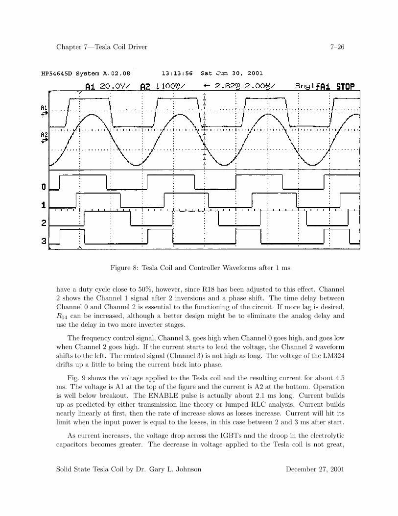
Fig. 8 shows the same waveforms after 1 ms of operation (except for Channel 4, which isno longer of interest to us). The voltage is a square wave with relatively slow transitions fromone rail to the other. The current is an almost perfect sine wave. If the voltage makes morerapid transitions from one rail to the other, switching noise will appear on the current. Forthis particular case, the current is lagging the voltage by about 7o and the duty cycle of signalon Channel 3 is about 28%, both values in a quite acceptable range.
The gate pulses from the 34066 have a duty cycle less than 50% because of the dead band.The inverted gate pulses in Channel 0 therefore has a duty cycle greater than 50%. This is nota problem in the tuning operation. The square wave representing current, Channel 1, does
Solid State Tesla Coil by Dr. Gary L. Johnson December 27, 2001
Chapter 7—Tesla Coil Driver 7–26
Figure 8: Tesla Coil and Controller Waveforms after 1 ms
have a duty cycle close to 50%, however, since R18 has been adjusted to this effect. Channel2 shows the Channel 1 signal after 2 inversions and a phase shift. The time delay betweenChannel 0 and Channel 2 is essential to the functioning of the circuit. If more lag is desired,R14 can be increased, although a better design might be to eliminate the analog delay anduse the delay in two more inverter stages.
The frequency control signal, Channel 3, goes high when Channel 0 goes high, and goes lowwhen Channel 2 goes high. If the current starts to lead the voltage, the Channel 2 waveformshifts to the left. The control signal (Channel 3) is not high as long. The voltage of the LM324drifts up a little to bring the current back into phase.
Fig. 9 shows the voltage applied to the Tesla coil and the resulting current for about 4.5ms. The voltage is A1 at the top of the figure and the current is A2 at the bottom. Operationis well below breakout. The ENABLE pulse is actually about 2.1 ms long. Current buildsup as predicted by either transmission line theory or lumped RLC analysis. Current buildsnearly linearly at first, then the rate of increase slows as losses increase. Current will hit itslimit when the input power is equal to the losses, in this case between 2 and 3 ms after start.
As current increases, the voltage drop across the IGBTs and the droop in the electrolyticcapacitors becomes greater. The decrease in voltage applied to the Tesla coil is not great,
Solid State Tesla Coil by Dr. Gary L. Johnson December 27, 2001

Chapter 7—Tesla Coil Driver 7–27
Figure 9: Tesla Coil Voltage and Current Waveforms
but is most easily noticed when ENABLE is turned off. Energy stored in the Tesla coil hasto be dissipated somehow. Instead of power flowing from inverter to coil, it now flows in theopposite direction. Voltage is constrained by the built-in diodes of the IGBTs. Power supplycapacitors are now being charged instead of discharged. All the voltage drops in wiring andthe IGBTs reverse in sign. We therefore see a small step increase in voltage when ENABLEis removed.
After about 0.6 ms, the stored energy is no longer able to force the IGBT diodes intoforward conduction. Without a power supply affecting the circuit, we now have a classic RLCring down. Both voltage and current are decreasing exponentially. During this portion of thecycle, the IGBTs are acting as capacitors.
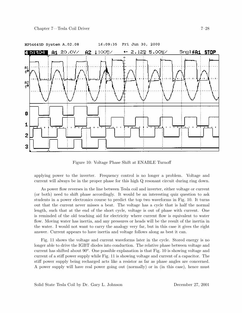
Fig. 10 shows a closeup of the waveforms when ENABLE goes low. Both outputs of the34066 go low, so Channel 0 goes high and stays there. This is the clock input to the 4013,which does not respond to constant voltage levels. The next reset pulse (Channel 2) sets the4013 output low (Channel 3), where it remains. The controller is still measuring Tesla coilcurrent, as seen by Channels 1 and 2, but is no longer controlling frequency.
Frequency is now being controlled by the Tesla coil. Instead of the controller and invertertrying to apply power to the Tesla coil at the right frequency and phase, the Tesla coil is
Solid State Tesla Coil by Dr. Gary L. Johnson December 27, 2001
Chapter 7—Tesla Coil Driver 7–28
Figure 10: Voltage Phase Shift at ENABLE Turnoff
applying power to the inverter. Frequency control is no longer a problem. Voltage andcurrent will always be in the proper phase for this high Q resonant circuit during ring down.
As power flow reverses in the line between Tesla coil and inverter, either voltage or current(or both) need to shift phase accordingly. It would be an interesting quiz question to askstudents in a power electronics course to predict the top two waveforms in Fig. 10. It turnsout that the current never misses a beat. The voltage has a cycle that is half the normallength, such that at the end of the short cycle, voltage is out of phase with current. Oneis reminded of the old teaching aid for electricity where current flow is equivalent to waterflow. Moving water has inertia, and any pressures or heads will be the result of the inertia inthe water. I would not want to carry the analogy very far, but in this case it gives the rightanswer. Current appears to have inertia and voltage follows along as best it can.
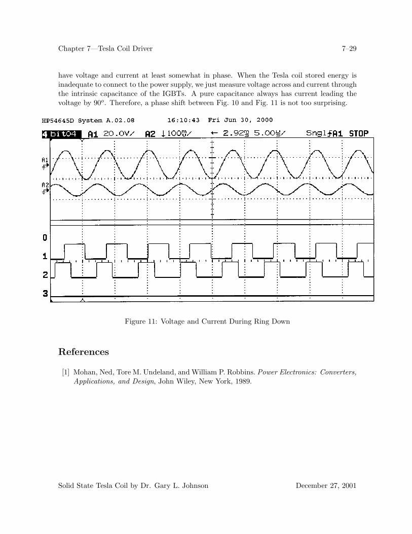
Fig. 11 shows the voltage and current waveforms later in the cycle. Stored energy is nolonger able to drive the IGBT diodes into conduction. The relative phase between voltage andcurrent has shifted about 90o. One possible explanation is that Fig. 10 is showing voltage andcurrent of a stiff power supply while Fig. 11 is showing voltage and current of a capacitor. Thestiff power supply being recharged acts like a resistor as far as phase angles are concerned.A power supply will have real power going out (normally) or in (in this case), hence must
Solid State Tesla Coil by Dr. Gary L. Johnson December 27, 2001
Chapter 7—Tesla Coil Driver 7–29
have voltage and current at least somewhat in phase. When the Tesla coil stored energy isinadequate to connect to the power supply, we just measure voltage across and current throughthe intrinsic capacitance of the IGBTs. A pure capacitance always has current leading thevoltage by 90o. Therefore, a phase shift between Fig. 10 and Fig. 11 is not too surprising.
Figure 11: Voltage and Current During Ring Down
References
[1] Mohan, Ned, Tore M. Undeland, and William P. Robbins. Power Electronics: Converters,Applications, and Design, John Wiley, New York, 1989.
Solid State Tesla Coil by Dr. Gary L. Johnson December 27, 2001