test and characterization methodologies for advanced
TRANSCRIPT

HAL Id: tel-01808874https://tel.archives-ouvertes.fr/tel-01808874
Submitted on 6 Jun 2018
HAL is a multi-disciplinary open accessarchive for the deposit and dissemination of sci-entific research documents, whether they are pub-lished or not. The documents may come fromteaching and research institutions in France orabroad, or from public or private research centers.
L’archive ouverte pluridisciplinaire HAL, estdestinée au dépôt et à la diffusion de documentsscientifiques de niveau recherche, publiés ou non,émanant des établissements d’enseignement et derecherche français ou étrangers, des laboratoirespublics ou privés.
Test and characterization methodologies for advancedtechnology nodes
Darayus Adil Patel
To cite this version:Darayus Adil Patel. Test and characterization methodologies for advanced technology nodes. Elec-tronics. Université Montpellier, 2016. English. �NNT : 2016MONTT285�. �tel-01808874�

Délivré par Université de Montpellier
Préparée au sein de l’école doctorale I2S
Et de l’unité de recherche LIRMM
Spécialité : SYAM
Présentée par DARAYUS ADIL PATEL
Soutenue le 5 Juillet 2016 devant le jury composé de
M. Daniel CHILLET Professeur, Université de
Rennes
Président du Jury /
Rapporteur
M. Salvador MIR Directeur de Recherche
CNRS, TIMA
Rapporteur
Mme. Sylvie NAUDET Team Leader,
STMicroelectronics
Examinateur
M. Alberto BOSIO MCF HDR, Université de
Montpellier
Examinateur
M. Patrick GIRARD Directeur de Recherche
CNRS, LIRMM
Directeur de Thèse
M. Arnaud VIRAZEL MCF HDR, Université de
Montpellier
co-Directeur de
Thèse
Mme. Béatrice PRADARELLI PAST, Université de
Montpellier
Membre Invitée
TEST AND CHARACTERIZATION
METHODOLOGIES FOR ADVANCED
TECHNOLOGY NODES


TEST AND CHARACTERIZATION
METHODOLOGIES FOR ADVANCED
TECHNOLOGY NODES
Presented by
Darayus Adil Patel
STMicroelectronics
Laboratoire d'Informatique, de Robotique et de Microélectronique de Montpellier
Université de Montpellier
This dissertation is submitted for the degree of Doctor of Philosophy
July 2016


Dedicated to my Beloved Parents
and
The Digital Test Team at ST Crolles


i
ABSTRACT
The introduction of nanometer technologies, has allowed the semiconductor
industry to create nanoscale devices in combination with gigascale complexity.
However, new technologies bring with them new challenges. In the era of large systems
embedded in a single System-On-Chip and fabricated in continuously shrinking
technologies, it is important to test and ensure fault-free operation of the whole system.
The cost involved in semiconductor test has been steadily growing and testing
techniques for integrated circuits are today facing many exciting and complex
challenges. Although important advances have been made, existing test solutions are
still unable to exhaustively cover all types of defects in advanced technology nodes.
Consequently, innovative solutions are required to cope with new failure mechanisms
under the constraints of higher density and complexity, cost and time to market
pressure, product quality level and usage of low cost test equipment.
The work of this thesis is focused on the development of silicon test and
characterization methodologies that aid in the accurate detection and resolution of issues
that may arise due to variability, manufacturing defects, wear-out or interference. A
wide spectrum of these challenges has been addressed from a test perspective to ensure
that the availability of effective test solutions does not become a bottleneck in the path
towards further scaling. Additionally the advances and innovations introduced in the
myriad domains of electronic design, reliability management, manufacturing process
improvements etc. that call for the development of advanced, modular and agile test
methodologies have been effectively covered within the scope of this work.
This manuscript presents the significant contributions made for enabling
resolution of state of the art industrial test challenges via the design and implementation
of novel test strategies (targeting the 28nm FDSOI technology node) for:
· Detection & diagnosis of timing faults in standard cells.
· Analysis of Setup and Hold margins within silicon.
· Verification & reliability analysis of innovative test structures.
· Analysis of on-chip self heating.
· Enabling characterization and performance evaluation of high speed digital IPs.

ii

iii
ACKNOWLEDGEMENTS
“If I have seen further than others,
it is by standing upon the shoulders of giants.”
Issac Newton
First and foremost, I would begin by thanking my Lord, the Almighty, for
holding my hand and showing the path ahead throughout the course of my thesis. Only
due to His countless gifts of sense, intellect, patience, health, family and many more,
could I complete this task. Thank you for the strength you have given me and all the
wonderful people around me who made the past three years truly meaningful.
During my time at STMicroelectronics, I was extremely fortunate to have had
the opportunity to learn and grow under the tutelage of my super amazing ‘Maman’, Dr.
Sylvie Naudet during the development of this work. I would like to gratefully and
sincerely thank Sylvie for her care, understanding, patience and most importantly
friendship during the course of my thesis from inception to completion. Despite her
busy schedule, Maman always kept a watchful eye over me and provided me with her
invaluable guidance whenever needed. To synthesize, I consider myself truly privileged
to have had this opportunity to grow my intellectual prowess, sharpen my critical
thinking and understand the subtle nuances of the game of life under her umbrella.
I am very grateful to my Professors Patrick Girard, Arnaud Virazel & Alberto
Bosio for their guidance, support and regular feedback throughout the course of my
thesis. Also for their thought-provoking ideas and helpful criticism in improving the
quality of this manuscript and other publications. Working at LIRMM under their
supervision, helped me to understand and better appreciate the academic essence of any
project. I am thankful for their time, efforts and constant interaction all along. Their
invaluable advises helped keeping my research well directed while maintaining my
autonomy.
Perhaps I owe my largest quantum of gratitude to the truly awesome team that
I was lucky to be part of at ST Crolles. Thank you Daniel Noblet for being the huge
pillar of strength that you have been for me all throughout and the ginormous force of
positivity that you are. Thank you Fabien for being a great Mentor and friend. While
learning from you I have always been inspired by your attitude, zeal and enthusiasm

iv
towards any given task. Thank you Damien Croain & Daniel Caspar for always being
there to shine light upon any technical darkness that befell me. Your mere presence
gave me the confidence that the solution to any problem could be mined out of your
mountains of knowledge. Merci beacoup my ‘Queen’ Françoise for your camaraderie
and royal influence. Many thanks to David Meyer & David Bonciani for being the great
friends that you are to me. I shall always greatly appreciate and fondly remember all
your support and help. Thank you Julien Berger for always being accommodating and
helpful. Thank you Robert ‘Bob’ Seilles for teaching me among many things that there
is a great deal more to life than just work. Thank you Loïc for always being Good.
Being part of such a wonderful team greatly accelerated my learning curve and made
life a joyful journey.
A special word of thanks goes to Deepak Kumar Arora & Kapil Juneja at ST
Noida. It was an enriching experience working with them as I benefited from their
clarity of thought and lucidity in explanation. Despite their hectic workloads they were
always available to have discussions and help me solve my doubts. I would also like to
acknowledge all the other people with whom I had the pleasure and privilege of
collaborating with. They are Abhishek Jain, Rajesh Kumar Immadi, Sujatha Balaraman,
Philippe Brahic, Sylvain Clerc, Fady Abouzeid, Franck Gardik, Jeff Nowakowski, Guy
Bossan, Shahabuddin Qureshi, Fabrice Carite, Manoubi Bourabei, Gilles Lievre, Dennis
Roche, Vincent Huard and Robin Wilson.
I would also like to express my gratitude to two of my most cherished friends
Giulio & Giulio with whom I shared the path during these last three years. Words are
not enough to describe them, they are really extraordinary. Thank you for the great
support in the moments when I needed help, for all the great time that we have spent
together and most of all for your friendship. Also a big thank you to Anu Asokan, Imran
Wali, Aymen Touati, Alejandro Nocua & Amit Karel at LIRMM for their warm
friendships and companionship.
And at last, but certainly not the least, thanks to my parents who have never
lost their faith in me and have always supported me in every decision I took, no matter
how far away from home it has taken me. Their constant support and strength has aided
and encouraged me throughout this endeavor. I shall forever remain indebted for your
love and sacrifice.
Darayus Adil Patel

v
TABLE OF CONTENTS
ABSTRACT ..................................................................................................................... I
ACKNOWLEDGEMENTS ......................................................................................... III
TABLE OF CONTENTS ............................................................................................... V
LIST OF FIGURES ..................................................................................................... IX
LIST OF TABLES .................................................................................................... XIII
LIST OF ABBREVIATIONS .................................................................................... XV
INTRODUCTION ........................................................................................................... 1
1 CONTEXT AND THESIS OBJECTIVES ................................................................ 5
1.1 SEMICONDUCTOR TECHNOLOGY EVOLUTION ............................................ 6
1.2 CHALLENGES IN ADVANCED TECHNOLOGY NODES ................................... 6
1.2.1 Variability .......................................................................................... 7
1.2.2 Manufacturing Defects ...................................................................... 8
1.2.3 Wear-out ............................................................................................ 8
1.2.4 Interference ........................................................................................ 9
1.3 FDSOI TECHNOLOGY NODE ...................................................................... 9
1.4 TESTING OVERVIEW ................................................................................. 10
1.4.1 Characterization Test ....................................................................... 11
1.4.2 Production Test ................................................................................ 12
1.4.3 Burn-in Test ..................................................................................... 12
1.4.4 Incoming Inspection ........................................................................ 13
1.5 RESEARCH OBJECTIVES ........................................................................... 13
2 AN EFFECTIVE POWER-AWARE AT-SPEED TEST METHODOLOGY FOR
IP QUALIFICATION AND CHARACTERIZATION ............................................. 17
2.1 INTRODUCTION ........................................................................................ 18
2.2 BACKGROUND AND MOTIVATIONS........................................................... 19
2.3 CIRCUIT DESIGN ARCHITECTURE AND IMPLEMENTATION ........................ 22
2.4 TEST METHODOLOGY .............................................................................. 25
2.4.1 Test Patterns..................................................................................... 25

vi
2.4.2 Test Flow ......................................................................................... 28
2.5 EVALUATION OF THE PROPOSED TEST METHODOLOGY ............................ 30
2.5.1 Memory and Runtime Evaluation .................................................... 30
2.5.2 Peak Power Analysis ....................................................................... 31
2.6 RESULTS AND ANALYSIS OF FMAX AND VMIN CHARACTERIZATIONS ...... 32
2.7 SUMMARY ................................................................................................ 36
3 ANALYSIS OF SETUP AND HOLD MARGINS INSIDE SILICON FOR
ADVANCED TECHNOLOGY NODES ..................................................................... 39
3.1 INTRODUCTION ........................................................................................ 40
3.2 STATE OF THE ART ................................................................................... 41
3.3 BASIC CONCEPTS, MEASUREMENT CIRCUIT AND METHODOLOGY ........... 42
3.4 TEST METHODOLOGY .............................................................................. 44
3.5 RESULTS AND ANALYSIS.......................................................................... 45
3.6 SUMMARY ................................................................................................ 52
4 ADAPTIVE WEAROUT MANAGEMENT WITH IN-SITU AGING
MONITORS .................................................................................................................. 53
4.1 INTRODUCTION ........................................................................................ 54
4.2 STATE OF THE ART ................................................................................... 56
4.3 MONITORING SYSTEM – DESIGN PERSPECTIVES ...................................... 58
4.4 RESULTS AND ANALYSIS.......................................................................... 62
4.4.1 In-Situ Monitors .............................................................................. 62
4.4.2 Adaptive Wearout Management ...................................................... 64
4.4.3 Power Savings ................................................................................. 67
4.5 SUMMARY ................................................................................................ 68
5 THERMAL CHARACTERIZATION USING DIGITAL SENSORS .................. 69
5.1 INTRODUCTION ........................................................................................ 70
5.2 TEST-CHIP DESIGN OVERVIEW ................................................................. 70
5.3 TEST PATTERNS ....................................................................................... 72
5.4 SELECTIVE DIGITAL CAPTURE METHODOLOGY ....................................... 74
5.5 RESULTS AND ANALYSIS.......................................................................... 78
5.5.1 Results Summary ............................................................................. 78

vii
5.5.2 Analysis and Future Directions ....................................................... 78
5.6 SUMMARY ................................................................................................ 79
6 SIMULATION AND SILICON VERIFICATION OF ADAPTIVE VOLTAGE
SCALING ...................................................................................................................... 81
6.1 INTRODUCTION ........................................................................................ 82
6.2 REFERENCE DESIGN ................................................................................. 84
6.3 AVS SIMULATION METHODOLOGY ......................................................... 87
6.4 SILICON CHARACTERIZATION METHODOLOGY ........................................ 90
6.5 RESULTS & ANALYSIS ............................................................................. 94
6.6 SUMMARY ................................................................................................ 97
7 DESIGN AND PERFORMANCE PARAMETERS OF AN ULTRA-LOW
VOLTAGE PROCESSOR ........................................................................................... 99
7.1 INTRODUCTION ...................................................................................... 100
7.2 DESIGN AND FABRICATION PLATFORM .................................................. 100
7.2.1 Technology .................................................................................... 100
7.2.2 Standard Cells ................................................................................ 102
7.2.3 Memories ....................................................................................... 103
7.3 DESIGN ARCHITECTURE AND IMPLEMENTATION .................................... 104
7.4 TEST METHODOLOGY ............................................................................ 105
7.5 RESULTS AND ANALYSIS ........................................................................ 106
7.5.1 Electrical Performance................................................................... 106
7.5.2 Cache Impact on Energy ................................................................ 107
7.6 SUMMARY .............................................................................................. 108
8 CONCLUSION AND FUTURE PERSPECTIVES .............................................. 109
8.1 THESIS SUMMARY .................................................................................. 110
8.2 FUTURE WORKS ..................................................................................... 112
SCIENTIFIC CONTRIBUTIONS ............................................................................ 113
REFERENCES ............................................................................................................ 115

viii

ix
LIST OF FIGURES
FIGURE 1.1: EFFECTS OF SCALING WITH SUCCESSIVE TECHNOLOGY NODES ....................... 7
FIGURE 1.2: SCHEMATIC LAYOUT OF BULK AND FDSOI TRANSISTORS ............................. 9
FIGURE 1.3: BASIC TESTING APPROACH ............................................................................ 10
FIGURE 1.4: BATHTUB CURVE SHOWING THE RATE OF FAILURE OF INTEGRATED CIRCUITS
AT DIFFERENT PHASES OF LIFE .................................................................................. 12
FIGURE 2.1: BASIC STRUCTURE OF A TILE ........................................................................ 22
FIGURE 2.2: ILLUSTRATION OF INSTANCE INTERFACING WITH CONTROLLING CIRCUITRY 23
FIGURE 2.3: ON-CHIP CLOCK CONTROLLER .................................................................... 24
FIGURE 2.4: IP QUALIFICATION BLOCK ........................................................................... 24
FIGURE 2.5: FLOORPLAN OF THE TEST-CHIP, INSTANCE & TILE ....................................... 24
FIGURE 2.6: AT-SPEED TIMING DIAGRAM FOR A TILE ..................................................... 26
FIGURE 2.7: OCC CLOCKING SCHEME – (A) WITHOUT PEAK POWER AWARE APPROACH (B)
WITH PEAK POWER AWARE APPROACH ..................................................................... 27
FIGURE 2.8: TEST FLOWCHART ........................................................................................ 28
FIGURE 2.9: COMPARISON BETWEEN AT-SPEED FUNCTION AND AT-SPEED ATPG
PATTERNS ................................................................................................................ 30
FIGURE 2.10: REPRESENTATIVE GRAPH OF THE FIRST FAIL FREQUENCY DISTRIBUTION .. 32
FIGURE 2.11: CAD V/S SILICON COMPARISON ACROSS MULTIPLE PVT POINTS .............. 34
FIGURE 2.12: GRAPHS OF FAILING CYCLES V/S. FREQUENCY AND VOLTAGE ................... 35
FIGURE 3.1: SIGN-OFF CLOCK DATA DE-RATES ............................................................... 42
FIGURE 3.2: CLOCK DATA DE-RATE: BASIC DIAGRAM ................................................... 43
FIGURE 3.3: TIMING DIAGRAMS FOR HOLD RISE/FALL AND SETUP RISE/FALL VIOLATIONS
................................................................................................................................. 44
FIGURE 3.4: 28NM FDSOI TEST-CHIP WITH THE CDD BLOCK EMBEDDED AT 7 DIFFERENT
LOCATIONS ............................................................................................................... 44
FIGURE 3.5: CLOCK DATA DE-RATE: EXTRA MARGIN FOR HOLD IN SILICON .................. 46

x
FIGURE 3.6: CLOCK DATA DE-RATE: EXTRA MARGIN FOR SETUP IN SILICON ................. 46
FIGURE3.7: HOLD EXTRA MARGIN WAVEFORMS FOR CAPTURE ..................................... 47
FIGURE 3.8: SETUP EXTRA MARGIN WAVEFORMS FOR CAPTURE ................................... 47
FIGURE 3.9: NORMALIZED HOLD RISE EXTRA MARGIN ON SILICON DEPICTING WITHIN
DIE VARIATIONS & CONSTITUENT COMPONENTS ..................................................... 49
FIGURE 3.10: NORMALIZED HOLD FALL EXTRA MARGIN ON SILICON DEPICTING WITHIN
DIE VARIATIONS & CONSTITUENT COMPONENTS ..................................................... 49
FIGURE 3.11: NORMALIZED SETUP RISE EXTRA MARGIN ON SILICON DEPICTING WITHIN
DIE VARIATIONS & CONSTITUENT COMPONENTS .................................................... 50
FIGURE 3.12: NORMALIZED SETUP FALL EXTRA MARGIN ON SILICON DEPICTING WITHIN
DIE VARIATIONS & CONSTITUENT COMPONENTS ..................................................... 50
FIGURE 4.1: DIFFERENT VOLTAGE MARGINS IN ADDITION TO THE NOMINAL MINIMUM
VOLTAGE .................................................................................................................. 54
FIGURE 4.2: DIFFERENT IN-SITU DELAY MONITOR SCHEMATICS ....................................... 56
FIGURE 4.3: PRE-ERROR MONITOR SCHEMATIC ................................................................ 58
FIGURE 4.4: TIMING DIAGRAM FOR PRE-ERROR MONITOR ................................................ 59
FIGURE 4.5: PATH DELAY HISTOGRAM FOR BCH IP AT DIFFERENT CONDITIONS OF
VOLTAGE & PROCESS ............................................................................................... 60
FIGURE 4.6: EXPERIMENTAL TIMING DIAGRAM SHOWING PRE-ERROR FLAGS BEHAVIOR
WITH LOWERING VOLTAGE ....................................................................................... 62
FIGURE 4.7: EXPERIMENTAL WARNING FLAG/BCH1 AUTOTEST MAXIMUM FREQUENCIES
FOR VARIOUS PVTA CONDITIONS ............................................................................ 63
FIGURE 4.8: ADAPTIVE VOLTAGE MANAGEMENT FLOWCHART ....................................... 64
FIGURE 4.9: ADAPTIVE WEAROUT MANAGEMENT (A) WITHOUT CONSIDERING AGING
EFFECTS AND (B) WITH CONSIDERING AGING EFFECTS ............................................. 65
FIGURE 4.10: DETECTION WINDOW EVOLUTION WITH STRESS TIME ................................. 66
FIGURE 4.11: MONITORING SYSTEM FAILURE RATE AND POWER REDUCTION FOR VARIOUS
DVFS OPERATING CONDITIONS ............................................................................... 67
FIGURE 4.12: TOTAL POWER SAVINGS WITH RESPECT TO STATIC VOLTAGE MARGIN AT
DIFFERENT TEMPERATURES ...................................................................................... 67

xi
FIGURE 5.1: FLOOR PLAN AND OVERVIEW OF TEST-CHIP USED FOR THERMAL
CHARACTERIZATION ................................................................................................. 71
FIGURE 5.2: PATTERN FOR STATIC SELF HEATING MEASUREMENTS ................................ 72
FIGURE 5.3: PATTERN FOR DYNAMIC SELF HEATING MEASUREMENTS ........................... 72
FIGURE 5.4: PLL AND THS CLOCK WAVEFORMS ............................................................ 74
FIGURE 5.5: MEMORY MANAGEMENT DURING DIGITAL CAPTURE [100] .......................... 74
FIGURE 5.6: SMARTEST MEMORY OVERFLOW MESSAGE ................................................ 75
FIGURE 5.7: SELECTIVE DIGITAL CAPTURE WAVETABLE ................................................ 76
FIGURE 5.8: EXAMPLE OF A DIGITAL CAPTURE VARIABLE WITH ASSOCIATED PARAMETERS
[100] ........................................................................................................................ 77
FIGURE 5.9: THERMAL CHARACTERIZATION RESULTS FOR STATIC & DYNAMIC
CONDITIONS ............................................................................................................. 78
FIGURE 6.1: BASIC REPRESENTATION OF POWER SAVINGS THROUGH ADAPTIVE VOLTAGE
SCALING .................................................................................................................. 83
FIGURE 6.2: APIP BASIC REPRESENTATION ..................................................................... 84
FIGURE 6.3: GROUPPMM BLOCK DIAGRAM ....................................................................... 85
FIGURE 6.4: FREQGEN & APIP INTERFACING ............................................................... 86
FIGURE 6.5: COMPUTATION EFFORT FOR FULL PVT SIMULATION USING FAST SPICE ....... 87
FIGURE 6.6: SIMULATION FLOWS BASED ON CUSTOMSIM & VCS AMS .......................... 88
FIGURE 6.7: SIMULATION METHODOLOGY OVERVIEW AND RESULTING RUN-TIME
IMPROVEMENT ......................................................................................................... 89
FIGURE 6.8: FLOWCHART FOR APIP FMAX CHARACTERIZATION ..................................... 91
FIGURE 6.9: FLOWCHART FOR APIP VMIN CHARACTERIZATION ..................................... 93
FIGURE 6.10: NORMALIZED SIMULATION V/S SILICON FMAX COMPARISON AT 125°C ..... 95
FIGURE 6.11: NORMALIZED SIMULATION V/S SILICON LEAKAGE CURRENT COMPARISON
AT 125°C ................................................................................................................. 95
FIGURE 6.12: NORMALIZED SIMULATION V/S SILICON DYNAMIC_POWER/MHZ
COMPARISON AT 125°C ........................................................................................... 96

xii
FIGURE 6.13: NORMALIZED SILICON RESULTS FOR POWER SAVING THROUGH AVS AT 30°C
................................................................................................................................. 96
FIGURE 6.14: NORMALIZED SILICON RESULTS FOR DYNAMIC POWER SAVING THROUGH
AVS FOR FF CORNER CHIP AT 30°C ......................................................................... 97
FIGURE 7.1: FDSOI WELL ARCHITECTURES [104] ........................................................ 101
FIGURE 7.2: STATIC CURRENT VS. FREQUENCY TREND FROM 0.5 TO 1.3V OF VDD [104] 101
FIGURE 7.3: QUASI-FO4 CRITICAL PATH ....................................................................... 102
FIGURE 7.4: POLY BIAS CELLS LEAKAGE VS QUASI-FO4 CRITICAL PATH FREQUENCY ... 102
FIGURE 7.5: 10 TRANSISTOR ULV BITCELL ................................................................... 103
FIGURE 7.6: COMPARISON OF LEAKAGE BETWEEN ULV 10T DUAL WELL (DW) AND
SINGLE WELL (SW) BITCELLS ............................................................................... 104
FIGURE 7.7: SPARC V8 32B LEON3 MICROPROCESSOR SYSTEM & FDSOI 28NM RETICLE
PICTURE ................................................................................................................. 104
FIGURE 7.8: AVERAGE MICROPROCESSOR MINIMUM VOLTAGE EXTRACTED AT 1MHZ ... 106

xiii
LIST OF TABLES
TABLE 2.1: COMPARISON OF PEAK POWER AWARE AND PEAK POWER UNAWARE
APPROACHES ............................................................................................................ 31
TABLE 2.2: NORMALIZED PROCESS VARIATION VALUES ACROSS PVT POINTS ................ 33
TABLE 2.3: NORMALIZED PERCENTAGE OF WITHIN DIE VARIATION WITH RESPECT TO
PROCESS CORNERS................................................................................................... 33
TABLE 2.4: NORMALIZED PERCENTAGE OF WITHIN DIE VARIATION WITH RESPECT TO
VOLTAGE ................................................................................................................. 34
TABLE 2.5: NORMALIZED PERCENTAGE OF WITHIN DIE VARIATION WITH RESPECT TO
TEMPERATURE ......................................................................................................... 34
TABLE 2.6: NORMALIZED CAD AND SILICON SPREAD VALUES ACROSS PVT POINTS ...... 36
TABLE 3.1: CLOCK & DATA DELAY POSITIVE DIRECTIONS IN THE GRAPH ........................ 48
TABLE 4.1: IMPLEMENTATION RESULTS OF BCH IP WITH IN-SITU MONITORS .................. 61
TABLE 7.1: MICROPROCESSOR PERFORMANCE COMPARISON ........................................ 106
TABLE 7.2: COMPARISON OF EXECUTION ENERGY WITH AND WITHOUT CACHE ACTIVATION
............................................................................................................................... 107

xiv

xv
LIST OF ABBREVIATIONS
ABB Adaptive Body Bias
APIP Area and Power IP
ASIC Application Specific Integrated Circuit
ATE Automatic Test Equipment
ATPG Automatic Test Pattern Generation
AVM Adaptive Voltage Management
AVS Adaptive Voltage Scaling
AWM Adaptive Wearout Management
BCH Bose Ray-Choudhary and Hocquenghem
BOX Buried Oxide
CAD Computer Aided Design
CDD Clock Data Derate
CMOS Complementary Metal Oxide Semiconductor
CPR Critical Path Replica
CUT Circuit Under Test
DFT Design For Test
DVFS Dynamic Voltage and Frequency Scaling
FDSOI Fully Depleted Silicon On Insulator
FMAX Maximum Frequency
FMIN Minimum Frequency
IC Integrated Circuit
IOT Internet Of Things
IP Intellectual Property
ISM In-Situ Monitor

xvi
ITRS International Technology Roadmap for Semiconductors
LOC Launch Off Capture
LOS Launch Off Shift
MTF Mean Time to Failure
PRBS Pseudo Random Binary Sequence
PV Process Variation
PVT Process Voltage Temperature
PVTA Process Voltage Temperature Aging
SE Scan Enable
SM Sequencer Memory
SOC System On Chip
SPARC Scalable Processor Architecture
STA Static Timing Analysis
UTBB Ultra Thin Body and Buried Oxide
VLSI Very Large Scale Integration
VM Vector Memory
VMAX Maximum Voltage
VMIN Minimum Voltage

1
INTRODUCTION
“Nearly all men can stand adversity,
but if you want to test a man's character, give him power.”
Abraham Lincoln
The ever-increasing advances in semiconductor technology evolution continue
to open new avenues for research in the domains of digital circuit design and test.
Designing and manufacturing smaller, faster, cheaper and low-power devices are some
of the main challenges for the semiconductor industry. The incessant increase in density
and the corresponding decrease in feature sizes of Integrated Circuits as evinced by
Moore’s Law [1] have been a driving force in the progress of the industry for the past
few decades. However, scaling of CMOS structures into the nanometer domain has
posed new challenges to the physical design and reliability of circuits. The reasons for
this are manifold [2, 22-24]. Firstly, manufacturing structures much smaller than the
wavelength of light used in modern lithography are difficult to fabricate and can be
practically done only with certain coarse limits. Similarly, it is difficult to control the
doping concentration for transistors in the nanometer range. Further, the structures are
located closer to each other with every technology node, resulting in even the smallest
of impurities or metal silvers being able to create shorts or other defects. Lastly, as the
number of transistors, wires, contacts and vias on a single chip increase, the probability
of one or more of them being faulty increases. These limitations have resulted in
increasing the probability of defects in advanced technology nodes.
A circuit defect may lead to a fault causing an error that can result in a system
failure. Manufacturing defects are physical defects introduced during manufacturing
that cause the circuit to fail to function properly. The diversity of defects makes it
difficult to generate meaningful tests maximizing the defect coverage. Fault models
which are gate-level representation of physical defects are necessary for generating and
evaluating a set of test patterns. Generally, a good fault model should accurately reflect
the behavior of the physical defects and should be computationally efficient in terms of
the time required for fault simulation and test generation. Many fault models have been
proposed, but unfortunately, no single fault model accurately reflects the behavior of all

2
possible defects that can occur. As a result, a combination of different fault models is
often used in the generation and evaluation of test patterns. Some well-known and
commonly used fault models for modern VLSI test, developed to describe different
kinds of physical defects, include the stuck-at, bridging and delay fault models [19].
As many faults are not visible at the design phase, they can only be handled by
discarding faulty chips after manufacturing and testing them. Since the faults become
visible only post-fabrication, circuits need to be tested with patterns that can detect the
presence of any defects. This in turn necessitates the need for having effective test
architectures and methodologies for efficiently capturing all modelled faults while
maintaining ease of application. Different test methodologies like parametric,
functional, structural and delay testing are combined together to maximize the fault
detection. Parametric testing is typically used to check the electrical properties of the
device and can be used to characterize any potential systematic issues with the process
node. These tests may not check any functionality of the device but can find gross
shorts, opens, leakage issues, or current drive problems. Functional testing is commonly
used for design verification to check if the output responses are inline with expected
values according to design specifications. However it is considered time consuming and
expensive due to the exhaustive nature of applying test patterns to cover each known
reachable functional state. Structural tests deal with observing the state of internal
signals at the primary outputs of a circuit. Unlike functional testing, structural tests do
not require enumeration of all functional states to test the design, so test volumes are not
as large. Delay tests are used to detect the presence of very slow-to-rise or very slow-to-
fall switching transitions and verify that a design operates correctly at the specified
clock speed.
The importance of testing cannot be overstated as it is required at different
stages of the semiconductor lifecycle from the qualification of new technology nodes to
diagnosis of in-field failures. The optimal test solution for any circuit must take into
account a wide variety of different factors like fault coverage, test cost and time,
capability of available test equipment, reliability requirement of end-user application,
etc. Often times these different factors aren’t complementary to each other and require
intelligent trade-offs to be made on a case to case basis. This eliminates the possibility
of having a global test solution for a wide variety of circuit designs and applications.
Hence custom test solutions and methodologies are required and developed which are
specific to the circuit design and application. In this context differentiated test solutions

3
for different problems at various levels of circuit complexity ranging from simple
standard cells to complex microprocessors are presented as part of this thesis. The main
contributions are divided into six distinct chapters in this manuscript. It is pertinent to
note that the organization of the chapters follows the level of circuit complexity
involved, from basic standard cells to complex microprocessors. The content of each
chapter is briefly summarized below:
· Chapter 1 details the context and objectives of the presented research work. It
starts with a discussion on the trends in semiconductor technology scaling and
the resultant challenges that have emerged. Thereafter the Fully Depleted Silicon
On Insulator (FDSOI) technology node and basic concepts related to
semiconductor test are discussed. The final part of the chapter enumerates the
main objectives of this thesis.
· Chapter 2 presents a configurable circuit and an associated power-aware at-
speed test methodology for the purpose of qualifying basic standard cells and IP
structures to detect the presence of small delay defects. The relevant silicon
results and analysis validate the proposed power-aware test methodology for
qualification and characterization of IPs and provide deeper insights for process
improvements.
· Chapter 3 presents a design and methodology for accurate characterization of
setup and hold margins of sequential elements in silicon while taking into
account effects of Process Variations. The test results provide deeper insights
into sources of extra timing margins available on silicon. This in turn, enables
accurate guard banding by preventing optimism and reducing unnecessary
pessimism in the timing margins provided during sign-off.
· Chapter 4 shows the fundamental elements towards an Adaptive Wearout
Management (AWM) control loop for the dynamic supply voltage regulation of
digital circuits. Firstly a new generation of in-situ monitors which generate
warning flags to prevent circuit failure under nominal conditions have been
explained. A voltage management control loop to efficiently tackle all voltage
margins over a large range of DVFS operating conditions and temperatures has
been implemented. The relevant experimental silicon results related to timing
windows and power savings have been provided.

4
· Chapter 5 elucidates a methodology for thermal characterization under dynamic
workloads using embedded digital sensors. Firstly the design of the test-chip
used is explained and thereafter the test patterns and test methodology employed
are elaborated upon. In particular, the methodology required for managing high
volume of data generated during such tests is elaborated upon. Analyses of the
on-chip thermal results provide useful insights for test-chip design requirements
related to thermal measurements.
· Chapter 6 presents the full silicon level electrical characterization correlation of
the simulation done using a novel method based upon existing CAD tools and a
mixed mode approach, on a representative digital design. Thus enabling
complete Process-Voltage-Temperature (PVT) characterization on the portion of
the design for which Adaptive Voltage Scaling (AVS) is defined. The
correlation of silicon results with the ones obtained via the simulation flow
provide designers with deeper insights into the gains with AVS from within the
simulation environment.
· Chapter 7 presents the design and performance metrics of a single-supply
SPARC 32bit V8 microprocessor designed with Ultra Low Voltage (ULV)
adapted standard cells and memories, aiming at low energy operation and stand
by power. A comparative analysis with similar implementations has been
provided highlighting the performance gain and power savings that are achieved
by the presented design methodology and implementation technology. Wafer-
level tests throw light on the operating range and energy savings achieved by the
ULV adapted microprocessor.
· Chapter 8 concludes the manuscript by summarizing the results of this thesis and
presenting some future perspectives.

5
1 CONTEXT AND THESIS
OBJECTIVES
“The best way to have a good idea is to have a lot of ideas.”
Linus Pauling
6
1.1 Semiconductor Technology Evolution
Technology scaling allows realization of increasingly complex systems on a
single chip. The steady growth of the global semiconductor industry over the past few
decades has been driven by the demand for enhancing performance and functionality at
reduced cost. This growth has been primarily facilitated by the continuous evolution of
semiconductor manufacturing technology. Following the so-called Moore’s law [1], the
scale of ICs has doubled every 18 months. A simple example of this trend is the
progression from Small Scale Integration (SSI) to Very Large Scale Integration (VLSI)
devices. In the 1980s, the term VLSI was used for chips having more than 100,000
transistors and has continued to be used over time to refer to chips with millions and
now hundreds of millions of transistors. In 1986, the first megabit Random Access
Memory (RAM) contained more than 1 million transistors. Microprocessors produced
in 1994 contained more than 3 million transistors. VLSI devices with many millions of
transistors are commonly used in today’s computers and electronic appliances. This is a
direct result of the steadily decreasing dimensions, referred to as feature size, of the
transistors and interconnecting wires from tens of microns to tens of nanometers, with
current submicron technologies based on feature sizes of just a few nanometers.
Transistors are scaled in each successive technology node to increase their speed,
improve packing density, decrease their power consumption and reduce cost. The
reduction in feature size has also resulted in increased operating frequencies with
current commercially available microprocessors operating in the gigahertz range. Thus,
semiconductor technology scaling optimizes circuit performance and power
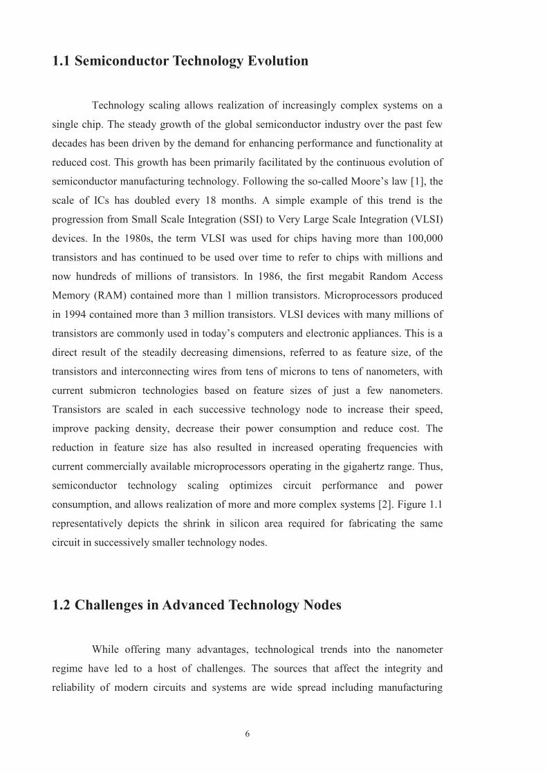
consumption, and allows realization of more and more complex systems [2]. Figure 1.1
representatively depicts the shrink in silicon area required for fabricating the same
circuit in successively smaller technology nodes.
1.2 Challenges in Advanced Technology Nodes
While offering many advantages, technological trends into the nanometer
regime have led to a host of challenges. The sources that affect the integrity and
reliability of modern circuits and systems are wide spread including manufacturing

7
Figure 1.1: Effects of scaling with successive technology nodes
process variations, manufacturing defects, wear-out and interference. In this
section we discuss some of the major issues that have emerged with technology scaling.
1.2.1 Variability
Variability of transistor characteristics due to variations in Process, Voltage
and Temperature (PVT) have always been an issue in integrated circuit design [3]. PVT
variations may prevent the circuit from achieving the required performance even in the
case of fault-free fabrication. As device scaling enters into the nano-metric regime the
effects of PVT variations are becoming excessively pronounced. Manufacturing process
variations are increased due to the lack of precise control on fabrication processes at
small-feature technologies. They cause deviation of transistor characteristics and the
resulting wide distribution leads to lower parametric yield [4]. Supply voltage scaling
brings it close to or even below the transistor threshold voltage (Vth) to achieve
significant gains in energy efficiency. Once the supply voltage is lower than Vth the
delay shows an exponential dependence on the supply voltage, and therefore the
magnitude of supply voltage shifts can have a significant impact on circuit delay [5, 6].
Scaling also gives rise to chip power densities and inadequate heat sinking cause hot
spots to appear. These fluctuations of ambient temperatures alter the timing
characteristics of circuits [7]. A conventional approach to deal with the problem of
variability is to introduce large voltage and frequency guard-bands during sign-off
which considerably impacts the power consumption and performance, cannot respond to

8
rapid environmental changes [8] and implies a sharp increase in chip cost. Effectively
dealing with variability to maintain or improve the high performance and energy
efficient systems while satisfying the required standards for reliability is becoming
increasingly challenging with the scaling of technology [9].
1.2.2 Manufacturing Defects
Semiconductor manufacturing processes may induce permanent defects in a
chip during one or more of the process steps involving implantation, etching,
deposition, cleaning and lithography due to imperfections. The device miniaturization is
making advanced technology nodes increasingly vulnerable to these manufacturing
irregularities. It is important that the testing be as thorough as possible to uncover
defective chips before they are shipped out [10]. However, according to past
microprocessor data, the die size remains relatively constant [11], whereas the number
of transistors per chip double every 2 to 3 years. This means that defect densities
continue to increase. Moreover technology scaling and increasing complexity give rise
to defects which are more subtle and difficult to detect [12, 13]. All these factors when
combined with aggressive time-to-market objectives cause test escapes and raise
reliability concerns.
1.2.3 Wear-out
Although the area scaling has had an exponential rate, the supply voltage (Vdd)
scaling has been quite slow. The two main reasons for slow Vdd scaling are to keep up
with the competitive frequency growth and to retain the basic noise immunity and cell
stability [14]. Hence the dissimilar area and supply voltage scaling rates result in high
power densities and elevated temperatures. The well-known wear-out failure
mechanisms namely Time-Dependent Dielectric Breakdown (TDDB), Electromigration
and thermal stress are all adversely affected by increase in temperature. These age-
related hard errors that appear in-field after a certain period of use are major factors
impairing the life-time reliability of modern microprocessors [15] used in data centers
and space equipment. These applications demand high throughput and better lifetime
reliability. However, these wear-out failures limit their useful lifetime and performance.

9
1.2.4 Interference
Beyond manufacturing defects and wear-out related permanent faults,
integrated systems of recent years are more susceptible to temporary effects like
transient or intermittent faults. Smaller geometries increase coupling capacitances and
as a result, cross-capacitance between wires in nanometer interconnect structures has
turned out to be the dominant component of total net capacitance. High interconnect
coupling leads to increase in circuit delay and crosstalk noise. Therefore, reducing of
interconnect coupling capacitance is an important task in the view of both circuit noise
and timing optimization. [16 - 18]
1.3 FDSOI Technology Node
Figure 1.2: Schematic layout of Bulk and FDSOI Transistors
To build better devices, the size of the transistors must be reduced while
increasing performance and reducing power consumption. FDSOI or Fully Depleted
Silicon on Insulator [38] is an advanced technology node that delivers these benefits by
building transistors that are faster, cooler and simpler. In FDSOI, the innovation lies in
inserting a thin layer of Insulator called the Buried Oxide (BOX) positioned just below
the channel and eliminating the need to add dopants to the channel, thus making it fully
depleted. Another key feature is that the silicon on oxide layer is very thin together with
the ultra thin body layer. Together this is referred to as the Ultra Thin Body and Buried
Oxide (UTBB). On the same technology node, the FDSOI transistors have a shorter
effective channel as compared to a bulk silicon transistor. This reduces the effective

10
time required by electrons to travel from the source to the drain, leading to faster
transistor. Figure 1.2 shows the schematics of Bulk and FDSOI Transistors.
As the transistor shrinks, the length of the gate is reduced and the control the
gate exercises over the channel region is also reduced thereby lowering the transistor
performance. Some unwanted leakage current flows even when the transistor is turned
off and represents a growing proportion of power consumption with each new
technology node. For FDSOI transistors, the insulator layer effectively confines the
electrons from the source to the drain thereby drastically reducing the leakage currents
from the channel to the substrate. An FDSOI chip is able to run at a lower voltage due
to the reduced margins added for process variability which also makes it cooler with
lower power consumption. To summarize, FDSOI transistors operate at lower power at
equivalent frequency as compared to their bulk counterparts.
The fabrication of all designs and their associated silicon validation results
presented within the scope of this thesis employ the 28nm FDSOI unless stated
otherwise.
1.4 Testing Overview
Figure 1.3: Basic testing approach
The reduction in feature size increases the probability that a manufacturing
defect in the IC will result in a faulty chip. A very small defect can easily result in a
faulty transistor or interconnecting wire when the feature size is less than 100 nm.

11
Furthermore, it takes only one faulty transistor or wire to make the entire chip fail to
function properly or at the required operating frequency. Yet, defects created during the
manufacturing process are unavoidable, and as a result, some number of ICs are
expected to be faulty. Therefore, testing is required to guarantee fault-free products,
regardless of whether the product is a VLSI device or an electronic system composed of
many VLSI devices. The goal of manufacturing test is to detect any defect that occurs in
the fabricated circuits. Ideally, we can differentiate faulty circuits and fault-free circuits
after the manufacturing test. Figure 1.3 illustrates the basic principle of chip testing [2]
wherein test vectors are applied to inputs of the Circuit-Under-Test (CUT), and
responses are collected and compared with expected values. If the responses match, the
circuit is considered good. Otherwise, it is considered bad. The Automatic Test
Equipment (ATE) is used to test chips. It is obvious that the test quality depends upon
the thoroughness of the test vectors. However, the test quality and test cost are
interdependent. A large number of test vectors/patterns may result in a good test quality,
but it will increase the test time and test cost at the same time. It is also necessary to test
components at various stages during the manufacturing process. Testing and diagnosis
of VLSI systems can be broadly classified into four types depending on the specific
purpose it accomplishes and the current phase of production (from fabrication to
shipment) for the circuit under test [19]. In the following subsections, four types of test
methods are briefly covered in the order they are conducted during the design and
manufacturing processes.
1.4.1 Characterization Test
Also known as design debug or verification testing, this form of testing is
performed on a new design before it is sent to production [19]. The main objective of
characterization test is to verify that the design is correct and the device will meet all
specifications. Comprehensive AC and DC measurements are made during this test
process. The requirement for thoroughness during this testing phase may often lead to
probing of internal nodes of a chip, not performed as part of any other test process.
Generally, devices are tested for the worst case because it is easier to evaluate than
average cases and devices passing this test usually work for any other conditions.

12
1.4.2 Production Test
Every fabricated chip is subjected to production tests, which are less
comprehensive than characterization tests yet they must enforce the quality
requirements by determining whether the device meets specifications. It may not be
possible to cover all possible functions and data patterns, but production tests must have
a high coverage of modelled faults. Since every device must be tested before being
packaged, test application time is of great importance. Production test should be as brief
as possible and is usually different from characterization tests.
1.4.3 Burn-in Test
Figure 1.4: Bathtub curve showing the rate of failure of integrated circuits at
different phases of life
All devices that pass production tests are not identical. When put to actual use,
some will fail very quickly whereas others will function for a long time. Burn in tests
screen for long-term reliability of devices by either continuous or periodic testing over a
period, usually under nonrated conditions. Rate of failure of integrated circuits at
different phases of life follows a bathtub curve [20] as shown in Figure 1.4. Correlation
studies show that the occurrence of potential failures can be accelerated at elevated
temperatures [21]. Two types of failures are isolated by burn-in:
1. Infant mortality failures, often caused by a combination of sensitive design and
process variation, and may be screened out by a short-term burn-in (10–30 h) in
a normal or slightly accelerated working environment, and

13
2. Freak failures, that is, devices having the same failure mechanisms as the
reliable devices, require long burn-in time (100–1000 h) in an accelerated
environment.
In practice, a manufacturer must balance economic considerations against the
device reliability. In any case, the elimination of infant mortality failures is considered
essential for most applications [19].
1.4.4 Incoming Inspection
System manufacturers perform incoming inspection (also called quality
assurance) on purchased devices before integrating them into the system. Depending
upon the context, this testing can be either similar to production testing, or more
comprehensive than production testing, or even tuned to the specific systems
application. The most important purpose of this testing, performed at the vendor site, is
to avoid placing a defective device in a system assembly where the cost of diagnosis
may far exceed the cost of incoming inspection.
The development of new technology platforms is done through the validation
of various test chips, which fulfil the fundamental requirement of determining the
silicon parameters of IP’s (functionality, timing, power, etc.) before they can be used in
a real System-on-Chip. Therefore, while qualifying new technology nodes, it is essential
to ensure that the silicon performance of test circuits is within acceptable limits.
Furthermore, accurate diagnosis and understanding of the sources of deviation from
expected behaviour is essential for improving the yield and performance of a given
technology node.
1.5 Research Objectives
The work of this thesis is focused on the development of efficient test
methodologies that aid in the accurate detection and resolution of issues that may arise
due to variability, manufacturing defects, wear-out or interference. The intent is to

14
tackle a wide spectrum of these challenges from a test perspective to ensure that the
availability of effective test solutions does not become a bottleneck in the path towards
further scaling. To this end, special emphasis is laid on capturing faults and
understanding deviation from expected behavior during the process development phase
itself. The goal is to address the great need and scope to improve and optimize existing
test structures and methodologies with regards to test time, silicon area occupied by test
structures and the ability to analyze the impact of deep submicron effects. Additionally
the aim is to develop advanced, modular and agile test methodologies that address the
advances and innovations introduced in the myriad domains of electronic design,
reliability management, manufacturing process improvements etc. The main objectives
of the thesis are briefly listed below:
· Develop a power-aware at-speed test methodology for the purpose of qualifying
basic standard cells / complex IP structures and detect the presence of small
delay defects at an early phase of technology development.
· Accurately characterize setup and hold margins of sequential elements in silicon
while taking into account effects of Process Variations. The test results should
provide deeper insights into the constituent components of extra timing margins
available on silicon. This in turn should enable accurate guard banding by
preventing optimism and reducing unnecessary pessimism in the timing margins
added during sign-off.
· Validate and characterize the functionality of a new generation of pre-error
warning monitors. Implement an Adaptive Wearout Management (AWM)
control loop for dynamic supply voltage regulation of digital circuits using the
warning flags generated by the pre-error monitors. Analyse the silicon results to
quantify the reliability benefits and power savings that are accrued from the
implemented AWM strategy.
· Develop a test methodology for thermal characterization under dynamic
workloads using embedded digital sensors. In particular, the methodology
should be capable of capturing the thermal gradient across small time intervals
and also be efficient in managing the resultant high volume of generated data.
Analyses of the on-chip thermal results should provide useful insights into
dynamic self-heating on silicon and should also show directions for future test-
chip design requirements related to thermal measurements.

15
· Implement the full silicon level electrical characterization correlation of the
simulation done using a novel method based upon existing CAD tools and a
mixed mode approach, on a representative digital design. The correlation of
silicon results with the ones obtained via the simulation flow should provide
designers with deeper insights into the gains achieved using Adaptive Voltage
Scaling from within the simulation environment.
· Evaluate the electrical performance metrics of a single-supply SPARC 32bit V8
microprocessor designed with Ultra Low Voltage (ULV) adapted standard cells
and memories, aiming at low energy operation and stand by power. Wafer-level
tests should throw light on the operating range and energy savings achieved by
the ULV adapted microprocessor. Further perform a comparative analysis with
similar implementations to understand the performance gain and power savings
that are achieved by the design methodology and implementation technology.
The above listed objectives are individually dealt with in the forthcoming chapters.

16

17
2 AN EFFECTIVE POWER-AWARE AT-SPEED TEST
METHODOLOGY FOR IP
QUALIFICATION AND
CHARACTERIZATION
“The real voyage of discovery consists
not in seeking new landscapes but in having new eyes.”
Marcel Proust
Abstract: Advanced nanometer technologies have led to a drastic increase in operational frequencies resulting in the performance of circuits becoming increasingly vulnerable to timing variations. The increasing process spread in advanced nanometer nodes poses considerable challenges in predicting post-fabrication silicon performance from timing models. Thus, there is a great need to qualify basic building structures on silicon in terms of critical parameters before they could be integrated within a complex System-on-Chip (SoC). This chapter presents a configurable circuit and an associated power-aware at-speed test methodology for the purpose of qualifying basic standard cells and complex IP structures to detect the presence of small delay defects. The circuit design has been embedded within test-chips used for the development of the 28nm Fully Depleted Silicon On Insulator (FDSOI) technology node. The relevant silicon results and analysis validate the proposed power-aware at-speed test methodology for qualification and characterization of IPs and provide deeper insights for process improvements.

18
2.1 Introduction
Consequent application of reusable components (IP: Intellectual Property) is
indispensable to enhance productivity in system design. IP qualification is a process to
measure and evaluate the specific attributes of IP cores. Its goal is to ensure that the
required quality & reliability of IP blocks is achieved and that all design constraints are
met. IP qualification offers IP providers and integrators with measurable quality
characteristics that allow making design decisions based upon quantifiable metrics of
performance and reliability [25-27]. The development of new technology platforms is
done through the silicon qualification of basic building structures/gates embedded
within test-chips, which ensure greater controllability and observability of the Circuit
Under Test (CUT). While qualifying new technology nodes, it is essential to understand
the silicon performance of CUTs and ensure that it is within acceptable limits. Test-
Chips fulfil the fundamental requirement of determining silicon parameters of IP’s
(functionality, timing, power, etc.) before they can be integrated in a real SoC design.
Having modular design architectures for test, effective test methodologies, efficient
diagnosis of defects and the ability to accurately characterize the impact of Process
Variations (PV) [28, 29] is essential to the IP Qualification process.
From a post-silicon test point of view, the physical phenomenon observed in
deep sub-micron nodes give rise to new defects and immensely complicate the task of
timing analysis and path selection for testing and grading the final chips. IC
manufacturing test is continually evolving, with an increased emphasis on at-speed
testing to maintain test quality for larger, more complex chips and new fabrication
processes. At-speed testing is crucial for ensuring product quality from the timing
performance point of view and maintaining the reliability level of chips delivered to
customers after testing. At-speed testing is now the industry norm as many timing
related defects go undetected by ATPG patterns generated using the classical stuck-at
and bridging fault models [30, 31]. Further, power consumption during test is
significantly higher than during normal functional mode [19, 32-35]. The reason is that
test patterns tend to activate switching on a large number of nodes while a typical
functional mode only activates a small portion of the design at any given time instance.
Also successive functional input vectors applied to a given circuit during system mode
have significant correlation, while the correlation between consecutive test patterns can
be very low [36]. The excessive power consumption can result in parts being damaged

19
during test, or in preventing good parts from passing test, leading to yield loss. This
necessitates the need to develop power-aware test methodologies. In order to have
proper characterization in terms of timing it becomes inevitable to evaluate the impact
of aging degradation too through burn-in tests. Stress tests such as high voltage tests and
burn-in tests are often used to perform accelerated testing in order to detect infant
moralities and screen weak parts [37]. Furthermore, accurate diagnosis of the sources of
defects & deviations from expected behaviour is essential for improving the yield and
performance of a given technology.
In this context, this chapter presents a circuit design which may be embedded
within test-chips and an effective test methodology that enables the characterization of
basic standard cells and/or complex IP structures. This helps in detecting Small Delay
Defects (SDD) at an early phase of technology development. The circuit design & test
methodology have been optimized for low power consumption & used for the
development of the 28nm FDSOI technology node [38]. The associated relevant results
and analysis provide deeper insights into the speed limitations, reliability and
defectivity of the said technology node. Furthermore, silicon results help in the
diagnosis of captured defects and in qualifying the standard cell library with respect to
multiple Process-Voltage-Temperature (PVT) configurations.
2.2 Background and Motivations
Performance verification in the presence of PV is difficult to perform because
the critical path is no longer unique. Different paths become frequency limiting in
different process corners. In advanced nanometer manufacturing, systematic delays
owing to unpredictable process changes have assumed a greater share of customer fails
than catastrophic defects [39]. Conventional ASIC design methodology uses pre-
characterized standard cells to optimize the design as per specifications. During the
process development phase it is necessary to complement pre-silicon analysis with post-
silicon timing and power characterization on fabricated devices. Characterization results
are used to identify outliers, understand the impact of PV and improve the design before
ramp and production [40]. Accurate timing characterization of standard cells as well as

20
complex IPs is required for power and performance optimization of designs which
embed them.
It has been observed that the presence of random defects can affect circuit
performance with very slow-to-rise or very slow-to-fall switching transitions [41]. Such
defects can cause an increase in the delay of paths going through circuits. A device fails
to operate at the rated speed if it contains a delay defect that creates a path delay higher
than the maximum allowed path delay [42]. The different fault models for generating
test patterns for delay defect detection are the transition delay model, the path delay
fault model and the SDD fault model. In the transition fault model [43], a gate net has a
slow-to-rise and a slow-to-fall fault associated with it while the path delay fault model
[44] targets the cumulative delay through the entire set of gates in a pre-defined path.
Moreover, the path delay fault model not only takes into account the cumulative delay
through the entire list of gates in a pre-defined path, but it can also take into account
localized delay defects. Depending on how delay faults are tested in scan design
environment, there are two transition delay fault pattern generation approaches, namely
the Launch-Off-Shift (LOS) and Launch-Off-Capture (LOC) schemes [30, 45].
Application of at-speed tests for detecting delay faults in synchronous sequential
circuits is usually done using scan-based structural tests generated by an Automatic Test
Pattern Generator (ATPG). Timing-aware ATPGs require long CPU run time for pattern
generation and fault simulation, and also result in a significantly large pattern count
[46]. In [47], a variation aware method based on statistical timing to select critical paths
for structural test is discussed wherein path delays are projected into different process
corners using their linear delay function forms. The work of [48] has explored
improving transition fault pattern quality through at-speed diagnosis to automatically
identify the failing paths and locate the root cause of failure. The premise is that
complete timing information is unavailable during ATPG and it may be possible that
some of the at-speed patterns may activate paths which are not required to meet system
speed (for e.g. non-functional paths), and these patterns may fail during production test.
Power inducing over-test occurs when fully-functional chips fail during testing
because of excessive heat and/or Power Supply Noise caused by test patterns with
excessive switching activity and is rapidly becoming one of the most serious problems
in scan testing, especially for low-power, high-speed, and deep-submicron integrated
circuits [49, 50]. This is particularly aggravated during burn-in testing which can lead to
significant power variations within the die [51]. Since power consumption increases

21
significantly with elevated temperature and voltage, the execution of burn-in tests can
be limited by the allowed power dissipation budget [52]. For scan-based tests, power is
divided into shift-power and capture-power. Shift-power is the power consumed during
the process of simultaneously serially loading the test stimulus and unloading the
previous test response whereas capture-power is the power consumed during one or
more capture clock cycles. Generally, test power problems are classified as peak power
issue which is highest permissible value of power at any given instant and average
power issue which is total distribution of power over a time period [53]. Test power
reduction can be addressed at various stages of test generation for logic circuits, by
employing low-power ATPG, low-power test compaction, low-power X-filling, and
low-power test vector ordering [54]. The most significant advantage of reducing test
power through low-power test generation is that this approach causes neither circuit
overhead nor performance degradation. Power-aware Design-for-Test (DfT) techniques
allow for controlling the power consumption and reduce the overall energy consumed
during test. Clock gating can be employed to reduce test power without impacting fault
coverage. Techniques such as segmentation, clustering and ordering of scan cells reduce
the power consumption, and improve the effectiveness of power reduction techniques
such as test planning and power-aware test generation [54]. A common method to
reduce the excess switching activity during shifting is to split the scan path into several
segments. Shifting is then done one segment after the other [55]. The segments not
currently active are not clocked and do not contribute to shift power. Staggered clocking
or skewed clocking is a technique used in low-power design where segmented parts of a
design are clocked in an alternating fashion to reduce the simultaneous switching
activity and thereby the peak power during test [56, 57].
The work of this chapter focuses on the detection of timing related defects at
the standard cell level during the process development phase. The presented power-
aware modular design structure and test methodology allow for the reduction of capture
power during at-speed tests. The proposed framework and methodology simplify the
procedure for fault diagnosis and outlier localization using functional at-speed patterns.
The associated results and analysis help in further understanding the effects of PV
across multiple corners on timing related defects and design margins.

22
2.3 Circuit Design Architecture and Implementation
Figure 2.1: Basic structure of a Tile
The primary intent of the design is to enable the qualification of basic digital
structures, gates or IPs by accurately determining their operational parameters and
characteristics at high frequencies. In terms of physical implementation, a bottom-up
approach has been used by implementing the basic building structure of the design and
then using it as a hard-macro for further implementation. This basic building structure
referred to as a Tile and is shown in Figure 2.1.
A tile consists of N different standard cells or complex IP structures between
launch and capture flops. The capture flop is referred to as the Scan Flop as it forms part
of the output scan chain. The Circuit Under Test (CUT) refers to a single standard cell /
IP as shown in Figure 2.1. CUTs embedded within a tile for the purpose of qualification
differ in terms of geometry and characteristics such as layout, orientation etc. A CUT is
activated and tested by either a rising or falling transition. A NX1 multiplexer is used to
select & observe the output of any CUT within the tile, which is then captured into the
scan flop. Scan flops of multiple tiles are stitched together to facilitate the shifting out
of the CUT’s capture response, such that it is observable on the top-level pad of the test-
chip. The excitation stimuli may be either generated on-chip or loaded externally
depending on the mode in which we are the structure is operated. For retaining
observability in case of any faults within the scan chain, redundancy has been added
using a Bypass Mux structure. Launch and capture flops as well as multiplexers
employed within the tile have higher reliability as compared to embedded CUTs i.e.
they have been qualified earlier or if the tile is used for the qualification of an entirely
new technology node, these cells employ a relatively relaxed geometrical layout. A tile

23
can be clocked dynamically by either using the slow tester clock or a fast clock
generated using an on-chip PLL.
Figure 2.2: Illustration of instance interfacing with controlling circuitry
For having a large population of tiles to help in better understanding the
properties of fabricated devices while maintaining ease of design, each tile is replicated
several times within an instance as shown in Figure 2.2. Each instance is then interfaced
with an internal on-chip data generator and an On-Chip Clocking (OCC) mechanism.
The internal data generator is a Linear Feedback Shift Register which provides rising
and falling transitions. Having an on-chip data generator provides the possibility to
easily test an instance when it is not possible to apply stimuli from top-level pads of the
test-chip. Such a requirement may be mandatory for Burn-In testing where limited
number of pins may be available on the Burn-In board due to hardware limitations of
the oven equipment.
The on-chip clock controller shown in Figure 2.3 is used to generate at-speed
clock pulses. The OCC is a complex multiplexer with synchronization circuitry, which
selects between at-speed (PLL) clock and slow clock depending on the status of the
Test_Enable signal. The length of the Clock Shift Register is easily configurable & is
programmed to generate the required number of fast clock pulses during capture mode,
i.e. Test_Enable = 0 & Test_Mode = 1. During capture, the Test_Enable signal is
latched internally at the negative edge of the Slow_Clk which enables the generation of
fast clock pulses depending on the contents of the clock shift register. The configurable
clock shift register provides flexibility to adjust the arrival time of the at-speed pulses
after the Test_Enable signal goes low. This forms the basis of the proposed architecture
for peak power reduction.

24
Figure 2.3: On-Chip Clock Controller
Figure 2.4: IP Qualification Block
Figure 2.5: Floorplan of the Test-chip, Instance & Tile

25
As shown in Figure 2.4, an instance is further replicated inside a Block with
the goal of increasing the cell population. For the test case under consideration, a single
block contains 5 instances with 100 tiles (Instances 1 - 5) and 3 instances having 50 tiles
(Instances 6 - 8). Each tile embeds within itself 128 CUTs. This leads to a population of
about 80k CUTs within a single block. However, this configuration can be easily
modified to suit specific requirements. Having multiple instances embedded within a
single test-chip allows studying the impact of within die variations on performance.
This architecture and implementation flow not only enables IP qualification but also
helps us to reuse small portion of the structure multiple times resulting in reduction of
overall development cycle of the test-chip. The modular design allows sharing resources
and increasing area utilization efficiency for different tiles and instances. The presented
circuit design is capable of being clocked in the GHz range and occupies a chip area of
1.18 mm2 when implemented in the 28nm FDSOI technology. Figure 2.5 shows the
floor-plan of the test-chip, instance and tile respectively.
2.4 Test Methodology
In this section, firstly the application of power-aware at-speed patterns
employed for testing tiles within the test-chip design have been explained with the aid
of timing diagrams. Thereafter, the test flow used for qualifying the CUTs embedded
into the test-chip is explained.
2.4.1 Test Patterns
Figure 2.6 shows the timing diagram when a tile is clocked during at-speed
test. The LOC approach is used for this implementation permitting the scan chain to
shift at low speeds and simplifying the design by eliminating the need for switching the
Scan Enable (SE) signal at high frequencies. The dynamic clock signal from the On-
chip Clock Controller is used to clock the launch flop, the CUT and the scan flops,
enabling them to be either clocked at low frequencies using the tester clock or at high
frequencies using the on-chip PLL. Initially, data coming from either the top level pads
of the test-chip or from the internal data generator is stabilized at the input of the launch
flop. The input of the launch flop toggles whenever the Test SE signal goes low, which

26
Figure 2.6: At-Speed Timing Diagram for a Tile
ensures a transition at the input of the CUT during at-speed test. Thereafter, three at-
speed pulses are provided when the SE signal is low which sequentially triggers the
output of the launch flops, CUT and scan flops. Data from the scan flop is then shifted
out at slow speeds. At-speed patterns used for testing the design may either be
developed using an ATPG tool or written using a cycle based pattern development
language. In the rest of this chapter, at-speed patterns developed using an ATPG tool are
referred to as at-speed ATPG patterns whereas those developed using a pattern
development language are referred to as at-speed functional patterns.
For increasing efficiency and reducing test time, multiple instances are tested
in parallel. From a peak power perspective, it is necessary to optimize the capture power
as the number of CUTs switching during capture is much greater than the number of
nodes switching during scan shifting. This is due to the fact that within a tile, activity is
induced on N CUTs which are tested in parallel and only a single scan flop which is
stitched across tiles to form the scan chain. Assuming a switching activity of X at any
time for each instance embedding 100 tiles, this particular implementation would result
in a total switching activity of 6.5X since a single block embeds 5 instances with 100
tiles and 3 instances with 50 tiles. Such concurrent switching as shown in Figure 2.7(a)
would cause an unacceptable spike in peak capture power. For tackling peak power
issues during capture, at-speed pulses for each instance are mutually skewed such that at
any given point in time, the capture pulses for just a single instance induce activity as
shown in Figure 2.7(b). This is achieved by setting the required length of the Clock

27
Figure 2.7: OCC clocking scheme – (a) Without peak power aware approach (b)
With peak power aware approach
Control Shift Register of the OCC during the design phase and then programming it
accordingly to provide the required skew amongst instances. This approach induces a
maximum switching of X across all instances at any point of time during capture. In
order to guarantee this clocking scheme on silicon, clock skew of zero must be ensured
at the input of each instance.

28
2.4.2 Test Flow
Figure 2.8: Test Flowchart
Steps to test the design for deriving the silicon spread and detecting any
outliers present on silicon are sequentially performed as follows (see Figure 2.8):
1. Firstly the status of an ATPG pattern generated using the Stuck-At fault model is
checked for the entire block to filter the presence of any static faults present
within the design.
2. The functionality of the reference scan chain is verified at low speeds by
ensuring that a reference pattern is well propagated.
3. The functionality of the bypass structure is verified at low speeds by ensuring
that reference data is well captured.
4. Functional scan patterns which apply a sequence of input data to the CUTs
within an instance are tested at low speed. This provides a picture of the
functional integrity of CUTs at low frequencies.

29
5. Steps 1-4 are performed at nominal operating conditions and an instance is
considered to be faulty if a failure is observed on any pattern during these steps.
Thereafter, characterization using at-speed patterns is performed by determining
the maximum frequency (Fmax) or the minimum voltage (Vmin) of operation.
Fmax Characterization: Functional at-speed scan pattern with high-frequency capture
pulses and low-frequency shift out is tested repeatedly for multiple frequencies in the
entire test frequency range. This is done by dynamically modifying the PLL frequency
programmed within the functional at-speed pattern. A step size of 10Mhz has been used
to achieve the required test granularity but may be easily adjusted to suit specific
requirements.
Vmin Characterization: Functional at-speed scan pattern with high-frequency capture
pulses and low-frequency shift out is tested repeatedly for multiple voltage points in the
entire test range. A step size of 10mV has been used to achieve the required test
granularity but may be easily adjusted to suit specific requirements.
The first failing frequency/voltage for every instance is logged to have an
insight into the speed limitation of the tile on silicon. The subsequent failures are
captured to observe the silicon spread in terms of delay. For failing
frequencies/voltages, a cycle-based failure datalog is generated for diagnosis, which
simply details the failing cycles and the output pin. Using this information, the failing
CUT, tile and instance can be easily identified as a particular failing cycle can be
accurately mapped back to the failing CUT. On a comparative basis, Vmin
characterization is faster as compared to Fmax characterization as there is no need to
dynamically modify the pattern during runtime for programming the PLL. This makes
Vmin characterization more suitable to production test where a simple change of the
input spec value is required. Also, most silicon test environments provide in-built
functions for performing a Vmin search. However, an Fmax search is more suitable for
understanding the silicon spread in terms of frequency at any given voltage point.
Silicon wafers with test-chips having our design embedded within them have been
fabricated as part of a corner lot using the 28nm FDSOI technology node. For the
purpose of investigation, wafers of the slow, typical and fast corners were tested at
multiple temperatures using the Verigy 93k automated test equipment.

30
2.5 Evaluation of the proposed Test Methodology
This section provides a comparative analysis of the different at-speed patterns
that may be used in the test methodology and highlight the benefits of the power-aware
approach.
2.5.1 Memory and Runtime Evaluation
Figure 2.9: Comparison between At-Speed Function and At-Speed ATPG Patterns
The design architecture supports at-speed testing with patterns that may either
be developed using an ATPG tool or written using a cycle based pattern development
language. Figure 2.9 graphically displays the comparison between at-speed functional
and at-speed ATPG patterns for a single instance with respect to memory requirement
and runtime. From the graph it is evident that at-speed functional patterns require about
90% less memory as compared to at-speed ATPG patterns as these patterns use an
internal Finite State Machine to generate control signals and apply stimuli to the
embedded CUTs. At-speed functional patterns are two magnitudes of order faster than
the ones generated using an ATPG tool, in terms of the number of tester cycles required
for their execution. Since a functional pattern is cycle-based, a deeper knowledge of
design interactions and activations from within the pattern is easily available. This
information is essential for programming the PLL to produce a range of frequencies
when operated at a constant input frequency. Furthermore, at-speed functional cycle-

31
based patterns simplify the diagnosis process as a failing cycle can be easily mapped
back to the faulty CUT. This is due to the fact that for at-speed functional patterns, each
particular failing cycle corresponds to a unique CUT within the design and may be
tabulated in a look-up table and does not require the design database for diagnosis as in
the case of tests performed using at-speed ATPG patterns. The process of identifying
failing CUTs with at-speed functional patterns has been automated using a script, which
reads the pattern description and Tester generated failure datalogs to isolate failing
CUTs. Both at-speed patterns i.e. functional and ATPG, provide 100% fault coverage
with the transition fault model on the targeted CUTs. The only comparative drawback
of Functional patterns is that they need to be generated manually as compared to tool
based generation for ATPG patterns and require deep knowledge regarding the
implementation details of the block.
2.5.2 Peak Power Analysis
Quality Parameter
Peak Power (W)
SS_0.6V_-40°C FF_1.3V_125°C
Power Unaware Approach 0.1516 2.0135
Power Aware Approach 0.0427 0.6021
Percentage Reduction 71.83% 70.1%
Table 2.1: Comparison of Peak Power aware and Peak Power unaware approaches
Peak power analysis results derived using Synopsys Prime Time for the IP
qualification block are presented in Table 2.1. It could be seen that under best PVT
corner for stress (SS_0.6V_-40°C), the peak power at any instant of time is low for both
power aware and unaware approaches. However for the worst stress corner
(FF_1.3V_125°C), peak power consumption with the power unaware approach is much
higher and could violate the power budget for the test-chip which would be risky for
silicon testing. Further with power-aware approach, it is found that power consumption
reduces by almost 70% across PVT corners which enable to comfortably meet the
power budget of the block.

32
2.6 Results and Analysis of Fmax and Vmin Characterizations
This section presents the results and analysis of Fmax and Vmin
characterization. It begins by showcasing the resultant impact of process variation and
further investigates process-corner, voltage and temperature as individual contributors
to variation. Thereafter the CAD vs. Silicon alignment at multiple PVT points is
studied. Finally the silicon spread with respect to frequency and voltage is analyzed.
Figure 2.10: Representative graph of the First Fail Frequency Distribution
Figure 2.10 shows a representative graph of the first fail frequency derived via
Fmax characterization across a population of dies embedded within the test-chip at a
single PVT point. Analysis of the data allows us to quickly understand the global speed
limitation across all instances within the block. The quantum of within die variation and
within wafer variation is easily discernable from the results. Within die or within wafer
variation refers to the difference between the maximum and minimum values of the first
failing frequency of instances within a die or across a wafer. Characterization for the
block was performed at various PVT points to understand the impact of process
variations across different process corners. The two metrics used to highlight these
values here are the percentage of average within die variation and the percentage of
within wafer variation. Their normalized values are listed in Table 2.2.

33
Values listed in Table 2.2 have been normalized using normalization factors
based on the absolute values at the PVT Point TT_1.0V_25°C. From a comparative
point of view, it can be seen that there is no linear correspondence between within die
and within wafer variations i.e. a higher amount of within die variations may not
PVT Configuration Normalized Percentage of Average Within Die
Variation
Normalized Percentage Within Wafer Variation
SS_0.6V_-40°C 1.053686232 2.555555556
SS_0.8V_-40°C 0.744038322 1.590268886
TT_1.0V_25°C 1 1
FF_1.3V_125°C 2.186772963 1.637221269
Table 2.2: Normalized Process variation values across PVT Points
necessarily lead to a higher amount of within wafer variations. The methodology and
analysis provides designers with accurate inputs regarding the amount of guard-banding
to take into account the effects of process variations at a given PVT point. To have a
better understanding of process, voltage and temperature as individual contributors to
variation, wafers are tested under dynamic conditions and the normalized values of
within die variation are listed in Tables 2.3, 2.4 and 2.5. Trends derived from the results
in Table 2.3 show that the variation is least for the slow process corner and most for fast
process corner. From Table 2.4 it can be seen that within die variation is directly
proportional to voltage while Table 2.5 shows that within die variation is inversely
proportional to temperature.
The derived data is also used to compare silicon results with the sign-off
estimates and, for this purpose, the instance having the median first failing frequency
across dies is selected. Figure 2.11 shows the CAD v/s Silicon comparison of the first
failing frequency across different PVT points. From the graph it can be seen that CAD
PVT Configuration Normalized Percentage of Average Within Die
Variation
SS_1V_25°C 0.922901
TT_1V_25°C 1
FF_1V_25°C 1.087106
Table 2.3: Normalized Percentage of Within Die Variation with respect to Process
Corners

34
PVT Configuration Normalized Percentage of Average Within Die
Variation
TT_0.6V_25°C 0.286596
TT_0.8V_25°C 0.656665
TT_1V_25°C 1
Table 2.4: Normalized Percentage of Within Die Variation with respect to Voltage
PVT Configuration Normalized Percentage of Average Within Die
Variation
TT_1V_-40°C 1.037410046
TT_1V_25°C 1
TT_1V_125°C 0.924126355
Table 2.5: Normalized Percentage of Within Die Variation with respect to
Temperature
Figure 2.11: CAD v/s Silicon Comparison across Multiple PVT Points
and silicon values are perfectly aligned at SS_0.6V_-40°C. It is seen that CAD data is
pessimistic at SS_0.8V_-40°C, i.e. the median first failing frequency on silicon is higher
than the one expected in CAD. Whereas at TT_1.0V_25°C & FF_1.3V_125°C the CAD
data are optimistic as compared to the silicon results. This information is vital for

35
calibrating CAD models to accurately reflect the performance on silicon and thus save
debugging time and effort.
Figure 2.12: Graphs of Failing cycles v/s. Frequency and Voltage
The failure datalogs of instances having the lowest first fail frequency are considered
for deeper analysis to locate cells with the lowest speed tolerance. Outlier cells if any
are chosen for failure analysis to isolate any design limitations or process imperfections.
Such a study is important on standard cells that are the basic building blocks of complex
SoCs, as cells having lower than anticipated speed may contribute to SDD which may
cumulatively result in timing failures. Resolution and elimination of timing defects
during the early phase of process development also helps in ramping up the yield at
faster rate. Figure 2.12 depicts graphs showing the total failing cycles as well as the
incremental failing cycles with respect to frequency & voltage for a single instance with
100 tiles, i.e. 12800 CUTs. While interpreting the graphs of Figure 2.12, it is important
to note that both rising & falling transitions cause a single cycle to fail with a functional
at-speed pattern. Hence as seen in Figure 2.12, at a constrained value of frequency /
voltage when all CUTs are failing, a total of 25600 cycle failures are recorded. Since
Fmax characterization is performed at a finer granularity as compared to Vmin
characterization, a higher number of data points are seen in the graph for the failing
cycles vs frequency. This analysis provides an insight into the window of frequency /
voltage between the first and last failing CUT of an instance and helps in better
calibrating CAD models for accurate sign-off.
Table 2.6 shows the CAD & silicon spread values across multiple PVT points
which have been normalized using normalization factors based on the absolute values at
the PVT point TT_1.0V_25°C. In order to calculate the silicon spread, the difference
between the average frequency at which the first cycle fails & the average first
frequency at which all cycles fail is considered for each PVT point. From the results it

36
can be seen that the trends for CAD and silicon data are well aligned across PVT points
and the degree of divergence between CAD & silicon can also be accurately gauged.
Understanding the silicon spread provides an accurate idea of dynamic voltage and
frequency scaling limits that may be applied for designs embedding the qualified cells.
PVT Configuration Normalized CAD
Spread
Normalized Silicon
Spread
SS_0.6V_-40°C 0.251851524 0.291666667
SS_0.8V_-40°C 0.647669182 0.833333333
TT_1.0V_25°C 1 1
FF_1.3V_125°C 1.797637065 1.45758636
Table 2.6: Normalized CAD and Silicon spread values across PVT Points
It is important to note that the normalized and comparative results provided in
this section are derived from a specific process flow of the technology under
investigation. However the design and test methodology is generic in nature and may be
deployed in test-chips across process flows and technology nodes for the purpose of
library qualification.
2.7 Summary
This chapter presents a test circuit for accurately characterizing IPs and
standard cell libraries using at-speed testing. The design supports the qualification of
basic building gates, cells and structures on silicon during the process development
phase in terms of timing before they are integrated within complex SoCs. The presented
power aware design and test methodology helps mitigate peak power issues during
capture and reduce power consumption by about 70%. The implementation allows the
use of both at-speed functional and at-speed ATPG patterns, and a comparative analysis
of both approaches in terms of memory requirement, test time etc. for this specific
design is put forth. The presented design has been tested and validated for the 28nm
FDSOI node. The results provide an insight into the impact of within die and within
wafer variation across multiple PVT points. Information regarding CAD vs. silicon
correlation derived from the test results helps to efficiently optimize CAD models and

37
determine the timing margins provided during sign-off. Fault diagnosis using the
derived silicon results helps in deeper understanding & resolution of design ambiguities
and process limitations. In the future, this block is intended to be deployed for the
assessment of even smaller technology nodes during the process development phase.

38

39
3 ANALYSIS OF SETUP AND
HOLD MARGINS INSIDE
SILICON FOR ADVANCED
TECHNOLOGY NODES
“Who looks outside, dreams; who looks inside, awakes.”
Carl Jung
Abstract: This chapter presents a design and methodology for accurate characterization of setup and hold margins in silicon while taking into account effects of Process Variations (PV). The test circuit provides deeper insights into sources of extra timing margins available on silicon. This in turn, enables accurate guard banding by preventing optimism and reducing unnecessary pessimism in the timing margins provided during sign-off. The presented design has been used for the development of the 28nm Fully Depleted Silicon On Insulator (FDSOI) node and associated relevant results and analysis have been provided.
40
3.1 Introduction
As device geometries continue to shrink in order to achieve higher integration density
and performance, the ability to control critical device parameters is becoming
increasingly difficult. With every consecutive technology node, circuit performance
becomes ever more sensitive to process variations [28] as significant variation in device
length, width and oxide thickness have been observed. The loss in performance due to
Process Variation (PV) can be equal to the gain by one full technology generation [58].
With frequencies increasing aggressively, even pico-second variations cannot be
ignored, in particular, for high speed clock design. Characterizing and managing PV is
becoming a critical issue for technology nodes in the nanometer range. Process
variations not only affect yield, but also have an impact on performance and reliability.
Timing analysis for signoff can no longer ignore PVs whose signature is observed from
foundry-to-foundry, lot-to-lot, wafer-to-wafer, within-wafer and also within-dies. In
particular, within-die variations are becoming progressively significant with each
technology node [29]. Hence, additional conservatism is added to account for these
variations, which can result in missed timings on the clock and data paths. Such margins
are added during sign-off and are referred to as De-rate in the rest of this chapter. It is
observed that simple guard banding to mitigate the effects of PV leads to increased
product development times and uncompetitive products. In addition, traditional Static
Timing Analysis (STA) methodologies are unable to cope with the large number of
permutations of process, voltage, and temperature corners created by these independent
and increasingly random sources of variation [59 - 61].
The development of new technology platforms is done through the validation of various
test chips, which fulfil the fundamental requirement of determining the silicon
parameters of IP’s (functionality, timing, power, etc.) before they can be used in a real
System-on-Chip. Therefore, while qualifying new technology nodes, it is essential to
ensure that the silicon performance of test circuits is within acceptable limits.
Furthermore, accurate diagnosis and understanding of the sources of deviation from
expected behaviour is essential for improving the yield and performance of a given
technology node.
This chapter presents a novel yet simple test circuit for accurate characterization of
Setup and Hold margins while taking into account effects of PV. The circuit consists of
a data path between launch and capture flops whose skew can be accurately controlled

41
to cause hold / setup violations. This design has been used for the development of the
28nm FDSOI [38] node and the associated relevant results and analysis provide deeper
insights into the effects of PV and the constituent components of the timing margins
observed on silicon.
3.2 State of the Art
Several methods have been proposed for enhancing yield and reliability as well as
improving timing analysis while factoring in PV. Firstly [62, 63] discuss statistical
methods for estimation and control of PV effects on circuit operation. Ring-oscillator
based measurement circuits are the most popular digital techniques for on-chip
variability control and are often used for simple and fast characterization of the AC
characteristics of digital CMOS circuits [64, 65]. However, what the frequency of a ring
oscillator tells us is how fast or slow a chip can operate and this data would need to be
further post processed to take requisite decisions for tuning performance in the presence
of variability. Post-fabrication tuning of substrate bias has been suggested in order to try
and compensate for threshold-voltage variation [66]. The study of the impact of process
and environmental variation on ASIC timing and methodologies to account for them
while modelling circuit delay and performing STA have been shown in [59, 60].
Nevertheless these methods take into account just the systemic variations while ignoring
random variations, which contribute to an increasing proportion of global variation in
deep sub-micron nodes.
In [67] a new statistical definition for setup and hold time is put forth which accounts
for PV whereas [68] motivates the fluctuation of setup time, hold time and Clock-to-Q
Delay under dynamic conditions and presents a method to cope with dynamic power
supply noise in FF timing estimation. In [69] a methodology for interdependent setup
and hold time characterization of sequential circuits has been presented. However once
again this aims at reducing pessimism in STA without taking into account PV effects on
silicon. Post-silicon skew tuning via Programmable Delay Elements, which aims at
overcoming the effects of PV by utilizing setup and hold timing tests has been shown in
[70]. A hold time failure model is defined and an approach for explicit validation of
hold time violations is shown in [71]. The work presented in this chapter takes forward

42
the State-of-the-Art by presenting a test circuit and methodology for characterizing
Setup and Hold margins on silicon and understanding the constituent components of
these margins.
3.3 Basic Concepts, Measurement Circuit and Methodology
Figure 3.1: Sign-off Clock Data De-rates
In order to ensure that designed circuits maintain functional integrity in light of process
and runtime variations, extra pessimism is added for Setup & Hold margins during
Sign-off, which are referred to as de-rates herein. As shown in Figure 3.1, in order to
safeguard against hold violations, the launch clock path is made faster and the capture
clock path is delayed after de-rating for hold checks. Similarly to prevent setup
violations, the launch clock path is made slower and the capture clock path is made
faster after de-rating. Data de-rates make the data path faster for hold & slower for setup
checks. The common clock path variations in Launch and Capture clock paths are
ignored.
A test circuit namely the Clock Data De-rate (CDD) block has been designed as a hard
macro to characterize and analyze setup and hold margins. This is done by measuring
the variation of delay in the Clock and Data paths to validate the de-rate added during
sign-off. The basic diagram of the CDD block is shown in Figure 3.2. The circuit
consists of a data path commencing and terminating in Launch and Capture Flops. In
order to derive the data path for the design, an analysis was done on real world SoC’s
and a representative set of cells was selected from the ones that were most commonly

43
Figure 3.2: Clock Data De-rate: Basic Diagram
employed and the ones that were susceptible to variability. To prevent the possibility of
metastability at the Capture Flop impacting test results in a negative manner, a sensor
has been used to flag the occurrence of metastability. Two variable delay generators
employing ring oscillators have been used to add different delays in paths of launch and
capture clocks. The amount of delay on each individual path can be controlled by
setting the configuration of the Control Bus via top-level pins of the test-chip. By
inducing different skew conditions, Setup / Hold failures can be created. Each path
within the block is designed as a Ring Oscillator whose frequency is observable on the
output ports after passing through an internal divider to account for the IO Pad and
Tester limitations. As just a single transition is propagated along the clock and data
paths, the flip-flop ring oscillator concept [64] has been used to find the path delay
along the clock and data paths. By considering the Setup / Hold margin at which design
has been closed in conjunction with the data path delay and the skew at which failure
occurs, the extra margin along with its constituent components can be accurately
determined.
The CDD block can be used for the comparison of extra margin available on silicon
with respect to the de-rate added during sign-off when Hold Rise, Hold Fall, Setup Rise
& Setup Fall violations occur. A Hold Rise/Fall violation is said to occur when the skew
between launch and capture clocks induced by the variable delay generators is sufficient
to cause a hold violation at the Capture flop while transferring a 1/0. Conversely a Setup
Rise/Fall violation is said to occur when the skew between launch and capture clocks
induced by the variable delay generators is sufficient to cause a setup violation at the
Capture flop while transferring a 1/0. Timing diagrams of these violations are depicted
in Figure 3.3.

44
Figure 3.3: Timing Diagrams for Hold Rise/Fall and Setup Rise/Fall violations
Figure 3.4: 28nm FDSOI Test-chip with the CDD block embedded at 7 different
locations
The presented design has an accuracy of 5ps with a maximum skew range of 600ps and
occupies a chip area of 0.3 mm2 when implemented in the 28nm FDSOI technology. In
order to enable a study of the effects of Within-Die variation on Setup & Hold margins,
the CDD block has been embedded at 7 different locations within a test-chip as shown
in Figure.3. 4.
3.4 Test Methodology
Steps to characterize the CDD block and derive the extra margin on silicon are
sequentially performed as follow:

45
1. Firstly the functionality of launch and capture flops is verified along with a
check for the occurrence of metastability in the absence of skew between the
clock paths.
2. The delay of the Offset i.e. the extra combinational logic within the Clock and
Data Paths is characterized. This can be done as it is possible to mux just the
Offset within the path and measure its delay.
3. The delay of the complete clock and data paths is characterized i.e. with the
Offset included for the entire range of variable delay that can be added within
these paths. This enables the extraction of data and clock path delays while
excluding the offset.
4. Rising and falling transitions are propagated along the data path while
monotonically increasing the variable delay that can be inserted in the launch
and capture paths to induce skew between them. The configuration of the
Control Bus of the variable delay generators at which the last pass condition
occurs is latched to determine the permissible skew before Setup or Hold
violations occur.
5. The extra timing margin is the difference between extra margin available in
silicon w.r.t. the slack available in sign-off. This margin is computed by skewing
the clock till the last pass condition of hold and setup occurs. Constituents of this
extra margin can be easily derived from the independent delays of the clock and
data paths characterized earlier.
Silicon wafers with test chips having our design embedded within them have been
fabricated as part of a corner lot at two different foundries using the 28nm FDSOI
technology node. For the purpose of our investigation, a single chip from wafers of the
SS, TT and FF corners were tested at -40°C, +30°C and +125°C in the voltage range of
0.7V – 1.4V using the Verigy 93k automated test equipment.
3.5 Results and Analysis
This section describes the results which quantify the available setup and hold
margins inside silicon. The presented analyses help to understand the constituent
components of the available timing margins in silicon.

46
Figure 3.5: Clock Data De-rate: Extra Margin for Hold in Silicon
Figure 3.6: Clock Data De-rate: Extra Margin for Setup in Silicon
As shown in Figures 3.5 & 3.6, the extra timing margins available in silicon are
computed as the difference in data delay between silicon & sign-off plus the skew
difference between silicon & sign-off. Here X1, X2, X3 and X4 are Launch clock delay,
Capture clock delay, Data delay and Clock Skew respectively. The clock skew is
computed as the Launch clock delay minus the Capture clock for Hold and vice-versa
for Setup. X3_S and X4_S are Data Delay and Clock Skew inside Silicon.
Hold extra margin is also represented in the waveforms of Figure 3.7 where
data remains stable for capture flop longer than the required time needed. Extra Delay
added in the design can be avoided by accurately characterizing the margins needed in
Silicon.

47
Figure3.7: Hold Extra Margin Waveforms for Capture
Figure 3.8: Setup Extra Margin Waveforms for Capture
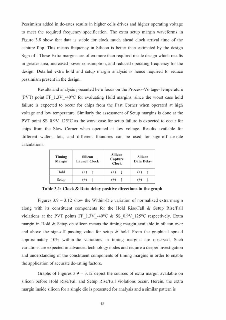
48
Pessimism added in de-rates results in higher cells drives and higher operating voltage
to meet the required frequency specification. The extra setup margin waveforms in
Figure 3.8 show that data is stable for clock much ahead clock arrival time of the
capture flop. This means frequency in Silicon is better than estimated by the design
Sign-off. These Extra margins are often more than required inside design which results
in greater area, increased power consumption, and reduced operating frequency for the
design. Detailed extra hold and setup margin analysis is hence required to reduce
pessimism present in the design.
Results and analysis presented here focus on the Process-Voltage-Temperature
(PVT) point FF_1.3V_-40°C for evaluating Hold margins, since the worst case hold
failure is expected to occur for chips from the Fast Corner when operated at high
voltage and low temperature. Similarly the assessment of Setup margins is done at the
PVT point SS_0.9V_125°C as the worst case for setup failure is expected to occur for
chips from the Slow Corner when operated at low voltage. Results available for
different wafers, lots, and different foundries can be used for sign-off de-rate
calculations.
Timing
Margin
Silicon
Launch Clock
Silicon
Capture
Clock
Silicon
Data Delay
Hold (+) ↑ (+) ↓ (+) ↑
Setup (+) ↓ (+) ↑ (+) ↓
Table 3.1: Clock & Data delay positive directions in the graph
Figures 3.9 – 3.12 show the Within-Die variation of normalized extra margin
along with its constituent components for the Hold Rise/Fall & Setup Rise/Fall
violations at the PVT points FF_1.3V_-40°C & SS_0.9V_125°C respectively. Extra
margin in Hold & Setup on silicon means the timing margin available in silicon over
and above the sign-off passing value for setup & hold. From the graphical spread
approximately 10% within-die variations in timing margins are observed. Such
variations are expected in advanced technology nodes and require a deeper investigation
and understanding of the constituent components of timing margins in order to enable
the application of accurate de-rating factors.
Graphs of Figures 3.9 – 3.12 depict the sources of extra margin available on
silicon before Hold Rise/Fall and Setup Rise/Fall violations occur. Herein, the extra
margin inside silicon for a single die is presented for analysis and a similar pattern is

49
Figure 3.9: Normalized Hold Rise Extra Margin on Silicon depicting Within Die
Variations & constituent components
Figure 3.10: Normalized Hold Fall Extra Margin on Silicon depicting Within Die
Variations & constituent components

50
Figure 3.11: Normalized Setup Rise Extra Margin on Silicon depicting Within Die
Variations & constituent components
Figure 3.12: Normalized Setup Fall Extra Margin on Silicon depicting Within Die
Variations & constituent components

51
observed for different dies within the wafer. An analysis of test results reveals that Hold
which is passing with 0ps of positive slack in sign-off is showing margins in Spice and
Silicon. The reason for this extra margin is pessimism in clock and data de-rates.
Directions of positive value in graph can be interpreted from Table 3.1 which shows the
comparison of silicon data with respect to sign-off. ' ↑ ' represents an increase in silicon
delay with respect to sign- off, whereas ' ↓ ' represents a decrease in silicon delay with
respect to sign-off. When Silicon Clock and Data delays are in the directions of the
arrows shown in Table 3.1, then extra margin for clock and data is in positive direction.
As shown in Figures 3.9 & 3.10, data de-rates are more pessimistic as
compared to clock de-rates for hold. For sign-off Hold, Launch clock is de-rated with
negative value which will decrease the Launch clock delay and capture clock is de-rated
with positive value which will increase the capture clock delay. Therefore we infer that
Clock cells are delayed in silicon with respect to sign-off clock insertion values. Overall
clock de-rates are also pessimistic as skew introduced because of de-rates supports hold.
Spice data which is without any margin is showing positive slack & Silicon result is
above Spice as FF Silicon wafer is towards typical side of the Gaussian curve.
Similarly as seen in Figures 3.11 & 3.12, setup which is passing with 0ps of
slack for a given frequency is having positive slack in Spice and Silicon. Data de-rates
are optimistic with respect to silicon data path/cells and clock de-rates are pessimistic
with respect to clock paths/cells. Sign-off Capture Clock cells are de-rated negatively
for setup which means clock insertion will be faster for capture clock but in silicon
clock cells are having higher delay. This creates more gaps between actual silicon value
and sign-off estimates. Launch path cells are delayed in sign-off with higher de-rates
than silicon which again creates positive skew, supporting the setup. Keeping in mind
that modern technology nodes are slated to be in production at multiple foundries, the
de-rating factors applied must also take into account the lot-to-lot and Fab-to-Fab
variations.

52
3.6 Summary
This chapter presents a test circuit for accurate characterization of delays in
clock and data paths for evaluating the extra timing margin available in silicon.
Understanding the sources of extra margin aids in precisely establishing de-rate added
during sign-off such that fail-free operation can be ensured while deriving maximum
performance from a given circuit. The proposed design uses only standard cells, which
allows for easy implementation. The presented test structure can be used as sensor
inside the chip along with SOC designs to improve the frequency of a design in post-
silicon tuning after reading results from the sensor. The design and methodology
presented in this paper has been tested and validated for the 28nm FDSOI node,
enabling accurate de-rating while taking into account PV effects. In the future, this
block is intended to be deployed for the assessment of even smaller technology nodes to
enable the acceleration of the process development phase.

53
4 ADAPTIVE WEAROUT
MANAGEMENT WITH
IN-SITU AGING
MONITORS
“Live as if you were to die tomorrow;
learn as if you were to live forever.”
Mahatma Gandhi
Abstract: This chapter shows the fundamental elements towards an Adaptive Wearout Management (AWM) control loop for the dynamic supply voltage regulation of digital circuits. Firstly, a new generation of in-situ monitors which generate warning flags to prevent circuit failure under nominal conditions have been explained. A voltage management control loop to efficiently tackle all voltage margins over a large range of DVFS operating conditions and temperatures has been implemented. The relevant experimental silicon results related to timing windows and power savings have been provided.

54
4.1 Introduction
The doubling of transistor counts every two years, as evinced by Moore’s law
[1], has been the fundamental driver of the microprocessor industry. This law still paces
the device roadmap, as defined within the ITRS consortium [75]. Its corollary about
microprocessor performance and power consumption is known as Dennard’s scaling
[76]. In the mid-2000s, this trend was disrupted when the microprocessor reached the
heat dissipation limits of the chip. At this point new solutions (like multiprocessing)
were adopted to keep exploiting the still growing number of transistors, while
maintaining power consumption within manageable limits. On the other hand, the
demand for increasing performances of portable devices like smartphones or tablets is
constrained by a limited power source. Finally, almost all electronic market segments
are now driven by energy efficiency (performance per watt) and not solely by pure
performance metrics. All conventional synchronous digital systems are semi-custom
designs. It means that a set of logic gates is dynamically selected from a standard cell
library (containing all available logic gates) to establish the desired functionality under a
given frequency, while optimizing iteratively power and area consumption. Further, it is
also important that correct timing is ensured under Process, Voltage and Temperature
fluctuations as well as Aging (PVTA). The traditional approach is to fulfil all these
requirements under the worst-case scenario. This worst-case approach translates into
additional voltage safety margins on top of the nominal minimum voltage i.e. the
required supply voltage if no PVTA variations occur as shown in Figure 4.1.
Figure 4.1: Different voltage margins in addition to the nominal minimum voltage

55
Though these margins allow the proper operation in extremely uncommon
scenarios, it results in excessive margins during standard operating conditions, which in
turn deteriorate the circuit’s energy efficiency. Considering the need for growing
margins in recent technologies, it is desirable to cut unused voltage margins while
operating away from worst-case situations. Significant power savings can be achieved
by cutting additional voltage margins as the dynamic power decreases quadratically
with the supply voltage and the leakage power reduces even exponentially. However,
reducing the supply voltage increases the path delays and may result in timing errors.
This necessitates the need for having embedded sensors which can detect / predict the
occurrence of timing errors.
The idea behind circuit failure prediction is to forecast the occurrence of a
failure during normal system operation before the appearance of any error that can
result in corrupt system data and states. This is in contrast to classical error detection
where a failure is detected after errors appear in system data and states. Failure
prediction can be performed in multiple ways wherein the basic principle is to insert a
wide variety of sensors i.e. In-Situ Monitors (ISM) at various locations inside a chip.
During normal system operation, these sensors collect information about various system
parameters over time. Examples of such system parameters range from temperature,
voltage, ring oscillator delays to complex relative timing relationships among logic
signals. The data collected by the sensors is analysed on-chip or off-chip to identify
anomalies and predict failures. In-situ monitors (ISM) might be needed for two main
application kinds. One application is to predict all timing failure events which can be
combined with any existing resilience mechanism [8, 77, 78] at the price to additional,
complex circuitry. Another possible application is to use the monitor as speed sensors
indicating whether stabilized current operation condition is close to possible timing
failure. Except for fast transient voltage variations, this approach can be used with
Adaptive Body Bias (ABB) or Dynamic Voltage Frequency Scaling (DVFS) to account
for static or slowly changing variations such as manufacturing variations, ambient
conditions as well as circuit aging effects.

56
4.2 State of the Art
Margins related to manufacturing variations (towards slow or fast global
corners) can be reduced statically by testing a part after production to adjust the voltage.
This process still does not eliminate the need for margins to cope with dynamic
environmental variations. To exploit unused margins, but avoid aggressive voltage
scaling, the supply voltage has to be adjusted in a closed-loop control. To reach the real-
time feedback of the chip’s operating condition, various classes of monitors have been
proposed in order to measure the circuit path delay. Ring oscillators [79] or Canary
circuits [80, 81] aim to replicate the timing behaviour of the original circuit. Replica
elements are non-intrusive and are well suited for monitoring global variations on the
chip. However, they might fail to capture within-die variations which are local to real
circuits such as random manufacturing variations and circuit aging. Another approach to
overwhelm this drawback is the use of in-situ monitors which aim to measure the timing
slack, directly linked to circuit path delay. Since critical paths typically ends at registers,
the common approach is to use modified flip-flops as slack monitors.
Figure 4.2: Different In-situ delay monitor schematics

57
In Razor approach [8, 82, 83], special latches or flip-flops are used to detect
timing failures due to setup time violation and the voltage adaptation is based on the
monitored error frequency. Errors are corrected through a pipeline flush or architectural
replay by the means of dedicated circuitry. The Razor concept however suffers from
inherent problems, like the large complexity for the necessary recovery mechanisms.
Further problems are the lack of real-time capability and the minimum delay constraint,
which is similar to the hold-time constraint in latch-based designs [82, 84]. The issues
related to error detection scheme can be avoided by preferring circuit failure prediction
approach, i.e. to predict the occurrence of a failure during normal system operation
before the appearance of any error in system data and states. In this approach, enhanced
monitors are used to emit flags (pre-error warnings) when late but still non-erroneous
data transitions occur [85]. The pre-error rate is an indicator for the circuit speed and is
used for local variations and aging aware voltage adaptation. In previous works,
monitors were inserted either at the end of critical paths [85, 86] or at intermediate
nodes [87].
The work described in this chapter uses a new in-situ pre-error monitor [88]
which allows achieving high monitoring performance with minimum overhead, timing
impact and failure rate with respect to previous solutions [85-87]. Figure 4.2 shows the
schematics of different in-situ monitoring solutions. At the top of the figure, a standard
pre-error monitor solution inserted at the end of the critical path is shown. In the middle
of Figure 4.2, the monitor is inserted at an intermediate net with gates having matching
delay. Lastly the bottom of the figure shows the monitoring mechanism used in this
work for implementing an adaptive wearout management scheme.

58
4.3 Monitoring System – Design Perspectives
Figure 4.3: Pre-error monitor schematic
The monitor principle is to minimize both the timing impact on the monitored
critical path and the source of within-die variations. The generic monitor schematic
shown in Figure 4.3 can be straightforwardly compared to previously proposed
monitors [85-87]. The main idea is here to probe the incoming data right after the
master latch [88] (and not prior as all previous approaches) in order to get rid of the
additional load related to the monitor on the already critical path. Through adequate
sizing of the delay element, it is possible to minimize the impact on the flip-flop setup
time. Figure 4.3 shows a detailed schematic of the real monitor implemented and
utilized for the work described in this chapter. The delay element is composed of
minimum size inverter and a multiplexer so to allow a Test Mode (TM). The delayed
signal is then passed through an additional latch, equivalent to the Slave latch of the
reference flip-flop. At this stage, it can be concluded that this approach is more efficient
in terms of area overhead than other approaches [85-87] that are using at minima a
duplicate of the whole reference flip-flop. In the implementation used in this work, a
second latch have been introduced to act as an additional delay element, thus enabling
two different monitor detection window at the price to larger monitor area overhead.

59
Figure 4.4: Timing diagram for Pre-error monitor
The timing diagram for the monitor is shown in Figure 4.4. From left to right,
the Data (D) is more and more delayed with respect to the clock (CLK) though the flip-
flop output Q remains correct. In the first configuration, no warning flags are emitted
since the remaining slack is large enough. For slightly reduced slack (intermediate
situation), only the Flag2 is raised (corresponding to the large timing window) while
Flag1 remains at zero. Finally, when the slack is further reduced, both Flag2 and Flag1
are raised.
To evaluate experimentally the proposed monitoring system, a Bose, Ray-
Choudhary and Hocquenghem (BCH) [89] error correcting code IP core consisting of
encoder and decoder modules has been implemented with in-situ monitors (ISM)
appended at the end of critical paths. The decoder module makes use of the following
algorithm:
1. Calculate the syndromes for the received frames
2. Determine the number of errors and their location using the Chien search
algorithm
3. Calculate the error values at those error locations and
4. Correct the errors.
Random frames and errors are generated using Pseudo Random Binary Sequence
(PRBS) modules to emulate a large range of patterns. The overall BCH IP is
implemented with an autotest module which raises an Autotest_OK flag when the
decoding process (including error localization and correction) proceeded without

60
failure. The BCH IP core was implemented in 28nm UTBB FDSOI technology using
standard design platform flow and tools. The IP consists of 8469 gates for 869
endpoints and 1720 critical paths.
Figure 4.5: Path delay histogram for BCH IP at different conditions of voltage &
process
While using in-situ monitors, the primary questions relate to where and how
should the monitors be inserted. The monitor insertion requires first a placed and routed
reference design (i.e. without monitors). From that reference design, the path delay

61
histogram can be extracted under various Process, Voltage, Temperature and Aging
(PVTA) conditions as shown in Figure 4.5. Any circuit is designed with the intent to
work at a given operating clock period which is guaranteed in a generic flow under
worst-case conditions (i.e. including all margins). As a matter of fact for typical corner,
there is some room for either performance increase (i.e. frequency) or power reduction
(i.e. voltage reduction). In both cases, all paths whose worst-case delay falls in the flag
detection window (paths highlighted in red in Figure 4.5) are classified as timing critical
and require monitors. In the Figure 4.5, the top graph shows the path delay histogram of
the BCH IP at typical corner and nominal voltage; the middle graph is plotted for
minimum voltage (Vmin) and typical corner; whereas the bottom graph is for minimum
voltage (Vmin) and worst-case corner.The size of the flag detection window affects the
total number of monitors and the monitoring area overhead is directly proportional to
the flag detection window. In this work, four versions of the BCH IP have been
implemented depending upon the number of monitors. The implementation results are
summarized in Table 4.1.
Table 4.1: Implementation results of BCH IP with in-situ monitors

62
4.4 Results and Analysis
This section firstly depicts the results of the silicon validation of the embedded
in-situ monitors. Thereafter an Adaptive Wearout Management strategy implemented
using the warning flags from the in-situ monitors is explained with the associated
results. Finally the power savings achieved via implementing the AWM control loop are
enumerated.
4.4.1 In-Situ Monitors
Figure 4.6: Experimental timing diagram showing pre-error flags behavior with
lowering voltage
All experimental results presented in this section are from the BCH1
implementation, except when stated differently. The overall BCH IP core is
implemented with an autotest module which raises an Autotest_OK flag when the
decoding process (including error localization and correction) proceeded without
failure. Overall, experimentally, the occurrence of the Autotest_OK flag and warning
flags (Flag1 and Flag2) under various PVTA conditions and PLL frequencies are the
main parameters monitored with the Leakage and Dynamic powers. Figure 4.6 shows
the experimental timing diagrams observed on the Verigy 93K tester. For a given
voltage value, only the Flag2 (with the biggest detection window) is raised while
Autotest remains OK and the Flag 1 is not raised (top). If the voltage is lowered, both
Flag1 and Flag2 are raised, which illustrates that the critical paths are close to failure

63
(bottom). Yet, the Autotest_OK flag, here raised, states that the pattern executes without
failure.
Figure 4.7: Experimental warning flag/BCH1 Autotest maximum frequencies for
various PVTA conditions
By varying PVTA conditions, the maximum frequency is searched for both the
Autotest_OK flag and the Flag1, Flag2 warning flags. For BCH Autotest, the maximum
frequency corresponds to the highest frequency for which the PRBS pattern runs
without failure under the given PVTA conditions. For warning flags, the maximum
frequency corresponds to the highest frequency for which the pattern runs without
triggering a warning flag. Both maximum frequency measurements can be compared in
a correlation plot as shown in Figure 4.7. The important element here is that warning
flags are mostly always emitted prior to the actual BCH IP core failure, thus acting as
pre-error flags. The usage of in-situ aging monitors is also motivated by the possibility
to correct inline for aging-related drifts. As a matter of fact, adding such monitors into
an IP should not introduce additional failure rate. With pre-error monitors approach, the
risk is related to the presence of false flags, i.e. a warning flag occurring after the actual
failure of the IP. By construction, the pre-error monitor provides some margin (the
delay element) as illustrated in Figure 4.7 where in average warning flags are always
emitted prior to the actual BCH IP failure. The warning flags detection window can be
experimentally measured directly by comparing the warning flags and BCH Autotest
maximum frequencies.

64
4.4.2 Adaptive Wearout Management
Figure 4.8: Adaptive Voltage Management Flowchart
In the proposed Adaptive Wearout Management (AWM) scheme, the supply
voltage is controlled according to the occurrence of in-situ monitor flags. The basic idea
is to reduce the voltage as long as no warning flags are detected for a given observation
interval Ncycles. Otherwise, in presence of detected flags, the voltage is increased. The
flowchart of the implemented voltage management scheme with 1mV regulation step is
shown in Figure 4.8. From recent studies, increasing the voltage to provide additional
margin has proven to be efficient [90-92] to manage additional margins with respect to
reliability. By reducing the supply voltage, the delay distribution is shifted towards

65
longer timings, as shown in Figure 4.5. At some point, some timing paths will be lying
in the in-situ monitor detection window and as a consequence, they can trigger a
warning flag. For a fixed operating condition and for a long execution time, the patterns
running through an IP can be seen as randomly distributed. To emulate this situation
experimentally, patterns at the inputs of the BCH IP core are generated using Pseudo
Random Binary Sequence (PRBS) modules, as described earlier.
Figure 4.9: Adaptive Wearout Management (A) without considering aging effects
and (B) With considering aging effects
Using this simplified scheme, several AWM control loop configurations have
been explored i.e. with different nominal voltage & frequency as well as different
regulation step sizes. At first, a typical, fresh (i.e. no aging) part is observed and the

66
initial voltage is the one resulting from the overall voltage margin stacks as described in
Figure 4.9(A). After some use time, as a result of the AWM control loop, the voltage
reaches a steady state voltage value which is close to the minimum voltage, while still
executing the instructions without failure. This steady-state value is defined by the in-
situ monitor (ISM) delay margin, as introduced by design. The steady-state voltage
values are distributed around an average value which is observed to be independent of
the voltage regulation step. Following an electrical stress, all the degradation modes will
induce a speed slowdown. This is illustrated in Figure 4.9(B) where the minimum
voltage to sustain a given frequency after aging is increased compared to the fresh
situation. This illustrates that the AWM control loop is still efficient after aging to adapt
the voltage.
Figure 4.10: Detection window evolution with stress time
As stated in [93], the impact of electrical aging degradation in digital circuits
should not only consider the average degradation but also the induced additional
variability. To evaluate this impact, the Flag1 detection window degradation has been
monitored along the stress, considering both the average value and its standard
deviation as shown in Figure 4.10. It is worth noticing that its standard deviation is also
increasing with stress time as a result of the degradation-induced variability in the
monitor.

67
4.4.3 Power Savings
Figure 4.11: Monitoring system failure rate and power reduction for various
DVFS operating conditions
Figure 4.12: Total power savings with respect to static voltage margin at different
temperatures
As a result from the AWM control loop, the fresh (i.e. no aging) parts can
operate at much lower voltage, so with power savings with respect to a conventional
static voltage margin. The experimental power savings under worst-case conditions (i.e.
higher temperature) have been measured to be 36% for static power (i.e. leakage) and
25% for dynamic power over 0.5-2.0 GHz frequency range for Flag1 detection window
as shown in Figure 4.11. Over this large range of frequency, the worst-case supply

68
voltage is dynamically following the frequency change in a dynamic way through a
DVFS approach. In all these operating conditions, it is worth noticing that the
monitoring system has negligible failure rate. The total power savings is reduced with
lower temperatures for a given monitor layout as shown in Figure 4.12. This is due to
the fact that, at lower temperatures, the relative impact of the leakage power is reduced
from 20% at 125°C to 5% at -40°C.
4.5 Summary
This chapter demonstrated the fundamental elements towards an Adaptive
Wearout Management (AWM) control loop for the dynamic supply voltage regulation
of digital circuits. Firstly a new generation of in-situ monitors which generate warning
flags to prevent circuit failure under nominal conditions have been explained. The
adaptive voltage management control loop is efficient to tackle all voltage margins on
fresh parts (i.e. without aging) over a large range of DVFS operating conditions and
temperatures. In spite of the performance degradation after an electrical stress, the
AWM control loop is still efficient to maintain a fault-free instructions execution with
consequent power savings over the whole lifetime. Overall, up to 40% static and 25%
dynamic power reduction has been demonstrated over a large range of DVFS operating
conditions while maintaining a fault free instruction execution.

69
5 THERMAL
CHARACTERIZATION USING
DIGITAL SENSORS
“If you want to shine like the Sun,
first burn like the Sun.”
A. P. J. Abdul Kalam
Abstract: Post-silicon thermal validation of fabricated chips is necessary to ensure safety, reliability and conformity to specifications. Because of the enormous complexity of modern designs, it becomes mandatory to accurately characterize thermal behaviour during the technology development phase itself. In this context, this chapter presents a test methodology for thermal characterization under dynamic workloads using embedded digital sensors. Firstly the design of the test-chip used is explained and thereafter the test patterns and test methodology employed are elaborated upon. In particular, the methodology required for managing high volume of data generated during such tests is elaborated upon. Analyses of the on-chip thermal results provide useful insights for test-chip design requirements related to thermal measurements.

70
5.1 Introduction
In recent years elevated on-chip temperatures have become a major concern in
the design and operation of computing devices. Magnitudes of on-die temperatures are
determined by the spatial and temporal allocation of power consumption and the design
of the heat removal system. Elevated temperatures directly impact all key circuit metrics
including: lifetime and reliability, speed, power, and costs. Hot spots reduce the Mean
Time to Failure (MTF) as most failure mechanisms (e.g., electromigration, time
dependent dielectric breakdown, and negative bias temperature instability) have strong
temperature dependencies [94]. Furthermore, different thermal expansion coefficients of
chip materials cause mechanical stresses that can eventually crack the chip/package
interface [95]. Elevated temperatures also slow down devices and interconnects leading
to timing failures [96, 97]. The exponential dependency of leakage power on
temperature further increases total power and could lead to thermal runaway [98]. Due
to the non-ideal scaling of power consumption and costs of heat removal systems,
temperature has become a major hurdle towards improving the performance of high-end
many-core processors [99]. Moreover due to the enormous complexities and sheer
number of modelling parameters of state-of-the-art designs, pre-silicon power and
thermal models cannot be trusted blindly. It is necessary to complement pre-silicon
analysis with post-silicon thermal and power characterization on the fabricated devices,
and then to use the characterization results to improve the design during re-spins before
ramp-up and production. In this context, the work of this chapter describes a test
methodology for accurate thermal characterization under dynamic workloads using
embedded on-chip thermal sensors.
5.2 Test-chip Design Overview
The test-chip used for thermal characterization under dynamic workloads is
fabricated using the 28FDSOI process technology. From the viewpoint of performing
Self-Heating measurements, the test-chip embeds within itself a PLL for high frequency

71
generation, various versions of the BCH IP (explained in Chapter 4) which is a
representative digital block used to emulate dynamic workloads, and a Thermal Sensor.
Figure 5.1: Floor plan and overview of test-chip used for thermal characterization
Figure 5.1 shows the floor plan & overview of test-chip used for thermal
characterization. The main elements of the test-chip used for performing self-heating
measurements are briefly described hereunder:
· BCH IP: Six instances of the BCH (Bose, Ray-Choudhary and Hocquenghem)
error correcting IP have been included in the test-chip. From the point of view of
performing self-heating measurements, the BCH is a representative digital block
consisting of 8469 gates wherein activity can be triggered at high frequency.
Additionally an Autotest mode exists which triggers activity by generating
frames using a pseudo-random generator.
· PLL: An on-chip charge pump Phase Locked Loop (PLL) is used to clock the
BCH IP at high frequencies. The PLL is suitable to produce output frequencies
in the Ghz range above the maximum operational frequency limit of the BCH
IP.
· THS: The thermal sensor embedded within the test-chip has a design range for
temperature measurement from -40°C to 125°C with a resolution of 1°C. The

72
measured temperature is computed by reading a digital code on the top level
pins of the test-chip.
Various blocks are muxed together within the test-chip to overcome the constraint
of having limited number of IO pads for multiple blocks. Hence, the same top level
input pins are used for activating different functions on different blocks. Similarly
the outputs of these different blocks are mapped to overlapping output test pins.
Also the power supplies for the BCH, PLL & THS are muxed together on a single
tester channel due to hardware limitations. These design constraints introduce
additional complexity in the pattern generation and output data observation.
5.3 Test Patterns
Two distinct patterns and their associated test methods have been developed to
understand the effect of static & dynamic heat. Static heat is referred to as the thermal
temperature measured using the sensor when there is no activity triggered on the other
blocks within the test-chip. While dynamic heat is used to refer to the measured
temperature when activity is induced on the neighboring blocks of the test-chip.
· Pattern for Static Self Heating Measurements
Figure 5.2: Pattern for Static Self Heating Measurements
Figure 5.2 depicts the outline of the pattern used to perform static self-heating
measurements. Measurements are made and the sensor reading is recorded at multiple
voltages with all other blocks within the test-chip having no activity induced on them.
These measurements help gauge the impact of switching activity on heat measurements.
· Pattern for Dynamic Self Heating Measurements
Figure 5.3: Pattern for Dynamic Self Heating Measurements

73
Figure 5.3 depicts the outline of the pattern used to perform static self-heating
measurements. The different parts of the pattern are explained hereunder:
1. Initially the THS is activated and a single measurement is performed to acquire
the value of static temperature without the PLL or BCH being activated.
2. In the second step the PLL inputs are set to produce the desired frequency. At
this stage of the pattern, the input configuration of the PLL is latched and
thereafter any change on the input pins of the PLL block has no effect on the
PLL output frequency as long as the input clock is stable & well functional.
Once the PLL Output frequency has stabilized, a status signal goes high. A
digital Capture is performed to ascertain the state of the PLL status signal in
order to ensure that the BCH blocks thereafter are clocked at the correct
frequency.
3. In the third stage, the THS is once again activated and a single measurement is
acquired to see if there is any effect on temperature due to PLL activation.
4. In the fourth stage, the required BCH blocks are activated and a single digital
capture is performed to check the Autotest status and verify BCH functionality
at the set voltage & frequency.
5. In the fifth stage, the THS is activated with the BCH still running at the set PLL
frequency with the outputs configured to observe the Thermal sensor data. This
stage of the pattern is kept in a loop so that the duration for performing dynamic
self-heating measurements can be easily configured by setting the loop counter
for this stage.
6. In the sixth stage, a simple BCH Autotest check is performed with the value
being acquired via a single digital capture to check the BCH functionality after
Self-Heating measurements have been completed.
7. In the final stage, the PLL functionality is once again verified via a single digital
capture on the PLL status signal to ensure that the PLL was well functional
while the dynamic self-heating measurements were in progress.
An important aspect for patterns which activate multiple blocks as in this case is that the
PLL & THS need to be simultaneously provided with different clock frequencies using
a single spec. This is managed at a binary level within the pattern editor and the
resulting clock waveforms are shown in Figure 5.4.

74
Figure 5.4: PLL and THS Clock Waveforms
5.4 Selective Digital Capture Methodology
Figure 5.5: Memory management during Digital Capture [100]
For effective thermal characterization, the test methodology must be capable of
acquiring large amounts of digital output data of a device at a high data rate and storing
this data for later analysis and processing. This section briefly explains the usage of the
SmarTest [100] digital capture test methodology for our particular test case. For digital
capture, as the size of the Sequencer Memory (SM) is limited as compared to the Vector
Memory (VM), it is essential that the pattern be placed in the SM as the captured data
can then stored in the VM as shown in Figure 5.5. During execution, the sequencer
reads the pattern from the SM and stores the captured data in the VM.
In order to read the values of the THS, it is necessary to perform periodic
digital captures. HP SmarTest provides two distinct modes for digital capture namely
the Sequential mode and the Selective mode. The default mode for Digital Capture is

75
the Sequential mode wherein the Tester captures all output samples on all output pins
for every Tester cycle of the pattern length. The Sequential mode is not suitable for
capturing data in this case as capturing starts with the first vector and ends with the last
vector of the main pattern. This causes a memory overflow by capturing output data
which is not used for further processing. In such a scenario, SmarTest returns an
available capture memory overflow message as shown in Figure 5.6.
Figure 5.6: SmarTest Memory Overflow Message
In order to overcome this memory limitation, it is essential to employ the
Selective Capture mode wherein capturing will be only carried out at vectors with
device cycles containing designated capture edge actions. Using selective mode,
capturing of undesired data can be completely suppressed i.e. only specific vectors
within a pattern may be selected for capture. Selective capture mode is automatically
activated when the pattern used for digital capture incorporates two specific edge
actions in the wavetable to define when and when not capturing will be performed:
· Action C à Capture data on this edge.
· Action D à Do not capture data on this edge.
The aspects that need to be kept in mind when defining a selective capture are listed
below:
1. The number of selective capture edges must be the same for all selective capture
waveforms in one wave table. Within a capture pattern (label) selective capture
actions need to be on the same receive edges across all waveforms of the
according wave table.
2. Each waveform within a capture pattern (label) must contain either "C" or "D"
actions consistently over all used capture receive edges. A waveform that
contains a "C" or "D" action must not contain any other compare action.
3. The edge that is used for selective capturing must be set explicitly to "D" in all
waveforms of the wavetable where it is not to be captured. This also applies to
the waveforms for the default device cycle.
4. The "C" action will perform a 'compare to 0' to determine the capture value.

76
5. In the same wavetable C and D actions cannot be mixed with other receive
actions.
6. C or D actions cannot be mixed with other receive actions within one waveform.
7. The selective capture actions C and D cannot be mixed within one selective
capture waveform.
8. If the number of selective capture edges is n, the edges r1 to rn must be defined
in each selective capture waveform in one wavetable.
9. The selective capture actions C & D must be placed only on the receive edges of
Output Pins. On the same receive edges in the input pins, the action “N” may be
specified.
Figure 5.7 shows the Selective Capture wavetable employed for the pattern using
which dynamic self-heating measurements are done.
Figure 5.7: Selective Digital Capture Wavetable
Further, the patterns that contain digital capture actions ('capture' and 'do not
capture') must be associated with test methods, which do not execute functional tests.

77
The Sequential/Selective Capture mode cannot be selected in the capture
settings GUI of the Pattern Editor. The active mode is determined by the selected
capture pattern. If the vector label uses a wavetable that contains selective capture
actions (C & D), the Selective mode is activated.
In order to retrieve the captured data after a Digital Capture Test has been
performed, vector variables must be used which allow us to define an arbitrary subset of
the captured data. By defining several vector variables, it is possible to retrieve different
views of the same captured data. It is important to note here that the vector variables
along with their configuration parameters (no_of_frames, vector_interdiscard etc.) only
define how to extract (filter) the data of interest from the captured data. Further, vector
variables are always related to one specific pattern and cannot be used with another one.
Figure 5.8 shows how a vector variable and associated configuration parameters may be
used to retrieve a subset of the captured data.
Figure 5.8: Example of a Digital Capture Variable with associated parameters
[100]

78
5.5 Results and Analysis
This section firstly depicts the thermal measurement results and thereafter
provides future directions related to test-chip design for efficiently characterizing self-
heating under dynamic workloads.
5.5.1 Results Summary
Figure 5.9: Thermal Characterization results for Static & Dynamic conditions
Figure 5.9 shows the thermal characterization results for static & dynamic
conditions in the voltage range of 0.9V – 2.0V wherein dynamic measurements are
made at each voltage point for 50 seconds. In Figure 5.9, the first 50 seconds
correspond to 0.9V, the time from 51-100 seconds corresponds to a voltage setting of
1V and so on. The Thermal Sensor displays good functionality across the entire
operating temperature range, however no apparent effect of dynamic activity is
observed in the THS output. From the results it can be reliably concluded that the
observed rise in temperature is completely due to higher voltage applied on the Thermal
Sensor itself as all supplies for the PLL, BCH & THS are clubbed together on a single
channel within the probe-card and it is not due to any dynamic activity on the BCH
blocks.
5.5.2 Analysis and Future Directions
This sub-section elaborates on the possible reasons for relative constant
temperature across static and dynamic modes and the directions for future investigation.

79
1. The tests are performed at Wafer Level where there is a high possibility of heat
dissipation. Possible reasons could include thick substrate and no spatial
isolation. Future work should involve performing tests on packaged dies.
Note: No packaged dies of the test-chip under consideration were available for
this work.
2. Resolution of the THS is 1 degree which is not sufficient to observe Self–
Heating at the wafer level with the required granularity. Embedded sensors with
higher resolution should be considered for similar characterization works.
3. The BCH blocks on which activity is induced occupy a very small area within
the test-chip to induce any appreciable self-heating effects. Also the thermal
sensor is located at the corner of the test-chip as shown in the floor plan of
Figure 5.1. In the future, the thermal sensor should be ideally located within the
chip such that it is spatially surrounded by larger activity inducing blocks.
5.6 Summary
This chapter presented a test methodology for thermal characterization using
an embedded digital sensor. Firstly the test pattern structure for self-heating
measurements of the test-chip under consideration is given. Thereafter the methodology
focusses on efficient memory management during silicon testing. Although the
measured results were unable to capture the impact of dynamic activity on self-heating,
the developed methodology is generic in nature and can be utilized for different
applications which deal with memory intensive measurements. Finally the directions for
future work are elaborated upon for accurately capturing the impact of switching
activity on chip temperature.

80

81
6 SIMULATION AND SILICON
VERIFICATION OF ADAPTIVE
VOLTAGE SCALING
“If you torture data long enough,
it will confess to anything you like.”
R. H. Coase
Abstract: Process variation causes measurable and predictable variance in the output performance of all chips. Adaptive Voltage Scaling (AVS) is now a key power management feature which is applied by reducing the voltage of fast silicon, to a point where speed target (Fmax) is met, thereby reducing power consumption. This chapter presents the full silicon level electrical characterization correlation of the simulation done using a novel method based upon existing CAD tools & a mixed mode approach, enabling complete Process-Voltage-Temperature (PVT) characterization on the portion of the design for which AVS is defined. The observed results on silicon for the metrics of performance & power display a close correlation with the ones obtained via the simulation flow, thus providing designers with deeper insights into the gains with AVS from within the simulation.

82
6.1 Introduction
Modern CMOS processes vary in performance from die to die and wafer to
wafer. Process variation causes measurable and predictable variance in the output
performance of all devices but becomes particularly important at smaller process nodes
[28, 29, 58-61]. This phenomenon occurs on all semiconductor devices from all
manufacturers and is more relevant for smaller semiconductor technology nodes or
geometries. Different process corners represent the variation in attributes of integrated
transistors when a semiconductor device is fabricated. Process corners can be loosely
classified into the three following categories:
· Slow (SS): A device fabricated with the slow process corner provides the lowest
acceptable frequency performance allowed at nominal voltages. Slow devices do
not have the potential to run at higher frequencies beyond the specified nominal
frequency. Slow devices typically consume less leakage power than others
devices in the population distribution.
· Typical (TT): A typical device operates at the midpoint or average frequency
performance across the population of devices at nominal voltages. Typical
devices have average performance when compared to slow and fast devices.
· Fast (FF): A fast device provides the highest performance across the population
of devices. Fast devices have the potential to run at faster frequencies than are
required at nominal voltages. Fast devices can operate at the minimum specified
frequency at voltages lower than nominal voltage values. However, fast devices
exhibit more leakage power consumption than slow and typical devices,
especially during high temperature conditions.
However the exact extent of variation is not always known prior to fabrication since
designers are provided with a worse case set of parameters to use for timing closure
simulation with the operating voltage which takes into account the slowest silicon.
With the emphasis on achieving lower power consumption a concern for
system designers, Adaptive Voltage Scaling (AVS) [72, 73] is now a key power
management feature that enables power reduction through voltage reduction. AVS is the
adaptation or modification of the supply voltage for a chip depending upon its process
corner. In the most basic form, Dynamic Power consumption for digital circuits can be
considered as P = CV²F where C is the switching capacitance, V is the supply voltage,

83
and F is the clock frequency. The leakage power is also voltage dependent. Therefore
significant power savings can be made through AVS which delivers accurate voltage to
each individual chip across temperature, process corner, and frequency variations.
Figure 6.1: Basic representation of power savings through adaptive voltage scaling
AVS is applied by reducing the voltage of a chip coming from a fast corner to a point
where speed target (Fmax) is met, thereby reducing power consumption as shown in
Figure 6.1. Because of process variations, the supply voltage of each device can be
adjusted to minimize power while still achieving desired performance. In order to
evaluate power gain for a digital circuit using AVS, it is necessary to evaluate Speed
and Power at multiple PVT points which are in fact different from classic design
development points.
By accurately setting the supply voltage for the actual requirements of each
chip, large power savings can be realized for chips coming from a fast corner. Inversely,
some failing chips below the minimum frequency (Fmin) coming from a slow process
corner can be made to pass by increasing the voltage with the associated penalty of
higher power consumption. It is therefore necessary to evaluate through electrical
simulation, design performance under process and voltage scaling conditions. However,
it has not been feasible to perform electrical simulation for full System on Chip (SoC)
with sufficient accuracy in a reasonable time. The work presented in this chapter,
addresses this infeasibility and proposes a new method that overcomes the major
constraints relating to simulation time and accuracy thereby paving the way towards
accurately simulating the electrical performance parameters of complex MPSOC
designs. A novel method based upon existing CAD tools & a mixed mode approach,
enabling complete PVT characterization on the portion of the design for which AVS is

84
defined. Furthermore, the full silicon level electrical characterization correlation of the
simulation is presented.
6.2 Reference Design
The reference design used for the development of this work is the ‘Area &
Power IP’ (APIP) block which is designed and fabricated in the 28nm technology to
address adaptive voltage scaling. The APIP is a representative design containing a
control and calculation unit with the maximum frequency being greater than 1Ghz and a
voltage range of 0.5V - 1.3V being inline with end product requirements. It is a
programmable power consumption block with the basic elements being 16-bit adders,
subtracters & multipliers. Its design consists of approximately 400k transistors.
Performance characterization of the APIP block enables the understanding and provides
a deeper insight into cutoff frequencies and power supply saving dependencies versus
process variations. This circuit is also useful for leakage and dynamic currents
monitoring on a small design block.
The basic top level block diagram of the APIP is shown in Figure 6.2 and the
main elements are explained thereafter:
Figure 6.2: APIP Basic Representation

85
Figure 6.3: Grouppmm block diagram
· Pace Counter: Power consumption is controlled is via a programmable counter
which allows data to be generated every N cycles (controllable)
· Generator : Generates the signals on the basis of toggling mode selected i.e.
ramp-up, ramp-down etc. Alternately a 16 bit specific external vector can also be
loaded.
· Grouppmm : This module takes the value generated by the generator and applies
two transformations based on addition, subtraction and multiplication as shown
in the Figure 6.3.
The APIP can be considered to be well functional when the following two conditions
are satisfied:
1. HBM i.e. heart beat monitor generates a low frequency, indicating functional
status of the IP. Generated frequency = Input Clock Frequency / 32.
2. Flag_reg remains high unless a mult_flag becomes active or Reference !=
Processed.
In order to enable the APIP to be clocked at high frequency, it is interfaced with an on-
chip low area frequency generator (FreqGen) as shown in Figure 6.4.

86
Figure 6.4: FREQGEN & APIP Interfacing
The FreqGen generates a high frequency clock signal with programmable
frequency and a constant (~ 0.5) duty ratio. The block is used to provide a high
frequency square wave pulse to the APIP. The FreqGen contains a 16 step
programmable ring oscillator & each fundamental frequency can be further divided by 8
division factors. When activated, the frequency available on FreqOut is directly applied
to the APIP. FreqOut/16 is available on the Output Pad of the Test-chip.
Since the FreqGen has 16 fundamental frequencies which may be further
divided, it introduces the limitation that only discrete frequencies can be produced in the
targeted test window. Let FFi, FFi+1, FFi+2, ……. FFn be the range of discrete
fundamental frequencies that can be produced using the FreqGen and DF the division
factor,
It can be clearly seen from the above equation that as the division factor (DF)
decreases and as we move towards higher frequencies, the interval between two discrete
frequencies increases. This introduces a maximum error of approximately 5% in the
final silicon characterization which is computed based upon the difference between the
last passing frequency and the first failing frequency. This needs to be kept in mind
while analyzing the results.
The tradeoff in using a ring oscillator based macro versus a PLL for high
frequency functional characterization lies in the relatively lower on-chip area required
for the FreqGen and the limited discrete frequencies that can be produced.

87
6.3 AVS Simulation Methodology
Figure 6.5: Computation effort for full PVT simulation using Fast Spice
The standard method for full PVT electrical simulation is to load a design data
base along with spice netlist for digital library into a fast spice simulator such as
CustomSim. For AVS simulation, accuracy with less than 2% error or 10mV resolution
is required. This implies fixing maximum accuracy mode and a huge number of PVT
points i.e. 156 PVT configurations, leading to 1560 simulations if we take into account
3 process corners, 13 voltages points, 4 unique temperatures and 10 distinct frequencies
as shown in Figure 6.5. This methodology then intrinsically limits the design size and
the testbench size to small and unrepresentative test cases as the design requires
CustomSim precision of 5 and a simulation run time of 20 hours, leading to a complete
simulation time of 130 days, which is unfeasible and unscalable to large circuits.
The approach utilized for simulation exploits the capabilities of VCS AMS
[74] to address the design size and then applies new simulation techniques to
simultaneously measure Fmax and power within the same simulation run. An additional
step optimizing Fmax search has also been developed. While mix mode simulation for
mixed analog and digital design is well established, solutions for full digital circuit are
generally not required. For this work, firstly the entire circuit was simulated using a
pure spice simulator with an external script to retrieve the results. This enabled to
evaluate the accuracy of the mixed mode approach and also the gain in runtime. In the
particular case of AVS, only a portion of the design requires accurate Fmax simulation,
i.e. the modules containing critical paths. We can take advantage of this fact through
mixed mode simulation where the AVS block is simulated using fast spice and the
remainder of the circuit and testbench is simulated using standard functional simulation

88
i.e. digital simulation using VCS. Furthermore, most digital systems require a
setup/initialization phase followed by a run-mode/calculation phase, and now that a
mixed mode simulation is established, all setup and data extraction portion of the
simulation can now be performed using the faster functional simulator. This approach
leads to a gain of ~7.2X in the total simulation time and is summarized in Figure 6.6.
Figure 6.6: Simulation flows based on CustomSim & VCS AMS
A pass/fail method to locate the Fmax for each given operating point is
developed. This entails running multiple simulations using a standard dichotomy
method, to converge to the FMAX for each given operating (PVT) point. To facilitate
this, features of the simulation ($snps_get_volt command in the digital environment
allows us to retrieve analog values) enabling a feedback from the functional output to
adjust variables for the next simulation are used. This method can be further enhanced
by running multiple simulations in parallel to increase the convergence speed which
enables a rapid convergence to the final functional simulation reporting a Vmin for a
target frequency.
Performance in simulation run times has also been improved using VCS-AMS
through the enablement of direct dynamic power and leakage measurements during the
Fmax search simulation runs. This is an improvement over a more classical approach of
running power simulations at a fixed set of predefined PVT points. Power Measurement
uses analog assertion commands which automatically create the control files required by
CustomSim to post-process the output files. Further simulation time reduction was
achieved while including power variation in the whole test flow, avoiding every

89
preliminary setup phase prior to Fmax search as shown in Figure 6.6. This lead to an
additional gain of ~2X in simulation time, thus leading to a global gain of ~15X in
simulation time. Power variation has been done by changing standard power supply
defined in Spice to a Real number defined directly in the testbench, enabling on the fly
modification of supply voltage during simulation runs. Further gains have been
achieved through a judicious use of simulation features enabling the direct reporting of
the final results.
This is achieved through Fast Spice options which directly extract current
measurements and provide them to the testbench environment, which in turn store them
in output files. Here instead of manually extracting the average current we generate
directly a “.meas command” in a text file with time values obtained from the testbench
itself & then launch automatically Custom Waveview to extract the average current. A
summary of the novel simulation flow enabled using Synopsys tools and the resulting
runtime improvements achieved are diagrammatically shown in Figure 6.7.
Figure 6.7: Simulation methodology overview and resulting Run-time
improvement

90
6.4 Silicon Characterization Methodology
Two distinct and conceptually simple methodologies namely the Fmax &
Vmin searches have been employed for characterization of the APIP block.
· Fmax Search: The voltage is set to distinct values in the design range and the
maximum frequency at which the APIP block is functional is logged.
The following steps are performed for an Fmax Search:
1. The frequencies produced by the FreqGen are precharacterized using a high
division factor i.e. the fundamental frequencies generated by the 16 distinct
steps of the ring oscillator are logged. Using high division factors is required
since a maximum frequency of approximately only 35 Mhz can be reliably
observed and recorded on the output pins of the tester. Therefore the
maximum undivided frequency which can be reliably observed can be
calculated as :
Max Undivided Freq / Output pin divider value = 35 Mhz
! Max Undivided Freq = 35 x 16 = 560 Mhz
Hence it is not possible to observe the entire range of fundamental
frequencies of the FreqGen on the output without using division factors. This
necessitates the pre-characterization of the FreqGen using an internal
division factor in order to overcome the inability to observe in real time the
frequency produced by using low division factors.
2. The desired voltage level along with the fundamental frequency and division
factor of the FreqGen are setup for test.
3. A functional test is performed to check the status of the Flag_reg signal
(Figure 6.2) and the frequency of the HBM signal is measured thereafter.
4. The Pass/Fail results at the particular test point under consideration are
logged.
5. Steps 2 – 4 are performed for the entire range of volatge points, fundamental
frequies and division factors.
6. The values of maximum frequency, static current and dynamic current for
each voltage point are determined from the logged results.
The flowchart for the Fmax search is shown in Figure 6.8.

91
Figure 6.8: Flowchart for APIP Fmax characterization

92
· Vmin Search: The frequency is set using distinct FreqGen configurations and the
minimum voltage at which the APIP block is functional is logged.
The following steps are performed for an Vmin Search:
1. The frequencies produced by the FreqGen are precharacterized using a high
division factor to overcome to hardware limitation of the tester.
2. The desired fundamental frequency and division factor of the FreqGen along
with the voltage level are setup for test.
3. A functional test is performed to check the status of the Flag_reg signal and
the frequency of the HBM signal (Figure 6.2) is measured thereafter.
4. The Pass/Fail results at the particular test point under consideration are
logged.
5. Steps 2 – 4 are performed for the entire range of volatge points, fundamental
frequies and division factors.
6. The values of maximum frequency, static current and dynamic current for
each voltage point are determined from the logged results.
The flowchart for the Fmax search is shown in Figure 6.9.
The intent behind developing two distinct test methodologies was to verify the
stability & reproducibility of the results achieved when the APIP is clocked with the
ring oscillator based FreqGen. Additionally the idea was to also analyse the impact
of discrete fundamental frequencies on the precision of the result since a higher
degree of granularity is available when doing a Vmin search at the available discrete
frequencies. It was observed that the characterization results from these two
methodologies displayed exact correlation. However since the test time for
implementing a Vmin search is much larger than an Fmax search with no visible
benefit in accuracy, the Fmax search method was used for the full wafer
characterization at different PVT points.

93
Figure 6.9: Flowchart for APIP Vmin characterization

94
6.5 Results & Analysis
In terms of analyzing the simulation vs silicon correlation, the metrics of
interest are the maximum frequency, leakage current & dynamic current at a particular
voltage. For if there is a good correspondence on these metrics, one can reliably predict
the power consumption & thereby the power savings through AVS from within the
simulation environment. Silicon characterization tests were performed across corners at
multiple temperature points. It is observed that the simulation data is very well aligned
with the silicon results for the Fmax & Leakage values as seen in Figures 6.10 & 6.11.
This information is very useful in understanding the performance measures as well as
the contribution of leakage power in overall power dissipation particularly at smaller
technology nodes from within the simulation environment. For comparing dynamic
current and understanding the accuracy of simulation, the metric Dynamic_Power/Mhz
is considered. Once again a fairly accurate correlation was observed between the
simulation data and the silicon results across corners and temperature points as seen in
Figure 6.12. This enables a relatively precise estimate of the power savings via AVS
from the simulation results. The silicon results used for correlation with the simulation
data herein correspond to a single die and the data has been normalized for presentation
herein. Figures 6.10, 6.11 & 6.12 show the normalized simulation v/s silicon
comparison for frequency, leakage current and Dynamic_Power/Mhz respectively for
the fast & slow corners. Figure 6.13 depicts the normalized values of voltage scaling
that can be achieved at 30°C on silicon while maintaing the same level of performance
for chips coming from the SS & FF corners. It is seen that 17% reduction in the nominal
value of voltage can be achieved for a chip of the FF corner while maintaining the same
level of performance as a chip of the SS corner. Figure 6.14 provides the normalized
silicon results of the dynamic power savings through AVS for a FF corner chip. From
the graph it can be seen that power savings ranging from 35% to 80% can be achieved
across the operating voltage range without compromising on the target performce.

95
Figure 6.10: Normalized Simulation v/s Silicon Fmax comparison at 125°C
Figure 6.11: Normalized Simulation v/s Silicon Leakage Current comparison at
125°C

96
Figure 6.12: Normalized Simulation v/s silicon Dynamic_Power/Mhz comparison
at 125°C
Figure 6.13: Normalized silicon results for power saving through AVS at 30°C

97
Figure 6.14: Normalized silicon results for dynamic power saving through AVS for
FF corner chip at 30°C
6.6 Summary
The work presented in this chapter describes a time conserving simulation flow
for digital circuits along with associated test methodology and requisite on-chip silicon
results correlation . The reported simulation flow enables a 15X gain in CPU time for
Adaptive Voltage Scaling simulation for digital circuits. The major gain is due to use of
VCS-AMS capabilities, which allows to optimize testbench behaviour, thanks to
communication between bench and fast spice envirnments. This has made possible the
detailed performance assessments that have previously been considered as prohibitive
and opens the door to investigate scaling of this approach to complete industrial IP or
System on Chip designs. The observed results on silicon for the metrics of performance
& power display a close correlation with the ones obtained via the simulation flow, thus
providing designers with deeper insights into the gains with AVS from within the
simulation environment.

98

99
7 DESIGN AND PERFORMANCE
PARAMETERS OF AN ULTRA-LOW VOLTAGE PROCESSOR
“Live one day at a time
emphasizing ethics rather than rules.”
Wayne Dyer
Abstract: This chapter presents a single-supply SPARC 32b V8 microprocessor designed with Ultra Low Voltage (ULV) adapted standard cells and memories, aiming at low energy operation and stand by power. The microprocessor, equipped with 10 Transistors ULV bitcell 8KB SRAM cache, has been fabricated in Fully Depleted Silicon On Insulator (FDSOI) 28nm technology. A comparative analysis with similar implementations has been provided highlighting the performance gain and power savings that are achieved by the presented design methodology and implementation technology. Wafer-level tests showed that the ULV adapted microprocessor has an operating range that is functional down to 0.33V and that the ULV able cache can save from 30% to 62% energy.

100
7.1 Introduction
Growing complexity and performance requirements of modern multimedia
devices is pushing chipmakers to achieve better logic performance especially at low
voltages. Embedded applications for wearable technology which demand more for less
i.e. greater performance for less energy and with the transformational change that the
Internet of Things (IOT) is ushering in, the need for having performant low power cores
cannot be overstated. Herein the FDSOI technology has conclusively demonstrated its
ability to achieve high speed at low operating voltages [38]. Moreover in the race for
higher energy efficiency driven by the Internet Of Things and battery-powered systems,
lowering the device supplies to Ultra Low Voltage (ULV) has been intensively explored
[101, 102]. This is the strongest lever to achieve low energy operation at the expense of
low frequency and increased variability. However, the latest technologies widen the
application range by enabling ULV frequencies from 10 to 100 MHz with lower
variability penalty.
This chapter presents a 32b SPARC microprocessor aiming low operating
energy and stand-by power designed with specific standard cells, a 10 Transistors
memory cell, and adapted place-and-route tooling margins. Fabricated in FDSOI 28nm,
the design has been tested at wafer level and is functional from 1.2V down to 0.33V
7.2 Design and Fabrication Platform
This section firstly provides relevant information regarding the implementation
technology used. Thereafter design & performance parameters of standard cells and
memories employed within the processor are presented. Lastly details regarding the
design flow adaptation are presented.
7.2.1 Technology
The chip has been manufactured in FDSOI 28nm technology [38, 103] with 10
metal stack. The thin oxide logic transistor channel is un-doped and its volume is
isolated from bulk by an ultra-thin buried oxide layer, this isolation enables to control

101
the transistors’ threshold voltage (VT) by the well type lying beneath the channel.
Several design options are possible as shown in Figure 7.1 [104]:
Figure 7.1: FDSOI Well Architectures [104]
· Dual-Well Regular VT (RVT), where the well positions are similar to those of
bulk, allowing full supply range reverse body bias.
· Dual-Well Low VT (LVT), where the well positions are inverted with respect to
those of bulk (i.e. P-well under PMOS, N-well under NMOS), allowing full
supply range forward body bias.
· Single-Well (SW), where RVT PMOS together with LVT NMOS, or vice versa,
can be used, but with no body bias possible.
For all flavors described in Figure 7.1, the static current as function of frequency is
shown in Figure 7.2 [104].
Figure 7.2: Static current vs. Frequency trend from 0.5 to 1.3V of VDD [104]

102
7.2.2 Standard Cells
The standard cells used in the processor implementation presented in this
chapter have been laid out so that the source and drain contacts spacing can be kept
equal for any drawn gate length (L) from 30nm to 46nm. The final derivation of longer
L cells is done by simply adding a CAD marker layer which denotes the L increase
from nominal. This technique is called poly biasing. In the rest of the chapter, Poly Bias
10 (PB10) denotes standard cells with a systematic increased L of 10 nanometers for all
transistors.
This technique can be applied asymmetrically on some selected transistors in a
cell to achieve specific performances. In the rest of the chapter, the cells denoted as
Asymmetric Poly Bias 10 (APB10) have transistors mainly in nominal size, with some
transistors enlarged by +10nm. APB enables offering additional operating points in the
Energy - Frequency space, where the extremes are achieved with symmetric poly bias
cells.
Figure 7.3: Quasi-FO4 Critical Path
Figure 7.4: Poly bias cells leakage vs Quasi-FO4 critical path frequency

103
The various symmetric or asymmetric Poly-Biasing cells’ Power Delay
Product (PDP), leakage, current and delay values have been compared using the critical
path methodology developed in [105] and shown in Figure 7.3. As it can be seen in
Figure 7.4, when frequency is lower than 3000MHz, the optimal leakage is reached with
the largest symmetrical PB but above this frequency, configurations are spread in
frequency and APB configurations enable intermediate leakage-frequency alternatives
to symmetric PB configurations. For example, at 3800MHz frequency, APB16PB4 and
APB10PB4 offer an alternative to PB4 with lower leakage. The Poly-Biasing
configurations giving lowest leakage currents or energy for a given delay were selected
to be derived in standard cell library resulting in a set of 5 Poly-Biasing configurations
and a total of 300 standard cells. In the reported design, 21% of the combinational cells
are asymmetric.
The flip-flops functionality has been validated using 6-σ Monte-Carlo
simulations across the ultra-wide voltage range. The same method has been applied to
the input and output level shifters designed to address nominal voltage (around 1V)
interface.
7.2.3 Memories
Figure 7.5: 10 Transistor ULV Bitcell
The implemented processor uses a single-pwell (SPW) evolution with limited
sizing modifications of the dual-well ULV bitcell previously presented in [106]. Single-
pwell gives higher threshold voltage NMOS and lower leakage with a cost of 50mV
higher Vmin. The schematic of the bitcell is displayed in Figure 7.5 wherein red circles
show the transistors activated during read to drive the bit lines to 0.

104
Figure 7.6: Comparison of leakage between ULV 10T Dual Well (DW) and Single
Well (SW) bitcells
While the dual-well bitcell showed a leakage penalty up to 8X compared to 6T
reference bitcell available in this technology, the new SPW bitcell lowers the leakage
penalty from 66% at typical process 25C down to 25% at fast process 125C (Figure
7.6), while maintaining the read (SNM) and write (WM) stability. The comparison of
leakage between ULV 10T Dual Well and Single Well bitcells, expressed in ratio of
reference 6T bitcell leakage is shown in Figure 7.6.
7.3 Design Architecture and Implementation
Figure 7.7: SPARC V8 32b LEON3 microprocessor system & FDSOI 28nm reticle
picture

105
The microprocessor presented in this work is a SPARC V8 32 bit LEON3
synthesizable core, available at [107]. It is Harvard split data/instruction cache
architecture with 4 KBytes data and 4 KBytes instruction caches, using random
replacement policy. The processor uses register window context swap with a 136 entries
2-read 1 write register file (8 windows composed of 16 registers, plus 8 global
registers). The register file is implemented with inferred flip-flops taken out of a scan
chain to limit routing congestion; the register file is tested by a single register program
at the beginning of the circuit test. The caches are implemented with single-port
memories instances built from 10T bitcells.
The implementation results in approximately 100k gates and 64Kb of memory,
it occupies 0.45mm2 on-chip area wherein the total chip area is 5.5 mm2. Figure 7.7
shows the SPARC V8 32b LEON3 microprocessor with system busses and peripherals.
The 28nm FDSOI reticle with Leon ULV processor marked in green is also shown in
the Figure.
7.4 Test Methodology
The Verigy 93k automated test equipment has been used to measure the
circuits on one wafer at ambient temperature. The chip is activated with application
program serially loaded into the AHB-RAM then run from the caches (if activated) or
from the AHB-RAM. The microprocessor under test features two dedicated supplies,
one for the CPU core and the other for the caches; while this split supply enables
selective current characterization, this chip can be considered single-supply as no
voltage modulation was used to assist operation: i.e. both voltages are constant and
equal between them during the whole execution of the programs.
The low-voltage results are extracted in two steps, first a minimum voltage
(Vmin) search is done at fixed frequency, then at the extracted Vmin the maximum
frequency is searched (Fmax), this filters out hold violation and possibly leads to higher
frequency at voltage floor. The leakage and dynamic currents are extracted at Fmax and
Vmin.

106
7.5 Results and Analysis
This section firstly benchmarks the electrical performance of the implemented
ULV processor against similar implementations. Thereafter the impact of utilizing ULV
enabled cache on total energy consumption is studied.
7.5.1 Electrical Performance
Table 7.1: Microprocessor Performance Comparison
Figure 7.8: Average microprocessor minimum voltage extracted at 1MHz
This Work [108] [109] [110] [111]
Architecture 32b
SPARCV8 32b C64x 32b ReISC 16b MSP430 16b MSP430
SRAM 4KB I$ 4KB D$
32KB L1$ 128KB L2$
256B $ 16KB
256B $ 18KB
8B I$ 176KB
Peripherals
DSU, UART, GPIO
I2C, SPI, UART, MMU
I2C, SPI, JTAG
SPI, UART, GPIO
GPIO
Technology 28nm
FDSOI 28nm CMOS 65nm CMOS 65nm CMOS 65nm CMOS
Gate Count 100k 600k 12k 8k N.A.
Cycle Energy
(pJ) 7.6 200 10.2 7 27.3
F @ MEP (MHz) [email protected] [email protected] [email protected] [email protected] [email protected]
Fmax (MHz) [email protected] [email protected] [email protected] N.A. [email protected]
25MHz power
(mW) 0.241 5.9 0.5 0.175 N.A.
Standby Power
(µW) 14.7 4000 1.65 1.5 1

107
The microprocessor exhibits minimum energy point at 7.6pJ per instruction at
11MHz and 0.44V, the frequency ranges between [email protected] to 25MHz at 0.51V
for low voltage operation while it can achieve [email protected], [email protected] and
[email protected], but this latter voltage is an overdrive that cannot be sustained for
continuous operation. Vmin extracted on 193 dies at respectively 10/1MHz is
0.43V/0.35V, with a best die at 0.33V. The Vmin population at 1MHz is displayed in
Figure 7.8. The standby power extracted at the 1MHz Vmin is 14.7µW, the lowest
energy needed to execute a dhrystone is 6.5nJ@10MHz (detailed in the next section).
The results measured are displayed and compared with similar work in Table
7.1. Compared to the work in [108], if we scale by a factor from 6X to 32X to normalize
either to gate count or memory capacity, the standby power is improved in the range of
37X to 7X in the proposed design. The design in [109] suffers from very low speed at
low voltage and both the designs in [110] and [111] are outperformed in energy per
data- path bits. Both this work and [112] are manufactured in FDSOI 28nm, while [112]
aims high speed and reaches 115MHz at 0.5V with 0V FBB, it drives 62pJ energy
per instruction where the proposed design needs 7.6pJ. Comparison between different
architectures is always difficult but the proposed CPU is a performing alternative for
low energy processing in tenth MHZ speed range.
7.5.2 Cache Impact on Energy
Dhrystone (nJ)
Cycles $
active
Cycles
No $
Energy $
active
Energy
No $
960 1978 12.8 18.3
FFT (µJ)
Cycles $ active
Cycles No $
Energy $ active
Energy No $
192758 654053 2.43 6.04
Atkin (µJ)
Cycles $
active
Cycles
No $
Energy $
active
Energy
No $
86889 287334 1.03 2.66
Table 7.2: Comparison of execution energy with and without cache activation
The caches of the CPU have dedicated supplies and can be deactivated via
software, a feature that enables a simple evaluation of the effects of the caches presence
on the energy required to execute a program. The performance for three different

108
benchmark programs: the Dhrystone test [113], a 256 points Fast Fourier Transform and
Atkin’s sieve prime number search [114] without any caches or with both instruction
and data cache activated has been evaluated and the number of cycles needed for
execution have been extracted. The results are displayed in Table 7.2, it can be seen that
the presence of caches on the same power and clock domain as the CPU can save from
30% to 62% of energy because of dynamic energy saving induced by the CPU cycles
gain, which overcompensates the extra leakage caused by the ULV caches. While this
cycles number and dynamic energy gains stand for any operating voltage, it justifies
equiping the CPU with ULV caches for low energy operation.
7.6 Summary
A FDSOI 28nm 32b SPARC microprocessor has been designed with adapted
standard cells, memories and flow to withstand ULV operations. The validation circuit
with split CORE/cache supplies enables to explore memory architecture options and
demonstrates that designing an ULV able cache can save from 30% to 62% energy. The
operating range extends from 0.33V minimum voltage at 1MHz with associated
14.7µW standby power, to Minimum Energy Point at 0.44V/11MHz where it drives
7.6pJ per instruction and 6.5nJ per Dhrystone. At 25MHz, a frequency fast enough to
enable audio signal processing for hearing aids, the operating power is 241µW. Duty
cycled operation with peak processing power can also be addressed with the
[email protected] operating point.

109
8 CONCLUSION AND FUTURE
PERSPECTIVES
“It always seems impossible until it’s done.”
Nelson Mandela

110
8.1 Thesis Summary
With continually shrinking nanoscale technologies, the increase in
manufacturing defects causes difficulties in developing reliable semiconductor devices.
Usually, these devices are expected to meet the target specification for a wide range of
operating conditions for different on-chip activity levels, voltage distributions in the
power supply and ground networks, parametric variations, etc. With critical transistor
sizes approaching only tens of atoms has led to the relative inability of process
engineers to control the manufacturing processes as accurate as needed. Also the
conventional large design margin allocation method to mitigate the impact of faults and
variations has hit a diminishing rate of returns. Furthermore, the rapid shrinking of the
area-performance-power budget along with the increase in process induced variations
and time-dependent transistor parameters shift does not make this design approach
applicable anymore. Taking into account these issues that affect semiconductor devices
in deep sub-micron technologies, the wide-ranging work of this thesis addresses the
challenges impacting advanced technology nodes from a silicon test perspective.
To conclude, the major contributions of this work are as follows:
· A test circuit for accurately characterizing IPs and standard cell libraries using
at-speed testing has been presented. The design supports the qualification of
basic building gates, cells and structures on silicon during the process
development phase in terms of timing before they are integrated within complex
SoCs. The presented power aware design and test methodology helps mitigate
peak power issues during capture and reduce power consumption by about 70%.
The results provide an insight into the impact of within die and within wafer
variation across multiple PVT points. Information regarding CAD vs. silicon
correlation derived from the test results helps to efficiently optimize CAD
models and determine the timing margins provided during sign-off [A].
· A test circuit for accurate characterization of delays in clock and data paths for
evaluating the extra timing margin available in silicon has been presented. The
test results provide an insight into the constituent components of the extra timing
margins available for setup and hold in silicon. Understanding the sources of
extra margin aids in precisely establishing de-rate added during sign-off such

111
that fail-free operation can be ensured while deriving maximum performance
from a given circuit [B].
· The fundamental elements towards an Adaptive Wearout Management (AWM)
control loop for the dynamic supply voltage regulation of digital circuits have
been demonstrated. An adaptive voltage control loop has been implemented
using a new generation of in-situ monitors which generate warning flags to
prevent circuit failure under nominal conditions. The adaptive voltage
management control loop is efficient to tackle all voltage margins over a large
range of DVFS operating conditions and temperatures. Considerable savings in
static and dynamic power have been achieved over a large range of DVFS
operating conditions while maintaining a fault free instruction execution [E].
· A test methodology for thermal characterization using an embedded digital
sensors has been developed. The test methodology focusses on efficient memory
management during silicon testing and is generic in nature and can be utilized
for different applications which deal with memory intensive measurements.
· A time conserving simulation flow for digital circuits along with associated test
methodology and requisite on-chip silicon results correlation has been presented.
The reported simulation flow enables a 15X gain in CPU time for Adaptive
Voltage Scaling simulation for digital circuits. The observed results on silicon
for the metrics of performance & power display a close correlation with the ones
obtained via the simulation flow, thus providing designers with deeper insights
into the gains with AVS from within the simulation environment [C].
· A FDSOI 28nm 32bit SPARC microprocessor has been designed with adapted
standard cells, memories and flow to withstand ULV operations. The validation
circuit with split core/cache supplies enables to explore memory architecture
options and demonstrates that designing an ULV able cache can save can result
in considerable energy savings [D].

112
8.2 Future Works
This thesis can form the basis for various possible future works in the area of
developing efficient test solutions for resolving the wide-ranging challenges that
confront the semiconductor industry. They are briefly listed below:
· Considering the simple basic structures of the tile and instance implemented for
the characterization of IPs and standard cells, they may be used to stress on-chip
Hotspots (i.e. most critical mask locations) via electric testing with Scan Test
methodology to identify faults present on silicon & compare the same with
initially induced faults via lithography dose modulation. This could help in
accelerating the process learning curve with hotspot monitoring through
electrical test.
· The presented test structure of the CDD block can be used as sensor inside the
chip along with SOC designs to improve the frequency of a design in post-
silicon tuning after reading results from the sensor.
· Based on the lessons learnt with respect to test-chip design and pattern
generation for thermal characterization, in the future thermal data could be used
together with timing information coming from in-situ monitors for implementing
a comprehensive reliability/performance management strategy.
· Further increase in energy savings of the ULV processor can be achieved by
efficiently regulating the body biasing applied to the processor, therby
expanding its energy-performance envelope.

113
SCIENTIFIC CONTRIBUTIONS
· International Conferences
[A] “An Effective Power-Aware At-Speed Test Methodology for IP Qualification and
Characterization” (submitted)
Kapil Juneja, Darayus Adil Patel, Rajesh Kumar Immadi, Balwant Singh, Sylvie
Naudet, Pankaj Agarwal, Arnaud Virazel, Patrick Girard
ITC’2016: International Test Conference, USA, 15-17 Nov. 2016.
[B] “Analysis of Setup and Hold Margins inside Silicon for Advanced Technology
Nodes”
Deepak Kumar Arora, Darayus Adil Patel, Shahabuddin, Sanjay Kumar, Navin
Kumar Dayani, Balwant Singh, Sylvie Naudet, Arnaud Virazel, Alberto Bosio
ISQED’2016: 17th International Symposium on Quality Electronic Design, USA, 15-
16 March 2016.
[C] “Simulation & Silicon Verification of Adaptive Voltage Scaling for Real
Applications”
Darayus Adil Patel, Robin Wilson, Franck Gardic, Sylvie Naudet, Philippe Brahic,
Arnaud Virazel, Patrick Girard
SNUG’2015: Synopsys Users Group Conference, France, 18 June 2015.
[D] “Design and Performance Parameters of an Ultra-Low Voltage, Single Supply 32bit
Processor implemented in 28nm FDSOI Technology”
S. Clerc, F. Abouzeid, D.A. Patel, J-M. Daveau, C. Bottoni, L. Ciampolini, F. Giner, D.
Meyer, R. Wilson, P. Roche, S. Naudet, A. Virazel, A. Bosio, P. Girard
ISQED’2015: 16th International Symposium on Quality Electronic Design, USA, 2-4
March 2015.
[E] “Adaptive Wearout Management with in-situ Aging Monitors”
V. Huard, F. Cacho, F. Giner, M. Saliva, A. Benhassain, D. A. Patel, N. Torres, S.
Naudet, A. Jain, C. Parthasarathy
IRPS’2014: 2014 IEEE International Reliability Physics Symposium, USA, 1-5 June
2014
· National Conferences
[F] “Test and Characterization Methodologies for FDSOI Technology”
Darayus Adil Patel, Sylvie Naudet, Arnaud Virazel, Alberto Bosio, Patrick Girard
GdR’2016: Groupement de Recherche SoC-SiP, Nantes, France, 8-10 June 2016.

114
[G] “Innovative Test Techniques for Advanced Technology Nodes”
Darayus Adil Patel, Sylvie Naudet, Arnaud Virazel, Alberto Bosio, Patrick Girard
JNRDM’2016: Journées Nationales du Réseau Doctoral en Micro-nanoélectronique,
Toulouse, France, 11-13 May 2016.
[H] “Design and Implementation of Novel Test Strategies for High Quality Test”
Darayus Adil Patel, Sylvie Naudet, Loïc Echene, Arnaud Virazel, Alberto Bosio,
Patrick Girard
JNRDM’2015: Journées Nationales du Réseau Doctoral en Micro-nanoélectronique,
Boreaux, France, 5-7 May 2015.

115
REFERENCES
[1] Gordon E. Moore. Cramming more components onto integrated circuits, reprinted
from electronics, volume 38, number 8, April 19, 1965, pp.114 ff. Solid-State
Circuits Newsletter, IEEE, 11(5):33 –35, Sept. 2006.
[2] Laung-Terng Wang Cheng-Wen Wu and Xiaoqing Wen “VLSI Test Principles and
Architectures”, Morgan Kaufmann Publishing House
[3] M. Wirnshofer. Variation-Aware Adaptive Voltage Scaling for Digital CMOS
Circuits. Springer Series in Advanced Microelectronics. Springer Netherlands,
2015.
[4] S. Bhunia, S. Mukhopadhyay, and K. Roy. “Process Variations and Process-Tolerant
Design”. In: VLSI Design, 2007. Held jointly with 6th International Conference on
Embedded Systems., 20th International Conference on. 2007, pp. 699–704.
[5] B.H. Calhoun, A. Wang, N. Verma, and A. Chandrakasan. “Sub-Threshold Design:
The Challenges of Minimizing Circuit Energy”. In: Low Power Electronics and
Design, 2006. ISLPED’06. Proceedings of the 2006 International Symposium on.
2006, pp. 366–368.
[6] S.S. Sapatnekar. “Overcoming Variations in Nanometer-Scale Technologies”. In:
Emerging and Selected Topics in Circuits and Systems, IEEE Journal on 1.1 (2011),
pp. 5–18.
[7] R. Kumar and The University of Wisconsin Madison. Temperature Adaptive and
Variation Tolerant CMOS Circuits. University of Wisconsin–Madison, 2008.
[8] S. Das et al. “RazorII: In Situ Error Detection and Correction for PVT and SER
Tolerance”. In: Solid-State Circuits, IEEE Journal of 44.1 (2009), pp. 32–48.
[9] J. Samandari-Rad, M. Guthaus, and R. Hughey. “Confronting the Variability Issues
Affecting the Performance of Next-Generation SRAM Design to Optimize and
Predict the Speed and Yield”. In: Access, IEEE 2 (2014), pp. 577–601.
[10] Janak H. Patel. “Manufacturing Process Variations and Dependability - A
Contrarian View”. In: Dependable and Secure Nanocomputing (DSN), 2007
Workshop on. 2007.
[11] Wei Huang, M.R. Stan, S. Gurumurthi, R.J. Ribando, and K. Skadron. “Interaction of
scaling trends in processor architecture and cooling”. In: Semiconductor Thermal
Measurement and Management Symposium, 2010.
[12] M. Santoro. “New methodologies for eliminating No Trouble Found, No Fault
Found and other non repeatable failures in depot settings”. In: AUTOTESTCON,
2008 IEEE. 2008, pp. 336–340.
[13] J. Segura and C.F. Hawkins. CMOS Electronics: How It Works, How It Fails. Wiley,
2004.
[14] J. Srinivasan, S.V. Adve, P. Bose, and J.A. Rivers. “The impact of technology scaling
on lifetime reliability”. In: Dependable Systems and Networks, 2004 International
Conference on. 2004, pp. 177–186.

116
[15] J. Srinivasan, S.V. Adve, P. Bose, and J.A. Rivers. “The case for lifetime reliability
aware microprocessors”. In: Computer Architecture, 2004. Proceedings. 31st
Annual International Symposium on. 2004, pp. 276–287.
[16] P. Chen and K. Keutzer, “Towards true crosstalk noise analysis,” in Computer-
Aided Design, 1999. Digest of Technical Papers. 1999 IEEE/ACM International
Conference on, 1999, pp. 132–137.
[17] L. Ding, D. Blaauw, and P. Mazumder, “Accurate crosstalk noise modeling for early
signal integrity analysis,” in Computer-Aided Design of Integrated Circuits and
Systems, IEEE Transactions on, 2003, pp. 627–634.
[18] K. Agarwal, D. Sylvester, and D. Blaauw, “Modeling and analysis of crosstalk noise
in coupled RLC interconnects,” in Computer-Aided Design of Integrated Circuits
and Systems, IEEE Transactions on, 2006, pp. 892–901.
[19] M. L. Bushnell, and V. D. Agrawal. “Essentials of Electronic Testing for Digital,
Memory and Mixed-Signal VLSI Circuits,” Kluwer Academic Publishers, Boston,
MA, 2000
[20] E. R. Hnatek. “Integrated Circuit Quality and Reliability,” Mercel Dekker, New York
City, NY, 1987
[21] F. Jensen, and N. E. Petersen. “Burn-In,” John Wiley & Sons, Chichester, UK, 1982
[22] D. Frank, R. Dennard, E. Nowak, P. Solomon, Y. Taur, and H.-S. P. Wong, “Device
scaling limits of Si MOSFETs and their application dependencies,” in Proceedings
of the IEEE, 2001, pp. 259–288.
[23] C. Hawkins, A. Keshavarzi, and J. Segura, “View from the bottom: nanometer
technology AC parametric failures - why, where, and how to detect,” in Defect and
Fault Tolerance in VLSI Systems, 2003. Proceedings. 18th IEEE International
Symposium on, 2003, pp. 267–276.
[24] H. S. P. Wong, D. J. Frank, P. M. Solomon, C. H. J. Wann, and J. J. Welser, “Emerging
Nanoelectronics: Life with and after CMOS,” in A. M. Ionescu and K. Banerjee, Eds.
Norwell, MA: Kluwer Academic Publishers, 2004, pp. 259–288.
[25] H. J. Brand, S. Rulke and M. Radetzki, "IPQ: IP qualification for efficient system
design," 5th International Symposium on Quality Electronic Design, 2004.
Proceedings., 2004, pp. 478-482.
[26] L. W. Wang and H. W. Luo, "Quality and reliability of digital soft IP core and a
qualification framework," 2011 International Conference on Quality, Reliability,
Risk, Maintenance, and Safety Engineering (ICQR2MSE), Xi'an, 2011, pp. 804-808.
[27] A. Vorg, M. Radetzki and W. Rosenstiel, "Measurement of IP qualification costs and
benefits," Design, Automation and Test in Europe Conference and Exhibition, 2004.
Proceedings, 2004, Vol.2 pp. 996-1001.
[28] S. Borkar, T. Karnik, S. Narendra, J. Tschanz, A. Keshavarzi and V. De, "Parameter
variations and impact on circuits and microarchitecture," Design Automation
Conference, 2003. Proceedings, 2003, pp. 338-342.
[29] H. Onodera, "Variability modeling and impact on design," IEEE International
Electron Devices Meeting, 2008. IEDM 2008. San Francisco, CA, 2008, pp. 1-4.

117
[30] Xijiiang Lin et al., "High-frequency, at-speed scan testing," in IEEE Design & Test of
Computers, Sept.-Oct. 2003, vol. 20, no. 5, pp. 17-25.
[31] V. Vorisek, T. Koch and H. Fischer, "At-speed testing of SOC ICs," Design,
Automation and Test in Europe Conference and Exhibition, 2004. Proceedings,
2004, Vol.3 pp. 120-125.
[32] A. Crouch, "Design-for-Test for Digital IC's and Embedded Core Systems", Prentice
Hall, 1999.
[33] V. Dabholkar, S. Chakravarty, I. Pomeranz and S. Reddy, "Techniques for
minimizing power dissipation in scan and combinational circuits during test
application," in IEEE Transactions on Computer-Aided Design of Integrated
Circuits and Systems, Dec 1998, vol. 17, no. 12, pp. 1325-1333.
[34] P. Girard, "Survey of low-power testing of VLSI circuits," in IEEE Design & Test of
Computers, May/Jun 2002, vol. 19, no. 3, pp. 80-90.
[35] N. Nicolici and X. Wen, "Embedded Tutorial on Low Power Test," 12th IEEE
European Test Symposium, 2007. ETS '07, Freiburg, 2007, pp. 202-210.
[36] Seongmoon Wang and S. K. Gupta, "DS-LFSR: a new BIST TPG for low heat
dissipation," International Test Conference, Washington, DC, 1997, pp. 848-857.
[37] R. Multari, R. P. Vollertsen and V. Reece, "Burn-in discussion group minutes," IEEE
International Integrated Reliability Workshop Final Report, 2000, pp. 123-124.
[38] N. Planes et al., "28nm FDSOI technology platform for high-speed low-voltage
digital applications," 2012 Symposium on VLSI Technology (VLSIT), Honolulu, HI,
2012, pp. 133-134.
[39] Kwang-Ting Cheng, S. Dey, M. Rodgers and K. Roy, "Test challenges for deep sub-
micron technologies," Design Automation Conference, 2000. Proceedings, 2000,
pp. 142-149.
[40] S. Reda, "Thermal and Power Characterization of Real Computing Devices," in IEEE
Journal on Emerging and Selected Topics in Circuits and Systems, June 2011, vol. 1,
no. 2, pp. 76-87.
[41] P. Nigh et al., "Failure analysis of timing and IDDq-only failures from the
SEMATECH test methods experiment," International Test Conference, Washington,
DC, 1998, Proceedings, pp. 43-52.
[42] N. N. Tendolkar, "Analysis of Timing Failures Due to Random AC Defects in VLSI
Modules," 22nd Conference on Design Automation, 1985, pp. 709-714.
[43] J. A. Waicukauski, E. Lindbloom, B. K. Rosen and V. S. Iyengar, "Transition Fault
Simulation," in IEEE Design & Test of Computers, April 1987, vol. 4, no. 2, pp. 32-
38.
[44] L. C. Wang, Jing-Jia Liou and Kwang-Ting Cheng, "Critical path selection for delay
fault testing based upon a statistical timing model," in IEEE Transactions on
Computer-Aided Design of Integrated Circuits and Systems, vol. 23, no. 11, pp.
1550-1565, Nov. 2004.
[45] N. Ahmed, C. P. Ravikumar, M. Tehranipoor and J. Plusquellic, "At-speed transition

118
fault testing with low speed scan enable," 23rd IEEE VLSI Test Symposium, 2005.
Proceedings, pp. 42-47.
[46] M. Yilmaz, K. Chakrabarty and M. Tehranipoor, "Test-Pattern Grading and Pattern
Selection for Small-Delay Defects," 26th IEEE VLSI Test Symposium, 2008. San
Diego, CA, pp. 233-239.
[47] Vikram Iyengar et al., "Variation-aware performance verification using at-speed
structural test and statistical timing," IEEE/ACM International Conference on
Computer-Aided Design, 2007. ICCAD 2007, San Jose, CA, 2007, pp. 405-412.
[48] N. Tendolkar et al., "Improving Transition Fault Test Pattern Quality through At-
Speed Diagnosis," IEEE International Test Conference, 2006. ITC '06, Santa Clara,
CA, 2006, pp. 1-9.
[49] J. Saxena et al., "A case study of ir-drop in structured at-speed testing,"
International Test Conference, 2003, ITC 2003. Proceedings, pp. 1098-1104.
[50] T. Yoshida and M. Watati, "A new approach for low-power scan testing,"
International Test Conference, 2003, ITC 2003. Proceedings, pp. 480-487.
[51] S. Bahukudumbi and K. Chakrabarty, "Power Management for Wafer-Level Test
During Burn-In," 17th Asian Test Symposium, 2008. ATS '08., Sapporo, pp. 231-
236.
[52] Srivaths Ravi, "Power-aware test: Challenges and solutions," IEEE International
Test Conference, 2007. ITC 2007, Santa Clara, CA, pp. 1-10.
[53] M. S. Hsiao, E. M. Rudnick and J. H. Patel, "Peak power estimation of VLSI circuits:
new peak power measures," in IEEE Transactions on Very Large Scale Integration
(VLSI) Systems, Aug. 2000, vol. 8, no. 4, pp. 435-439.
[54] P. Girard, N. Nicolici and X. Wen (editors), “Power-Aware Testing and Test
Strategies for Low Power Devices”, Springer, ISBN 978-1-4419- 0927-5, 2009.
[55] L. Whetsel, "Adapting scan architectures for low power operation," International
Test Conference, 2000. Proceedings, Atlantic City, NJ, 2000, pp. 863-872.
[56] Y. Bonhomme, P. Girard, L. Guiller, C. Landrault and S. Pravossoudovitch, "A gated
clock scheme for low power scan testing of logic ICs or embedded cores," 10th
Asian Test Symposium, 2001, Kyoto. Proceedings, pp. 253-258.
[57] P. Girard, L. Guiller, C. Landrault, S. Pravossoudovitch and H. J. Wunderlich, "A
modified clock scheme for a low power BIST test pattern generator," 19th IEEE
Proceedings on VLSI Test Symposium, VTS 2001, Marina Del Rey, CA, pp. 306-311.
[58] Bowman, K.A.; Duvall, S.G.; Meindl, J.D., "Impact of die-to-die and within-die
parameter fluctuations on the maximum clock frequency distribution for gigascale
integration," in Solid-State Circuits, IEEE Journal of , vol.37, no.2, pp.183-190.
[59] Zuchowski, P.S.; Habitz, P.A.; Hayes, J.D.; Oppold, J.H., "Process and environmental
variation impacts on ASIC timing," in International Conference on Computer Aided
Design, 2004. ICCAD 2004. IEEE/ACM pp.336-342.
[60] Dai, W.; Hao Ji, "Timing analysis taking into account interconnect process
variation," in IEEE International Workshop on Statistical Methodology, 2001

119
pp.51-53.
[61] Nassif, S.R., "Process variability at the 65nm node and beyond," in Custom
Integrated Circuits Conference, 2008. CICC 2008. IEEE, pp.1-8.
[62] Mutlu, Ayhan A.; Rahman, M., "Statistical methods for the estimation of process
variation effects on circuit operation," in IEEE Transactions on Electronics
Packaging Manufacturing, vol.28, no.4, pp.364-375.
[63] Sato, S., "Growing Importance of Fundamental Understanding of the Source of
Process Variations," in 14th IEEE International Conference on Advanced Thermal
Processing of Semiconductors, 2006. RTP '06., pp.5-9.
[64] Bhushan, M.; Gattiker, A.; Ketchen, M.B.; Das, K.K., "Ring oscillators for CMOS
process tuning and variability control," in IEEE Transactions on Semiconductor
Manufacturing, vol.19, no.1, pp.10-18.
[65] Das, B.P.; Onodera, H., "On-Chip Measurement of Rise/Fall Gate Delay Using
Reconfigurable Ring Oscillator," in IEEE Transactions on Circuits and Systems II:
Express Briefs, vol.61, no.3, pp.183-187.
[66] Tschanz, J.; Kao, J.; Narendra, S.; Nair, R.; Antoniadis, D.; Chandrakasan, A.; Vivek
De, "Adaptive body bias for reducing impacts of die-to-die and within-die
parameter variations on microprocessor frequency and leakage," in International
Solid-State Circuits Conference, 2002. Digest of Technical Papers. ISSCC. 2002
IEEE, pp.422-478.
[67] Xiaoliang Bai; Patel, P.; Xiaonan Zhang, "A new statistical setup and hold time
definition," in IEEE International Conference on IC Design and Technology
(ICICDT), 2012, pp.1-4.
[68] Okumura, T.; Hashimoto, M., "Setup time, hold time and clock-to-Q delay
computation under dynamic supply noise," in Custom Integrated Circuits
Conference (CICC), 2010 IEEE pp.1-4.
[69] Salman, E.; Dasdan, A.; Taraporevala, F.; Kucukcakar, K.; Friedman, E.G.,
"Pessimism reduction in static timing analysis using interdependent setup and
hold times," in 7th International Symposium on Quality Electronic Design, 2006.
ISQED '06. , pp.159-164.
[70] Kaneko, M.; Li, Jian, "Post-silicon skew tuning algorithm utilizing setup and hold
timing tests," in 2012 IEEE International Symposium on Circuits and Systems
(ISCAS), pp.125-128.
[71] Majumdar, A.; Wei-Yu Chen; Jun Guo, "Hold time validation on silicon and the
relevance of hazards in timing analysis," in Design Automation Conference, 2006
ACM/IEEE, pp.326-331.
[72] Adaptive (Dynamic) Voltage (Frequency) Scaling - Motivation and Implementation
TI Application Report SLVA646 March 2014.
[73] B. Shekhar and A. C. Andrew, “The future of microprocessors,” Commun. ACM, vol.
54, no. 5, pp. 67–77, May 2011.
[74] White Paper - Extending Digital Verification Techniques for Mixed-Signal SoCs
with VCS® AMS. URL:

120
http://www.synopsys.com/tools/verification/amsverification/documents/vcs-
ams-wp.pdf
[75] ITRS, update. URL http://www.itrs.net.
[76] R. H. Dennard, F. H. Gaensslen, V. L. Rideout, E. Bassous and A. R. LeBlanc, "Design
of ion-implanted MOSFET's with very small physical dimensions," in IEEE Journal
of Solid-State Circuits, vol. 9, no. 5, pp. 256-268, Oct 1974.
[77] M. Choudhury, V. Chandra, K. Mohanram and R. Aitken, "Analytical model for
TDDB-based performance degradation in combinational logic," 2010 Design,
Automation & Test in Europe Conference & Exhibition (DATE 2010), Dresden,
2010, pp. 423-428.
[78] M. Fojtik et al., "Bubble Razor: An architecture-independent approach to timing-
error detection and correction," 2012 IEEE International Solid-State Circuits
Conference, San Francisco, CA, 2012, pp. 488-490.
[79] T. D. Burd, T. A. Pering, A. J. Stratakos and R. W. Brodersen, "A dynamic voltage
scaled microprocessor system," in IEEE Journal of Solid-State Circuits, vol. 35, no.
11, pp. 1571-1580, Nov. 2000.
[80] A. Drake et al., "A Distributed Critical-Path Timing Monitor for a 65nm High-
Performance Microprocessor," 2007 IEEE International Solid-State Circuits
Conference. Digest of Technical Papers, San Francisco, CA, 2007, pp. 398-399.
[81] T. B. Chan, P. Gupta, A. B. Kahng and L. Lai, "DDRO: A novel performance
monitoring methodology based on design-dependent ring oscillators," Thirteenth
International Symposium on Quality Electronic Design (ISQED), Santa Clara, CA,
2012, pp. 633-640.
[82] D. Ernst et al., "Razor: a low-power pipeline based on circuit-level timing
speculation," 36th Annual IEEE/ACM International Symposium on
Microarchitecture, 2003. MICRO-36. Proceedings. 2003, pp. 7-18.
[83] K. A. Bowman et al., "Energy-Efficient and Metastability-Immune Resilient Circuits
for Dynamic Variation Tolerance," in IEEE Journal of Solid-State Circuits, vol. 44,
no. 1, pp. 49-63, Jan. 2009.
[84] J. Tschanz et al., "A 45nm resilient and adaptive microprocessor core for dynamic
variation tolerance," 2010 IEEE International Solid-State Circuits Conference -
(ISSCC), San Francisco, CA, 2010, pp. 282-283.
[85] M. Agarwal, B. C. Paul, M. Zhang and S. Mitra, "Circuit Failure Prediction and Its
Application to Transistor Aging," 25th IEEE VLSI Test Symposium (VTS'07),
Berkeley, CA, 2007, pp. 277-286.
[86] M. Wirnshofer, L. Heiß, A. N. Kakade, N. P. Aryan, G. Georgakos and D. Schmitt-
Landsiedel, "Adaptive voltage scaling by in-situ delay monitoring for an image
processing circuit," IEEE 15th International Symposium on Design and Diagnostics
of Electronic Circuits & Systems (DDECS), 2012, Tallinn, 2012, pp. 205-208.
[87] L. Lai, V. Chandra, R. Aitken and P. Gupta, "SlackProbe: A low overhead in situ on-
line timing slack monitoring methodology," Design, Automation & Test in Europe
Conference & Exhibition (DATE), 2013, Grenoble, France, 2013, pp. 282-287.

121
[88] V. Huard, D.A. Patel et al., "Adaptive Wearout Management with in-situ aging
monitors," 2014 IEEE International Reliability Physics Symposium, Waikoloa, HI,
2014.
[89] BCH Code - URL : https://en.wikipedia.org/wiki/BCH_code
[90] E. Mintarno, V. Chandra, D. Pietromonaco, R. Aitken and R. W. Dutton, "Workload
dependent NBTI and PBTI analysis for a sub-45nm commercial microprocessor,"
2013 IEEE International Reliability Physics Symposium (IRPS), Anaheim, CA, 2013,
pp. 3A.1.1-3A.1.6.
[91] V. Huard et al., "Advances in industrial practices for optimal
performance/reliability/power trade-off in commercial high-performance
microprocessors for wireless applications," 2013 IEEE International Reliability
Physics Symposium (IRPS), 2013 IEEE International, Anaheim, CA, 2013, pp.
3E.5.1-3E.5.7.
[92] V. Huard, F. Cacho and X. Federspiel, "Technology scaling and reliability challenges
in the multicore era," 2013 IEEE International Reliability Physics Symposium
(IRPS), Anaheim, CA, 2013, pp. 3A.5.1-3A.5.7.
[93] D. Angot et al., "BTI variability fundamental understandings and impact on digital
logic by the use of extensive dataset," 2013 IEEE International Electron Devices
Meeting, Washington, DC, 2013, pp. 15.4.1-15.4.4.
[94] M. Pedram and S. Nazarin, “Thermal modeling, analysis, and management in VLSI
circuits: Principles and methods,” Proc. IEEE, vol. 94, no. 8, pp. 1487–1501, Aug.
2006.
[95] D. Brooks, R. Dick, R. Joseph, and L. Shang, “Power, thermal, and reliability
modeling in nanometer-scale microprocessors,” IEEE Micro, vol. 27, no. 3, pp. 49–
62, 2007.
[96] Y. Cheng, P. Raha, C. Teng, E. Rosenbaum, and S. Kang, “ILLIADS-T: An
electrothermal timing simulator for temperature-sensitive reliability diagnosis of
CMOS VLSI chips,” IEEE Trans. Comput.-Aided Des. Integr. Circuits Syst., vol. 17,
no. 8, pp. 668–680, Aug. 1998.
[97] P. Li, L. Pileggi, M. Asheghi, and R. Chandra, “IC thermal simulation and modeling
via efficient multigrid-based approaches,” IEEE Trans. Comput.-Aided Des. Integr.
Circuits Syst., vol. 25, no. 9, pp. 1763–1776, Sep. 2006.
[98] S.-C. Lin and K. Banerjee, “Cool chips: Opportunities and implications for power
and thermal management,” IEEE Trans. Electron Devices, vol. 55, no. 1, pp. 245–
255, Jan. 2008.
[99] H. Hamann, A. Weger, J. Lacey, Z. Hu, and P. Bose, “Hotspot-limited
microprocessors: Direct temperature and power distribution measurements,”
IEEE J. Solid-State Circuits, vol. 42, no. 1, pp. 56–65, Jan. 2007.
[100] Advantest Technical Documentation, SmarTest 6.5.4 User Guide.
[101] Vittoz, E.; Fellrath, J., "CMOS analog integrated circuits based on weak inversion
operations," Solid-State Circuits, IEEE Journal of , vol.12, no.3, pp.224,231, Jun
1977.

122
[102] Wang, A.; Chandrakasan, A., "A 180-mV subthreshold FFT processor using a
minimum energy design methodology," Solid-State Circuits, IEEE Journal of ,
vol.40, no.1, pp.310,319, Jan. 2005.
[103] C. Fenouillet-Beranger, et al., “Fully- depleted soi technology using high-k and
single-metal gate for 32 nm node lstp applications featuring 0.179 um2 6t-sram
bitcell,” in Electron Devices Meeting, 2007. IEDM 2007. IEEE International , vol.,
no., pp.267,270, 10-12 Dec. 2007.
[104] B. Pelloux-Prayer, M. Blagojević, S. Haendler, A. Valentian, A. Amara and P.
Flatresse, "Performance analysis of multi-VT design solutions in 28nm UTBB FD-
SOI technology," 2013 IEEE SOI-3D-Subthreshold Microelectronics Technology
Unified Conference (S3S), Monterey, CA, 2013, pp. 1-2.
[105] F. Abouzeid, et. al, “28nm CMOS, energy efficient and variability tolerant,
350mV-to-1.0V, 10MHz/700MHz, 252bits frame error-decoder,” ESSCIRC
(ESSCIRC), 2012 Proceedings of the , vol., no., pp.153,156, 17-21 Sept. 2012.
[106] F. Abouzeid, A. Bienfait, K. C. Akyel, S. Clerc, et al., “Scalable 0.35v to 1.2v SRAM
Bitcell design from 65nm CMOS to 28nm FDSOI,” ESSCIRC (ESSCIRC), 2013
Proceedings of the , vol., no., pp.205,208, 16-20 Sept. 2013
[107] Aeroflex Gaisler AB, 2012. Available Online:
http://www.gaisler.com/index.php/products/processors
[108] N. Ickes, G. Gammie, M. Sinangil, R. Rithe, et al., “A 28 nm 0.6 v low power DSP for
mobile applications,” Solid-State Circuits, IEEE Journal of , vol.47, no.1, pp.35,46,
Jan. 2012.
[109] N. Ickes, Y. Sinangil, F. Pappalardo, E. Guidetti, and A. Chandrakasan, “A 10 pj/cycle
ultra-low-voltage 32-bit microprocessor system-on-chip,” ESSCIRC (ESSCIRC),
2011 Proceedings of the , vol., no., pp.159,162, 12-16 Sept. 2011.
[110] D. Bol, et al., “A 25MHz 7 uW/MHz ultra-low-voltage microcontroller soc in 65nm
LP/GP CMOS for low- carbon wireless sensor nodes,” Solid-State Circuits
Conference Digest of Technical Papers (ISSCC), 2012 IEEE International , vol., no.,
pp.490,492, 19-23 Feb. 2012.
[111] J. Kwong, et al., “A 65nm sub-vt microcontroller with integrated sram and
switched-capacitor dc-dc converter,” Solid-State Circuits Conference, 2008. ISSCC
2008. Digest of Technical Papers. IEEE International , vol., no., pp.318,616, 3-7 Feb.
2008.
[112] R. Wilson, E. Beigne, P. Flatresse, A. V. F. Abouzeid, et al., “A 460mhz at 397mv,
2.6ghz at 1.3v, 32b vliw dsp, embedding f max tracking,” Solid-State Circuits
Conference Digest of Technical Papers (ISSCC), 2014 IEEE International , vol., no.,
pp.452,453, 9-13 Feb. 2014.
[113] R. P. Weicker. (1988, May) dhrystone test suite. Siemens AG. Available Online:
http://en.wikipedia.org/wiki/Dhrystone
[114] A. O. L. Atkin and D. J. Bernstein. Sieve of atkin. Available Online:
http://en.wikipedia.org/wiki/Atkin sieve

123