test method standard microcircuitseveryspec.com/mil-std/mil-std-0800-0899/download... · test...
TRANSCRIPT
MIL-STD-883J 7 June 2013 SUPERSEDING MIL-STD-883H
26 February 2010
DEPARTMENT OF DEFENSE
TEST METHOD STANDARD
MICROCIRCUITS AMSC N/A FSC 5962
This document and process conversion measures necessary to comply with this revision shall be Completed by 4 December 2013
INCH - POUND
Downloaded from http://www.everyspec.com
MIL-STD-883J
ii
FOREWORD 1. This standard is approved for use by all Departments and Agencies of the Department of Defense.
2. Comment, suggestions, or questions on this document should be addressed to: Commander, Defense Logistics Agency, ATTN: DLA Land and Maritime - VA, P.O. Box 3990, Columbus, OH 43218-3990, or by email to [email protected]. Since contact information can change, you may want to verify the currency of this address information using the ASSIST Online database at: https://assist.dla.mil.
*
Downloaded from http://www.everyspec.com
MIL-STD-883J
iii
CONTENTS
PARAGRAPH Page
1. SCOPE ......................................................................................................................................... 1 1.1 Purpose ....................................................................................................................................... 1 1.2 Intended use of or reference to MIL-STD-883 ............................................................................ 1
2. APPLICABLE DOCUMENTS ....................................................................................................... 3 2.1 General ....................................................................................................................................... 3 2.2 Government documents ............................................................................................................. 3 2.3 Non-Government publications .................................................................................................... 4 2.4 Order of precedence ................................................................................................................... 5
3. ABBREVIATIONS, SYMBOLS, AND DEFINITIONS ................................................................... 6 3.1 Abbreviations, symbols, and definitions ..................................................................................... 6
4. GENERAL REQUIREMENTS ...................................................................................................... 8 4.1 Numbering system ...................................................................................................................... 8
4.2 Test results ................................................................................................................................. 9 4.3 Test sample disposition .............................................................................................................. 9 4.4 Orientation .................................................................................................................................. 9 4.5 Test conditions ............................................................................................................................ 12 4.6 General precautions ................................................................................................................... 14 4.7 Recycled, recovered, and environmentally preferable materials ………………………………...14
5. DETAIL REQUIREMENTS ........................................................................................................... 15
6. NOTES .......................................................................................................................................... 16
FIGURES FIGURE 1. Orientation of noncylindrical microelectronic devices to direction of applied force .............................................................................................................. 10 2. Orientation of cylindrical microelectronic device to direction of applied force .............................................................................................................. 11
Downloaded from http://www.everyspec.com
MIL-STD-883J
iv
TEST METHODS METHOD NO. ENVIRONMENTAL TESTS
1001 Barometric pressure, reduced (altitude operation) 1002 Immersion 1003 Insulation resistance 1004.7 Moisture resistance 1005.9 Steady state life 1006 Intermittent life 1007.1 Agree life 1008.2 Stabilization bake 1009.8 Salt atmosphere (corrosion) 1010.8 Temperature cycling 1011.9 Thermal shock 1012.1 Thermal characteristics 1013 Dew point
1014.14 Seal 1015.10 Burn-in test 1016.2 Life/reliability characterization tests 1017.3 Neutron irradiation 1018.7 Internal gas analysis 1019.9 Ionizing radiation (total dose) test procedure 1020.1 Dose rate induced latchup test procedure 1021.3 Dose rate upset testing of digital microcircuits 1022 Mosfet threshold voltage 1023.3 Dose rate response of linear microcircuits 1030.2 Preseal burn-in 1031 Thin film corrosion test 1032.1 Package induced soft error test procedure (due to alpha particles) 1033 Endurance life test 1034.1 Die penetrant test (for plastic devices)
MECHANICAL TESTS
2001.3 Constant acceleration 2002.5 Mechanical shock 2003.10 Solderability 2004.7 Lead integrity 2005.2 Vibration fatigue 2006.1 Vibration noise 2007.3 Vibration, variable frequency 2008.1 Visual and mechanical 2009.11 External visual 2010.13 Internal visual (monolithic) 2011.9 Bond strength (destructive bond pull test) 2012.9 Radiography 2013.1 Internal visual inspection for DPA 2014 Internal visual and mechanical 2015.14 Resistance to solvents 2016 Physical dimensions 2017.10 Internal visual (hybrid) 2018.6 Scanning electron microscope (SEM) inspection of metallization 2019.9 Die shear strength 2020.9 Particle impact noise detection test
*
**
*
*
*
*
*
*
*
*
*
*
*
*
Downloaded from http://www.everyspec.com
MIL-STD-883J
v
TEST METHODS METHOD NO. MECHANICAL TESTS
2021.3 Glassivation layer integrity 2022.3 Wetting balance solderability 2023.7 Nondestructive bond pull 2024.2 Lid torque for glass-frit-sealed packages 2025.4 Adhesion of lead finish 2026 Random vibration 2027.2 Substrate attach strength 2028.4 Pin grid package destructive lead pull test 2029.1 Ceramic chip carrier bond strength 2030.2 Ultrasonic inspection of die attach 2031.1 Flip chip pull-off test 2032.2 Visual inspection of passive elements 2035 Ultrasonic inspection of TAB bonds 2036.1 Resistance to soldering heat 2037 X-Ray Fluorescence (XRF) Scan for Tin (Sn)-Lead (Pb) Content Analysis
ELECTRICAL TESTS (DIGITAL)
3001.1 Drive source, dynamic 3002.1 Load conditions 3003.1 Delay measurements 3004.1 Transition time measurements 3005.1 Power supply current 3006.1 High level output voltage 3007.1 Low level output voltage 3008.1 Breakdown voltage, input or output 3009.1 Input current, low level 3010.1 Input current, high level 3011.1 Output short circuit current 3012.1 Terminal capacitance 3013.1 Noise margin measurements for digital microelectronic devices 3014 Functional testing 3015.9 Electrostatic discharge sensitivity classification 3016.1 Activation time verification 3017 Microelectronics package digital signal transmission 3018 Crosstalk measurements for digital microelectronic device packages 3019.1 Ground and power supply impedance measurements for digital microelectronics device packages 3020 High impedance (off-state) low-level output leakage current 3021 High impedance (off-state) high-level output leakage current 3022 Input clamp voltage 3023.2 Static latch-up measurements for digital CMOS microelectronic devices 3024 Simultaneous switching noise measurements for digital microelectronic devices
ELECTRICAL TESTS (LINEAR)
4001.1 Input offset voltage and current and bias current 4002.1 Phase margin and slew rate measurements 4003.1 Common mode input voltage range
Common mode rejection ratio Supply voltage rejection ratio
4004.2 Open loop performance 4005.1 Output performance 4006.1 Power gain and noise figure 4007 Automatic gain control range
*
**
**
**
*
*
Downloaded from http://www.everyspec.com
MIL-STD-883J
vi
TEST METHODS METHOD NO. TEST PROCEDURES
5001 Parameter mean value control 5002.1 Parameter distribution control 5003 Failure analysis procedures for microcircuits 5004.12 Screening procedures 5005.16 Qualification and quality conformance procedures 5006 Limit testing 5007.8 Wafer lot acceptance 5008.9 Test procedures for hybrid and multichip microcircuits 5009.1 Destructive physical analysis 5010.4 Test procedures for custom monolithic microcircuits 5011.6 Evaluation and acceptance procedures for polymeric adhesives. 5012.1 Fault coverage measurement for digital microcircuits. 5013.1 Wafer fabrication control and wafer acceptance procedures for processed GaAs wafers
*
*
*
**
Downloaded from http://www.everyspec.com
MIL-STD-883J
1
1. SCOPE
1.1 Purpose. This standard establishes uniform methods, controls, and procedures for testing microelectronic devices suitable for use within Military and Aerospace electronic systems including basic environmental tests to determine resistance to deleterious effects of natural elements and conditions surrounding military and space operations; mechanical and electrical tests; workmanship and training procedures; and such other controls and constraints as have been deemed necessary to ensure a uniform level of quality and reliability suitable to the intended applications of those devices. For the purpose of this standard, the term "devices" includes such items as monolithic, multichip, film and hybrid microcircuits, microcircuit arrays, and the elements from which the circuits and arrays are formed. This standard is intended to apply only to microelectronic devices. The test methods, controls, and procedures described herein have been prepared to serve several purposes:
a. To specify suitable conditions obtainable in the laboratory and at the device level which give test results equivalent to the actual service conditions existing in the field, and to obtain reproducibility of the results of tests. The tests described herein are not to be interpreted as an exact and conclusive representation of actual service operation in any one geographic or outer space location, since it is known that the only true test for operation in a specific application and location is an actual service test under the same conditions.
b. To describe in one standard all of the test methods of a similar character which now appear in the various
joint-services and NASA microelectronic device specifications, so that these methods may be kept uniform and thus result in conservation of equipment, manhours, and testing facilities. In achieving this objective, it is necessary to make each of the general tests adaptable to a broad range of devices.
c. To provide for a level of uniformity of physical, electrical and environmental testing; manufacturing controls and
workmanship; and materials to ensure consistent quality and reliability among all devices screened in accordance with this standard.
1.2 Intended use of or reference to MIL-STD-883. When this document is referenced or used in conjunction with the processing and testing of JAN devices in conformance with the requirements of appendix A of MIL-PRF-38535, QML devices in conformance with MIL-PRF-38535 or non-JAN devices in accordance with 1.2.1 or 1.2.2 herein, such processing and testing is required to be in full conformance with all the applicable general requirements and those of the specifically referenced test methods and procedures. For contracts negotiated prior to 31 December 1984, device types that have been classified as manufacturer's 883 (B or S) product prior to 31 December 1984 are not required to meet 1.2.1 or 1.2.2. Existing contracts as of the 31 December 1984, previously negotiated add-ons to these contracts, and future spares for these contracts may continue to use device types which were classified as manufacturer's 883 (B or S) prior to 31 December 1984. New contracts, and any device types classified as compliant to MIL-STD-883 after 31 December 1984 are required to comply with 1.2.1. Any devices meeting only the provisions of 1.2.2 are noncompliant to MIL-STD-883.
Downloaded from http://www.everyspec.com
MIL-STD-883J
2
1.2.1 Provisions for the use of MIL-STD-883 in conjunction with compliant non-JAN devices. When any manufacturer, contractor, subcontractor, or original equipment manufacturer requires or claims a non-JAN part compliant with MIL-STD-883, all provisions of Appendix A of MIL-PRF-38535 are required to be met. In addition, manufacturers that have produced or are producing products in accordance with 1.2.1a are subject to a Government compliance validation audit on a drop-in basis with a minimum of notice. Such processing and testing are required to be in compliance with all of the applicable general controls and requirements defined herein and those of the specifically referenced test methods and procedures with no reinterpretations, deviations or omissions except as specifically allowed in the device specification or standard microcircuit drawing covering the same generic device. Deviations specifically granted in the device specification or standard microcircuit drawing may also be applied to devices manufactured in the same process, to the same design criteria, and using elements of the same microcircuit group as those used for devices covered by the device specification or standard microcircuit drawing. Such reference include the following: Manufacturers who use MIL-STD-883 in device marking, or make statements in applicable certificates of conformance that parts are compliant with MIL-STD-883, or make statements in advertisements or in published brochures or other marketing documents that parts provided are compliant with MIL-STD-883.
Contractors, sub-contractors, or original equipment manufacturers who prepare vendor item drawings, (previously called Specification Control drawings), or Selected Item drawings which require compliance with MIL-STD-883, or invoke it in its entirety as the applicable standard (see 1.2.2 for noncompliant devices).
a. Custom monolithic, non-JAN multichip and all other non-JAN microcircuits except non-JAN hybrids described or
implied to be compliant with methods 5004 and 5005 or 5010 of MIL-STD-883 are required to meet all of the non-JAN requirements of Appendix A of MIL-PRF-38535.
b. Hybrid microcircuits described as compliant or multichip microcircuits described as compliant to MIL-PRF-38534
are required to meet all the requirements of MIL-PRF-38534 (or equivalent procedures/ requirements of reciprocal listing provisions for product of other nations based on existing international agreements):
1.2.2 Provisions for the use of MIL-STD-883 in conjunction with non-compliant non -JAN devices. Any device that is
processed with deviations and which is not processed in compliance with the provisions of 1.2.1 defined herein cannot be claimed to be compliant and cannot be marked "/883", "/883B", "/883S", or any variant thereof. All applicable documentation (including device specifications or manufacturer's data sheets and responses to RFQ's invoking MIL-STD-883) are required to clearly and specifically define any and all areas of nonconformance and identify them as deviations in language that is not subject to misinterpretation by the acquiring authority. If the contract or order specifically requires compliance with, equivalence to, or a product that is equal to or better than MIL-STD-883 class B or class S, any exceptions taken to the requirements of the referenced quality level (i.e., 1.2.1 above) prohibit the manufacturer from claiming or implying equivalence to that level. Specific reference to one or more MIL-STD-883 method(s) on a stand-alone basis requires compliance to only the specifically referenced method(s). Such devices are not considered compliant in accordance with 1.2.1 above. However, compliance with only the test procedures contained in test methods 5004, 5005, and 5010 on a stand-alone basis (without specifying compliance or noncompliance to 1.2.1) does not satisfy the requirement for form, fit, and function defined in MIL-PRF-38535 for configuration items, and any reference to these methods on a stand alone basis requires compliance to all the provisions of 1.2.1.
Downloaded from http://www.everyspec.com
MIL-STD-883J
3
2. APPLICABLE DOCUMENTS 2.1 General. The documents listed in this section are specified in sections 3, 4, and 5 of this standard. This section does not include documents cited in other sections of this standard or recommended for additional information or as examples. While every effort has been made to ensure the completeness of this list, document users are cautioned that they must meet all specified requirements documents cited in sections 3, 4, and 5 of this standard, whether or not they are listed. 2.2 Government documents. 2.2.1 Specifications, standards, and handbooks. The following specifications, standards, and handbooks form a part of this document to the extent specified herein. Unless otherwise specified, the issues of these documents are those cited in the solicitation or contract. DEPARTMENT OF DEFENSE SPECIFICATIONS
MIL-PRF-680 - Degreasing Solvent, Performance Specification For. MIL-PRF-19500 - Semiconductor Devices, General Specification For. MIL-PRF-38534 - Hybrid Microcircuits, General Specification For. MIL-PRF-38535 - Integrated Circuits (Microcircuits) Manufacturing, General Specification For.
DEPARTMENT OF DEFENSE STANDARDS
MIL-STD-202 - Electronic and Electrical Component Parts. MIL-STD-750 - Test Methods for Semiconductor Devices. MIL-STD-1686 - Electrostatic Discharge Control Program for Protection of Electrical and Electronic
Parts, Assemblies and Equipment (Excluding Electrically Initiated Explosive Devices). MIL-STD-1835 - Electronic Component Case Outlines. MIL-STD-1916 - DOD Preferred Methods for Acceptance of Product.
DEPARTMENT OF DEFENSE HANDBOOKS
MIL-HDBK-217 - Reliability Prediction of Electronic Equipment. MIL-HDBK-505 - Definitions of Item Levels, Item Exchangeability, Models, and Related Terms. MIL-HDBK-781 - Reliability Test Methods, Plans, and Environments for Engineering, Development
Qualification, and Production . MIL-HDBK-1331 - Parameters to be Controlled for the Specification of Microcircuits.
FEDERAL STANDARDS FED-STD-595/15102 - 15123 - Blue, Gloss FED-STD-595/25102 - 25109 - Blue, Semi-gloss OTHER GOVERNMENT DOCUMENTS, DRAWINGS, AND PUBLICATIONS QPD-38535 - Qualified Products Database. COMMERCIAL ITEM DESCRIPTIONS A-A-58092 - Tape, Antiseize, Polytetrafluorethylene. (Copies of these documents are available online at http://quicksearch.dla.mil or from the Standardization Documents
Order Desk, 700 Robbins Avenue, Building 4D, Philadelphia, PA 19111-5094.)
*
*
*
*
*
*
*
Downloaded from http://www.everyspec.com
MIL-STD-883J
4
2.3 Non-Government publications. The following documents form a part of this document to the extent specified herein. Unless otherwise specified, the issues of these documents are those cited in the solicitation or contract.
INTERNATIONAL ORGANIZATION FOR STANDARDIZATION (ISO) STANDARDS
ISO 14644-1 - Cleanrooms and Associated Controlled Environments – Part 1: Classification of Air Cleanliness.
ISO 14644-2 - Cleanrooms and Associated Controlled Environments – Part 2: Specifications for Testing and Monitoring to Prove Confinued Compliance with ISO 14644-1.
ISO /ASTM 51275 - Standard Practice for Use of a Radiochromic Film Dosimetry System. (Copies of these documents are available online at http://www.iso.org or from International Organization for
Standardization (ISO), 1, ch. de la Voie-Creuse Case Postale 56, CH-1211 Geneva 20, Switzerland.)
IPC-ASSOCIATION CONNECTING ELECTRONICS INDUSTRIES (IPC)
IPC-T-50 - Terms and Definitions for Interconnecting and Packaging Electronic Circuits. (Copies of these documents are available online at http://www.ipc.org or from the IPC-Association Connecting Electronic Industries, 3000 Lakeside Drive, Suite 309 S, Bannockburn, IL 60015-1249.) AMERICAN NATIONAL STANDARDS INSTITUTE (ANSI) ANSI/NCSL Z540.3 - Requirements for the Calibration of Measuring and Test Equipment,
General Requirements. (Copies of these documents are available online at http://ansi.org or from the American National Standards International,
25 West 43RD Street, 4TH Floor, New York, NY 10036.) ASSOCIATION CONNECTING ELECTRONICS INDUSTRIES (IPC)
IPC J-STD-002 - Solderability Tests for Component Leads, Terminations, Lugs, Terminals and Wires IPC J-STD-004 - Requirements for Soldering Fluxes. IPC J-STD-005 Requirements for Soldering Pastes. IPC J-STD-006 - Requirements for Electronic Grade Solder Alloys and Fluxed and Non-fluxed Solid
Solders for Electronic Soldering Applications. IPC J-STD-033 - Handling, Packing, Shipping and Use of Moiisture/Reflow Sensitive Surface Mount
Devices. IPC-T-50 - Terms and Definitions for Interconnecting and Packaging Electronic Circuits.
(Copies of these documents are available online at http://www.ipc.org or from Association Connection Electronics Industries, 2215 Sanders Road, Northbrook, IL 60062-6135.)
JEDEC SOLID STATE TECHNOLOGY ASSOCIATION (JEDEC).
JEDEC JESD22-B116 - Wire Bond Shear Test JEDEC JESD78 - IC Latch-up Test. JEDEC JESD213 - Common Test Method for Detection Component Surface Finish Material. JEDEC Standard 12 - Standard for Gate Array Benchmark Set JEDEC Standard 12-1 - Terms and Definitions for Gate Array Benchmark Set. JEDEC Standard 12-2 - Standard for Cell-Based Integrated Circuit Benchmark Set. JEDEC Standard 12-3 - CMOS Gate Array Macrocell Standard.
(Copies of these documents are available online at http://www.jedec.org or from JEDEC Solid State Technology Association, 33103 North 10th Street, Suite 240 S, Arlington, VA 22201.)
*
*
*
Downloaded from http://www.everyspec.com
MIL-STD-883J
5
NATIONAL COUNCIL ON RADIAATION PROTECTION AND MEASUREMENT Report Number 40 - Protection Against Radiation from Brachytherapy Sources Report Number 102 - Medical X-ray, Electron Beam and Gamma Ray Protection (Copies of these documents are available online at http://www.NCRPPublications.org or from National Council on
Radiation Protection and Measurement, 7910 Woodmont Avenue, Suite 400, Bethesda, MD 20814-3095.) TECHSTREET THOMPSON REUTERS
TechAmerica EIA-557 Statistical Process Control Systems.
(Copies of these documents are available online at http://www.techstreet.com or from Techstreet Thompson Reuters, 3916 Ranchero Drive, Ann Arbor, MI 48108.) AMERICAN SOCIETY FOR TESTING AND MATERIALS (ASTM) ASTM C 177 - Standard Test Method for Steady-State Heat Flux Measurements and Thermal
Transmission Properties by Means of the Guarded Hot-Plate Apparatus. ASTM C 518 - Standard Test Method for Steady-State Heat Flux Measurements and Thermal
Transmission Properties by Means of the Heat Flow Meter Apparatus. ASTM D 150 - Standard Test Methods for A-C Loss Characteristics and Permittivity (Dielectric
Constant) of Solid Electrical Insulating Materials. ASTM D 257 - Standard Test Methods for D-C Resistance or Conductance of Insulating Materials. ASTM D 877 Standard Test Methods for Dielectric Breakdown Voltage of Insulating Liquids Using
Disk Electrodes. ASTM D 971 - Interfacial Tension of Oil Against Water by the Ring Method. ASTM D 1002 - Standard Test Method for Strength Properties of Adhesives in Shear by Tension Loading
(Metal-to-Metal). ASTM D 1120 - Engine Coolant, Boiling Point of. ASTM D 1331 - Standard Test Methods for Surface and Interfacial Tension of Solutions of Surface-
Active Agents. ASTM D-2109 - Standard Test Methods for Nonvolatile Matter in Halogenated Organic Solvents and their
Admixtures. ASTM D 3574 - Materials, Flexible Cellular-Slab, Bonded, and Molded Uretane Foam. ASTM D 3850 - Rapid Thermal Degradation of Solid Electrical Insulating Materials by Thermogravimetric
Method, Test Method for. ASTM E 263 - Standard Test Method for Measuring Fast-Neutron Reaction Rates by Radioactivation of
Iron. ASTM E 264 - Standard Test Method for Measuring Fast-Neutron Reaction Rates by Radioactivation of
Nickel. ASTM E 265 - Standard Test Method for Measuring Reaction Rates and Fast-Neutron Fluences by
Radioactivation of Sulfur-32. ASTM E 666 - Standard Practice for Calculating Absorbed Dose from Gamma or X-Radiation. ASTM E 668 - Standard Practice for Application of Thermoluminescence-Dosimetry (TLD) Systems for
Determining Absorbed Dose on Radiation Hardness Testing of Electronic Devices. ASTM E 720 - Standard Guide for Selection and Use of Neutron Sensors for Determining Neutron
Spectra Employed in Radiation-Hardness Testing of Electronics. ASTM E 721 - Standard Method for Determining Neutron Energy Spectra with Neutron-Activation Foils
for Radiation-Hardness Testing of Electronics. ASTM E 722 - Standard Practice for Characterizing Neutron Energy Fluence Spectra in Terms of an
equivalent Monoenergetic Neutron Fluence for Radiation-Hardness Testing of Electronics.
ASTM E 801 - Standard Practice for Controlling Quality of Radiological Examination of Electronic Devices. ASTM E 831 - Standard Test Method for Linear Thermal Expansion of Solid Materials by
Thermomechanical Analysis ASTM E 1249 - Minimizing Dosimetry Errors in Radiation Hardness Testing of Silicon Electronic Devices.
ASTM E 1250 - Standard Method for Application of Ionization Chambers to Assess the Low Energy Gamma Component of Cobalt 60 Irradiators Used in Radiation Hardness Testing of Silicon Electronic Devices.
*
*
*
Downloaded from http://www.everyspec.com
MIL-STD-883J
6
ASTM E 2450 - Standard Practice for Application of CaF2(Mn) Thermoluminescence Dosimeters in Mixed
Neutron-Photon Environments. ASTM F 458 - Standard Practice for Nondestructive Pull Testing of Wire Bonds. ASTM F 459 - Standard Test Methods for Measuring Pull Strength of Microelectronic Wire Bonds.
ASTM F 526 - Standard Test Method for Measuring Dose for Use in Linear Accelerator Pulsed Radiation Effects Tests.
ASTM F 1192 - Standard Guide for the Measurement of Single Event Phenomena (SEP). ASTM F 1892 - Standard Guide for Ionizing Radiation (Total Dose) Effects Testing of Semiconductor
Devices. (Copies of these documents are available online at http://www.astm.org or from the American Society for Testing and Materials, P O Box C700, 100 Barr Harbor Drive, West Conshohocken, PA 19428-2959.) (Non-Government standards and other publications are normally available from the organizations that prepare or distribute the documents. These documents also may be available in or through libraries or other informational services.) 2.4 Order of precedence. Unless otherwise noted herein or in the contract, in the event of a conflict between the text of this document and the references cited herein, the text of this document takes precedence. Nothing in this document, however, supersedes applicable laws and regulations unless a specific exemption has been obtained.
Downloaded from http://www.everyspec.com
MIL-STD-883J
7
3. ABBREVIATIONS, SYMBOLS, AND DEFINITIONS
3.1 Abbreviations, symbols, and definitions. For the purpose of this standard, the abbreviations, symbols, and definitions
specified in MIL-PRF-19500, MIL-PRF-38535, or MIL-HDBK-505 apply. The following definitions also apply:
3.1.1 Microelectronic device. A microcircuit, microcircuit module, or an element of a microcircuit as defined in appendix A of MIL-PRF-38535. For the purposes of this document, each type of microelectronic device will be identified by a unique type, or drawing number.
3.1.2 Mode of failure. The cause for rejection of any failed device or microcircuit as defined in terms of the specific electrical or physical requirement which it failed to meet (i.e., no failure analysis is required to identify the mode of failure, which should be obvious from the rejection criteria of the test method).
3.1.3 Mechanism of failure. The original defect which initiated the microcircuit or device failure or the physical process by which the degradation proceeded to the point of failure, identifying quality defects, internal, structural, or electrical weakness and, where applicable, the nature of externally applied stresses which led to failure.
3.1.4 Absolute maximum ratings. The values specified for ratings, maximum ratings, or absolute maximum ratings are based on the "absolute system" and are not to be exceeded under any measurable or known service or conditions. In testing microelectronic devices, limits may be exceeded in determining device performance or lot quality, provided the test has been determined to be nondestructive and precautions are taken to limit device breakdown and avoid conditions that could cause permanent degradation. These ratings are limiting values beyond which the serviceability of any individual microelectronic integrated circuit may be impaired. It follows that a combination of all the absolute maximum ratings cannot normally be attained simultaneously. Combinations of certain ratings are permissible only if no single maximum rating is exceeded under any service condition. Unless otherwise specified, the voltage, current, and power ratings are based on continuous dc power conditions at free air ambient temperature of 25C ±3C. For pulsed or other conditions of operation of a similar nature, the current, voltage, and power dissipation ratings are a function of time and duty cycle. In order not to exceed absolute ratings, the equipment designer has the responsibility of determining an average design value, for each rating, below the absolute value of that rating by a safety factor, so that the absolute values will never be exceeded under any usual conditions of supply-voltage variations, load variations, or manufacturing variations in the equipment itself. The values specified for "Testing Ratings" (methods 1005, 1008, 1015, 5004, and 5005) are intended to apply only to short-term, stress-accelerated storage, burn-in, and life tests and should not be used as basis for equipment design.
Downloaded from http://www.everyspec.com
MIL-STD-883J
8
3.1.5 Worst case condition. Worst case condition(s) consists of the simultaneous application of the most adverse (in terms of required function of the device) values (within the stated operating ranges) of bias(es), signal input(s), loading and environment to the device under test. Worst cases for different parameters may be different. If all the applied test conditions are not established at the most adverse values, the term "partial worst case condition" should be used to differentiate and should be accompanied by identification of the departure from worst case. For example, the lowest values of supply voltages, signal input levels, and ambient temperature and the highest value of loading may constitute "worst case conditions" for measurement of the output voltage of a gate. Use of the most adverse values of applied electrical conditions, at room temperature, would then constitute "partial worst case conditions" and should be so identified using a postscript "at room temperature."
3.1.5.1 Accelerated test condition. Accelerated test conditions are defined as test conditions using one or more applied stress levels which exceed the maximum rated operating or storage stress levels but are less than or equal to the "Testing Rating" values.
3.1.6 Static parameters. Static parameters are defined as dc voltages, dc currents, or ratios of dc voltages or dc currents, or both.
3.1.7 Dynamic parameters. Dynamic parameters are defined as those which are rms or time-varying values of voltages or currents, or ratios of rms or time-varying values of voltages or currents, or both.
3.1.8 Switching parameters. Switching parameters are defined as those which are associated with the transition of the output from one level to another or the response to a step input.
3.1.9 Functional tests. Functional tests are defined as those go, no-go tests which sequentially exercise a function (truth) table or in which the device is operated as part of an external circuit and total circuit operation is tested.
3.1.10 Acquiring activity. The acquiring activity is the organizational element of the Government which contracts for articles, supplies, or services; or it may be a contractor or subcontractor when the organizational element of the Government has given specific written authorization to such contractor or subcontractor to serve as agent of the acquiring activity. A contractor or subcontractor serving as agent of the acquiring activity does not have the authority to grant waivers, deviations, or exceptions unless specific written authorization to do so has also been given by the Government organization.
3.1.11 Accuracy. The quality of freedom from error. Accuracy is determined or assured by calibration, or reliance upon calibrated items.
3.1.12 Calibration. Comparison of measurement standard or instrument of known accuracy with another standard, instrument or device to detect, correlate, report or eliminate by adjustment, any variation in the accuracy of the item being compared. Use of calibrated items provide the basis for value traceability of product technical specifications to national standard values. Calibration is an activity related to measurement and test equipment performed in accordance with ANSI/NCSL Z540.3 or equivalent.
Downloaded from http://www.everyspec.com
MIL-STD-883J
9
3.1.13 Precision. The degree to which an instrument, device, assemblage, test, measurement or process exhibits repeatability. Expressed statistically or through various techniques of Statistical Process Control (SPC). Term is used interchangeably with "repeatability".
3.1.14 Resolution. The smallest unit of readability or indication of known value in an instrument, device or assemblage thereof.
3.1.15 Standard reference material (SRM). A device or artifact recognized and listed by the National Institute of Standards and Technology (NIST) as having known stability and characterization. SRM's used in product testing provide traceability for technical specifications. SRM's do not require calibration when used and stored in accordance with NIST accompanying instructions. They are used as "certified materials".
3.1.16 Tolerance. A documented range over which a specified value may vary.
3.1.17 Test accuracy ratio (TAR). A ratio of the tolerance of the device under test to the accuracy of the related measuring or test instrument or to the accuracy of the correlation device/SRM.
3.1.18 Uncertainty. An expression of the combined errors in a test measurement process. Stated as a range within which the subject quantity is expected to lie. Comprised of many components including: estimates of statistical distribution and results of measurement or engineering analysis. Uncertainty established with a suitable degree of confidence, may be used in assuring or determining product conformance and technical specifications.
3.1.19 Susceptibility. The point at which a device fails to meet the postirradiation end-point electrical parameter limits or fails functionally during radiation exposure (e.g., neutron irradiation).
3.1.20 Class M. Class M is defined as 1.2.1 compliant product or product built in compliance to Appendix A of MIL-PRF-38535 documented on a Standard Microcircuit Drawing where configuration control is provided by the Government preparing activity. Class M devices are required to use the conditions specified in the test methods herein for class level B product.
3.1.21 Class level B and class level S. 2 class levels are used in this document to define requirements for high reliability military applications (Class level B) and space applications (Class level S). Class level B requirements contained in this document are intended for use for Class Q, Class H, and Class M products, as well as Class B M38510 JAN slash sheet product. Class level B requirements are also intended for use for product claimed as 883 compliant or 1.2.1 compliant for high reliability military applications. Class level S requirements contained in this document are intended for use for Class V, Class K, as well as M38510 Class S JAN slash sheet product. Class level S requirements are also intended for use for product claimed as 883 compliant or 1.2.1 compliant for space level applications.
4. GENERAL REQUIREMENTS
4.1 Numbering system. The test methods are designated by numbers assigned in accordance with the following system:
4.1.1 Classification of tests. The tests are divided into four classes:
1001 to 1999 Environmental tests 2001 to 2999 Mechanical tests 3001 to 4999 Electrical tests 5001 to 5999 Test procedures
Downloaded from http://www.everyspec.com
MIL-STD-883J
10
4.1.2 Revisions. Revisions are numbered consecutively using a period to separate the test method number and the
revision number. For example, 4001.1 is the first revision of test method 4001.
4.1.3 Method of reference. When applicable, test methods contained herein shall be referenced in the individual specification by specifying this standard, the method number, and the details required in the summary paragraph of the applicable method. To avoid the necessity for changing specifications which refer to this standard, the revision number should not be used when referencing test methods. For example, use 4001, not 4001.1.
4.2 Test results. The data resulting from application of any test method or procedure shall be reported in terms of the actual test conditions and results. "Equivalent" results (e.g., equivalent 25C device hours or failure rate derived from 125C test conditions) may be reported in addition to the actual results but shall not be acceptable as an alternative to actual results. Results of any test method or procedure shall be accompanied by information on the total quantity of devices in each lot being tested on a 100 percent or sampling basis, the associated quantity of devices in the sample for tests on a sampling basis, and the number of failures or devices rejected by test method and observed mode of failure. In cases where more than a single device type (part number) is involved in the makeup of a lot for inspection or delivery, the data shall be reported as above but with a further breakdown by part number.
4.3 Test sample disposition. Test sample disposition shall be in accordance with A.4.3.2.1 of Appendix A of MIL-PRF-38535.
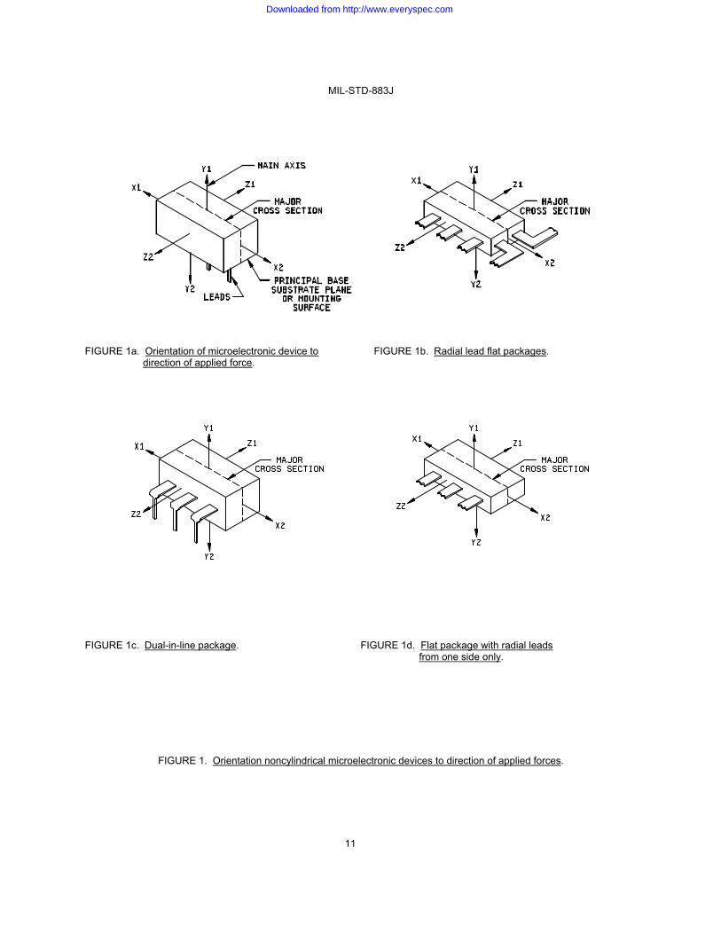
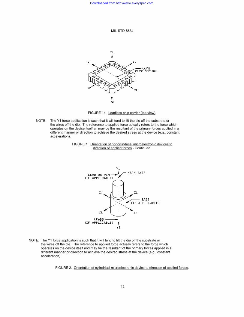
4.4 Orientation.
4.4.1 Identification of orientation and direction of forces applied. For those test methods which involve observation or the application of external forces which must be related to the orientation of the device, such orientation and direction of forces applied shall be identified in accordance with figures 1 and 2.
4.4.2 Orientation for other case configurations. For case configurations other than those shown in figures 1 and 2, the orientation of the device shall be as specified in the applicable acquisition document.
4.4.3 Orientation for packages with different size lateral dimensions. In flat packages where radial leads emanate from three or more sides, the X-direction shall be assigned to the larger and the Z-direction to the smaller of the two lateral dimensions.
Downloaded from http://www.everyspec.com
MIL-STD-883J
11
FIGURE 1a. Orientation of microelectronic device to FIGURE 1b. Radial lead flat packages. direction of applied force.
FIGURE 1c. Dual-in-line package. FIGURE 1d. Flat package with radial leads from one side only. FIGURE 1. Orientation noncylindrical microelectronic devices to direction of applied forces.
Downloaded from http://www.everyspec.com
MIL-STD-883J
12
FIGURE 1e. Leadless chip carrier (top view).
NOTE: The Y1 force application is such that it will tend to lift the die off the substrate or the wires off the die. The reference to applied force actually refers to the force which operates on the device itself an may be the resultant of the primary forces applied in a different manner or direction to achieve the desired stress at the device (e.g., constant acceleration).
FIGURE 1. Orientation of noncylindrical microelectronic devices to direction of applied forces - Continued.
NOTE: The Y1 force application is such that it will tend to lift the die off the substrate or the wires off the die. The reference to applied force actually refers to the force which operates on the device itself and may be the resultant of the primary forces applied in a different manner or direction to achieve the desired stress at the device (e.g., constant acceleration). FIGURE 2. Orientation of cylindrical microelectronic device to direction of applied forces.
Downloaded from http://www.everyspec.com
MIL-STD-883J
13
4.5 Test conditions. All newly designed device types shall meet the test conditions specified in 4.5.1 through 4.5.3.2. 4.5.1 Calibration requirements. Calibration shall be applied to those items of measuring and test equipment used to
assure product delivery specifications or critical manufacturing elements. Calibration shall be performed in accordance with the requirements of ANSI/NCSL Z540.3 or equivalent. Calibrated items shall be controlled, used and stored in a manner suitable to protect calibration integrity. Test equipment requiring calibration (single items or assemblages) shall be identified and labeled in accordance with ANSI/NCSL Z540.3 or equivalent.
4.5.2 Electrical test equipment accuracy. Unless otherwise specified in the acquisition document, test conditions such as:
voltage, resistive loads, capacitive loads, input switching parameters, input static parameters, currents and others shall be set to nominal values as defined in the acquisition document, with tolerances suitable for the test in which they are used.
4.5.3 Electrical test equipment capability. Using any or all of the following techniques, the manufacturer shall determine
that the test set/system is suitable to ensure product conformance with the acquisition document. Alternate suitable techniques may be used when approved by the qualifying activity. The manufacturer shall define and document methods used. The test equipment accuracy should be better than the allowable device tolerance in accordance with the following ratios:
a. Greater than or equal to 10:1 for routine processes. b. Greater than or equal to 4:1 for special processes (commercial equipment not readily available).
NOTE: State of the art requirements in which 4:1 can not be effectively achieved due to a lack of national standards shall be justified and documented.
4.5.3.1 Control based on uncertainty. Test processes that have complex characteristics are best performed and
controlled by the application of uncertainty analysis. The overall uncertainty in a test or measurement process shall be determined and the impact of said uncertainty on the product parameter tolerance shall be taken into account. The methods used for determining uncertainty shall be defined and documented. The method selected may use any (or combinations) of the following forms:
a. Arithmetic addition (linear), normally produces an overly conservative estimate and reflects a highly improbable
situation in which contributing errors are at their maximum limit at the same time and same direction. b. Root Sum Square (RSS), normally applied where the errors tend to fit a normal distribution (gaussian) and are from
independent sources. c. Partial Derivatives, used where complex relationships exist. d. Monte Carlo Simulation, used in very complex situations where other methods are not easily applied or do not fit. e. SRM (or controlled correlation device) testing providing observable data.
NOTE: Observable data, from a controlled device, may be relied upon to provide feedback that confirms process performance is within statistical limits.
f. Analysis of systematic and random errors, applying corrections as applicable. g. Any other recognized method of combining errors into an expression of uncertainty substantiated by an engineering
analysis. 4.5.3.2 Use and control of correlation devices/SRM's. When a manufacturer elects to use correlation devices or SRM's,
methods of use and control shall be in place and documented including parameters, type, quantity, description, identification, storage, handling and periodic verification requirements.
Downloaded from http://www.everyspec.com
MIL-STD-883J
14
4.5.4 Electrical test frequency. Unless otherwise specified, the electrical test frequency shall be the specified operating frequency. Where a frequency range is specified, major functional parameters shall be tested at the maximum and minimum frequencies of the range in addition to those tests conducted at any specified frequency within the range. Whenever electrical tests are conducted on microelectronic devices for which a range of frequencies or more than a single operating frequency is specified, the frequency at which tests are conducted shall be recorded along with the parameters measured at those frequencies.
4.5.5 Testing of multiple input/output devices. Where any input or output parameter is specified for devices having more
than a single input or output, the specified parameter shall be tested at all input or output terminations of the device. 4.5.6 Testing of complex devices. Where microelectronic devices being tested contain multiple circuits or functions,
whether independently connected to the external device leads or whether internally connected in some arrangement to minimize the number of external leads, suitable test circuits and procedures shall be applied so as to test all circuits or functions contained in the device with all the applicable test methods specified in the applicable acquisition document. For example, if a device contains a pair of logic gates it shall not be acceptable to test only one of the gates for the specified parameters. Furthermore, multiple circuit devices should be tested to assure that no significant interaction exists between individual circuits (e.g., application of signal to one gate of a dual gate device should not cause a change in output of the other gate). The intent of this requirement is to assure that all circuit elements in a microelectronic device are exercised to the fullest extent allowed by their construction and connection provisions. For circuit arrays containing complex signal paths which vary depending on the nature of incoming signals or internal functions performed on the incoming signals, this requirement shall be met by programming the operation of the device to assure that all circuit elements are caused to function and thus provide the opportunity to observe or measure the levels of their performance in accordance with the specified test methods.
4.5.7 Test environment. Unless otherwise specified herein, or in the applicable acquisition documentation, all
measurements and tests shall be made at ambient temperature of 25C +3C, -5C and at ambient atmospheric pressure from 580 to 800 millimeters mercury.
4.5.8 Permissible temperature variation in environmental chambers. When chambers are used, specimens under test
shall be located only within the working area defined as follows: a. Temperature variation within working area: The controls for the chamber shall be capable of maintaining the
temperature of any single reference point within the working area within ±2C or ±4 percent, whichever is greater. b. Space variation within working area: Chambers shall be so constructed that at any given time, the temperature of any
point within the working area shall not deviate more than ±3C or ±3 percent, whichever is greater, from the reference point, except for the immediate vicinity of specimens generating heat.
c. Chambers with specified minimum temperatures (e.g., burn-in, life test, etc.): When test requirements involve a
specified minimum test temperature, the controls and chamber construction shall be such that the temperature of any point within the working area shall not deviate more than +8C, -0C; or +8, -0 percent, whichever is greater, from the specified minimum temperature.
4.5.9 Control of test temperature during electrical measurements. Unless otherwise specified, the specified test
temperature, case (TC), ambient (TA), or junction (TJ) shall be controlled by the applicable procedure(s) specified herein. These are exclusively for the control of chambers, handlers, etc., used in electrical measurements of devices at specified temperatures and the provisions of 4.5.8 do not apply. Testing shall be conducted using either power-off condition followed by low duty cycle pulse testing or power stable temperature condition.
4.5.9.1 Temperature control during testing for TC, TA, or TJ above 25C. Unless otherwise specified, the device (including
its internal elements; e.g., die, capacitors, resistors, etc.) shall reach temperature and be stabilized in the power-off condition to within 3 C (or +6 C -3 C for hybrids) of the specified temperature. Note: Hybrids may exceed the positive tolerance of +6 C if their construction dictates and providing the manufacturer can assure that the devices under test are not degraded. When an established temperature characterization profile is available for a device to be tested, this profile may be used in lieu of temperature measurements to determine the proper heat soak conditions for meeting this requirement. When using a temperature characterization profile, test apparatus monitoring will assure that the controls are providing the proper test environment for that profile. After stabilization, testing shall be performed and the TC, TA, or TJ controlled to not fall more than 3 C from the specified temperature. The temperature during test may exceed 3 C of the specified TC, TA, or TJ provided the manufacturer assures that the devices under test are not being degraded. The electrical test parameters shall be measured using low duty cycle pulse testing or, if specified, power stable conditions (see 4.5.9.4).
Downloaded from http://www.everyspec.com
MIL-STD-883J
15
4.5.9.2 Temperature control during testing for TC, TA, or TJ below 25C. Unless otherwise specified, the device (including its internal elements; e.g., die, capacitors, resistors, etc.) shall reach temperature and be stabilized in the power-off condition to within +3 C (or –6 +3 C for hybrids) of the specified temperature (see note below). Note: Hybrids may exceed the negative tolerance of -6 C if their construction dictates and providing the manufacturer can assure that the devices under test are not degraded. When an established temperature characterization profile is available for a device to be tested, this profile may be used in lieu of temperature measurements to determine the proper heat soak conditions for meeting this requirement. When using a temperature characterization profile, test apparatus monitoring will assure that the controls are providing the proper test environment for that profile. After stabilization, (this temperature shall be identified as the cold-start temperature) testing shall be performed and the TC, TA, or TJ controlled to not exceed +5 C of the specified temperature throughout the test duration. The electrical test parameters shall be measured using low duty cycle pulse testing or, if specified, power stable conditions (see 4.5.9.4). When applicable, the detail specification shall specify those parameters or sequence of tests most sensitive to the cold-start temperature. These parameters, when specified, shall be measured at the start of the test sequence and shall be completed as soon as possible or within a specified time.
NOTE: Unless otherwise specified in the applicable detail specification, the set temperature shall be -55C (TC, TA, or TJ,
as applicable) or colder if the device temperature (TC, TA, or TJ, as applicable) increases by more than +5C during the test duration.
4.5.9.3 Temperature control during testing for TC, TA, or TJ at 25C. Unless otherwise specified, the device (including its
internal elements; e.g., die, capacitors, resistors, etc.) shall be stabilized in the power-off condition until the temperature is 25C +3C, -5C. The electrical test parameters shall be measured using low duty pulse testing or, if specified, power stable conditions (see 4.5.9.4).
4.5.9.4 Power stable temperature condition. When specified, the device shall be stabilized in the specified steady-state
power-on condition at the specified test temperature, TA, TC, or TJ as applicable, for temperatures at, above, or below 25C for a minimum time period of 5 minutes or a specified time. The electrical parameters measurements shall be completed as soon as possible or within a specified period of time after temperature/power stabilization has occurred. Alternatively, when specified, the device temperature TC or TA may be stabilized within 3C of the junction temperature typically predicted for the specified steady-state power-on condition of 5 minutes or more and the testing conducted with low duty pulse techniques.
4.6 General precautions. The following precautions shall be observed in the testing of devices: 4.6.1 Transients. Devices shall not be subjected to conditions in which voltage or current transients cause the ratings to
be exceeded. 4.6.2 Order of connection of leads. Care should be taken when connecting a microelectronic device to a power source.
For MOS devices or other microelectronic circuits or devices where the order of connection of leads may be important, precautions cited in the applicable acquisition document shall be observed.
4.6.3 Soldering and welding. Adequate precautions shall be taken to avoid damage to the device during soldering or
welding required for tests. 4.6.4 Radiation precautions. Due precautions shall be used in storing or testing microelectronic devices in substantial
fields of x-rays, neutrons, or other energy particles. 4.6.5 Handling precautions for microelectronic devices. a. Ground all equipment prior to insertion of the device for electrical test.
b. Where applicable, keep devices in metal shields until they are inserted in the equipment or until necessary to remove for test.
c. Where applicable, keep devices in carriers or other protective packages during test. 4.7 Recycled, recovered, or environmentally preferable materials. Recycled, recovered, or environmentally preferable
materials should be used to the maximum extent possible, provided that the material meets or exceeds the operational and maintenance requirements, and promotes economically advantageous life cycle costs.
Downloaded from http://www.everyspec.com
MIL-STD-883J
16
5. DETAILED REQUIREMENTS This section is not applicable to this standard.
Downloaded from http://www.everyspec.com
MIL-STD-883J
17
6. NOTES
(This section contains information of a general or explanatory nature that may be helpful, but is not mandatory.) 6.1 The intended use of this standard is to establish appropriate conditions for testing microcircuit devices to give test results that simulate the actual service conditions existing in the field. This standard has been prepared to provide uniform methods, controls, and procedures for determining with predictability the suitability of such devices within Military, Aerospace and special application equipment. This standard is applicable only to microelectronic devices, i.e. monolithic, multi-chip, film and hybrid microcircuits, microcircuit arrays, and the elements from which the circuits and arrays are formed. 6.2 Chemical listing. The following is a listing of chemicals identified for use in MIL-STD-883 test methods: Material CAS listing Test method Acetic Acid 64-19-7 2021 3.5-Dimethyl-1-hexyn-3-o1 4209-91-0 1002 Ethylbenzene 100-41-4 2015 Fluorescein 2321-07-5 1014 Freon-113 1/ 76-13-1 2015,1014 Hydrochloric Acid 7647-01-0 1009 Isopropyl Alcohol 67-63-0 2015,2003 Kerosene 8008-20-6 2015 Morpholine 110-91-8 1002 Methanol 67-56-1 1002 Methylene Chloride 1/ 75-09-2 2015 Mineral Spirits 8032-32-4 2015 Monoethanolamine 141-43-5 2015 Nitric Acid 7697-37-2 2021 Phosphoric Acid 7664-38-2 2021 Propylene Glycol Monomethyl Ether 107-98-2 2015 Rhodamine B 81-88-9 1014 Sodium Chloride 7647-14-5 1009,1002 Sodium Hydroxide 1310-73-2 1009 Stannous Chloride 7772-99-8 1002 1,1,1-Trichloroethane 1/ 71-55-6 2015 Zyglo Dye 8002-05-9 1014 In the event of a chemical emergency (example: spill, leak, fire, or exposure) obtain additional help or information by calling the telephone number listed below and identify the chemical by the CAS number provided above. Chem Trec: 1-800-424-9300 6.3 Subject term (key word) listing. Abbreviations Chemical listing Classification of tests Electrical test equipment accuracy General precautions Intended use Orientation Provisions for the use of MIL-STD-883 Test environment 1/ These chemicals are no longer required to be used in MIL-STD-883 test methods.
Downloaded from http://www.everyspec.com
MIL-STD-883J
18
6.4 Changes from previous issue. The margins of this standard are marked with asterisks where changes from the previous issue were made. This was done as a convenience only and the Government assumes no liability whatsoever for any inaccuracies in these notations. Bidders and contractors are cautioned to evaluate the requirements of this document based on the entire content irrespective of the marginal notations and relationship to the last previous issue.
Downloaded from http://www.everyspec.com
MIL-STD-883J
METHOD 1001 1 May 1968
1
METHOD 1001
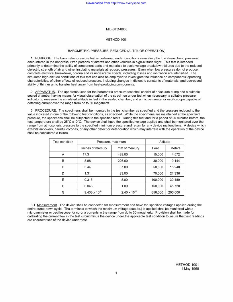
BAROMETRIC PRESSURE, REDUCED (ALTITUDE OPERATION) 1. PURPOSE. The barometric-pressure test is performed under conditions simulating the low atmospheric pressure encountered in the nonpressurized portions of aircraft and other vehicles in high-altitude flight. This test is intended primarily to determine the ability of component parts and materials to avoid voltage breakdown failures due to the reduced dielectric strength of air and other insulating materials at reduced pressures. Even when low pressures do not produce complete electrical breakdown, corona and its undesirable effects, including losses and ionization are intensified. The simulated high-altitude conditions of this test can also be employed to investigate the influence on components' operating characteristics, of other effects of reduced pressure, including changes in dielectric constants of materials, and decreased ability of thinner air to transfer heat away from heat-producing components. 2. APPARATUS. The apparatus used for the barometric-pressure test shall consist of a vacuum pump and a suitable sealed chamber having means for visual observation of the specimen under test when necessary, a suitable pressure indicator to measure the simulated altitude in feet in the sealed chamber, and a microammeter or oscilloscope capable of detecting current over the range from dc to 30 megahertz. 3. PROCEDURE. The specimens shall be mounted in the test chamber as specified and the pressure reduced to the value indicated in one of the following test conditions, as specified. While the specimens are maintained at the specified pressure, the specimens shall be subjected to the specified tests. During this test and for a period of 20 minutes before, the test temperature shall be 25°C ±10°C. The device shall have the specified voltage applied and shall be monitored over the range from atmospheric pressure to the specified minimum pressure and return for any device malfunctions. A device which exhibits arc-overs, harmful coronas, or any other defect or deterioration which may interfere with the operation of the device shall be considered a failure.
Test condition Pressure, maximum Altitude
Inches of mercury mm of mercury Feet Meters
A 17.3 439.00 15,000 4,572
B 8.88 226.00 30,000 9,144
C 3.44 87.00 50,000 15,240
D 1.31 33.00 70,000 21,336
E 0.315 8.00 100,000 30,480
F 0.043 1.09 150,000 45,720
G 9.436 x 10⁻⁸ 2.40 x 10⁻⁶ 656,000 200,000
3.1 Measurement. The device shall be connected for measurement and have the specified voltages applied during the entire pump-down cycle. The terminals to which the maximum voltage (see 4c.) is applied shall be monitored with a microammeter or oscilloscope for corona currents in the range from dc to 30 megahertz. Provision shall be made for calibrating the current flow in the test circuit minus the device under the applicable test condition to insure that test readings are characteristic of the device under test.
Downloaded from http://www.everyspec.com
MIL-STD-883J
METHOD 1001 1 May 1968 2
4. SUMMARY. The following details must be specified in the applicable acquisition document: a. Method of mounting (see 3). b. Test condition letter (see 3). Unless otherwise specified, condition E shall be used. c. Tests during subjection to reduced pressure (see 3). Unless otherwise specified, the device shall be subjected to
the maximum voltage it would be subjected to under rated operating conditions. d. Tests after subjection to reduced pressure, if applicable (see 3). Unless otherwise specified, the device shall be
subjected to full electrical tests of specified device characteristics or parameters. e. Exposure time prior to measurement, if applicable (see 3)
Downloaded from http://www.everyspec.com
MIL-STD-883J
METHOD 1002 1 May 1968
1
METHOD 1002 IMMERSION 1. PURPOSE. This test is performed to determine the effectiveness of the seal of microelectronic devices. The immersion of the part under evaluation into liquid at widely different temperatures subjects it to thermal and mechanical stresses which will readily detect a defective terminal assembly, or a partially closed seam or molded enclosure. Defects of these types can result from faulty construction or from mechanical damage such as might be produced during physical or environmental tests. The immersion test is generally performed immediately following such tests because it will tend to aggravate any incipient defects in seals, seams, and bushings which might otherwise escape notice. This test is essentially a laboratory test condition, and the procedure is intended only as a measurement of the effectiveness of the seal following this test. The choice of fresh or salt water as a test liquid is dependent on the nature of the component part under test. When electrical measurements are made after immersion cycling to obtain evidence of leakage through seals, the use of a salt solution instead of fresh water will facilitate detection of moisture penetration. This test provides a simple and ready means of detection of the migration of liquids. Effects noted can include lowered insulation resistance, corrosion of internal parts, and appearance of salt crystals. The test described is not intended as a thermal- shock or corrosion test, although it may incidentally reveal inadequacies in these respects. This is a destructive test and shall not be used as a 100 percent test or screen. 2. APPARATUS. The apparatus used for the immersion test shall consist of controlled temperature baths capable of maintaining the temperatures indicated for the hot bath and the cold bath test condition selected. A suitable temperature indicator shall be used to measure bath temperature. 3. PROCEDURE. This test consists of successive cycles of immersions, each cycle consisting of immersion in a hot bath of fresh (tap) water at a temperature of 65°C +5°C, -0°C followed by immersion in a cold bath. The number of cycles, duration of each immersion, and the nature and temperature of the cold bath shall be as indicated in the applicable test condition listed below, as specified. The transfer of specimens from one bath to another shall be accomplished as rapidly as practicable and in no case shall transfer time exceed 15 seconds. After completion of the final cycle, specimens shall be thoroughly and quickly washed in fresh (tap) water or distilled water and all surfaces wiped or air-blasted clean and dry. Unless otherwise specified, measurements shall be made at least 4 hours, but not more than 48 hours, after completion of the final cycle. When specified in the applicable acquisition document, upon completion of the electrical measurements and external visual examination, the device shall be delidded or dissected and examined in accordance with method 2013 for evidence of corrosion of internal elements or the appearance of salt crystals. Where this test is performed as part of a group or subgroup of tests, the post-test measurements or inspections need not be performed specifically at the conclusion of this test, but may be performed once at the conclusion of the group or subgroup.
Downloaded from http://www.everyspec.com
MIL-STD-883J
METHOD 1002 1 May 1968 2
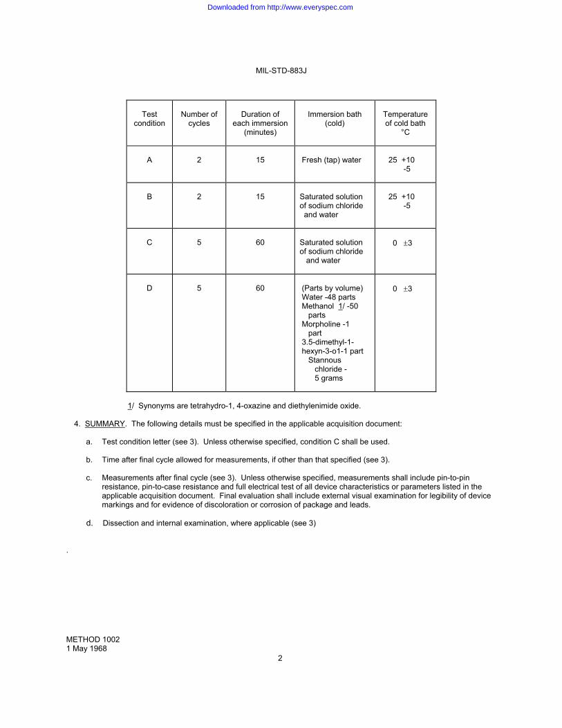
Test condition
Number of
cycles
Duration of
each immersion (minutes)
Immersion bath
(cold)
Temperature of cold bath
°C
A
2
15
Fresh (tap) water
25 +10 -5
B
2
15
Saturated solution of sodium chloride and water
25 +10 -5
C
5
60
Saturated solution of sodium chloride and water
0 3
D
5
60
(Parts by volume) Water -48 parts Methanol 1/ -50 parts Morpholine -1 part 3.5-dimethyl-1- hexyn-3-o1-1 part Stannous chloride - 5 grams
0 3
1/ Synonyms are tetrahydro-1, 4-oxazine and diethylenimide oxide. 4. SUMMARY. The following details must be specified in the applicable acquisition document: a. Test condition letter (see 3). Unless otherwise specified, condition C shall be used. b. Time after final cycle allowed for measurements, if other than that specified (see 3). c. Measurements after final cycle (see 3). Unless otherwise specified, measurements shall include pin-to-pin
resistance, pin-to-case resistance and full electrical test of all device characteristics or parameters listed in the applicable acquisition document. Final evaluation shall include external visual examination for legibility of device markings and for evidence of discoloration or corrosion of package and leads.
d. Dissection and internal examination, where applicable (see 3)
.
Downloaded from http://www.everyspec.com
MIL-STD-883J
METHOD 1003 1 May 1968
1
METHOD 1003 INSULATION RESISTANCE 1. PURPOSE. This test is to measure the resistance offered by the insulating members of a component part to an impressed direct voltage tending to produce a leakage of current through or on the surface of these members. Insulation- resistance measurements should not be considered the equivalent of dielectric withstanding voltage or electric breakdown tests. A clean, dry insulation may have a high insulation resistance, and yet possess a mechanical fault that would cause failure in the dielectric withstanding voltage test. Since insulating members composed of different materials or combinations of materials may have inherently different insulation resistances, the numerical value of measured insulation resistance cannot properly be taken as a direct measure of the degree of cleanliness or absence of deterioration. 1.1 Factors affecting use. Factors affecting insulation-resistance measurements include temperature, humidity, residual charges, charging currents or time constant of instrument and measured circuit, test voltage, previous conditioning, and duration of uninterrupted test voltage application (electrification time). In connection with this last-named factor, it is characteristic of certain components (for example, capacitors and cables) for the current to usually fall from an instantaneous high value to a steady lower value at a rate of decay which depends on such factors as test voltage, temperature, insulating materials, capacitance, and external circuit resistance. Consequently, the measured insulation resistance will increase for an appreciable time as test voltage is applied uninterruptedly. Because of this phenomenon, it may take many minutes to approach maximum insulation-resistance readings, but specifications usually require that readings be made after a specified time. This shortens the testing time considerably while still permitting significant test results, provided the insulation resistance is reasonably close to steady-state value, the current versus time curve is known, or suitable correction factors are applied to these measurements. For certain components, a steady instrument reading may be obtained in a matter of seconds. When insulation-resistance measurements are made before and after a test, both measurements should be made under the same conditions. 2. APPARATUS. Insulation-resistance measurements shall be made on an apparatus suitable for the characteristics of the component to be measured such as a megohm bridge, megohmmeter, insulation-resistance test set, or other suitable apparatus.
3. PROCEDURE. When special preparations or conditions such as special test fixtures, reconnections, grounding, isolation, low atmospheric pressure, humidity, or immersion in water are required, they shall be specified. Insulation- resistance measurements shall be made between the mutually insulated points or between insulated points and ground, as specified. When electrification time is a factor, the insulation-resistance measurements shall be made immediately after the specified time (see 4) of uninterrupted test voltage application, unless otherwise specified. However, if the instrument-reading indicates that an insulation resistance meets the specified limit, and is steady or increasing, the test may be terminated before the end of the specified period. When more than one measurement is specified, subsequent measurements of insulation resistance shall be made using the same polarity as the initial measurements. Unless otherwise specified, the direct potential applied to the specimen shall be that indicated by one of the test condition letters, as specified below, and insulation resistance measurements shall be made with both polarities of the applied voltage:
Test condition Test potential A 10 volts ±10% B 25 volts ±10% C 50 volts ±10% D 100 volts ±10% E 500 volts ±10% F 1,000 volts ±10% For inplant quality conformance testing, any voltage may be used provided it is equal to or greater than the minimum potential allowed by the applicable test condition. Unless otherwise specified, the measurement error at the insulation-resistance value shall not exceed 10 percent. Proper guarding techniques shall be used to prevent erroneous readings due to leakage along undesired paths.
Downloaded from http://www.everyspec.com
MIL-STD-883J
METHOD 1003 1 May 1968
2
4. SUMMARY. The following details must be specified in the applicable acquisition document: a. Test condition letter, or other test potential, if specified (see 3). b. Special preparations or conditions, if required (see 3). c. Points of measurement (see 3). Unless otherwise specified, insulation resistance shall be measured between the
device leads (all leads electrically connected to each other or to a common point) and the device case, and the measured resistance shall be no less than 15 megohms.
d. Electrification time, if critical (see 1.1). e. Insulation resistance in terms of maximum leakage current at a specified test voltage. Unless otherwise specified,
the maximum leakage between any adjacent disconnected leads shall not exceed 100 nanoampere at 100 volts dc.
Downloaded from http://www.everyspec.com
MIL-STD-883J
METHOD 1004.7 17 August 1987
1
METHOD 1004.7
MOISTURE RESISTANCE 1. PURPOSE. The moisture resistance test is performed for the purpose of evaluating, in an accelerated manner, the resistance of component parts and constituent materials to the deteriorative effects of the high-humidity and heat conditions typical of tropical environments. Most tropical degradation results directly or indirectly from absorption of moisture vapor and films by vulnerable insulating materials, and from surface wetting of metals and insulation. These phenomena produce many types of deterioration, including corrosion of metals; constituents of materials; and detrimental changes in electrical properties. This test differs from the steady-state humidity test and derives its added effectiveness in its employment of temperature cycling, which provides alternate periods of condensation and drying essential to the development of the corrosion processes and, in addition, produces a "breathing" action of moisture into partially sealed containers. Increased effectiveness is also obtained by use of a higher temperature, which intensifies the effects of humidity. The test includes a low-temperature subcycle that acts as an accelerant to reveal otherwise indiscernible evidences of deterioration since stresses caused by freezing moisture tend to widen cracks and fissures. As a result, the deterioration can be detected by the measurement of electrical characteristics (including such tests as voltage breakdown and insulation resistance) or by performance of a test for sealing. Provision is made for the application of a polarizing voltage across insulation to investigate the possibility of electrolysis, which can promote eventual dielectric breakdown. This test also provides for electrical loading of certain components, if desired, in order to determine the resistance of current-carrying components, especially fine wires and contacts, to electrochemical corrosion. Results obtained with this test are reproducible and have been confirmed by investigations of field failures. This test has proved reliable for indicating those parts which are unsuited for tropical field use. 2. APPARATUS. The apparatus used for the moisture resistance test shall include temperature-humidity chambers capable of maintaining the cycles and tolerance described on figure 1004-1 and electrical test equipment capable of performing the measurements in 3.6 and 4. 3. PROCEDURE. Specimens shall be tested in accordance with 3.2 through 3.7 inclusive, and figure 1004-1. Specimens shall be mounted in a manner that will expose them to the test environment. 3.1 Initial conditioning. Unless otherwise specified, prior to mounting specimens for the moisture resistance test, the device leads shall be subjected to a bending stress, initial conditioning in accordance with test condition B1 of method 2004. Where the specific sample devices being subjected to the moisture resistance test have already been subjected to the required initial conditioning, as part of another test employing the same sample devices, the lead bend need not be repeated. 3.2 Initial measurements. Prior to step 1 of the first cycle, the specified initial measurements shall be made at room ambient conditions, or as specified. When specified, the initial conditioning in a dry oven (see figure 1004-1) shall precede initial measurements and the initial measurements shall be completed within 8 hours after removal from the drying oven. 3.3 Number of cycles. Specimens shall be subjected to 10 continuous cycles, each as shown on figure 1004-1. In the event of no more than one unintentional test interruption (power interruption or equipment failure) prior to the completion of the specified number of cycles (except for the last cycle) the cycle shall be repeated and the test may continue. Unintentional interruptions occurring during the last cycle require a repeat of the cycle plus an additional uninterrupted cycle. Any intentional interruption, or any unintentional interruption of greater than 24 hours requires a complete retest.
Downloaded from http://www.everyspec.com
MIL-STD-883J
METHOD 1004.7 17 August 1987
2
3.4 Subcycle of step 7. During at least 5 of the 10 cycles a low temperature subcycle shall be performed. At least 1 hour but not more than 4 hours after step 7 begins, the specimens shall be either removed from the humidity chamber, or the temperature of the chamber shall be reduced, for performance of the subcycle. Specimens during the subcycle shall be conditioned at -10°C +2°C, -5°C, with humidity not controlled, for 3 hours minimum as indicated on figure 1004-1. When a separate cold chamber is not used, care should be taken to assure that the specimens are held at -10°C +2°C, -5°C, for the full period. After the subcycle, the specimens shall be returned to 25°C at 80 percent relative humidity (RH) minimum and kept there until the next cycle begins. 3.5 Applied voltage. During the moisture resistance test as specified on figure 1004-1, when specified (see 4), the device shall be biased in accordance with the specified bias configuration which should be chosen to maximize the voltage differential between chip metallization runs or external terminals, minimize power dissipation and to utilize as many terminals as possible to enhance test results. 3.6 Conditions (see figure 1004-1). The rate of change of temperature in the chamber is unspecified; however, specimens shall not be subject to the radiant heat from the chamber conditioning processes. The circulation of air in the chamber shall be at a minimum cubic rate per minute equivalent to five times the volume of the chamber unless otherwise specified. The steady-state temperature tolerance is ±2°C of the specified temperature at all points within the immediate vicinity of the specimens and at the chamber surfaces. Specimens weighing 25 pounds or less shall be transferred between temperature chambers in less than 2 minutes. 3.7 Final measurements. Following step 6 of the final cycle (or step 7 if the subcycle of 3.3 is performed during the tenth cycle), devices shall be conditioned for 24 hours at room ambient conditions after which either an insulation resistance test in accordance with method 1003, test condition A, or the specified 25°C electrical end-point measurements shall be performed. Electrical measurements may be made during the 24 hour conditioning period. However, any failures resulting from this testing shall be counted, and any retesting of these failures later in the 24 hour period for the purpose of obtaining an acceptable result is prohibited. No other test (e.g., seal) shall be performed during the 24 hour conditioning period. The insulation resistance test or the alternative 25°C electrical end-point measurements shall be completed within 48 hours after removing the devices from the chamber. When the insulation resistance test is performed, the measured resistance shall be no less than 10 megohms and the test shall be recorded and data submitted as part of the end-point data. If the package case is electrically connected to the die substrate by design, the insulation resistance test shall be omitted and the specified 25°C electrical end-point measurements shall be completed within 48 hours after removal of the device from the chamber. A visual examination and any other specified end-point electrical parameter measurements (see 4.c) shall also be performed. 3.8 Failure criteria. No device shall be acceptable that exhibits: a. Specified markings which are missing in whole or in part, faded, smeared, blurred, shifted, or dislodged to the
extent that they are not legible. This examination shall be conducted with normal room lighting and with a magnification of 1X to 3X.
b. Evidence of corrosion over more than 5 percent of the area of the finish or base metal of any package element
(i.e., lid, lead, or cap) or any corrosion that completely crosses the element when viewed with a magnification of 10X to 20X.
c. Leads missing, broken, or partially separated. d. Corrosion formations which bridge between leads or between leads and metal case. e. Electrical end-point or insulation resistance test failures.
NOTE: The finish shall include the package and entire exposed lead area from meniscus to the lead tip (excluding the
sheared off tip itself) and all other exposed metal surfaces.
Downloaded from http://www.everyspec.com
MIL-STD-883J
METHOD 1004.7 17 August 1987
3
4. SUMMARY. The following details shall be specified in the applicable acquisition document:
a. Initial measurements and conditions, if other than room ambient (see 3.1 and 3.2). b. Applied voltage, when applicable (see 3.5), and bias configuration, when required. This bias configuration shall
be chosen in accordance with the following guidelines: (1) Only one supply voltage (V) either positive or negative is required, and an electrical ground (GND) or
common terminal. The magnitude of V will be the maximum such that the specified absolute maximum ratings are not exceeded and test conditions are optimized.
(2) All normally specified voltage terminals and ground leads shall be connected to GND, unless otherwise
specified. (3) All data inputs, unless otherwise specified, shall be connected to V. The polarity and magnitude of V is
chosen to minimize internal power dissipation and current flow into the device. All extender inputs shall be connected to GND, unless otherwise specified.
(4) All additional leads, e.g., clock, set, reset, outputs, etc., considered individually, shall be connected to V or
GND whichever minimizes current flow. (5) Leads with no internal connection shall be biased to V or GND whichever is opposite to an adjacent lead. c. Final measurements (see 3.7). Final measurements shall include all electrical characteristics and parameters
which are specified as end-point electrical parameters. d. Number of cycles, if other than 10 (see 3.3). e. Conditioning in dry oven before initial measurements, if required (see 3.2).
Downloaded from http://www.everyspec.com
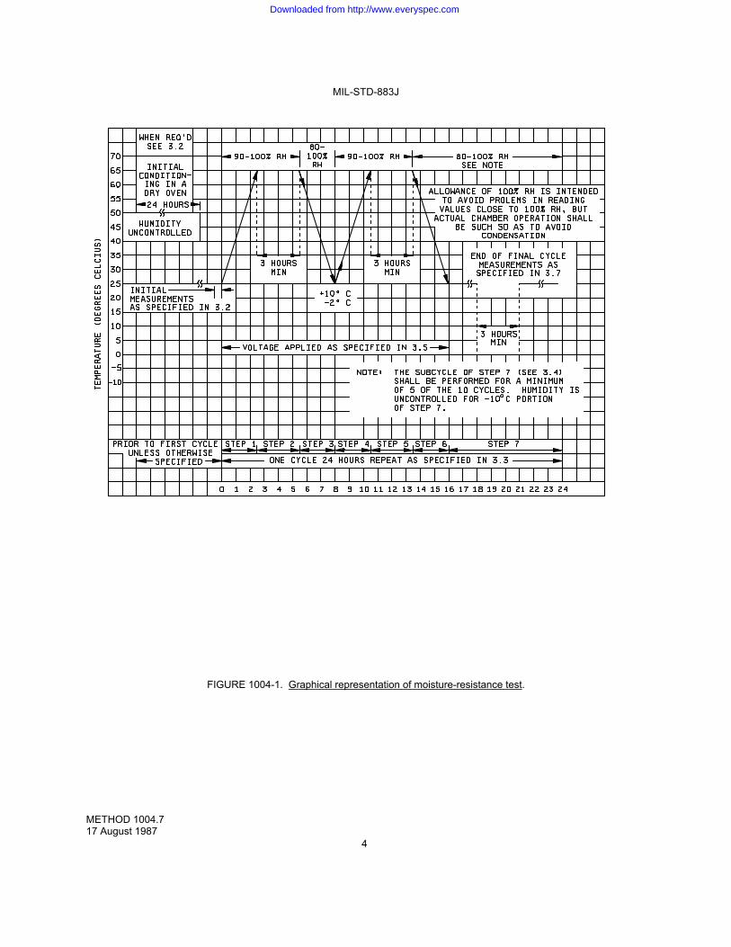
MIL-STD-883J
METHOD 1004.7 17 August 1987
4
FIGURE 1004-1. Graphical representation of moisture-resistance test.
Downloaded from http://www.everyspec.com
MIL-STD-883J
METHOD 1005.9 26 February 2010
1
METHOD 1005.9 STEADY-STATE LIFE
1. PURPOSE. The steady-state life test is performed for the purpose of demonstrating the quality or reliability of devices subjected to the specified conditions over an extended time period. Life tests conducted within rated operating conditions should be conducted for a sufficiently long test period to assure that results are not characteristic of early failures or "infant mortality," and periodic observations of results should be made prior to the end of the life test to provide an indication of any significant variation of failure rate with time. Valid results at shorter intervals or at lower stresses require accelerated test conditions or a sufficiently large sample size to provide a reasonable probability of detection of failures in the sample corresponding to the distribution of potential failures in the lot(s) from which the sample was drawn. The test conditions provided in 3 below are intended to reflect these considerations. When this test is employed for the purpose of assessing the general capability of a device or for device qualification tests in support of future device applications requiring high reliability, the test conditions should be selected so as to represent the maximum operating or testing (see test condition F) ratings of the device in terms of electrical input(s), load and bias and the corresponding maximum operating or testing temperature or other specified environment.
2. APPARATUS. Suitable sockets or other mounting means shall be provided to make firm electrical contact to the terminals of devices under test in the specified circuit configuration. Except as authorized by the acquiring or qualifying activity, the mounting means shall be so designated that they will not remove internally-dissipated heat from the device by conduction, other than that removed through the device terminals, the necessary electrical contacts and the gas or liquid chamber medium. The apparatus shall provide for maintaining the specified biases at the terminals of the device under test and, when specified, monitoring of the input excitation or output response. Power supplies and current-setting resistors shall be capable of maintaining the specified operating conditions as minimal throughout the testing period, despite normal variations in source voltages, ambient temperatures, etc. When test conditions result in significant power dissipation, the test apparatus shall be arranged so as to result in the approximate average power dissipation for each device whether devices are tested individually or in a group. The test circuits need not compensate for normal variations in individual device characteristics, but shall be so arranged that the existence of failed or abnormal (i.e., open, short, etc.) devices in a group does not negate the effect of the test for other devices in the group.
3. PROCEDURE. The microelectronic devices shall be subjected to the specified test condition (see 3.5) for the specified duration at the specified test temperature, and the required measurements shall be made at the specified intermediate points and end points. QML manufactures who are certified and qualified to MIL-PRF-38535 may modify the time or the condition independently from the regression conditions contained in table I or the test condition/circuit specified in the device specification or standard microcircuit drawing provided the modification is contained in the manufacturer's QM plan and the "Q" certification identifier is marked on the devices. Lead-, stud-, or case-mounted devices shall be mounted by the leads, stud, or case in their normal mounting configuration, and the point of connection shall be maintained at a temperature not less than the specified ambient temperature. The test condition, duration, sample size, and temperature selected prior to test shall be recorded and shall govern for the entire test. Test boards shall not employ load resistors which are common to more than one device, or to more than one output pin on the same device.
3.1 Test duration.
3.1.1 Test duration - standard life. The life test duration shall be 1,000 hours minimum at 125°C , unless otherwise specified or allowed (see 3.2.1). After the specified duration of the test, the device shall be removed from the test conditions and allowed to reach standard test conditions. Where the purpose of this test is to demonstrate compliance with a specified lambda (8), the test may be terminated at the specified duration or at the point of rejection if this occurs prior to the specified test duration.
Downloaded from http://www.everyspec.com
MIL-STD-883J
METHOD 1005.9 26 February 2010
2
3.1.2 Accelerated life test duration. For class level B, the life test duration, when accelerated, shall be the time equivalent to 1,000 hours at 125°C for the ambient temperature selected or specified (see table I). Within 72 hours after the specified duration of the test, the device shall be removed from the specified test conditions and allowed to reach standard test conditions without removal of bias. The interruption of bias for up to one minute for the purpose of moving the devices to cool-down positions separate from the chamber within which life testing was performed shall not be considered removal of bias.
3.2 Test temperature. The specified test temperature is the minimum ambient temperature to which all devices in the working area of the chamber shall be exposed. This shall be assured by making whatever adjustments are necessary in the chamber profile, loading, location of control or monitoring instruments, and the flow of air or other suitable gas or liquid chamber medium. Therefore, calibration shall be accomplished in the chamber in a fully loaded, (boards need not be loaded with devices) unpowered configuration, and the indicator sensor located at, or adjusted to reflect, the coldest point in the working area.
3.2.1 Test temperature - standard life. Unless otherwise specified, the ambient life test temperature shall be 125°C minimum for test conditions A through E (see 3.5), except that for hybrid microcircuits, the conditions may be modified in accordance with table I. At the supplier's option, the ambient temperature for conditions A through E may be increased and the test duration reduced in accordance with table I using the specified test circuit and bias conditions. Since case and junction temperature will, under normal circumstances, be significantly higher than ambient temperature, the circuit should be so structured that maximum rated case or junction temperatures for test or operation shall not exceed 200°C for class level B or 175°C for class level S (see 3.2.1.1).
3.2.1.1 Test temperature for high power devices. Regardless of power level, devices shall be able to be burned in or life-tested at their maximum rated operating temperature. For devices whose maximum operating temperature is stated in terms of ambient temperature, TA, table I applies. For devices whose maximum operating temperature is stated in terms of case temperature, TC, and where the ambient temperature would cause TJ to exceed +200°C (+175°C for class level S), the ambient operating temperature may be reduced during burn-in and life test from +125°C to a value that will demonstrate a TJ between +175°C and +200°C and TC equal to or greater than +125°C without changing the test duration. Data supporting this reduction shall be available to the acquiring and qualifying activities upon request.
3.2.1.2 Test temperature for hybrid devices. The ambient or case life test temperature shall be as specified in table I,
except case temperature life test shall be performed, as a minimum, at the maximum operating case temperature (TC) specified for the device. Life test shall be for 1,000 hours minimum for class level S hybrid (class K). The device should be life tested at the maximum specified operating temperature, voltage, and loading conditions as specified in the detail specification. Since case and junction temperature will, under normal circumstances, be significantly higher than ambient temperature, the circuit should be so structured that the maximum rated junction temperature as specified in the device specification or drawing and the cure temperature of polymeric materials as specified in the baseline documentation shall not be exceeded. If no maximum junction temperature is specified, a maximum of 175°C is assumed. Accelerated life test (condition F) shall not be permitted. The specified test temperature shall be the minimum actual ambient or case temperature that must be maintained for all devices in the chamber. This shall be assured by making whatever adjustments are necessary in the chamber profile, loading, location of control or monitoring instruments and the flow of air or other suitable gas or liquid chamber medium.
3.2.2 Test temperature - accelerated life. When condition F is specified or is utilized as an option (when allowed by the applicable acquisition documents), the minimum ambient test temperature shall be +175°C , unless otherwise specified. Since accelerated testing will normally be performed at temperatures higher than the maximum rated operating junction temperature of the device(s) tested, care shall be taken to ensure that the device(s) does not go into thermal runaway. 3.2.3 Special considerations for devices with internal thermal limitation using test conditions A through E. For devices with internal thermal shutdown, extended exposure at a temperature in excess of the shut-down temperature will not provide a realistic indicator of long-term operating reliability. For devices equipped with thermal shutdown, operating life test shall be performed at an ambient temperature where the worst case junction temperature is at least 5°C below the worst case thermal shutdown threshold. Data supporting the defined thermal shutdown threshold shall be available to the preparing or acquiring activity upon request.
Downloaded from http://www.everyspec.com
MIL-STD-883J
METHOD 1005.9 26 February 2010
3
3.3 Measurements.
3.3.1 Measurements for test temperatures less than or equal to 150°C . Unless otherwise specified, all specified
intermediate and end-point measurements shall be completed within 96 hours after removal of the device from the specified test conditions (i.e., either removal of temperature or bias). If these measurements cannot be completed within 96 hours, the devices shall be subjected to the same test condition (see 3.5) and temperature previously used for a minimum of 24 additional hours before intermediate or end-point measurements are made. When specified (or at the manufacturer's discretion, if not specified), intermediate measurements shall be made at 168 (+72, -0) hours and at 504 (+168, -0) hours. For tests in excess of 1,000 hours duration, additional intermediate measurement points, when specified, shall be 1000 (+168, -24) hours, 2,000 (+168, -24) hours, and each succeeding 1,000 (+168, -24) hour interval. These intermediate measurements shall consist of the parameters and conditions specified, including major functional characteristics of the device under test, sufficient to reveal both catastrophic and degradation failures to specified limits. Devices shall be cooled to less than 10°C of their power stable condition at room temperature prior to the removal of bias. The interruption of bias for up to one minute for the purpose of moving the devices to cool-down positions separate from the chamber within which life testing was performed shall not be considered removal of bias. Alternatively, except for linear or MOS (CMOS, NMOS, PMOS, etc.) devices or unless otherwise specified, the bias may be removed during cooling, provided the case temperature of the devices under test is reduced to a maximum of 35°C within 30 minutes after removal of the test conditions and provided the devices under test are removed from the heated chamber within five minutes following removal of bias. All specified 25°C electrical measurements shall be completed prior to any reheating of the device(s).
3.3.2 Measurements for test temperatures greater than or equal to 175°C . Unless otherwise specified, all specified intermediate and end-point measurements shall be completed within 24 hours after removal of the device from the specified test conditions (i.e., either removal of temperature or bias). If these measurements cannot be completed within 24 hours, the steady-state life test shall be repeated using the same test condition, temperature and time. Devices shall be cooled to less than 10°C of their power stable condition at room temperature prior to the removal of bias, except that the interruption of bias for up to one minute for the purpose of moving the devices to cool-down positions shall not be considered removal of bias. All specified 25°C electrical measurements shall be completed prior to any reheating of the device(s).
3.3.3 Test setup monitoring. The test setup shall be monitored at the test temperature initially and at the conclusion of the test to establish that all devices are being stressed to the specified requirements. The following is the minimum acceptable monitoring procedure: a. Device sockets. Initially and at least each 6 months thereafter, (once every 6 months or just prior to use if not
used during the 6 month period) each test board or tray shall be checked to verify continuity to connector points to assure that bias supplies and signal information will be applied to each socket. Board capacitance or resistance required to ensure stability of devices under test shall be checked during these initial and periodic verification tests to ensure they will perform their proper function (i.e., that they are not open or shorted). Except for this initial and periodic verification, each device or device socket does not have to be checked; however, random sampling techniques shall be applied prior to each time a board is used and shall be adequate to assure that there are correct and continuous electrical connections to the devices under test.
b. Connectors to test boards or trays. After the test boards are loaded with devices, inserted into the oven, and
brought up to at least 125°C or the specified test temperature, whichever is less, each required test voltage and signal condition shall be verified in at least one location on each test board or tray so as to assure electrical continuity and the correct application of specified electrical stresses for each connection or contact pair used in the applicable test configuration. This may be performed by opening the oven for a maximum of 10 minutes. When the test conditions are checked at a test socket, contact points on the instrument used to make this continuity check shall be equal to or smaller dimensions than the leads (contacts) of the devices to be tested and shall be constructed such that the socket contacts are not disfigured or damaged.
c. At the conclusion of the test period, prior to removal of devices from temperature and test conditions, the voltage
and signal condition verification of b. above shall be repeated.
d. For class level S devices, each test board or tray and each test socket shall be verified prior to test to assure that the specified test conditions are applied to each device. This may be accomplished by verifying the device functional response at each device output(s). An approved alternate procedure may be used.
Where failures or open contacts occur which result in removal of the required test stresses for any period of the required test duration (see 3.1), the test time shall be extended to assure actual exposure for the total minimum specified test duration. Any loss(es) or interruption(s) of bias in excess of 10 minutes total duration whether or not the chamber is at temperature during the final 24 hours of life test shall require extension of the test duration for an uninterrupted 24 hours minimum, after the last bias interruption.
Downloaded from http://www.everyspec.com
MIL-STD-883J
METHOD 1005.9 26 February 2010
4
3.4 Test sample. The test sample shall be as specified (see 4). When this test method is employed as an add-on life test
for a series or family of device types, lesser quantities of any single device type may be introduced in any single addition to the total sample quantity, but the results shall not be considered valid until the minimum sample size for each device has been accumulated. Where all or part of the samples previously under test are extracted upon addition of new samples, the minimum sample size for each type shall be maintained once that level is initially reached and no sample shall be extracted until it has accumulated the specified minimum test hours (see 3.1).
3.5 Test conditions.
3.5.1 Test condition A, steady-state, reverse bias. This condition is illustrated on figure 1005-1 and is suitable for use on all types of circuits, both linear and digital. In this test, as many junctions as possible will be reverse biased to the specified voltage.
3.5.2 Test condition B, steady-state, forward bias. This test condition is illustrated on figure 1005-1 and can be used on all digital type circuits and some linear types. In this test, as many junctions as possible will be forward biased as specified.
3.5.3 Test condition C, steady-state, power and reverse bias. This condition is illustrated on figure 1005-1 and can be used on all digital type circuits and some linear types where the inputs can be reverse biased and the output can be biased for maximum power dissipation or vice versa.
3.5.4 Test condition D, parallel excitation. This test condition is typically illustrated on figure 1005-2 and is suitable for use on all circuit types. All circuits must be driven with an appropriate signal to simulate, as closely as possible, circuit application and all circuits shall have maximum load applied. The excitation frequency shall not be less than 60 Hz.
3.5.5 Test condition E, ring oscillator. This test condition is illustrated on figure 1005-3, with the output of the last circuit normally connected to the input of the first circuit. The series will be free running at a frequency established by the propagation delay of each circuit and associated wiring and the frequency shall not be less than 60 Hz. In the case of circuits which cause phase inversion, an odd number of circuits shall be used. Each circuit in the ring shall be loaded to its rated maximum. While this condition affords the opportunity to continuously monitor the test for catastrophic failures (i.e., ring stoppage), this shall not be considered acceptable as a substitute for the intermediate measurements (see 3.3).
3.5.6 Test condition F, (class level B only) temperature-accelerated test. In this test condition, microcircuits are subjected to bias(es) at an ambient test temperature (175°C to 300°C ) which considerably exceeds their maximum rated temperature. At higher temperatures, it is generally found that microcircuits will not operate normally, and it is therefore necessary that special attention be given to the choice of bias circuits and conditions to assure that important circuit areas are adequately biased without damaging overstresses to other areas of the circuit. To properly select the actual biasing conditions to be used, it is recommended that an adequate sample of devices be exposed to the intended high temperature while measuring voltage(s) and current(s) at each device terminal to assure that the specified circuit and the applied electrical stresses do not induce damaging overstresses.
At the manufacturer's option, alternate time and temperature values may be established from table I. Any time-temperature
combination which is contained in table I within the time limit of 30 to 1,000 hours may be used. The life test ground rules of 3.5 of method 1016 shall apply to life tests conducted using test condition F. The applied voltage at any or all terminals shall be equal to the voltage specified for the 125°C operating life in the applicable acquisition document, unless otherwise specified. If necessary, with the specific approval of the qualifying activity, the applied voltage at any or all terminal(s) may be reduced to not less than 50 percent of the specified value(s) when it is demonstrated that excessive current flow or power dissipation would result from operation at the specified voltage(s). If the voltage(s) is so reduced, the life test duration shall be determined by the following formula: to (100%) Ta = 100% - V% Where Ta is the adjusted total test duration in hours, to is the original test duration in hours, and V percent is the largest percentage of voltage reduction made in any specified voltage.
Downloaded from http://www.everyspec.com
MIL-STD-883J
METHOD 1005.9 26 February 2010
5
3.5.6.1 Special considerations for devices with internal thermal limitation. For devices with internal thermal shutdown,
extended exposure at a temperature in excess of the shut-down temperature will not provide a realistic indicator of long-term operating reliability. For such devices, measurement of the case temperature should be made at the specified bias voltages at several different ambient temperatures. From these measurements, junction temperatures should be computed, and the operating life shall be performed at that ambient temperature which, with the voltage biases specified, will result in a worst case junction temperature at least 5°C but no more than 10°C below the minimum junction temperature at which the device would go into thermal shutdown, and the test time shall be determined from table I for the applicable device class level.
4. SUMMARY. The following details shall be specified in the applicable acquisition document:
a. Special preconditioning, when applicable.
b. Test temperature, and whether ambient, junction, or case, if other than as specified in 3.2.
c. Test duration, if other than as specified in 3.1.
d. Test mounting, if other than normal (see 3). e. Test condition letter.
f. End-point measurements and intermediate measurements (see 3.3).
g. Criteria for device failure for intermediate and end-point measurements (see 3.3), if other than device specification limits, and criteria for lot acceptance.
h. Test sample (see 3.4).
i. Time to complete end-point measurements, if other than as specified (see 3.3).
j. Authorization for use of condition F and special maximum test rating for condition F, when applicable (see 4.b).
k. Time temperature conditions for condition F, if other than as specified in 3.5.6.
Downloaded from http://www.everyspec.com
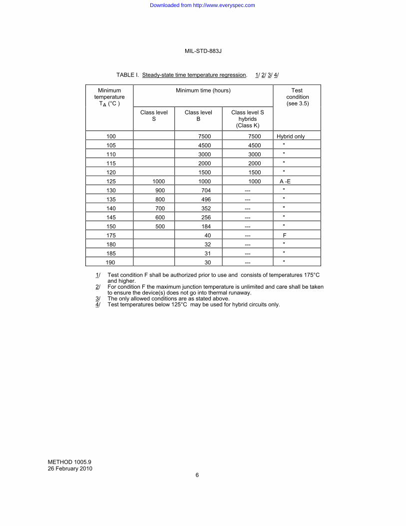
MIL-STD-883J
METHOD 1005.9 26 February 2010
6
TABLE I. Steady-state time temperature regression. 1/ 2/ 3/ 4/
Minimum temperature
TA (°C )
Minimum time (hours) Test condition (see 3.5)
Class level S
Class level B
Class level S hybrids
(Class K)
100 7500 7500 Hybrid only
105 4500 4500 "
110 3000 3000 "
115 2000 2000 "
120 1500 1500 "
125 1000 1000 1000 A -E
130 900 704 --- "
135 800 496 --- "
140 700 352 --- "
145 600 256 --- "
150 500 184 --- "
175 40 --- F
180 32 --- "
185 31 --- "
190 30 --- "
1/ Test condition F shall be authorized prior to use and consists of temperatures 175°C and higher.
2/ For condition F the maximum junction temperature is unlimited and care shall be taken to ensure the device(s) does not go into thermal runaway.
3/ The only allowed conditions are as stated above. 4/ Test temperatures below 125°C may be used for hybrid circuits only.
Downloaded from http://www.everyspec.com
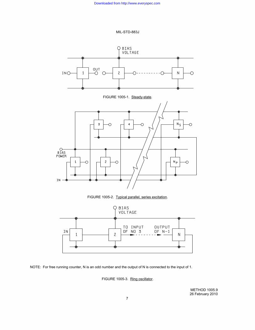
MIL-STD-883J
METHOD 1005.9 26 February 2010
7
FIGURE 1005-1. Steady-state.
FIGURE 1005-2. Typical parallel, series excitation.
NOTE: For free running counter, N is an odd number and the output of N is connected to the input of 1. FIGURE 1005-3. Ring oscillator.
Downloaded from http://www.everyspec.com
MIL-STD-883J
METHOD 1005.9 26 February 2010
8
This page intentionally left blank
Downloaded from http://www.everyspec.com
MIL-STD-883J
METHOD 1006 1 May 1968
1
METHOD 1006 INTERMITTENT LIFE 1. PURPOSE. The intermittent life test is performed for the purpose of determining a representative failure rate for microelectronic devices or demonstrating quality or reliability of devices subjected to the specified conditions. It is intended for applications where the devices are exposed to cyclic variations in electrical stresses between the "on" and "off" condition and resultant cyclic variations in device and case temperatures. 2. APPARATUS. See method 1005 of this standard. 3. PROCEDURE. The device shall be tested in accordance with all the requirements of method 1005 except that all electrical stresses shall be alternately applied and removed. The "on" and "off" periods shall be initiated by sudden, not gradual, application or removal of the specified electrical inputs (including signal and bias). 4. SUMMARY. In addition to the requirements of method 1005 of this standard, the following detail shall be specified in the applicable acquisition document: Frequency and duration of "on" and "off" cycles
Downloaded from http://www.everyspec.com

MIL-STD-883J
METHOD 1006 1 May 1968
2
This page intentionally left blank .
Downloaded from http://www.everyspec.com
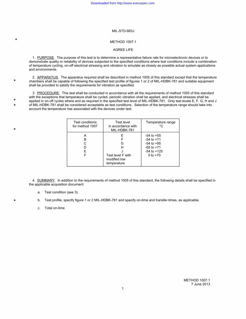
MIL-STD-883J
METHOD 1007.1 7 June 2013
1
METHOD 1007.1 AGREE LIFE 1. PURPOSE. The purpose of this test is to determine a representative failure rate for microelectronic devices or to demonstrate quality or reliability of devices subjected to the specified conditions where test conditions include a combination of temperature cycling, on-off electrical stressing and vibration to simulate as closely as possible actual system applications and environments. 2. APPARATUS. The apparatus required shall be described in method 1005 of this standard except that the temperature chambers shall be capable of following the specified test profile of figures 1 or 2 of MIL-HDBK-781 and suitable equipment shall be provided to satisfy the requirements for vibration as specified. 3. PROCEDURE. This test shall be conducted in accordance with all the requirements of method 1005 of this standard with the exceptions that temperature shall be cycled, periodic vibration shall be applied, and electrical stresses shall be applied in on-off cycles where and as required in the specified test level of MIL-HDBK-781. Only test levels E, F, G, H and J of MIL-HDBK-781 shall be considered acceptable as test conditions. Selection of the temperature range should take into account the temperature rise associated with the devices under test.
Test conditions for method 1007
Test level in accordance with
MIL-HDBK-781
Temperature range °C
A E -54 to +55 B F -54 to +71 C G -54 to +95 D H -65 to +71 E J -54 to +125 F Test level F with
modified low temperature
0 to +70
4. SUMMARY. In addition to the requirements of method 1005 of this standard, the following details shall be specified in the applicable acquisition document: a. Test condition (see 3). b. Test profile, specify figure 1 or 2 MIL-HDBK-781 and specify on-time and transfer-times, as applicable. c. Total on-time
*
**
*
*
*
Downloaded from http://www.everyspec.com

MIL-STD-883J
METHOD 1007.1 7 June 2015
2
This page intentionally left blank
Downloaded from http://www.everyspec.com
MIL-STD-883J
METHOD 1008.2 25 August 1993
1
METHOD 1008.2 STABILIZATION BAKE 1. PURPOSE. The purpose of this test is to determine the effect on microelectronic devices of storage at elevated temperatures without electrical stress applied. This method may also be used in a screening sequence or as a preconditioning treatment prior to the conduct of other tests. This test shall not be used to determine device failure rates for other than storage conditions. It may be desirable to make end point and, where applicable, intermediate measurements on a serialized device basis or on the basis of a histogram distribution by total sample in order to increase the sensitivity of the test to parameter degradation or the progression of specific failure mechanisms with time and temperature. 2. APPARATUS. The apparatus required for this test shall consist of a controlled temperature chamber capable of maintaining the specified temperature and suitable electrical equipment to make the specified end point measurements. 3. PROCEDURE. The device shall be stored at the specified ambient conditions for the specified time. The time at high temperature shall be sufficient to allow the total mass of each device under test to reach the specified temperature before the specified time duration begins. Within the time interval of 24 hours before (0 hours before test durations less than 250 hours) to 72 hours after the specified duration of the test, the device shall be removed from the specified ambient test condition and allowed to reach standard test conditions. When specified, end-point measurements shall be completed within 96 hours after removal of device from the specified ambient test condition. When specified (or at the manufacturer's discretion, if not specified) intermediate measurements shall be made at intermediate points. 3.1 Test condition. The ambient test temperature shall be indicated by specifying a test condition letter from the following table. The specified test temperature is the minimum actual ambient temperature to which all devices in the working area of the chamber are exposed. This shall be assured by making whatever adjustments are necessary in the chamber profile, loading, location of control or monitoring instruments, and the flow of air or other chamber atmosphere. Therefore, calibration, shall be accomplished on the chamber in a fully, loaded, unpowered configuration, and the indicator sensor located at, or adjusted to reflect, the coldest point in the working area. Unless otherwise specified, test condition C minimum, with a minimum time duration and temperature as specified in table I, shall apply. Unless otherwise specified, the test duration for all other test conditions shall be 24 hours minimum. Test condition Temperature (minimum) A 75°C B 125°C C See table I D 200°C E 250°C F 300°C G 350°C H 400°C
Downloaded from http://www.everyspec.com
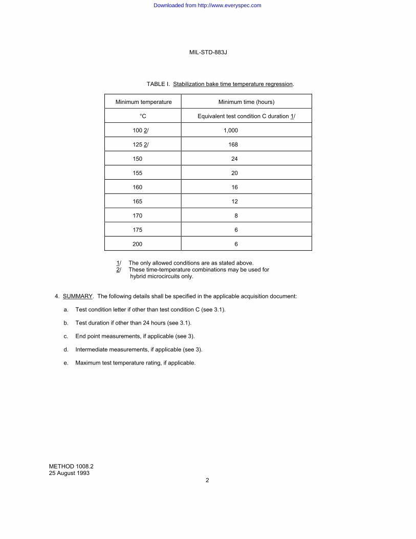
MIL-STD-883J
METHOD 1008.2 25 August 1993
2
TABLE I. Stabilization bake time temperature regression.
Minimum temperature Minimum time (hours)
°C Equivalent test condition C duration 1/
100 2/ 1,000
125 2/ 168
150 24
155 20
160 16
165 12
170 8
175 6
200 6
1/ The only allowed conditions are as stated above. 2/ These time-temperature combinations may be used for hybrid microcircuits only. 4. SUMMARY. The following details shall be specified in the applicable acquisition document: a. Test condition letter if other than test condition C (see 3.1). b. Test duration if other than 24 hours (see 3.1). c. End point measurements, if applicable (see 3). d. Intermediate measurements, if applicable (see 3). e. Maximum test temperature rating, if applicable.
Downloaded from http://www.everyspec.com
MIL-STD-883J
METHOD 1009.8 22 March 1989
1
METHOD 1009.8 SALT ATMOSPHERE (CORROSION) 1. PURPOSE. This test is proposed as an accelerated laboratory corrosion test simulating the effects of seacoast atmosphere on devices and package elements. 1.1 Terms and definitions. 1.1.1 Corrosion. Corrosion is the deterioration of coating or base metal or both by chemical or electrochemical action. 1.1.2 Corrosion site. A corrosion site is the site at which the coating or base metal or both is corroded. The location of corrosion. 1.1.3 Corrosion product (deposit). The effect of corrosion (i.e., rust or iron oxide, nickel oxide, tin oxide, etc.). The product of corrosion may be at the corrosion site, or may flow or run (due to action of liquid carrier of salt) so as to cover noncorroded areas. 1.1.4 Corrosion stain. Corrosion stain is a semitransparent deposit due to corrosion products. 1.1.5 Blister. A blister is a localized swelling and separation between the coating(s) and base metal. 1.1.6 Pinhole. A pinhole is a small hole occurring in the coating as an imperfection which penetrates entirely through the coating. 1.1.7 Pitting. Pitting is the localized corrosion of coating or base metal or both, confined to a point or small area, that takes the form of cavities. 1.1.8 Flaking. Flaking is the separation of small pieces of coating that exposes the base metal. 2. APPARATUS. Apparatus used in the salt-atmosphere test shall include the following: a. Exposure chamber with fixtures for supporting devices. The chamber and all accessories shall be made of
material (glass, plastic, etc.) which will not affect the corrosiveness of the salt atmosphere. All parts within the test chamber which come in contact with test specimens shall be of materials that will not cause electrolytic corrosion. The chamber shall be properly vented to prevent pressure build-up and allow uniform distribution of salt fog.
b. Salt solution reservoir adequately protected from the surrounding ambient. If necessary, auxiliary reservoirs may
be used for long duration tests in accordance with test conditions C and D (see 3.2). c. Means for atomizing the salt solution, including suitable nozzles and compressed air or a 20 percent oxygen, 80
percent nitrogen mixture (the gas entering the atomizers shall be free from all impurities such as oil and dirt). d. Chamber-heating means and controls. e. Means for humidifying the air at temperature above the chamber temperature. f. Air or inert gas dryer.
g. Magnifier(s) 1X to 3X, 10X to 20X and 30X to 60X.
Downloaded from http://www.everyspec.com
MIL-STD-883J
METHOD 1009.8 22 March 1989
2
3. PROCEDURE. 3.1 Maintenance and conditioning of test chamber. The purpose of the cleaning cycle is to assure that all materials which could adversely affect the results of the subsequent tests are removed from the chamber. The chamber shall be cleaned by operating it at 95°F ±5°F (35°C ±3°C) with deionized or distilled water as long as necessary. The chamber shall be cleaned each time the salt solution in the reservoir has been used up. Several test runs therefore could be run before cleaning, depending on the size of the reservoir and the specified test condition (see 3.2). When long duration conditions (test conditions C and D, see 3.2) are required, the reservoir may be refilled via auxiliary reservoirs so that the test cycle shall not be interrupted. After the cleaning cycle, on restarting the chamber, the reservoir shall be filled with salt solution and the chamber shall be stabilized by operating it until the temperature comes to equilibrium, see 3.1.4. If operation of the chamber is discontinued for more than one week, the remaining salt solution, if any, shall be discarded. Cleaning shall then be performed prior to restarting the test chamber. Intermittent operation of the chamber is acceptable provided the pH and concentration of the salt solution are kept within limits defined in 3.1.1. 3.1.1 Salt solution. The salt concentration shall be 0.5 to 3.0 percent by weight in deionized or distilled water as required to achieve the deposition rates required by 3.1.4. The salt used shall be sodium chloride containing on the dry basis not more than 0.1 percent by weight of sodium iodide and not more than 0.3 percent by weight total impurities. The pH of the salt solution shall be maintained between 6.5 and 7.2 when measured at 95°F ±5°F (35°C ±3°C). Only CP grade (dilute solution) hydrochloric acid or sodium hydroxide shall be used to adjust the pH. 3.1.2 Preconditioning of leads. Unless otherwise specified, the test specimens shall not be preconditioned. If required (see 4.c.), prior to mounting specimens for the salt atmosphere test, the device leads shall be subjected to the bending stress initial conditioning in accordance with test condition B1 of method 2004. Where the specific sample devices being subjected to the salt atmosphere test have already been subjected to the required initial conditioning, as part of another test employing the same sample devices, the lead bend need not be repeated. 3.1.3 Mounting of test specimens. The test specimens shall be mounted on the holding fixtures (plexiglass rods, nylon or fiberglass screens, nylon cords, etc.) in accordance with the applicable orientation(s) below. Specimens shall also be positioned so that they do not contact each other, so that they do not shield each other from the freely settling fog, and so that corrosion products and condensate from one specimen does not fall on another. a. Dual-in-line packages with leads attached to, or exiting from, package sides (such as side-brazed packages and
ceramic dual-in-line packages): Lid upward 15° to 45° from vertical. One of the package sides on which the leads are located shall be oriented upward at an angle greater than or equal to 15° from vertical (see figure 1009-1a).
b. Packages with leads attached to, or exiting from the opposite side of the lid (such as TO cans, solid sidewall
packages, and metal platform packages): Lid 15° to 45° from vertical. One-half of the samples shall be tested with the lid upward; the remaining samples shall be tested with the leads upward (see figure 1009-1b). For packages with leads attached to, or exiting from the same side as the lid, only one orientation (lid and leads upward) is required.
c. Packages with leads attached to, or exiting from package sides, parallel to the lid (such as flatpacks): Lid 15° to
45° from vertical. One of the package sides on which the leads are located shall be oriented upward at an angle greater than or equal to 15° from vertical. For packages with a metal case, one-half of the samples shall be tested with the lid upward; the remaining samples shall be tested with the case upward. All other packages shall be tested with the lid upward (see figure 1009-1c).
d. Leadless and leaded chip carriers: Lid 15° to 45° from vertical. One-half of the samples shall be tested with the lid
upward; the remaining samples shall be tested with the lid downward (see figure 1009-1d). e. Flat specimens (e.g., lids only and lead frames only): 15° to 45° from vertical.
Downloaded from http://www.everyspec.com
MIL-STD-883J
METHOD 1009.8 22 March 1989
3
NOTE: In cases where two orientations are required for testing, the specified sample size shall be divided in half (or as
close to one-half as possible). In all cases, inspections following the test in accordance with 3.4 shall be performed on all package surfaces.
NOTE: Precautions may be used to prevent light induced photovoltaic electrolytic effects when testing windowed UV
erasable devices. 3.1.4 Chamber operation. After conditioning of test chamber in accordance with 3, a salt fog having a temperature of 95°F minimum (35°C minimum) shall be passed through the chamber for the specified test duration (see 3.2). The exposure zone of the chamber shall be maintained at a temperature of 95°F ±5°F (35°C ±3°C). The fog concentration and velocity shall be so adjusted that the rate of salt deposit in the test area is between 20,000 and 50,000 mg/m2/24 hours. Rate of salt deposit may be determined by either volumetric, gravimetric, or other techniques at the user's option. The salt solution collecting at the bottom of the chamber shall be discarded. 3.2 Length of test. The minimum duration of exposure of the salt atmosphere test shall be specified by indicating a test condition letter from the following table. Unless otherwise specified, test condition A shall apply: Test condition Length of test A 24 hours B 48 hours C 96 hours D 240 hours 3.3 Preparation of specimens for examination. Upon completion of the salt exposure test, the test specimens shall be immediately washed with free flowing deionized water (not warmer than 100°F (38°C) for at least 5 minutes to remove salt deposits from their surface after which they shall be dried with air or inert gas, and subjected to the inspections below. 3.4 Failure criteria. All inspections shall be performed at a magnification of 10X to 20X, unless otherwise specified in this procedure (see 3.4.1b and 3.4.1c). NOTES: 1. Corrosion stains shall not be considered as part of the defective area of 3.4.1a. 2. Corrosion products resulting from lead corrosion that deposit onto areas other than the lead shall not be
considered as part of the defective area of 3.4.1a. 3. Corrosion at the tips of the leads and corrosion products resulting from such corrosion shall be disregarded. 4. Portions of leads which cannot be further tested in accordance with 3.4.1b, due to geometry or design (such as
standoffs on pin grid arrays or the brazed portion of leads on side-brazed packages), shall be subject to the failure criteria of 3.4.1a.
3.4.1 Finished product. No device is acceptable that exhibits: a. Corrosion defects over more than 5 percent of the area of the finish or base metal of any package element other
than leads such as lid, cap, or case. Corrosion defects to be included in this measurement are: Pitting, blistering, flaking, and corrosion products. The defective area may be determined by: Comparison with charts or photographs of known defective areas (see figure 1009-2), direct measurement using a grid or similar measuring device, or image analysis.
Downloaded from http://www.everyspec.com
MIL-STD-883J
METHOD 1009.8 22 March 1989
4
b. Leads missing, broken, or partially separated. In addition, any lead which exhibits pinholes, pitting, blistering,
flaking, corrosion product that completely crosses the lead, or any evidence of pinholes, pitting, blistering, flaking, corrosion product, or corrosion stain at the glass seal shall be further tested as follows:
Bend the lead through 90° at the point of degradation in such a manner that tensile stress is applied to the
defect region. Any lead which breaks or shows fracture of the base metal through greater than 50 percent of the cross-sectional area of the lead shall be considered a reject. In the case of multiple defects the bend shall be made at the site exhibiting the worst case corrosion. On packages exhibiting defects on more than ten leads, bends shall be made on a maximum of ten leads exhibiting the worst case corrosion. The examination of the fracture shall be performed with a magnification of 30X to 60X.
c. Specified markings, which are missing in whole or in part, faded, smeared, blurred, shifted, or dislodged to the
extent that they are not legible. This examination shall be conducted with normal room lighting and with a magnification of 1X to 3X.
3.4.2 Package elements. When this test is performed on package elements or partially assembled packages during incoming inspection or any time prior to completion of package assembly as an optional quality control gate or as a required test (see 4.d), no part is acceptable that exhibits: a. Corrosion defects over more than 1.0 percent of the area of the finish or base metal of lids or over more than 2.5
percent of the area of the finish or base metal of any other package element other than leads (such as case). Corrosion on areas of the finish or base metal that will not be exposed to surrounding ambient after device fabrication shall be disregarded. This inspection shall be performed according to the procedure in 3.4.1a.
b. Leads with final lead finish that are rejectable in accordance with 3.4.1b. 4. SUMMARY. The following details shall be specified in the applicable acquisition document: a. Test duration, if other than test condition A (see 3.2). b. Measurements and examinations after test, when applicable for other than visual (see 3.4). c. Requirement for preconditioning, if applicable, and procedure if other than in 3.1.2. d. Requirement for incoming inspection of package elements or partially assembled packages (see 3.4.2), when
applicable.
Downloaded from http://www.everyspec.com
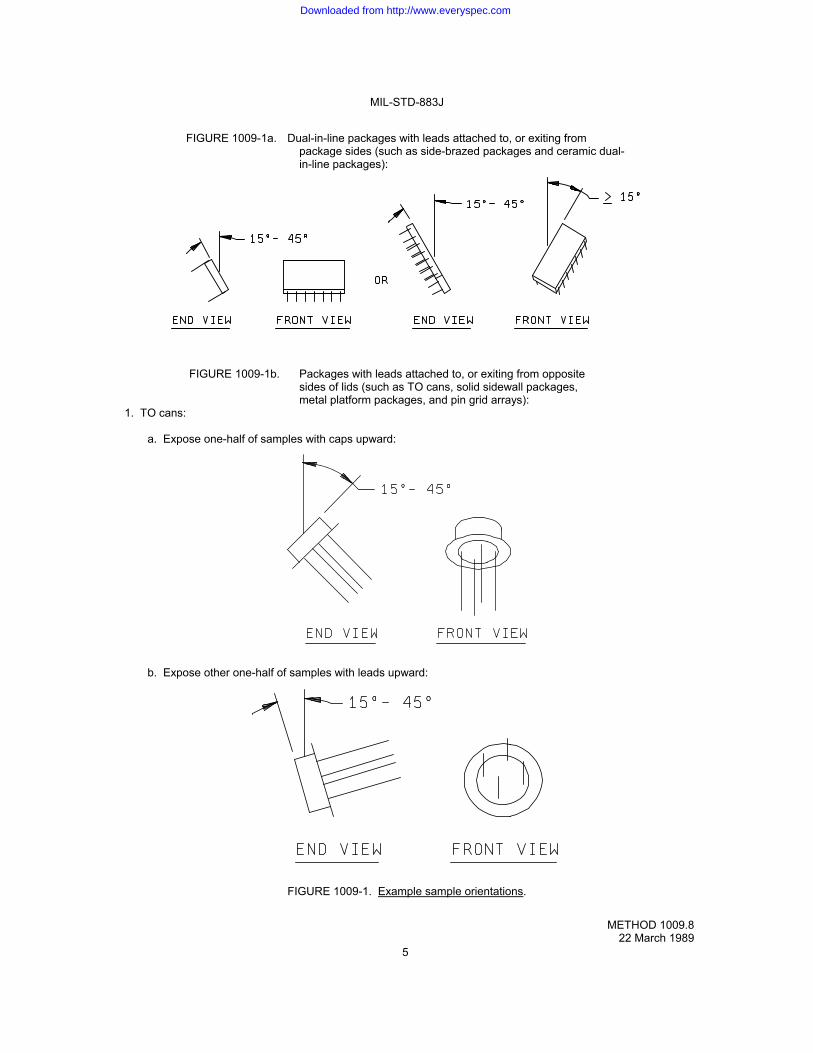
MIL-STD-883J
METHOD 1009.8 22 March 1989
5
FIGURE 1009-1a. Dual-in-line packages with leads attached to, or exiting from package sides (such as side-brazed packages and ceramic dual- in-line packages):
FIGURE 1009-1b. Packages with leads attached to, or exiting from opposite sides of lids (such as TO cans, solid sidewall packages, metal platform packages, and pin grid arrays): 1. TO cans: a. Expose one-half of samples with caps upward:
b. Expose other one-half of samples with leads upward:
FIGURE 1009-1. Example sample orientations.
Downloaded from http://www.everyspec.com
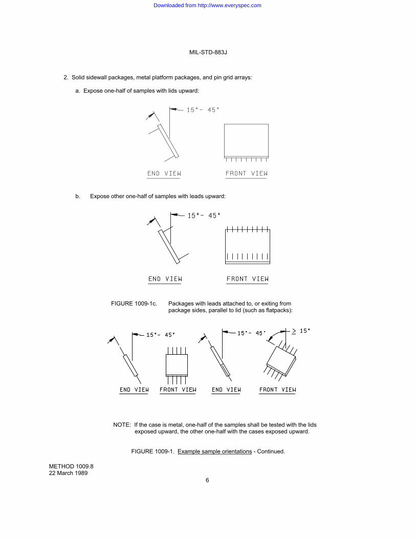
MIL-STD-883J
METHOD 1009.8 22 March 1989
6
2. Solid sidewall packages, metal platform packages, and pin grid arrays: a. Expose one-half of samples with lids upward:
b. Expose other one-half of samples with leads upward:
FIGURE 1009-1c. Packages with leads attached to, or exiting from package sides, parallel to lid (such as flatpacks):
NOTE: If the case is metal, one-half of the samples shall be tested with the lids exposed upward, the other one-half with the cases exposed upward.
FIGURE 1009-1. Example sample orientations - Continued.
Downloaded from http://www.everyspec.com
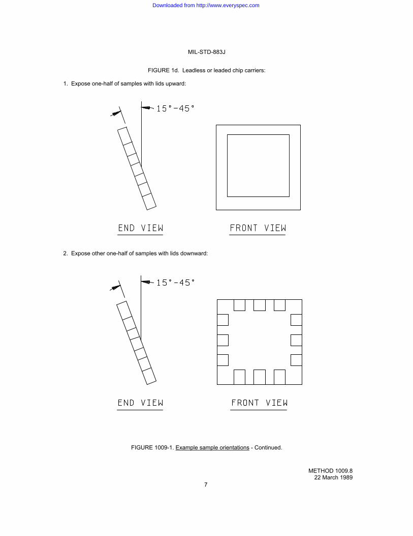
MIL-STD-883J
METHOD 1009.8 22 March 1989
7
FIGURE 1d. Leadless or leaded chip carriers: 1. Expose one-half of samples with lids upward:
2. Expose other one-half of samples with lids downward:
FIGURE 1009-1. Example sample orientations - Continued.
Downloaded from http://www.everyspec.com
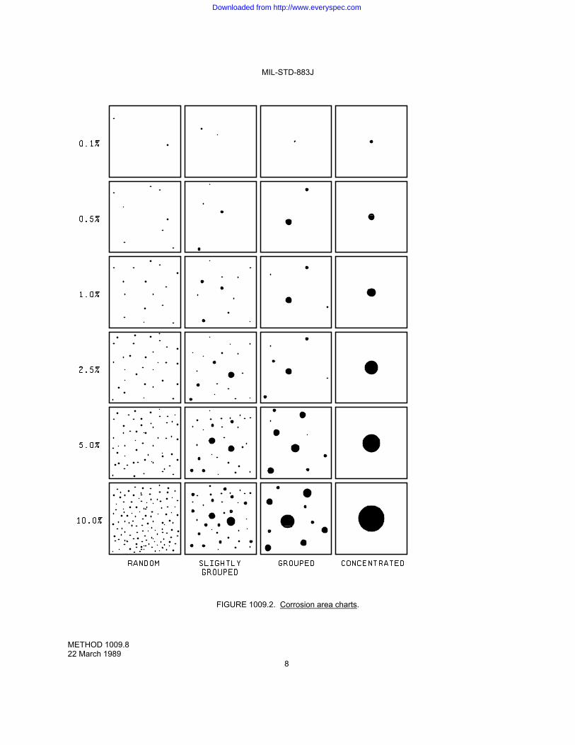
MIL-STD-883J
METHOD 1009.8 22 March 1989
8
FIGURE 1009.2. Corrosion area charts.
Downloaded from http://www.everyspec.com
MIL-STD-883J
METHOD 1010.8 18 June 2004
1
METHOD 1010.8
TEMPERATURE CYCLING 1. PURPOSE. This test is conducted to determine the resistance of a part to extremes of high and low temperatures, and to the effect of alternate exposures to these extremes. 1.1 Terms and definitions. 1.1.1 Load. The specimens under test and the fixtures holding those specimens during the test. Maximum load shall be determined by using the worst case load temperature with specific specimen loading. Monolithic (single block) loads used to simulate loading may not be appropriate when air circulation is reduced by load configuration. The maximum loading must meet the specified conditions. 1.1.2 Monitoring sensor. The temperature sensor that is located to indicate the same temperature as that of the worst case indicator specimen location. The worst case indicator specimen location is identified during the periodic characterization of the worst case load temperature. 1.1.3 Worst case load temperature. The temperature of specific specimens or equivalent mass as indicated by thermocouples imbedded in their bodies. These indictor specimens shall be located at the center and at each corner of the load. The worst case load temperature (point which reaches temperature last) is determined at periodic intervals. 1.1.4 Working zone. The volume in the chamber(s) in which the temperature of the load is controlled within the limits specified in table I. 1.1.5 Specimen. The device or individual piece being tested. 1.1.6 Transfer time. The elapsed time between initiation of load transition (for a single chamber or specimen removal for multiple chambers) from one temperature extreme and introduction into the other temperature. 1.1.7 Maximum load. The largest load for which the worst case load temperature meets the timing requirements. 1.1.8 Dwell time. The time from introduction of the load to one extreme environment temperature until the initiation of the transfer to the other extreme temperature environment. 2. APPARATUS. The chamber(s) used shall be capable of providing and controlling the specified temperatures in the working zone(s) when the chamber is loaded with a maximum load. The thermal capacity and air circulation must enable the working zone and loads to meet the specified conditions and timing (see 3.1). Worst case load temperature shall be continually monitored during test by indicators or recorders. Direct heat conduction to specimens shall be minimized. 3. PROCEDURE. Specimens shall be placed in such a position with respect to the airstream that there is substantially no obstruction to the flow of air across and around the specimen. When special mounting is required, it shall be specified. The specimen shall then be subjected to the specified condition for the specified number of cycles performed continuously. This test shall be conducted for a minimum of 10 cycles using test condition C (see Figure 1010-1). One cycle consists of steps 1 and 2 or the applicable test condition and must be completed without interruption to be counted as a cycle. Completion of the total number of cycles specified for the test may be interrupted for the purpose of test chamber loading or unloading of device lots or as the result of power or equipment failure. However, if the number of interruptions for any reason exceeds 10 percent of the total number of cycles specified, the test must be restarted from the beginning. 3.1 Timing. The total transfer time from hot to cold or from cold to hot shall not exceed one minute (for multiple chambers). The load may be transferred when the worst case load temperature is within the limits specified in table I. However, the dwell time shall not be less than 10 minutes and the load shall reach the specified temperature within 15 minutes (16 minutes for single chamber).
Downloaded from http://www.everyspec.com
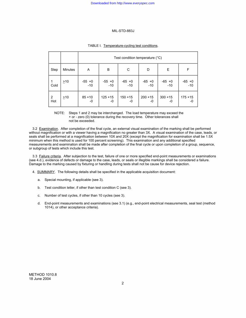
MIL-STD-883J
METHOD 1010.8 18 June 2004
2
TABLE I. Temperature-cycling test conditions.
Test condition temperature (°C)
Step
Minutes
A
B
C
D
E
F
1 Cold
>10
-55 +0 -10
-55 +0 -10
-65 +0 -10
-65 +0 -10
-65 +0 -10
-65 +0 -10
2 Hot
>10
85 +10 -0
125 +15 -0
150 +15 -0
200 +15 -0
300 +15 -0
175 +15 -0
NOTE: Steps 1 and 2 may be interchanged. The load temperature may exceed the + or - zero (0) tolerance during the recovery time. Other tolerances shall not be exceeded.
3.2 Examination. After completion of the final cycle, an external visual examination of the marking shall be performed without magnification or with a viewer having a magnification no greater than 3X. A visual examination of the case, leads, or seals shall be performed at a magnification between 10X and 20X (except the magnification for examination shall be 1.5X minimum when this method is used for 100 percent screening). This examination and any additional specified measurements and examination shall be made after completion of the final cycle or upon completion of a group, sequence, or subgroup of tests which include this test. 3.3 Failure criteria. After subjection to the test, failure of one or more specified end-point measurements or examinations (see 4.d.), evidence of defects or damage to the case, leads, or seals or illegible markings shall be considered a failure. Damage to the marking caused by fixturing or handling during tests shall not be cause for device rejection. 4. SUMMARY. The following details shall be specified in the applicable acquisition document: a. Special mounting, if applicable (see 3). b. Test condition letter, if other than test condition C (see 3). c. Number of test cycles, if other than 10 cycles (see 3). d. End-point measurements and examinations (see 3.1) (e.g., end-point electrical measurements, seal test (method
1014), or other acceptance criteria).
Downloaded from http://www.everyspec.com
MIL-STD-883J
METHOD 1010.8 18 June 2004
3
Figure 1010-1 An example of Temperature Cycling Test Condition C.
Downloaded from http://www.everyspec.com
MIL-STD-883J
METHOD 1010.8 18 June 2004
4
This page intentionally left blank
Downloaded from http://www.everyspec.com
MIL-STD-883J
METHOD 1011.9 27 July 1990
1
METHOD 1011.9 THERMAL SHOCK 1. PURPOSE. The purpose of this test is to determine the resistance of the part to sudden exposure to extreme changes in temperature and the effect of alternate exposures to these extremes. 1.1 Terms and definitions. 1.1.1 Cycle. A cycle consists of starting at ambient room temperature, proceeding to step 1, then to step 2, or alternately proceeding to step 2, then to step 1, and then back to ambient room temperature without interruption. 1.1.2 Dwell time. The total time the load is immersed in the bath. 1.1.3 Load. The devices under test and the fixture holding these devices. 1.1.4 Maximum load. The maximum mass of devices and fixtures that can be placed in the bath while maintaining specified temperatures and times. 1.1.5 Specimen. The device or individual piece being tested. 1.1.6 Transfer time. The elapsed time measured from removal of the load from one bath until insertion in the other bath. 1.1.7 Worst case load temperature. The body temperature of a specific device located at the center of the load. 1.1.8 Monitoring sensor. The temperature sensor that is located and calibrated so as to indicate the same temperature as at the worst case indicator specimen location. The worst case indicator specimen location is identified during the periodic characterization of the worst case load temperature. 2. APPARATUS. The baths used shall be capable of providing and controlling the specified temperatures in the working zone(s) when the bath is loaded with a maximum load. The thermal capacity and liquid circulation must enable the working zone and loads to meet the specified conditions and timing (see 3.1). Worst case load temperature shall be continually monitored during test by indicators or recorders reading the monitoring sensor(s). The worst case load temperature under maximum load conditions and configuration shall be verified as needed to validate bath performance. Perfluorocarbons that meet the physical property requirements of table II shall be used for conditions B and C. 3. PROCEDURE. Specimens shall be placed in the bath in a position so that the flow of liquid across and around them is substantially unobstructed. The load shall then be subjected to condition B or as otherwise specified (see 4b) of table I for a duration of 15 cycles. Completion of the total number of cycles specified for the test may be interrupted for the purpose of loading or unloading of device lots or as the result of power or equipment failure. However, if the number of interruptions for any given test exceeds 10 percent of the total number of cycles specified, the test must be restarted from the beginning. 3.1 Timing. The total transfer time from hot to cold or from cold to hot shall not exceed 10 seconds. The load may be transferred when the worst case load temperature is within the limits specified in table I. However, the dwell time shall be not less than 2 minutes and the load shall reach the specified temperature within 5 minutes.
Downloaded from http://www.everyspec.com
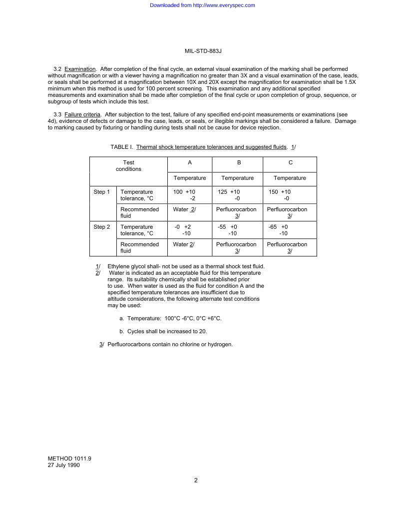
MIL-STD-883J
METHOD 1011.9 27 July 1990
2
3.2 Examination. After completion of the final cycle, an external visual examination of the marking shall be performed without magnification or with a viewer having a magnification no greater than 3X and a visual examination of the case, leads, or seals shall be performed at a magnification between 10X and 20X except the magnification for examination shall be 1.5X minimum when this method is used for 100 percent screening. This examination and any additional specified measurements and examination shall be made after completion of the final cycle or upon completion of group, sequence, or subgroup of tests which include this test. 3.3 Failure criteria. After subjection to the test, failure of any specified end-point measurements or examinations (see 4d), evidence of defects or damage to the case, leads, or seals, or illegible markings shall be considered a failure. Damage to marking caused by fixturing or handling during tests shall not be cause for device rejection.
TABLE I. Thermal shock temperature tolerances and suggested fluids. 1/
Test conditions
A B C
Temperature Temperature Temperature
Step 1 Temperature tolerance, °C
100 +10 -2
125 +10 -0
150 +10 -0
Recommended fluid
Water 2/ Perfluorocarbon 3/
Perfluorocarbon 3/
Step 2 Temperature tolerance, °C
-0 +2 -10
-55 +0 -10
-65 +0 -10
Recommended fluid
Water 2/ Perfluorocarbon 3/
Perfluorocarbon 3/
1/ Ethylene glycol shall- not be used as a thermal shock test fluid. 2/ Water is indicated as an acceptable fluid for this temperature range. Its suitability chemically shall be established prior to use. When water is used as the fluid for condition A and the specified temperature tolerances are insufficient due to altitude considerations, the following alternate test conditions may be used:
a. Temperature: 100°C -6°C, 0°C +6°C. b. Cycles shall be increased to 20. 3/ Perfluorocarbons contain no chlorine or hydrogen.
Downloaded from http://www.everyspec.com
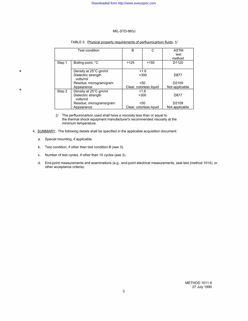
MIL-STD-883J
METHOD 1011.9 27 July 1990
3
TABLE II. Physical property requirements of perfluorocarbon fluids. 1/
Test condition B C
ASTM test
method Step 1 Boiling point, °C >125 >150 D1120
Density at 25°C gm/ml Dielectric strength volts/mil Residue, microgram/gram Appearance
>1.6 >300
<50
Clear, colorless liquid
D877
D2109
Not applicable Step 2 Density at 25°C gm/ml
Dielectric strength volts/mil Residue, micrograms/gram Appearance
>1.6 >300
<50
Clear, colorless liquid
D877
D2109
Not applicable 1/ The perfluorocarbon used shall have a viscosity less than or equal to the thermal shock equipment manufacturer's recommended viscosity at the minimum temperature. 4. SUMMARY. The following details shall be specified in the applicable acquisition document: a. Special mounting, if applicable. b. Test condition, if other than test condition B (see 3). c. Number of test cycles, if other than 15 cycles (see 3). d. End-point measurements and examinations (e.g., end-point electrical measurements, seal test (method 1014), or
other acceptance criteria).
*
*
Downloaded from http://www.everyspec.com
MIL-STD-883J
METHOD 1011.9 27 July 1990
4
This page intentionally left blank
Downloaded from http://www.everyspec.com
MIL-STD-883J
METHOD 1012.1 4 November 1980
1
METHOD 1012.1
THERMAL CHARACTERISTICS 1. PURPOSE. The purpose of this test is to determine the thermal characteristics of microelectronic devices. This includes junction temperature, thermal resistance, case and mounting temperature and thermal response time of the microelectronic devices. 1.1 Definitions. The following definitions and symbols shall apply for the purpose of this test: a. Case temperature, TC, in °C. The case temperature is the temperature at a specified accessible reference point
on the package in which the microelectronic chip is mounted. b. Mounting surface temperature, TM, in °C. The mounting surface temperature is the temperature of a specified
point at the device-heat sink mounting interface (or primary heat removal surface). c. Junction temperature, TJ, in °C. The term is used to denote the temperature of the semiconductor junction in the
microcircuit in which the major part of the heat is generated. With respect to junction temperature measurements, TJ(Peak) is the peak temperature of an operating junction element in which the current distribution is nonuniform, TJ(Avg) is the average temperature of an operating junction element in which the current distribution is nonuniform, and TJ(Region) is the temperature in the immediate vicinity within six equivalent radii (an equivalent radius is the radius of a circle having the same area as contained in a junction interface area) of an operating junction. In general TJ(Region) <TJ(Avg) <TJ(Peak). If the current distribution in an operating junction element is uniform then TJ(Avg) < TJ(Peak).
d. Thermal resistance, junction to specified reference point, RJR, in °C/W. The thermal resistance of the microcircuit
is the temperature difference from the junction to some reference point on the package divided by the power dissipation PD.
e. Power dissipation, PD, in watts, is the power dissipated in a single semiconductor test junction or in the total
package, PD(Package). f. Thermal response time, tJR, in seconds, is the time required to reach 90 percent of the final value of junction
temperature change caused by the application of a step function in power dissipation when the device reference point temperature is held constant. The thermal response time is specified as tJR(Peak), tJR(Avg), or tJR(Region) to conform to the particular approach used to measure the junction temperature.
g. Temperature sensitive parameter, TSP, is the temperature dependent electrical characteristic of the
junction-under test which can be calibrated with respect to temperature and subsequently used to detect the junction temperature of interest.
2. APPARATUS. The apparatus required for these tests shall include the following as applicable to the specified test procedures. a. Thermocouple material shall be copper-constantan (type T) or equivalent, for the temperature range -180°C to
+370°C. The wire size shall be no larger than AWG size 30. The junction of the thermocouple shall be welded to form a bead rather than soldered or twisted. The accuracy of the thermocouple and associated measuring system shall be ±0.5°C.
b. Controlled temperature chamber or heat sink capable of maintaining the specified reference point temperature to
within ±0.5°C of the preset (measured) value.
Downloaded from http://www.everyspec.com
MIL-STD-883J
METHOD 1012.1 4 November 1980
2
c. Suitable electrical equipment as required to provide controlled levels of conditioning power and to make the
specified measurements. The instrument used to electrically measure the temperature-sensitive parameter shall be capable of resolving a voltage change of 0.5 mV. An appropriate sample-and-hold unit or a cathode ray oscilloscope shall be used for this purpose.
d. Infrared microradiometer capable of measuring radiation in the 1 to 6 micrometer range and having the ability to
detect radiation emitted from an area having a spatial resolution of less than 40 micrometers (1.6 mils) diameter at its half power points and a temperature resolution (detectable temperature change) of 0.5°C at 60°C.
NOTE: May be a scanning IR microradiometer.
e. A typical heat sink assembly for mounting the microelectronic device-under test is shown on figure 1012-1. The
primary heat sink is water cooled and has a thermocouple sensor for inlet and outlet water temperature as shown in Figure 1012-1.
An adapter heat sink, as shown on Figure 1012-1 is fastened to the top surface of the primary heat sink, and has a special geometry to handle specific size packages, e.g., flat packs, dual-in-line packages (small and large size) and TO-5 cans. This adapter provides a fairly repeatable and efficient interface between the package and the heat sink; the heat sink temperature is determined from a thermocouple peened into the underside of the adapter-near the package. The adapter also contains the socket or other electrical interconnection scheme. In the case of the flat pack adapter heat sink, the package is dropped into a special slotted printed circuit board (PCB) to register the leads with runs on the PCB; toggle clamps then provide a pressure contact between the package leads and the PCB runs. Dual-in-line and axial lead packages plug into a regular socket. The thermal probe assembly is shown on Figure 1012-1. In practice, the pressure adjustment cap is adjusted so the disk at the probe tip contacts the bottom surface of the package (chip carrier) with a predetermined force. A silicone grease (about 25-50 mm thick) is used at this interface to provide a reliable thermal contact. 3. PROCEDURE. 3.1 Direct measurement of reference point temperature, TC or TM. For the purpose of measuring a microelectronic device thermal resistance or thermal response time, the reference point temperature shall be measured at the package location of highest temperature which is accessible from outside the package. In general, that temperature shall be measured on the surface of the chip carrier directly below the chip. The location selected shall be as near the chip as possible and representative of a temperature in the major path of heat flow from the chip to the heat sink. The surface may be altered to facilitate this measurement provided that such alteration does not affect the original heat transfer paths and, hence, the thermal resistance, within the package by more than a few percent. 3.1.1 Case temperature, TC. The microelectronic device under test shall be mounted on a temperature controlled heat sink so that the case temperature can be held at the specified value. A thermocouple shall be attached as near as possible to the center of the bottom of the device case directly under the chip or substrate. A conducting epoxy may be used for this purpose. In general, for ambient cooled devices, the case temperature should be measured at the spot with the highest temperature. The thermocouple leads should be electrically insulated up to the welded thermocouple bead. The thermocouple bead should be in direct mechanical contact with the case of the microelectronic device under test. 3.1.2 Mounting surface temperature, TM. The mounting surface temperature is measured directly below the primary heat removal surface of the case. It is measured with a thermocouple at or near the mounting surface of the heat sink. A typical mounting arrangement is shown on figure 1012-2. The surface of the copper mounting base shall be nickel plated and free of oxides.
Downloaded from http://www.everyspec.com
MIL-STD-883J
METHOD 1012.1 4 November 1980
3
The thermocouple hole shall be drilled into the mounting base such that the thermocouple lead is directly below the area on the case of interest. It is recommended that the thermocouple be secured into the mounting base with a thermal conducting adhesive (or solder) and that particular attention be paid to minimizing air voids around the ball of the thermocouple. A thermal conducting compound (or adhesive) should be used at the interface of the mounting base and the device under test. 3.2 Thermal resistance, junction to specified reference point, RJR. 3.2.1 General considerations. The thermal resistance of a semiconductor device is a measure of the ability of its carrier or package and mounting technique to provide for heat removal from the semiconductor junction. The thermal resistance of a microelectronic device can be calculated when the case temperature and power dissipation in the device, and a measurement of the junction temperature are known. The junction with the greatest power dissipation density (watts/mm2) shall be selected for measurement since that junction will generally have the highest temperature on the chip. If the leads to that junction are not accessible and another junction is measured then it cannot be assured that the highest temperature on the chip will be measured. Direct measurement should be used in this case. When making the test measurements indicated below, the package shall be considered to have achieved thermal equilibrium when the measured temperature difference, junction to case, reaches approximately 99 percent of its final value. The temperature difference at that time will change at a rate less than d(TJ - TC) < 0.03 (TJ - TC) dt t where t is the time after application of a power dissipation increment. The total time required for stabilization will typically be less than a minute. 3.2.2 Direct measurement of junction temperature for determination of RJR. The junction temperature of the thermally limiting element within the semiconductor chip can be measured directly using an infrared microradiometer. The cap or lid shall first be removed from the package to expose the active chip or device. The cavity shall not be covered with any IR transparent material unless the chip is extremely large and has an extremely poor heat conduction path to the chip carrier. The location of the junction to be measured should be referenced to a coordinate system on the chip so it can be relocated after coating the chip. The active area of the chip shall be coated uniformly with a thin layer (25-50 m thick) of a known high emissivity ( > 0.8), low thermal conductivity material such as black pigmented lacquer. The package shall then be placed on a temperature controlled heat sink and the case or mounting surface temperature stabilized at the specified value. The microelectronic device under test shall then be operated at its rated power dissipation, the infrared microscope crosshairs focused on the junction and scanned back and forth slightly at that location to maximize the radiance measurement. That radiance measurement and the chip carrier temperature shall then be recorded. The power to the test package shall then be turned off and the chip carrier allowed to return to the specified case or mounting surface temperature. The emissivity of the coating over the junction region shall then be measured and the radiance from the operating junction region shall be converted to temperature using this emissivity value. (Note that this method assumes the emissivity of the coating material does not change appreciably with temperature. This assumption shall be valid if the results are to be accurate and repeatable.) If the junction to be measured is not specified then the test shall proceed as above except that the IR microscope crosshairs shall be scanned over the whole active area of the chip to find and maximize the radiance measurement at the highest temperature junction region. The minimum width or length of the junction area shall be greater than 5 times the half power diameter of the objective lens and greater than 5 times the thickness of the coating on the chip surface if this method is used to measure TJ(Peak). For junction element diameters between 5 and 1 times the half power diameter of the IR microscope objective lens, some average junction temperature TJ(Avg), where TJ(Region) < TJ(Avg) < TJ(Peak), will be measured.
Downloaded from http://www.everyspec.com
MIL-STD-883J
METHOD 1012.1 4 November 1980
4
The following data shall be recorded for this test condition: a. Peak or average junction temperature, TJ(Peak) or TJ(Avg). b. Case or mounting surface temperature (usually 60°C ±0.5°C TC, TM). c. Power dissipation, PD(Package), in the package. d. Reference temperature measuring point. e. Mounting arrangement. f. Half power "spot" size of the IR microscope. g. Thickness of the emissivity control coating (for TJ(Avg) measurements only). h. Minimum width or length of the junction measured (for TJ(Avg) measurements only). 3.2.3 Indirect measurements of junction temperature for the determination of RJR. The purpose of the test is to measure the thermal resistance of integrated circuits by using particular semiconductor elements on the chip to indicate the device junction temperature. In order to obtain a realistic estimate of the operating average junction temperature, TJ(Avg), the whole chip or chips in the package should be powered in order to provide the proper internal temperature distribution. For other purposes though (see section 3.2.1), the junction element being sensed need only be powered. During measurement of the junction temperature the chip heating current shall be switched off while the junction calibration current remains stable. It is assumed that the calibration current will not affect the circuit operation; if so, then the calibration current must be switched on as the power is switched off. The temperature sensitive device parameter is used as an indicator of an average junction temperature of the semiconductor element for calculations of thermal resistance. The measured junction temperature is indicative of the temperature only in the immediate vicinity of the element used to sense the temperature. Thus, if the junction element being sensed is also dissipating power with a uniform heating current distribution, then TJ(Avg) TJ(Peak) for that particular junction element. If the current distribution is not uniform then TJ(Avg ) is measured. If the junction element being sensed is in the immediate vicinity of the element dissipating power then TJ(Region) will be measured. The heating power does not have to be switched off when TJ(Region) is measured. The temperature sensitive electrical parameters generally used to indirectly measure the junction temperature are the forward voltage of diodes, and the emitter-base and the collector-base voltages of bipolar transistors. Other appropriate temperature sensitive parameters may be used for indirectly measuring junction temperature for fabrication technologies that do not lend themselves to sensing the active junction voltages. For example, the substrate diode(s) in junction-isolated monolithic integrated circuits can be used as the temperature sensitive parameter for measurements of TJ(Region). In this particular case though, the heating power has to be switched off at the same time that the substrate diode is forward biased.
Downloaded from http://www.everyspec.com
MIL-STD-883J
METHOD 1012.1 4 November 1980
5
3.2.3.1 Switching techniques for measuring TJ(Avg). The following symbols shall apply for the purpose of these measurements: IM - - - - - - - - - - - - - - - - Measuring current in milliamperes. VMD - - - - - - - - - - - - - - - Value of temperature-sensitive parameter in millivolts, measured at IM, and
corresponding to the temperature of the junction heated by PD. TMC - - - - - - - - - - - - - - - Calibration temperature in °C, measured at the reference point. VMC - - - - - - - - - - - - - - - Value of temperature-sensitive parameter in millivolts, measured at IM and specific
value of TMC. The measurement of TJ(Avg) using junction forward voltage as the TSP is made in the following manner: Step 1 - Measurement of the temperature coefficient of the TSP (calibration). The coefficient of the temperature sensitive parameter is generated by measuring the TSP as a function of the reference point temperature, for a specified constant measuring current, IM, and collector voltage, by externally heating the device under test in an oven or on a temperature controlled heat sink. The reference point temperature range used during calibration shall encompass the temperature range encountered in the power application test (see step 2). The measuring current is generally chosen such that the TSP decreases linearly with increasing temperature over the range of interest and that negligible internal heating occurs during the measuring interval. A measuring current ranging from 0.05 to 5 mA is generally used, depending on the rating and operating conditions of the device under test, for measuring the TSP. The value of the TSP temperature coefficient, V MC/TMC, for the particular measuring current and collector voltage used in the test, is calculated from the calibration curve, VMC versus TMC. Step 2 - Power application test. The power application test is performed in two parts. For both portions of the test, the reference point temperature is held constant at a preset value. The first measurement to be made is that of the temperature sensitive parameter, i.e., V MC, under operating conditions with the measuring current, IM, and the collector voltage used during the calibration procedure. The microelectronic device under test shall then be operated with heating power (PD) intermittently applied at greater than or equal to 99 percent duty factor. The temperature- sensitive parameter VMD shall be measured during the interval between heating pulses (<100 s) with constant measuring current, IM, and the collector voltage that was applied during the calibration procedure (see step 1). Because some semiconductor element cooling occurs between the time that the heating power is removed and the time that the temperature-sensitive parameter is measured, VMD may have to be extrapolated back to the time where the heating power was terminated by using the following mathematical expression which is valid for the first 100 s of cooling: VMD (t = 0) = VMD1 + VMD2 - VMD1 t1
1/2 t1
1/2 - t21/2
Where: VMD(t = 0) = TSP, in millivolts, extrapolated to the time at which the heating power is terminated, t = Delay time, in microseconds, after heating power is terminated, VMD1 = TSP, in millivolts, at time t = t1, and VMD2 = TSP, in millivolts, at time t = t2 < t1.
Downloaded from http://www.everyspec.com
MIL-STD-883J
METHOD 1012.1 4 November 1980
6
If VMD(t) versus t1/2 is plotted on linear graph paper for the first 100 s of cooling, the generated curve will be a straight line except during the initial portion where nonthermal switching transients dominate. The time t2 is the minimum time at which the TSP can be measured as determined from the linear portion of the V MD(t) versus t1/2 cooling curve. Time t1 should be at least equal to t2 + 25 s but less than 100 s. The delay time before the TSP can be measured ranges from 1 to 50 s for most microelectronic devices. This extrapolation procedure is valid for semiconductor (junction) sensing elements >0.2 mm (8 mils) in diameter over the delay time range of interest (1 to 50 s). When the error in the calculated thermal resistance caused by using VMD2 instead of the extrapolated value VMD(t = 0) exceeds 5 percent, the extrapolated value of VMD shall be used for calculating the average junction temperature. The heating power, PD, shall be chosen such that the calculated junction-to- reference point temperature difference as measured at VMD2 is greater than or equal to 20°C. The values of VMD, VMC, and PD are recorded during the power application test. The following data shall be recorded for these test conditions: a. Temperature sensitive electrical parameters (VF, VEB (emitter-only switching), VEB (emitter and collector
switching), VCB, VF(subst), or other appropriate TSP). b. Average junction temperature, TJ(Avg), is calculated from the equation: VMC
- 1
TJ(AVG) = TR + (VMD - VMC), TMC where: TR = TC or TM c. Case or mounting surface temperature, TC or TM, (usually 60° ±0.5°C). d. Power dissipation, PD where PD = PD(Package) or PD(Element). e. Mounting arrangement. 3.2.3.2 Typical test circuits for indirect measurements of TJ(Avg). The circuit on figure 1012-3 can be used to sense VF, VEB(emitter-only switches), VEB(emitter and collector switching), and VCB. The circuit is configured for heating power to be applied only to the junction element being sensed PD(Element) for illustration purposes only. The circuit on figure 1012-3 is controlled by a clock pulse with a pulse width less than or equal to 100 s and repetition rate less than or equal to 66.7 Hz. When the voltage level of the clock pulse is zero, the transistor Q1 is off and transistor Q2 is on, and the emitter current through the device under test (DUT) is the sum of the constant heating current and the constant measuring current. Biasing transistor Q1 on, shunts the heating current to ground and effectively reverse biases the diode D1. The sample-and-hold unit is triggered when the heating current is removed and is used to monitor the TSP of the device under test. During calibration, switch S4 is open. The circuit on figure 1012-4 can be used to sense the forward voltage of the substrate diode of a junction isolated integrated circuit. In this test circuit the microelectronic device under test is represented by a single transistor operated in a common-emitter configuration. The substrate diode DSUBST is shown connected between the collector (most positive terminal) and the emitter (most negative terminal) of the integrated circuit under test. The type of circuitry needed to interrupt the heating power will depend on the complexity of the integrated circuit being tested. The circuit on figure 1012-4 is controlled by a clock pulse with a pulse width less than or equal to 100 s and repetition rate less than or equal to 66.7 Hz. When the voltage level of the clock pulse is zero, transistor Q1 being off and transistor Q2 on, the device under test is dissipating heating power. Biasing transistor Q1 on and Q2 off, interrupts the heating power and forward biases the substrate diode. The sample-and-hold unit is triggered when the heating current is removed and is used to monitor the substrate diode forward voltage. During calibration, switch S1 is open.
Downloaded from http://www.everyspec.com
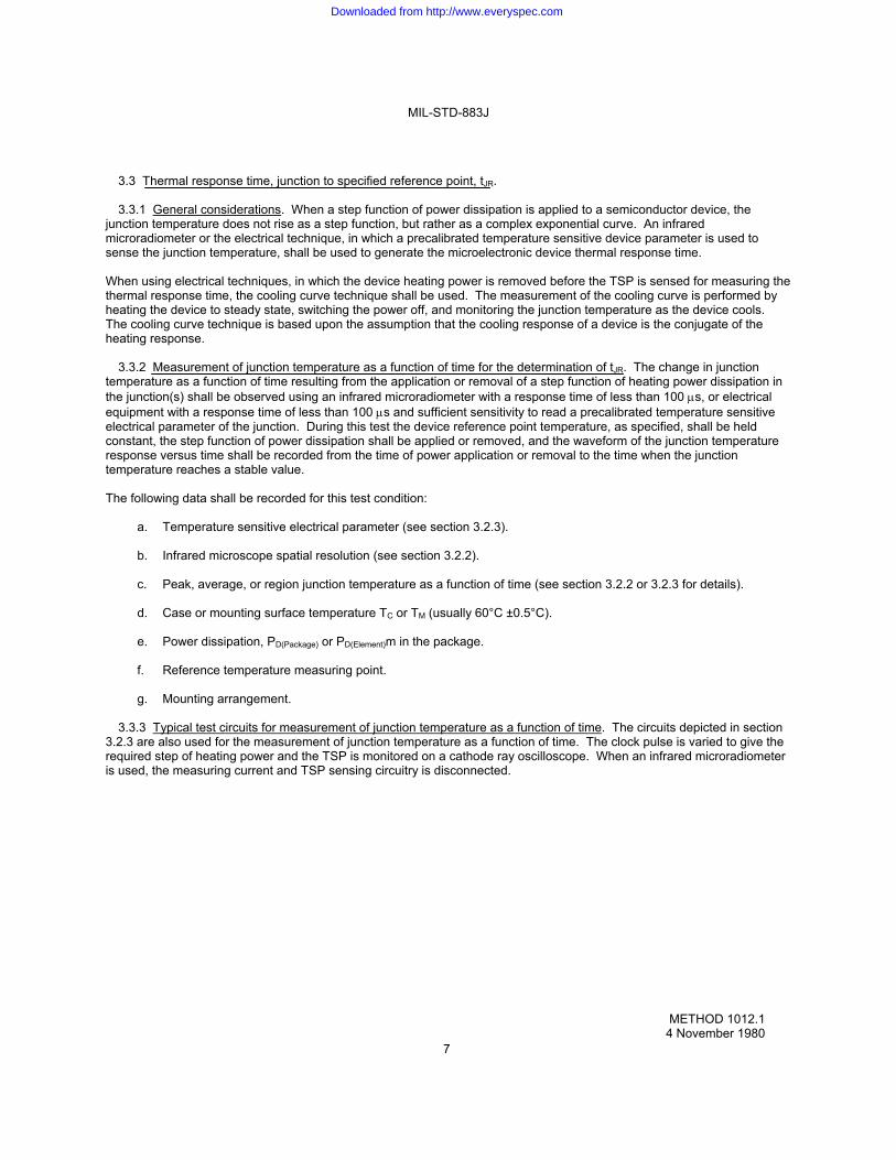
MIL-STD-883J
METHOD 1012.1 4 November 1980
7
3.3 Thermal response time, junction to specified reference point, tJR. 3.3.1 General considerations. When a step function of power dissipation is applied to a semiconductor device, the junction temperature does not rise as a step function, but rather as a complex exponential curve. An infrared microradiometer or the electrical technique, in which a precalibrated temperature sensitive device parameter is used to sense the junction temperature, shall be used to generate the microelectronic device thermal response time. When using electrical techniques, in which the device heating power is removed before the TSP is sensed for measuring the thermal response time, the cooling curve technique shall be used. The measurement of the cooling curve is performed by heating the device to steady state, switching the power off, and monitoring the junction temperature as the device cools. The cooling curve technique is based upon the assumption that the cooling response of a device is the conjugate of the heating response. 3.3.2 Measurement of junction temperature as a function of time for the determination of tJR. The change in junction temperature as a function of time resulting from the application or removal of a step function of heating power dissipation in the junction(s) shall be observed using an infrared microradiometer with a response time of less than 100 s, or electrical equipment with a response time of less than 100 s and sufficient sensitivity to read a precalibrated temperature sensitive electrical parameter of the junction. During this test the device reference point temperature, as specified, shall be held constant, the step function of power dissipation shall be applied or removed, and the waveform of the junction temperature response versus time shall be recorded from the time of power application or removal to the time when the junction temperature reaches a stable value. The following data shall be recorded for this test condition: a. Temperature sensitive electrical parameter (see section 3.2.3). b. Infrared microscope spatial resolution (see section 3.2.2). c. Peak, average, or region junction temperature as a function of time (see section 3.2.2 or 3.2.3 for details). d. Case or mounting surface temperature TC or TM (usually 60°C ±0.5°C). e. Power dissipation, PD(Package) or PD(Element)m in the package. f. Reference temperature measuring point. g. Mounting arrangement. 3.3.3 Typical test circuits for measurement of junction temperature as a function of time. The circuits depicted in section 3.2.3 are also used for the measurement of junction temperature as a function of time. The clock pulse is varied to give the required step of heating power and the TSP is monitored on a cathode ray oscilloscope. When an infrared microradiometer is used, the measuring current and TSP sensing circuitry is disconnected.
Downloaded from http://www.everyspec.com
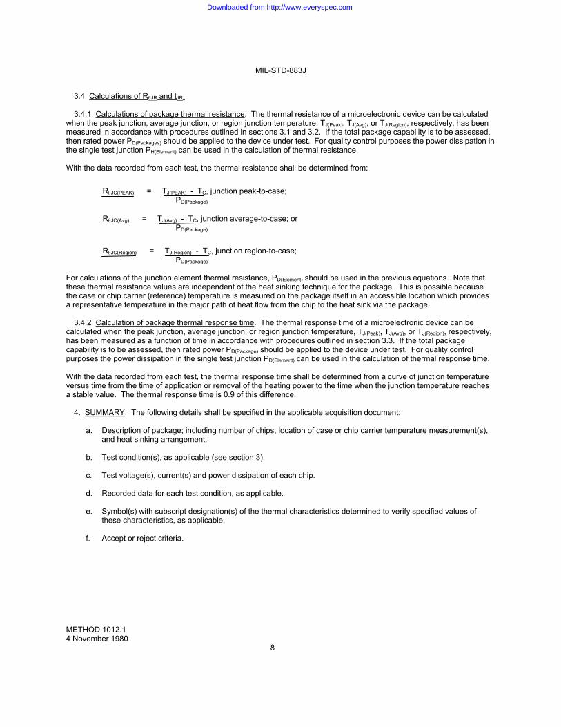
MIL-STD-883J
METHOD 1012.1 4 November 1980
8
3.4 Calculations of RJR and tJR. 3.4.1 Calculations of package thermal resistance. The thermal resistance of a microelectronic device can be calculated when the peak junction, average junction, or region junction temperature, TJ(Peak), TJ(Avg), or TJ(Region), respectively, has been measured in accordance with procedures outlined in sections 3.1 and 3.2. If the total package capability is to be assessed, then rated power PD(Packages) should be applied to the device under test. For quality control purposes the power dissipation in the single test junction PH(Element) can be used in the calculation of thermal resistance. With the data recorded from each test, the thermal resistance shall be determined from: RJC(PEAK) = TJ(PEAK) - TC, junction peak-to-case; PD(Package) RJC(Avg) = TJ(Avg) - TC, junction average-to-case; or PD(Package) RJC(Region) = TJ(Region) - TC, junction region-to-case; PD(Package) For calculations of the junction element thermal resistance, PD(Element) should be used in the previous equations. Note that these thermal resistance values are independent of the heat sinking technique for the package. This is possible because the case or chip carrier (reference) temperature is measured on the package itself in an accessible location which provides a representative temperature in the major path of heat flow from the chip to the heat sink via the package. 3.4.2 Calculation of package thermal response time. The thermal response time of a microelectronic device can be calculated when the peak junction, average junction, or region junction temperature, TJ(Peak), TJ(Avg), or TJ(Region), respectively, has been measured as a function of time in accordance with procedures outlined in section 3.3. If the total package capability is to be assessed, then rated power PD(Package) should be applied to the device under test. For quality control purposes the power dissipation in the single test junction PD(Element) can be used in the calculation of thermal response time. With the data recorded from each test, the thermal response time shall be determined from a curve of junction temperature versus time from the time of application or removal of the heating power to the time when the junction temperature reaches a stable value. The thermal response time is 0.9 of this difference. 4. SUMMARY. The following details shall be specified in the applicable acquisition document: a. Description of package; including number of chips, location of case or chip carrier temperature measurement(s),
and heat sinking arrangement. b. Test condition(s), as applicable (see section 3). c. Test voltage(s), current(s) and power dissipation of each chip. d. Recorded data for each test condition, as applicable. e. Symbol(s) with subscript designation(s) of the thermal characteristics determined to verify specified values of
these characteristics, as applicable. f. Accept or reject criteria.
Downloaded from http://www.everyspec.com
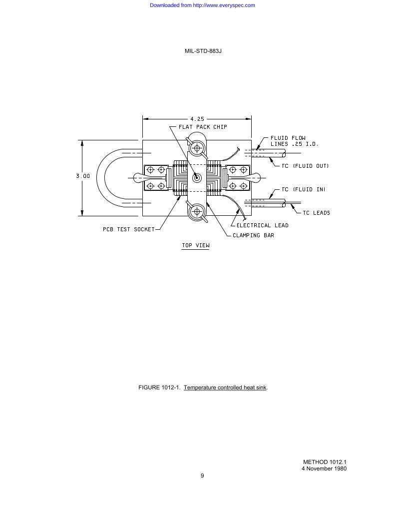
MIL-STD-883J
METHOD 1012.1 4 November 1980
9
FIGURE 1012-1. Temperature controlled heat sink.
Downloaded from http://www.everyspec.com
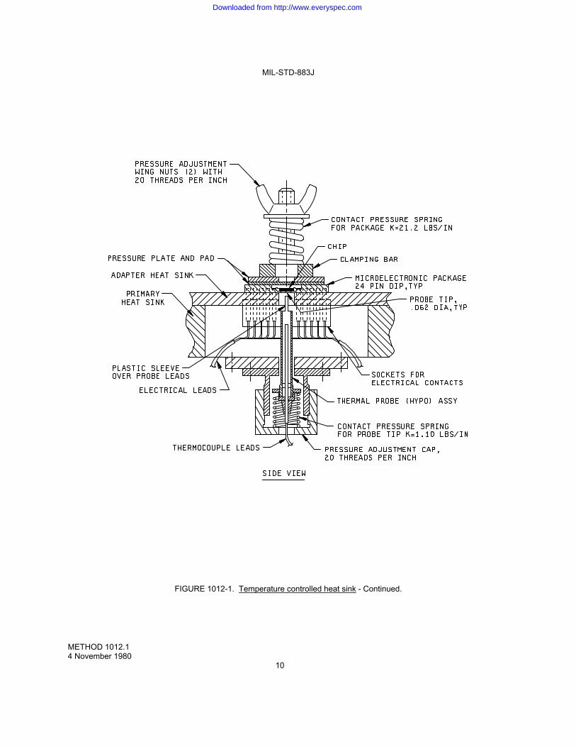
MIL-STD-883J
METHOD 1012.1 4 November 1980
10
FIGURE 1012-1. Temperature controlled heat sink - Continued.
Downloaded from http://www.everyspec.com
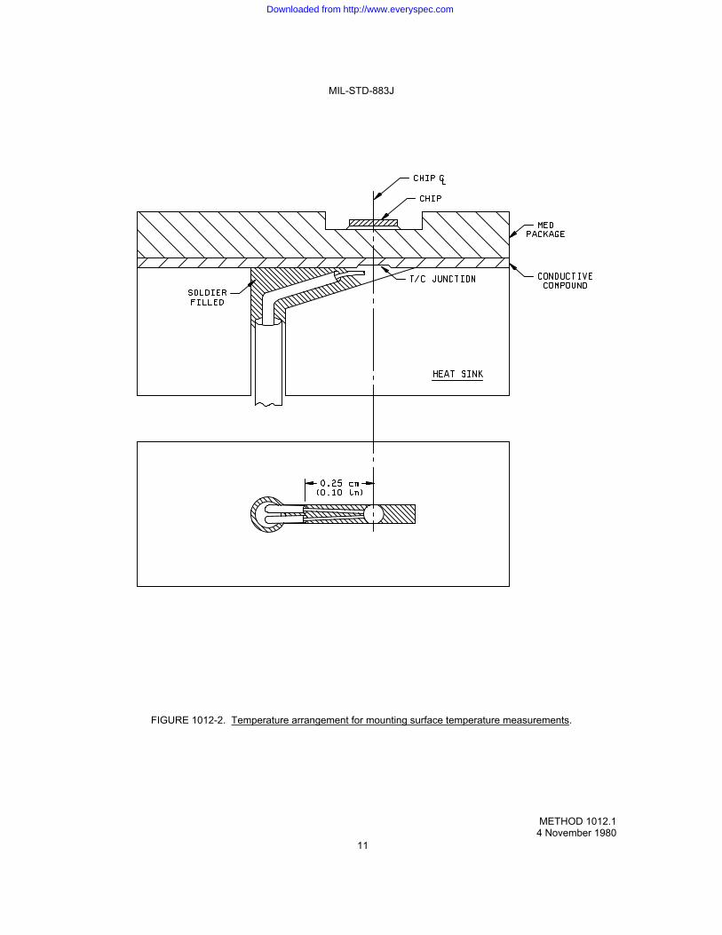
MIL-STD-883J
METHOD 1012.1 4 November 1980
11
FIGURE 1012-2. Temperature arrangement for mounting surface temperature measurements.
Downloaded from http://www.everyspec.com
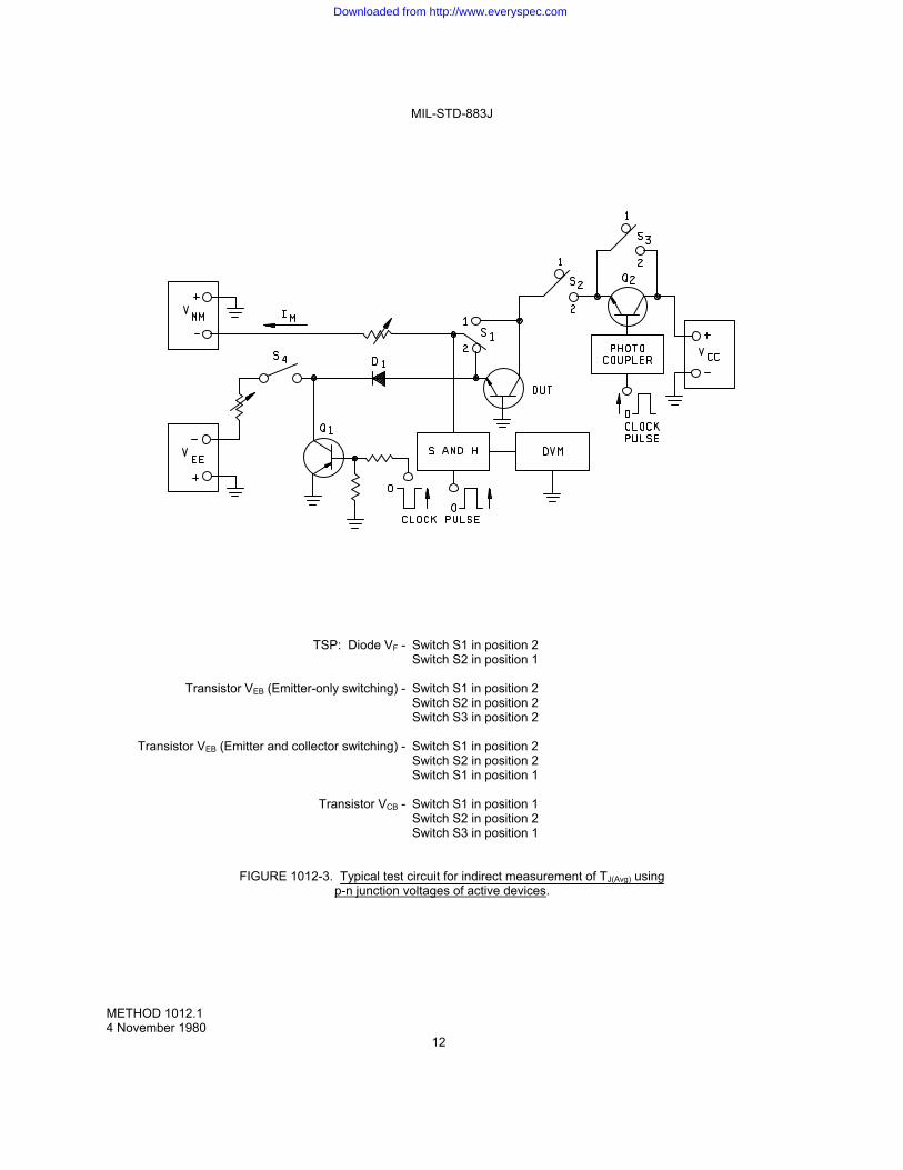
MIL-STD-883J
METHOD 1012.1 4 November 1980
12
TSP: Diode VF - Switch S1 in position 2 Switch S2 in position 1 Transistor VEB (Emitter-only switching) - Switch S1 in position 2 Switch S2 in position 2 Switch S3 in position 2 Transistor VEB (Emitter and collector switching) - Switch S1 in position 2 Switch S2 in position 2 Switch S1 in position 1 Transistor VCB - Switch S1 in position 1 Switch S2 in position 2 Switch S3 in position 1
FIGURE 1012-3. Typical test circuit for indirect measurement of TJ(Avg) using p-n junction voltages of active devices.
Downloaded from http://www.everyspec.com
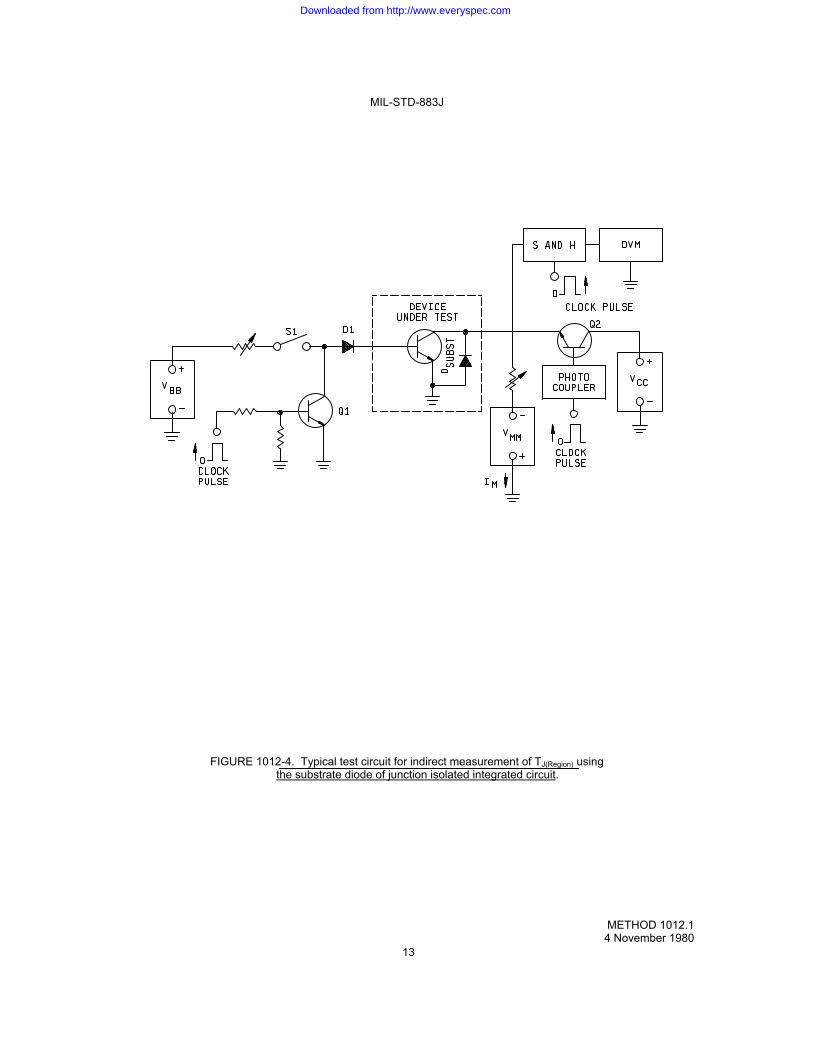
MIL-STD-883J
METHOD 1012.1 4 November 1980
13
FIGURE 1012-4. Typical test circuit for indirect measurement of TJ(Region) using the substrate diode of junction isolated integrated circuit.
Downloaded from http://www.everyspec.com
MIL-STD-883J
METHOD 1012.1 4 November 1980
14
This page intentionally left blank
Downloaded from http://www.everyspec.com
MIL-STD-883J
METHOD 1013 1 May 1968
1
METHOD 1013
DEW POINT 1. PURPOSE. The purpose of this test is to detect the presence of moisture trapped inside the microelectronic device package in sufficient quantity to adversely affect device parameters. The most sensitive indicator of moisture is device leakage current. This test specifies a lower temperature of -65°C for the normal dew point test. It may be desirable in some cases, where the presence of moisture in concentrations lower than that would be revealed at this lower temperature, to extend the lower temperature downward. 2. APPARATUS. The apparatus used in this test shall be capable of varying the temperature from the specified high temperature to -65°C while the parameter is being measured. 3. PROCEDURE. The voltage and current specified in the applicable acquisition document shall be applied to the terminals and the device leakage current or other specified parameter(s) continuously monitored from the specified high temperature to -65°C and back to the high temperature. The dew point temperature is indicated by a sharp discontinuity in the parameter being measured with respect to temperature. If no discontinuity is observed, it shall be assumed that the dew point is at a temperature lower than -65°C and the device being tested is acceptable. Devices which demonstrate instability of the measured parameter at any point during this test shall be rejected even though a true dew point is not identified. If a high temperature is not specified in the applicable acquisition document, the device shall be taken to a temperature at least 10°C above ambient temperature to initiate this test and enable detection of dew point in devices which may already be at saturation. The rate of change of temperature for this test shall be no greater than 10°C per minute. The test voltage shall be at least equal to the rated breakdown voltage of the device since it is necessary to apply sufficient voltage to achieve ionization. 4. SUMMARY. The following details shall be specified on the applicable acquisition document: a. Test temperature, high (see 3) and low if other than -65°C (see 1). b. Test voltage and current (see 3). c. Test parameter (see 1 and 3).
Downloaded from http://www.everyspec.com
MIL-STD-883J
METHOD 1013 1 May 1968
2
This page intentionally left blank
Downloaded from http://www.everyspec.com
MIL-STD-883J
METHOD 1014.14 7 June 2013
1
METHOD 1014.14
SEAL
1. PURPOSE. The purpose of this test is to determine the effectiveness (hermeticity) of the seal of microelectronic devices with designed internal cavities. 1.1 Definitions.
a. Standard leak rate. That quantity of dry air at 25C in atmosphere cubic centimeters flowing through a leak or multiple leak paths per second when the high-pressure side is at 1 atmosphere (760 mm Hg absolute) and the low-pressure side is at near total vacuum (see 1.1e below). Standard leak rate shall be expressed in units of atmosphere cubic centimeters per second of air (atm cm3/s air).
b. Measured leak rate. The implied leak rate that is measured on the detector for a given package using the specified
conditions and employing a specified test medium (tracer gas) specific to that detector. Measured leak rate is expressed in units of atmosphere cubic centimeters per second (atm cm3/s) for the medium used.
c. Leak-rate conversion factors for various test media.
atm cm3/s (Kr85) X 1.71 = atm cm3/s (air) atm cm3/s (Kr85) X 4.61 = atm cm3/s (He) atm cm3/s (He) X 0.37 = atm cm3/s (air) atm cm3/s (OLhe) X 0.37 = atm cm3/s (air)
d. Equivalent standard leak rate. The leak rate that a given package would have under the standard conditions of 1.1a. The
equivalent standard leak rate is determined by converting the implied leakage measured (La, R, Q or OLHe) to those conditions of 1.1c using appropriate calculations. For the purpose of comparison with rates determined by various media, the equivalent standard leak rate (for the medium used in the test) must be converted to the equivalent standard leak rate for the comparative medium (generally converted to air equivalents). The equivalent standard air leak rate shall be expressed in units of atmosphere cubic centimeters per second of air (atm cm3/s air). (1) La is the equivalent standard leak rate a package has expressed in term for air, or after converting to air from
another medium. (2) L is the maximum allowed equivalent standard leak rate La permitted for a package based on Table VII limits. For
pass/fail criteria, L is compared to La. (3) R is the implied leak rate of the medium (such as helium) as measured on a mass spectrometer. (4) R1 is the maximum allowed leak rate for the medium used. It is based on L using calculations to adjust for the
specific test conditions used in the measurement (see paragraph 2.1.2.3). For pass/fail criteria, R is compared to R1.
(5) Q is the implied leak rate of the medium (such as Krypton 85 (Kr85)) as measured on a radioisotope detector (see paragraph 2.2.6.c).
(6) Qs is the maximum allowed leak rate for the medium used. It is based on L using calculations to adjust for the specific test conditions used in the measurement (see paragraph 2.2.5.1). For pass/fail criteria, Q is compared to Qs
(7) OLHe is the implied leak rate (expressed in helium equivalents) as measured on an optical leak detector. e. Near total vacuum. The reduction of atmospheric pressure to 2 mm Hg or less, absolute.
f. Pounds per square inch absolute (psia) gas. The sum of gauge pressure in the tank and barometric pressure. A tank
showing zero gauge pressure is balancing the atmospheric conditions, hence has one atmosphere pressure (1 atm) inside. Absolute pressure takes this into consideration and is a measure of true content including this initial content. Thus, psia is the sum of the gauge pressure plus the barometric pressure.
*
Downloaded from http://www.everyspec.com
MIL-STD-883J
METHOD 1014.14 7 June 2013
2
1.2 Test Conditions. The following procedures are covered by this method:
1.2.1 Trace Gas (He). 1/
A1 Fixed Fine Leak A2 Flexible Fine Leak A4 Fine Leak, applicable to the unsealed package.
1.2.2 Radioisotope (Kr85).
B1 Fine Leak B2 Gross Leak B3 Wet Gross Leak
1.2.3 Perfluorocarbon Gross Leak.
C1 Fixed Method that uses a liquid bath. C2 has been replaced by C1. C3 Fixed Method that uses a vapor detection system instead of an indicator bath.
1.2.4 Optical.
C4 Gross Leak C5 Fine Leak
1.2.5 Penetrant Dye Gross Leak.
1.2.6 Weight Gain Gross Leak.
1.2.7 Radioisotope (Kr85).
G1 Thermal Leak Test for the evaluation of package hermetic integrity at elevated temperature.
1.2.8 Cumulative Helium Leak Detection (CHLD). CH1 Fixed Leak Detection for both Fine and Gross leak using the CHLD System. CH2 Flexible Leak Detection for both Fine and Gross leak using the CHLD System. Z He Gross Leak Detection combined with one of several other tracer gases for Fine Leak Detection using the CHLD
System. 1/ A3 was intentionally omitted.
Downloaded from http://www.everyspec.com
MIL-STD-883J
METHOD 1014.14 7 June 2013
3
1.3 Test Structure. Fine and gross leak tests shall be conducted in accordance with the requirements and procedures of the specified test condition. Testing order shall be fine leak (condition A or B1 or C5) followed by gross leak (condition B2, C1, C3, C4, D, or E) except when C4 or B2 is used together with A, B1, or C5. Condition B2 is a dry gas gross leak test and may be used prior to fine leak tests. When using the radioisotope tests, it is recommended practice to use B2 first to remove gross leakers prior to the fine leak test B1, which minimizes the Kr85 entrapped in rejected devices. When specified (see 4), measurements after test shall be conducted following the leak test procedures. Devices to be tested for thermal leakage shall first be subjected to a radioisotope gross leak test (B2), a radioisotope fine leak test (B1), or a gross/fine combination leak test, (B2/B1). Where bomb pressure specified exceeds the microcircuit package capability, alternate pressure, exposure time, and dwell time conditions may be used provided they satisfy the leak rate, pressure, time relationships which apply, and provided a minimum of 30 psia (2 atmospheres absolute) bomb pressure is applied in any case or for condition C4, a minimum of 10 psi differential test pressure is applied in any case. When test condition B2 is used to test large surface devices, a bomb pressure of 20 psia minimum may be used with the appropriate increase in bomb time (see paragraph 2.2.5.1). When test condition A4 is used, gross leak testing is not required. However A4 shall not be used in lieu of the required seal testing of lidded packages. When batch testing (more than one device in the leak detector at one time) is used in performing test condition A or B and a reject condition occurs it shall be noted as a batch failure. Each device may then be tested individually one time for acceptance if all devices in the batch are retested within one hour after removal from the tracer gas pressurization chamber. For condition B1, B2 only, devices may be batch tested and/or individually remeasured for acceptance providing all measuring is completed within one-half hour for B1 and within 10 minutes for B2 or combination B2/B1, after removal from the tracer gas pressurization chamber. For condition C3 only, devices that are batch tested, and indicate a reject condition, may be retested individually one time using the procedure of 2.3.4.1 herein, except that re-pressurization is not required if the devices are immersed in detector fluid within 20 seconds after completion of the first test, and they remain in the bath until retest. For conditions C4 and C5 only, the package must meet construction requirements defined in 2.4.1. This includes devices that are conformal coated such as circuit board assemblies.
1.3.1 Retest. Devices which fail gross leak may be retested destructively. If the retest shows a device to pass, that was originally thought to be a failure, then the device need not be counted as a failure in the accept number of sample size number calculations. Devices which fail fine leak shall not be retested for acceptance unless specifically permitted by the applicable acquisition document. The applicable acquisition document must also state that a failed device that passes retest needs not be counted as a failure in the sample size accept number calculations, otherwise if will count. Where fine leak retest is permitted, the entire leak test procedure for the specified test condition shall be repeated. That is, retest consisting of a second observation on leak detection without a re-exposure to the tracer fluid or gas under the specified test condition shall not be permissible under any circumstances. Preliminary measurement to detect residual tracer gas is advisable before any retest. 1.3.2 Failure criteria. The failure criteria for Fine Leak is provided in Table VII of paragraph 3. Failure criteria for other conditions; i.e., Gross Leak and Thermal Leak, is provided following the procedure for each individual test. 1.4 Apparatus. The apparatus required for the seal test shall be as indicated in the procedure for the applicable test condition being performed.
Downloaded from http://www.everyspec.com
MIL-STD-883J
METHOD 1014.14 7 June 2013
4
2. TEST CONDITIONS. 2.1 Test Conditions A1, A2, and A4 fine leak tracer gas (He). 1/
2.1.1 Apparatus. Apparatus required shall consist of suitable pressure and vacuum chambers and a mass spectrometer-type
leak detector preset and properly calibrated for a helium leak rate sensitivity sufficient to read measured helium leak rates of 10-9 atm cm3/s and greater. The volume of the chamber used for leak rate measurement should be held to the minimum practical, since this chamber volume has an adverse effect on sensitivity limits. The leak detector indicator shall be calibrated using a diffusion-type calibrated standard leak at least once during every working shift. In addition for test condition A4, the following apparatus is required: a. Fixture and fittings to mate the package to be tested to the leak detector. b. Surgical rubber gasket. c. Apiezon grease (type M or N), perfluorocarbon fluid 2/, or equivalent, if required to obtain seal. 2.1.2 Procedures. Test condition A1 is a "fixed" method with specified conditions in accordance with Table I that will ensure the test sensitivity necessary to detect the reject limit (R1). Test condition A2 is a "flexible" method that allows the variance of test conditions in accordance with the formula of 2.1.2.3 to detect the specified equivalent standard leak rate (L) at a predetermined reject limit (R1). Test condition A4 is a method that measures the leak rate (R) of an unsealed package. 2.1.2.1 Test conditions A1 and A2, procedures applicable to "fixed" and "flexible" methods. Insert the completed device(s) into the sealed chamber. The air inside the chamber shall then be evacuated to near total vacuum and then pressurized with 100 +0/-5 percent pure helium. Alternatively, a series of helium refills and vents may be performed until the minimum helium content is obtained. Once the required helium concentration is obtained the chamber can be set to the required pressure and time for the device(s). The pressure shall then be relieved and each specimen transferred to another chamber or chambers which are connected to the evacuating system and a mass-spectrometer-type leak detector. When the chamber(s) is evacuated, any tracer gas which was previously forced into the specimen will thus be drawn out and indicated by the leak detector as a measured leak rate (R). (The number of devices removed from pressurization for leak testing shall be limited such that the test of the last device can be completed within 60 minutes for test condition A1 or within the chosen value of dwell time t2 for test condition A2.) NOTE: The Flexible Method A2 shall be used unless otherwise specified in the acquisition document, purchase order, or contract. 1/ A3 was intentionally omitted. 2/ Perfluorocarbons contain no chlorine or hydrogen.
Downloaded from http://www.everyspec.com
MIL-STD-883J
METHOD 1014.14 7 June 2013
5
2.1.2.2 Test condition A1, fixed method. The devices(s) shall be tested using the appropriate conditions specified in Table I for the internal cavity volume of the package under test. The time t1 is the time under pressure and time t2 is the maximum time allowed after release of pressure before the device shall be read. The fixed method shall not be used if the maximum equivalent standard leak rate limit given in the acquisition document is less than the limits specified herein for the flexible method. 2.1.2.3 Test condition A2, flexible method. Values for bomb pressure exposure time, and dwell time shall be chosen such that actual measured tracer gas leak rate (R) readings obtained for the devices under test (if defective) will be greater than the minimum detection sensitivity capability of the mass spectrometer. The devices shall be subjected to a minimum of 2 atmospheres absolute of helium atmosphere. The chosen values, in conjunction with the value of the internal free volume of the device package to be tested and the maximum equivalent standard leak rate limit (L) (as shown below or as specified in the applicable acquisition document), shall be used to calculate the reject limit (R1) using the following formula (see Eq (1)):
2
1
2
1
12
1 0
2
0
1
1
M
M
VP
Lt
e
M
M
VP
Lt
eM
M
P
LPR
AA
A
O
E
Where: R = The actual leakage measurement of tracer gas (He) through the leak in atm cm3/s He. R1 = The calculated reject limit maximum allowable leakage measurement. L = The maximum allowable equivalent standard leak rate limit (see Table VII of paragraph 3) in atm cm3/s air. PE = The pressure of exposure in atmospheres absolute. PO = The atmospheric pressure in atmospheres absolute. (1 atm) MA = The molecular weight of air in grams (28.96). M = The molecular weight of the tracer gas (He) in grams. (4 amu’s) t1 = The time of exposure to PE in seconds. t2 = The dwell time between release of pressure and leak detection, in seconds. V = The internal free volume of the device package cavity in cubic centimeters. 2.1.3 Failure criteria. The failure criteria for Fine Leak is provided in Table VII of paragraph 3. 2.1.4 Test condition A4, procedure applicable to the unsealed package method. The fixture and fittings of 2.1.1.a. shall be mounted to the evacuation port of the leak detector. Proof of fixturing integrity shall be verified by sealing a flat surfaced metal plate utilizing the gasket of 2.1.1b (and grease or fluid of 2.1.1.c if required to obtain seal) and measuring the response of the leak test system. Testing shall be performed by sealing the package(s) to the evacuation port and the package cavity evacuated to 0.1 torr or less. Care shall be taken to prevent contact of grease with package (seal ring not included) to avoid masking leaks. The external portion of the package shall be flooded with Helium gas either by the use of an envelope or a spray gun, at a pressure of 10 psig. 2.1.4.1 Failure criteria. Unless otherwise specified, devices shall be rejected if the measured leak rate (R) exceeds 1 X 10⁻⁸ atm cm3/s He.
Eq (1)
Downloaded from http://www.everyspec.com
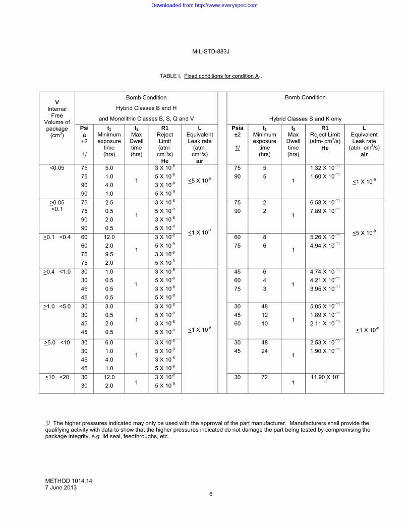
MIL-STD-883J
METHOD 1014.14 7 June 2013
6
TABLE I. Fixed conditions for condition A1.
1/ The higher pressures indicated may only be used with the approval of the part manufacturer. Manufacturers shall provide the qualifying activity with data to show that the higher pressures indicated do not damage the part being tested by compromising the package integrity, e.g. lid seal, feedthroughs, etc.
V
Internal Free
Volume of package
(cm3)
Bomb Condition
Hybrid Classes B and H
and Monolithic Classes B, S, Q and V
Bomb Condition
Hybrid Classes S and K only
Psia ±2
1/
t1 Minimum exposure
time (hrs)
t2 Max
Dwell time (hrs)
R1 Reject Limit (atm-cm3/s)
He
L Equivalent Leak rate
(atm-cm3/s)
air
Psia ±2
1/
t1 Minimum exposure
time (hrs)
t2 Max
Dwell time (hrs)
R1 Reject Limit (atm- cm3/s)
He
L Equivalent Leak rate
(atm- cm3/s) air
<0.05 75
75
90
90
5.0
1.0
4.0
1.0
1
3 X 10⁻⁸
5 X 10⁻⁹
3 X 10⁻⁸
5 X 10⁻⁹
<5 X 10⁻⁸
75
90
5
5 1
1.32 X 10⁻¹¹
1.60 X 10⁻¹¹ <1 X 10⁻⁹
>0.05 <0.1
75
75
90
90
2.5
0.5
2.0
0.5
1
3 X 10⁻⁸
5 X 10⁻⁹
3 X 10⁻⁸
5 X 10⁻⁹ <1 X 10⁻⁷
75
90
2
2 1
6.58 X 10⁻¹¹
7.89 X 10⁻¹¹
<5 X 10⁻⁹ >0.1 <0.4 60
60
75
75
12.0
2.0
9.5
2.0
1
3 X 10⁻⁸
5 X 10⁻⁹
3 X 10⁻⁸
5 X 10⁻⁹
60
75
8
6 1
5.26 X 10⁻¹¹
4.94 X 10⁻¹¹
>0.4 <1.0 30
30
45
45
1.0
0.5
0.5
0.5
1
3 X 10⁻⁸
5 X 10⁻⁹
3 X 10⁻⁸
5 X 10⁻⁹
<1 X 10⁻⁶
45
60
75
6
4
3 1
4.74 X 10⁻¹¹
4.21 X 10⁻¹¹
3.95 X 10⁻¹¹
<1 X 10⁻⁸
>1.0 <5.0 30
30
45
45
3.0
0.5
2.0
0.5
1
3 X 10⁻⁸
5 X 10⁻⁹
3 X 10⁻⁸
5 X 10⁻⁹
30
45
60
48
12
10 1
5.05 X 10⁻¹¹
1.89 X 10⁻¹¹
2.11 X 10⁻¹¹
>5.0 <10 30
30
45
45
6.0
1.0
4.0
1.0
1
3 X 10⁻⁸
5 X 10⁻⁹
3 X 10⁻⁸
5 X 10⁻⁹
30
45
48
24 1
2.53 X 10⁻¹¹
1.90 X 10⁻¹¹
>10 <20 30
30
12.0
2.0 1 3 X 10⁻⁸
5 X 10⁻⁹
30 72 1
11.90 X 10-
11
Downloaded from http://www.everyspec.com
MIL-STD-883J
METHOD 1014.14 7 June 2013
7
2.2 Test Condition B, Radioisotope.
2.2.1 Radioisotope leak test apparatus. Apparatus for this test shall consist of:
a. Radioactive tracer gas pressurization console containing a Kr85/air mixture.
b. Counting equipment consisting of a scintillation crystal, photomultiplier tube, preamplifier, ratemeter, and Kr85 reference
standards. The counting station shall be of sufficient sensitivity to determine through the device wall the radiation level of any Kr85 tracer gas present within the device.
(1) A “Flat Top Scintillation Crystal” counting station shall have a minimum sensitivity of 4,500 c/m/µCi Kr85 and a
minimum detectable count rate of 500 counts per minute above ambient background.
(2) A “Well Crystal” counting station shall have a minimum sensitivity of 10,000 c/m/µCi Kr85 and a minimum detectable count rate of 500 counts per minute above ambient background.
(3) A “Tunnel Crystal” counting station shall have a minimum sensitivity of 4,500 c/m/µCi Kr85 and a minimum detectable count rate of 500 counts per minute above ambient background.
The counting station shall be calibrated at least once every working shift using Kr85 reference standards and following the equipment manufacturer's instruction. The actual calibration reading shall be recorded for each scintillation crystal detection system (Well, Tunnel, and Flat top) prior to performing testing.
c. A tracer gas that consists of a mixture of Kr85 and air. The concentration of the Kr85 in the Kr85/air mixture shall be no less than 100 micro-curies per atmospheric cubic centimeter. The determined values of each analytical sample shall be recorded in accordance with the calibration requirements of this standard (see 4.5.1 of MIL-STD-883). The specific activity may be measured automatically by the equipment during cycling of the equipment. If not, then an analytical sample of the Kr85 shall be taken at least once each 30 days to determine when the concentration drops by 5 percent in concentration and specific activity. If production use of the pressurization console averages 1000 of fewer bombings during the month analytical sampling may be annually. When the concentration drops by 5 percent, corrective action shall be taken to adjust the concentration.
d. ESD Protective Tubes shall be utilized to ensure the system is ESD safe when using the Well Counting Station. e. All calibration records (e.g. daily, monthly, voltage crystal plateau graphs, and C of C for Kr85 reference standard, specific
activity etc.) shall be maintained and made available to the qualifying activity. f. The crystal voltage plateau graph shall be performed and documented semiannually. Examples of good plateau graphs
and bad plateau graphs shall be included in the internal procedure.
2.2.2 Test condition B2 – radioisotope gross leak package qualification. This test shall be used to qualify all packages with less than 0.1 cm3 internal free volume that will undergo screening tests per the B2 radioisotope gross leak, or the B2/B1 gross/fine leak combination test (see paragraph 2.2.6.b and c). The purpose is to assure that if such a packages has a leak, then that leak will be detectable under test conditions B2 and B2/B1. Packages having 0.1 cm3 internal free volume or larger do not require package qualification. Packages smaller than 0.1 cm3 internal free volume shall be subjected to the following requirements:
a. A 5 mil diameter hole shall be made in a representative sample of the devices to be tested.
b. The device shall be subjected to this test condition and removed from the pressurization tank. The device shall be measured in the counting station immediately after the tank is vented to atmosphere. A “net” reading indication of 500 counts per minute or greater is considered a reject. The device must remain a reject with a minimum of 500 counts per minute above ambient background for ten minutes after removal from the pressurization tank. If the device does not fail, test conditions B2 and B2/B1 shall not be used.
Downloaded from http://www.everyspec.com
MIL-STD-883J
METHOD 1014.14 7 June 2013
8
2.2.3 Test condition B2 and B1 - radioisotope gross/fine combination leak. The apparatus for this test is that of paragraph 2.2. This test may be applied as a combination of conditions B2/B1 and is used in accordance with the requirements of those conditions for specified packages, as qualified under paragraph 2.2.2, with an atmosphere of Kr85/air mixture. Actual pressure and soak time for B1 shall be determined in accordance with paragraph 2.2.5.1. When the soak time is completed, the Kr85/air mixture shall be evacuated until 2.0 torr pressure exists in the pressurization chamber. The evacuation shall be completed within 3 minutes from either the end of the pressurization cycle or the point at which the chamber pressure reaches 60 psia (if a higher pressure than 60 psia was used). The chamber shall then immediately be backfilled with air and the test devices removed from the chamber. The devices shall be measured using a scintillation crystal equipped counting station as specified in paragraphs 2.2.4.1, 2.2.4.2, or 2.2.5.2. Devices subjected to this gross/fine combination test must be measured within 10 minutes after removal from the pressurization system. The R value shall not be less than 500 counts per minute above background. If all of the tested devices cannot be measured within 10 minutes after removal from the pressurization cycle, the remaining devices at 10 minutes must be re-tested as above in this paragraph.
2.2.4 Determination of counting efficiency (k). The counting efficiency (k), or k-factor, is the efficiency of measurement of
radioactive Kr85 tracer gas within a device using a scintillation crystal as a detector. The k-factor must be determined for the combination of both the scintillation crystal detection system that is to be used for the measurement and for the specific geometry of the device to be tested (see 2.2.4.1, 2.2.4.2, 2.2.4.3, or 2.2.5.2). This is done using a device ‘sample’ of the same geometric configuration as the device to be tested. The geometric center of the cavity, or its internal void, is the point called the “center of mass” of the radioactive gas being measured. The location of the center of mass is the point referred to for the k-factor of the device as it is positioned in each of the scintillation crystal detection systems described in 2.2.4.1, 2.2.4.2, 2.2.4.3, or 2.2.5.2. Once established, the k-factor for each package configuration shall be recorded. This record shall list the methodology and procedure used to obtain the k-factor and shall be made available to the qualifying activity upon request.
2.2.4.1 Scintillation “Well-Crystal”.
a. A representative sample, consisting of a device with the same geometric configuration as the test sample device(s), shall be used to determine the counting efficiency (k). This representative sample shall have an accurately known micro-curie content of Kr85 placed within its internal void.
b. The counts per minute from the representative sample shall be measured in the well of the shielded scintillation crystal of
the counting station. The sample device should be in the exact position as test devices will be tested. If not, then the sample device shall be located at a height not to be exceeded by any device tested (see note below). From this measured value the counting efficiency, in counts per micro-curie, shall be calculated for that device/crystal system.
Note: The counting efficiency of the scintillation well crystal is reduced systematically at higher locations within the
crystal’s well. The k-factor for the sample at the bottom of the well will be the greatest. If a device is placed on top of other devices such as in testing multiple devices simultaneously, then the top device will have the least measured k-factor effect. Thus, the measured k-factor, determination using the sample device located other than at the bottom of the crystal’s well, determines the maximum height to be allowed for the actual test. This height shall be established and shall not be exceeded by any actual test device, including any one of the multiple devices being simultaneously tested.
2.2.4.2 Scintillation “Flat-Top Crystal”.
a. A representative sample consisting of a device with the same geometric configuration as the test sample device(s) shall be
used to determine the counting efficiency (k). This representative sample shall have an accurately known micro-curie content of Kr85 placed within its internal void.
b. The counts per minute from the representative sample shall be measured on the shielded scintillation crystal of the
counting station. The sample must be in the exact position as the actual test devices will be tested. The k-factor for the sample shall be measured with the sample placed flat in a position centered to the main body of the crystal. Some flat-top crystals are solid cylinders of approximately 3 inches diameter, and the device sample is placed on the cylinder in the same manner, as mentioned. From this measured value, the counting efficiency, in counts per minute per micro-curie shall be calculated for that device/crystal system.
Downloaded from http://www.everyspec.com
MIL-STD-883J
METHOD 1014.14 7 June 2013
9
2.2.4.3 Scintillation “Tunnel Crystal”.
a. A Tunnel Crystal is either a solid block scintillation crystal similar to a flat-top crystal with an open tunnel through the body
or can be a pair of solid scintillation crystals place one above the other in a parallel configuration. Devices pass through the tunnel or between the parallel crystals, usually on a conveyer belt, allowing dynamic measurements. This configuration is commonly used in high volume testing.
b. The k-factor must be determined for the Tunnel Crystal’s dynamic condition which is usually less than in a static condition with
the device standing at the center of the tunnel. See paragraph 2.2.5.2 to establish the k-factor for the sample using such a configuration. Alternately, this k-factor determination is commonly determined by the manufacturer upon request.
2.2.5 Test condition B1, radioisotope fine or B2/B1 gross/fine leak combination test.
2.2.5.1 Testing parameters. The bombing pressure and soak time shall be determined in accordance with the following formula (see Eq (2)):
skTPt
RQS
Where: QS = The calculated maximum leak rate allowable, in atm cm3/s Kr, for the devices to be tested. R = Counts per minute above the ambient background after pressurization if the device leak rate were exactly equal to
QS. This is the reject count above the background of both the counting equipment and the background reading of the microcircuit, if it has been through prior radioactive leak tests.
s = The specific activity, in micro-curies per atmosphere cubic centimeter of the Kr85 tracer gas in the pressurization
system. k = The counting efficiency of the specific scintillation crystal used in the testing to measure Kr85 within the internal
cavity of the specific component being evaluated. This k-factor must be determined in accordance with 2.2.4 for each device geometric configuration in combination with the specific scintillation crystal in which it will be measured.
T = Soak time, in hours, that the devices are to be pressurized. P = Pe
2-Pi 2, where Pe is the bombing pressure in atmospheres absolute and Pi is the original internal pressure of the
devices in atmospheres absolute. The activation pressure (Pe) may be established by specification or if a convenient soak time (T) has been established, the activation pressure (Pe) can be adjusted to satisfy equation (1).
t = Conversion of hours to seconds and is equal to 3,600 seconds per hour. NOTE: The complete version of equation (1) contains a factor (PO 2 - ( P)2) in the numerator which is a correction factor for
elevation above sea level. PO is sea level pressure in atmospheres absolute and P is the difference in pressure, in atmospheres between the actual pressure at the test station and sea level pressure. For the purpose of this test method, this factor has been dropped.
Eq (2)
Downloaded from http://www.everyspec.com
MIL-STD-883J
METHOD 1014.14 7 June 2013
10
2.2.5.2 Dynamic Measurement of the k-factor with a Scintillation-Crystal.
a. A representative sample consisting of a device with the same geometric configuration as the test sample device(s) shall be
used to determine the counting efficiency (k). This representative sample shall have an accurately known micro-curie content of Kr85 placed within its internal void.
b. A crystal, (or crystals), can be used for dynamic testing of devices passing over or through the crystal(s). This configuration
is commonly used in high volume testing. The k-factor must be determined in the ‘dynamic condition’, which will establish a k-factor value, (usually less than in a static condition with the device standing at the center of the tunnel.) The representative sample is measured dynamically, as it passes through the crystal. This establishes the maximum reading achievable for the sample. From this measured value, the counting efficiency, in counts per minute per micro-curie shall be calculated. This k-factor determination is most commonly determined by the equipment manufacturer.
2.2.5.3 Geometric configurations. The k-factor for each geometric configuration is determined and used for testing. As a
convenience, the same k-factor may apply to similar geometric configurations. This allows the same k-factor to be used for multiple devices, as long as the same test procedure and equipment is used, and the devices are measured using the same measurement system, (2.2.4.1, 2.2.4.2, or 2.2.5.2).
Scintillation “well” crystals are capable of detecting (measuring) a maximum reading of 16,000 to 18,000 counts per minute from the emission of one micro-curie of Kr85 contained within the cavity of a device. This maximum reading of Kr85 emission is achieved with the DUT placed deep into the well-crystal and with no shielding from other devices or fixtures.
The counting efficiency (k-factor) for most device configurations and crystal combinations may be available from the equipment manufacturer by providing the equipment manufacturer with representative samples of the same geometric configuration as the device to be tested. Suitable facilities shall retain record of how the k-factor was established for each package configuration and made available to the qualifying activity.
2.2.5.4 Evaluation of surface sorption and wait time. All device encapsulations consisting of glass, metal, and ceramic or combinations thereof, that also include external coatings and external sealants or labels, shall be evaluated for surface sorption of Kr85 before establishing the leak test parameters. Devices susceptible to surface sorption must “wait” for the surface sorption to dissipate before being tested. This time lapse shall be noted and shall determine the "wait time" specified in 2.2.6.
Representative samples with the questionable surface material shall be subjected to the predetermined pressure and time conditions established for the device configuration as specified by 2.2.5.1. The samples shall then be measured at the counting station every 10 minutes, with count rates noted. The total time taken for the count rate to become asymptotic is the “wait time”.
Devices which are determined to have surface absorption should first be subjected to the radioisotope gross leak test procedure (B2), and then to the fine leak test (B1). The gross leak procedure will remove all leaking devices with leak rates greater than 5 X 10⁻⁶ atm-cm3/sec.
2.2.5.4.1 Alternate β method. The surface sorption can also be determined by measuring the Beta (β) emission from any Kr85 absorbed into surface materials. The β particles will not penetrate the walls of the device; therefore, β emission detection means Kr85 is on the outer surfaces of a device. The β readings are monitored until they dissipate confirming the surface is free of Kr85 gas. This time to dissipate is the “wait time”.
2.2.5.4.2 Removal of surface sorption. Devices with cavities > 0.1 cm3, with leak rates in the fine leak range, will not lose their internal Kr85 gas in < 1 Hour. Therefore, such devices may be placed in a vacuum-oven at temperatures up to 100ºC and near total vacuum for 15-20 minutes following pressurization for B1 without the concern of losing internal Kr85. This vacuum-oven procedure is capable of removing surface absorbed Kr85 from paints and labels. The removal of that surface Kr85 from the surface materials is accurately confirmed by verifying that there is no Beta radiation from the surface.
Downloaded from http://www.everyspec.com
MIL-STD-883J
METHOD 1014.14 7 June 2013
11
2.2.6 Test Procedure B1, Fine Leak; B2, Gross Leak; or B2/B1 Gross/Fine combination test. The devices shall be placed in a
radioactive tracer gas pressurization chamber. The pressurization chamber may be partially filled with inert material (aluminum filler blocks), to reduce the cycle time and increase the efficiency of the system. It is the equipment manufacturer’s recommendation that all ‘small-cavity’ devices be measured within 10 minutes after removal from the pressurization tank.
a. B1 - Fine Leak: The tank shall be evacuated to 0.5 torr. The devices shall be subjected to a minimum of 2 atmospheres absolute pressure of Kr85/air mixture. Actual pressure and soak time for B1 shall be determined in accordance with 2.2.5.1. When the ‘soak time’ is completed, the Kr85/air mixture shall be transferred to storage until 0.5 torr pressure exists in the pressurization chamber. The storage cycle shall be completed in 3 minutes maximum as measured from the end of the pressurization cycle or from the time the tank pressure reaches 60 psia if a higher bombing pressure was used. The tank shall then immediately be backfilled with air and the devices removed from the tank and measured within 1 hour after removal using a scintillation crystal equipped counting station as in 2.2.4.1, 2.2.4.2, or 2.2.5.2. Device encapsulations that come under the requirements of 2.2.5.4 shall be exposed to ambient air for a time not less than the ‘wait time’ determined by 2.2.5.4 (or following the bake cycle described in 2.2.5.4.2). Device encapsulations that do not come under the requirements of 2.2.5.4 may be tested without a ‘wait time’. The R value of 2.2.5.1 shall not be less than 500 counts per minute above background.
Note: If the devices are tested in the well crystal with the crystal wall shielded with a lead plug while measuring the device, and a background of approximately 500 counts per minute is achievable when the Ratemeter is in the “slow-time-constant” position, then reject values “R” of a minimum of 250 counts (net) above background may be measured for rejection of devices in high sensitivity testing.
b. B2 - Gross Leak: Only product qualified under paragraph 2.2.2 shall be authorized to use this method. The devices shall
be placed in a pressure chamber. The chamber shall be filled with inert material (aluminum filler blocks) so that the free volume is not greater than as qualified in 2.2.2. The tank shall be evacuated to 0.5 torr. The devices shall be subjected to a minimum of 2 atmospheres absolute pressure of Kr85/air mixture and the bomb time no less than 2 minutes. When the soak time is completed the Kr85/air mixture shall be transferred to storage until 2.0 torr pressure exists in the pressurization tank. The storage cycle shall be completed in 3 minutes maximum as measured from the end of the pressurization cycle. The tank shall then immediately be backfilled with air. The devices shall be removed from the tank and measured within 10 minutes after removal using a scintillation crystal equipped counting station as in 2.2.4.1, 2.2.4.2, 2.2.4.3 or 2.2.5.2. Any device indicating 500 counts per minute, or greater, above the ambient background of the counting station shall be considered a gross leak failure. If the devices are not all measured at the end of 10 minutes from removal from the pressurization chamber, the remaining devices shall be returned to the pressurization chamber and re-pressurized to a minimum of 30 psia for a minimum of 0.01 hrs, and then measured at the counting station within 10 minutes. The counting station shall be checked at least once every shift using a Kr85 reference standard following manufacturer’s procedure, and a record of proper function shall be maintained.
Downloaded from http://www.everyspec.com
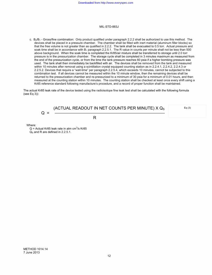
MIL-STD-883J
METHOD 1014.14 7 June 2013
12
c. B2/B1 - Gross/fine combination: Only product qualified under paragraph 2.2.2 shall be authorized to use this method. The
devices shall be placed in a pressure chamber. The chamber shall be filled with inert material (aluminum filler blocks) so that the free volume is not greater than as qualified in 2.2.2. The tank shall be evacuated to 0.5 torr. Actual pressure and soak time shall be in accordance with B1 paragraph 2.2.5.1. The R value in counts per minute shall not be less than 500 above background. When the soak time is completed the Kr85/air mixture shall be transferred to storage until 2.0 torr pressure is in the pressurization chamber. The storage cycle shall be completed in 3 minutes maximum as measured from the end of the pressurization cycle, or from the time the tank pressure reaches 60 psia if a higher bombing pressure was used. The tank shall then immediately be backfilled with air. The devices shall be removed from the tank and measured within 10 minutes after removal using a scintillation crystal equipped counting station as in 2.2.4.1, 2.2.4.2, 2.2.4.3 or 2.2.5.2. Devices that require a “wait-time” per paragraph 2.2.5.4, which exceeds 10 minutes, cannot be subjected to this combination test. If all devices cannot be measured within the 10 minute window, then the remaining devices shall be returned to the pressurization chamber and re-pressurized to a minimum of 30 psia for a minimum of 0.01 hours, and then measured at the counting station within 10 minutes. The counting station shall be checked at least once every shift using a Kr85 reference standard following manufacture’s procedure, and a record of proper function shall be maintained.
The actual Kr85 leak rate of the device tested using the radioisotope fine leak test shall be calculated with the following formula (see Eq 3)):
(ACTUAL READOUT IN NET COUNTS PER MINUTE) X QS Q = R
Where: Q = Actual Kr85 leak rate in atm cm3/s Kr85 QS and R are defined in 2.2.5.1.
Eq (3)
Downloaded from http://www.everyspec.com
MIL-STD-883J
METHOD 1014.14 7 June 2013
13
2.2.7 Test condition B3, Radioisotope Wet Gross Leak Test.
2.2.7.1 Intended Use. This is designed for small packages with less than 0.1 cm3 internal free volume and packages that have
not qualified to 2.2.2. This test may be used for larger than 0.1 cm3 internal free volume packages. Packages up to 0.1 cm3 internal free volume suspected of very large leaks are commonly subjected to this test.
2.2.7.2 Apparatus. Apparatus for this test shall be as in 2.2.1 and as follows:
a. A container of sufficient volume to allow the devices to be covered with red dye penetrant solution, evacuated, and subjected to air pressure in the same container.
b. Solutions:
(1) The red dye penetrant solution shall be kept clean and free of contaminants (including wash solvents). The
solutions shall be tested to verify the efficiency of the solution for both Kr85 gettering and visual detectability. The most efficient red dye solution uses a mixture, by volume, of 95% light viscosity mineral oil and 5% oil-based red dye indicator. The solution must be evaluated for Kr85 absorption and retention.
(2) The solvent for washing the devices after immersion shall be acetone.
2.2.7.3 Procedure. The following four steps shall be followed:
Step 1. The devices shall be immersed in the red dye penetrant solution and evacuated to a pressure of 100 torr (~ 24 inches Hg) or less for 10 minutes and then pressurized with air for 10 minutes minimum at 310 kPa (45 psia) minimum. The devices shall be removed from the red dye penetrant solution and placed in a fine-screen basket and flushed with acetone by applying a fine-spray of acetone to remove the surface film of the solution. It is recommended that the devices in the fine-screen basket be held over funnel, with the funnel inserted into a large Erlenmeyer flask, (thus minimizing the acetone vapors released into the room). Do not allow any acetone to contaminate the red dye penetrant solution. Immediately following the wash, the devices shall be emptied onto a white surface and examined visually for red dye penetrant solution exiting from any leaking devices. Look for evidence of red dye leakage that is apparent without using the aid of visual magnification. Any devices with red dye penetrant solution leaking from them shall be rejected as gross leakers and removed. Step 2. The remaining devices shall then be placed in the radioisotope pressurization chamber. The chamber shall be filled with inert material (aluminum filler blocks) so that the free volume is not greater than as qualified in 2.2.2. The chamber is evacuated to a pressure of 0.5 torr. The devices shall then be pressurized to a minimum of 45 psia of Kr85/air mixture for 0.2 hours minimum. The gas shall then be transferred to storage until a pressure of 2.0 torr maximum exists in the tank. This transfer shall be completed in 2 minutes maximum. The chamber shall then be filled with air, and the devices immediately removed from the tank and leak tested within 5 minutes after gas exposure, with a scintillation crystal equipped counting station. It is recommended that batch sizes be kept small enough to allow all devices to be measured within 5 minutes. Any device indicating 500 c/m or greater above the ambient background of the counting station shall be considered a gross leak. If all of the devices cannot be measured within 5 minutes, they shall be retested starting at the beginning of step 2. Step 3. Failing devices may cross contaminate compliant devices with red dye penetrant solution. Devices which contain red dye penetrant solution may effervesce after being pressurized with Kr85 and may lose the Kr85 trapped within them. The devices shall be emptied onto a white surface and examined carefully for any red dye penetrant solution exiting from any leaking devices. Any devices with red dye penetrant solution leaking from them shall be rejected as gross leakers. Gross leak failures with less than 0.1 cm3 internal free volume shall be visually inspected at 30X to confirm that the red dye penetrant solution is actually leaking from the device. Step 4. If any devices are rejected by Steps 1 – 3, the procedure (starting with Step 2) shall be performed again until no more gross leakers are found.
Downloaded from http://www.everyspec.com
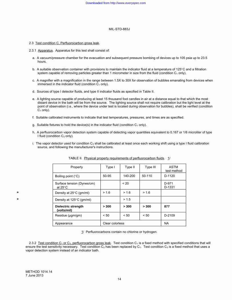
MIL-STD-883J
METHOD 1014.14 7 June 2013
14
2.3 Test condition C, Perfluorocarbon gross leak.
2.3.1 Apparatus. Apparatus for this test shall consist of:
a. A vacuum/pressure chamber for the evacuation and subsequent pressure bombing of devices up to 105 psia up to 23.5
hours. b. A suitable observation container with provisions to maintain the indicator fluid at a temperature of 125C and a filtration
system capable of removing particles greater than 1 micrometer in size from the fluid (condition C1 only). c. A magnifier with a magnification in the range between 1.5X to 30X for observation of bubbles emanating from devices when
immersed in the indicator fluid (condition C1 only). d. Sources of type I detector fluids, and type II indicator fluids as specified in Table II. e. A lighting source capable of producing at least 15 thousand foot candles in air at a distance equal to that which the most
distant device in the bath will be from the source. The lighting source shall not require calibration but the light level at the point of observation (i.e., where the device under test is located during observation for bubbles), shall be verified (condition C1 only).
f. Suitable calibrated instruments to indicate that test temperatures, pressures, and times are as specified. g. Suitable fixtures to hold the device(s) in the indicator fluid (condition C1 only). h. A perfluorocarbon vapor detection system capable of detecting vapor quantities equivalent to 0.167 or 1/6 microliter of type
I fluid (condition C3 only). i. The vapor detector used for condition C3 shall be calibrated at least once each working shift using a type I fluid calibration
source, and following the manufacturer's instructions.
TABLE II. Physical property requirements of perfluorocarbon fluids. 1/
Property Type I Type II Type III ASTM test method
Boiling point (C) 50-95 140-200 50-110 D-1120
Surface tension (Dynes/cm) at 25C
< 20
D-971 D-1331
Density at 25C (gm/ml) > 1.6 > 1.6 > 1.6
Density at 125C (gm/ml) > 1.5
Dielectric strength (volts/mil)
> 300 > 300 > 300 877
Residue (µgm/gm) < 50 < 50 < 50 D-2109
Appearance Clear colorless NA
1/ Perfluorocarbons contain no chlorine or hydrogen.
2.3.2 Test condition C1 or C3, perfluorocarbon gross leak. Test condition C1 is a fixed method with specified conditions that will ensure the test sensitivity necessary. Test condition C2 has been replaced by C1. Test condition C3 is a fixed method that uses a vapor detection system instead of an indicator bath.
**
Downloaded from http://www.everyspec.com
MIL-STD-883J
METHOD 1014.14 7 June 2013
15
2.3.3 Procedure applicable to fixed (C1) method. The devices shall be placed in a vacuum/pressure chamber and the pressure
reduced to 5 torr or less and maintained for 30 minutes minimum. The vacuum cycle may be omitted for packages with an internal volume > 0.1 cm3. A sufficient amount of type I detector fluid shall be admitted to cover the devices. When the vacuum cycle is performed, the fluid will be admitted after the minimum 30 minute period but before breaking the vacuum. The devices shall then be pressurized in accordance with Table III. When the pressurization period is complete the pressure shall be released and the devices removed from the chamber without being removed from a bath of detector fluid for greater than 20 seconds. A holding bath may be another vessel or storage tank. When the devices are removed from the bath they shall be dried for 2 ±1 minutes in air prior to immersion in type II indicator fluid, which shall be maintained at 125C ±5C. The devices shall be immersed with the uppermost portion at a minimum depth of 2 inches below the surface of the indicator fluid, one at a time or in such a configuration that a single bubble from a single device out of a group under observation may be clearly observed as to its occurrence and source. The device shall be observed against a dull, nonreflective black background though the magnifier, while illuminated by the lighting source, from the instant of immersion until, expiration of a 30-second minimum observation period, unless rejected earlier.
For packages greater than 5 grams, the effects of package thermal mass shall be determined by evaluating each package family with known leakers and measuring the time for bubbles to be observed. If the evaluation time exceeds the 30 seconds required for the observation time, then the observation time shall be extended to take into account the package thermal mass effect. Alternate methods may be used to meet this intent provided the method is documented and made available to the preparing or acquiring activity upon request.
2.3.3.1 Test condition C1, fixed method. Allowable fixed method conditions shall be as shown in table III, herein.
TABLE III: Condition C pressurization conditions.
Pressure 1/ psia (min)
Minimum pressurization time (hour)
C1 C3
30 23.5 12
45 8 4
60 4 2
75 2 1
90 1 0.5
105 0.5 N/A
1/ Do not exceed the capability or degrade the integrity of the device.
2.3.3.2 Failure criteria. A definite stream of bubbles or two or more large bubbles originating from the same point shall be cause for rejection. CAUTION: When the leak is large, the operator may notice a stream of liquid exiting the package without the release of bubbles.
This condition shall result in the package being rejected.
Downloaded from http://www.everyspec.com
MIL-STD-883J
METHOD 1014.14 7 June 2013
16
2.3.4 Test condition C3, perfluorocarbon vapor detection.
2.3.4.1 Procedure. The devices shall be placed in a vacuum/pressure chamber and the pressure reduced to 5 torr or less and maintained for 30 minutes minimum. A sufficient amount of type I detector fluid shall be admitted to the pressure chamber to cover the devices. The fluid shall be admitted after the 30 minute minimum vacuum period but before breaking the vacuum. The devices shall then be pressurized in accordance with Table III. Upon completion of the pressurization period, the pressure shall be released, the devices removed from the pressure chamber without being removed from a bath of detector fluid for more than 20 seconds and then retained in a bath of perfluorocarbon fluid. When the devices are removed from the fluid they shall be air dried for a minimum of 20 seconds and a maximum of 5 minutes prior to the test cycle. If the type I detector fluid has a boiling point of less than 80C, the maximum drying time shall be 3 minutes.
The devices shall then be tested with a perfluorocarbon vapor detector that is calibrated in accordance with 2.3.1h and 2.3.1i. "Purge" time shall be in accordance with Table IV. Test time shall be a minimum of 3.5 seconds (unless the device is rejected earlier) with the perfluorocarbon vapor detector purge and test chambers at a temperature of 125 ±5C, or 2.5 seconds minimum with the purge and test chambers at a temperature of 150 ±5C. NOTE: Air dry, purge and test limits for each device shall be complied with in all cases, including stick to stick handling.
NOTE: Test temperature shall be measured at the chamber surface that is in contact with the device(s) being tested. Device
orientation within the test cell should maximize heat transfer from the heated chamber surface to the cavity of the device within the capability of the equipment.
2.3.4.2 Failure criteria. A device shall be rejected if the detector instrumentation indicates more than the equivalent of 0.167 or
1/6 microliter of type I detector fluid in accordance with Table II.
TABLE IV. Purge time for condition C3.
Package with internal Purge time free volume (CM3) (seconds)
<0.01 < 5
>0.01 <0.10 < 9
>0.10 < 13
NOTE: Maximum purge time can be determined by cycling a device with a 0.02 to 0.05 inch hole and measuring the maximum
purge time that can be used without permitting the device to escape detection during the test cycle.
2.3.5 Precautions. The following precautions shall be observed in conducting the perfluorocarbon gross leak test:
a. Perfluorocarbon fluids shall be filtered through a filter system capable of removing particles greater than 1 micrometer prior to use. Bulk filtering and storage is permissible. Liquid which has accumulated observable quantities of particulate matter during use shall be discarded or reclaimed by filtration for re-use. Precaution should be taken to prevent contamination.
b. Observation container shall be filled to assure coverage of the device to a minimum of 2 inches. c. Devices to be tested should be free from foreign materials on the surface, including conformal coatings and any markings
which may contribute to erroneous test results. d. A lighting source capable of producing at least 15 thousand foot candles in air at a distance equal to that which the most
distant device in the bath will be from the source. The lighting source shall not require calibration but the light level at the point of observation (i.e., where the device under test is located during observation for bubbles) shall be verified.
e. Precaution should be taken to prevent operator injury due to package rupture or violent evolution of bomb fluid when testing
large packages.
Downloaded from http://www.everyspec.com
MIL-STD-883J
METHOD 1014.14 7 June 2013
17
2.4 Test condition C4 and C5, optical leak test.
2.4.1 Application. Optical Leak Test (OLT) applies to individual devices and to devices mounted on printed circuit boards or
higher level assemblies. The operation for the OLT system is based on the ability to deflect the lid or package. The candidate package shall have a lid stiffness to deflect at least 0.005 microns/psi as the minimum sensitivity measured by the interferometer. These test conditions are valid for lidded devices constructed of metallic, ceramic or other materials which result in measurable deflection of the lid over time as a result of pressure being applied. Generally, Helium is used as the pressure medium. Apparatus required shall consist of suitable pressure or vacuum/pressure chamber with an integral interferometry leak detector. The optical leak detector shall be preset and properly calibrated for an equivalent standard leak rate sensitivity sufficient to detect leakage to the required levels stated in Table VII of paragraph 3. Leak rate is determined by the change in internal pressure of the package of a known internal free volume over a known period of time. When this is normalized to one atmosphere pressure (He) then divided by the test duration and multiplied by the internal free volume, OLHe (atm-cm3/sec He) is determined. The equivalent standard air leak rate is determined by applying the conversion factor for helium to air (0.37 X OLHe) as shown in 1.1.c. Note: Prior to performing optical gross/fine leak testing, the test designer will need to know the structural limits of the package.
Extreme pressure/vacuum may cause damage to some devices. The test designer will need to design the test conditions around such limitations.
2.4.1.1 Apparatus initial setup. The optical gross/fine leak test equipment requires system parameter normalization as
determined uniquely for each particular device under test. To accomplish this an initial device package set up and calibration shall be performed using two or more package specimens with a known hermeticity less than the test limits listed in Table III. These device packages shall be of the same type and geometry as the packages to be tested. These “system check devices” are tested in the system to calibrate the device stiffness values used in determining the device leak sensitivity.
2.4.1.2 Process monitoring. The group of “system check devices” with a known hermeticity less than the test limits listed in Table III, maintained by the test facility, shall be used for system operation verification at the beginning and end of each work shift. This check of the system’s operation shall be completed using a minimum of two package specimens from the “system check devices”.
2.4.2 Test condition C4 or C5 - optical gross leak and combined fine/gross leak. 2.4.2.1 Apparatus. The apparatus required for test conditions C4 or C5 shall be as follows:
a. A laser interferometer to measure submicron lid deflection of one or more devices in response to a pressure change. b. A chamber to provide a controlled pressure of up to 90 psia in a helium environment. c. A means of measuring and inducing a small controlled pressure change and electronically calibrating the induced pressure
change to lid deflection for each device simultaneously in order to determine the lid stiffness in microns per psi or equivalent units for each device.
d. A means of tracking the lid movement of each device simultaneously over time. e. Processing electronics capable of using the measured lid position at the beginning and end of the test and the calibrated
stiffness (c) to determine the change in internal pressure of the device. This change in internal pressure along with cavity volume and test duration is used to obtain helium leak rates OLHe.
Downloaded from http://www.everyspec.com
MIL-STD-883J
METHOD 1014.14 7 June 2013
18
2.4.2.2 Leak rate. The optical leak test shall be performed with a test pressure (P) and time (T), which will provide the leak rate
sensitivity required. The leak rate is provided by the following equation (see Eq (4)):
OLHe = (-V / KT) X ln (1-D/PS) Where:
OLHe = The implied leak rate of the test (atm-cm3/sec He). V = The internal free volume of the package cavity (cm3). K = The leak test gas constant (air = 1.0, He = 2.69) T = The test duration time (seconds). D = The measured deflection of the package lid (microns). P = The chamber pressure during the test (psig). S = The measured lid stiffness (microns/psi). 2.4.2.3 Controlling sensitivity by controlling test time and pressure. As stated above, for a specific package lid thickness, and
volume V, the leak rate sensitivity L is increased by increasing the test time T and chamber pressure P. 2.4.3 Test condition C4 – optical gross leak. This test may be performed in conjunction with optical fine leak C5. The completed
device(s) shall be placed in the sealed test chamber. The optical interferometer shall be set to observe the package lid(s). The chamber shall then be pressurized or evacuated while the deflection of the lid(s) is being observed with the optical interferometer. The deflection of the lid(s) with the pressure change, and/or the lack of continued deflection of the lid(s) with the pressure (P) held for time t (or equivalent procedure), will be observed for each package in the field of view simultaneously.
2.4.3.1 Failure criteria. A device shall be rejected as a gross leak for any of the following criteria:
a. If the optical interferometer did not detect deflection of the lid as the chamber pressure was changed. b. If the optical interferometer detects that the stiffness of the lid is greater than zero (0 microns/psi).
2.4.4 Test condition C5 – optical fine leak. This test may be performed in conjunction with optical gross leak C4. The completed device(s) shall be placed in the sealed test chamber. An optical interferometer is set to observe the package lid(s). The sealed test chamber is then pressurized with helium gas or evacuated to a test pressure no higher than the maximum design pressure as determined by the package manufacturer or the design limit of the chamber, whichever is less. For the duration of the test, the chamber pressure is modulated sufficiently to obtain lid stiffness calibration for each device. The deflection of the lid(s) is measured with the optical interferometer. The deflection of the lid(s), with the pressure change for time t (or equivalent procedure), is measured for each package in the field of view simultaneously.
2.4.4.1 Failure criteria. The failure criteria for Fine Leak is provided in Table VII of paragraph 3.
Eq (4)
Downloaded from http://www.everyspec.com
MIL-STD-883J
METHOD 1014.14 7 June 2013
19
2.5 Test condition D, penetrant dye gross leak.
Note: This is a destructive test for verification per the requirements of 1.3.1 Retest.
2.5.1 Apparatus. The following apparatus shall be used for this test:
a. Ultraviolet light source with peak radiation at approximately the frequency causing maximum reflection of the dye (3650 Å for Zyglo; 4935 Å for Fluorescein; 5560 Å for Rhodamine B, etc.).
b. Pressure chamber capable of maintaining 105 psia. c. Solution of fluorescent dye (such as Rhodamine B, Fluorescein, Dye-check, Zyglo, FL- 50, or equivalent) mixed in
accordance with the manufacturer's specification. d. A magnifier with a magnification in the range between 1.5X to 30X for dye observation.
2.5.2 Test condition D, penetrant dye gross leak. The pressure chamber shall be filled with the dye solution to a depth sufficient
to completely cover all the devices. The devices shall be placed in the solution and the chamber pressurized at 105 psia minimum for 3 hours minimum. For device packages which will not withstand 105 psia, 60 psia minimum for 10 hours may be used. The devices shall then be removed and carefully washed, using a suitable solvent for the dye used, followed by an air-jet dry. Remove the lid from the device. The devices shall then be immediately examined under the magnifier using an ultraviolet light source of appropriate frequency.
2.5.2.1 Failure criteria. Any evidence of dye penetration into the device cavity shall constitute a failure.
Downloaded from http://www.everyspec.com
MIL-STD-883J
METHOD 1014.14 7 June 2013
20
2.6 Test condition E, weight gain gross leak.
2.6.1 Apparatus. Apparatus for this test shall consist of:
a. A vacuum/pressure chamber for the evacuation and subsequent pressure bombing of devices up to 90 psia up to 10 hours.
b. An analytical balance capable of weighing the devices accurately to 0.1 milligram.
c. A source of type III detector fluid as specified in Table II.
d. A filtration system capable of removing particles greater than 1 micrometer in size from the perfluorocarbon fluid.
e. Suitable calibrated instruments to measure test pressures and times.
2.6.2 Procedure. The devices shall be placed in an oven at 125C for 1 hour minimum, after which they shall be allowed to cool
to room ambient temperature. Each device shall be weighed and the initial weight recorded or the devices may be categorized into cells as follows. Devices having a volume of <0.01 cm3 shall be categorized in cells of 0.5 milligram increments and devices with volume >0.01 cm3 shall be categorized in cells of 1.0 milligram increments. The devices shall be placed in a vacuum/pressure chamber and the pressure reduced to 5 torr and maintained for 1 hour except that for devices with an internal cavity volume >0.1 cm3, this vacuum cycle may be omitted. A sufficient amount of type III detector fluid shall be admitted to the pressure chamber to cover the devices. When the vacuum cycle is performed, the fluid shall be admitted after the 1-hour period but before breaking the vacuum. The devices shall then be pressurized to 75 psia minimum except that 90 minimum psia shall be used when the vacuum cycle has been omitted. The pressure shall be maintained for 2 hours minimum. If the devices will not withstand the 75 psia test pressure, the pressure may be lowered to 45 psia minimum with the vacuum cycle and the pressure maintained for 10 hours minimum.
Upon completion of the pressurization period, the pressure shall be released and the devices removed from the pressure chamber and retained in a bath of the perfluorocarbon fluid. When the devices are removed from the fluid they shall be air dried for 2 ±1 minutes prior to weighing. Transfer the devices singly to the balance and determine the weight or weight category of each device. All devices shall be tested within 4 minutes following removal from the fluid. The delta weight shall be calculated from the record of the initial weight and the post weight of the device. Devices which were categorized shall be separated into two groups, one group which shall be devices which shifted one cell or less and the other group which shall be devices which shifted more than one cell.
2.6.3 Failure criteria. A device shall be rejected if it gains 1.0 milligram or more and has an internal volume of <0.01 cm3 or if it gains 2.0 milligrams or more and has an internal volume of > 0.01 cm3. If the devices are categorized, any device which gains enough weight to cause it to shift by more than one cell shall be considered a reject. A device which loses weight of an amount which if gained would cause the device to be rejected may be retested after it is baked at 125C for a period of 8 hours.
Downloaded from http://www.everyspec.com
MIL-STD-883J
METHOD 1014.14 7 June 2013
21
2.7 Test condition G1, radioisotope thermal leak test.
2.7.1 Application. This test is for the evaluation of package hermetic integrity at elevated temperature. It is intended to verify
that the package structural design will maintain hermetic integrity at elevated temperatures. Devices to be evaluated in this thermal leak test shall be packages that should not have been subjected to any prior liquid immersion testing (e.g. thermal shock, bubble test). The devices to be tested for thermal leakage shall first be subjected to a fine and dry gross leak test, to at least the sensitivity requirement for that package in the standard, and the hermeticity to that sensitivity, establishing the package is hermetic at ambient temperature.
2.7.2 Apparatus. Apparatus for this test shall consist of the following:
a. Radioactive tracer gas pressurization console containing Kr85/air mixture. A Kr85 pressure/vacuum thermal test chamber capable of evacuation and pressurization at temperatures, and thermal cycling from ambient temperature to maximum temperature of the test desired while maintaining Kr85/air pressure.
b. Counting station as in paragraph 2.2.1b excluding Tunnel Scintillation Crystal. c. A tracer gas as in paragraph 2.2.1c.
2.7.3 Testing parameters. Prior to the thermal-radioisotope test, the devices shall be pre-tested to the sensitivity requirement for
that package in the standard. The bombing pressure and soak time for the pre-test shall be established for the package following 2.2.5.1.
2.7.3.1 Determination of counting efficiency (k). Shall be as in 2.2.4 2.7.3.2 Evaluation of surface sorption. Shall be as in 2.2.5.4 2.7.4 Procedures. The devices shall be placed in the radioactive tracer gas thermal-pressurization chamber. The tank shall be
evacuated to 0.5 torr. The devices shall be subjected to a pressure of Kr85/air mixture at a pressure of 60 psia, (typical), or a minimum of 30 psia (dependent upon the structural compatibility of the package).
2.7.4.1 Thermal test. The devices are placed in the thermal/pressure chamber and pressurized with Kr85/air mixture to the
pressure established in 2.2.5. The chamber is then heated to a temperature in the range of 100ºC to 125ºC and maintained at the elevated temperature for a minimum of 10 minutes. The heating rate should be 1ºC per minute minimum or as specified. The temperature is then returned to ambient, at which time the Kr85 is returned to storage and the devices are removed from the thermal/pressure chamber and measured at the scintillation crystal detection station for any Kr85 gas trapped within the devices. Device encapsulations that come under the requirements of 2.2.6 shall be exposed to ambient air for a time not less than the wait time determined by 2.2.5.4. In no case will the time between removal from the pressurization chamber and measurement exceed 60 minutes. This test is frequently applied to devices that have indicated leakage at ambient temperature in order to establish if they open to a larger leak rate at temperature.
2.7.5 Failure criteria. This test is a “Go-No-Go” test to detect packages that ‘open-up’, or become non-hermetic at elevated
temperature. The detection of a measurable amount of Kr85, (greater than 500 c/m above ambient background), within the part after exposure to Kr85 pressure at temperature indicates a “thermal-reject”, (hermetic failure at elevated temperature).
Note: A thermal reject may be placed in a vacuum oven and the temperature increased for 10 minutes minimum, at 10ºC intervals,
and the device removed to measure the Kr85 content after each 10ºC increase, until the temperature is reached at which the Kr85 reading begins to decrease, indicating the temperature at which the device opened during pressurization. This will indicate the approximate temperature at which the device is leaking, (or increasing its leak rate).
Downloaded from http://www.everyspec.com
MIL-STD-883J
METHOD 1014.14 7 June 2013
22
2.8 Test condition CH, cumulative helium leak test.
2.8.1 CH1 and CH2 combined fine/gross leak. Test Conditions CH1 “fixed” method and CH2 “flexible” method expand the range
of He fine leak to include the gross leak range and require the same test conditions using the Cumulative Helium Leak Detector (CHLD) System. Test condition Z utilizes Helium to measure gross leaks and a selection of tracer gasses in addition to Helium for the fine leak measurement. 2.8.2 Apparatus. The apparatus of the CHLD System.
2.8.2.1 Calibration Leak Standard. The apparatus for this procedure uses a mass spectrometer as in test condition A1 except that the optimum Calibration Leak Standard is 5 x 10⁻¹⁰ atm cm3/sec and, since the slope of the accumulated Helium is a linear function, measurements beyond 10-12 are achievable if the calibration slope ratio to the background slope is greater than 100. A Helium Validation Standard of 5 x 10-12 shall be used to validate the sensitivity and linearity of the lower leak rate range and a 1 x 10⁻⁸ Helium leak standard used for the higher range.
2.8.2.1.1 Pumping system. The leak detector indicator shall be calibrated using a diffusion-type calibrated standard leak at least once every working shift. In addition, the test apparatus for CH1 and CH2 utilizes a specialized pumping system that enables the volume of Helium released to be measured as well as the rate of change or “slope” of the Helium. The leak rate is determined from the slope measurement for fine leaks and from the volume for gross leaks:
2.8.2.1.2 Chamber volume. The volume of the test chamber used for leak rate measurement should be held to the minimum size practical, since a ratio of the chamber dead volume (Vc) to the device internal volume (Vd) of greater than 100 will reduce the sensitivity limits when detecting gross leaks. The maximum ratio of test chamber dead volume to device internal volume Vc/Vd must be established for individual part testing and batch testing to insure a gross leak amplitude will be detected with a signal to background ratio of at least 3 to one. This ratio is a function of the Helium content of the purge gas as well as the internal volume and number of devices to be batch tested.
2.8.2.1.3 Purge pump. A purge gas with a Helium content less than 1 ppm.
Downloaded from http://www.everyspec.com
MIL-STD-883J
METHOD 1014.14 7 June 2013
23
2.8.3. Procedure applicable to CH1 "fixed" and CH2 "flexible" methods. The completed devices(s) shall be placed in a sealed
chamber per conditions A1 and A2 as specified in 2.1.2.1. (The evacuation pressure if used shall be documented). The pressure shall then be relieved (an optional air wash may be applied or other technique to reduce the effects of surface sorption as specified in 2.8.3.1.1 can be used) and each specimen transferred to another chamber or chambers which are connected to the evacuating system and a mass-spectrometer-type leak detector. When the chamber is evacuated, any tracer gas which was previously forced into the specimen will thus be drawn out and indicated by the leak detector as a measured leak rate (R). The number of devices with > 0.05 cm3 cavity removed from pressurization for leak testing shall be limited such that the test of the last device can be completed within 4 hours (or the dwell time chosen for the fixed table) for CH1 or within the chosen value of dwell time t2 for test condition CH2. Devices with cavities < 0.05 cm3 must be tested within 4 hours (or the dwell time chosen for the fixed table) for CH1 and within the dwell time selected for CH2.
2.8.3.1 Evaluation of surface sorption and wait time. All device encapsulations consisting of glass, metal, and ceramic or combinations thereof including coatings and external sealants, shall be evaluated for surface sorption of the leak test tracer gas (such as Helium) before establishing the leak test procedures and parameters. Devices susceptible to surface sorption must “wait” for the surface sorption to dissipate before being tested. This time lapse shall be noted and shall determine the "wait time".
2.8.3.1.1 Wait Time. Representative samples with the questionable surface material shall be opened and all parts of each device as a unit shall be subjected to the predetermined pressure and time conditions established for the device configuration as specified in Table I. The R measurement and time duration for each device shall be monitored until the R measurement falls to 0.5 R1 as specified in Table V for test condition CH1 or as predetermined for test condition CH2. The time duration for this to occur is the “wait-time”. The average of the wait times in the samples used following the release of pressure will determine the minimum usable dwell time. Note that the sensitivity of measurement increases as this background indicated-leak-rate decreases relative to the R1 reject level. Alternately, whole (unopened) specimens of devices shall be subjected to the same process; then, the shortened value of “wait-time” so obtained will determine the minimum dwell time. Notes:
1. The fixed method will not be used if the consequential wait time exceeds the dwell time value specified in Table V.
2. Sorption may vary with pressure and time of exposure so that some trial may be required before satisfactory exposure values are obtained.
3. This test method has reduced the maximum allowable leak rate allowed for hermetic devices used for space level product
by several orders of magnitude and as a result, the effects of surface adsorption of the tracer gas from surface contamination such as moisture, grease, or oils or attached or printed labels or surface porosity or materials which have a significant diffusion rate for the tracer gas must be addressed and requires additional diligence to obtain useful data in a reasonable time period. When Helium is used as the tracer gas, it is particularly important to keep the devices under test clean and free of surface contamination as well as the test chamber and any associated fixture. Especially troublesome are the low vapor pressure organic binders that are found in cosmetic products. Never handle devices to be leak tested or inlet chambers or fixtures of the leak tester with bare hands. Always use finger cots or ESD gloves which are clean. If any solvent cleaning is performed prior to leak testing, make certain the solvent is fully dispersed prior to any leak testing procedure.
Downloaded from http://www.everyspec.com
MIL-STD-883J
METHOD 1014.14 7 June 2013
24
2.8.3.1.2 Mitigation of surface sorption. The following three techniques can be used to reduce the “wait-time” as established in 2.8.3.1. The three techniques are: “Ventilation in ambient air, Dry gas wash, and, Thermal bake out”. Which method is utilized depends on the tracer gas sorption characteristics of the particular device to be leak tested and the sensitivity of the leak detector system. In general, a shorter Helium bomb time result in less Helium sorption and a shorter “wait-time”. Prior to implementing a mitigation strategy the proposed strategy shall be qualified for each package type to establish the required sensitivity is not diminished.
2.8.3.1.2.1 Ventilation in ambient air. Many devices are leak tested without regard for surface effects, since the time it takes to remove the devices from the Helium bomb and bring them to the leak detector is sufficient to reduce surface effects to levels below the Helium (R1) test limit. In the past, devices were regularly allowed to sit in the open in a well ventilated area for 15 to 30 minutes prior to conducting a leak test.
2.8.3.1.2.2 Dry gas wash. The practice of blowing a dry gas on the devices prior to leak testing to reduce the effects of surface sorption is most effective on devices which are contaminated with surface moisture or other high vapor pressure solvents such as IPA. Some ceramic devices with low porosity respond favorably to this blowing procedure. The CHLD test method provides leak test measurements through the gross leak range. In the worst case, only atmospheric air is present in the device. If dry Nitrogen is used to blow off surface adsorption, there is a potential to displace the room air in a gross leaker with Nitrogen (Note: most commercial Nitrogen contains at least 1.0 ppm Helium where as room air contains at least 5.0 ppm Helium) which will reduce the sensitivity to a gross leak. If a dry gas is used, dry atmospheric air is preferred for the CHLD test method.
2.8.3.1.2.3 Thermal bake out. Heating devices after bombing to reduce Helium desorption is best done in an ambient air environment, again to reduce the potential for displacing the ambient Helium from a gross leaker. This technique is most effective for ceramic devices and devices with glass seals which have a high permeation rate for Helium. Surface moisture, which is present from exposure to high humidity levels found in ESD work areas, contributes strongly in each case to desorption rates. Various temperatures can be used for this desorption process, however, enough thermal energy must be given to the surface adsorbed water molecules to break their polar bond which occurs prolifically at temperatures above 125ºC. Heating works well for optical devices which have either plastic or glass lenses attached to the outer surface of the device or include fiber optic interfaces. Currently, it is sufficient to simply bake devices on an open hot plate for 20 – 30 minutes at 125ºC to mitigate any sorption of any tracer gas.
2.8.4 Test condition CH1. Fixed method shall be as in 2.1.2.2 utilizing Table V.
2.8.4.1 Test condition CH1 Table. The device(s) shall be tested using the appropriate conditions specified in Table-V for the internal cavity volumes of the package under test. The t1 is the time under pressure and time t2 is the maximum time allowed after the release of pressure before the device shall be tested. The fixed method shall not be used if the maximum standard leak rate limit given in the performance specification is less than the limits specified herein for the flexible method.
Downloaded from http://www.everyspec.com
MIL-STD-883J
METHOD 1014.14 7 June 2013
25
TABLE V. Examples of Fixed Conditions for test condition CH1.
V Volume of Package in (cm3)
Helium Bombing Conditions
R1
atm-cm3/sec Helium leak detector reading
Equivalent “L” Value Air equivalent leak rate in atm-cm3/sec 3 “Failure Criteria”
PE Pressure
[kPa+15] (psia+2)
t1 Minimum Exposure
time (hrs +1-0)
t2 Maximum dwell time in hours
<0.05
[517] (75) [620] (90)
none
3.8 1.58 0
4 4 n/a
1 x 10-11
5 x 10-12
2.68 x 10⁻¹⁰
1 x 10⁻⁹ 1 x 10⁻⁹ 1 x 10⁻⁹ 10% He Fill
>0.05<0.30 [517] (75) [620] (90)
None
54 min 22 min 0
4 4 n/a
1 x 10-11
5 x 10-12
1.34 x 10⁻⁹
5 x 10⁻⁹ 5 x 10⁻⁹ 5 x 10⁻⁹ 10% He Fill
>0.30<0.50 [517] (75) [620] (90)
None
1.5 37 min 0
4 4 n/a
1 x 10-11
5 x 10-12
1.34 x 10⁻⁹
5 x 10⁻⁹ 5 x 10⁻⁹ 5 x 10⁻⁹ 10% He Fill
>0.50<0.70 [517] (75) [517] (75)
None
2.1 1.06 0
4 4 n/a
1 x 10-11
5 x 10-12
2.68 x 10⁻⁹
1 x 10⁻⁸ 1 x 10⁻⁸ 1 x 10⁻⁸ 10% He Fill
>0.70 <1.0 [413] (60) [517] (75)
None
3.8 1.5 0
4 4 n/a
1 x 10-11
5 x 10-12 2.68 x 10⁻⁹
1 x 10⁻⁸ 1 x 10⁻⁸ 1 x 10⁻⁸ 10% He Fill
1.5 [413] (60) [517] (75)
None
5.7 2.3 0
4 4 n/a
1 x 10-11
5 x 10-12
2.68 x 10⁻⁹
1 x 10⁻⁸ 1 x 10⁻⁸ 1 x 10⁻⁸ 10% He Fill
5.0 [413] (60) [517] (75)
None
19 7.6 0
4 4 n/a
1 x 10-11
5 x 10-12 2.68 x 10⁻⁹
1 x 10⁻⁸ 1 x 10⁻⁸ 1 x 10⁻⁸ 10% He Fill
10.0 [310] (45) [413] (60)
None
50.6 18 0
4 4 n/a
1 x 10-11
5 x 10-12 2.68 x 10⁻⁹
1 x 10⁻⁸ 1 x 10⁻⁸ 1 x 10⁻⁸ 10% He Fill
20.0 [310] (45) [310] (45)
none
101 50 0
4 4 n/a
1 x 10-11
5 x 10-12 2.68 x 10⁻⁹
1 x 10⁻⁸ 1 x 10⁻⁸ 1 x 10⁻⁸ 10% He Fill
Note: Sample table provided for CH1 (also includes R1 values for a 10% Helium fill). Table values are derived using Equation 1 (see 2.1.2.3).
2.8.5 Test condition CH2.. Flexible method shall be as in 2.1.2.3. 2.8.5.1 Package volume and leak rate limits for CH1 and CH2. For test method CH1 and CH2, the minimum size package is
determined by the ability of the apparatus to effectively detect a gross leak within the dwell time after the device has been removed from the tracer gas pressurization chamber with a signal to noise (background) ratio of at least 3 to one. It may be necessary to use a shorter test interval if the test chamber has a high background level of Helium or the surface sorption, (as determined in 2.8.3.1), of the device is high. Currently, a lower limit of 0.0005 cm3 has been demonstrated. The only limit on maximum size is the size of the test chamber to accommodate the device under test. A gross leak for this test method is defined as a hole in the package at least 0.010 inches, (0.254), mm in diameter or smaller. With an appropriate test method, a device without a seal or completely missing a lid can be detected as a gross leak. In the worst case, a device with a gross leak will only contain atmospheric air and the instrument shall demonstrate adequate sensitivity, i.e., the ability to measure the 5.0 ppm Helium in ambient air contained in a device as a gross leak. The demonstrated minimum detectable leak rate for this test method is < 4 x 10-14 atm-cm3/sec; however, the design of the apparatus test chamber as well as the ambient laboratory environment can increase or decrease this limit.
Downloaded from http://www.everyspec.com
MIL-STD-883J
METHOD 1014.14 7 June 2013
26
2.8.6 Test condition Z. CHLD direct measurement of leak rates using either Hydrogen, Helium, Methane, Neon, Nitrogen, Oxygen, Argon, Carbon Dioxide, Krypton, Xenon, or Fluorocarbons as a fill gas or bombing fluid.
2.8.6.1 CHLD direct measurement of Fill Gas fine/gross leak combination.
2.8.6.1.1 Apparatus. CHLD system as used in condition CH but with a mass spectrometer capable of measuring the Fill gases such as Hydrogen, Helium, Methane, Neon, Nitrogen, Oxygen, Argon, Carbon Dioxide, Krypton, Xenon, or Fluorocarbons, (as an example), and a calibration standard in addition to Helium for each of the other Fill gases to be tested, in the same order of magnitude as the leak test limit for that respective gas. A signal to noise ratio of 5 to one or greater must be maintained during calibration and testing. It is expected that in some cases a high tracer gas background will be present and some means such as purging with a different gas should be employed to help remove the surface adsorbed tracer gas from the device under test. An example would be to use Carbon Dioxide as a purge gas for a tracer gas of Argon on a device filled with a percentage of Argon or bombed with Argon. Both fine and gross leak determinations are made with Helium as well as a fine leak determination using the alternate fill gas. For example, a device filled with a 25% Helium 75% Argon mix would have a gross leak amplitude measurement of Helium to test for a gross leak and two fine leak measurements conducted simultaneously for both Helium and Argon. If the device was only filled with Argon, the same measurements are taken where the Helium information would represent gross or large fine leaks and the tracer gas measurement would represent the fine leak rate.
2.8.6.1.2 Procedure. The device under test shall be placed in a test chamber (no sooner than 60 minutes from the time the device is removed from its sealing environment and placed in ambient air) with a corresponding dead volume no greater than 10 times the internal volume of the test device. Procedures and requirements for operation are the same as procedure CH. Gross leak testing requires the pump down of the test chamber be characterized and in the worst case, the Helium level from atmospheric air contained in the device should be at least 3 times the background to be able to positively identify a gross leak. Fine leaks are determined by measuring the amplitude of the leak test tracer gas and ratioing this value to the amplitude of the calibration leak standard (except for Helium where the slope is measured), If the device is filled with 100% Helium, (as an example), the measured leak rate divided by its ratio from the table below shall be considered the air equivalent leak rate. If only 10% Helium is contained in the fill gas, then the previous value would be multiplied by 10 for the air equivalent leak rate. The following formula would be used for the general case (see Eq (5)):
L = (R1/r)/C Where: L = Equivalent standard leak rate limit of table III in atm-cm3/sec R1 = Calculated leak rate of the tracer gas in atm-cm3/sec r = Ratio of the square root of the mass numbers for the tracer gas from Table VI C = Concentration of the tracer gas in the device under test normalized to 1, i.e. 50% = 0.5 Solving the above equation (5) for R1 yields:
R1 = rLC The following example is provided for a 0.01 cm3 device filled with 10% Helium:
R1 = 2.68 x 1.0E-09 x 0.1 = 2.68 X 10⁻¹⁰ atm-cm3/sec
The following Table VI provides the relationship between Air Equivalent Leak Rate and the leak rate of various fill gasses:
Eq (5)
Eq (6)
Eq (7)
Downloaded from http://www.everyspec.com
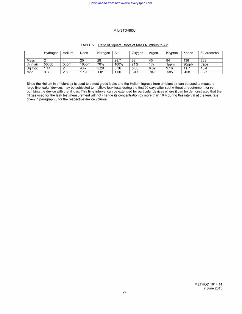
MIL-STD-883J
METHOD 1014.14 7 June 2013
27
TABLE VI. Ratio of Square Roots of Mass Numbers to Air.
Hydrogen Helium Neon Nitrogen Air Oxygen Argon Krypton Xenon Fluorocarbo
nMass 2 4 20 28 28.7 32 40 84 136 269% in air 50ppb 5ppm 18ppm 78% 100% 21% 1% 1ppm 90ppb traceSq root 1.41 2 4.47 5.29 5.36 5.66 6.32 9.16 11.7 16.4ratio 3.80 2.68 1.19 1.01 1.00 .947 .848 .585 .458 .327
Since the Helium in ambient air is used to detect gross leaks and the Helium ingress from ambient air can be used to measure large fine leaks, devices may be subjected to multiple leak tests during the first 60 days after seal without a requirement for re-bombing the device with the fill gas. This time interval can be extended for particular devices where it can be demonstrated that the fill gas used for the leak test measurement will not change its concentration by more than 10% during this interval at the leak rate given in paragraph 3 for the respective device volume.
Downloaded from http://www.everyspec.com
MIL-STD-883J
METHOD 1014.14 7 June 2013
28
2.8.6.2 CHLD bombing with gasses other than Helium fine/gross leak combination.
2.8.6.2.1 Apparatus. CHLD system as in 2.8.2.
2.8.6.2.2. Procedure. As in CH2, 2.8.5 except that when using the Howl-Mann equation (2.1.2.3), the fixed value 2.69 (MA/M
which is the ratio of the square roots for Helium) should be replaced with the appropriate ratio from Table VI for the tracer gas being used to bomb the devices. The gross leak rate is determined by sensing the ingress of Helium from ambient air into the device and therefore leak tests should not be conducted in less than 60 minutes from the time a device is removed from the bombing chamber. This time interval is necessary to allow a sufficient gas exchange to occur within the device between the tracer gas (in this case not Helium) and ambient air so that gross leaks can be detected. In some cases, surface desorption effects of the tracer gas will have to be characterized and mitigated as in 2.8.3.1.1.
2.8.6.3 CHLD re-screening devices gross leak tested with Fluorocarbons. It has been demonstrated that a Helium fine leak measurement can be skewed by as much as one order of magnitude if the leak path is plugged by a Fluorocarbon fluid typically used for the bubble test or gross leak test. When re-screening legacy devices, it may be advantageous to bomb the devices with Helium and then conduct a leak test as in 2.8.5 where the leak rate of Helium is measured simultaneously with the measurement of Fluorocarbons left over from the previous bubble test.
2.8.6.3.1 Apparatus. CHLD system as in 2.8.6.1.1.
2.8.6.3.2 Procedure. As in 2.8.6.2.2 where the Fluorocarbon leak rate is used on a relative basis to determine whether devices are in “Family”. Previous tests have indicated a noticeable difference between devices which have plugged leak paths and fine leaks. Since the fine leak rate can be expected to be skewed to a lower measured leak rate in an unpredictable manner, the interpretation of the test results must be made on a case by case basis and validated by conducting IGA analysis on selected devices. This measurement process has produced prediction results of 100% for “good” devices and 95% for “bad” devices (devices which contain large concentrations of Fluorocarbons in addition to large amounts of water when subjected to the Test Method 1018 for IGA). The 5% false “bad” prediction rate comes from the inability to determine whether the Fluorocarbons are coming from a plugged leak path or from surface porosity or other mechanical defect which does not extend into the hermetic cavity. It has also been demonstrated that if devices are subjected to a 100 ºC bake out in a 1 X 10⁻⁶ Torr vacuum chamber for 72 hours prior to bombing and leak testing, the effects of Fluorocarbon plugging becomes a non-issue.
2.8.6.4 Package volume and leak rate limits for condition Z. Leak rate range limits are the same as condition CH, and are dependent on the performance of an individual test system, but an expected typical range would be from the gross leak as defined in condition CH, 2.8.5.1 to 1.0 X 10⁻¹⁰ atm-cc/sec for tracer gasses other than Helium.
2.8.6.5 Failure criteria. The failure criteria for Fine Leak is provided in Table VII of paragraph 3.
Downloaded from http://www.everyspec.com
MIL-STD-883J
METHOD 1014.14 7 June 2013
29
2.8.7 Summary. The following conditions shall be specified in the applicable performance specification:
a. Test condition letter when a specific test is to be applied (see 1.3.).
b. Accept or reject leak rate for test conditions CH1, CH2, or Z when other than the accept or reject leak rate specified
herein applies (see Table VII of paragraph 3).
2.8.8 Notes.
1. Any device that has been subjected to Fluorocarbon leak testing will then interfere with subsequent dry gas leak testing. This is most noticeable with helium leak testing as it is known to reduce the measured leak rate by at least one order of magnitude. The devices may be tested per 2.8.6.2.or 2.8.6,3 using out of family criteria, however, these tests must be validated on a case by case basis using IGA test Method 1018 on select devices provided that the lot of devices is large enough to support the validation tests.
2. When retesting devices to test condition H1, H2 or CH, the history of device exposure to helium including dates,
backfilling performed, tracer gas concentrations, pressure, and time exposed, should be known in order to ensure reliable results. The sum of the bombing times and the total dwell time from the first bombing interval to the expected subsequent leak test can be used in the Howl-Mann equation to compute a new R1 value if no Helium was sealed in the device. Whenever parts are sealed in helium or prior helium testing may have been performed on a device, the internal helium content can be calculated from the following formula (see Eq (8)):
QHe-total = QHe + pi(e-(
L
He t/V) )
Where: QHe-total = the total Helium contained in the package at the time of test pi = the atmospheres of Helium sealed within the device LHe = the true Helium leak rate t = the time between seal and test V = the internal volume of the device in cm3. QHe = the amount of Helium forced into the device during bombing
QHe = {PE-[ pi(e-( L
He t/V) )]}(1 - e-( L
He t/V) )
Where: PE = bombing pressure in absolute atmospheres T = the bombing time in seconds
Once QHe-total is known, the leak rate test limit (R1) can be determined from 2.8.6.1.2 Equation (6).
3. Any device detected as a marginal reject using test condition CH and no leak testing history is available can be retested using a different dry gas medium as in 2.8.6.2.
4. If the history of the device indicates that it has been subjected to fluorocarbon fluid testing, or if there is no history
evidencing that it has not been, then the device must be assumed to have fluorocarbon contamination and the recommendations of 2.8.8. Note 3 must be followed or the device tested per 2.8.6.2 or 2.8.6.3.
Eq (9)
Eq (8)
Downloaded from http://www.everyspec.com
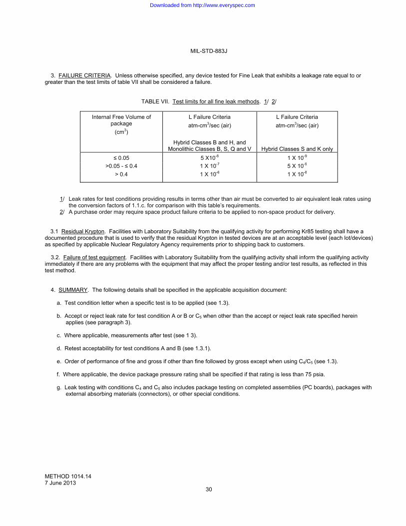
MIL-STD-883J
METHOD 1014.14 7 June 2013
30
3. FAILURE CRITERIA. Unless otherwise specified, any device tested for Fine Leak that exhibits a leakage rate equal to or
greater than the test limits of table VII shall be considered a failure.
TABLE VII. Test limits for all fine leak methods. 1/ 2/
Internal Free Volume of package
(cm3)
L Failure Criteria
atm-cm3/sec (air)
Hybrid Classes B and H, and Monolithic Classes B, S, Q and V
L Failure Criteria
atm-cm3/sec (air)
Hybrid Classes S and K only
≤ 0.05 5 X10⁻⁸ 1 X 10⁻⁹
>0.05 - ≤ 0.4 1 X 10⁻⁷ 5 X 10⁻⁹
> 0.4 1 X 10⁻⁶ 1 X 10⁻⁸
1/ Leak rates for test conditions providing results in terms other than air must be converted to air equivalent leak rates using the conversion factors of 1.1.c. for comparison with this table’s requirements.
2/ A purchase order may require space product failure criteria to be applied to non-space product for delivery.
3.1 Residual Krypton. Facilities with Laboratory Suitability from the qualifying activity for performing Kr85 testing shall have a documented procedure that is used to verify that the residual Krypton in tested devices are at an acceptable level (each lot/devices) as specified by applicable Nuclear Regulatory Agency requirements prior to shipping back to customers.
3.2. Failure of test equipment. Facilities with Laboratory Suitability from the qualifying activity shall inform the qualifying activity immediately if there are any problems with the equipment that may affect the proper testing and/or test results, as reflected in this test method.
4. SUMMARY. The following details shall be specified in the applicable acquisition document:
a. Test condition letter when a specific test is to be applied (see 1.3). b. Accept or reject leak rate for test condition A or B or C5 when other than the accept or reject leak rate specified herein
applies (see paragraph 3). c. Where applicable, measurements after test (see 1 3). d. Retest acceptability for test conditions A and B (see 1.3.1). e. Order of performance of fine and gross if other than fine followed by gross except when using C4/C5 (see 1.3). f. Where applicable, the device package pressure rating shall be specified if that rating is less than 75 psia. g. Leak testing with conditions C4 and C5 also includes package testing on completed assemblies (PC boards), packages with
external absorbing materials (connectors), or other special conditions.
Downloaded from http://www.everyspec.com
MIL-STD-883J
METHOD 1015.10 26 February 2010
1
METHOD 1015.10 BURN-IN TEST
1. PURPOSE. The burn-in test is performed for the purpose of screening or eliminating marginal devices, those with inherent defects or defects resulting from manufacturing aberrations which cause time and stress dependent failures. In the absence of burn-in, these defective devices would be expected to result in infant mortality or early lifetime failures under use conditions. Therefore, it is the intent of this screen to stress microcircuits at or above maximum rated operating conditions or to apply equivalent screening conditions, which will reveal time and stress dependent failure modes with equal or greater sensitivity.
2. APPARATUS. Details for the required apparatus shall be as described in method 1005.
3. PROCEDURE. The microelectronic device shall be subjected to the specified burn-in screen test condition (see 3.1) for the time and temperature specified (see method 5004 for the appropriate device class level) or, unless otherwise specified, for an equivalent time and temperature combination as determined from table I (see 3.1.1 and 3.1.2). QML manufacturers who are certified and qualified to MIL-PRF-38535 may modify the time or the temperature condition independently from the regression conditions contained in table I or the test condition/circuit specified in the device specification or standard microcircuit drawing provided the modification is contained in the manufacturers Quality Management Plan and the “Q" certification identifier is marked on the devices. Any time-temperature combination which is contained in table I for the appropriate class level may be used for the applicable test condition. The test conditions (duration and temperature) selected prior to test shall be recorded and shall govern for the entire test. Lead-, stud-, or case-mounted devices shall be mounted by the leads, stud, or case in their normal mounting configuration, and the point of connection shall be maintained at a temperature not less than the specified ambient temperature. Pre and post burn-in measurements shall be made as specified. Burn-in boards shall not employ load resistors which are common to more than one device, or to more than one output pin on the same device.
3.1 Test conditions. Basic test conditions are as shown below. Unless otherwise specified, test condition F shall not be applied to class level S devices. Details of each of these conditions, except where noted, shall be as described in method 1005.
a. Test condition A: Steady-state, reverse bias. b. Test condition B: Steady-state, forward bias. c. Test condition C: Steady-state, power and reverse bias. d. Test condition D: Parallel excitation. e. Test condition E: Ring oscillator. f. Test condition F: Temperature-accelerated test.
3.1.1 Test temperature. The ambient burn-in test temperature shall be 125C minimum for conditions A through E (except for hybrids see table I). At the supplier's option, the test temperature for conditions A through E may be increased and the test time reduced in accordance with table I. Since case and junction temperature will, under normal circumstances, be significantly higher than ambient temperature, the circuit employed should be so structured that maximum rated junction temperature for test or operation shall not exceed 200°C for class level B or 175°C for class level S (see 3.1.1.1). Devices with internal thermal shut-down circuitry shall be handled in accordance with 3.2.3 of method 1005. The specified test temperature is the minimum actual ambient temperature to which all devices in the working area of the chamber shall be exposed. This shall be assured by making whatever adjustments are necessary in the chamber profile, loading, location of control or monitoring instruments, and the flow of air or other suitable gas or liquid chamber medium. Therefore, calibration shall be accomplished on the chamber in a fully loaded (boards need not be loaded with devices), unpowered configuration, and the indicator sensor located at, or adjusted to reflect the coldest point in the working area.
Downloaded from http://www.everyspec.com
MIL-STD-883J
METHOD 1015.10 26 February 2010
2
3.1.1.1 Test temperature for high power devices. Regardless of power level, devices shall be able to be burned in or
life-tested at their maximum rated operating temperature. For devices whose maximum operating temperature is stated in terms of ambient temperature, TA, table I applies. For devices whose maximum operating temperature is stated in terms of case temperature, TC and where the ambient temperature would cause TJ to exceed +200°C (+175°C for class level S), the ambient operating temperature may be reduced during burn-in and life test from +125°C to a value that will demonstrate a TJ between +175°C and +200°C and TC equal to or greater than +125°C without changing the test duration. Data supporting this reduction shall be available to the acquiring and qualifying activities upon request.
3.1.1.2 Test temperature for hybrid devices. The ambient or case burn-in test temperature shall be as specified in table I, except case temperature burn-in shall be performed, as a minimum, at the maximum operating case temperature (TC) specified for the device. Burn-in shall be 320 hours minimum for class level S hybrids (class K). The device should be burned in at the maximum specified operating temperature, voltage, and loading conditions as specified in the device specification or drawing. Since case and junction temperature will, under normal circumstances, be significantly higher than ambient temperature, the circuit should be so structured that the maximum rated junction temperature as specified in the device specification or drawing, and the cure temperature of polymeric materials as specified in the baseline documentation shall not be exceeded. If no maximum junction temperature is specified, a maximum of 175°C is assumed. Accelerated burn-in (condition F) shall not be permitted. The specified test temperature shall be the minimum actual ambient or case temperature that must be maintained for all devices in the chamber. This shall be assured by making whatever adjustments are necessary in the chamber profile, loading, location of control or monitoring instruments and the flow of air or other suitable gas or liquid chamber medium.
3.1.2 Temperature accelerated test details. In test condition F, microcircuits are subjected to bias(es) at a temperature (175°C to 250°C) which considerably exceeds the maximum rated junction temperature. At these elevated temperatures, it is generally found that microcircuits will not operate normally as specified in their applicable acquisition documents, and it is therefore necessary that special attention be given to the choice of bias circuits and conditions to assure that important circuit areas are adequately biased without subjecting other areas of the circuit to damaging overstress(es). To properly select the accelerated test conditions, it is recommended that an adequate sample of devices be exposed to the intended high temperature while measuring voltage(s) and current(s) at each device terminal to assure that the applied electrical stresses do not induce damaging overstress. Unless otherwise specified in the device specifications or drawings, the minimum time-temperature combination shall be as delineated by table I. The minimum test time shall be 12 hours. The applied voltage at any or all terminals shall be equal to the recommended operating voltage(s) at 125°C. When excessive current flow or power dissipation would result from operation at the specified voltage(s), the applied voltage(s) at any or all terminals may be reduced to a minimum of 50 percent of the specified voltage(s) and the testing time shall be determined in accordance with the formula given in 3.5.6 of method 1005. Devices with internal thermal shut-down circuitry shall be handled in accordance with 3.5.6.1 of method 1005. Thermal runaway conditions must be avoided at all times.
3.2 Measurements. Pre burn-in measurements, when specified, or at the manufacturer's discretion when not specified, shall be conducted prior to applying burn-in test conditions. Post burn-in measurements shall be completed within 96 hours after removal of the devices from the specified burn-in test condition (i.e., either removal of temperature or bias) and shall consist of all 25°C dc parameter measurements) (subgroup A-1 of method 5005, or subgroups tested in lieu of A-1 as allowed in the most similar military device specification or standard microcircuit drawing) and all parameters for which delta limits have been specified as part of interim (post-burn-in) electrical measurements. Delta limit acceptance, when applicable, shall be based upon these measurements. If these measurements cannot be completed within 96 hours, for either the standard or accelerated burn-in, the devices shall be subjected to the same test condition (see 3.1) and temperature previously used for a minimum additional reburn-in time as specified in table I before post burn-in measurements are made.
3.2.1 Cooldown after standard burn-in. All devices shall be cooled to within 10°C of their power stable condition at room temperature prior to the removal of bias. The interruption of bias for up to 1 minute for the purpose of moving the devices to cooldown positions separate from the chamber within which burn-in testing was performed shall not be considered removal of bias, (bias at cooldown position shall be same as that used during burn-in). Alternatively, except for linear or MOS (CMOS, NMOS, PMOS, etc.) devices or unless otherwise specified, the bias may be removed during cooling provided the case temperature of devices under test is reduced to a maximum of 35°C within 30 minutes after the removal of the test conditions and provided the devices under test are removed from the heated chamber within 5 minutes following removal of bias. All 25°C dc measurements or alternate subgroups (see 3.2) shall be completed prior to any reheating of the device(s).
Downloaded from http://www.everyspec.com
MIL-STD-883J
METHOD 1015.10 26 February 2010
3
3.2.2 Cooldown after accelerated burn-in. All devices subjected to the accelerated testing of condition F shall be cooled
to within 10°C of power stable at room temperature prior to the removal of bias. Interruption of bias for a period of up to 1 minute for the purpose of moving devices to cooldown positions separate from the chamber within which burn-in was conducted shall not be considered removal of bias, (bias at cooldown position shall be same as that used during burn-in). All specified 25°C dc electrical measurements shall be completed prior to any reheating of the devices.
3.2.3 Test setup monitoring. The test setup shall be monitored at the test temperature initially and at the conclusion of the test to establish that all devices are being stressed to the specified requirements. The following is the minimum acceptable monitoring procedure:
a. Device sockets. Initially and at least each 6 months thereafter, (once every 6 months or just prior to use if not used
during the 6 month period) each test board or tray shall be checked to verify continuity to connector points to assure that bias supplies and signal information will be applied to each socket. Board capacitance or resistance required to ensure stability of devices under test shall be checked during these initial and periodic verification tests to ensure they will perform their proper function (i.e., that they are not open or shorted). Except for this initial and periodic verification, each device or device socket does not have to be checked; however, random sampling techniques shall be applied prior to each time a board is used and shall be adequate to assure that there are correct and continuous electrical connections to the devices under test.
b. Connectors to test boards or trays. After the test boards are loaded with devices, inserted into the oven, and brought
up to at least 125°C (or the specified test temperature, if less than 125°C) each required test voltage and signal condition shall be verified in at least one location on each test board or tray so as to assure electrical continuity and the correct application of specified electrical stresses for each connection or contact pair used in the applicable test configuration. This shall be performed by opening the oven for a maximum of 10 minutes.
c. At the conclusion of the test period, prior to removal of devices from temperature and test conditions, the voltage and
signal condition verification of b above shall be repeated. d. For class level S devices, each test board or tray and each test socket shall be verified prior to test to assure that the
specified test conditions are applied to each device. This may be accomplished by verifying the device functional response at each device output(s). An approved alternate procedure may be used.
Where failures or open contacts occur which result in removal of the required test stresses for any period of the required test duration (see 3.1), the test time shall be extended to assure actual exposure for the total minimum specified test duration. Any loss(es) or interruption(s) of bias in excess of 10 minutes total duration while the chamber is at temperature during the final 8 hours of burn-in shall require extension of the test duration for an uninterrupted 8 hours minimum, after the last bias interruption.
4. SUMMARY. The following details shall be specified in the applicable acquisition document:
a. Test duration if other than as defined for the applicable class level in method 5004, or time-temperature combination shown in table I.
b. Test condition letter. c. Burn-in test temperature, and whether ambient, junction, or case (see 3), if other than as specified in 3.1.1. d. Test mounting, if other than normal (see 3). e. Pre and post burn-in measurements and drift limits, as applicable (see 3.2). f. Authorization for use of condition F and special maximum test rating for condition F (see 3.1 and 3.1.2), when
applicable. g. Time within which post burn-in measurements must be completed if other than specified (see 3.2).
Downloaded from http://www.everyspec.com
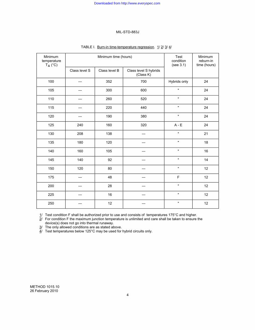
MIL-STD-883J
METHOD 1015.10 26 February 2010
4
TABLE I. Burn-in time-temperature regression. 1/ 2/ 3/ 4/
Minimum temperature
TA (°C)
Minimum time (hours) Test condition (see 3.1)
Minimum reburn-in
time (hours) Class level S Class level B Class level S hybrids
(Class K)
100 --- 352 700 Hybrids only 24
105 --- 300 600 " 24
110 --- 260 520 " 24
115 --- 220 440 " 24
120 --- 190 380 " 24
125 240 160 320 A - E 24
130 208 138 --- " 21
135 180 120 --- " 18
140 160 105 --- " 16
145 140 92 --- " 14
150 120 80 --- " 12
175 --- 48 --- F 12
200 --- 28 --- " 12
225 --- 16 --- " 12
250 --- 12 --- " 12
1/ Test condition F shall be authorized prior to use and consists of temperatures 175°C and higher. 2/ For condition F the maximum junction temperature is unlimited and care shall be taken to ensure the device(s) does not go into thermal runaway. 3/ The only allowed conditions are as stated above. 4/ Test temperatures below 125°C may be used for hybrid circuits only.
Downloaded from http://www.everyspec.com
MIL-STD-883J
METHOD 1016.2 26 February 2010
1
METHOD 1016.2 LIFE/RELIABILITY CHARACTERIZATION TESTS 1. PURPOSE. The purpose of the life characterization tests is to determine: (1) the life distributions, (2) the life acceleration characteristics, and (3) the failure rate (λ) potential of the devices. For a discussion of failure rates and life test considerations, see MIL-HDBK-217. Failure rates are ordinarily determined either for general qualification of devices or the production lines from which they are obtained or for the purpose of predicting the failure rates (or Mean Time Between Failure (MTBF)) of equipments in which the devices are to be employed. NOTE: A detailed dissertation on the life test result analysis techniques, with application examples, is presented by D.S.
Peck in the Proceedings of the 9th Annual Reliability Physics Symposium (1971), pages 69 through 78. Further improvements to the methods of test result analysis are possible by using computer aided techniques such as regression analysis and iterative curve fitting.
2. APPARATUS. Suitable sockets or other mounting means shall be provided to make firm electrical contact to the terminals of devices under test in the specified circuit configuration. The mounting means shall be so designed that they will not remove internally dissipated heat from the device by conduction, other than that removed through the device terminals and the necessary electrical contacts, which shall be maintained at or above the specified ambient temperature. The apparatus shall provide for maintaining the specified biases at the terminal(s) of the device under test and, when specified, monitoring of the input excitation. Power supplies and current-setting resistors shall be capable of maintaining the specified operating conditions, as minima, throughout the testing period with normal variations in their source voltages, ambient temperatures, etc. The test equipment shall preferably be so arranged that only natural-convection cooling of the devices occurs. When test conditions result in significant power dissipation, the test apparatus shall be arranged so as to result in the approximate average power dissipation for each device whether devices are tested individually or in a group. The test circuits need not compensate for normal variations in individual device characteristics but shall be arranged so that the existence of failed or abnormal (i.e., open, short, etc.) devices in a group does not negate the effect of the test for other devices in the group. 3. PROCEDURE. The microelectronic devices shall be subjected to the specified test condition (see 3.4) for the specified duration and test temperature, and the required measurements shall be made at the specified intermediate points and endpoints. Lead-, stud-, or case-mounted devices shall be mounted by the leads, stud, or case in their normal mounting configuration, and the point of connection shall be maintained at a temperature not less than the specified temperature. The test condition, duration, sample size, and temperature selected prior to test shall be recorded and shall govern for the entire test. 3.1 Test duration. The life test duration shall be as follows: Initial qualification: 4,000 (+72, -240) hours or 75 percent failures, whichever comes first All other tests: 1,000 (+72, -24) hours or 50 percent failures, whichever comes first Within the time interval of 24 hours before to 72 hours after the specified duration of the test, the devices shall be removed from the specified test conditions and allowed to reach standard test conditions prior to the removal of bias. 3.2 Measurements. Measurements shall be grouped into two categories as follows: Type A: Initial and final measurement. Type B: Interim measurements.
Downloaded from http://www.everyspec.com
MIL-STD-883J
METHOD 1016.2 26 February 2010
2
Unless otherwise specified, all measurements shall be completed within 8 hours after removal of the device from the specified test conditions and shall consist of the following: Type A: All specified endpoint measurement. Type B: Selected critical parameters (see 4). The type A measurements shall be made at the zero hour and final measurement time. The type B interim measurements shall be made at the 4, 8, 16, 32, 64, 128, 256, 512 hour times for the 1000 hour test and additionally, at 1000, and 2000 hour times for the 4000 hour test. 3.2.1 Measurements following life test. When devices are measured following application of life test conditions, they shall be cooled to room temperature prior to the removal of bias. All specified 25°C electrical measurements shall be completed prior to any reheating of the devices. 3.2.2 Test setup monitoring. The test setup shall be monitored at the test temperature initially and at the conclusion of the test to establish that all devices are being stressed to the specified requirements. The following is the minimum acceptable monitoring procedure:
a. Device sockets. Initially and at least each 6 months thereafter, each test board or tray shall be checked to verify
continuity to connector points to assure that bias supplies and signal information will be applied to each socket. Except for this initial and periodic verification, each device or device socket does not have to be checked; however, random sampling techniques shall be applied prior to each time a board is used and shall be adequate to assure that there are correct and continuous electrical connections to the devices under test.
b. Connectors to test boards or trays. After the test boards are loaded with devices, inserted into the oven, and brought
up to at least 125°C or the specified test temperature, whichever is less, each required test voltage and signal condition shall be verified in at least one location on each test board or tray so as to assure electrical continuity and the correct application of specified electrical stresses for each connection or contact pair used in the applicable test configuration. This may be performed by opening the oven for a maximum of 10 minutes.
c. At the conclusion of the test period, prior to removal of devices from temperature and test conditions, the voltage and
signal condition verification of b above shall be repeated.
d. For class level S devices when loading boards or trays the continuity between each device and a bias supply shall be verified.
Where failures or open contacts occur which result in removal of the required test stresses for any period of the required test duration, the test time shall be extended to assure actual exposure for the total minimum specified test duration. 3.3 Test sample. The test sample shall be as specified (see 4). No fewer than 40 devices shall be specified for a given test temperature. 3.4 Test conditions. In this condition microcircuits are subjected to bias(es) at temperatures (200C to 300C) which considerably exceed the maximum rated operating temperature. At these elevated temperatures, it is generally found that microcircuits will not operate normally as specified in their applicable acquisition document and it is therefore necessary that special attention be given to the choice of bias circuits and conditions to assure that important circuit areas are adequately biased, without damaging overstress of other areas of the circuit.
Downloaded from http://www.everyspec.com
MIL-STD-883J
METHOD 1016.2 26 February 2010
3
3.4.1 Test temperatures. Unless otherwise specified, test temperatures shall be selected in the range of 200C to 300C. The specified test temperature is the minimum actual ambient temperature to which all devices in the working area of the chamber shall be exposed. This shall be assured by making whatever adjustments are necessary in the chamber profile, loading, location of control or monitoring instruments, and the flow of air or other chamber atmosphere. Therefore, calibration shall be accomplished on the chamber in a fully loaded, unpowered configuration, and the indicator sensor located at, or adjusted to reflect the coldest point in the working area. For the initial failure rate determination test, three temperatures shall be selected. A minimum of 25°C separation shall be maintained between the adjacent test temperatures selected. All other periodic life tests shall be conducted with two temperatures and a minimum of 50°C separation. 3.4.2 Bias circuit selection. To properly select the accelerated test conditions, it is recommended that an adequate sample of devices be exposed to the intended high temperature while measuring voltage(s) and current(s) at each device terminal to assure that the applied electrical stresses do not induce damage. Therefore, prior to performing microcircuit life tests, test circuit, thermal resistance (where significant), and step-stress evaluations should be performed over the test ranges, usually 200°C to 300°C. Steps of 25°C for 24 hours minimum duration (all steps of equal duration with a tolerance of no greater than ±5 percent), each followed by proper electrical measurements, shall be used for step-stress tests. Optimum test conditions are those that provide maximum voltage at high thermal stress to the most failure-prone junctions or sites, but maintain the device current at a controlled low level. Excessive device current may lead to thermal runaway (and ultimately device destruction). Current-limiting resistors shall be employed. The applied voltage at any or all terminal(s) shall be equal to the maximum rated voltage at 125°C. If necessary, only with the specific approval of the qualifying activity, the applied voltage at any or all terminals(s) may be reduced to not less than 50 percent of the specified value(s) when it is demonstrated that excessive current flow or power dissipation would result from operation at the specified voltage(s). If the voltage(s) is so reduced, the life testing time shall be determined in accordance with the formula given in 3.5.6 of method 1005. 3.5 Life test ground rules. As an aid to selecting the proper test conditions for an effective microcircuit accelerated life or screening test, the following rules have been formulated:
a. Apply maximum rated voltage (except as provided in 3.4.2) to the most failure prone microcircuit sites or junctions identified during step-stress evaluation.
b. Apply electrical bias to the maximum number of junctions. c. In each MOS or CMOS device, apply bias to different gate oxides so that both positive and negative voltages are
present. d. Control device currents to avoid thermal runaway and excessive electromigration failures. e. Employ current-limiting resistors in series with each device to ensure the application of electrical stress to all
nonfailed devices on test. f. Select a value of each current-limiting resistor large enough to prevent massive device damage in the event of
failure, but small enough to minimize variations in applied voltage due to current fluctuations. g. Avoid conditions that exceed design or material limitations such as solder melting points. h. Avoid conditions that unduly accelerate nontypical field condition failure-mechanisms. i. Employ overvoltage protection circuitry.
The determination of test conditions that conform to the established ground rules involves three basic steps: (1) evaluation of candidate bias circuits at accelerated test temperatures, (2) device thermal characterization, and (3) the performance of step-stress tests.
Downloaded from http://www.everyspec.com
MIL-STD-883J
METHOD 1016.2 26 February 2010
4
3.6 Test results analysis. Failure analysis of the accelerated test results is necessary to separate the failures into temperature and nontemperature dependent categories. The nontemperature dependent failures should be removed from the test data prior to life distribution analysis. All failures shall be reported together with the analysis results and rationale for deletion of those identified as nontemperature dependent. 3.6.1 Life distribution analysis. The effectiveness of the test result analysis can be enhanced by diligent failure analysis of each test failure. Failures should be grouped by similarity of failure mechanisms, that is, surface related, metal migration, intermetallic formation, etc. The time-to-failure history of each failure in a group should be recorded. This includes the individual failure times and the associated calculated cumulative percent failures. To facilitate estimating the distribution parameters from small-sample life tests, the data is plotted as a cumulative distribution. Since semiconductor life distributions have been shown to follow a lognormal distribution, graph paper similar to figure 1016-1 is required for data analysis. The lognormal distribution will appear as a straight line on this paper. The expected bimodal distribution of "freak" and "main" populations in a combined form normally appears as an s-shaped plot. The distribution parameters necessary for data analysis, median life and sigma (σ) can be calculated as:
lntime of failure
time of failure
50%
16%
Separate analysis of the individual "freak" and "main" populations should be performed and "goodness of fit" tests applied to test the apparent distribution(s). 3.6.2 Life acceleration analysis. Life/reliability characterization requires the establishing of failure distributions for several temperature stress levels at the same rated voltage condition. These failure distributions must represent a common failure mechanism. Using a specially prepared graph paper for Arrhenius Reaction Rate Analysis as shown in figure 1016-2, the median life times for the "freak" and "main" populations can be plotted to determine equivalent life-times at the desired use temperatures. 3.6.3 Failure rate calculations. Semiconductor failures are lognormally distributed. Therefore, the failure rate will vary with time. Semiconductor failure rates at any given time can be calculated using figure 1016-3 which is a normalized presentation of the mathematical calculations for the instantaneous failure rate from a lognormal distribution. 4. SUMMARY. The following details shall be as specified in the applicable acquisition document:
a. Test temperature(s) and whether ambient or case.
b. Test mounting if other than normal (see 3).
c. Endpoint measurements (see 3.2).
d. Intermediate measurements (see 3.2).
e. Criteria for failure for endpoint and intermediate measurements (see 3.2), if other than device specification limits.
f. Test sample (see 3.3).
g. Requirements for inputs, outputs, biases, test circuit, and power dissipation, as applicable (see 3.4).
Downloaded from http://www.everyspec.com
MIL-STD-883J
METHOD 1016.2 26 February 2010
5
h. Requirements for data analysis, including: (1) Failure analysis results. (2) Data calculations: (a) Log normal by temperature. (b) Reaction rate relationships (c) Failure rate versus time.
Downloaded from http://www.everyspec.com
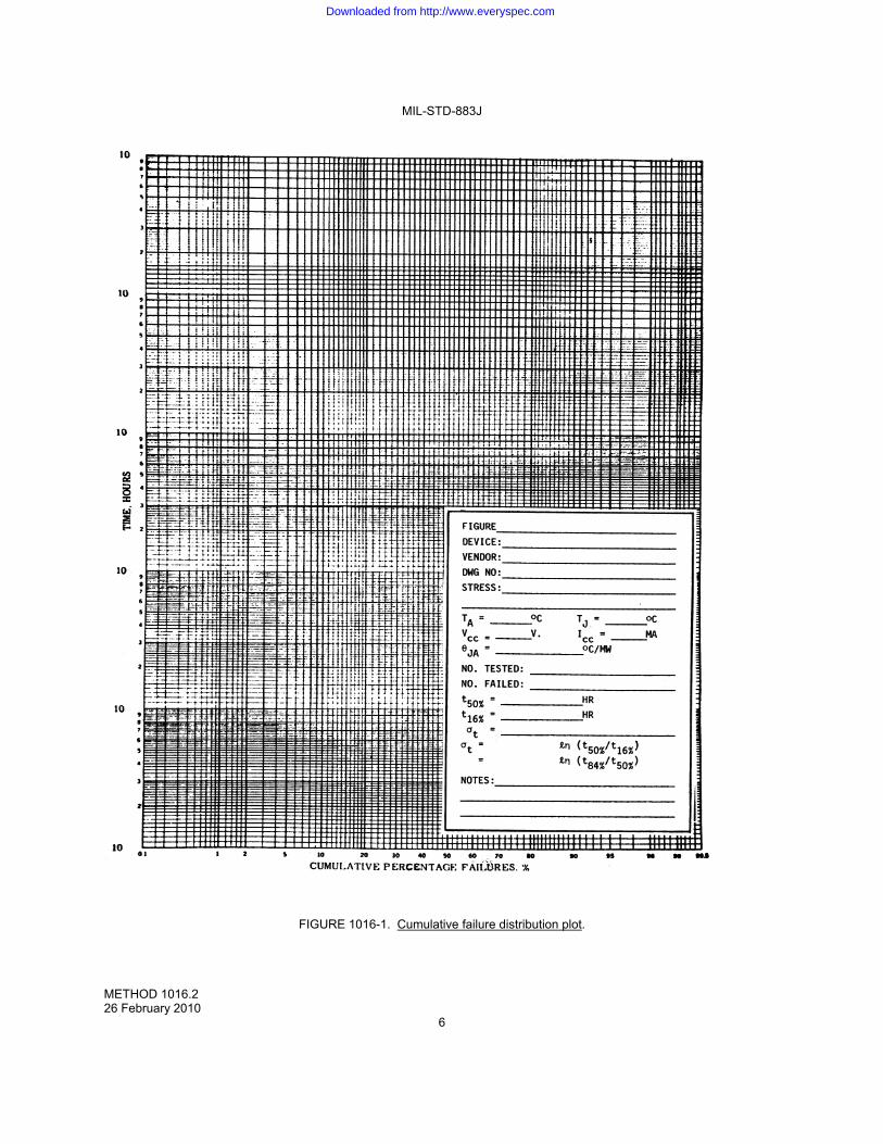
MIL-STD-883J
METHOD 1016.2 26 February 2010
6
FIGURE 1016-1. Cumulative failure distribution plot.
Downloaded from http://www.everyspec.com
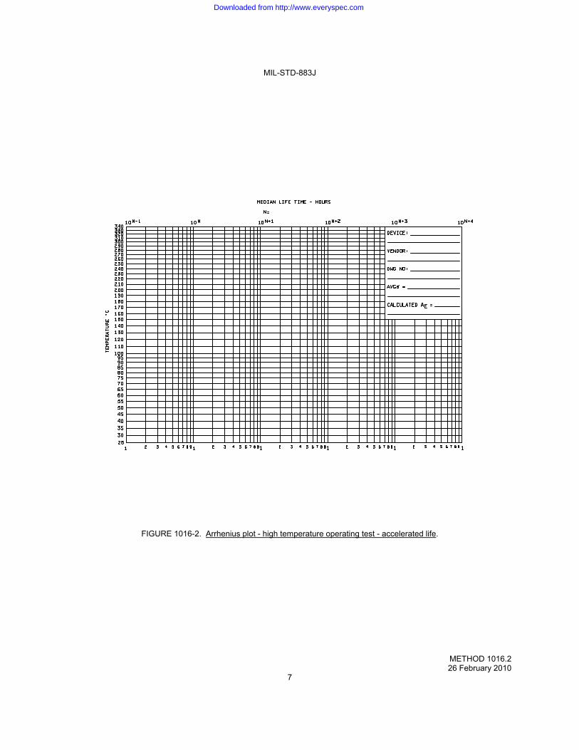
MIL-STD-883J
METHOD 1016.2 26 February 2010
7
FIGURE 1016-2. Arrhenius plot - high temperature operating test - accelerated life.
Downloaded from http://www.everyspec.com
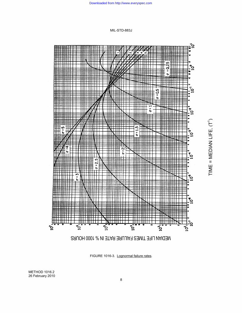
MIL-STD-883J
METHOD 1016.2 26 February 2010
8
FIGURE 1016-3. Lognormal failure rates.
TIM
E =
ME
DIA
N L
IFE
, (T
1 )
Downloaded from http://www.everyspec.com
MIL-STD-883J
METHOD 1017.3 7 June 2013
1
METHOD 1017.3 NEUTRON IRRADIATION 1. PURPOSE. The neutron irradiation test is performed to determine the susceptibility of semiconductor devices to non-ionizing energy loss (NIEL) degradation. The tests described herein are applicable to integrated circuits, transistors, and diodes. This is a destructive test. Objectives of the test are: (1) to detect and measure the degradation of critical semiconductor device parameters as a function of neutron fluence, and (2) to determine if specified semiconductor device parameters are within specified limits after exposure to a specified level of neutron fluence (see section 4). 2. APPARATUS. 2.1 Test instruments. Test instrumentation to be used in the radiation test shall be standard laboratory electronic test instruments such as power supplies, digital voltmeters, and picoammeters, etc., capable of measuring the electrical parameters required. Parameter test methods and calibration shall be in accordance with MIL-STD-883 or MIL-STD-750, whichever is applicable.
2.2 Radiation source. The radiation source used in the test shall be a well characterized neutron source that produces either a broad neutron energy spectrum (such as a TRIGA Reactor or a Fast Burst Reactor) or a monoenergetic neutron spectrum such as available from DT or DD accelerators) provided that the output can be converted to a 1 MeV equivalent spectrum using Department of Defense adopted ASTM standards. The uncertainty in the neutron spectrum shall be characterized in the form of an energy-dependent covariance matrix. The neutron source shall be characterized for the associated ionizing radiation production per unit of neutron fluence prior to use. Facilities that generate more than 500 rad(Si) of Total Ionizing Dose (TID) per 1 X 10¹² n/cm3 (1 MeV equivalent) shall not be used. The source shall be one that is acceptable to the acquiring activity.
a. Operation may be in either pulse or steady-state mode as appropriate.
2.3 Dosimetry equipment (as required).
a. Fast-neutron threshold activation foils such as 32S, 54Fe, and 58Ni. b. CaF2 thermoluminescence dosimeters (TLDs). c. Appropriate activation foil counting and TLD readout equipment.
2.4 Dosimetry measurements. 2.4.1 Neutron fluences. The neutron fluence used for device irradiation shall be obtained by measuring the amount of radioactivity induced in a fast-neutron threshold activation foil such as 32S, 54Fe, or 58Ni, irradiated simultaneously with the device. A standard method for converting the measured radioactivity in the specific activation foil employed into a neutron fluence is given in the following Department of Defense adopted ASTM standards: ASTM E 263 Standard Test Method for Measuring Fast-Neutron Reaction Rates by Radioactivation
of Iron. ASTM E 264 Standard Test Method for Measuring Fast-Neutron Reaction Rates by Radioactivation
of Nickel. ASTM E 265 Standard Test Method for Measuring Fast-Neutron Reaction Rates by Radioactivation
of Sulfur.
*
*
*
*
*
Downloaded from http://www.everyspec.com
MIL-STD-883J
METHOD 1017.3 7 June 2013
2
The conversion of the foil radioactivity into a neutron fluence requires a knowledge of the neutron spectrum incident on the foil. If the spectrum is not known, it shall be determined by use of the following DoD adopted ASTM standards, or their equivalent: ASTM E 720 Standard Guide for Selection of a Set of Neutron-Activation Foils for Determining
Neutron Spectra used in Radiation-Hardness Testing of Electronics. ASTM E 721 Standard Method for Determining Neutron Energy Spectra with Neutron-Activation
Foils for Radiation-Hardness Testing of Electronics. ASTM E 722 Standard Practice for Characterizing Neutron Energy Fluence Spectra in Terms of an
Equivalent Monoenergetic Neutron Fluence for Radiation-Hardness Testing of Electronics.
ASTM E 1018 Standard Guide for Application of ASTM Evaluated Cross Section Data File. Once the neutron energy spectrum has been determined and the equivalent monoenergetic fluence calculated, then an appropriate monitor foil (such as 32S, 54Fe, or 58Ni) should be used in subsequent irradiations to determine the neutron fluence as discussed in ASTM E 722. Thus, the neutron fluence is described in terms of the equivalent monoenergetic neutron fluence per unit monitor response. Use of a monitor foil to predict the equivalent monoenergetic neutron fluence is valid only if the energy spectrum remains constant. 2.4.2 Dose measurements. If a measure of the radiation absorbed dose is required during the test, then such measurements shall be made with CaF2 thermoluminescence dosimeters (TLDs), or their equivalent. These TLDs shall be used in accordance with the recommendations of the following DoD adopted ASTM standard: ASTM E 668 Standard Practice for the Application of Thermoluminescence-Dosimetry (TLD)
Systems for Determining Absorbed Dose in Radiation-Hardness Testing of Electronic Devices.
ASTM E 2450 Standard Practice for Application of CaF2(Mn) Thermoluminescence Dosimeters in Mixed Neutron-Photon Environments.
3. PROCEDURE. 3.1 Safety requirements. Neutron irradiated parts may be radioactive. Handling and storage of test specimens or equipment subjected to radiation environments shall be governed by the procedures established by the local Radiation Safety Officer or Health Physicist. NOTE: The receipt, acquisition, possession, use, and transfer of this material after irradiation is subject to the regulations of
the U.S. Nuclear Regulatory Commission, Radioisotope License Branch, Washington, DC 20555. A by-product license is required before an irradiation facility will expose any test devices. (U.S. Code, see 10 CFR 30-33.)
3.2 Test samples. A test sample shall be randomly selected and consist of a minimum of 10 parts, unless otherwise specified. All sample parts shall have met all the requirements of the governing specification for that part. Each part shall be serialized to enable pre and post test identification and comparison. 3.3 Pre-exposure. 3.3.1 Electrical tests. Pre-exposure electrical tests shall be performed on each part as required. Where delta parameter limits are specified, the pre-exposure data shall be recorded. 3.3.2 Exposure set-up. Each device shall be mounted unbiased and have its terminal leads either all shorted or all open. For MOS devices or any microcircuit containing an MOS element, all leads shall be shorted. An appropriate mounting fixture shall be used. The mounting fixture shall accommodate the units-under-test as well as any required dosimeters. The configuration of the mounting fixture will depend on the type of facility used and should be discussed with facility personnel. Test devices shall be mounted such that the total variation of fluence over the entire sample does not exceed 20 percent.
*
*
*
*
Downloaded from http://www.everyspec.com
MIL-STD-883J
METHOD 1017.3 7 June 2013
3
3.4 Exposure. The test devices and any required dosimeters shall be exposed to the neutron fluence as specified. If incremental exposures are required, the post-radiation electrical tests shall be performed (see 3.5.1) after each exposure. If dosimeters are required, than a new set of dosimeters shall be used for each exposure level. Since the effects of neutrons are cumulative, each additional exposure will have to be determined to give the specified total accumulated fluence. All exposures shall be made at 24 °C ± 6 °C and shall be correlated to a 1 MeV equivalent fluence. To avoid confounding NIEL effects with total ionizing dose damage effects, units-under-test shall not be exposed to a neutron fluence that causes the unit-under-test to receive a total ionizing dose in excess of 10% of its rated value. If necessary, the use of shielding to reduce the accompanying gamma TID exposure is acceptable. 3.5 Post-exposure. 3.5.1 Electrical tests. Test items shall be removed only after clearance has been obtained from the Health Physicist at the test facility. The temperature of the sample devices must be maintained at 20°C±10°C from the time of the exposure until the post-electrical tests are made. The post-exposure electrical tests as specified shall be made within 24 hours after the completion of the exposure. If the residual radioactivity level is too high for safe handling, this level to be determined by the local Radiation Safety Officer, the elapsed time before post- test electrical measurements are made may be extended to 1 week. Alternatively, provisions may be made for remote testing. All required data must be recorded for each device after each exposure. 3.5.2 Anomaly investigation. Parts which exhibit previously defined anomalous behavior (e.g., nonlinear degradation of 0.125) shall be subjected to failure analysis in accordance with method 5003, MIL-STD-883. 3.6 Reporting. As a minimum, the report shall include the part type number, serial number, manufacturer, controlling specification, the date code and other identifying numbers given by the manufacturer. Each data sheet shall include radiation test date, electrical test conditions, radiation exposure levels, ambient conditions as well as the test data. Where other than specified electrical test circuits are employed, the parameter measurement circuits shall accompany the data. Any anomalous incidents during the test shall be fully explained in footnotes to the data. 4. SUMMARY. The following details shall be specified in the request for test or, when applicable, the acquisition document:
a. Part types. b. Quantities of each part type to be tested, if other than specified in 3.2. c. Electrical parameters to be measured in pre and post exposure tests. d. Criteria for pass, fail, record actions on tested parts. e. Criteria for anomalous behavior designation. f. Radiation exposure levels. g. Test instrument requirements. h. Radiation dosimetry requirements, if other than 2.3. i. Ambient temperature, if other than specified herein. j. Requirements for data reporting and submission, where applicable (see 3.6).
*
Downloaded from http://www.everyspec.com
MIL-STD-883J
METHOD 1017.3 7 June 2013
4
This page intentionally left blank
Downloaded from http://www.everyspec.com
MIL-STD-883J
METHOD 1018.7 7 June 2013
1
METHOD 1018.7
INTERNAL GAS ANALYSIS 1. PURPOSE. The purpose of this test is to measure the atmosphere inside a metal or ceramic hermetically-sealed device. Of particular interest is the measurement of the moisture content to determine if the device meets the specified moisture criteria. Also of interest is the measurement of all the other gases because they reflect upon the quality of the sealing process and provide information about the long term chemical stability of the atmosphere inside the device. This test is destructive. 2. APPARATUS. The apparatus for the internal water-vapor content test shall be as follows: a. A mass spectrometer meeting the following requirements: (1) Spectra range. The mass spectrometer shall be capable of reading a minimum spectra range of 1 to 100
atomic mass units (AMUs). (2) Detection limit. The mass spectrometer shall be capable of reproducibly detecting the specified moisture
content for a given volume package with signal to noise ratio of 20 to 1 (i.e., for a specified limit of 5,000 parts per million volume (ppmv), .01 cc, the mass spectrometer shall demonstrate a 250 ppmv minimum detection limit to moisture for a package volume of .01 cc). The smallest volume shall be considered the worst case.
(3) System calibration. The calibration of the mass spectrometer shall be accomplished annually with a
moisture level in the 4,500 to 5,500 ppmv range and with a moisture level in the 2,000 to 3,000 ppmv range, and with a moisture level in the 7,000 to 8,000 range using the same sensitivity factor. This calibration needs to be performed for each calibrator volume to demonstrate a linear response and to detect offset. A minimum of three data points for each moisture level shall be collected. Package simulators which have the capability of generating at least three known volumes of gas ±10 percent on a repetitive basis by means of a continuous sample volume purge of known moisture content ±5 percent shall be used. Moisture content shall be established by the standard generation techniques (i.e., 2 pressure, divided flow, or cryogenic method). The dew point hygrometer shall be recalibrated a minimum of once per year using equipment traceable to National Institute of Standards and Technology (NIST) or by a suitable commercial calibration services laboratory using equipment traceable to NIST standards. The dew point hygrometer shall be capable of measuring the dew point temperature to an accuracy of +0.2oC. The system shall have a pressure sensor to measure the pressure in line with the temperature dew point sensor to an accuracy of +0.1 inches of Hg for the range of pressure being used. In addition, the test laboratory shall have a procedure to calculate the concentration of moisture, in units of ppmv, from the dew point temperature measurement and the pressure measurement. Gas analysis results obtained by this method shall be considered valid only in the moisture range or limit bracketed by at least two (volume or concentration) calibration points (i.e., 5,000 ppmv between .01 to .1 cc or 1,000 to 5,000 ppmv between .01 to .1 cc). A best fit curve shall be used between volume calibration points. Systems not capable of bracketing may use an equivalent procedure as approved by the qualifying activity. Corrections of sensitivity factors deviating greater than 10 percent from the mean between calibration points shall be required.
NOTE: It is recommended that the percentage of water vapor contained in a gas flowing through the gas
humidifier be compared to the dewpoint sensor reading for accuracy of the sensor. The following equation may be used to calculate the percent of water vapor contained in a gas flowing through the gas humidifier.
*
Downloaded from http://www.everyspec.com
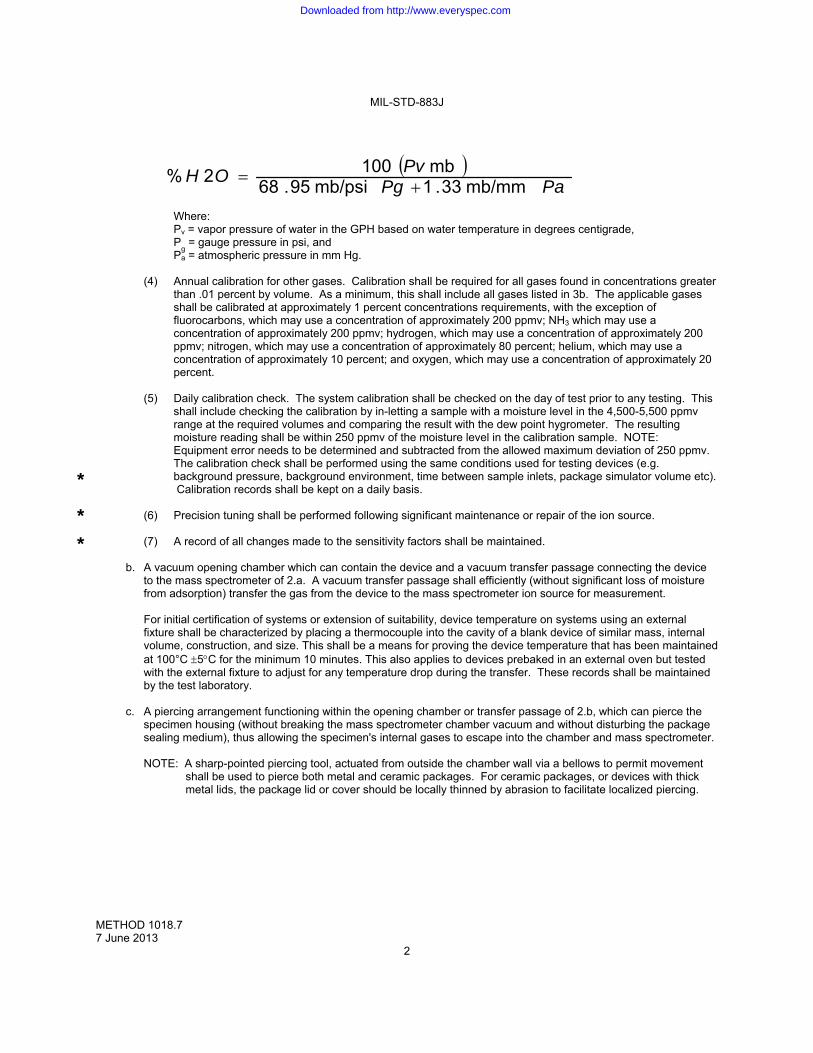
MIL-STD-883J
METHOD 1018.7 7 June 2013
2
Where: Pv = vapor pressure of water in the GPH based on water temperature in degrees centigrade, P
g = gauge pressure in psi, and
Pa = atmospheric pressure in mm Hg. (4) Annual calibration for other gases. Calibration shall be required for all gases found in concentrations greater
than .01 percent by volume. As a minimum, this shall include all gases listed in 3b. The applicable gases shall be calibrated at approximately 1 percent concentrations requirements, with the exception of fluorocarbons, which may use a concentration of approximately 200 ppmv; NH3 which may use a concentration of approximately 200 ppmv; hydrogen, which may use a concentration of approximately 200 ppmv; nitrogen, which may use a concentration of approximately 80 percent; helium, which may use a concentration of approximately 10 percent; and oxygen, which may use a concentration of approximately 20 percent.
(5) Daily calibration check. The system calibration shall be checked on the day of test prior to any testing. This
shall include checking the calibration by in-letting a sample with a moisture level in the 4,500-5,500 ppmv range at the required volumes and comparing the result with the dew point hygrometer. The resulting moisture reading shall be within 250 ppmv of the moisture level in the calibration sample. NOTE: Equipment error needs to be determined and subtracted from the allowed maximum deviation of 250 ppmv. The calibration check shall be performed using the same conditions used for testing devices (e.g. background pressure, background environment, time between sample inlets, package simulator volume etc). Calibration records shall be kept on a daily basis.
(6) Precision tuning shall be performed following significant maintenance or repair of the ion source.
(7) A record of all changes made to the sensitivity factors shall be maintained.
b. A vacuum opening chamber which can contain the device and a vacuum transfer passage connecting the device
to the mass spectrometer of 2.a. A vacuum transfer passage shall efficiently (without significant loss of moisture from adsorption) transfer the gas from the device to the mass spectrometer ion source for measurement.
For initial certification of systems or extension of suitability, device temperature on systems using an external
fixture shall be characterized by placing a thermocouple into the cavity of a blank device of similar mass, internal volume, construction, and size. This shall be a means for proving the device temperature that has been maintained at 100°C 5C for the minimum 10 minutes. This also applies to devices prebaked in an external oven but tested with the external fixture to adjust for any temperature drop during the transfer. These records shall be maintained by the test laboratory.
c. A piercing arrangement functioning within the opening chamber or transfer passage of 2.b, which can pierce the
specimen housing (without breaking the mass spectrometer chamber vacuum and without disturbing the package sealing medium), thus allowing the specimen's internal gases to escape into the chamber and mass spectrometer.
NOTE: A sharp-pointed piercing tool, actuated from outside the chamber wall via a bellows to permit movement
shall be used to pierce both metal and ceramic packages. For ceramic packages, or devices with thick metal lids, the package lid or cover should be locally thinned by abrasion to facilitate localized piercing.
PaPg
PvOHmb/mm33.1mb/psi95.68
mb1002%
*
*
*
Downloaded from http://www.everyspec.com
MIL-STD-883J
METHOD 1018.7 7 June 2013
3
d. A pressure sensing device located in the transfer passage to measure the pressure rise in the transfer passage
during the test. This pressure sensor is used to read a relative pressure change when the device is punctured. This relative pressure change indicates the relative quantity of gas in the device when comparing the test results of one device to another device. The significance of the reading is not intended to be absolute. Although the pressure gauge reading is reported, the pressure gauge is for indication only.
3. PROCEDURE. All devices shall be prebaked for 16 to 24 hours at 100°C ±5°C prior to test. Ovens shall have a means to indicate if a power interruption occurs during the prebaking period and for how long the temperature drops below 100°C 5C. Devices whose temperature drops below 100°C 5C for more than 1 hour shall undergo another prebake to begin a minimum of 12 hours later. A maximum 5 minute transfer time from prebake to hot insertion into apparatus shall be allowed. If 5 minutes is exceeded, device shall be returned to the prebake oven and prebake continued until device reaches 100°C 5C. The system shall be maintained at a stable temperature equal to or above the device temperature. The fixturing in the vacuum opening chamber shall position the specimen as required by the piercing arrangement of 2.c, and maintain the device at 100°C ±5°C for a minimum of 10 minutes prior to piercing. After device insertion, the device and chamber shall be pumped down and baked out at a temperature of 100°C ±5°C until the background pressure level will not prevent achieving the specified measurement accuracy and sensitivity. The background vacuum spectra shall be acquired and shall later be subtracted from the sample spectra. After pump down, the device case or lid shall be punctured and the following properties of the released gases shall be measured, using the mass spectrometer: a. The water-vapor content of the released gases, as a percent by unit volume or ppmv of the total gas content. b. The proportions (by volume) of the other following gases: N2, He, Mass 69 (fluorocarbons), O2, Ar, H2, CO2, CH4,
NH3, and other solvents, if available. Calculations shall be made and reported on all gases present. Data reduction shall be performed in a manner, which will preclude the cracking pattern interference from other gas specie in the calculations of moisture content. Data shall be corrected for any system dependent matrix effects such as the presence of hydrogen in the internal ambient.
c. The increase in chamber pressure as the gases are released by piercing the device package. A pressure change
of ±25 percent from expected for that package volume and pressurization may indicate that (1) the puncture was not fully accomplished, (2) the device package was not sealed hermetically, or (3) does not contain the normal internal pressure.
d. The test laboratory should provide comments describing the spectra of unknowns or gases that are present but not
in sufficient concentration to be identified or quantified with reasonable certainty.
e. If the test laboratory has reason to believe that the test results may be invalid due to reasons such as improper puncture of the device or equipment malfunction, the results shall be reported as “no test” with additional comments provided. The device may be replaced with another.
NOTE: The device shall be hermetic in accordance with test method 1014 of this standard, and free from any surface
contaminants which may interfere with accurate water vapor content measurement. The internal gas analysis laboratory is not required to test for hermeticity in accordance with test method 1014 of this standard. It is recommended that samples submitted for testing shall include information about the manufacturing process, including sealing pressure, sealing gas, free internal cavity volume, lid thickness at puncture site, lid material, and the location of the puncture site.
Downloaded from http://www.everyspec.com
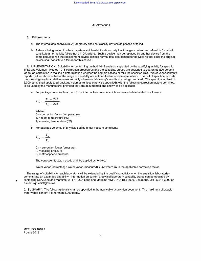
MIL-STD-883J
METHOD 1018.7 7 June 2013
4
3.1 Failure criteria. a. The Internal gas analysis (IGA) laboratory shall not classify devices as passed or failed. b. A device being tested in a batch system which exhibits abnormally low total gas content, as defined in 3.c, shall
constitute a hermeticity failure not an IGA failure. Such a device may be replaced by another device from the same population; if the replacement device exhibits normal total gas content for its type; neither it nor the original device shall constitute a failure for this cause.
4. IMPLEMENTATION. Suitability for performing method 1018 analysis is granted by the qualifying activity for specific limits and volumes. Method 1018 calibration procedures and the suitability survey are designed to guarantee ±20 percent lab-to-lab correlation in making a determination whether the sample passes or fails the specified limit. Water vapor contents reported either above or below the range of suitability are not certified as correlatable values. This out of specification data has meaning only in a relative sense and only when one laboratory's results are being compared. The specification limit of 5,000 ppmv shall apply to all package volumes (unless otherwise specified), with the following correction factors permitted, to be used by the manufacturer provided they are documented and shown to be applicable: a. For package volumes less than .01 cc internal free volume which are sealed while heated in a furnace:
273
273
s
rT T
TC
Where: CT = correction factor (temperature) Tr = room temperature (C) Ts = sealing temperature (C).
b. For package volumes of any size sealed under vacuum conditions:
a
sP P
PC
CP = correction factor (pressure) Ps = sealing pressure Pa = atmospheric pressure The correction factor, if used, shall be applied as follows: Water vapor (corrected) = water vapor (measured) x CX; where CX is the applicable correction factor.
The range of suitability for each laboratory will be extended by the qualifying activity when the analytical laboratories
demonstrate an expanded capability. Information on current analytical laboratory suitability status can be obtained by contacting DLA Land and Maritime, ATTN: DLA Land and Maritime-VQH, P.O. Box 3990, Columbus, OH 43218-3990 or e-mail: [email protected]. 5. SUMMARY. The following details shall be specified in the applicable acquisition document: The maximum allowable water vapor content if other than 5,000 ppmv.
*
Downloaded from http://www.everyspec.com
MIL-STD-883J
METHOD 1019.9 7 June 2013
1
METHOD 1019.9 IONIZING RADIATION (TOTAL DOSE) TEST PROCEDURE 1. PURPOSE. This test procedure defines the requirements for testing packaged semiconductor integrated circuits for ionizing radiation (total dose) effects from a cobalt-60 (60Co) gamma ray source. There are four (4) tests presented in this procedure: A standard room temperature irradiation test, an irradiation at elevated temperature/cryogenic temperature test, an accelerated annealing test, and an Enhanced Low Dose Rate Sensitivity (ELDRS) test. The accelerated annealing test estimates how dose rate ionizing radiation effects on devices is important for low dose-rate or certain other applications in which devices may exhibit significant time-dependent effects. The ELDRS test determines if devices with bipolar linear components exhibit sensitivity to enhanced radiation induced damage at low dose rates. This procedure addresses only steady state irradiations, and is not applicable to pulse type irradiations. These tests may produce severe degradation of the electrical properties of irradiated devices and thus should be considered destructive tests. 1.1 Definitions. Definitions of terms used in this procedure are given below:
a. Ionizing radiation effects. The changes in the electrical parameters of a device or integrated circuit resulting from radiation-induced charge. These are also referred to as total dose effects.
b. In-flux test. Electrical measurements made on devices during irradiation exposure. c. Internal dose-pattern. This is in reference to the state vector which specifies the logic condition of all elements
within a logic circuit during radiation exposure. d. Not in-flux test. Electrical measurements made on devices at any time other than during irradiation. e. Remote tests. Electrical measurements made on devices which are physically removed from the radiation
location. f. Time dependent effects. Significant degradation in electrical parameters caused by the growth or annealing or
both of radiation-induced trapped charge after irradiation. Similar effects also take place during irradiation. g. Accelerated annealing test. A procedure utilizing elevated temperature to accelerate time-dependent effects.
h. Enhanced Low Dose Rate Sensitivity (ELDRS). Used to refer to a part that shows enhanced radiation induced damage at dose rates below 50 rad(Si)/s.
i. Overtest. A factor that is applied to the specification dose to determine the test dose level that the samples must
pass to be acceptable at the specification level. An ovetest factor of 1.5 means that the parts must be tested at 1.5 times the specification dose.
j Parameter Delta Design Margin (PDDM). A design margin that is applied to the radiation induced change in an
electrical parameter. For a PDDM of 2 the change in a parameter at a specified dose from the pre-irradiation value is multiplied by two and added to the pre-irradiation value to see if the sample exceeds the post-irradiation parameter limit. For example, if the pre-irradiation value of Ib is 30 nA and the post-irradiation value at 20 krad(Si) is 70 nA (change in Ib is 40 nA), then for a PDDM of 2 the post-irradiation value would be 110 nA (30 nA + 2 X 40 nA). If the allowable post-irradiation limit is 100 nA the part would fail.
2. APPARATUS. The apparatus shall consist of the radiation source, electrical test instrumentation, test circuit board(s), cabling, interconnect board or switching system, an appropriate dosimetry measurement system, and an environmental chamber (if required for time-dependent effects measurements or elevated/cryogenic temperature irradiation). Adequate precautions shall be observed to obtain an electrical measurement system with sufficient insulation, ample shielding, satisfactory grounding, and suitable low noise characteristics. 2.1 Radiation source. The radiation source used in the test shall be the uniform field of a 60Co gamma ray source. Uniformity of the radiation field in the volume where devices are irradiated shall be within ±10 percent as measured by the dosimetry system, unless otherwise specified. The intensity of the gamma ray field of the 60Co source shall be known with an uncertainty of no more than ±5 percent. Field uniformity and intensity can be affected by changes in the location of the device with respect to the radiation source and the presence of radiation absorption and scattering materials.
*
*
*
*
Downloaded from http://www.everyspec.com
MIL-STD-883J
METHOD 1019.9 7 June 2013
2
2.2 Dosimetry system. An appropriate dosimetry system shall be provided which is capable of carrying out the measurements called for in 3.2. The following American Society for Testing and Materials (ASTM) standards and guidelines or other appropriate standards and guidelines shall be used: ASTM E 666 - Standard Method for Calculation of Absorbed Dose from Gamma or X Radiation. ASTM E 668 - Standard Practice for the Application of Thermoluminescence Dosimetry (TLD) Systems for Determining Absorbed Dose in Radiation-Hardness Testing of Electronic Devices. ASTM E 1249 - Minimizing Dosimetry Errors in Radiation Hardness Testing of Silicon Electronic Devices. ASTM E 1250 - Standard Method for Application of Ionization Chambers to Assess the Low Energy Gamma Component of Cobalt 60 Irradiators Used in Radiation Hardness Testing of Silicon Electronic Devices. ASTM F 1892 - Standard Guide for Ionizing Radiation (Total Dose) Effects Testing of Semiconductor Devices. ISO/ASTM 51275 Standard Practice for Use of a Radiochromic Film Dosimetry Systems. These industry standards address the conversion of absorbed dose from one material to another, and the proper use of various dosimetry systems. 1/ 2.3 Electrical test instruments. All instrumentation used for electrical measurements shall have the stability, accuracy, and resolution required for accurate measurement of the electrical parameters. Any instrumentation required to operate in a radiation environment shall be appropriately shielded. 2.4 Test circuit board(s). Devices to be irradiated shall either be mounted on or connected to circuit boards together with any associated circuitry necessary for device biasing during irradiation or for in-situ measurements. Unless otherwise specified, all device input terminals and any others which may affect the radiation response shall be electrically connected during irradiation, i.e., not left floating. The geometry and materials of the completed board shall allow uniform irradiation of the devices under test. Good design and construction practices shall be used to prevent oscillations, minimize leakage currents, prevent electrical damage, and obtain accurate measurements. Only sockets which are radiation resistant and do not exhibit significant leakages (relative to the devices under test) shall be used to mount devices and associated circuitry to the test board(s). All apparatus used repeatedly in radiation fields shall be checked periodically for physical or electrical degradation. Components which are placed on the test circuit board, other than devices under test, shall be insensitive to the accumulated radiation or they shall be shielded from the radiation. Test fixtures shall be made such that materials will not perturb the uniformity of the radiation field intensity at the devices under test. Leakage current shall be measured out of the radiation field. With no devices installed in the sockets, the test circuit board shall be connected to the test system such that all expected sources of noise and interference are operative. With the maximum specified bias for the test device applied, the leakage current between any two terminals shall not exceed ten percent of the lowest current limit value in the pre-irradiation device specification. Test circuit boards used to bias devices during accelerated annealing must be capable of withstanding the temperature requirements of the accelerated annealing test and shall be checked before and after testing for physical and electrical degradation. 2.5 Cabling. Cables connecting the test circuit boards in the radiation field to the test instrumentation shall be as short as possible. If long cables are necessary, line drivers may be required. The cables shall have low capacitance and low leakage to ground, and low leakage between wires. 2.6 Interconnect or switching system. This system shall be located external to the radiation environment location, and provides the interface between the test instrumentation and the devices under test. It is part of the entire test system and subject to the limitation specified in 2.4 for leakage between terminals. 2.7 The environmental chamber. The environmental chamber for time-dependent effects testing, if required, shall be capable of maintaining the selected accelerated annealing temperature within ±5°C. The environmental chamber for cryogenic temperature testing, if required, shall be capable of maintaining the selected irradiation temperature within ±5°C. 1/ Copies of these documents are available online at http://www.astm.org or from the American Society for Testing and Materials, P O Box C700, 100 Barr Harbor Drive, West Conshohocken, PA 19428-2959.
*
*
Downloaded from http://www.everyspec.com
MIL-STD-883J
METHOD 1019.9 7 June 2013
3
2.8 The irradiation temperature chamber. The irradiation temperature chamber, if required for elevated temperature irradiation should be capable of maintaining a circuit under test at 100 C + 5 C while it is being irradiated. The chamber should be capable of raising the temperature of the circuit under test from room temperature to the irradiation temperature within a reasonable time prior to irradiation and cooling the circuit under test from the irradiation temperature to room temperature in less than 20 minutes following irradiation. The irradiation bias shall be maintained during the heating and cooling. The method for raising, maintaining and lowering the temperature of the circuit under test may be by conduction through a heat sink using heating and cooling fluids, by convection using forced hot and cool air, or other means that will achieve the proper results. For cryogenic temperature irradiations, the chamber should be capable of maintaining the test device/unit at the required cryogenic temperature within + 5 C (e.g., liquid helium or liquid nitrogen) while it is being irradiated. The chamber should be capable of maintaining the cryogenic temperature of the test device/unit during post-irradiation electrical testing. 3. PROCEDURE. The test devices shall be irradiated and subjected to accelerated annealing testing (if required for time-dependent effects testing) as specified by a test plan. This plan shall specify the device description, irradiation conditions, device bias conditions, dosimetry system, operating conditions, measurement parameters and conditions, and accelerated annealing test conditions (if required). 3.1 Sample selection and handling. Only devices which have passed the electrical specifications as defined in the test plan shall be submitted to radiation testing. Unless otherwise specified, the test samples shall be randomly selected from the parent population and identically packaged. Each part shall be individually identifiable to enable pre- and post-irradiation comparison. For device types which are ESD-sensitive, proper handling techniques shall be used to prevent damage to the devices.
3.2 Burn-in. For some devices, there are differences in the total dose radiation response before and after burn-in. Unless it has been shown by prior characterization or by design that burn-in has negligible effect (parameters remain within postirradiation specified electrical limits) on the total dose radiation response, then one of the following must be done:
3.2.1 The manufacturer shall subject the radiation samples to the specified burn-in conditions prior to conducting total dose radiation testing or
3.2.2 The manufacturer shall develop a correction factor, (which is acceptable to the parties to the test) taking into account the changes in total dose response resulting from subjecting product to burn-in. The correction factor shall then be used to accept product for total dose response without subjecting the test samples to burn-in.
3.3 Dosimetry measurements. The radiation field intensity at the location of the device under test shall be determined prior to testing by dosimetry or by source decay correction calculations, as appropriate, to assure conformance to test level and uniformity requirements. The dose to the device under test shall be determined one of two ways: (1) by measurement during the irradiation with an appropriate dosimeter, or (2) by correcting a previous dosimetry value for the decay of the 60Co source intensity in the intervening time. Appropriate correction shall be made to convert from the measured or calculated dose in the dosimeter material to the dose in the device under test.
3.4 Lead/Aluminum (Pb/Al) container. Test specimens shall be enclosed in a Pb/Al container to minimize dose enhancement effects caused by low-energy, scattered radiation. A minimum of 1.5 mm Pb, surrounding an inner shield of at least 0.7 mm Al, is required. This Pb/Al container produces an approximate charged particle equilibrium for Si and for TLDs such as CaF2. The radiation field intensity shall be measured inside the Pb/Al container (1) initially, (2) when the source is changed, or (3) when the orientation or configuration of the source, container, or test-fixture is changed. This measurement shall be performed by placing a dosimeter (e.g., a TLD) in the device-irradiation container at the approximate test-device position. If it can be demonstrated that low energy scattered radiation is small enough that it will not cause dosimetry errors due to dose enhancement, the Pb/Al container may be omitted.
3.5 Radiation level(s). The test devices shall be irradiated to the dose level(s) specified in the test plan within ±10 percent. If multiple irradiations are required for a set of test devices, then the post-irradiation electrical parameter measurements shall be performed after each irradiation.
3.6 Radiation dose rate. The radiation dose rate for bipolar and BiCMOS linear or mixed-signal parts used in applications where the maximum dose rate is below 50 rad(Si)/s shall be determined as described in paragraph 3.13 below. Parts used in low dose rate applications, unless they have been demonstrated to not exhibit an ELDRS response shall use Condition C, Condition D, or Condition E. NOTE: Devices that contain both MOS and bipolar devices may require qualification to multiple subconditions to ensure that both
ELDRS and traditional MOS effects are evaluated.
*
Downloaded from http://www.everyspec.com
MIL-STD-883J
METHOD 1019.9 7 June 2013
4
3.6.1 Condition A. For condition A (standard condition) the dose rate shall be between 50 and 300 rad(Si)/s [0.5 and 3
Gy(Si)/s] 60Co 2/ The dose rates may be different for each radiation dose level in a series; however, the dose rate shall not vary by more than ±10 percent during each irradiation.
3.6.2 Condition B. For condition B, for MOS devices only, if the maximum dose rate is < 50 rad(Si)/s in the intended application, the parties to the test may agree to perform the test at a dose rate ≥ the maximum dose rate of the intended application. Unless the exclusions in 3.12.1b are met, the accelerated annealing test of 3.12.2 shall be performed.
3.6.3 Condition C. For condition C, (as an alternative) the test may be performed at the dose rate agreed to by the parties to the test. Where the final user is not known, the test conditions and results shall be made available in the test report with each purchase order.
3.6.4 Condition D. For condition D, for bipolar or BiCMOS linear or mixed-signal devices only, the parts shall be irradiated at mrad(Si)/s.
3.6.5 Condition E. For condition E, for bipolar or BiCMOS linear or mixed-signal devices only, the parts shall be irradiated with the accelerated test conditions determined by characterization testing as discussed in paragraph 3.13.2. The accelerated test may include irradiation at an elevated temperature.
3.7 Temperature requirements. The following requirements shall apply for room temperature and elevated temperature irradiation.
3.7.1 Room temperature irradiation. Since radiation effects are temperature dependent, devices under test shall be
irradiated in an ambient temperature of 24°C ±6°C as measured at a point in the test chamber in close proximity to the test fixture. The electrical measurements shall be performed in an ambient temperature of 24°C ± 6°C. If devices are transported to and from a remote electrical measurement site, the temperature of the test devices shall not be allowed to increase by more than 10°C from the irradiation environment. If any other temperature range is required, it shall be specified.
Caution: Annealing at ambient temperatures above the irradiation temperature may be significant, especially for the
extended times allowed for the time between irradiations at low dose rate (Condition D). It is important to assure that the temperature of the parts is maintained within the above stated requirements to minimize annealing.
3.7.2 Elevated temperature irradiation. For bipolar or BiCMOS linear or mixed-signal devices irradiated using Condition
E elevated temperature irradiation test, devices under test shall be irradiated in an ambient temperature determined by characterization testing (see paragraph 3.13.2) as measured at a point in the test chamber in close proximity to the test fixture (see paragraph 2.8 for details on raising and lowering the irradiation temperature).
3.7.3 Cryogenic temperature irradiation. For test devices/units operated in cryogenic temperature applications, the
devices/units shall be irradiated at cryogenic temperature (see paragraph 2.8) and maintained at cryogenic temperature for post exposure characterization testing (see paragraph 3.10). The test device/units shall remain at cryogenic temperature throughout all irradiations and characterization testing until the final total dose exposure and characterization have been completed.
3.8 Electrical performance measurements. The electrical parameters to be measured and functional tests to be
performed shall be specified in the test plan. As a check on the validity of the measurement system and pre- and post-irradiation data, at least one control sample shall be measured using the operating conditions provided in the governing device specifications. For automatic test equipment, there is no restriction on the test sequence provided that the rise in the device junction temperature is minimized. For manual measurements, the sequence of parameter measurements shall be chosen to allow the shortest possible measurement period. When a series of measurements is made, the tests shall be arranged so that the lowest power dissipation in the device occurs in the earliest measurements and the power dissipation increases with subsequent measurements in the sequence. The pre- and post-irradiation electrical measurements shall be done on the same measurement system and the same sequence of measurements shall be maintained for each series of electrical measurements of devices in a test sample. Pulse-type measurements of electrical parameters should be used as appropriate to minimize heating and subsequent annealing effects. Devices which will be subjected to the accelerated annealing testing (see 3.12) may be given a preirradiation burn-in to eliminate burn-in related failures. 2/ The SI unit for the quantity absorbed dose is the gray, symbol Gy. 100 rad = 1 Gy.
*
*
Downloaded from http://www.everyspec.com
MIL-STD-883J
METHOD 1019.9 7 June 2013
5
3.9 Test conditions. The use of in-flux or not in-flux testing shall be specified in the test plan. (This may depend on the
intended application for which the data are being obtained.) The use of in-flux testing may help to avoid variations introduced by post-irradiation time dependent effects. However, errors may be incurred for the situation where a device is irradiated in-flux with static bias, but where the electrical testing conditions require the use of dynamic bias for a significant fraction of the total irradiation period. Not-in-flux testing generally allows for more comprehensive electrical testing, but can be misleading if significant post-irradiation time dependent effects occur.
3.9.1 In-flux testing. Each test device shall be checked for operation within specifications prior to being irradiated. After the entire system is in place for the in-flux radiation test, it shall be checked for proper interconnections, leakage (see 2.4), and noise level. To assure the proper operation and stability of the test setup, a control device with known parameter values shall be measured at all operational conditions called for in the test plan. This measurement shall be done either before the insertion of test devices or upon completion of the irradiation after removal of the test devices or both.
3.9.2 Remote testing. Unless otherwise specified, the bias shall be removed and the device leads placed in conductive
foam (or similarly shorted) during transfer from the irradiation source to a remote tester and back again for further irradiation. This minimizes post-irradiation time dependent effects.
3.9.3 Bias and loading conditions. Bias and loading conditions for test devices during irradiation or accelerated
annealing shall be within ±10 percent of those specified by the test plan. The bias, loading and internal dose-pattern applied to the test devices shall be selected to produce the greatest radiation induced damage or the worst-case damage for the intended application, if known. The bias, loading and internal dose-pattern conditions shall remain constant throughout a step-wise Total Ionizing Dose (TID) exposure and anneal. If any of the bias, loading or internal dose-pattern conditions are not at the worst-case condition, then a justification for the conditions used shall be provided in the test plan and test report. While maximum voltage is often worst case some bipolar linear device parameters (e.g. input bias current or maximum output load current) exhibit more degradation with 0 V bias. The specified bias shall be maintained on each device in accordance with the test plan. Bias shall be checked immediately before and after irradiation. Care shall be taken in selecting the loading such that the rise in the junction temperature is minimized.
3.10 Post-irradiation procedure. Unless otherwise specified, the following time intervals shall be observed:
a. The time from the end of an irradiation to the start of electrical measurements shall be a maximum of 1 hour for Condition A. For Conditions B, C, D and E, the time from the end of an irradiation to the start of electrical measurements may be equal to 10% of the incremental irradiation time up to (but not exceeding) 72 hours if this time is greater than 1 hour, otherwise it shall be a maximum of 1 hour. As an option for remote electrical testing, for Conditions A, B, C, D and E, parts may be packed in dry ice until the start of electrical testing, but only if packed within 15 minutes after the completion of irradiation. While in dry ice, the part leads shall be shorted, the parts shall be verifiably maintained at a maximum temperature of -60 C, and the time from completion of irradiation until the start of electrical testing may not exceed 72 hours. The electrical testing shall be conducted after the parts have been restored to room temperature but within 30 minutes after the parts are removed from the dry ice. Electrical testing shall be as specified in paragraph 3.7.1. The times at room temperature and the times and temperature for the dry ice procedure may be different if demonstrated by a characterization test as described in paragraph 3.10.c below.
b. The time to perform the electrical measurements and to return the device for a subsequent irradiation, if any, shall
be within two hours of the end of the prior irradiation for Condition A. For conditions B, C, D and E, the time to perform the electrical measurements and to return the device for a subsequent irradiation, if any, may be equal to 20% of the incremental irradiation time up to (but not exceeding) 120 hours if this time is greater than 2 hours, otherwise it shall be a maximum of 2 hours. As an option for continued additional irradiation when parts are electrically tested at a remote location, for Conditions A, B, C, D and E parts may be packed in dry ice until the start of irradiation, but only if packed within 15 minutes after the completion of electrical testing. While in the dry ice, the part leads shall be shorted, the parts shall be verifiably maintained at a maximum temperature of -60 C, and the time from completion of electrical testing until the start of irradiation may not exceed 72 hours. The radiation exposure shall begin after the parts have been restored to room temperature but within 30 minutes after the parts are removed from the dry ice. The times at room temperature and the times and temperature for the dry ice procedure may be different if demonstrated by a characterization test as described in paragraph 3.10.c below.
*
*
Downloaded from http://www.everyspec.com
MIL-STD-883J
METHOD 1019.9 7 June 2013
6
c. If the dry ice test method is used, characterization test shall be performed on annealing at the particular technology
node of study to demonstrate that the annealing will be less than 10% for all critical parameters compared to room temperature data taken within 1 hour after irradiation. Other times and temperatures than those listed in paragraphs 3.10.a and 3.10.b may be considered as part of the characterization test. However, the time for electrical measurements following irradiation shall not exceed 72 hours and the time between successive irradiations shall not exceed 120 hours. For example, if the manufacturer’s cold temperature specification limit is higher than -60 C this higher temperature may be allowed. For another example, if the parts show very little annealing at room temperature following Condition A irradiation, the one hour and two hour limits may want to be increased. For any exceptions to the times and temperatures in 3.10.a and 3.10.b it must be demonstrated that the annealing under these different conditions is within 10% for all critical parameters compared to room temperature data taken within 1 hour after irradiation, or the appropriate time limit for the irradiation test condition, if greater than 1 hour. The characterization test results shall be included with the test report as specified in paragraph 3.14.
To minimize time dependent effects, these intervals shall be as short as possible. The sequence of parameter measurements shall be maintained constant throughout the tests series.
3.11 Extended room temperature anneal test. The tests of 3.1 through 3.10 are known to be overly conservative for
some devices in a very low dose rate environment (e.g. dose rates characteristic of space missions). The extended room temperature anneal test provides an estimate of the performance of a device in a very low dose rate environment even though the testing is performed at a relatively high dose rate (e.g. 50-300 rad(Si)/s). The procedure involves irradiating the device per steps 3.1 through 3.10 and post-irradiation subjecting the device under test to a room temperature anneal for an appropriate period of time (see 3.11.2c) to allow leakage-related parameters that may have exceeded their pre-irradiation specification to return to within specification. The procedure is known to lead to a higher rate of device acceptance in cases:
a. where device failure when subjected to the tests in 3.1 through 3.10 has been caused by the buildup of trapped
positive charge in relatively soft oxides, and
b. where this trapped positive charge anneals at a relatively high rate. 3.11.1 Need to perform an extended room temperature anneal test. The following criteria shall be used to determine
whether an extended room temperature anneal test is appropriate:
a. The procedure is appropriate for either MOS or bipolar technology devices.
b. The procedure is appropriate where only parametric failures (as opposed to functional failure) occurs. The parties to the test shall take appropriate steps to determine that the device under test is subject to only parametric failure over the total ionizing dose testing range.
c. The procedure is appropriate where the natural annealing response of the device under test will serve to correct the
out-of-specification of any parametric response. Further, the procedure is known to lead to a higher rate of device acceptance in cases where the expected application irradiation dose rate is sufficiently low that ambient temperature annealing of the radiation induced trapped positive charge can lead to a significant improvement of device behavior. Cases where the expected application dose rate is lower than the test dose rate and lower than 0.1 rad(Si)/s should be considered candidates for the application of this procedure. The parties to the test shall take appropriate steps to determine that the technology under test can provide the required annealing response over the total ionizing dose testing range.
Downloaded from http://www.everyspec.com
MIL-STD-883J
METHOD 1019.9 7 June 2013
7
3.11.2 Extended room temperature anneal test procedure. If the device fails the irradiation and testing specified in 3.1
through 3.10, an additional room temperature annealing test may be performed as follows:
a. Following the irradiation and testing of 3.1 through 3.10, subject the device under test to a room temperature anneal under worst-case static bias conditions. For information on worst case bias see 3.9.3,
b. The test will be carried out in such a fashion that the case of the device under test will have a temperature within
the range 24°C ± 6°C.
c. Where possible, the room temperature anneal should continue for a length of time great enough to allow device parameters that have exceeded their pre-irradiation specification to return to within specification or post-irradiation- parametric limit (PIPL) as established by the manufacturer. However, the time of the room temperature anneal shall not exceed tmax, where
Dspec tmax = Rmax
Dspec is the total ionizing dose specification for the part and Rmax is the maximum dose rate for the intended use.
d. Test the device under test for electrical performance as specified in 3.7 and 3.8. If the device under test passes electrical performance tests following the extended room temperature anneal, this shall be considered acceptable performance for a very low dose rate environment in spite of having previously failed the post-irradiation and electrical tests of 3.1 through 3.10.
3.12 MOS accelerated annealing test. The accelerated annealing test provides an estimate of worst-case degradation of
MOS microcircuits in low dose rate environments. The procedure involves heating the device following irradiation at specified temperature, time and bias conditions. An accelerated annealing test (see 3.12.2) shall be performed for cases where Time Dependent Effects (TDE) can cause a device to degrade significantly or fail. Only standard testing shall be performed as specified in 3.1 through 3.10 for cases where TDE are known not to cause significant device degradation or failure (see 3.12.1) or where they do not need to be considered, as specified in 3.12.1.
3.12.1 Need to perform accelerated annealing test. The parties to the test shall take appropriate steps to determine whether accelerated annealing testing is required. The following criteria shall be used:
a. The tests called out in 3.12.2 shall be performed for any device or circuit type that contains MOS circuit elements (i.e., transistors or capacitors).
b. TDE tests may be omitted if:
1. devices are known not to contain MOS elements by design, or 2. the ionizing dose in the application, if known, is below 5 krad(Si), or 3. the lifetime of the device from the onset of the irradiation in the intended application, if known, is short
compared with TDE times, or 4. the test is carried out at the dose rate of the intended application, or 5. the device type or IC technology has been demonstrated via characterization testing not to exhibit TDE
changes in device parameters greater than experimental error (or greater than an otherwise specified upper limit) and the variables that affect TDE response are demonstrated to be under control for the specific vendor processes.
At a minimum, the characterization testing in (5) shall include an assessment of TDE on propagation delay,
output drive, and minimum operating voltage parameters. Continuing process control of variables affecting TDE may be demonstrated through lot sample tests of the radiation hardness of MOS test structures.
c. This document provides no guidance on the need to perform accelerated annealing tests on technologies that do
not include MOS circuit elements.
Downloaded from http://www.everyspec.com
MIL-STD-883J
METHOD 1019.9 7 June 2013
8
3.12.2 Accelerated annealing test procedure. If the device passes the tests in 3.1 through 3.10 or if it passes 3.11 (if that procedure is used) to the total ionizing dose level specified in the test plan or device specification or drawing and the exclusions of 3.12.1 do not apply, the accelerated annealing test shall be conducted as follows:
a. Overtest.
1. Irradiate each test device to an additional 0.5-times the specified dose using the standard test conditions (3.1 through 3.10). Note that no electrical testing is required at this time.
2. The additional 0.5-times irradiation in 3.12.2.a.1may be omitted if it has been demonstrated via
characterization testing that:
a. none of the device propagation delay, output drive, and minimum operating voltage parameters recover toward their pre-irradiation value greater than experimental accelerated annealing test of 3.12.2.b, and
b. the irradiation biases chosen for irradiation and accelerated annealing tests are worst-case for the
response of these parameters during accelerated annealing. The characterization testing to establish worst-case irradiation and annealing biases shall be performed at the specified level. The testing shall at a minimum include separate exposures under static and dynamic irradiation bias, each followed by worst-case static bias during accelerated annealing according to 3.12.2.b.
b. Accelerated annealing. Heat each device under worst-case static bias conditions in an environmental chamber according to one of the following conditions:
1. At 100°C ±5°C for 168 ±12 hours, or
2. At an alternate temperature and time that has been demonstrated via characterization testing to cause equal
or greater change in the parameter(s) of interest, e.g., propagation delay, output drive, and minimum operating voltage, in each test device as that caused by 3.12.2.b.1, or
3. At an alternate temperature and time which will cause trapped hole annealing of >60% and interface state
annealing of <10% as determined via characterization testing of NMOS test transistors from the same process. It shall be demonstrated that the radiation response of test transistors represent that of the device under test.
c. Electrical testing. Following the accelerated annealing, the electrical test measurements shall be performed as
specified in 3.8 and 3.9.
Downloaded from http://www.everyspec.com
MIL-STD-883J
METHOD 1019.9 7 June 2013
9
3.13 Test procedure for Bipolar and BiCMOS linear or mixed signal devices with intended application dose rates less
than 50 rad(Si)/s. Many bipolar linear parts exhibit ELDRS, which cannot be simulated with a room temperature 50-300 rad(Si)/s irradiation plus elevated temperature anneal, such as that used for MOS parts (see ASTM-F-1892 for more technical details). Parts that exhibit ELDRS shall be tested either at the intended application dose rate, at a prescribed low dose rate to an overtest radiation level, or with an accelerated test such as an elevated temperature irradiation test that includes a parameter delta design margin (see characterization test for ELDRS parts, paragraph 3.13.2). For part types that have not been characterized for ELDRS a characterization test shall be performed to determine if the part types are ELDRS susceptible. Need to perform ELDRS testing.
a. The ELDRS tests described in 3.13 may be omitted if:
1. devices are known not to contain bipolar transistors by design, or 2. devices are known not to contain any linear circuit functions by design. 3. the device type and IC technology have been demonstrated via characterization testing not to exhibit
ELDRS (paragraph 3.13.1) in device parameters greater than experimental error and the variables that affect ELDRS response are demonstrated to be under control for the specific vendor processes.
3.13.1 Characterization test to determine if a part exhibits ELDRS. If a part cannot be eliminated by the criteria in
paragraph 3.13 and has not been characterized for ELDRS then the part shall be subjected to a characterization test to determine if it exhibits ELDRS. This test shall be performed at two dose rates. If the part meets the criteria for ELDRS then an additional characterization test may be performed to establish the irradiation conditions for production or lot acceptance tests.
3.13.1.1 Characterization test to determine if a part exhibits ELDRS. Select a minimum random sample of 21 devices from a population representative of recent production runs. Smaller sample sizes may be used if agreed upon between the parties to the test. All of the selected devices shall have undergone appropriate elevated temperature reliability screens, e.g. burn-in and high temperature storage life. Divide the samples into four groups of 5 each and use the remaining part for a control. Perform pre-irradiation electrical characterization on all parts assuring that they meet the Group A electrical tests. Irradiate 5 samples under a 0 volt bias and another 5 under the irradiation bias given in the acquisition specification at 50-300 rad(Si)/s and room temperature. Irradiate 5 samples under a 0 volt bias and another 5 under irradiation bias given in the acquisition specification at < 10 mrad(Si)/s and room temperature. Irradiate all samples to the same dose levels, including 0.5 and 1.0 times the anticipated specification dose, and repeat the electrical characterization on each part at each dose level. Post irradiation electrical measurements shall be performed per paragraph 3.10 where the low dose rate test is considered Condition D. Calculate the radiation induced change in each electrical parameter (para) for each sample at each radiation level. Calculate the ratio of the median para at low dose rate to the median para at high dose rate for each irradiation bias group at each total dose level. If this ratio exceeds 1.5 for any of the most sensitive parameters then the part is considered to be ELDRS susceptible. This test does not apply to parameters which exhibit changes that are within experimental error or whose values are below the pre-irradiation electrical specification limits at low dose rate at the specification dose.
3.13.2 Characterization of ELDRS parts to determine the irradiation conditions for production or lot acceptance testing. If the part type is known to exhibit ELDRS or has been shown to exhibit ELDRS by the characterization tests in paragraphs 3.13.1.1 then the production or lot acceptance testing may be performed using the default low dose rate test at < 10 mrad(Si)/s (Condition D) or an accelerated test (Condition E). For the accelerated test a detailed characterization shall be performed to establish the test parameters for the test The accelerated test approach may include one of the following methods: 1) a room temperature low dose rate irradiation at a dose rate > 10 mrad(Si)/s, 2) an elevated temperature irradiation, 3) combinations of high dose rate tests and elevated temperature anneals, 4) switched dose rates, or 5) some other form of accelerated testing (for guidance on characterization of ELDRS parts see ASTM F1892 Appendix X2). The characterization testing of the ELDRS parts must demonstrate that the irradiation test procedure for production or lot acceptance testing will bound the low dose rate response for all critical electrical parameters at a dose rate of < 10 mrad(Si)/s using a combination of overtest and/or parameter delta design margins. Hence the characterization testing shall include irradiation at < 10 mrad(Si)/s, to the specification dose, as a baseline for comparison.
Downloaded from http://www.everyspec.com
MIL-STD-883J
METHOD 1019.9 7 June 2013
10
3.13.3 Low dose rate or elevated temperature irradiation test for bipolar or BiCMOS linear or mixed-signal devices. All devices that do not meet the exception of 3.13.a shall be tested using one of the following test conditions:
a. Test at the agreed to dose rate. Irradiate each test device at the dose rate described in 3.6.3 Condition C using
the standard test conditions (3.1 through 3.10). b. Test at a prescribed low dose rate. Irradiate each test device at the dose rate described in 3.6.4 Condition D using
the standard test conditions (3.1 through 3.10) with the following additional requirements: an overtest factor of 1.5 shall be applied to the radiation level, i.e. the part must pass at a radiation level of 1.5 times the specification dose to be acceptable..
c. Test using an accelerated test method. Irradiate each test device with the accelerated test condition described in
3.6.5 Condition E using the standard test conditions (3.1 through 3.10) with the following additional requirements: a parameter delta design margin and/or overtest factor shall be applied as established through characterization testing described in paragraph 3.13.2.
3.14 Test report. As a minimum, the report shall include the device type number, serial number, the manufacturer,
package type, controlling specification, date code, and any other identifying numbers given by the manufacturer. The bias circuit, parameter measurement circuits, the layout of the test apparatus with details of distances and materials used, and electrical noise and current leakage of the electrical measurement system for in-flux testing shall be reported using drawings or diagrams as appropriate. Each data sheet shall include the test date, the radiation source used, the bias conditions during irradiation, the ambient temperature around the devices during irradiation and electrical testing, the duration of each irradiation, the time between irradiation and the start of the electrical measurements, the duration of the electrical measurements and the time to the next irradiation when step irradiations are used, the irradiation dose rate, electrical test conditions, dosimetry system and procedures and the radiation test levels. The pre- and post-irradiation data shall be recorded for each part and retained with the parent population data in accordance with the requirements of MIL-PRF-38535 or MIL-PRF-38534. Any anomalous incidents during the test shall be fully documented and reported. The accelerated annealing procedure, if used, shall be described. Any other radiation test procedures or test data required for the delivery shall be specified in the device specification, drawing or purchase order.
Downloaded from http://www.everyspec.com
MIL-STD-883J
METHOD 1019.9 7 June 2013
11
4. SUMMARY. The following details shall be specified in the applicable acquisition document as required:
a. Device-type number(s), quantity, and governing specifications (see 3.1). b. Radiation dosimetry requirements (see 3.3). c. Radiation test levels including dose and dose rate (see 3.5 and 3.6). d. Irradiation, electrical test and transport temperatures if other than as specified in 3.7. e. Test methodology used if not maintaining Cryogenic Temperature as specified in 3.7. f. Electrical parameters to be measured and device operating conditions during measurement (see 3.8). g. Test conditions, i.e., in-flux or not-in-flux type tests (see 3.9). h. Bias, loading and internal dose-pattern conditions for devices during irradiation (see 3.9.3). i. Time intervals of the post-irradiation measurements (see 3.10). j. Requirement for extended room temperature anneal test, if required (see 3.11). k. Requirement for accelerated annealing test, if required (see 3.12). l. Requirement for test for ELDRS, if required (see 3.13). m. Requirement for ELDRS testing, if required (see 3.13.3). n. Documentation required to be delivered with devices (see 3.14).
*
*
Downloaded from http://www.everyspec.com
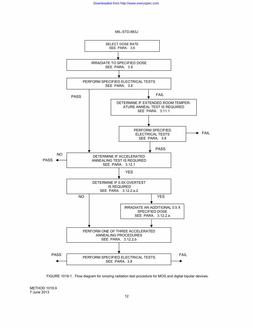
MIL-STD-883J
METHOD 1019.9 7 June 2013
12
FIGURE 1019-1. Flow diagram for ionizing radiation test procedure for MOS and digital bipolar devices.
NO YES
SELECT DOSE RATE SEE PARA. 3.6
IRRADIATE TO SPECIFIED DOSE SEE PARA. 3.9
PERFORM SPECIFIED ELECTRICAL TESTS SEE PARA. 3.8
DETERMINE IF EXTENDED ROOM TEMPER- ATURE ANNEAL TEST IS REQUIRED
SEE PARA. 3.11.1
PERFORM SPECIFIED ELECTRICAL TESTS
SEE PARA. 3.8
DETERMINE IF ACCELERATED ANNEALING TEST IS REQUIRED
SEE PARA. 3.12.1
DETERMINE IF 0.5X OVERTEST IS REQUIRED
SEE PARA. 3.12.2.a.2
IRRADIATE AN ADDITIONAL 0.5 X SPECIFIED DOSE
SEE PARA. 3.12.2.a
PERFORM ONE OF THREE ACCELERATED ANNEALING PROCEDURES
SEE PARA. 3.12.2.b
PERFORM SPECIFIED ELECTRICAL TESTS SEE PARA. 3.8
PASS FAIL
FAIL
PASS
PASS
NO
YES
PASS FAIL
Downloaded from http://www.everyspec.com
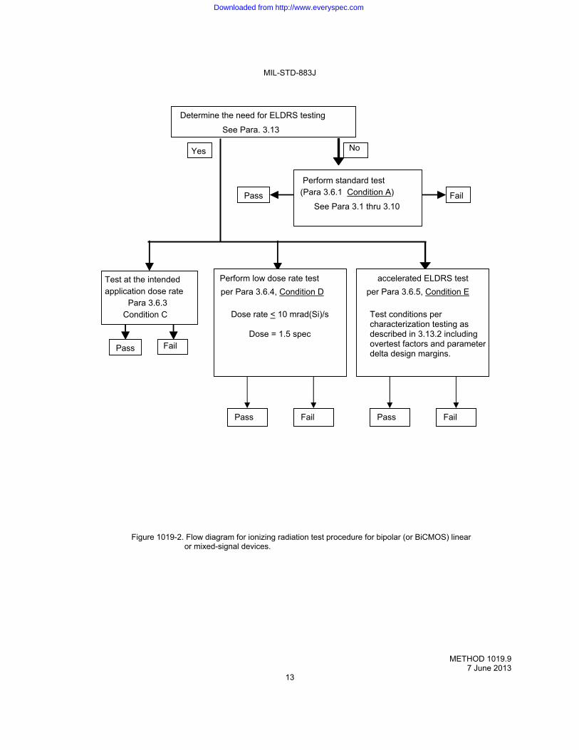
MIL-STD-883J
METHOD 1019.9 7 June 2013
13
Figure 1019-2. Flow diagram for ionizing radiation test procedure for bipolar (or BiCMOS) linear or mixed-signal devices.
Determine the need for ELDRS testing
See Para. 3.13
No Yes
Perform standard test (Para 3.6.1 Condition A)
See Para 3.1 thru 3.10 Pass Fail
Perform low dose rate test
per Para 3.6.4, Condition D
Dose rate < 10 mrad(Si)/s
Dose = 1.5 spec
accelerated ELDRS test
per Para 3.6.5, Condition E
Test conditions per characterization testing as described in 3.13.2 including overtest factors and parameter delta design margins.
Test at the intended application dose rate
Para 3.6.3 Condition C
Pass Fail
Pass Pass Fail Fail
Downloaded from http://www.everyspec.com
MIL-STD-883J
METHOD 1019.9 7 June 2013
14
This page intentionally left blank
Downloaded from http://www.everyspec.com
MIL-STD-883J
METHOD 1020.1 15 November 1991
1
METHOD 1020.1 DOSE RATE INDUCED LATCHUP TEST PROCEDURE 1. PURPOSE. This test procedure defines the detailed requirements for performing latchup testing of microcircuits to identify susceptibility to dose rate induced latchup. 1.1 Definitions. Definitions of terms used in this procedure are provided below: a. Dose rate induced latchup. Dose rate induced latchup is regenerative device action in which a parasitic region
(e.g., a four layer p-n-p-n or n-p-n-p path) is turned on by a photocurrent generated by a pulse of ionizing radiation, and remains on for an indefinite period of time after the photocurrent subsides. The device will remain latched as long as the power supply delivers voltage greater than the holding voltage and current greater than the holding current. Latchup disrupts normal circuit operation in some portion of the circuit, and may also cause catastrophic failure due to local heating of semiconductor regions, metallization or bond wires.
b. Latchup windows. A latchup window is the phenomenon in which a device exhibits latchup in a specific range of
dose rates. Above and below this range, the device does not latchup. A device may exhibit more than one latchup window. This phenomenon has been observed for some CMOS logic devices, oxide sidewall logic and LSI memories, and may occur in other devices.
c. Combinational logic. Combinational (determined) logic devices are those whose output is solely determined by
the logic signals at its inputs (except for switching delays). Combinational logic circuits contain no internal storage elements, and include multiplexers, decoders, and gates.
d. Sequential logic. Sequential (nondetermined) devices are those in which the output state at any given time
depends on the sequence and time relationship of logic signals that were previously applied to its inputs. Sequential logic circuits contain internal storage elements. Examples of sequential logic devices are shift registers, memories, counters, and flip-flops.
e. Recovery period. The recovery period is the time interval in which the device supply current recovers from the
radiation pulse. f. Holding voltage and holding current: The voltage and current above which latchup is sustained. 1.2 Test plan. Prior to latchup testing, a latchup test plan shall be prepared which describes the radiation source, the dosimetry techniques, test equipment and conditions to be used. A detailed procedure for each device type to be tested shall be prepared, either as part of the test plan or in separate test procedure documents. The procedure shall include bias conditions, test sequence, and schematics of the test setup. The test plan shall be approved by the acquiring activity, and as a minimum, the items listed below shall be provided in the test plan or test procedure: a. Device types, including package types, and quantities to be tested. b. Traceability requirements, such as requirements for serialization, wafer or lot traceability, etc. c. Requirements for data reporting and submission. d. Temperature for test (see 2.3.6). e. Block diagram or schematic representation of test set up. f. Electrical parameters to be monitored and device operating conditions, including bias conditions and functional
test requirements before, during, and after the radiation pulse. g. Group A electrical test requirements for pre- and post-latchup testing, to include test limits and failure criteria.
Downloaded from http://www.everyspec.com
MIL-STD-883J
METHOD 1020.1 15 November 1991
2
h. Radiation pulse width(s), radiation dose(s) per pulse and dose rate range(s). i. Total dose limit for each device type. j. Failure criteria. In addition to those items listed above, the test plan or procedure for production tests shall include the following: k. Method(s) to detect latchup, e.g., monitoring of the supply current, functional testing (to include test vector set,
etc.). l. Recovery period and when to begin post-irradiation in-situ tests. The recovery period for SSI devices is typically
50 to 300 s; however, other device types may require a longer recovery period, or there may be special program requirements which call for earlier recovery.
m. Functional test requirements. The functional tests shall demonstrate that the device responds properly to input
commands and that the device is operating properly. Note that high speed functional tests may be incompatible with the long leads and unavoidable capacitance associated with most latchup test systems.
n. Exposure states or operating conditions. For digital devices, a specific state and its complement are usually used.
However, for more complex devices, more than two exposure states may be required, and the specific states shall be as determined by the characterization testing (and analysis, if required) and specified in the test plan or procedure.
o. Bias and load conditions. Unless otherwise specified, the maximum rated operating supply voltage shall be used. p. Outputs to be monitored. q. The minimum dc current that must be available from the power supply, or the value of series current limiting
resistor that has been approved by the acquiring activity. (Note that any current limiting resistor shall be less than or equal to that in the system application and shall be approved by the acquiring activity prior to latchup testing.)
2. APPARATUS. The apparatus shall consist of the radiation source, the dosimetry system, and the latchup test system which includes the device interface fixture, the test circuit, cabling, timing, and temperature control systems. Precautions shall be observed to obtain adequate electrical grounding to ensure low noise.
2.1 Radiation source. Either of two radiation sources shall be used for latchup testing: 1) a flash x-ray machine (FXR), or 2) an electron linear accelerator (LINAC). The FXR shall be used in the x-ray mode and the LINAC in the electron (e-beam) mode. The FXR peak (endpoint) energy shall be 2 MeV or greater, and the LINAC beam energy shall be 10 MeV or greater. The pulse width shall be from 20 to 100 ns, or as specified in the acquisition document, and the uniformity of the radiation field in the device irradiation volume shall be ±15 percent as measured by the dosimetry system. The dose per radiation exposure shall be as specified in the test plan or procedure. (See 3.5.1 for production test requirements.)
2.2 Dosimetry system. A dosimetry system shall be used which provides a measurement accuracy within ±15 percent. A calibrated PIN diode may be used to obtain both the shape of the radiation pulse and the dose, and the following DOD adopted American Society for Testing and Materials (ASTM) standards or their equivalent may be used: ASTM E 666 - Standard Method for Calculation of Absorbed Dose from Gamma or X Radiation. ASTM E 668 - Standard Practice for the Application of Thermoluminescence Dosimetry (TLD) Systems for Determining Absorbed Dose in Radiation Hardness Testing of Electronic Devices. ASTM E 1249 - Minimizing Dosimetry Errors in Radiation Hardness Testing of Silicon Electronic Devices.
Downloaded from http://www.everyspec.com
MIL-STD-883J
METHOD 1020.1 15 November 1991
3
2.3 Latchup test system. A block diagram of a typical latchup test system is presented on figure 1020-1. The instrumentation shall be capable of establishing the required test conditions and measuring and recording the required parameters. The test system shall be designed to maintain the instantaneous bias supply voltage within the limits specified in 2.3.2 below for both transient and dc conditions, including a latchup condition. The test system shall not limit the ac or dc bias supply current to values that prevent latchup from occurring or being detected. Components other than the device under test (DUT) shall be insensitive to the expected radiation levels, or they shall be shielded from the radiation. The system used for latchup testing shall contain the following elements: 2.3.1 Device interface fixture. The DUT shall be interfaced to the test circuitry with a fixture having good high frequency characteristics, and providing a low inductance connection to the power supply and bypass capacitor. 2.3.2 Bias and functional test circuit. The test circuit for each device type shall provide worst case bias and load conditions for the DUT, and shall perform in-situ functional testing of the DUT as specified in the test plan or procedure. Line drivers shall be used, when necessary, to isolate the DUT from significant extraneous loading by the cabling. The characteristics of the line drivers (e.g., linearity, dynamic range, input capacitance, transient response, and radiation response) shall be such that they do not reduce the accuracy of the test. The power supply shall have low source impedance and meet the following requirements: a. The power supply voltage shall drop no more than 20 percent at the DUT during the rise time of the DUT during
the rise time of the DUT supply current, and no more than 10 percent thereafter. These requirements can be achieved by selecting appropriate capacitance values and minimizing lead lengths of the stiffening capacitors. A high frequency, radiation resistant capacitor shall be placed at the DUT for each bias supply voltage, and larger capacitors may be placed a short distance from the fixture shielded from the radiation.
b. DC power supplies shall provide sufficient current for device operation and to maintain holding current if latchup
occurs. c. Power supplies connected in series with digital ammeters (current probes or current sensors) may be used only if
the ammeter is physically located on the power supply side of the bypass capacitor. The ammeter should be selected to minimize the series dc voltage drop at the maximum expected load current. If necessary, the power supply voltage should be adjusted upwards slightly to ensure that the voltage measured at the DUT is within the specified limits for the test conditions.
d. Current limiting resistors shall not be used in series with the supply voltage unless approved by the acquiring
activity prior to latchup testing, and the value of the resistance is less than or equal to that in the system application.
CAUTION: Current limiting resistors can produce a relatively narrow latchup window which may reside entirely
outside the standard testing range of 500 ±200 rad(Si). If current limiting is used, especially when used as a means of latchup prevention, characterization tests shall be performed to determine the dose rate appropriate for production testing.
If current limiting resistors are used, they shall be placed sufficiently close to the DUT to ensure that the voltage
drop at the DUT during the transient photocurrent rise time is governed by the resistance and not the inductance from the leads (i.e., voltage drop is approximately IR and not L di/dt). The requirements of paragraphs a-c apply with the reference point being the power supply side of the current limiting resistor, instead of the DUT supply pin(s). For applications using small value bypass capacitors directly at the power supply pin(s), the same, or larger, value of capacitance must be used in the test circuit when current limiting resistors are used. As noted above, leads shall be kept to the minimum practical lengths.
2.3.3 Cabling. Cabling shall be provided to connect the test circuit board to the test instrumentation. All cables shall be as short as possible. Coaxial cables, terminated in their characteristic impedance, should be used if high speed functional testing is to be performed and line drivers are used to isolate the monitoring equipment.
Downloaded from http://www.everyspec.com
MIL-STD-883J
METHOD 1020.1 15 November 1991
4
2.3.4 Monitoring and recording equipment. Equipment to monitor and record the parameters required in the test plan or procedure shall be integrated into the latchup test system. Oscilloscopes and transient digitizers may be used to monitor the transient response of the device. Additionally, the dose records from each pulse shall be correlated to the specific device(s) irradiated by that pulse. 2.3.5 Timing control. An adjustable timing control system shall be incorporated into the latchup test system such that post-irradiation in-situ functional testing is performed at the specified time, typically 50 s to 300 s, after the radiation pulse. Longer time periods, as long as several minutes, may be required to complete the functional tests for complex devices. 2.3.6 Temperature control. When testing at other than room temperature, a temperature control system shall control the temperature of the DUT to ±10°C of the specified temperature. Unless otherwise specified, latchup testing shall be performed at the highest device operating temperature in the system application or 15°C below the maximum rated temperature of the device, whichever is less. (See cautionary note below.) If an application temperature is not known, or is not available, the device shall be tested at 15°C below the maximum rated temperature. Heat sinking may be required to ensure that the device is not operated above the maximum rated temperature. CAUTION: The thermal conduction through the latchup test sockets is often much less than that through the pins in
soldered boards. 3. PROCEDURE. 3.1 Device identification. In all cases, devices shall be serialized, and the applicable recorded test data shall be traceable to the individual device. 3.2 Radiation safety. All personnel shall adhere to the health and safety requirements established by the local radiation safety officer or health physicist. 3.3 Total dose limit. Unless otherwise specified, any device exposed to more than 10 percent of its total dose limit shall be considered to have been destructively tested. The total dose limit shall be determined for each device type to be tested, and shall be specified in the test plan. 3.4 Characterization testing and analysis. Characterization tests should be performed on new or unfamiliar device types to determine their performance as a function of dose rate and to establish requirements for production testing. Because latchup is dependent on lot to lot variations, samples for characterization tests should be pulled from the production lot(s). The following are examples of information gained from characterization testing: a. Latchup threshold as a function of radiation dose, dose rate, and pulse width. b. Existence and dose rate range of latchup windows. To check for windows, latchup testing is performed over a
wide range of dose rates in fine increments. c. Worst case or unique conditions that cause the device to exhibit latchup, such as operating voltage, temperature,
and bias conditions. d. Method(s) to detect latchup, e.g., monitoring supply current, functional testing, or both. Note that in-situ functional
tests must be thorough enough to determine if a small portion of a large circuit has latched without drawing enough additional current to significantly increase the device supply current.
e. Group A electrical parameter degradation subsequent to latchup testing. f. Holding current and holding voltage.
Downloaded from http://www.everyspec.com
MIL-STD-883J
METHOD 1020.1 15 November 1991
5
Before testing LSI/VLSI circuits, an analysis is often required to determine likely latchup paths and requirements for bias conditions, exposure states, and functional testing. These large circuits often have too many outputs to be monitored individually, and through the analysis, monitored outputs can be limited to those most apt to show a change should latchup occur. 3.5 Production testing. Prior to production testing, characterization testing shall be performed at least once for new or unfamiliar device types (i.e., new design or process, unfamiliar or very complex devices with little or not latchup test history). The results of the characterization tests are used to develop the requirements for the production tests (see 3.4). These requirements are specified in the applicable test plan or procedure and include those items listed in 1.2. 3.5.1 General requirements for production tests. Unless otherwise specified, the dose per pulse shall be 500 ±200 rad(Si) with a pulse width between 20 and 100 ns, inclusive. Circuits shall be exposed to radiation pulses in at least two difference states (for digital devices) as specified in the test plan or procedure. Unless otherwise specified, determination of latchup shall be based on a combination of DUT supply current and output signal (voltage) recovery within the specified time limits and the results of post-irradiation in-situ functional tests. Power supplied to the DUT shall not be interrupted until after the post-irradiation in-situ tests are completed. The DUT supply current shall be measured immediately before and at the specified time after the radiation pulse to determine if the supply current has returned to within specified limits. A functional test shall be performed immediately after the recovery period to demonstrate that the device functions properly. Unless otherwise specified, tests shall be performed at the highest device operating temperature in the system application or 15°C below the maximum rated temperature of the device, whichever is less. Current limiting resistors are allowed only if prior approval is obtained from the acquiring activity and the value of the resistor is less than or equal to that in the system application. Unless otherwise specified, endpoint electrical tests (group A, subgroups 1 and 7, as a minimum) shall be performed pre- and post-latchup testing. These group A tests are generally not performed in-situ, and there is no time limit on performing the group A tests. If group A testing is performed as part of another test (e.g., post-burn in, final electrical acceptance), the group A tests need not be duplicated as long as the test sequence is: Group A tests - latchup testing - group A tests. 3.5.2 Production test sequence. CAUTION: Exercise caution when handling devices, particularly with regard to pin alignment in the carriers and holding
fixture and when attaching devices to the test circuit. Insure that bias voltages are off before attachment. Observe ESD handling procedures for the class of devices being tested.
The latchup test system, including test circuitry, cables, monitoring, and recording equipment, shall be assembled to provide the specified biasing and output monitoring. Place the DUT in position for the specified dose; ensure that the system is functioning as follows: Step 1: Apply and verify the bias voltages at the interface fixture with the device removed. Step 2: Adjust timing control system to provide the required time interval between radiation pulse and post-
irradiation measurements. Step 3: Remove bias voltages and install a control sample device (identical to devices to be tested). Step 4: Turn on bias voltages and verify proper device function in accordance with performance requirements. Step 5: Verify proper operation of all recording, monitoring, and timing control equipment. Step 6: Remove bias voltages and control device, in that order.
Downloaded from http://www.everyspec.com
MIL-STD-883J
METHOD 1020.1 15 November 1991
6
Adjust the radiation source to operate in the specified mode to deliver the specified dose. Verify as follows: Step 7: Put dosimetry in position and expose to radiation pulse. Verify that the dose recording equipment is working
properly and that the appropriate dose was delivered. When the latchup test system, radiation source, and dosimetry system have been verified to be working properly, continue as follows for each device type to be tested: 3.5.2.1 Combinational logic. Latchup tests for combinational logic circuits shall be performed as follows: Step 8: Install the DUT in the proper position in front of the radiation source, and bring the device to test
temperature. Step 9: Bias the device in accordance with the test plan or procedure and verify proper device functional operation. Step 10: Load the specified test pattern and verify correct output conditions. Step 11: Irradiate the device (maintaining above input condition) and record the dose and parameters required by the
test plan or procedure. Step 12: To verify recovery time, measure the DUT supply current at the specified time after the radiation pulse.
Verify that the supply current and output voltages have returned to within the specified limits. Step 13: Perform another functional test and determine if the device passes. Step 14: Put the device in complement state and repeat steps 10-13. (The number of states in which the device is to
be tested shall be specified in the test plan or procedure.) Step 15: Remove bias voltages and device, in that order. A combinational device fails the latchup test if the output after the recovery time is not in the proper state, it fails the post-irradiation in-situ functional test, or if the supply current does not return to within specified limits within the specified time after irradiation. 3.5.2.2 Sequential logic. Latchup tests for sequential logic circuits shall be performed as follows: Step 8: Install the DUT in the proper position in front of the radiation source, and bring the device to test
temperature. Step 9: Bias the device in accordance with the test plan or procedure and verify proper device functional operation. Step 10: Load the specified test pattern and verify correct output conditions. Step 11: Irradiate the device (maintaining above input condition) and record the dose and parameters required by the
test plan or procedure. Step 12: To verify recovery time, measure the DUT supply current at the specified time after the radiation pulse.
Verify that the supply current and output voltages have returned to within the specified limits. Step 13: Perform functional test to determine if the device passes.
Downloaded from http://www.everyspec.com
MIL-STD-883J
METHOD 1020.1 15 November 1991
7
Step 14: Change the conditions of the initial output to the complement state and repeat steps 10-13. (The number of
states in which the device is to be tested shall be specified in the test plan or procedure.) Step 15: Remove bias voltages and device, in that order. In sequential logic devices, the radiation pulse can cause logic state changes at the output as well as within internal storage registers. Therefore, the post-radiation verification of recovery must be determined from a combination of device supply current and post-exposure functional test results. A sequential logic device fails the latchup test if the supply current does not return to within specified limits within the specified recovery period or if it fails the functional test requirements. The specified supply current limits must take into account changes in the supply current that may result from changes in the internal logic state and internal registers. 3.5.2.3 Linear devices. Latchup testing for linear devices is inherently device and application specific because of the large number of types of linear circuits and application conditions. Latchup in linear devices is detected through a combination of monitoring the device supply current, monitoring of the output waveform, and in-situ functional tests. The minimum number of monitored outputs shall be as specified in the test plan or procedure, but the in-situ functional test shall exercise all outputs. The transient response of the device output is monitored through the use of an oscilloscope with a camera, or a transient digitizer. An example is shown on figure 1020-2. Trace A shows a device output which operated properly after the radiation pulse, and trace B shows an output that failed. Note that the device will not respond properly to the oscillating input after the radiation exposure. Testing of linear devices is performed as follows: Step 8: Install the DUT in the proper position in front of the radiation source, and bring the device up to test
temperature. Step 9: Bias the device in accordance with the test plan or procedure and verify proper device functional operation. Step 10: Adjust input signal as specified in the test plan or procedure and verify correct output level. Step 11: Irradiate the device and record the dose. Monitor the supply current and output voltages during and after
the pulse, and measure the recovery times of the supply current and the output voltages. Monitor the waveform of the output.
Step 12: After the recovery period, determine if the device supply currents have returned to within the specified limits. Step 13: Determine if the output voltages have returned to within specified limits in the specified recovery time.
Ensure device responds properly to input commands, and compare pre-rad and post-rad waveforms. Step 14: Change the conditions of the input as specified in the test plan or procedure and repeat steps 10-13. (The
number of conditions in which the device is to be tested shall be specified in the test plan or procedure.) Step 15: Remove the bias voltages and device, in that order. A linear device fails the latchup test if the supply current or the output signals (or voltages) do not recover within the recovery period specified in the test plan, or if the outputs do not respond properly to an input signal.
Downloaded from http://www.everyspec.com
MIL-STD-883J
METHOD 1020.1 15 November 1991
8
3.5.2.4 Other device types. For other types of microcircuits, such as LSI/VLSI and greater complexity circuits and hybrid microcircuits, the worst case bias conditions, exposure states, outputs to be monitored, necessary post-irradiation testing, and failure criteria are determined through a combination of characterization testing and analysis. These requirements are specified in the test plan or procedure for each device. Depending on the circuit type, the device is tested as described in 3.5.2.1 to 3.5.2.3. 4. REPORT. A latchup test report shall be prepared in which the devices tested are identified by device type, manufacturer, date code, and lot/wafer identification. The report shall list by device serial number, pass/fail status of each device and the doses (or dose range) delivered to each device in each radiation pulse. The test plan and procedure shall either be appended to the test report or referenced in the test report. 5. SUMMARY. The following details shall be specified in the applicable acquisition document: a. Device types and quantities to be tested. b. Temperature of test (see 2.3.6). c. Traceability (device number, wafer/lot number, etc.) requirements and requirements for data reporting and
submission. d. The maximum allowable recovery period. e. Radiation pulse width and radiation dose per pulse. f. Total dose limit for each device type. g. Requirements for group A electrical testing pre- and post-latchup testing. h. Test instrument requirements, if other than those indicated above. i. Requirements for characterization, recharacterization, and analysis. j. Minimum dc power supply current required, or value of current limiting resistor, if allowed.
Downloaded from http://www.everyspec.com
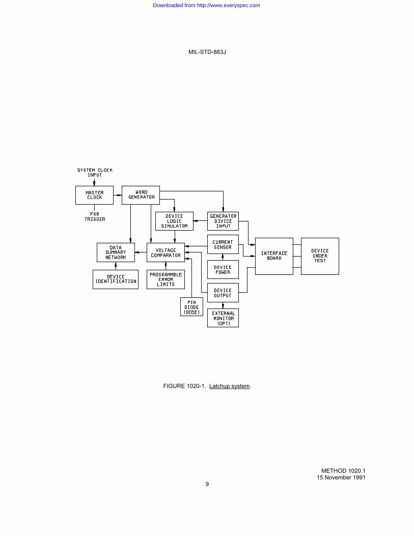
MIL-STD-883J
METHOD 1020.1 15 November 1991
9
FIGURE 1020-1. Latchup system.
Downloaded from http://www.everyspec.com
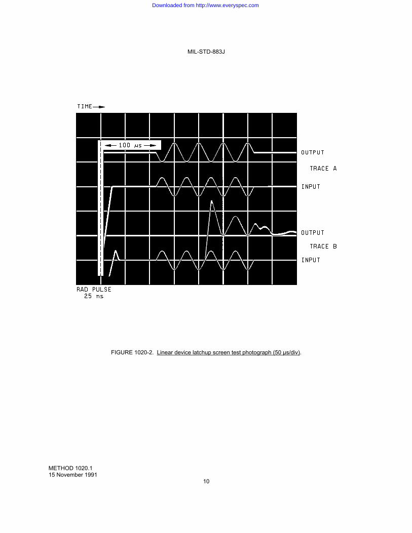
MIL-STD-883J
METHOD 1020.1 15 November 1991
10
FIGURE 1020-2. Linear device latchup screen test photograph (50 µs/div).
Downloaded from http://www.everyspec.com
MIL-STD-883J
METHOD 1021.3 26 February 2010
1
METHOD 1021.3 DOSE RATE UPSET TESTING OF DIGITAL MICROCIRCUITS 1. PURPOSE. This test procedure defines the requirements for testing the response of packaged digital integrated circuits to pulsed ionizing radiation. A flash x-ray or linear accelerator is used as a source of pulses of ionizing radiation. The response may include transient output signals, changes in the state of internal storage elements, and transient current surges at inputs, outputs, and power supply connections. The dose rate at which logic or change-of-state errors first occur is of particular interest in many applications. 1.1 Definitions. Definitions of terms used in this procedure are given below: a. Dose rate threshold for upset. The dose rate which causes either: (1) A transient output upset for which the change in output voltage of an operating digital integrated circuit goes
either above or below (as appropriate) specified logic levels (see 3.2 on transient voltage criteria), and the circuit spontaneously recovers to its preirradiation condition after the radiation pulse subsides, or
(2) A stored data or logic state upset for which there is a change in the state of one or more internal memory or
logic elements that does not recover spontaneously after the radiation pulse. However, the circuit can be restored to its preirradiation condition by applying the same sequence of logic signals to its inputs that were previously used to establish the preirradiation condition, or
(3) A dynamic upset which results in a change in the expected output or stored test pattern of a device that is
functionally operating during the time it is irradiated. The upset response may depend on the precise time relationship between the radiation pulse and the operating cycle of the device. For operations requiring many clock signals, it may be necessary to use a wide radiation pulse.
b. Dose rate. Energy absorbed per unit time per unit mass by a given material from the radiation field to which it is
exposed. c. Combinational logic circuit. A digital logic circuit with the property that its output state is solely determined by the
logic signals at its inputs. Combinational logic circuits contain no internal storage elements. Examples of combinational circuits include gates, multiplexers, and decoders.
d. Sequential logic circuit. A digital logic circuit with the property that its output state at a given time depends on the
sequence and time relationship of logic signals that were previously applied to its inputs. Sequential logic circuits contain internal storage elements. Examples of sequential logic circuits include memories, shift registers, counters, and flip-flops.
e. State vector. A state vector completely specifies the logic condition of all elements within a logic circuit. For
combinational circuits the state vector includes the logic signals that are applied to all inputs; for sequential circuits the state vector must also include the sequence and time relationship of all input signals (this may include many clock cycles).
Downloaded from http://www.everyspec.com
MIL-STD-883J
METHOD 1021.3 26 February 2010
2
1.2 Interferences. There are several interferences that need to be considered when this test procedure is applied. These include: a. Total dose damage. Devices may be permanently damaged by total dose. This limits the number of radiation
pulses that can be applied during transient upset testing. The total dose sensitivity depends on fabrication techniques and device technology. MOS devices are especially sensitive to total dose damage. Newer bipolar devices with oxide-isolated sidewalls may also be affected by low levels of total dose. The maximum total dose to which devices are exposed must not exceed 20 percent of the typical total dose failure level of the specific part type.
b. Steps between successive radiation levels. The size of the steps between successive radiation levels limits the
accuracy with which the dose rate upset threshold is determined. Cost considerations and total dose damage limit the number of radiation levels that can be used to test a particular device.
c. Latchup. Some types of integrated circuits may be driven into a latchup condition by transient radiation. If latchup
occurs, the device will not function properly until power is temporarily removed and reapplied. Permanent damage may also occur, primarily due to the large amount of localized heating that results. Although latchup is an important transient response mechanism, this procedure does not apply to devices in which latchup occurs. Functional testing after irradiation is required to detect internal changes of state, and this will also detect latchup. However, if latchup occurs it will usually not be possible to restore normal operation without first interrupting the power supply.
d. Limited number of state vectors. Cost, testing time, and total dose damage usually make it necessary to restrict
upset testing to a small number of state vectors. These state vectors must include the most sensitive conditions in order to avoid misleading results. An analysis is required to select the state vectors used for radiation testing to make sure that circuit and geometrical factors that affect the upset response are taken into account (see 3.1).
2. APPARATUS. Before testing can be done, the state vectors must be selected for radiation testing. This requires a logic diagram of the test device. The apparatus used for testing shall consist of the radiation source, dosimetry equipment, a test circuit board, line drivers, cables, and electrical test instrumentation to measure the transient response, provide bias, and perform functional tests. Adequate precautions shall be observed to obtain an electrical measurement system with ample shielding, satisfactory grounding, and low noise from electrical interference or from the radiation environment. 2.1 Radiation source. The radiation source used in this test shall be either a flash x-ray machine (FXR) used in the photon mode or a linear accelerator (LINAC) used in the electron beam mode. The LINAC beam energy shall be greater than 10 MeV. The radiation source shall provide a uniform (within 20 percent) radiation level across the area where the device and the dosimeter will be placed. The radiation pulse width for narrow pulse measurements shall be between 10 and 50 ns. For narrow pulse measurements either a LINAC or FXR may be used. Wide pulse measurements (typically 1 - 10 s) shall be performed with a LINAC. The pulse width for LINAC irradiations shall be specified. The dose rate at the location of the device under test shall be adjustable between 106 and 1012 rads(Si)/s (or as required) for narrow pulse measurements and between 105 and 1011 rads(Si)/s (or as required) for wide pulse measurements. Unless otherwise specified, a test device exposed to a total dose that exceeds 20 percent of the total dose failure level shall be considered as destructively tested and shall be removed from the lot (see 1.2a). 2.2 Dosimetry equipment. Dosimetry equipment must include a system for measuring total dose, such as a thermoluminescent dosimeter (TLD) or calorimeter, a pulse shape monitor, and an active dosimeter that allows the dose rate to be determined from electronic measurements, e.g., a p-i-n detector, Faraday cup, secondary emission monitor, or current transformer.
Downloaded from http://www.everyspec.com
MIL-STD-883J
METHOD 1021.3 26 February 2010
3
2.3 Test circuit. The test circuit shall contain the device under test, wiring, and auxiliary components as required. It shall allow for the application of power and bias voltages or pulses at the device inputs to establish the state vector. Power supply stiffening capacitors shall be included which keep the power supply voltage from changing more than 10 percent of its specified value during and after the radiation pulse. They should be placed as close to the device under test as possible, but should not be exposed to the direct radiation beam. Provision shall be made for monitoring specified outputs. Capacitive loading of the test circuit must be sufficiently low to avoid interference with the measurement of short-duration transient signals. Generally a line driver is required at device outputs to reduce capacitive loading. Line drivers must have sufficient risetime, linearity, and dynamic range to drive terminated cables with the full output logic level. The test circuit shall not affect the measured output response over the range of expected dose rates and shall not exhibit permanent changes in electrical characteristics at the expected accumulated doses. It must be shielded from the radiation to a sufficient level to meet these criteria. Test circuit materials and components shall not cause attenuation or scattering which will perturb the uniformity of the beam at the test device position (see 2.1 for uniformity). The device under test shall be oriented so that its surface is perpendicular to the radiation beam. 2.4 Cabling. Cabling shall be provided to connect the test circuit board, located in the radiation field, to the test instrumentation located in the instrumentation area. Coaxial cables, terminated in their characteristic impedance, shall be used for all input and output signals. Double shielded cables, triax, zipper tubing or other additional shielding may be required to reduce noise to acceptable levels. 2.5 Transient signal measurement. Oscilloscopes or transient digitizers are required to measure transient output voltages, the power supply current and the dosimeter outputs. The risetime of the measuring instrumentation shall be less than 10 ns for pulse widths greater than 33 ns or less than 30 percent of the radiation pulse width for pulse widths less than 33 ns. 2.6 Functional testing. Equipment is also required for functional testing of devices immediately after the radiation pulse in the radiation test fixture. This equipment must contain sources to drive inputs with specified patterns, and comparison circuitry to determine that the correct output patterns result. This equipment may consist of logic analyzers, custom circuitry, or commercial integrated circuit test systems. However, it must be capable of functioning through long cables, and must also be compatible with the line drivers used at the outputs of the device in the test circuit.
2.7 General purpose test equipment. Power supplies, voltmeters, pulse generators, and other basic test equipment that is required for testing is general purpose test equipment. This equipment must be capable of meeting the test requirements and should be periodically calibrated in accordance with ANSI/NCSL Z540.3 or equivalent. 3. PROCEDURE. An outline of the procedure is as follows: a) determine the state vectors (or sequence of test vectors for a dynamic test) in which the device will be irradiated; b) following the test plan, set up the test fixture, functional test equipment, and transient measurement equipment; c) set up and calibrate the radiation source; d) perform a noise check on the instrumentation; and e) test devices at a sequence of radiation pulses, determining the transient response at specified dose rates. The dose rate upset level can be determined by measuring the transient response at several dose rates, using successive approximation to determine the radiation level for dose rate upset. 3.1 State vector selection. Two approaches can be used to select the state vectors in which a device is to be irradiated: a. Multiple output logic states. Partition the circuit into functional blocks. Determine the logic path for each output,
and identify similar internal functions. For example, a 4-bit counter can be separated into control, internal flip-flop, and output logic cells. Four identical logic paths exist, corresponding to each of the four bits. Determine the total number of unique output logic state combinations, and test the circuit in each of these states. For the counter example this results in 16 combinations so that the upset must be determined for each of these 16 state vectors.
Downloaded from http://www.everyspec.com
MIL-STD-883J
METHOD 1021.3 26 February 2010
4
b. Topological analysis approach. If a photomicrograph of the circuit is available, the number of required states can
be reduced by examining the topology of the internal circuits. This allows one to eliminate the need to test paths with the same output state which have identical internal geometries. For the counter, this reduces the required number of states to two. This approach is recommended for more complex circuits where the multiple output logic approach results in too many required state vectors.
3.2 Transient output upset criteria. The transients that are permitted at logic outputs depend on the way that the system application allocates the noise margin of digital devices. Most systems use worst-case design criteria which are not directly applicable to sample testing because the samples represent typical, not worst-case parts, and have higher noise margins. For example, although the logic swing of TTL logic devices is typically greater than 2 volts, the worst-case noise margin is specified at 400 mV. In a typical system, much of this noise margin will be required for aberrations and electrical noise, leaving only part of it, 100 mV to 200 mV, for radiation-induced transients. Thus, the allowable voltage transient is far lower than the typical logic signal range. Loading conditions also have a large effect on output transients. However, transient upset testing is usually done at a fixed temperature under conditions that are more typical than they are worst-case. Thus, the noise margin during testing is much greater. The recommended default condition if not specified by the system is a transient voltage exceeding 1 V for CMOS or TTL logic devices with 5 V (nominal) power supply voltage, and 30 percent of the room-temperature logic level swing for other technologies such as ECL, open collector devices, or applications with other power supply voltages. Default loading conditions are minimum supply voltage and maximum fanout (maximum loading). The time duration of transient upset signals is also important. If the duration of the transient voltage change is less than the minimum value required for other circuits to respond to it, the transient signal shall not be considered an upset. The minimum time duration shall be one-half the minimum propagation delay time of basic gate circuits from the circuit technology that is being tested. Testing criteria may also be established for other parameters, such as the power supply current surge. Output current is also important for tri-state or uncommitted ("open-collector") circuits. These criteria must be specified by the test plan, and are normally based on particular system requirements. 3.3 Test plan. The test plan must include the following: a. Criteria for transient voltage upset, output current, and power supply current, as applicable. b. Power supply and operating frequency requirements. c. Loading conditions at the outputs. d. Input voltage conditions and source impedance. e. Functional test approach, including dynamic upset, if applicable. f. Radiation pulse width(s). g. Sequence used to adjust the dose rate in order to determine the upset threshold by successive approximation. h. State vectors used for testing (determined from 3.1). i. Radiation levels to be used for transient response measurements, if applicable. j. A recommended radiation level at which to begin the test sequence for transient upset measurements, if
applicable. k. The temperature of the devices during testing (usually 25°C ±5°C).
Downloaded from http://www.everyspec.com
MIL-STD-883J
METHOD 1021.3 26 February 2010
5
3.4 Test circuit preparation. The test circuit shall be assembled including a test circuit board, line drivers, electrical instruments, functional test equipment, transient measurement equipment, and cables to provide the required input biasing, output monitoring, and loading. 3.5 Facility preparation. The radiation source shall be adjusted to operate in the specified mode and provide a radiation pulse width within the specified width range. The required dosimeters shall be installed as close as practical to the device under test. If special equipment is needed to control the temperature to the value specified in the test plan, this equipment must be assembled and adjusted to meet this requirement. 3.6 Safety requirements. The health and safety requirements established by the local Radiation Safety Officer or Health Physicist shall be observed. 3.7 Test circuit noise check. With all circuitry connected, a noise check shall be made. This may be done by inserting a resistor circuit in place of the test device. Resistor values chosen shall approximate the active resistance of the device under test. A typical radiation pulse shall be applied while the specified outputs are monitored. If any of the measured transient voltages are greater than 10 percent of the expected parameter response, the test circuit is unacceptable and shall not be used without modification to reduce noise. 3.8 Bias and load conditions. Unless otherwise specified, the power supply shall be at the minimum allowed value. Input bias levels shall be at worst-case logic levels. Outputs shall be loaded with the maximum load conditions in both logic states (usually equivalent to maximum circuit fanout). 3.9 Temperature. The temperature of the devices during test should be measured with an accuracy of ±5°C unless higher accuracy is required in the test plan. 3.10 Procedure for dose rate upset testing. The device to be tested shall be placed in the test socket. The required pulse sequence shall be applied so that the device is in the state specified by the first of the state vectors in 3.1. a. Set the intensity of the radiation source to the first radiation test level specified in the test plan. Expose the device
to a pulse of radiation, and measure the transient output responses and power supply current transient. For sequential logic circuits, perform a dynamic functional test to see if changes occurred in internal logic states.
b. Repeat 3.10a for all other state vectors and radiation levels specified in the test plan. 3.11 Radiation exposure and test sequence for upset threshold testing. The device to be tested shall be placed in the test socket. The required pulse sequence shall be applied so that the device is in the state specified by the first of the state vectors determined in 3.1, or is operating with the specified test vector sequence for dynamic upset. a. Set the intensity of the radiation source to the initial level recommended in the test plan, and expose the device to
a pulse of radiation. Determine whether a stored data upset, logic state upset, or dynamic upset occurs, as appropriate.
b. If no upset occurred, increase the radiation level according to the sequence specified in the test plan; if an upset
is observed decrease the radiation level. After the radiation source is adjusted to the new intensity, reinitialize the part to the required state vector, expose it to an additional pulse, and determine whether or not upset occurred. Continue this sequence until the upset response threshold level is bracketed with the resolution required in the test plan.
c. The power supply peak transient current shall be monitored and recorded during radiation testing unless it is not
required by the test plan. d. Repeat test sequences 3.11a through 3.11c for all of the state vectors.
Downloaded from http://www.everyspec.com
MIL-STD-883J
METHOD 1021.3 26 February 2010
6
3.12 Report. As a minimum the report shall include the following: a. Device identification. b. Test date and test operator. c. Test facility, radiation source specifications, and radiation pulse width. d. Bias conditions, output loading, and test circuit. e. Description of the way in which state vectors for testing were selected. f. State vectors used for radiation testing and functional test conditions for each state vector. g. Criteria for transient output upset. h. Records of the upset threshold and power supply current for each state vector. i. Equipment list. j. Results of the noise test. k. Temperature (see 3.9). 4. SUMMARY. The following details shall be specified. a. Device type and quantity to be tested. b. Test circuit to be used, including output loading impedance. c. State vectors to be used in testing and device output pins to be monitored. d. Functional test sequence. e. Power supply voltage and bias conditions for all pins. f. Pulse width of the radiation source (see 2.1). g. The method of selecting steps between successive irradiation levels and the required resolution. h. Restrictions on ionizing (total) dose if other than that specified in 3.1. i. Temperature of the devices during testing. j. Requirement for measuring and recording power supply peak transient current (see 3.11c). k. Failure criteria for transient output voltage upset. l. Failure criteria for power supply current and output current, if applicable.
Downloaded from http://www.everyspec.com
MIL-STD-883J
METHOD 1022 4 November 1980
1
METHOD 1022 MOSFET THRESHOLD VOLTAGE 1. PURPOSE. This method establishes the means for measuring MOSFET threshold voltage. This method applies to both enhancement-mode and depletion-mode MOSFETs, and for both silicon on sapphire (SOS) and bulk-silicon MOSFETs. It is for use primarily in evaluating the response of MOSFETs to ionizing radiation, and for this reason the test differs from conventional methods for measuring threshold voltage. 1.1 Definition. 1.1.1 MOSFET threshold voltage, VTH. The gate-to-source voltage at which the drain current is reduced to the leakage current, as determined by this method. 2. APPARATUS. The apparatus shall consist of a suitable ammeter, voltmeters, and voltage sources. The apparatus may be manually adjusted or, alternatively, may be digitally programmed or controlled by a computer. Such alternative arrangements shall be capable of the same accuracy as specified below for manually adjusted apparatus. 2.1 Ammeter (A1). The ammeter shall be capable of measuring current in the range specified with a full scale accuracy of ±0.5 percent or better. 2.2 Voltmeters (V1 and V2). The voltmeters shall have an input impedance of 10 M or greater and have a capability of measuring 0 to 20 V with a full scale accuracy of ±0.5 percent or better. 2.3 Voltage sources (VS1 and VS2). The voltage sources shall be adjustable over a nominal range of 0 to 20 V, have a capability of supplying output currents at least equal to the maximum rated drain current of the device to be tested, and have noise and ripple outputs less than 0.5 percent of the output voltage. 3. PROCEDURE. NOTE: The absolute maximum values of power dissipation, drain voltage, drain current, or gate voltage specified in either
the applicable acquisition document or the manufacturer's specifications shall not be exceeded under any circumstances.
3.1 N-channel devices. 3.1.1 Test circuit. The test circuit shown on figure 1022-1 shall be assembled and the apparatus turned on. With the voltage sources VS1 and VS2 set to 0 volts, the MOSFET to be tested shall be inserted into the test circuit. The gate polarity switch shall be set to the appropriate position, and voltage source VS1 shall be set 1.0 V negative with respect to the anticipated value of threshold voltage VTH. Voltage source VS2 shall be adjusted until voltmeter V2 indicates the specified drain voltage VD. The current ID, indicated by ammeter A1, and the gate voltage VG, indicated by voltmeter V1, shall be measured and recorded. 3.1.2 Measurement of gate voltages. The measurement shall be repeated at gate voltages which are successively 0.25 volts more positive until either the maximum gate voltage or maximum drain current is reached. If the gate voltage reaches 0 volts before either of these limits has been reached, the gate polarity switch shall be changed as necessary and measurements shall continue to be made at gate voltages which are successively 0.25 volts more positive until one of these limits has been reached.
Downloaded from http://www.everyspec.com
MIL-STD-883J
METHOD 1022 4 November 1980
2
3.2 p-channel devices. 3.2.1 Test circuit. The test circuit shown on figure 1022-2 shall be assembled and the apparatus turned on. With the voltage sources VS1 and VS2 set to 0 volts, the MOSFET to be tested shall be inserted into the test circuit. The gate polarity switch shall be set to the appropriate position, and voltage source VS1 shall be set 1.0 V positive with respect to the anticipated value of threshold voltage VTH. Voltage source VS2 shall be adjusted until voltmeter V2 indicates the specified drain voltage VD. The current ID, indicated by ammeter A1, and the gate voltage VG, indicated by voltmeter V1, shall be measured and recorded. 3.2.2 Measurement of gate voltages. The measurement shall be repeated at gate voltages which are successively 0.25 volts more negative until either the maximum gate voltage or maximum drain current is reached. If the gate voltage reaches 0 volts before either of these limits has been reached, the gate polarity switch shall be changed as necessary and measurements shall continue to be made at gate voltages which are successively 0.25 volts more negative until one of these limits has been reached. 3.3 Leakage current. The leakage current shall be measured. 3.3.1 Drain voltage. The drain voltage shall be the value specified in 4b. 3.3.2 Gate voltage. The gate voltage shall be five volts different from the anticipated threshold voltage in the direction of reduced drain current. 3.4 Plot of gate voltage. The gate voltage, VG, shall be plotted versus the square-root of the drain current minus the leakage current, √ ID - IL. At the point of maximum slope, a straight line shall be extrapolated downward. The threshold voltage VTH is the intersection of this line with the gate voltage axis. Examples are shown on figure 1022-3. 3.5 Report. As a minimum, the report shall include the device identification, the test date, the test operator, the test temperature, the drain voltage, the range of gate voltage, the leakage current, and the threshold voltage. 4. SUMMARY. The following details shall be specified in the applicable acquisition document: a. Test temperature. Unless otherwise specified, the test shall be performed at ambient. b. Drain voltage. c. Maximum drain current. d. Range of gate voltage.
Downloaded from http://www.everyspec.com
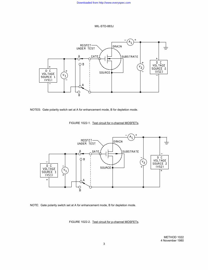
MIL-STD-883J
METHOD 1022 4 November 1980
3
NOTES: Gate polarity switch set at A for enhancement mode, B for depletion mode. FIGURE 1022-1. Test circuit for n-channel MOSFETs.
NOTE: Gate polarity switch set at A for enhancement mode, B for depletion mode. FIGURE 1022-2. Test circuit for p-channel MOSFETs.
Downloaded from http://www.everyspec.com
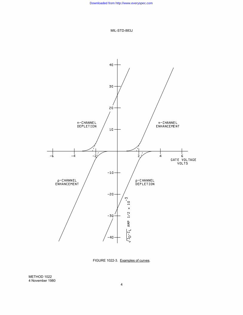
MIL-STD-883J
METHOD 1022 4 November 1980
4
FIGURE 1022-3. Examples of curves.
Downloaded from http://www.everyspec.com
MIL-STD-883J
METHOD 1023.3 26 February 2010
1
METHOD 1023.3
Dose Rate Response and Threshold for Upset of Linear Microcircuits
1. PURPOSE. This test procedure defines the requirements for measuring the dose rate response and upset threshold of packaged devices containing analog functions when exposed to radiation from a flash X-ray source or from a linear accelerator. This procedure addresses the measurement of dose rate response characteristics of a linear circuit, excluding latchup which is addressed in MIL-STD-883 Test Method 1020. 1.1 Definitions. The following are the definitions of terms used in this method: a. Dose rate response. The transient changes which occur in the operating parameters or in the output signal of an
operating linear microcircuit when exposed to a pulse of ionizing radiation. b. Dose rate. Energy absorbed per unit time and per unit mass by a given material from the radiation field to which it
is exposed. Units are specified in Gray (Gy) per second (s) in the material of interest, e.g., Gy(Si)/s, Gy(SiO2)/s, Gy(GaAs)/s, etc.
c. Dose rate induced upset. An upset has occurred when the radiation induced transient change in a specified
parameter (e.g., in output voltage, supply current, output signal waveform) exceeds a predetermined level. d. Upset threshold. The upset threshold is the minimum dose rate at which the device upsets. However, the
reported measured upset threshold shall be the maximum dose rate at which the device does not upset and which the transient disturbance of the output waveform and/or supply current remains within the specified limits.
1.2 Test plan. Prior to dose rate testing, a test plan shall be prepared which describes the radiation source, the dosimetry techniques, test equipment, the device to be tested, test conditions, and any unique testing considerations. A detailed procedure for each device type to be tested shall be prepared, either as part of the test plan, or in separate test procedure documents. The procedure shall include bias conditions, test sequence, schematics of the test setup and specific functions to be tested. The test plan shall be approved by the acquiring activity, and as a minimum, the items listed below shall be provided in the test plan or procedure: a. Device types, including package types, manufacturer, date codes, and quantities to be tested. b. Traceability requirements, such as requirements for serialization, wafer or lot traceability, etc. c. Requirements for data reporting and submission. d. Block diagram or schematic representation of test set up. e. List of equipment used in the testing and calibration compliance requirements as required. f. Test conditions, e.g., bias voltage, temperature, etc. g. Electrical parameters to be monitored and device operating conditions, including functional test requirements
before, during and after the radiation pulse. Test patterns to be used for devices with storage elements, or devices with input pattern sensitivity shall also be specified.
h. Group A electrical test requirements for pre- and post-dose rate testing, when applicable, to include test limits and
failure criteria. i. Radiation test parameters such as pulse width(s), radiation dose(s) per pulse and dose rate range(s). j. Total ionizing dose limit acceptable for each device type. k. Upset and failure criteria, e.g., effective number of bits (ENOB) or missing codes in analog to digital converters
(ADCs), delta VOH or Vref, time to recovery, output waveform distortion in shape or frequency, etc.
Downloaded from http://www.everyspec.com
MIL-STD-883J
METHOD 1023.3 26 February 2010
2
1.3 Formulation of the upset criteria. The upset criteria are usually generated from characterization data at the dose rate of interest. Upset criteria can sometimes be determined by analysis/simulation (SPICE or equivalent computer code) of the application circuit, if the code has been verified to agree with experimental data for similar circuits and exposure conditions. 1.4 Specification of the upset criteria. Once formulated, the upset criteria shall be specified in the detailed specification. The upset criteria may consist of the following (a waveform may be included denoting the acceptable boundaries): a. Measurement circuit to which criteria apply. b. Peak amplitude of tolerable transient change in output voltage. c. Allowable duration of transient output change (recovery time). d. Limiting value for the surge in power supply current and recovery characteristics. e. Steady state (return to normalcy) level of the output voltage following recovery. f. ENOB or missing codes for ADCs. g. Delta parameters such as Vref or VOH. h. Device saturation time.
2. APPARATUS. The apparatus shall consist of the radiation source, dosimetry equipment, remote test circuit to include signal recording devices, cabling, line drivers, interconnect fixture, and exposure board. Adequate precautions shall be observed to obtain an electrical measurement system with sufficient insulation, ample shielding, satisfactory grounding and low noise from electrical interference or from the radiation environment (see section 3.7.3).
2.1 Radiation Source. Either of two radiation sources shall be used for dose rate testing: 1) a flash x-ray machine (FXR), or 2) an electron linear accelerator (LINAC). The FXR shall be used in the x-ray mode and the LINAC in the electron (e-beam) mode. Unless otherwise specified, the FXR peak charging voltage shall be 2 MV or greater, and the LINAC beam energy shall be 10 MeV or greater. The uniformity of the radiation field in the device irradiation volume shall be + 15% as measured by the dosimetry system. The dose per radiation exposure shall be as specified in the test plan or procedure. 2.2 Dosimetry System. A dosimetry system shall be used which provides a measurement accuracy within + 15 percent. A calibrated PIN diode may be used to obtain both the shape of the radiation pulse and the dose. The following American Society for Testing and Materials (ASTM) standards or their equivalent may be used: ASTM F 526 Standard Method for Measuring Dose for Use in Linear Accelerator Pulsed Radiation Effects Tests. ASTM E 666 Standard Method for Calculation of Absorbed Dose from Gamma or X Radiation. ASTM E 668 Standard Practice for the Application of Thermo-luminescence Dosimetry (TLD) Systems for Determining Absorbed Dose in Radiation Hardness Testing of Electronic Devices. These methods describe techniques to determine the absorbed dose in the material of interest. Device packaging material and thickness should be considered in determining the dose to the DUT. For FXR tests, dose enhancement effects of the package shall be considered. Dosimetry techniques shall be reported in the test report as well as device packaging material, thickness and dose enhancement effects, if applicable.
Downloaded from http://www.everyspec.com
MIL-STD-883J
METHOD 1023.3 26 February 2010
3
2.3 Dose Rate Test System. The instrumentation shall be capable of establishing the required test conditions and measuring and recording the required parameters in the specified time frame. Components other than the device under test (DUT) shall be insensitive to the expected radiation levels, or they shall be shielded from the radiation. The system used for dose rate testing shall contain the following elements: 2.3.1 Remote Test circuit. The remote portion of the test circuit includes power sources, input and control signal generators, instrumentation for detecting, measuring and recording transient and steady state response, and may also include automated test equipment (ATE). The remote portion of the test equipment is shielded from radiation and from radiation induced electromagnetic fields. Specified signals shall be measured and recorded during the radiation pulse, and the logic pattern shall be verified after the pulse (when applicable). 2.3.2 Interconnect fixture. The interconnecting fixture is located in the radiation exposure chamber and is connected to the remote portion of the test circuit via the cabling system. It serves as a power and signal distribution box and contains the line drivers that buffer the various DUT output signals. The characteristics of the line drivers (e.g., linearity, dynamic range, input capacitance, transient response and radiation response) shall be such that they accurately represent the response of the DUT output. The interconnect fixture shall be located as close as practical to the exposure fixture, and must be appropriately shielded against scattered radiation fields so that radiation induced effects do not adversely affect the fidelity of the output response being measured. 2.3.3 Test circuit. The test circuit for each device type shall provide worst case bias and load conditions for the DUT, and shall enable in-situ functional testing of the DUT as specified in the test plan or procedure. The test circuit accommodates the DUT, output loads, and the supply stiffening capacitors connected directly to the DUT supply pins or its socket (see 2.3.4). To avoid ground loops, there shall be only one ground plane (or ground rings connected to a single ground) on the test circuit. Test Circuit parasitic resistance shall be kept to a minimum. 2.3.4 Stiffening capacitors. A high frequency capacitor shall be placed at each bias supply pin of the DUT with lead lengths as short as practicable. These capacitors should be large enough such that the power supply voltage drop at the DUT is less than 10% during the radiation pulse (typical values are between 4.7 and 10 µF). In parallel with this capacitor should be a low inductance capacitor (e.g., 0.1 µF), again as close as possible to the supply pin and with lead lengths as short as practical. In addition, for each supply line into the DUT, a larger capacitor, > 100 µF, may be placed a short distance away from the DUT and shielded from radiation. 2.3.5 Current Limiting Series resistor. A current limiting resistor in series with the power supply may only be used with prior approval of the acquiring activity. Note that a current limiting resistor may degrade the upset performance of the DUT. 2.3.6 Timing control. A timing control system shall be incorporated into the test system such that post-irradiation in-situ functional testing is performed at the specified time, and that recovery of the signal and supply current can be monitored. 2.4 Cabling. The remote test circuit shall be connected to the interconnect and exposure fixtures by means of shielded cables terminated in their characteristic impedance. Additional shielding provisions (e.g., doubly shielded cables, triax, zipper tubing, aluminum foil) may be required to reduce noise to acceptable levels. 2.5 Measuring and recording equipment. Oscilloscopes or transient waveform digitizers shall be used to measure and record the transient signal and the recovery period of the output voltage and supply current. The rise time of these instruments shall be such that they are capable of accurately responding to the expected pulse width(s). 3. PROCEDURE. 3.1 Device identification. In all cases, devices shall be serialized, and the applicable recorded test data shall be traceable to each individual device.
Downloaded from http://www.everyspec.com
MIL-STD-883J
METHOD 1023.3 26 February 2010
4
3.2 Radiation safety. All personnel shall adhere to the health and safety requirements established by the local radiation safety officer or health physicist. 3.3 Stress limits. 3.3.1 Total ionizing dose limit. Unless otherwise specified, any device exposed to more than 10% of its total ionizing dose limit shall be considered to have been destructively tested. The total dose limit shall be determined (or data obtained) for each device type to be tested. The total ionizing dose limit shall be specified in the test plan. 3.3.2 Burnout Limit. A device exposed to greater than 10% of the level at which photocurrent burnout occurs shall be considered destructively tested. The burnout level shall be specified in the test plan/procedure. The burnout level may be specified as the maximum dose rate level at which the device type has been tested and does not burnout. Note that dose rate testing causes surge currents ranging from 20 ns to 500 ns (typically) in duration, which may exceed the manufacturers' maximum ratings for current and power for that time period. 3.4 Characterization testing. Characterization tests shall be performed or data obtained to determine device performance as a function of dose rate and to establish requirements for production testing, if applicable. The following are examples of information gained from characterization testing: a. Parameter behavior over dose rate and pulse width. b. Upset threshold as a function of radiation dose rate and pulse width. c. Determination of susceptible circuit conditions. d. Identification of the most susceptible circuits of a device, and the appropriate outputs to monitor. e. Effect of temperature on upset or failure. f. Upset, recovery time and failure criteria to be specified in the device specification or drawing. g. Group A electrical parameter degradation subsequent to dose rate testing. h. Worst case power supply voltage. i. Maximum surge currents and duration, and photocurrent burnout level. 3.5 Production testing. Prior to production testing, characterization testing shall be performed or characterization data obtained for each device type. The results of the characterization tests (paragraph 3.4), or the existing data, will be used to develop the requirements for the production tests. These requirements are specified in the applicable test plan or procedure and include those items listed in paragraph 1.2. 3.5.1 General requirements for production tests. Production tests shall be performed at the specified dose rates (and pulse widths), with bias and load conditions as specified in the test plan or procedure. The measured response shall be compared to the upset criteria and determination of pass/fail shall be made. Devices having storage elements shall be loaded with the applicable test pattern prior to exposure and post-exposure functional test shall be performed to the extent necessary to verify the stored pattern. 3.6 Testing of Complex Linear Devices. Testing of complex linear devices, such as analog to digital and digital to analog converters, shall be performed using the necessary (as specified in the test plan or procedure) exposure conditions to ensure adequate coverage. Often, four or more exposure conditions are required. To the greatest extent practical, the most susceptible exposure conditions (i.e., most favorable for upset to occur) shall be used. For linear devices that have storage elements, each exposure state shall consist of a stored test pattern plus the external bias. Each test pattern shall be loaded prior to exposure, and following the application of the radiation pulse, functional testing of the device must be performed to the extent necessary to verify the pattern.
Downloaded from http://www.everyspec.com
MIL-STD-883J
METHOD 1023.3 26 February 2010
5
3.7 Dose Rate Test Sequence. 3.7.1 Facility Preparation. The radiation source shall be adjusted to operate in the specified mode and provide a radiation pulse within the specified pulse width range. The required dosimeters shall be installed as close as practical to the DUT. 3.7.2 Test Circuit preparation. The dose rate test system, including all test circuitry, cables, monitoring and recording equipment shall be assembled to provide the specified bias and load conditions and output monitoring. The test circuit shall be placed in position such that the DUT will receive the specified dose. Unless otherwise specified, dose rate testing shall be performed at 25 + 5C. (The test temperature shall be specified in the test plan/procedure.) 3.7.3 Test circuit noise check. With all circuitry connected, a noise check, including radiation induced noise, shall be made. Noise signals shall be kept as low as practicable. The circuitry and cabling system shall be modified until the noise signals are below an acceptable level (usually less than 10% of the expected response). 3.7.4 Test Procedure. CAUTION: Exercise caution when handling devices, particularly with regard to pin alignment in the and holding fixture and
when installing devices in the test circuit. Ensure that voltages are off before inserting the DUT. Observe ESD handling procedures for the class of devices being tested, as appropriate.
Step 1: Adjust timing control system to provide the required time interval between radiation pulse and
post-irradiation measurements. Step 2: Remove bias voltages and install a control sample device (same type as devices to be tested). Step 3: Turn on bias voltages and verify proper device function in accordance with performance
requirements. Step 4. Verify proper operation of all recording, monitoring and timing control equipment. Monitor and
record noise level and temperature. Step 5. Remove bias voltages and control device, in that order. Adjust the radiation source to operate in the specified mode to deliver the specified dose. Verify as follows: Step 6: Put dosimetry in position and expose to radiation pulse. Verify that the dose recording
equipment is working properly and that the appropriate dose was delivered. When the dose rate test system, radiation source and dosimetry system have been verified to be working properly, continue as follows for each device type to be tested: Step 7: Ensure bias is removed from the test circuit and install DUT. Step 8: Bias the device and load the test patterns (if applicable) in accordance with the test plan or
procedure. Verify proper device functional operation. Step 9: Expose the DUT to the radiation pulse and measure the response of the specified outputs, as well as the
recovery characteristics. Step 10: Compare the DUT response to upset criteria, if applicable. Repeat steps 8-10 for each exposure state and for each radiation dose rate. Step 11: Remove bias and DUT in that order. Note that the upset threshold shall be reported as the maximum dose rate at which the DUT does not upset.
Downloaded from http://www.everyspec.com
MIL-STD-883J
METHOD 1023.3 26 February 2010
6
4. Test Report. A dose rate test report shall be prepared and shall include the following (as a minimum):
a. Device identification, including manufacturer, wafer lot and/or inspection lot traceability information, pre-radiation history (e.g., class level S, class level B, prototype, etc).
b. Radiation test facility, type of source, pulse width, dosimetry data including pulse waveform. c. Test date, test operator's name and organization. d. Results of the noise test. e. Device response data, listed by device serial number, including output and supply recovery waveforms, and dose
per pulse for each device. f. Power supply droop during pulse. g. Post-exposure functional test data if applicable. h. All information included in the test plan/procedure (may be referenced or appended to test report), and any
deviations from the approved test plan/procedure. i. Package material and thickness, and effect of package material on dose to the device (see paragraph 2.2).
5. SUMMARY. The applicable device specification or drawing shall specify the following (as applicable): a. Device types and quantities to be tested. b. Traceability (device number, wafer/lot number, etc.) requirements and requirements for data reporting and
submission. c. Electrical configuration of the DUT during exposure (include schematic of exposure configuration). d. Sequence of exposure conditions and logical test patterns. e. Outputs to be monitored and recorded. f. Dose rate level(s) and pulse width(s). g. Criteria for upset and recovery, steady state value of recovered outputs and/or supply current. Include sample
waveforms if necessary. h. Upset threshold and failure level (if applicable). i. Post exposure functional test necessary to verify the stored pattern, and maximum time interval between
application of the radiation pulse and start of functional test. j. Total ionizing dose limit and burnout level for each device type. k. Maximum current limiting resistance in series with the power supply in the application (if applicable), and
allowable resistance in the test circuit (paragraph 2.3.5). l. Requirements for Group A electrical testing pre- and post-radiation testing, if applicable. m. Test instrument requirements, if other than those indicated above. n. Requirements for characterization, recharacterization and analysis.
Downloaded from http://www.everyspec.com
MIL-STD-883J
METHOD 1023.3 26 February 2010
7
APPENDIX A A1. This appendix provides an example of the specification of test details for an operational amplifier. Because the test conditions depend both on the type of device and on the specific application, this example shall not be considered as suitable for use in any given case. It is provided only as an illustration of the use of this test method. A2. Test specification, method 1023: a. Type 741 operational amplifier, in 8-pin TO-5 package. b. Test circuit as given on figure 1023-1. Leave pins 1, 5, and 8 unconnected. c. V+=9.0 + 0.2 V; V-=-9.0 + 0.2 V; input signal 280 mV +5% peak to peak, 2000 +50 Hz. d. Monitor pin 6 and the power supply current. e. Standard noise limits apply. f. Pulse width: 20 ns (Full width half maximum). g. Total Ionizing dose shall not exceed 10 Gy(Si). h. Test at a dose rate of 105 +30% Gy(Si)/s. i. Test temperature shall be ambient (25° +5°C). j. Pass/Fail Criteria: Power supply currents and the output signal shall return to within 10% of the pre-rad levels within 1 ms of the radiation pulse. k. This test is considered a destructive test.
Downloaded from http://www.everyspec.com
MIL-STD-883J
METHOD 1023.3 26 February 2010
8
FIGURE 1023-1. Example of test circuit for OP-AMP.
Downloaded from http://www.everyspec.com
MIL-STD-883J
METHOD 1023.3 26 February 2010
9
APPENDIX B
B1. This appendix provides an example of the specification of test details for an analog to digital converter (ADC). Because the test conditions depend both on the type of device and on the specific application, this example shall not be considered as suitable for use in any given case. It is provided only as an illustration of the use of this test method. B2. Test specification, method 1023: a. Type ADC (n=# bits=12), 40 pin ceramic DIP. b. The test circuit is given in Figure 1023-2, and an overview of the test setup is provided in Figure 1023-3. The storage RAM must write at a speed (taa>tclk) exceeding the DUT clock frequency, and provide an interface to
the controller, and be capable of storing a trigger pulse from the radiation source. Note that if the data ready line of the ADC is used, it must be monitored separately, as it may also upset.
c. A minimum of 3 input voltages shall be tested. Adjust input bias to center output code on: 1. Midscale (2n/2) 2. Fullscale - 10% (2n-0.1*2n) 3. Zero + 10% (0+0.1*2n) d. As a minimum, perform tests at 10 MHz and 1 MHz (Fmax and 0.1*Fmax). e. Upset Criteria: Determination of the upset threshold shall be determined by statistical analysis comparing the pre-
shot ADC output codes with the data taken during and immediately after the shot. The time to recover (within 20%) shall also be determined by comparing the pre-rad data with the post-rad data.
f. Pulse width: 20 ns (Full width half maximum). g. Test at dose rates ranging from 102 - 107 Gy(Si)/s to establish upset threshold. h. Total ionizing dose shall not exceed 500 Gy(Si). i. Test at ambient temperature (25° +5°C). j. After completion of the upset tests, test up to the machine maximum dose rate to determine if devices burn out.
This test is a destructive test.
Downloaded from http://www.everyspec.com
MIL-STD-883J
METHOD 1023.3 26 February 2010
10
FIGURE 1023-2. Example of test circuit for ADC (C1 = 4.7 µF, C2 = 0.1 µF).
Downloaded from http://www.everyspec.com
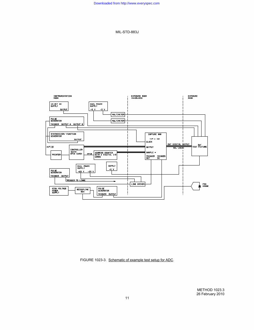
MIL-STD-883J
METHOD 1023.3 26 February 2010
11
FIGURE 1023-3. Schematic of example test setup for ADC.
Downloaded from http://www.everyspec.com
MIL-STD-883J
METHOD 1023.3 26 February 2010
12
This page intentionally left blank
Downloaded from http://www.everyspec.com
MIL-STD-883J
METHOD 1030.2 18 June 2004
1
METHOD 1030.2 PRESEAL BURN-IN 1. PURPOSE. The purpose of preseal burn-in is to identify marginal devices or stabilize monolithic, hybrid, or multichip microcircuits prior to the sealing of packages so that rework or retrimmings can be performed. Standard or sealed-lid burn-in testing (see method 1015) is designed to screen or eliminate marginal devices by stressing microcircuits at or above maximum rated operating conditions or by applying equivalent screening conditions which will reveal time and stress failure modes with equal or greater sensitivity. Performance of a portion of the standard burn-in testing prior to sealing will identify marginal devices or those requiring retrimming at a point where rework or retrimming can readily be performed. Use of preseal burn-in is optional and should be a function of the complexity of the microcircuit in question coupled with, if available, actual sealed-lid burn-in failure rates. 2. APPARATUS. Details for the required apparatus and compensation for air velocity, when required, shall be as described in method 1005. In addition, the oven used for preseal burn-in shall be so equipped to provide a dry (less than 100 ppm moisture, at the supply point) nitrogen at 100,000 (0.5 μm or greater) particles/cubic foot controlled environment (class 8 of ISO 14644-1). Suitable equipment shall be provided to control the flow of dry nitrogen and to monitor the moisture content of the dry nitrogen flowing into the oven.
3. PROCEDURE. All microcircuits shall be subjected to the specified preseal burn-in test condition (see 3.1) for the time and temperature and in the environment specified after all assembly operations, with the exception of lid sealing, have been completed (see method 5004 herein, MIL-PRF-38534 or MIL-PRF-38535); internal visual inspection shall be performed prior to sealing. The microcircuits shall be mounted by the leads, stud, or case in their normal mounting configuration, and the point of connection shall be maintained at a temperature not less than the specified ambient temperature. Measurements before and after preseal burn-in shall be made as specified. 3.1 Test conditions. Basic test conditions are as shown below. Details of each of these conditions shall be as described in method 1005. a. Test condition C: Steady-state dc voltages. b. Test condition D: Series or parallel excitation with ac conditions as applicable to exercise the device under test to
normal operating conditions. 3.1.1 Test time. Unless otherwise specified, preseal burn-in shall be performed for a minimum of 48 hours. It shall be permissible to divide the total minimum burn-in time between preseal and postseal burn-in provided that the total burn-in time equals or exceeds the specified burn-in time of 160 hours and that the postseal burn-in time equals or exceeds 96 hours. 3.1.2 Test temperature. Unless otherwise specified, the preseal burn-in test temperature shall be 125°C. If a lower temperature is used, a corresponding increase in time is necessary as shown on figure 1015-1. 3.1.3 Test environment. Preseal burn-in shall be performed in a dry nitrogen (less than 100 ppm moisture, at the supply point), 100,000 (5 µm or greater) particles/cubic foot controlled environment (class 8 of ISO 14644-1). Prior to heat-up, the oven shall be purged with dry nitrogen and then the bias shall be applied. Testing shall not commence until the specified environment has been achieved. 3.2 Measurements. Measurements before preseal burn-in, shall be conducted prior to applying preseal burn-in test conditions. Unless otherwise specified, measurements after preseal burn-in shall be completed within 96 hours after removal of the microcircuits from the specified pre-seal burn-in test condition and shall consist of all 25°C dc parameter measurements (subgroup A-1 of method 5005) and all parameters for which delta limits have been specified as part of interim electrical measurements. Delta limit acceptance, when applicable, shall be based upon these measurements. If these measurements cannot be completed within 96 hours, the microcircuits shall be subjected to the same specified test conditions (see 3.1) previously used for a minimum of 24 additional hours before measurements after pre-seal burn-in are made.
Downloaded from http://www.everyspec.com
MIL-STD-883J
METHOD 1030.2 18 June 2004
2
3.2.1 Cooldown after preseal burn-in. All microcircuits shall be cooled to within 10°C of their power stable condition at room temperature prior to the removal of bias. The interruption of bias for up to 1 minute for the purpose of moving the microcircuits to cool-down positions separate from the chamber within which testing was performed shall not be considered removal of bias. Alternatively, except for linear or MOS devices (CMOS, NMOS, PMOS, etc.) the bias may be removed during cooling provided the case temperature of microcircuits under test is reduced to a maximum of 35°C within 30 minutes after the removal of the test conditions. All 25°C dc measurements shall be completed prior to any reheating of the microcircuits.
3.2.2 Failure verification and repair. Microcircuits which fail the 25°C dc measurements after preseal burn-in shall be submitted for failure verification in accordance with test condition A of method 5003. After verification and location of the defective or marginal device in the microcircuit, rework shall be performed as allowed in MIL-PRF-38535 or MIL-PRF-38534. Upon completion of rework, repaired microcircuits shall be remeasured and, if found satisfactory, shall be returned for additional preseal burn-in (see 3.1) if such rework involved device replacement. 3.2.3 Test setup monitoring. The test setup shall be monitored at the test temperature initially and at the conclusion of the test to establish that all microcircuits are being stressed to the specified requirements. The following is the minimum acceptable monitoring procedure: a. Device sockets. Initially and at least each 6 months thereafter, each test board or tray shall be checked to verify
continuity to connector points to assure that bias supplies and signal information will be applied to each socket. Except for this initial and periodic verification, each microcircuit socket does not have to be checked; however, random sampling techniques shall be applied prior to each time a board is used and shall be adequate to assure that there are correct and continuous electrical connections to the microcircuits under test.
b. Connectors to test boards or trays. After the test boards are loaded with microcircuits and are inserted into the
oven, and prior to the nitrogen purge, each required test voltage and signal condition shall be verified in at least one location on each test board or tray so as to assure electrical continuity and the correct application of specified electrical stresses for each connection or contact pair used in the applicable test configuration.
c. At the conclusion of the test period, after cool-down, the voltage and signal condition verification of b above shall
be repeated. Where failures or open contacts occur which result in removal of the required test stresses for any period of the required test duration (see 3.1), the test time shall be extended to assure actual exposure for the total minimum specified test duration. 3.3 Handling of unsealed microcircuits. It is recommended that unsealed microcircuits be covered at all times for protection from handling induced defects. Snap-on metal covers, or rigid plastic covers with a conductive coating, may be removed from the microcircuits after all microcircuits are in place in the burn-in racks. Covers, if removed shall be replaced immediately after bias removal and completion of burn-in and cool-down prior to removal of microcircuits from the burn-in racks. Regardless of the method of handling during the time period between the completion of internal visual inspection following preseal burn-in and sealing, the microcircuits shall be retained in a controlled environment (see method 2017).
3.4 Sealed-lid burn-in. After completion of preseal burn-in, internal visual, other preseal screens and sealing all microcircuits shall undergo the screening specified in method 5004 herein, MIL-PRF-38534 or MIL-PRF-38535 except that stabilization bake may be deleted. Sealed-lid burn-in shall be performed as specified in method 5004 herein , MIL-PRF-38534 or MIL-PRF-38535 (see method 1015 for test details).
Downloaded from http://www.everyspec.com
MIL-STD-883J
METHOD 1030.2 18 June 2004
3
4. SUMMARY. The following details shall be specified in the applicable acquisition document. a. Test condition letter and burn-in circuit with requirements for inputs, outputs, applied voltages and power
dissipation as applicable (see 3.1). b. Test mounting, if other than normal (see 3). c. Pre and post preseal burn-in measurement and shift limits, as applicable (see 3.2). d. Time within which post preseal burn-in measurements must be completed if other than specified (see 3.2). e. Type of covers used to protect microcircuits from handling induced defects (see 3.3). f. Test duration for preseal and sealed lid burn-in (see 3.1.1). g. Test temperature, if less than 125°C (see 3.1.2).
Downloaded from http://www.everyspec.com
MIL-STD-883J
METHOD 1030.2 18 June 2004
4
This page intentionally left blank
Downloaded from http://www.everyspec.com
MIL-STD-883J
METHOD 1031 25 August 1983
1
METHOD 1031 THIN FILM CORROSION TEST
1. PURPOSE. The thin film corrosion test is performed for the purpose of demonstrating the quality or reliability of devices subjected to the specified conditions over a specified time period. This sample test is to be applied as either a short term specialized quality assurance test or as a long term acceleration test to assure device reliability. It is particularly suited to devices containing thin film conductors, resistors, or fuses which are susceptible to corrosion as a result of cavity water vapor which is less than the limits specified in methods 5005 herein and MIL-PRF-38534. Because of the destructive nature of the test, it should not be used as a 100 percent screen. It is the intent of this test to reveal time and temperature, stress dependent, moisture related failure modes resulting from metallization corrosion. 2. APPARATUS. Suitable sockets or other mounting means shall be provided to make firm electrical contact to the terminals of devices under test in the specified circuit configuration. Power supplies and a temperature chamber shall be capable of maintaining the specified operating conditions as a minima throughout the testing period. The test chamber shall be conditioned with dry air to prevent the test ambient from reaching 100 percent relative humidity during temperature cycling. 3. PROCEDURE. The microcircuits shall be subjected to the specified conditions, duration, and temperature, and the required measurements shall be made at the conclusion of the test. The test conditions, duration, quantity, and temperature shall be recorded and shall govern for the entire test. All programmable devices processed by the manufacturer to an altered item drawing shall be programmed prior to the test. 3.1 Test conditions. 3.1.1 Device conditioning. All devices shall be conditioned, without bias at 125°C ±10°C for a minimum of 24 hours before proceeding with the test. 3.1.1.1 Short term testing. For short term quality assurance testing the time-temperature bias sequence of figure 1031-1 shall be followed for 16 cycles, 3 hours each, for a total of 48 hours. The following sequence shall be used for the short term test:
Initial conditioning drives out deeply trapped water into ambient Step AB 125°C: Activate surface water from walls. Step BC Freeze out ambient water on walls and chip (temperature ramp 100°C/minute). Step CD Allow surface temperatures inside package to come to equilibrium (i.e., redistribute water). Step DE Transfer water from walls to chip (cold surface pump). At point E apply bias while chip is wet. Step EF Adjust temperature ramp so that chip is always the coldest temperature by minimizing heat
dissipation and adjusting temperature ramp (maximum 100°C/minute). Step FG Maintain 2°C ambient to insure highest R.H. near chip while bias is still applied. Step GH Heat quickly to evaporate water from walls, possibly with explosive force to enhance
contaminant transfer from the walls to the chip (maximum 100°C/minute). Temperature test cycle at 25°C when bias is applied. Remove from test fixture.
Downloaded from http://www.everyspec.com
MIL-STD-883J
METHOD 1031 25 August 1983
2
3.1.1.2 Long term testing. For long term reliability assurance testing the following modifications shall be made: Step AB Increased to 12 hours. Step CD Increased to 1 hour. Step DE Remains the same one-half hour. Step EG Bias applied at pt E and then cycled 30 minutes on, 30 minutes off during FG. Total time 24
hours. Step EF May be extended to 4 hours if power dissipation can be minimized. Step FG Increased to 6.5 hours. Total test time 10 weeks or 70 cycles. Terminate test cycle at 25°C when bias is applied. Remove from test fixture. 3.2 Measurements. Unless otherwise specified, all electrical measurement shall be completed within 12 hours after removal from the specified test conditions. End point measurements shall consist of group A, subgroups 1 and 7 at 25°C. NOTE: Method 1014 fine and gross leak test must be accomplished before 3.1.1 and after 3.2. Any circuit failing the leak
test will be removed from the test lot.
4. SUMMARY. The following details shall be provided in the applicable device specification or drawing: a. The electrical test configuration. b. The number of devices to be tested and the acceptance criteria. c. Requirements for data recording, when applicable.
Downloaded from http://www.everyspec.com
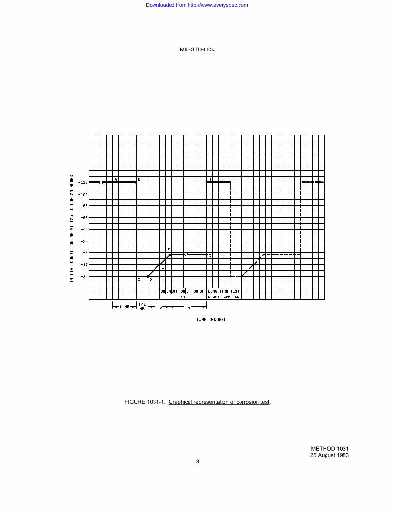
MIL-STD-883J
METHOD 1031 25 August 1983
3
FIGURE 1031-1. Graphical representation of corrosion test.
Downloaded from http://www.everyspec.com
MIL-STD-883J
METHOD 1031 25 August 1983
4
This page intentionally left blank
Downloaded from http://www.everyspec.com
MIL-STD-883J
METHOD 1032.1 29 May 1987
1
METHOD 1032.1 PACKAGE INDUCED SOFT ERROR TEST PROCEDURE (DUE TO ALPHA PARTICLES) 1. PURPOSE. This test method defines the procedure for testing integrated circuits under known test conditions for susceptibility to alpha induced errors. This test was specifically designed to measure the device's ability to withstand alpha particle impact. In addition, the procedure will determine the effectiveness of a "die-coating" shield. The test objective is to determine the rate that failures are induced due to alpha radiation sourced from the device package, die and die-coat material. 1.1 Definitions. The following definitions were created to be specific and relevant within the confines of this method. 1.1.1 DUT. Device under test. 1.1.2 Soft error. Any error induced by alpha particle impact resulting in either a transient error or an error in data storage witnessed at the DUT's output. 1.1.3 Source. A foil of Thorium-232. (Note: This foil generates particles which have an alpha energy spectrum of 0 through 10 MeV). 1.1.4 Soft error rate (SER). Failures per unit time under normal conditions of package environment. 1.1.5 Accelerated soft error rate (ASER). Failures per unit time induced by exposure to a known alpha particle source. 1.1.6 Failure in time (FIT). 1 FIT = 1 failure in 109 device-hours. 1.1.7 Package flux. The total number of alpha particles impinging on the die surface per unit of time and area, due to package material impurities (i.e., lid, die material, sealants, and optional alpha barrier material). Normal units of measurement: alpha/cm2-hr. 1.1.8 Modified package flux. The total number of alpha particles impinging on the die surface per unit of time and area, when a die coat is in place. Normal units of measurement: alpha/cm2-hr. 1.1.9 Source flux. The total number of alpha particles impinging on the die surface per unit of time and area, due to the calibrated source. Normal units of measurement: alpha/cm2-s. 2. APPARATUS. The apparatus will consist of electrical test instrumentation, test circuit board(s), cabling, interconnect boards, or switching systems and a Thorium-232 foil (optional). Precautions will be observed to obtain an electrical measurement system with adequate shielding, low electrical noise induction, and proper grounding. 2.1 Radiation source. The radiation source used in this test shall be a Thorium-232 foil with dimensions large enough to cover the entire exposed die cavity. The plated source shall be within the range of 0.01 - 5.0 Ci and shall produce the same energy spectrum as the package impurities. Radiation sources must be controlled according to state and federal regulations. The sources shall be certified periodically and decay rates used to determine the actual flux values at the time of use. This source must be processed at least one year before being used. Caution: These sources should not be exposed to heat.
2.2 Electrical test instruments. Electrical test instruments will be standard test instruments normally used for testing the DUT. They must be capable of establishing the required test conditions and measuring the required electrical parameters. All instruments shall be periodically calibrated in accordance with the general requirements of this test method standard.
Downloaded from http://www.everyspec.com
MIL-STD-883J
METHOD 1032.1 29 May 1987
2
2.3 Test circuits. The test circuit shall contain the DUT, wiring, and auxiliary components as required. Connection will allow for the application of the specified test conditions to obtain the specified outputs. Provision will be made for monitoring and recording the specified outputs. Any loading of the output(s), such as resistors or capacitors, shall be specified. The test circuit must not exhibit permanent changes in electrical characteristics as a result of exposure to the radioactive source. Shielding will be incorporated to prevent such effects from occurring if necessary. 2.4 Cabling. Cabling, if required, shall be provided to connect the test circuit board containing the DUT to the test instrumentation. All cables will be as short as possible. Care will be exercised to reduce electrical noise induced by the cable by using shielded cable, triax, zipper tubing, or other shielding methods. 3. PROCEDURES. Two methods of testing are allowed by this procedure. The first is a long term test (sometimes referred to as a system test) which does not incorporate a source but which accumulates a statistically valid amount of test time to determine the SER directly. This method is self explanatory and must be accomplished using the same parameters outlined in 3.1 (test plan). To determine the SER from this method, the following formula should be used and the result converted to FIT's. SER = Total number of errors/Total test time The second method incorporates the use of the source outlined in 2.1 (radiation source). The procedure for testing with an accelerated flux provided by the source is given below. These steps will be followed for each test outlined in 3.1. a. The flux that the surface of the die would receive without a die coat will be determined. This is designated as the
package flux. b. If the device has a die-coat it should be left in place for the next portion of the test. The DUT will be delidded and
the source placed directly over the die cavity at the same distance as the package lid was from the die.
NOTE: The distance between the foil and the die must be less than 50 mils and the foil must cover the entire die-cavity opening in order to assure all angles of incidence will be maintained.
NOTE: If the DUT has an inverted die configuration (e.g., flip-chip) a test jig must be implemented which will
expose the active surface of the die to the irradiating source. c. The testing outlined in 3.1 will be performed at this time with the configuration in b. above, in order to determine
the SER for each test performed. d. Recorded for each test performed will be the following: (1) Total number of errors recorded during each test. (2) Time to accumulate the errors. (3) SER1, calculated from the following formulas: ASER1 = Total number of errors/test time SER1 = ASER1 x (Package flux/source flux) e. If no die-coating has been applied, the SER1 will be reported as the measured rate of failure. However, if a die
coat exists, steps 3.f through 3.j will also be performed.
Downloaded from http://www.everyspec.com
MIL-STD-883J
METHOD 1032.1 29 May 1987
3
f. The flux at the surface of the die will be determined when the die coat is in place; this is designated as the
modified package flux.
NOTE: The modified package flux should be the sum of the flux from the die and die-coat material only. g. The die coat should be removed, assuring that no damage to the die has occurred and the source placed as
described in step b. h. The tests performed in step 3.c must be repeated with this configuration, and the new SER will be designated
SER2. i. Recorded for each test performed will be the following: (1) Total number of errors recorded during each test. (2) Time to accumulate the errors. (3) SER (SER2), calculated from the following formulas: ASER2 = Total number of errors/test time SER2 = ASER2 x (Modified package flux/source flux) j. The SER for the corresponding tests will be summed and reported as the rate of failure for this DUT, using the
following formula: SER = SER1 + SER2 NOTE: The order of the steps above can be reversed to enable testing before the die coat is applied and then after it has
been applied, if desired. 3.1 Test plan. A test plan will be devised which will include determination of the worst case operating environment of the DUT to determine the worst case SER, incorporating the steps outlined above. The data patterns used will ensure that each cell and path, or both, is tested for both the logic zero and logic one states. The device will be continuously monitored and refreshed and the data errors counted. This test will be required for each new device type or design revisions. The source value and exposure time will be sufficient to obtain a significant number of soft error failures. NOTE: If a data-retention or a reduced supply mode is a valid operating point for the DUT, this condition must also be
tested for its SER. 3.1.1 The test equipment program. The test equipment program will be devised to cycle and refresh the stored data or cycled pattern continually, recording the number of errors. 3.1.2 Test conditions. Testing shall be performed at three separate cycle rates and at minimum and maximum voltages. Unless otherwise specified, the following cycle timing will be used: The minimum and the maximum specified cycle timing and the midpoint between the minimum and maximum specified cycle timing. NOTE: If the device is a static or dynamic random access memory device, the device will be tested under both read and
write operations. 3.2 Report. As a minimum, the report will include device identification, test date, test operator, test facility (if applicable), radiation source, test cycle times and voltages, data analysis, and equipment used in the test.
Downloaded from http://www.everyspec.com
MIL-STD-883J
METHOD 1032.1 29 May 1987
4
4. SUMMARY. The following details shall be specified. a. Device type and quantity to be tested. b. Test circuit to be used. c. Device output pins to be monitored. d. Alpha source used if other than specified herein. e. Alpha source Curie level. f. Package flux measurement techniques. g. Test equipment to be used. h. Procedures for proper handling of radioactive materials.
Downloaded from http://www.everyspec.com
MIL-STD-883J
METHOD 1033 29 May 1977
1
METHOD 1033 ENDURANCE LIFE 1. PURPOSE. Endurance life is performed in order to demonstrate the quality and reliability of nonvolatile memory devices subjected to repeated write/erase cycles. This method may also be used in a screening sequence or as a preconditioning treatment prior to conducting other tests. It may be desirable to make end point, and where applicable, intermediate measurements on a serialized device basis or on the basis of a histogram distribution by total sample in order to increase the sensitivity of the test to parameter degradation or the progression of specific failure mechanism with cycles, time, or temperature. 1.1 Terms and definitions. 1.1.1 Endurance. The number of write/erase cycles a device can tolerate before failing to perform to specification. 1.1.2 Write/erase cycle. The act of changing the data from original to opposite to original in all bits of a memory device. This may be done for all bits in parallel or serial, e.g., block, byte, or bit. 1.1.3 Data retention screen. The unbiased baking at high temperature to accelerate the loss of charge from the storage node. 2. APPARATUS. The apparatus required for this test shall consist of equipment capable of write/erase cycling the devices, a controlled temperature chamber for performing a data retention bake, and suitable electrical test equipment to make the specified interim and end point measurements. 3. PROCEDURE. The devices shall be write/erase cycled (all bits) for specified maximum number of cycles, followed by electrical test, the specified data retention bake and electrical test. Interim pull points shall use the same sequence of cycle, electrical test, data retention bake, and electrical test.
3.1 Test condition. The case temperature, cycle time, data retention bake, and electrical test temperatures and conditions will be specified in the applicable device specification or drawing (see 4).
3.2 Failure criteria. No device is acceptable that exhibits: a. Inability to write or erase across the temperature range. b. Inability to retain data. c. Inability to read at specified timing conditions, across the temperature and supply voltage range. d. Inability to be write/erase cycled a minimum number of times n.
Downloaded from http://www.everyspec.com
MIL-STD-883J
METHOD 1033 29 May 1977
2
4. SUMMARY. The following details shall be specified in the applicable acquisition document: a. Number of write/erase cycles, n. b. Data retention bake conditions, including duration and temperature. c. Electrical test case temperature and timing conditions. d. Requirements for preconditioning, if applicable, and procedure if different than in 3. e. Cycle conditions including temperature, type (e.g., block, byte, or bit) and write/erase pulse duration and repetition
rate. f. The sample plan including number of devices to be cycled and acceptance number. g. End-point and interim electrical test criteria.
Downloaded from http://www.everyspec.com
MIL-STD-883J
METHOD 1034.1 18 June 2004
1
METHOD 1034.1
DYE PENETRANT TEST
1. PURPOSE. This method tests the capability of a Plastic Encapsulated Microcircuit (PEM) to withstand moisture ingress and to detect flaws in packaging materials.
2. APPARATUS. The apparatus for the Dye Penetrant test shall be as follows. a. Protective absorbent mats (paper/plastic)
b. 2 2000 ml containers
c. 2 1000 ml beakers
d. 2 mixing magnets
e. 2 hot plates for mixing
f. Whatman 42 filters (0.005)
g. 500 ml funnel h. Fisher bell jar with stopper
i. Filtration base with vacuum accessories (fisher allied filtrator #9-788 11 cm base)
j. Vacuum pump, hoses, and clamps k. 15 ml beaker
l. 50 ml beaker
m. 2 250 ml beakers n. Watchglass or evaporating dish
o. Petri dish
p. Drummond 0.1 ml pipettes and plunger
q. Graduated cylinder
r. Vacuum oven
s. Heating oven
t. B1 filter / polyvar (or olympus PMG3 inverted microscope)
u. 52 film - 400 ASA
v. 57 film - 3000 ASA
3. PROCEDURES. The following procedures shall be followed in performing the Dye Penetrant test. This technique
utilizes a low viscosity, anaerobic liquid penetrant (Resinol) which is mixed with a fluorescent powder (Yellow Dye G) and a anaerobic accelerator (17724). NOTE: These chemicals are skin, eye and nose irritants.
Downloaded from http://www.everyspec.com
MIL-STD-883J
METHOD 1034.1 18 June 2004
2
3.1 Dye penetration procedure outline. a. Mix dye solution.
Loctite Resinol RTC 18018 Loctite Accelerator for PMS 17724 Morton Fluorescent Yellow G Note: Solutions with an established or verifiable equivalent makeup and performance may be used.
b. Place the parts in a beaker of the dye solution. c. Place the beaker in the vacuum oven. d. Leave the beaker for 15 minutes at a vacuum of 1 to 0.3 torr. e. Bring the vacuum oven back to atmospheric pressure, then wait 15 minutes. f. Remove the parts from the dye solution. g. Wipe off the parts to remove the excess dye. h. Heat the parts in the oven at 100C for 1 hour to harden the polymer mixture. i. Mount the parts for cross-sectioning. j. Cross-section the parts. k. View the parts under magnification. l. Take an optical photo of the cross-section. m. Take a photo of the cross-section under UV to document the depth of penetration. NOTE: Lay down a double layer of protective mats before starting this procedure. The dye spreads and stains quite
easily. Be sure to wear the appropriate protective apparel, which includes chemical gloves, goggles, and a lab coat.
3.1.1 PREMIX solution preparation. Prepare a stock solution (PREMIX solution) of the resinol and yellow dye.
3.1.1.1 Mixing the solution. A mixture of 100 parts resinol to 1 part yellow dye powder is required to make the PREMIX
solution. a. Measure and pour 2000 ml of resinol into a beaker. b. Measure 20 g of yellow dye and pour it into the 2000 ml of resinol. Stir this mixture for 5 minutes, then separate
the mixture into two 1000 ml beakers to make it easier to work with. Place a mixing magnet in each of the beakers, then place the beakers on mixing plates. Stir the mixtures for two to three hours.
3.1.1.2 Filtering the PREMIX. The PREMIX must be filtered to ensure that any undissolved particles are removed from
the solution. a. Take a WHATMAN 42 filter and place it in the 11 cm Buckner funnel. Place the funnel adapter on the stem of the
funnel. Then place the funnel into the top of the bell jar. Place a 250 ml beaker on the bell jar base. Place the bell jar and funnel over the beaker on the bell jar base.
b. Turn on the vacuum pump.
Downloaded from http://www.everyspec.com
MIL-STD-883J
METHOD 1034.1 18 June 2004
3
c. Take one of the 1000 ml beakers of premix and pour about 200 ml of the premix into the funnel. When the
solution has drained through the funnel, turn off the vacuum pump, and pour the filtered solution into an empty container marked "RESINOL AND YELLOW DYE G MIXTURE". Repeat this process until all of the solution is filtered.
d. Remove the filter and replace it with a new one. e. Repeat step 3 with the second 1000 ml beaker of solution. f. Wash the beakers in a soap and water solution.
3.1.2 Setup of PREMIX and accelerator. A mixture of 200,000 parts PREMIX to 1 part accelerator is required. Due to the small amount of accelerator required, the mixture of premix and accelerator is performed in two steps. First a 200:1 mixture is prepared, then a 1000:1 mixture is made utilizing the 200:1 solution in order to achieve a 200,000:1 mixture. a. Measure out 10 ml of premix (resinol/yellow dye stock solution) with a graduated cylinder. Pour the 10 ml into a
small beaker. b. Insert the Drummond pipette and plunger into the accelerator solution. The glass pipette has two green markings.
The first marking is 0.05 ml, and the second marking is 0.1 ml. c. Draw up 0.05 ml (1st green mark) of accelerator, and mix it into the 10 ml of premix. d. Place a mixing magnet into the solution, and place the beaker on the mixing plate. Stir the solution for 5 minutes.
This completes the mixing of the 200:1 premix:accelerator solution.
e. Clean the pipette and plunger in a soap and water solution. They must be clean when they are used in step h. f. Fill a graduated cylinder with the amount of premix (resinol/yellow dye solution) that is needed to submerse the
devices requiring dye penetration. Most jobs will require 25 ml of solution. The amount will vary depending upon the number and size of the devices in the job.
g. Pour the 25 ml of premix (or the desired amount) into a small beaker. h. Using a clean plunger and pipette, a small amount of the 200:1 premix:accelerator solution is added to the desired
amount of premix. For 25 ml of premix, 0.025 ml of 200:1 premix/accelerator solution is used. Other typical mixtures are listed below.
10 ml premix : 0.010 ml 200:1 premix/accelerator solution 25 ml premix : 0.025 ml 200:1 premix/accelerator solution 50 ml premix : 0.050 ml 200:1 premix/accelerator solution 75 ml premix : 0.075 ml 200:1 premix/accelerator solution 100 ml premix : 0.100 ml 200:1 premix/accelerator solution
i. Place a mixing magnet into the solution and place on a mixing plate for 5 minutes. This creates the final
200,000:1 premix:accelerator solution. j. The 200:1 solution can now be discarded by placing it in the bottle marked "RESINOL, YELLOW DYE G, and
ACCELERATOR WASTE". k. Clean all of the glassware and pipettes with a soap and water solution.
Downloaded from http://www.everyspec.com
MIL-STD-883J
METHOD 1034.1 18 June 2004
4
3.1.3 Vacuum setup. a. Place the parts in the premix/accelerator mixture. b. Place the beaker in a petri dish to catch any spill solution that spills over during the vacuum operation. c. Place a larger beaker over the beaker with solution in it to prevent splattering all over the vacuum oven.
3.1.3.1 Vacuum. Many vacuum ovens can be used for this procedure as long as the oven is able to reach 1 to 0.3 torr. The oven should have a gauge that can accurately measure the pressure at this level. One method is given below.
a. Place the door of the vacuum chamber by unscrewing the handle counter clockwise. b. Place the beaker set-up into the vacuum chamber. c. Close the vacuum oven door. Close the door latch and turn it clockwise until tight. d. Close the valves on both sides of the oven. The vacuum is monitored by the gauge on the top of the oven. The
vacuum meter is connected to the outtake of the oven. e. Turn on the vacuum pump. f. Monitor the outgassing of the solution while its under vacuum. Violent outgassing will start at approximately 10
torr. The valves on either side of the oven (one on the left side and one on the right side of the oven) can be cracked open to lessen the vacuum on the inside of the oven. By doing this, the outgassing can be controlled, so that the mixture doesn't spill over.
g. Once the outgassing stops, close the valves on the vacuum oven and wait for the pressure to decrease to 1 torr.
The working vacuum for the procedure is 1 to 0.3 torr. h. Once the Granville-Phillips vacuum gauge reaches 1 torr, wait for 15 minutes.
3.1.3.2 Post vacuum procedure. a. At the end of 15 minutes, turn off the vacuum pump. b. Open both of the intake valves until the vacuum inside the chamber is equal to the outside pressure. Leave the
devices in this state for 15 minutes. c. At the end of the 15 minutes, open the door and remove the beakers from the vacuum chamber.
3.1.4 Cleaning the devices. a. Remove the devices from the solution. b. Pad off the excess solution with a paper towel and cotton swab. c. The remaining mixture can now be discarded into the bottle marked "RESINOL, YELLOW DYE G, AND
ACCELERATOR WASTE". d. The beakers, pipettes, and glassware can all be cleaned in soap and water.
3.1.5 Baking the devices. a. Place the devices in a petri dish, and place the dish into an oven preheated to 100 degrees C. Bake for 1 hour. b. After the bake, the parts can be mounted for cross-sectioning.
Downloaded from http://www.everyspec.com
MIL-STD-883J
METHOD 1034.1 18 June 2004
5
3.1.6 Cross-sectioning.
a. Normal cross-sectioning procedures can be performed on the samples. b. Make sure that stray particles of dye do not smear or become embedded in the cross-sectioned surfaces. This
will give you a false representation of the dye in the sample. (Smearing looks like little stars when viewed through the ultraviolet filtering.) Be sure to clean the samples thoroughly after grinding and polishing operations to avoid these complications.
3.1.7 Viewing cross-sections on a microscope. The exposure time will vary from sample to sample and from microscope
to microscope. The best scope for viewing dye penetration will have a bright light source (200 W mercury lamp).
a. View the cross-section under normal bright field conditions. To take a photo, use the green filter, set the proper exposure, and then take the photo using Polaroid 52 film (ASA 400).
b. Slide out the bright field mirror cube. c. For the Olympus PMG3, slide in the blue excitation fluorescence cube (BH2-UDMB). For the Polyvar, remove the
B1 filter from the filter box and insert it into the left hand side of the Polyvar. d. Remove the green viewing filter. The fluorescence of the dye will be difficult to see if the filter is in place. e. Insert the Polaroid 57 film. Though the ASA for 57 film is 3200, leave the ASA at 400 to take the photo. This will
give you a good approximation for the proper exposure. Make adjustments as necessary to obtain the desired exposure. The exposure time will vary depending upon the amount of fluorescent dye there is in frame.
3.2 Die penetrant evaluation criteria. The following cross-sections or other relevant cross sections shall be evaluated.
a. One cross-section on the long axis of the package (examine tie bar) b. Three cross- sections on the short axis (examine shortest lead, die or paddle edge, and one other).
As a minimum the following criteria shall be used for evaluation and any discrepancies shall be reported:
a. Any evidence of fracture or other packaging related defects. b. Any evidence of delamination. c. Any evidence of dye reaching the die attach or die surface. d. Any evidence of dye penetration of more than 50 percent at a lead egress. e. Any evidence of dye penetration of more than 50 percent of the length of any lead in the package.
4. SUMMARY. The following details shall be specified in the applicable acquisition document. a. Any failure criteria different than that specified in 3.2. b. Test sample if no sample is specified.
Downloaded from http://www.everyspec.com

MIL-STD-883J
METHOD 1034.1 18 June 2004
6
This page intentionally left blank
Downloaded from http://www.everyspec.com