the atlas pixel detector - lawrence berkeley...
TRANSCRIPT

L B N L I n s t r u m e n t a t i o n C o l l o q u i m , A p r i l 2 0 0 5
K. Einsweiler Lawrence Berkeley National LabATLAS Pixel Detector , Apr 13 2005 1 of 46
The ATLAS Pixel Detector
K. Einsweiler, LBNL
Overview of the ATLAS experiment•Physics at the LHC and overview of the ATLAS Detector
Role and Requirements for Pixel Detector:•Critical element of tracking, providing vertexing information.
Technical Challenges and Status:•Concentrate on sensors, electronics, and interconnects•Provide general overview of project status
Performance Achieved:•Results from lab tests, irradiations, and test-beam studies
Future Evolution:•Upgrades present still more difficult challenges

L B N L I n s t r u m e n t a t i o n C o l l o q u i m , A p r i l 2 0 0 5
ATLAS Pixel Detector , Apr 13 2005 2 of 46
N
to 1034 cm-2s-1
ual-aperture dipoles
g installed in the arch 7 2005.
dipoles already N from industry.
K. Einsweiler Lawrence Berkeley National Lab
The Large Hadron Collider at CERFrontier facility in high-energy physics:
•Proton-proton collider with 7+7 TeV beams and luminosity up •Accelerator being installed in 27km tunnel, consisting of 1232 d
operating at 8.4T and 1.9K (700KLiters of liquid Helium):
First dipoles beinLHC tunnel on M
More than half ofdelivered to CER

L B N L I n s t r u m e n t a t i o n C o l l o q u i m , A p r i l 2 0 0 5
ATLAS Pixel Detector , Apr 13 2005 3 of 46
scale physics.to understanding the
odel, including why ggs acquires rent unification of the ale, and providing
) includes:osity. ggs sector reach to explore
t 2 TeV.s scales of 5 TeV.a...
minosity for n issues !!!
K. Einsweiler Lawrence Berkeley National Lab
Extremely rich physics program:•First accelerator facility to allow systematic exploration of TeV-•For more than 20 years, this has been recognized as the key
origin of Electro-weak Symmetry Breaking and mass.•Supersymmetry (SUSY) addresses many issues in Standard M
EWSB scale is so much lower than Planck scale, why only Hinegative mass-squared to drive symmetry breaking, the appaU(1), SU(2), and SU(3) gauge couplings at a common high scCDM candidates as suggested by experimental cosmology.
Menu of physics (besides the usual SM studies•Top factory: producing 108 ttbar pairs per year at design lumin•Complete coverage of SM Higgs sector and Minimal SUSY Hi•If no weakly-coupled symmetry breaking (Higgs-like), then has
strong symmetry breaking scenarios.•Ability to observe SUSY signatures up to mass scales of abou•Searches for compositeness or extra gauge bosons up to mas•Sensitive to extra-dimension theories or other BSM phenomen
Full physics menu requires operation at 1034 lumany years => very challenging instrumentatio

L B N L I n s t r u m e n t a t i o n C o l l o q u i m , A p r i l 2 0 0 5
ATLAS Pixel Detector , Apr 13 2005 4 of 46
for the LHC:
r (and only 7000 T).
K. Einsweiler Lawrence Berkeley National Lab
The ATLAS DetectorVery large, general purpose magnetic detector
•Overall dimensions are roughly 45m long and 25m in diamete

L B N L I n s t r u m e n t a t i o n C o l l o q u i m , A p r i l 2 0 0 5
ATLAS Pixel Detector , Apr 13 2005 5 of 46
ng, and inner
s, with a magnetic g power of 2-8Tm.
nd the ensemble of
he exception of and covers to η=5. nels.sing a first level cking information. cted to be several
ples of 104 TB/year.ers from 151
e LHC in Q3 2007...
K. Einsweiler Lawrence Berkeley National Lab
Some facts about ATLAS:•Two large magnet systems, outer toroidal field for muon tracki
solenoidal field for inner tracking.•The toroidal field is formed by a barrel section and two endcap
volume of roughly 26m long by 20m in diameter, and a bendinThe stored energy is about 1.2GJ.
•The muon system contains more than 1M readout channels, achambers used have a total area of about 12000 m2.
•The calorimetry system is almost entirely based on LAr (with tcentral hadronic calorimeter using scintillator), weighs 4000T The complete system contains more than 200K readout chan
•The Trigger and DAQ system can acquire events at 100KHz utrigger based on calorimeter energy information and muon tra
•The final event output rate, after the third level trigger, is expehundred Hz of several MB events. This would lead to data sam
•ATLAS is a collaboration of roughly 2000 scientists and engineinstitutions in 34 different countries.
•The completed detector is expected to see first collisions at th

L B N L I n s t r u m e n t a t i o n C o l l o q u i m , A p r i l 2 0 0 5
ATLAS Pixel Detector , Apr 13 2005 6 of 46
r:
ctor gives particle ID.
kerith 6.2M channels.
and 80M channels.
king volume is ut 7m long and has dius of 1.2m
sitting inside a erconducting noid field of 2T.
K. Einsweiler Lawrence Berkeley National Lab
The ATLAS Inner Tracking DetectoOutermost system uses gas-filled 4mm straws
• Contains 420K electronics channels. Transition radiation dete
Intermediate system is a large silicon strip trac•Four barrel layers and 9 disk layers contain 61 m2 of silicon w
Innermost system is a silicon pixel tracker•Three barrel layers and 3 disk layers contain 1.8 m2 of silicon
Tracaboa ra
It issupsole

L B N L I n s t r u m e n t a t i o n C o l l o q u i m , A p r i l 2 0 0 5
ATLAS Pixel Detector , Apr 13 2005 7 of 46
tectorluminosity:tectors ! arrel only)
K. Einsweiler Lawrence Berkeley National Lab
Pattern Recognition in ATLAS Inner DeH → bb event at zero luminosity and at design
•Vertexing and b-tagging will be challenging, and need pixel de(Precision hits shown for 0 < η < 0.7 only, TRT hits for z > 0 b

L B N L I n s t r u m e n t a t i o n C o l l o q u i m , A p r i l 2 0 0 5
ATLAS Pixel Detector , Apr 13 2005 8 of 46
g Layers:
sions out of 3564 RF h length is 200ps. ion with crossing ID.n, with peaking time
ssociate many hits ttle confusion or loss.
f-lifetime signal size 13-15Ke at 600V.old (minimum charge 5-6Ke.ired to produce a hit ting threshold would in-time.adiation doses over ined with noise of ith noise occupancy
K. Einsweiler Lawrence Berkeley National Lab
Requirements for Innermost (pixel) TrackinTiming:
•LHC uses bunched beams at 40.079 MHz, there are 2808 collibuckets available in the 90µs bunch revolution time, and buncAll electronics and particle detection requires unique associat
•Meeting this requirement imposes a fast analog front-end desigof about 30ns, as well as a complex readout architecture to afrom contiguous crossings with unique crossing ID with very li
Threshold, Noise, and Signal Size:•Lifetime sensor dose of 1015 n-equivalent/cm2 results in end-o
of 10-15Ke. Final measurements on production sensors gives•Charge-sharing effects then suggest a minimum in-time thresh
for which a hit is associated with correct crossing ID) of about•In-time threshold consists of true threshold plus overdrive requ
that is within 20ns of the time of a very large charge hit. Operaneed to be 3-4Ke with less than 2Ke overdrive required to be
•Threshold dispersion plus variations due to temperature and rperiods of weeks should be less than about 500e. This, combless than 400e, allows operation of large number of channels wwell below 10-6 per pixel per crossing.

L B N L I n s t r u m e n t a t i o n C o l l o q u i m , A p r i l 2 0 0 5
ATLAS Pixel Detector , Apr 13 2005 9 of 46
0MRad. pixel.less than 5-10%.
e measurement.end without e front-end chip.nce parameters.
.hit intensity of up to
tegrity at different orruption errors.
ndividual pixels, but uration data.tector electronics to
K. Einsweiler Lawrence Berkeley National Lab
Other analog requirements:•Electronics should remain within specs after lifetime dose of 5•Ability to cope with leakage currents of up to about 100nA per•Cross-talk (pulse height in reference pixel to fire its neighbor) •Double-pulse resolution adjustable down to 0.5µs or less. •Capability to provide modest resolution (4-6 bits) analog charg•Highly integrated biassing scheme to allow full control of front-
requirement for any analog signals to be generated outside th•Charge injection system able to measure all relevant performa
Other readout requirements:•Readout system able to store all hits for up to 3.2µs L1 latency•Readout system able to record and read out hits with incident
3-5x10⁷ hits/cm2/sec with efficiency of 99% or better.•Event building scheme to allow high-quality checks of event in
levels in the system, to avoid synchronization errors, or data c•Configuration system able to control detailed performance of i
SEU-tolerant enough to avoid need to frequently reload config•General SEU-hardening of all operational aspects of the on-de
allow reliable operation at highest beam intensities.

L B N L I n s t r u m e n t a t i o n C o l l o q u i m , A p r i l 2 0 0 5
TLAS Pixel Detector , Apr 13 2005 10 of 46
AS:educes capacitance current per channel.
10-4 per crossing) ment planes, and
average of 23 14 racks in pixel nformation for both
d z gives high point lane.
r ATLAS:ly p-bulk) as the only uirements. Need impact of trapping.vable only through iation hardness also MOS.ics and sensors.
K. Einsweiler Lawrence Berkeley National LabA
Advantages of pixelated silicon tracking in ATL•Radiation tolerance: greater segmentation of pixel detector r
(giving better S/N, operation with smaller signals) and leakage
•Pattern recognition: very low occupancy of pixel system (fewoptimizes pattern recognition with a small number of measureminimizes confusion in critical vertexing function.
•Space points: System must provide high quality tracking withTeV pp interactions occuring every 25ns (500-1000 charged tacceptance). Measurement of space points optimizes useful ifast triggering and for full pattern recognition.
•Parametric performance: small pixel dimensions in both x anresolution for impact parameter using a single measurement p
Why hybrid pixel design is the only solution fo•Optimization of sensor design suggests n+ on n-bulk (or possib
viable solution, primarily due to radiation dose and speed reqlarge 10ns electron current pulse to provide timing and reduce
•Electronics requirements are complex, and appear to be achiethe use of state-of-the-art mixed-mode CMOS processes. Radrequires thin (< 5-7nm) gate oxides found in 0.25µ or below C
•Further upgrades require even more highly optimized electron

L B N L I n s t r u m e n t a t i o n C o l l o q u i m , A p r i l 2 0 0 5
TLAS Pixel Detector , Apr 13 2005 11 of 46
acking issues
12 cm, plus 2 x 3 radius barrel at 5 cm
pixel modules, outer layers.
K. Einsweiler Lawrence Berkeley National LabA
Pixel Tracking in ATLASPixel concept uniquely addresses many vital trat the LHC:
•Layout: outer part consists of 2 barrels with radii of 9 cm and disks covering R = 9-15 cm and z = +/-65 cm. There is a small(“B-layer”) to optimize impact parameter resolution.
•Active area ≈ 1.8 m2 with ≈ 80 x 106 pixels arranged into 1744providing three hits per track to η = 2.5, one in B-layer, two in

L B N L I n s t r u m e n t a t i o n C o l l o q u i m , A p r i l 2 0 0 5
TLAS Pixel Detector , Apr 13 2005 12 of 46
erng structure:and services pigtail:
nt is about 14cm2.
K. Einsweiler Lawrence Berkeley National LabA
Basic Building Block of Pixel TrackModules placed on a mechanical support/cooli
•Silicon sensor with 16 FE chips, Controller Chip, Flex Hybrid,
•A total of 46080 channels in a 10cm2 active area. Total footpri
Front-end Chip Sensor
Services Pigtail
Flex Hybrid
Controller Chip

L B N L I n s t r u m e n t a t i o n C o l l o q u i m , A p r i l 2 0 0 5
TLAS Pixel Detector , Apr 13 2005 13 of 46
adius. It contains ) and three disk
ct parameter
performance. Use remove about 10KW.0A at 2V.
K. Einsweiler Lawrence Berkeley National LabA
•Physical size of pixel tracker is roughly 1.6m long, with 0.2m r1744 modules, spread over three barrel layers (1456 moduleslayers (288 modules).
•Innermost layer is at 5cm radius, providing best possible imparesolution, within the limits of the beampipe radius.
•Operating temperature is -7C for modules, to preserve sensorevaporative fluorocarbon cooling system operating at -25C to
•Typical power consumption during operation will be about 350

L B N L I n s t r u m e n t a t i o n C o l l o q u i m , A p r i l 2 0 0 5
TLAS Pixel Detector , Apr 13 2005 14 of 46
fluence:ulk material as basic
plants. First is tation over the whole ly bulk leakage in I/V ed for wafer-scale
d
Diagram showing guard geometry near edges of module, designed to operate safely with bias voltages of beyond 700V.
K. Einsweiler Lawrence Berkeley National LabA
Sensor ConceptsBasic requirement is operation after 1015 NIEL
•Requires partially depleted operation. Chosen n+ pixels in n-bconfiguration (does require double-sided processing).
•Two isolation techniques have been studied for the n+ pixel imconventional p-stop method. Second uses low-dose p implanwafer (so-called p-spray). With p-spray technique, observe oncurve after full dose (not true for p-stop), a bias grid can be ustesting, and no lithography between n+ implants is needed.
����������������
������������
����������������
������������
������������
������������
����������������
n -pixel
0 V
n-substrate
+
+
groundedread out chip
guard rings
controlled
p -implantation
n -implant at the edge region +p-spray
bias voltage (>200V)
centre of the sensorscribe line
bump bon
potential drop
0 V
10 - 20 mµ

L B N L I n s t r u m e n t a t i o n C o l l o q u i m , A p r i l 2 0 0 5
TLAS Pixel Detector , Apr 13 2005 15 of 46
80 pixels of 50µ x active region is used ixels, either long channel).
ard structure w very high ration.
K. Einsweiler Lawrence Berkeley National LabA
Sensor PrototypesGeometry of module:
•Design has an active region of 16.4 x 60.8mm, containing 46,0400µ. Thickness is 280µ in all layers. An additional 1mm non-for guard rings. Inter-chip regions are covered using special p(600µ) or ganged (2 sensor pixels connect to one electronics
Some highlights of the geometry:
Special pixels in interchip region, including long, ganged, and long-ganged pixels, cover 400µ interchip gaps.
Multi-ring guused to allovoltage ope

L B N L I n s t r u m e n t a t i o n C o l l o q u i m , A p r i l 2 0 0 5
TLAS Pixel Detector , Apr 13 2005 16 of 46
keep unconnected It uses moderated p-ated material is used ealing.ctures in 4” wafer. t complete:
K. Einsweiler Lawrence Berkeley National LabA
Final Sensor Design•Final design uses 5µ bias dot for bias grid to allow testing and
pixels from floating to large potential in case of bump defects.spray technique to improve pre-radiation breakdown. Oxygento reduce post-rad depletion voltage and improve reverse ann
•Production wafer layout has 3 module tiles and many test struProduction with two vendors (CIS plus Tesla/ON), now almos
nitride
n
oxide
p-spraylower dose
p-spray
metalisation

L B N L I n s t r u m e n t a t i o n C o l l o q u i m , A p r i l 2 0 0 5
TLAS Pixel Detector , Apr 13 2005 17 of 46
m active area decoder, Clock, t. The set of hits g a LVL1 signal with al hits autonomously.
ents a silicon event implements module nect in a star
ult tolerance. module, data is -way VCSEL arrays, an 8-way MT-
nnel programmable r chips with LVDS r from Fujikura.
odule (local 0.1µF, , compact cables go d by conventional length to modules).
K. Einsweiler Lawrence Berkeley National LabA
FE Electronics ConceptsSystem Design:
•Pixel Array: FE chip of 7.4 x 11.0mm die size with 7.2 x 8.0mcontains 2880 channels. The chip includes a serial commandLVL1, and Sync timing inputs, and serial 40 Mbit/s data outpuassociated with a particular crossing is “requested” by sendincorrect latency. FE chip then transmits the corresponding digit
•Module Controller: Collects data from 16 FE chips and implembuilder. Performs basic integrity checks and formats data, alsolevel command and control. The 16 FE chips on a module contopology to the MCC to eliminate bottlenecks and increase fa
•Opto-link: Multiplexed clock/control sent over 40 Mbit/s link toreturned on one or two 80 Mbit/s data links. Transmitters are 8receivers are 8-way epitaxial Si PIN diode arrays. Basic link isconnectorized 7x3mm package. Electronics consists of 4-chacurrent driver and 4-channel bi-phase mark decoding receiveinterfaces. The fibers are rad-hard silica core multi-mode fibe
•Power Distribution: Significant ceramic decoupling used on mglobal 10µF). Micro-cables reach end of detector at 1m (PP0)to remote-sense rad-tolerant regulators at 16m (PP2), followecables to US15/USA15 caverns (100m worst-case total cable

L B N L I n s t r u m e n t a t i o n C o l l o q u i m , A p r i l 2 0 0 5
TLAS Pixel Detector , Apr 13 2005 18 of 46
uilt:8µ technologies.n 97/98, producing a E-A/FE-C). These ements at the single- rad-soft electronics. rad-hard process in
iving poor yield and ed. Complete huge cost increases t 2 years !
ding two types of FE d several test chips,
adiations in the or improvements . f 246 wafers. The ys. A total of almost ge yield of 82%.
K. Einsweiler Lawrence Berkeley National LabA
History of Electronics PrototypesSeveral generations of prototypes have been b
•First “proof of principle” chips were built in 96 in commercial 0.•First realistic prototypes were designed in two parallel efforts i
rad-soft HP prototype (FE-B) and a rad-soft AMS prototype (Fprototypes demonstrated the possibility of meeting LHC requirchip and module level. Irradiated sensors were combined with
•Two generations of complete chipsets were fabricated in DMILL1999 and 2000, but there were major technology problems, ginadequate radiation hardness. This technology was abandonHoneywell SOI chip was ready to submit in Summer 2000, butresulted in abandoning that direction also. Total lost time abou
•Began 0.25µ design in Fall 2000. First complete chipset, incluchip (different gains), a Module Controller chip, opto-chips, anwas submitted to IBM in Nov 2001.
•All chips from this run were extensively evaluated, including irrCERN PS, and testbeam in the CERN SPS. A number of minwere made, and a new generation was fabricated in Apr 2003
•Final version submitted in Nov 2003, followed by production otesting of these wafers is expected to finish in the next few da58K good die have been produced, over one year, with avera

L B N L I n s t r u m e n t a t i o n C o l l o q u i m , A p r i l 2 0 0 5
TLAS Pixel Detector , Apr 13 2005 19 of 46
eration):xcellent leakage for TOT, and very
pixel, plus a 3-bit here are four control t), HitBus (enable l of 14 bits. by internal DACs. l 10-bit DAC for the
rement.
ion):s as a timing
ir leading and trailing s.
ls as soon as the olumn pair. This bus
equirements. to achieve this.
K. Einsweiler Lawrence Berkeley National LabA
Features of Final FE DesignAnalog Front-end (designed for VDDA=1.6V op
•The FE uses a DC-feedback preamp design which provides ecurrent tolerance, close to constant-current return to baselinestable operation with different shaping times.
•The control logic provides 7-bit threshold trim (TDAC) in each feedback current trim (FDAC) for tuning the TOT response. Tbits, including Kill (shut down preamp), Mask (block hit readouglobal FastOR) and Select (enable charge injection), for a tota
•All critical bias currents and voltages on the chip are controlledThere are 11 8-bit DACs for the analog front-end, an additionacharge injection, and a 10-bit DAC for leakage current measu
Digital Readout (designed for VDD=2.0V operat•It uses an 8-bit Grey-coded 40 MHz differential “timestamp” bu
reference throughout the active matrix. All pixels measure theedge timing by asynchronously latching this reference in RAM
•Hits (address plus LE/TE timing) are transferred from the pixetrailing edge occurs, using a shared bus structure in the pixel coperates at transfer rates up to 20 MHz in order to meet our rDifferential signal transmission and sense amplifiers are used

L B N L I n s t r u m e n t a t i o n C o l l o q u i m , A p r i l 2 0 0 5
TLAS Pixel Detector , Apr 13 2005 20 of 46
r hit storage during available for each e L1 trigger is
ediately cleared.nding readout. As event begins. uest for all hits
C-I2.1 (production
tion shows 25µ eter Solder bumps
necting sensor ttom) and FE chip ).sor and electronics separated by only 20µ. see single-metal sor design and six-al CMOS
K. Einsweiler Lawrence Berkeley National LabA
•Significant buffering is provided in the end of column region fothe L1 latency (up to 6.4µs in this chip). Sixty four buffers are column pair (one for each five pixels). The coincidence with thperformed in this buffer. Hits from rejected crossings are imm
•A readout sequencer stores information on up to 16 events pesoon as the output serial link is empty, transmission of a new Essentially, sending a L1 trigger corresponds to making a reqassociated with corresponding beam crossing.
•FE-I3 (production version) has 3.5M transistors in 80mm2, MCversion) has 650K transistors (33K cells) in 25mm2
•Secdiamcon(bo(top
•Senare10-
•Cansenmet

L B N L I n s t r u m e n t a t i o n C o l l o q u i m , A p r i l 2 0 0 5
TLAS Pixel Detector , Apr 13 2005 21 of 46
DA bussing.
K. Einsweiler Lawrence Berkeley National LabA
FE-I3 Front-end Chip with bumps:
•Top two metal layers are largely dedicated to shielding and VD

L B N L I n s t r u m e n t a t i o n C o l l o q u i m , A p r i l 2 0 0 5
TLAS Pixel Detector , Apr 13 2005 22 of 46
ure high-yield multi-Test again after afer test list:
essor
o a wafer is scanned g operation are test. Approximately 2%.
and local supports is l with chip design.
K. Einsweiler Lawrence Berkeley National LabA
Front-end Chip Testing:•Perform extensive testing of each die on wafer in order to ens
chip modules. Test again after bumping, thinning, and dicing. receipt of “bare module” (sensor + 16 FE chips assembled). W
Check initial and operational supply currentsCheck all control registers for bit errorsCharacterize current references and DACs using external DVMMeasure test structure with injection and feedback capacitorsDo digital hit injection scans under different conditions, and check TOT procDo autotune threshold tune and check resulting TDAC distibutionDo threshold scan and check dispersion and noiseDo digital and analog TOT scans, and check FDACsCheck threshold versus GDAC settingCheck in-time performance with digital injectionCheck error reporting bitsCheck feedback currents using Monleak scan
•Complete test sequence takes about 8 minutes per FE chip, sin two days. All features of the FE chips that will be used durinchecked. Only a few defective pixels are allowed for any given150 cuts are applied to select good die. The average yield is 8
•All electronics testing, from FE chip on wafer, through module,tested with a single common test system developed in paralle

L B N L I n s t r u m e n t a t i o n C o l l o q u i m , A p r i l 2 0 0 5
TLAS Pixel Detector , Apr 13 2005 23 of 46
hosen: AMS (Rome)
are Module, with E chips.
10 cm2, contains els with pitch of 50µ.
ercial pitches (200µ)n-standard vendors.
K. Einsweiler Lawrence Berkeley National LabA
Pixel Module InterconnectionAssembly of Pixel Module:
•Key steps are bump-bonding and flip-chipping. Two vendors cdoes Indium bumping, and IZM (Berlin) does solder bumping.
Basic unit is Bsensor + 16 F
Active area is46,080 chann
Beyond commWork with no

L B N L I n s t r u m e n t a t i o n C o l l o q u i m , A p r i l 2 0 0 5
TLAS Pixel Detector , Apr 13 2005 24 of 46
ystem:his is done by using into TDAQ system.d trigger, plus VME transition card.2 per board). Higher control and four C67 tion. synchronization and ng operations.
VCSEL arraysVCSEL arrays
Current MirrorsCurrent Mirrors
BPMsBPMs
S-Link Source CardS-Link Source Card
PIN arraysPIN arrays
DRX amp/discrimDRX amp/discrim
T/Hold DACsT/Hold DACs
K. Einsweiler Lawrence Berkeley National LabA
Off-Detector ElectronicsPixel system uses high performance readout s
•Must support maximum 100KHz L1 trigger and readout rate. T132 9U VME modules, each with 1.6Gbit/s optical link outputs
•Provides integrated control and distribution of 40MHz clock anformatting of output data, on single board. Opto-interfaces on
•Real-time processing done by large number of Xilinx FPGA (1level intelligence provided by C61 fixed-point Master DSP for floating-point slave DSPs for monitoring, analysis, and calibra
•Significant capabilities implemented for detecting and repairingSEU errors on the fly, without significantly disrupting data taki
Laser Current -
DACs+Amps
Laser Current -
DACs+Amps
Clock CircuitsClock Circuits
Pixel Compatible
Streams
Pixel Compatible
Streams
Data Delay ChipsData Delay Chips
Data RegistersData Registers
ROD (ReadOutDriver)
BOC (Back-Of-Crate Card)

L B N L I n s t r u m e n t a t i o n C o l l o q u i m , A p r i l 2 0 0 5
TLAS Pixel Detector , Apr 13 2005 25 of 46
ssembly so far.
K. Einsweiler Lawrence Berkeley National LabA
Pixel Detector AssemblyAssembly of First Complete Disk:
•Total of 48 modules (24 top, 24 bottom), 2.2M pixels. Largest a

L B N L I n s t r u m e n t a t i o n C o l l o q u i m , A p r i l 2 0 0 5
TLAS Pixel Detector , Apr 13 2005 26 of 46
tion in Oct 06:
eliverables.
age includes:
detector in Global ort Frame
ce panels, ining connections ectrical, optical, and g services.
pipe (VI) and pipe Support m (BPSS).
Package is then ed into UX15 inside T (Dummy Support ), and slides into (Pixel Support Tube) stalled into SCT.
K. Einsweiler Lawrence Berkeley National LabA
Overview of Pixel MechanicsPixel Package is deliverable to ATLAS, installa
•Global Support, Service Panels, BPSS, and PST are all LBL d
Pack
PixelSupp
Servicontafor elcoolin
BeamBeamSyste
Pixellowerof DSTubePST pre-in
L B N L I n s t r u m e n t a t i o n C o l l o q u i m , A p r i l 2 0 0 5
TLAS Pixel Detector , Apr 13 2005 27 of 46
beampipe, and week in Building 77:
n of PST.
K. Einsweiler Lawrence Berkeley National LabA
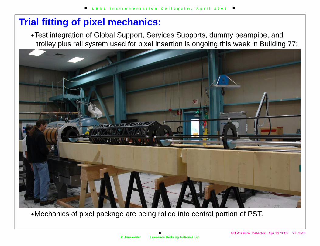
Trial fitting of pixel mechanics:•Test integration of Global Support, Services Supports, dummy
trolley plus rail system used for pixel insertion is ongoing this
•Mechanics of pixel package are being rolled into central portio

L B N L I n s t r u m e n t a t i o n C o l l o q u i m , A p r i l 2 0 0 5
TLAS Pixel Detector , Apr 13 2005 28 of 46
te by Summer 05.umping vendors.out 25% of total).t of 112 needed)
ports and global
June - Nov 05.lies) by Dec 05.
6ly 06.e ready to install into
r 07, and circulation
luminosity in the
K. Einsweiler Lawrence Berkeley National LabA
Current Status of Pixel Construction:•Wafer probing of electronics will be completed in a few days.•Off-detector electronics production is underway, will be comple•A total of about 700 bare modules have been accepted from b•About 500 pixel modules have been assembled and tested (ab•A total of 20 disk sectors (out of 48 needed) and 20 staves (ou
have been assembled and are partially or completely tested.•Most of the necessary mechanical objects, including local sup
mechanics, have been built and tested.•Services are in production or in procurement. Installation from•Expect to complete assembly of two “endcaps” (3-disk assemb•Expect to complete assembly of six barrel half-shells by Apr 0•Plan to integrate complete detector with services from May-Ju•Will carry out complete electrical testing on surface, and will b
ATLAS in Oct 06.•Current LHC schedule calls for closing machine vacuum in Ap
of single beams in July 07. •Expect short collider run in Fall 07, with potential for integrated
range from 1 pb-1 to 1fb-1

L B N L I n s t r u m e n t a t i o n C o l l o q u i m , A p r i l 2 0 0 5
TLAS Pixel Detector , Apr 13 2005 29 of 46
ules
cted charge through with error functions.
to 50MRad dose.
K. Einsweiler Lawrence Berkeley National LabA
Performance of Production Pixel ModThreshold and noise performance:
•Measure threshold and noise for each channel by stepping inje200 values, with 100 injections each. Fit resulting histograms
•Left plot is threshold, right plot is noise. Module was irradiated
L B N L I n s t r u m e n t a t i o n C o l l o q u i m , A p r i l 2 0 0 5
TLAS Pixel Detector , Apr 13 2005 30 of 46
o tune individual 3-bit, so not perfect.
r one pixel. Low rs to about 200Ke.
K. Einsweiler Lawrence Berkeley National LabA
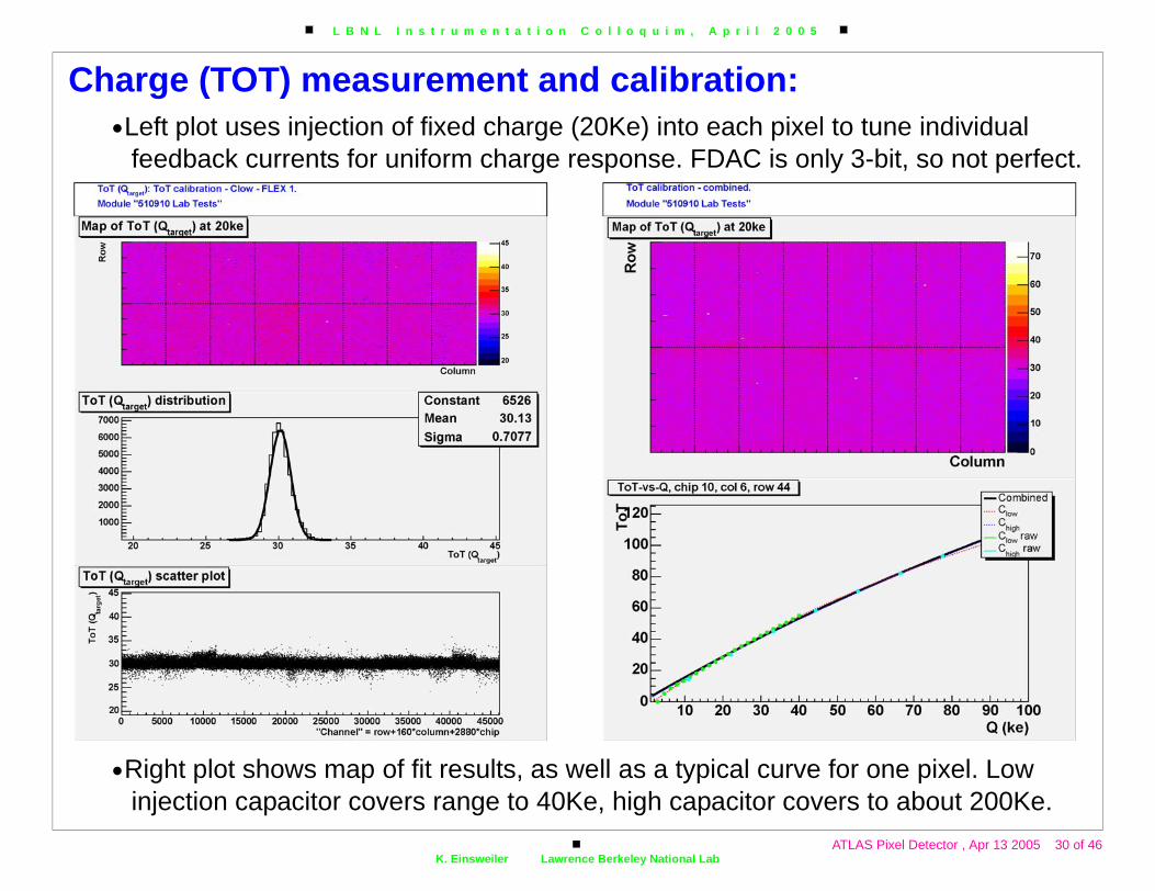
Charge (TOT) measurement and calibration:•Left plot uses injection of fixed charge (20Ke) into each pixel t
feedback currents for uniform charge response. FDAC is only
•Right plot shows map of fit results, as well as a typical curve foinjection capacitor covers range to 40Ke, high capacitor cove

L B N L I n s t r u m e n t a t i o n C o l l o q u i m , A p r i l 2 0 0 5
TLAS Pixel Detector , Apr 13 2005 31 of 46
e. Map is overdrive an 100Ke charge).
et as it would be in
K. Einsweiler Lawrence Berkeley National LabA
Measurement of timing performance:•Left plot shows timing response as a function of injected charg
(charge above threshold required to be in-time = 20ns later th
•Right plot shows result of in-time threshold scan, with timing sreal operation, and data read out only for a single crossing.

L B N L I n s t r u m e n t a t i o n C o l l o q u i m , A p r i l 2 0 0 5
TLAS Pixel Detector , Apr 13 2005 32 of 46
: source. See ur types of pixels.
plot) and the TOT k, should be at 16Ke.
K. Einsweiler Lawrence Berkeley National LabA
Self-trigger operation with Am241 X-ray source•Left plot shows hit map for self-trigger run with Am241 60KeV
shadowing by passive components on flex hybrid, and see fo
•Right plot shows average TOT distribution for one chip (middlespectrum for one pixel (lower plot), showing the Compton pea

L B N L I n s t r u m e n t a t i o n C o l l o q u i m , A p r i l 2 0 0 5
TLAS Pixel Detector , Apr 13 2005 33 of 46
current:e irradiation. In this of roughly 6nA.
t operating d pixels have 80nA.
K. Einsweiler Lawrence Berkeley National LabA
Measurement of feedback current and leakage•Left plot shows measured leakage current for each pixel befor
case, the circuit measures roughly twice the feedback current
•Right plot shows leakage current after irradiation to 50MRad, atemperature of -7C. Normal pixel has about 25nA, long-gange
L B N L I n s t r u m e n t a t i o n C o l l o q u i m , A p r i l 2 0 0 5
TLAS Pixel Detector , Apr 13 2005 34 of 46
t CERN):
protons. Able to g a one week period. three generations of odules.diation.
d at CERN SPS,
better than 5µ point dipole provided a
t several weeks, to
een trigger particle llowing, many plots ing performance.
K. Einsweiler Lawrence Berkeley National LabA
Irradiations and Stand-alone Testbeam (aIrradiations:
•Use dedicated high-intensity facility at CERN PS using 24 GeVprovide roughly 1016 p/cm2 over an area of about 2 cm2 durin
•Have used this facility over a period of three years to evaluatepixel electronics for ATLAS, both single-chips and complete m
•All electronics operated and monitored continuously during irra
Test-beam:•A large dedicated facility for ATLAS detector testing is operate
providing 180 GeV pions (and many other beams). •Pixel test setup includes dedicated strip telescope capable of
resolution projected onto pixel assemblies. A superconducting1.5T magnetic field to evaluate Lorentz angle effects.
•Have used this facility from 1997 - 2004, every year for at leasconstantly evaluate pixel prototype effort.
•Note beam is not bunched, so record the time difference betwand 40MHz clock edge used to operate pixel electronics. In foare made as a function of this ∆T measurement to explore tim

L B N L I n s t r u m e n t a t i o n C o l l o q u i m , A p r i l 2 0 0 5
TLAS Pixel Detector , Apr 13 2005 35 of 46
orithm:gle, varies from radial tracks. of the cluster of hits ge of incident angles.r of cluster. In this s of 8-9µ.
achieved with orrection”.
K. Einsweiler Lawrence Berkeley National LabA
Study position resolution versus angle and alg•Effective angle of incidence, including tilt angle and Lorentz an
about 10 degrees (pre-rad) to about 18 degrees (post-rad) for•Can use simple digital algorithm for position, where the center
is chosen. This gives a φ resolution of 12-14µ over a wide ran•Improved algorithm uses charge information to compute cente
case, get improved resolution in region relevant to radial track
•Plot is for un-irradiated modules. Similar performance can be irradiated modules, but this requires use of “digital timewalk c

L B N L I n s t r u m e n t a t i o n C o l l o q u i m , A p r i l 2 0 0 5
TLAS Pixel Detector , Apr 13 2005 36 of 46
-I1. Use track depth
00-700V.
K. Einsweiler Lawrence Berkeley National LabA
Study depletion depth for irradiated sensors:•Old measurements with first irradiated sensor studies using FE
to estimate depletion depth of the sensor:
•Observe close to full depletion (250-280µ) for bias voltage of 6

L B N L I n s t r u m e n t a t i o n C o l l o q u i m , A p r i l 2 0 0 5
TLAS Pixel Detector , Apr 13 2005 37 of 46
s:charge (most
ot area, is (average of 2%).
calibration is not that most probable
about 13-15Ke.
ttom) for 200V, s voltage.
K. Einsweiler Lawrence Berkeley National LabA
Examine charge collection in irradiated sensor•Measure charge collection uniformity and compare measured
probable) to depletion depth:
•Region with reduced charge collection, surrounding the bias dresponsible for loss in in-time efficiency for irradiated sensors
Note that absolute chargevery precise, but suggestscharge after irradiation is
Plots on left are (top to bo400V, 600V, and 700V bia

L B N L I n s t r u m e n t a t i o n C o l l o q u i m , A p r i l 2 0 0 5
TLAS Pixel Detector , Apr 13 2005 38 of 46
s with and without um:
fields. Simple model varies from about 10 arge sharing in φ.
1.4T
0.20
± 0.10 ± 0.60
± 0.50 ± 0.20
± 1.20 ± 0.50
K. Einsweiler Lawrence Berkeley National LabA
Measure Lorentz angle in sensors:•Use cluster width versus angle of incidence, doing parallel run
magnetic field, to extract angle at which cluster width is minim
•Reduction after irradiation due to reduced mobility at higher Ereproduces data well. For barrel, effective angle (Tilt-Lorentz) degrees (pre-rad) to about 18 degrees, implying significant ch
B=0
B=1.4T
θL = 9.10 ± 0.10 ± 0.60
θL = 0.20 ± 0.40
B=
θL = 3.00 ± 0.50 ±
not irradiated 9.10
dose 5 1014 n/cm2 3.00
dose 1015 n/cm2 3.20
L B N L I n s t r u m e n t a t i o n C o l l o q u i m , A p r i l 2 0 0 5
TLAS Pixel Detector , Apr 13 2005 39 of 46
odules: irradiated, in H8
7 (post-rad) modules.
g excellent e threshold plots.
ing uniform results, ave well.
K. Einsweiler Lawrence Berkeley National LabA
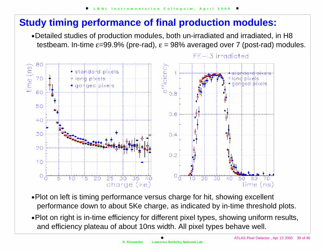
Study timing performance of final production m•Detailed studies of production modules, both un-irradiated and
testbeam. In-time ε=99.9% (pre-rad), ε = 98% averaged over
•Plot on left is timing performance versus charge for hit, showinperformance down to about 5Ke charge, as indicated by in-tim
•Plot on right is in-time efficiency for different pixel types, showand efficiency plateau of about 10ns width. All pixel types beh

L B N L I n s t r u m e n t a t i o n C o l l o q u i m , A p r i l 2 0 0 5
TLAS Pixel Detector , Apr 13 2005 40 of 46
as voltage:s voltages for 500V:
s sensor voltage,
K. Einsweiler Lawrence Berkeley National LabA
Study irradiated sensor performance versus bi•Left plot shows efficiency versus timing for different sensor bia
irradiated module. Width of timing plateau is about 8ns above
•Right plot shows in-time efficiency for irradiated module versuagain showing plateau at about 500V.

L B N L I n s t r u m e n t a t i o n C o l l o q u i m , A p r i l 2 0 0 5
TLAS Pixel Detector , Apr 13 2005 41 of 46
y:repared, in order to -layer intensity arby.e. At low intensity, e. At high intensity,
tor performance.l modules for at fourth module.
ting at high trigger the readout high intensity.
accepted) at bottom of column pairlatency)
), B-layer 0.10 - 0.15.spite the fact that afety factor of about design luminosity.
K. Einsweiler Lawrence Berkeley National LabA
Study performance of modules at high intensit•Special beam setup with lots of concrete block shielding was p
operate at maximum intensity. Just barely able to operate at B(3x10⁷/cm2/s) before triggering radiation protection alarms ne
•Study four production modules, three irradiated to lifetime dosuse strip telescope and trigger system to evaluate performancnot even small scintillators or PIN diodes were useful to moni
•All high intensity measurements were made by using four pixetracking, requiring three to provide points for track and looking
•As the off-module readout and DAQ was not capable of operarates (only several KHz), this test was really an evaluation of architecture in the front-end chip, and its capability of handling
•Various effects relevant, :* Occupancy of a pixel (time required to process hit before a new hit can be* Occupancy of column pair readout while transferring hits into EOC buffers* Length of time hits must be stored in EOC buffers before trigger decision (* Occupancy of EOC buffers themselves.
•Rate variable is column pair occupancy (#hits/colpair/crossing•Dominant effect observed to be occupancy of EOC buffers, de
there is one buffer for every 5 pixels (on average). Observe s1.5 - 2.0 over worst-case B-Layer occupancy estimate at LHC

L B N L I n s t r u m e n t a t i o n C o l l o q u i m , A p r i l 2 0 0 5
TLAS Pixel Detector , Apr 13 2005 42 of 46
t full B-layer intensity efficiency seen.
age time in EOC pancy of 0.12.
K. Einsweiler Lawrence Berkeley National LabA
•Lower left plot shows in-time efficiency for irradiated module aversus position in module at 15 degree angle. No reduction in
•Lower right plot shows in-time efficiency when latency (hit storbuffers) has been doubled. Efficiency losses seen above occu

L B N L I n s t r u m e n t a t i o n C o l l o q u i m , A p r i l 2 0 0 5
TLAS Pixel Detector , Apr 13 2005 43 of 46
LBLe of 2011-2012. This s critical to ATLAS tronics and sensors.actor 10 luminosity
st advanced mixed- May 04 via MOSIS:
2-3 years, with a first
ets of issues: rformance of t storage schemes. reement between urements for pixel amp/discriminator) -I3 design, to learn log design issues.
K. Einsweiler Lawrence Berkeley National LabA
Pixel Detector Upgrade Activities at •Expect to replace innermost pixel layer (B-layer) on a timescal
layer defines impact parameter resolution for B-tagging, and iperformance. Will concentrate on improvements in micro-elec
•Longer term CERN planning has targeted next upgrade as a fincrease to 1035, known as SLHC, perhaps in about 2015.
Upgrade R&D in Electronics and Sensors:•Designed a first test chip in IBM 0.13µ CMOS technology (mo
mode CMOS process available to us today), and submitted in
•Plan to develop improved individual building blocks over next full-scale engineering run for B-Layer upgrade in 2008.
Test chip addresses two s•First, will examine pe
different SEU-toleran•Second, will study ag
simulation and measfront-end design (prebased on present FEmore about pixel ana

L B N L I n s t r u m e n t a t i o n C o l l o q u i m , A p r i l 2 0 0 5
TLAS Pixel Detector , Apr 13 2005 44 of 46
r left):
ut, S-curve for xels in test chip.
K. Einsweiler Lawrence Berkeley National LabA
•First results from 0.13µ test chip (counterclockwise from uppe
•Preamp output versus charge, preamp and discriminator outpthreshold scan of one channel, tuned thresholds for twenty pi

L B N L I n s t r u m e n t a t i o n C o l l o q u i m , A p r i l 2 0 0 5
TLAS Pixel Detector , Apr 13 2005 45 of 46
luate performance of ronics.
silicon sensors, and rt collection length.
. Parker at Stanford type 3D sensors etry.
evices to FE-I3 nsors appear to ssing is not possible
K. Einsweiler Lawrence Berkeley National LabA
•Proceeding in collaboration with 3D sensor effort, and will evathis novel sensor concept using current production pixel elect
•3D design approach is radical departure from traditional planarhas potential to provide greater radiation hardness due to sho
First prototype run by C. Kenney and SMicrosystems Lab has produced protomatching the existing pixel FE-I3 geom
Have bump-bonded several of these dsingle chips. Unfortunately, present sesuffer from very high defect rate, so bia

L B N L I n s t r u m e n t a t i o n C o l l o q u i m , A p r i l 2 0 0 5
TLAS Pixel Detector , Apr 13 2005 46 of 46
pments more than 100
nova, Marseille, exico, Ohio,
ATLAS pixel tracker, r reflections: on tightly integrated uely good at. lus board level elopments. After e is developed.
this type seriously at tual center, and build echnical areas.d generate synergy ce already lost.at is very difficult to
ctor can help !!!bly targeted at many ary impact.
K. Einsweiler Lawrence Berkeley National LabA
Comments on LBL and Instrumentation Develo•Development and construction of ATLAS pixel detector involve
dedicated scientists and engineers from Bonn, Dortmund, GeMilano, Prague, Siegen, Udine, Wuppertal, as well as New MOklahoma, and of course LBL.
•After spending more than 10 years on the development of the with LBL playing a leading intellectual role in most areas, offe
•Development of “beyond state-of-the-art” instrumentation reliesteams of scientists and engineers, something that LBL is uniq
•Pixel electronics chain required team of several IC designers pdesigners, over 10 years, constantly following technology devworking this long on one problem, much specialized knowledg
•Major failure of LBL in this respect is to treat instrumentation ofthe highest levels in the lab, in order to create a strong intellecan atmosphere to train and retain the best people in diverse t
•We achieve sporadic success, but hard to keep momentum anacross broad areas of instrumentation. Much ATLAS experien
•Success requires a certain continuity in projects and funding thachieve in highly project-oriented DoE environment. Lab Dire
•Convinced that this type of sophisticated instrumentation, suitaother science communities at LBL/UCB can have a revolution