the biggascale emulation engine - · pdf filethe biggascale emulation engine ... the bee is a...
TRANSCRIPT
G. Wright - Berkeley Wireless Research Center 10 January 2000
1BEE
The Biggascale Emulation Engine
Gregory WrightBerkeley Wireless Research Center
G. Wright - Berkeley Wireless Research Center 10 January 2000
2BEE
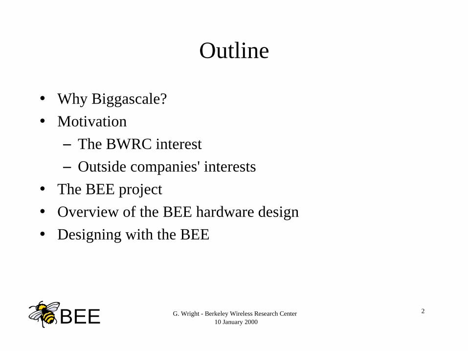
Outline
• Why Biggascale?
• Motivation
– The BWRC interest
– Outside companies' interests
• The BEE project
• Overview of the BEE hardware design
• Designing with the BEE
G. Wright - Berkeley Wireless Research Center 10 January 2000
3BEE
Why Biggascale?
Because Bigga is bigga than Giga.

G. Wright - Berkeley Wireless Research Center 10 January 2000
4BEE
Why Biggascale, Continued
The fundamental scale of the project comes from asking the question: how much computation could we do on a 1 cm square silicon chip in 0.2 um technology?
If we tile the chip with complex multiplier/accumulators, we can do about 100 billion operations per second.
The goal of the BEE project is to build an machine that can emulate, with reasonable speed, a chip that can do 100 billion operations per second.

G. Wright - Berkeley Wireless Research Center 10 January 2000
5BEE
Why Biggascale, Continued
Not quite Tera (1012), but bigga than Giga.

G. Wright - Berkeley Wireless Research Center 10 January 2000
6BEE
BEE Motivations
• From the BWRC perspective:– Build a system capable of exploring new system concepts and
algorithms for wireless communication. The focus is on gaining experience with the system level aspects of a design before committing to spinning a hard ASIC.
• From the commercial perspective:– For low volume products and those requiring frequent
reconfiguration, it would be nice to have a generic hardware platform. The BEE might be an adequate approximation of the elusive ‘software radio’.

G. Wright - Berkeley Wireless Research Center 10 January 2000
7BEE
BEE Motivation
• Some very hard problems:– BLAST radio signal processing
– Universal radio
• Some hard problems with relatively small markets:– Wireless base stations
– Scientific signal processing (e.g., Astronomy)
– Military applications (e.g., Radar and sonar)

G. Wright - Berkeley Wireless Research Center 10 January 2000
8BEE
BEE Example Application: BLAST

G. Wright - Berkeley Wireless Research Center 10 January 2000
9BEE
BEE Example Application: BLAST
• The BLAST algorithm provides extremely high spectral efficiency (26 bits s-1 Hz -1) by using each multipath ray as a separate communication channel.
• The current demonstration runs at about one-tenth of real time on four TMS32C040 DSPs. Even at this rate, we can only process a single 30 kHz channel and neglect symbol and frame synchronization. (Sync is achieved by a cable running from the transmitter to the receiver.)

G. Wright - Berkeley Wireless Research Center 10 January 2000
10BEE
BEE Example Application: BLAST
Just to run the core BLAST algorithm in real time would require about 2 x 10 9 operations per second.
To support a higher user data rate (10 Mbps instead of the current 650 kbps) would increase the processing requirements to around 30 x 10 9 operations per second.
We feel comfortable having about a factor of 3 headroom in processing power to use for all those things we haven’t yet taken into account.
G. Wright - Berkeley Wireless Research Center 10 January 2000
11BEE
The BEE Project
The BEE is a system on a chip emulator built out of field programmable gate arrays (FPGAs).
This idea isn’t new, but FPGA densities have been going up fast enough to allow us to build a system that can emulate state of the art chips.
We’re also helped by the fact that the design times for very complex chips (18 months to 2 years or even more!) Make emulation an attractive intermediate step.

G. Wright - Berkeley Wireless Research Center 10 January 2000
12BEE
The BEE Project
• What can we do with modern FPGAs?– Per chip densities are around 106 gates.
– Clock speeds are 50 to 100 MHz
– A single million gate FPGA can hold 10 to 20 complex multiplier/accumulators before becoming constrained by lack of on-chip routing resources. At a 50 MHz throughput, we can get up to about 109 multiply-accumulates per second. 100 such chips would provide us with our desired raw computing power of 100 billion operations per second. [Altera SB-4].
G. Wright - Berkeley Wireless Research Center 10 January 2000
13BEE
The BEE Project
• What can we do with modern FPGAs, continued:– Note that we’re not trying to do extensive global optimization for
the FPGA. (We’re willing, of course, to do transparent local optimizations.)
– As an example, a carefully crafted FFT using three of Xilinx’s million gate Virtex series achieved around 20 billion fixed point operations per second [Annapolis Microsystems]. A hundred chip array, running an implementation tailored to the FPGA architecture, could do nearly half a trillion operations per second.

G. Wright - Berkeley Wireless Research Center 10 January 2000
14BEE
The BEE Philosophy
Throw hardware at the problem!
We want to build a device with enough hardware resources that we can afford to waste them. This is intended to simplify the job of mapping the desired functions into the FPGAs. We specifically want to avoid ever having to split a tightly coupled function across two chips.

G. Wright - Berkeley Wireless Research Center 10 January 2000
15BEE
More Philosophy
We (well, mostly me) are leaning toward a homogeneous design.
What this means is that there probably won’t be DSP chips or microprocessors in the array. We want to stay focussed on implementing algorithms in hardware, not hardware/software partitioning and co-design.
However, we are doing some experiments to see if we would ever need DSPs embedded in the array.
G. Wright - Berkeley Wireless Research Center 10 January 2000
16BEE
The BEE Hardware
The BEE hardware will be a bunch of FPGAs, arranged in a regular array. Our preliminary specification is for 100 FPGA chips.
The array will be designed for data flow processing, typical of communication systems. This has the consequence of limiting the amount of high speed global interconnect. It also means that the BEE will NOT be a good general purpose parallel computation engine.

G. Wright - Berkeley Wireless Research Center 10 January 2000
17BEE
The BEE Hardware, Continued
Programming & maintenance I/F
uP
PE
Buffer memory
Buffer memory
Analog to
digital convertors
Digital to
analog convertors
UserI/F
RadioRX
RadioTX
RXcontrol
TXcontrol

G. Wright - Berkeley Wireless Research Center 10 January 2000
18BEE
BEE Engineering Issues
Which FPGA vendor?
We haven’t decided yet. (We are open to bribes of free or inexpensive hardware & software!)

G. Wright - Berkeley Wireless Research Center 10 January 2000
19BEE
BEE Engineering Issues
• Interconnection:– Will simply wiring the chips together be adequate, or will special
provision for long distance interconnection be required?
This is really a question about the locality of interconnection. The plan now is to possibly provide (narrow) global busses for cross-array interconnect.
Right now we’re betting that tightly coupled blocks fit within a single chip. (Keutzer asserts that tightly coupled blocks in current designs are around 50 k gates, so we’re probably OK.)
G. Wright - Berkeley Wireless Research Center 10 January 2000
20BEE
Interconnection?
New (Altera) FPGA parts can support up to 622 Mbps using an LVDS interface, although 100 Mbps is typical of the highest speed arbitrary width busses.
Most interconnect should be nearest-neighbor for data with a limited number of high speed busses for global control.
Using FPGAs for programmable interconnect is slow and robs us of needed on-chip routing resources. If we need to, we’ll use special purpose programmable interconnect chips (e.g. I-cube’s) for defining the global signal paths.

G. Wright - Berkeley Wireless Research Center 10 January 2000
21BEE
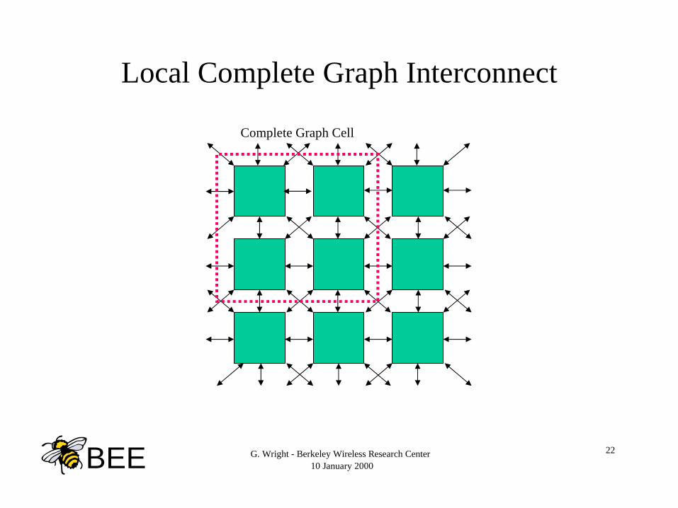
Interconnection?
• Possible FPGA interconnection architectures:– Local Complete Graph
– Local Complete Graph with busses
– Local Complete Graph with partial crossbar
– Complete crossbar
G. Wright - Berkeley Wireless Research Center 10 January 2000
22BEE
Local Complete Graph Interconnect
Complete Graph Cell
G. Wright - Berkeley Wireless Research Center 10 January 2000
23BEE
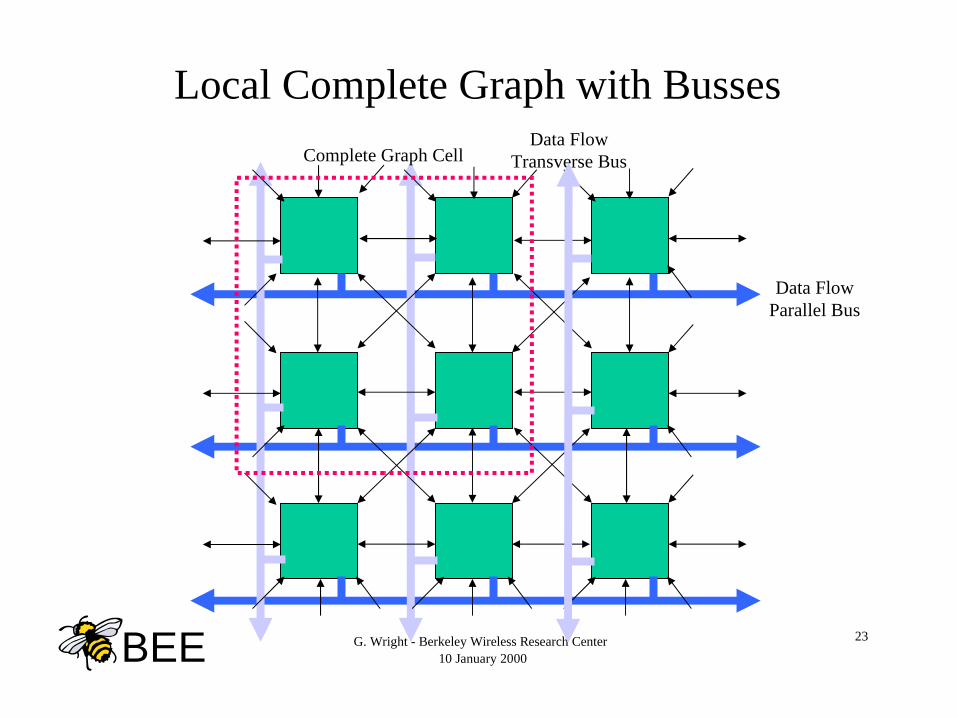
Local Complete Graph with Busses
Data FlowParallel Bus
Complete Graph CellData Flow
Transverse Bus

G. Wright - Berkeley Wireless Research Center 10 January 2000
24BEE
Local Complete Graph with Partial Crossbar
FPIC FPIC FPIC
CompleteGraph Cell
To next level interconnect

G. Wright - Berkeley Wireless Research Center 10 January 2000
25BEE
Complete Crossbar
CrossbarNetwork
G. Wright - Berkeley Wireless Research Center 10 January 2000
26BEE
BEE Engineering Issues
How are we going to get the clocks around that big array? Won’t clock skew be a disaster?
Newer devices (Xilinx’s Virtex and Altera’s Apex) have on chip DLL or PLL circuits that can be used to multiply a slower (say 25 MHz) external clock. At the lower external clock rate, skew across the array should be manageable.
The Virtex chips even provide for deskewed daisy chaining of a clock signal across an array of FPGA devices.

G. Wright - Berkeley Wireless Research Center 10 January 2000
27BEE
BEE Engineering Issues
Will the whole thing be fast enough to be useful? That depends…
…On what you consider fast enough. We can probably run algorithms intended for implementation in low power ASICs in real time. (We don’t worry about low power.)
If we use libraries of components (e.G., Multipliers, FIR filters) pre-optimized for the FPGA architecture, we will likely get a substantial fraction of custom ASIC speed.

G. Wright - Berkeley Wireless Research Center 10 January 2000
28BEE
Fast Enough?
There will be trouble if we insist on algorithms that require very fast local feedback. Getting high throughput on FPGAs usually means pipelining, which is inexpensive in lookup table based parts. For example, Altera sells a complex multiplier-accumulator that runs at 60 MHz, but has a 3 clock latency.
We will also be in big trouble if we try synthesize arbitrary HDL code and then optimize our way to speed.

G. Wright - Berkeley Wireless Research Center 10 January 2000
29BEE
BEE As a Circuit Design Tool
• We want to use the BEE to verify algorithms and system performance. This reflects a belief that the interesting optimizations in wireless systems will be at system and algorithm level.
• The BEE will get our designs to face the real wireless channel faster. Nothing ruins the day of an algorithm designer faster than confronting a real wireless channel.
• It is also important that the BEE interrupt the design flow as little as possible.
G. Wright - Berkeley Wireless Research Center 10 January 2000
30BEE
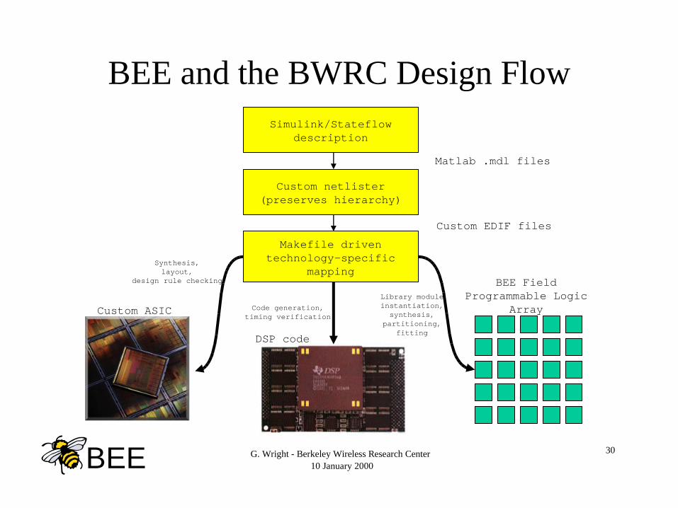
BEE and the BWRC Design FlowSimulink/Stateflow
description
Custom netlister(preserves hierarchy)
Makefile driventechnology-specific
mapping
Custom ASIC
BEE FieldProgrammable Logic
Array
DSP code
Matlab .mdl files
Custom EDIF files
Synthesis,layout,
design rule checking
Code generation,timing verification
Library moduleinstantiation,synthesis,
partitioning,fitting

G. Wright - Berkeley Wireless Research Center 10 January 2000
31BEE
BEE and the BWRC Design Flow
• The design will have to be partitioned into FPGA sized blocks. There are two approaches to this:– Automatic partitioning (available already if we adopt the Altera
Quartus software as our fitter/partitioning tool).
– Manual partitioning. In this case we add a homemade tool to the design flow after the Matlab/Simulink step, in which we partition the design and record the FPGA partitioning information in the BWRC custom netlist format.
G. Wright - Berkeley Wireless Research Center 10 January 2000
32BEE
BEE Project Status
• Initially targeted to support the universal radio project in the BWRC.
• Right now, two students and one industrial researcher working on it.
• The immediate goal is to draft specifications for what we will build. This is in cooperation with the other research groups in BWRC, who will be the end users.
• The next step is a piece of hardware to play with sometime 1Q2000.
G. Wright - Berkeley Wireless Research Center 10 January 2000
33BEE
Summary
A hardware emulation environment may be able to help us understand the algorithmic and, more importantly, the system aspects of large communication ICs.
We will be busy working on the BEE!