the blocker challenge when implementing software defined radio
TRANSCRIPT

Linköping University Post Print
The blocker challenge when implementing
software defined radio receiver RF frontends
Christer Svensson
N.B.: When citing this work, cite the original article.
The original publication is available at www.springerlink.com:
Christer Svensson, The blocker challenge when implementing software defined radio receiver
RF frontends, 2010, Analog Integrated Circuits and Signal Processing, (64), 2, 81-89.
http://dx.doi.org/10.1007/s10470-009-9446-z
Copyright: Springer Science Business Media
http://www.springerlink.com/
Postprint available at: Linköping University Electronic Press
http://urn.kb.se/resolve?urn=urn:nbn:se:liu:diva-58336

1
The Blocker Challenge when Implementing
Software Defined Radio Receiver RF
Frontends
Christer Svensson
Dept. of Electrical Engineering, Linköping University, 58183 Linköping, Sweden
+46-13281223
www.ek.isy.liu.se
Abstract— Key blocker requirements of software defined radio receivers are identified from first
principles. Three challenges are derived from these requirements, the need for passive filter banks
or tunable passive filters, a very highly linear RF front-end and a high performance analog-to-
digital converter. Each of these challenges is analyzed regarding possible solutions in the context
of state-of-the art technology.
Blockers, Integrated circuit design, Passive filters, Radio receivers.
I. Introduction
Flexible RF receiver architectures for Software or Cognitive radio’s are presently
a hot research topic [1],[2],[3],[4],[5]. Wireless systems are developing towards
more and more standards, utilizing a continuously increased number of different
frequency bands. Therefore it becomes increasingly attractive to replace today’s
multiple radio devices used for cell phones, laptops etc., with a single Software
Defined Radio (SDR) covering all bands and standards. Also, the increased
scarcity of available frequency space asks for new solutions as cognitive radio,
again requiring SDR [6]. We also see a strong military activity towards SDR [5].
A software defined radio should be able to utilize multiple frequency bands,
multiple channel bandwidths, and various channel coding using the same
hardware. A future consumer terminal should for example cover different cell
phone standards, different connectivity standards, and digital TV and radio,
calling for carrier frequencies between about 100MHz and 6GHz and bandwidths
2
from 200kHz to 20MHz. Military needs are 2MHz to 2GHz frequency range,
whereas security authorities mostly operate in the range 70MHz-400MHz.
So, why don’t we have SDR’s on the market already? The reason is simply that
there is no viable solution at hand. Considerable research effort during the last 10
years has solved many of the problems related to software radios, but
unfortunately not all. Initially, the digital processing requirements were identified
as the main obstacle. This problem is now solved through the development of
powerful application specific digital signal processors for radio baseband, see for
example [7]. Also the ADC requirement was identified as critical. This problem is
partly solved by adding ―analog preprocessing‖ to the architecture [4]. Finally,
numerous flexible electronic RF frontends have been proposed, for example
[4],[8]. So, from this perspective we may say that SDR is here and we may
identify some contemporary products as software defined radios. However, this is
not true regarding a wide frequency range. It is very doubtful that the dream of a
very agile RF frontend without passive filters can be fulfilled [1],[9],[10]. The
reason is simply that real radio environments contain disturbers (blockers) which
are too strong to be managed by active circuits. The main objective of this paper is
to identify actual blocker requirements of a software defined radio, show how
these affect the practical implementation of a radio, and identify key problems
which need to find solutions. Hopefully, this will lead to increased efforts to solve
the identified problems among radio researchers in academia and industry, so that
the ultimate goal of a fully agile SDR will be reached.
We will start with a brief analysis of the blocker requirements in a realistic radio
environment in section II. We will then discuss its consequences in terms of
dynamic range and signal voltages in section III. Section IV deals with possible
technologies for implementation of radios with these requirements. Section V,
finally, concludes the paper.
II. Blocker requirements
Any radio shares the signal transfer medium with all other radios. The dominating
means to keep a specific communication channel isolated from all other channels
is frequency division. In classical radio frequency selectivity is facilitated through
passive filters. This is very convenient as a passive filter need no power for itself
and can manage very large signal powers. The drawback is that passive filters are

3
more or less fixed in frequency, so they are not suitable for multiple frequency
radios. Therefore, in a situation where passive filter may not be available, we need
to manage the selectivity differently, and we must handle also large signal powers.
In some cases, variable gain amplifiers, or frontend attenuators, are used to
suppress large blockers [11]. However, such solutions degrade receiver sensitivity
in the presence of blockers, which we do not consider acceptable here. So, we
need to understand how large signal powers from unwanted signals, or blockers,
are around.
In the general case we may have various transmitters in the vicinity of our radio.
We categorize these blockers in three categories, a general signal background,
particular close-by transmitters, and own transmitter (eg. in full duplex frequency
multiplexed systems, FDD).
Regarding the general background radiation, there has been a number of spectrum
occupancy studies recent years, for example [12],[13]. From [12] we find that the
strongest signal observed in an urban area (Aachen) during business hours is
about -32dBm in the frequency range 20MHz to 6000MHz. In [13] the range 30-
300MHz was covered, again in an urban area (Columbus, Ohio), and the strongest
observed signals were broadcast signals at about 90MHz and 190MHz, all with a
maximum power level of about -12dBm. In both these cases the power at a
wideband, isotropic antenna was recorded. Other measurements show similar
results.
Regarding particular close-by transmitters we will make our own estimation. The
power at our antenna from a hostile transmitter, PB, depends on the transmitter
power, PT, and the distance between the transmitter and the receiver as [14]:
T
TRB P
R
GGP
22
2
16
(1)
where we have introduced the antenna gains of the receiver and the transmitter GR
and GT. is the wavelength of the carrier, given by =c/fc, where c is the velocity
of light and fc is the carrier frequency. In most practical cases we consider both
antennas isotropic and use an antenna gain of 1.6 (2dBi), valid for a simple dipole.
This is of course a very simplified view; it assumes that the receiver antenna has
full sensitivity for all carrier frequencies and it assumes free line of sight between
4
the two antennas. Still this expression gives some hint of the signal strengths. In
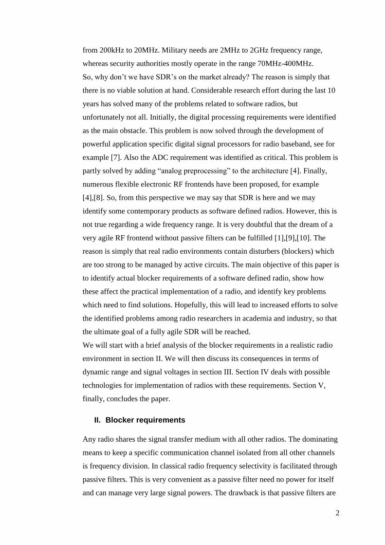
Table 1 we give some examples of realistic blockers.
TABLE 1. Overview of blocker requirements
fc, MHz R, m PT, W GT, dBi PB, dBm
VHF 70 3 10 2 25
Tetra 400 3 25 2 14
FM broadcast 90 300 50,000 -20 -2
TV broadcast 400 300 50,000 -20 -15
GSM basestation 900 30 100 -20 -29
GSM terminal 900 2 1 2 -3.5
WLAN 2400 2 1 2 -12
Let us first discuss the choice of parameters here. Regarding the first line we think
about VHF radio typically used by police, ambulance, etc. Similar transmitters are
also used by military, sometimes at higher power levels. Next line refers to the
new blue light authority radio, Tetra. For this radio a local mobile base station
may have a power of 25W. The following two columns are related to large
broadcast stations. These antennas are directed horizontally, so radiation to
ground just under the antenna is strongly attenuated. A realistic antenna gain in,
say, 45o from the horizontal plane is about -20dBi [15] and the mast height is of
the order of 300m. For a GSM base station we have a similar situation [16], but
normally a lower mast. Finally we have two terminals, a GSM terminal and a
WLAN terminal. The estimated blocker values are quite low, except for the VHF,
Tetra, FM broadcast and GSM terminal cases. VHF and Tetra are particularly
difficult, we will return to this later. Then we have the FM broadcast case. It is
also clearly seen as a strong disturber in the spectrum occupancy studies. Finally
we have the GSM terminal case, where we assume that we may have a nearby
GSM phone at 2m distance. In conclusion, if we discard the VHF and Tetra cases,
we can expect blocker levels of about 0dBm. Including VHF and Tetra indicate
values up to about 30dBm.
Coming back to the last category, our own transmitter, we experience this case for
UMTS mobile phone systems (but not for example for GSM or WiFi). In these
systems the transmitter power is about 400mW (26dBm), so we can therefore
expect a blocker power up to 26dBm (particularly if we use the same antenna).
This is thus by far the worst case for frequencies above 500MHz. We may
compare these blocker values with actual specifications for various radio
standards. For GSM a maximum out of band blocker of 0dBm is specified
5
(>80MHz from the carrier in the 1900MHz band). The same value is specified for
DCS1800. For UMTS a blocker level of -15dBm is specified. But UMTS utilizes
frequency division duplex (FDD), with a minimum frequency difference between
Tx and Rx of 135MHz (carrier around 2GHz) [3]. Tx power is normally 400mW,
thus leading to a blocker level of 26dBm. Regarding Bluetooth and WLAN, worst
case blocking power is specified to -10dBm (BT 30<fB<2000MHz, 802.11b
2500<fB<4500MHz) [17]. For the VHF bands requirements are normally higher.
In military radio for example, a blocker level of +30dBm is specified [18]. On the
other hand terrestrial TV requires only 0dBm [11]. In conclusion the specified
blocker levels for cell phone and WLAN standards are 0dBm or below, except the
FDD case, which comply with the general conclusions for carriers above about
500MHz above. For lower frequencies we have seen blocker specification of
+30dBm, which again comply with the above conclusions. See also fig. 1.
So far, we have only discussed the management of a single, strong blocker. In
practice there are many more disturber issues, related to the interaction of multiple
signals through intermodulation [1],[3]. This is however outside the scope of this
paper, which will concentrate of how to manage very strong blockers. We will
therefore not discuss the intermodulation issues further.
III. Consequences of blocker requirements
For this discussion we will consider a generic receiver architecture as in fig. 2.
The noise requirement of a radio receiver is often calculated from required
sensitivity combined with required signal to noise ratio for the actual modulation
scheme used. On the other hand we can expect that the sensitivity requirement is
originally defined from what is possible to obtain. It is therefore more reasonable
to define the noise requirement from what is attainable.
For terrestrial radio systems the lowest attainable noise level is simply the thermal
noise from ground, giving rise to an antenna noise temperature of around 300K.
We can therefore define the receiver noise requirement as about equal to the
antenna noise giving the receiver input noise spectral density:
kTSN (2)
6
Where k is Boltzmann constant and T is the antenna noise temperature. The
dynamic range of any radio receiver with channel bandwidth B and with a blocker
power of PB can then be expressed as:
kTB
PDR B (3)
This dynamic range can for example be used for calculating the ADC requirement
in the case both blocker and signal reaches the ADC. We then need to make the
full scale ADC value (peak-to-peak voltage) equal to the voltage caused by PB
over the resistance R0:
BFS PRV 08 (4)
An ADC with n bits and a sampling frequency of fs (Nyquist bandwidth fs/2) will
have a quantization noise spectral density (in voltage) of [19]:
s
nFSv
f
VS
22
12
22
2 (5)
This can be converted to power through SP=Sv2/R0. Making SP equal to the
receiver noise, SP=SN gives
kT
Pf B
s
n
3
422 (6)
where we inserted VFS from eq. (4). Note that this expression is valid for any gain
or change in impedance level between the antenna input and the ADC. So, it is
possible to estimate the ADC requirement without any knowledge of carrier
frequency, bandwidth, modulation, etc. From this definition of ADC requirement,
we can estimate the minimum ADC power consumption. In [19] it is shown that
ADC power consumption is closely related to the sampling power, PS:
B
n
sS PkTfP 32224 2 (7)
The minimum ADC power consumption is about 30 times as large as PS [19], so
let us set PADC=30PS.
Another consequence of the blocker is that we may have a large input voltage to
the receiver. The maximum peak to peak voltage over the antenna terminals can
be written:
Bpp PRV 0max 8 (8)
7
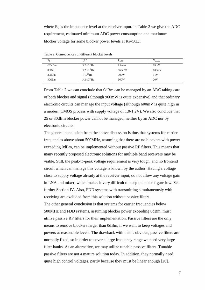
where R0 is the impedance level at the receiver input. In Table 2 we give the ADC
requirement, estimated minimum ADC power consumption and maximum
blocker voltage for some blocker power levels at R0=50.
Table 2. Consequences of different blocker levels
PB fs22n PADC Vppmax
-20dBm 3.2∙1015Hz 9.6mW 63mV
0dBm 3.2∙1017Hz 960mW 630mV
25dBm 1∙1020Hz 300W 11V
30dBm 3.2∙1020Hz 960W 20V
From Table 2 we can conclude that 0dBm can be managed by an ADC taking care
of both blocker and signal (although 960mW is quite expensive) and that ordinary
electronic circuits can manage the input voltage (although 600mV is quite high in
a modern CMOS process with supply voltage of 1.0-1.2V). We also conclude that
25 or 30dBm blocker power cannot be managed, neither by an ADC nor by
electronic circuits.
The general conclusion from the above discussion is thus that systems for carrier
frequencies above about 500MHz, assuming that there are no blockers with power
exceeding 0dBm, can be implemented without passive RF filters. This means that
many recently proposed electronic solutions for multiple band receivers may be
viable. Still, the peak-to-peak voltage requirement is very tough, and no frontend
circuit which can manage this voltage is known by the author. Having a voltage
close to supply voltage already at the receiver input, do not allow any voltage gain
in LNA and mixer, which makes it very difficult to keep the noise figure low. See
further Section IV. Also, FDD systems with transmitting simultaneously with
receiving are excluded from this solution without passive filters.
The other general conclusion is that systems for carrier frequencies below
500MHz and FDD systems, assuming blocker power exceeding 0dBm, must
utilize passive RF filters for their implementation. Passive filters are the only
means to remove blockers larger than 0dBm, if we want to keep voltages and
powers at reasonable levels. The drawback with this is obvious, passive filters are
normally fixed, so in order to cover a large frequency range we need very large
filter banks. As an alternative, we may utilize tunable passive filters. Tunable
passive filters are not a mature solution today. In addition, they normally need
quite high control voltages, partly because they must be linear enough [20].
8
Electronic solutions to the duplexer problem have been proposed in literature
[21],[22], but they can obviously not manage the high voltage, so they can only be
a complement to a duplex filter, taking care of the signal after it has been
attenuated to below 0dBm.
IV. Possible implementation techniques
The general objective with software defined radios is to have a single hardware
which covers all carrier frequencies, bandwidths and modulation formats. The
most critical issues from the implementation point of view are the maximum
blocker and the dynamic requirements. From Section III above we have concluded
that we can divide these requirements in two groups, one covering maximum
blocker levels up to 0dBm and one covering blocker levels considerably larger
than 0dBm. The first group is possibly applicable to Cell phone and WLAN
bands, excluding FDD systems, whereas the second group also includes
VHF/UHF bands.
Regarding what technology can be utilized for the implementation of these
receivers, we have further concluded that the first group possibly could live
without narrow band RF passive filters whereas the second group depends on
passive filters. The simple reason for this is that active electronics cannot handle
power levels above about 0dBm, because of the voltage level. The obvious reason
why we want to avoid passive RF filters is that they are expensive to implement.
Either we need very large banks of filters, which will be large and expensive, or
we need tunable filters, for which there are no mature technology available today.
Therefore the discussion below will be divided into systems without narrow band
passive RF filters and systems with narrow band passive RF filters. Let us start
with systems with blockers up to 0dBm, and then continue with stronger blockers.
A. Systems with blockers up to 0dBm.
We will discuss two issues in this section, input voltage limitation related to the
RF frontend and dynamic range related to the ADC.
Starting with the RF frontend, we assumed above that 0dBm might be an upper
blocker limit for electronic circuits. This was based on the fact that 0dBm gives
0.6V peak-to-peak over 50, which seems to be a reasonable voltage limit for
contemporary circuits with supply voltages of 1-1.2V. Is this true? First, would it
9
be possible to manage larger powers than 0dBm? From eq. (8) we see that we can
either reduce the impedance level or we need to manage a higher voltage (for
example by using other technologies than contemporary CMOS). In both cases
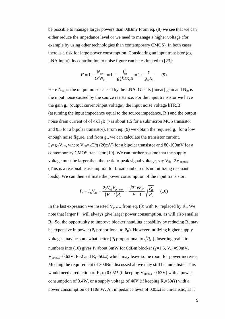
there is a risk for large power consumption. Considering an input transistor (eg.
LNA input), its contribution to noise figure can be estimated to [23]:
smsm
dn
in
out
RgBkTRg
i
NG
NF
111
2
2
2 (9)
Here Nout is the output noise caused by the LNA, G is its [linear] gain and Nin is
the input noise caused by the source resistance. For the input transistor we have
the gain gm (output current/input voltage), the input noise voltage kTRsB
(assuming the input impedance equal to the source impedance, Rs) and the output
noise drain current of of 4kTB ( is about 1.5 for a submicron MOS transistor
and 0.5 for a bipolar transistor). From eq. (9) we obtain the required gm for a low
enough noise figure, and from gm we can calculate the transistor current,
ID=gmVeff, where Veff=kT/q (26mV) for a bipolar transistor and 80-100mV for a
contemporary CMOS transistor [19]. We can further assume that the supply
voltage must be larger than the peak-to-peak signal voltage, say Vdd=2Vppmax
(This is a reasonable assumption for broadband circuits not utilizing resonant
loads). We can then estimate the power consumption of the input transistor:
s
Beff
s
ppeff
ddDIR
P
F
V
RF
VVVIP
1
32
1
2 max
(10)
In the last expression we inserted Vppmax from eq. (8) with R0 replaced by Rs. We
note that larger PB will always give larger power consumption, as will also smaller
Rs. So, the opportunity to improve blocker handling capability by reducing Rs may
be expensive in power (PI proportional to PB). However, utilizing higher supply
voltages may be somewhat better (PI proportional to BP ). Inserting realistic
numbers into (10) gives PI about 3mW for 0dBm blocker (=1.5, Veff=90mV,
Vppmax=0.63V, F=2 and Rs=50) which may leave some room for power increase.
Meeting the requirement of 30dBm discussed above may still be unrealistic. This
would need a reduction of Rs to 0.05 (if keeping Vppmax=0.63V) with a power
consumption of 3.4W, or a supply voltage of 40V (if keeping Rs=50) with a
power consumption of 110mW. An impedance level of 0.05 is unrealistic, as it
10
will give rise to very large losses. Also 3.4W is unacceptable. 40V supply voltage
is possible, but is hardly compatible with contemporary processes (unless we
choose to use a transmitter process for the receiver implementation).
Another problem with an RF frontend with very high blocker capability is that we
cannot have any voltage gain. Any voltage gain will raise the maximum peak-to-
peak voltage, which is already at its maximum (Note that automatic gain control,
etc. cannot be used as the blocker appears simultaneously with the signal). We
may possibly have power gain without voltage gain, but only if the impedance
level is reduced from stage to stage, which again leads to larger power
consumption in the following stages according to eq. (10). This means that we
cannot utilize Friis formula [23] to reduce the effect of noise figure in blocks
further into the signal path from the antenna. Instead each block must have a very
low noise figure, including the ADC. One consequence of this could be that we
should avoid using an LNA (as it does not help anyway). Still, we may need some
active circuit in the front to control the input impedance to the receiver. Generally,
we need to minimize the number of stages before the ADC, as each stage will
strongly contribute to the noise figure.
Is there any way to circumvent the power consumption problem of the input
stage[s] at high blocker level? One possibility could be to skip the LNA and use a
passive mixer directly on the antenna. Possibly the passive mixer is then
connected directly to the low noise ADC. A passive mixer does not consume
power itself, but it needs a local oscillator amplitude comparable to Vppmax. The
LO load is however mainly capacitive (transistor gates), so the high amplitude
must not necessarily lead to high power consumption.
Regarding the ADC, we calculated the ADC requirements and its power
consumption above. Utilizing the full dynamic range of the ADC will require a
minimum ADC power of about 1W, which is quite much. What can we do about
this? There are in principle two options. We can reduce the dynamic range of the
ADC by a utilizing a low-pass filter in front of it, a low-pass filter which
attenuates the strongest blockers (we assume a zero-IF architecture) [4]. Then the
requirement of the ADC is reduced and so its power consumption. This is a highly
viable solution, in principle standard in modern homodynes. It is relatively easy to
implement a steep filter at base-band, including making its bandwidth
programmable. It can for example be implemented by continuous time gm-C-
11
filters or by discrete time switched C techniques [8],[4]. The drawback with such
a filter is that it normally is active and must have a very low noise (see above), so
the power consumption may be a problem.
The other option is to add a sigma-delta loop around the ADC and run it at a very
high sampling rate [24]. The high sampling rate will reduce the need for an anti-
alias filter in front of the ADC and at the same time facilitate a large reduction in
ADC requirement due to a high oversampling ratio. A loop will give us a
further improvement of the signal to noise ratio of:
0SNR
SNRA i
i (11)
where SNRi is the signal to noise ratio for an ith
order -loop. Here A0=1 (by
definition) and
2
2
3OSRAi
(12)
4
42
5OSRA
(13)
where OSR is the oversampling ratio, OSR=fs/2B [24]. Combining (11) with (6)
(noting that the improvement in signal to noise ratio is equivalent to a
corresponding lowering of the quantization noise) gives:
i
Bs
n
AkT
Pf
1
3
422 (14)
from which we can estimate the ADC power consumption as above (eq. (7) and
the following sentence). Note that we neglect the power consumption of the
circuitry constituting the -loop, as we assume the ADC power to dominate.
Also, the ADC requirements now depend on the oversampling ratio, so we need to
consider sampling frequency and bandwidth. Below, we have used a bandwidth of
20MHz (valid for several modern radio systems as WiFi, WiMAX and LTE), and
sampling frequencies of 200 and 2000MHz. We can now recalculate the ADC
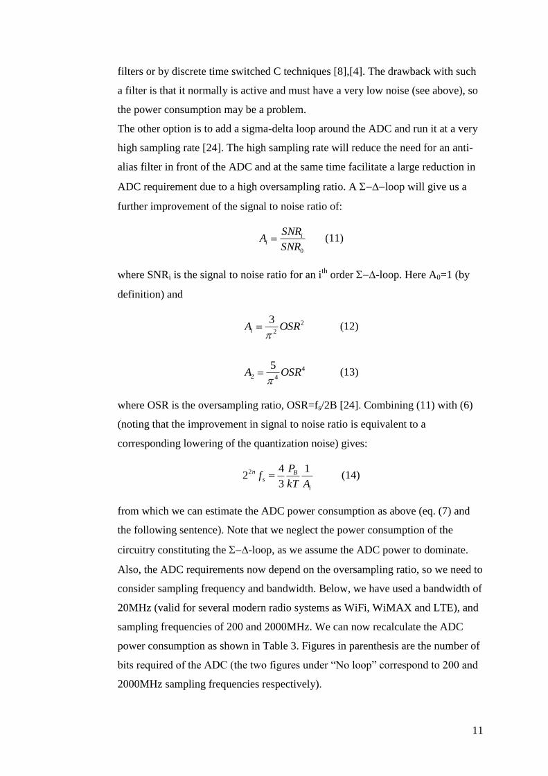
power consumption as shown in Table 3. Figures in parenthesis are the number of
bits required of the ADC (the two figures under ―No loop‖ correspond to 200 and
2000MHz sampling frequencies respectively).
12
Table 3. ADC power consumption utilizing -loops. B is assumed to 20MHz and fs to 200 or
2000MHz.
PADC for PB=0dBm PADC for PB=30dBm
No loop 960mW (15,14bit) 960W (20,19bit)
1st order, B/fs=20/200 130mW (14bit) 130W (19bit)
1st order, B/fs=20/2000 1.3mW (9bit) 1.3W (14bit)
2nd order, B/fs=20/200 30mW (13bit) 30W (18bit)
2nd order, B/fs=20/2000 3W (5bit) 3mW (9bit)
Note, that with a -loop we can reduce the ADC power consumption
considerably; with 2GHz sampling frequency it may even be possible to manage
30dBm blockers in this perspective (not necessarily in the voltage perspective).
Again, we have assumed a zero IF architecture here, so the signal into the -
loop is centered on zero frequency. Another solution is a bandpass -loop, but
then we again need to implement narrow RF filters.
From these speculations, let us move to reality. What blocker levels have been
obtained in real circuits? An interesting commercial example of a software
defined receiver is single chip TV tuners available today. One example covers 48-
960MHz range without external filters, and shows -11dBm blocker capability
during the reception of a weak signal [25] (Although it is unclear if it was
operated under minimum noise figure). In general, we may assume that a system
with a 1dB compression point (P1dBcp) of 0dBm can manage a 0dBm blocker.
Looking at reported LNAs, we found one with 4dBm compression point at very
low noise figure [26]. This narrow band base station LNA was made in a 0.25m
process with 3V supply voltage and 120mW power consumption. Another
example is an LNA with up to 4.7dBm compression point (simulated) [27].
Regarding mixers, we found a few examples of mixers with large compression
point. In [28] a 900MHz mixer with P1dBcp=-1.5dB is reported. The circuit was
implemented in a 2.7-5V bipolar process and has a minimum noise figure of
7.5dB, although it is increased with high blocker level. In [29] a 900MHz mixer in
3V, 0.8m CMOS and with 9dBm compression point and a noise figure of 28dB
is presented. A more extreme example is the X-band GaAs mixer in [30], with
9.1dBm compression point and 6.5dB noise figure.
Regarding ADCs, direct AD-conversion would require for example 15bit
resolution at 200MHz sampling frequency for the 0dBm blocker case. This is
close to ADC requirements commercially available today (One example is
LTC2209 with 16bit resolution at 160MHz sampling frequency and 1.45W power
13
consumption [31]). Utilizing -loops with high sampling frequency is also
quite possible. A second order -loop with 2GHz sampling rate, for example,
requires a 5bit ADC at 2GS/s. Such ADC’s are also available commercially, but
not at the predicted power consumption (See for example ADC082500 from
National semiconductor, with 8bit resolution at 3GS/s and 1.9W power
consumption [32]).
Several-loops have been successfully demonstrated for this application. One
example is a second order 2GS/s 1.35MHz bandwidth, 1bit quantizer -
converter aimed for CDMA receivers [33]. It was designed in 0.18m CMOS and
demonstrates 79dB SNR at a power consumption of 18mW. Its dynamic range
corresponds to a blocker power of -33dBm and a converter noise figure of 1dB.
The same dynamic range of 79dB was achieved for a 340MHz sampling rate and
20MHz bandwidth by utilizing a 4bit quantizer in [34].
B. Systems with blockers above 0dBm.
As discussed above, our judgment is that systems with blockers above 0dBm
require narrow band passive filters at their input. The issue is then which
requirements these filters should fulfill. The two most critical cases discussed in
section II are VHF blockers at 30dBm and FDD blockers at 26dBm. The Military
SDR specification for VHF states that the 30dBm blocker may occur down to 6%
frequency offset from the carrier frequency [18]. For CDMA FDD we expect a
frequency offset down to 135MHz at a carrier frequency of about 2GHz, that is an
offset of 6.75%. We therefore conclude that a receiver must manage blockers
down to 6% frequency offset from the carrier. From this we can deduce the
absolute minimum requirement of a frontend RF filter as having at least 30dB
attenuation at a frequency offset of 6%.
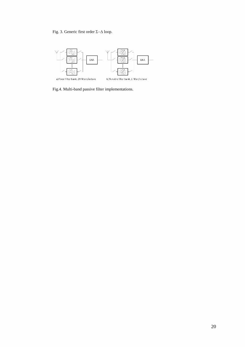
Let us first consider implementation with filter banks. It is then reasonable to
allocate half of the 6% offset to the blocker to a 30dB filter slope and half to the
pass-band. We then arrive to filters with 3% bandwidth. This then leads to the
need of 24 filters per octave. A commercial need for 100MHz to 6GHz carrier
frequency corresponding to nearly 6 octaves, will thus call for a filter bank with
144 filters. This is quite a large number, but may be feasible if each filter can be
made small enough.
14
A possible candidate for very compact filters is bulk acoustic wave filters (BAW,
FBAR), presently used commercially in mobile phones [35],[36],[37]. These
filters show very good performance, with low loss, good impedance matching,
high Q-values, good power handling and small size (~100m). There are two
possible limitations, they are less suitable below 500MHz [35] and it is not
obvious how to fabricate many filters with different frequencies at low cost. For
lower frequencies the film thickness becomes too large and fabrication of many
filters with different frequency on the same substrate will require many different
film thicknesses on this same substrate. In addition, the RF switches needed to
connect the correct filter to the RF path may introduce too much loss and
capacitance. An interesting opportunity could be to utilize induced
piezoelectricity, which can be turned off by removing a DC bias, instead of
switches [38]. So, even if BAW filters are promising for the required filter banks,
further development of this technology is needed. Another promising candidate is
MEMS resonators [39]. MEMS resonators have proven to manage frequencies
from UHF to above 1GHz, with very large Q-values, and low loss. They are small
enough (30-300m) so many can be integrated on one chip. Another benefit is
that resonators with capacitive transduction can be disconnected by removing
their DC bias, making them independent of lossy switches. There are however
also many limitations. Particularly at higher frequencies (>500MHz) the
impedance level becomes very high (k). This complicates impedance matching,
but more importantly it limits the power handling capability of the filter (because
of too high voltages according to eq. (8)) [35]. Reduction in impedance level may
be possible by using large DC bias and small gaps, but this will lead to poor
linearity and therefore also to bad power handling capability [39]. Reported high
end IIP3 for MEMS resonators is about 20dBm (at 156MHz center frequency)
[40], which is insufficient for our 30dBm P1dB requirement (using IIP3-P1dB=9.6dB
[41]).
The other alternative would be tunable filters. Assuming a bandwidth of 1% we
arrive to a minimum Q-value of the filter of about 100. Further assuming an
attenuation of 30dB for 6% offset will require a second order filter. In order to
limit the number of different filters needed, we would further require at least one
octave tuning range (limiting the number of filters in a commercial application to
6). Two promising candidates for such filters have appeared recent years;

15
electromagnetic resonator filters based on ferroelectric (or paraelectric) varactors
or mechanically controlled varactors. Electromagnetic resonator filters based on
voltage-controlled varactors based on paraelectric materials was demonstrated for
frequencies of 50-2000MHz with a tuning rage of 1.7:1 in [9]. These are made on
printed circuit boards and demonstrates insertion loss of about 3dB and an
intercept point of up to IIP3=47dBm. Assuming a ―nice‖ nonlinearity (following a
simple Taylor series) this corresponds to a compression point of about
P1dB=37dBm (using IIP3-P1dB=9.6dB [41]). Control voltages as low as 10V was
possible by applying the tuning voltage in parallel on capacitors which are serial
towards the RF voltage. Even tuning ranges exceeding one octave has been
reported [42]. Another promising technique is mechanically tuned
electromagnetic filters utilizing piezoelectric activators [43,10]. Tuning ranges
exceeding one octave (1:2.4) in the frequency range 1-5GHz has been
demonstrated. These filters have excellent properties, with insertion losses down
to 1.3dB and bandwidths down to 0.5%. They are fabricated in standard LTCC
substrates with reasonable sizes (10x20mm2) and use 100-200V actuation voltage.
The power handling capability is not reported, but is expected good, as the RF
field is completely isolated from the activator.
V. Conclusion
In a software radio perspective, assuming that the radio shall manage any
frequency within 5-10 octaves, we analyzed blocker requirements and their
consequences. We looked into three categories of blockers, general radio
background, nearby transmitters, and own transmitter (FDD case) and found that a
reasonable blocker requirement would be 30dBm for frequencies below 500MHz
and 0dBm for frequencies above 500MHz. In addition FDD systems (as UMTS)
also require nearly 30dBm.
Based on these two blocker strengths, 0dBm and 30dBm, we found that 0dBm
may be managed with active electronics, without passive filters. This will require
further technology development, as state-of-the-art technique is not sufficient.
However, our judgment is that this is possible with further development of known
techniques. We further found that 30dBm cannot be managed without passive
filters. The main argument is the high RF voltage, excluding the use of active
circuits. Analyzing the requirements of the filters we conclude that two solutions
16
are possible, either a filter bank with about 24 filters per octave or a bank of
tunable filters with a tuning range of about one octave per filter. For the filter
bank we judge that bulk acoustic wave filters appears to be the best candidate,
although the technology is not available today. For the tunable filters we judge
that electromagnetic resonators tuned either by paraelectric varactors or
electromechanically is the best candidate. Here the paraelectric capacitors appear
to be close to commercial, whereas the electromechanical solution needs some
further work.
Finally we conclude that software radio still has some way to go. One of the
toughest challenges is how to manage strong blockers; we show possible routes
how to cope with this problem. We expect that further research and development
following these routes will lead to real multi-band software defined radios. Other
challenges, not discussed in this paper, are intermodulation and multiband
transmitters. Our judgment is that these issues can be controlled by known
techniques.
Acknowledgments
The author wants to thank Profs. Jerzy Dabrowski and Spartak Gevorgian and Dr. Tim Snodgrass
for valuable discussions.
References
[1] P. B. Kenington, RF and Baseband Techniques for Software Defined Radio, Artech house,
2005.
[2] J. Mitola, ―The Software Radio Architecture‖, IEEE Communications Magazine, vol. 33, issue
5, pp. 26-38, May 1995.
[3] M. Brandolini, P. Rossi, D. Manstretta and F. Svelto, ‖Toward Multistandard Mobile
Terminals – Fully Integrated Receivers Requirements and Architectures‖, IEEE Trans. on
Microwave Theory and Techniques, vol. 53, issue 3, pp. 1026-1038, March 2005.
[4] R. Bagheri, A. Mirzaei, S. Chehrazi, M. H. Heidari, M. Lee, M. Mikhemar, W. Tang and A. A.
Abidi, ―An 800-MHz-6-GHz Software-Defined Wireless Receiver in 90-nm CMOS‖, IEEE J.
Solid-State Circuits, vol. 41, issue 12, pp. 2860-2876, December 2006.
[5] Perlman, J. Laskar and K. Lim, ―Fine-Tuning Commercial and Military Radio Design‖, IEEE
Microwave Magazine, issue 4, pp. 95-106, August 2008.
[6] Cabric, I. D, O’Donnell, M. S.-W. Chen and R. W. Brodersen, ―Spectrum Sharing Radios‖,
IEEE Circuits and Systems Magazine, second quarter 2006.

17
[7] Nilsson, E. Tell and D. Liu, ―An 11 mm2, 70 mW Fully Programmable Baseband Processor for
Mobile WiMAX and DVB-T/H in 0.12 m CMOS‖, IEEE J. Solid-State Circuits, vol 44, issue 1,
pp. 90-97, January 2009.
[8] Jakonis, K. Folkesson, J. Dabrowski, P. Eriksson and C. Svensson, ―A 2.4-GHz RF Sampling
Receiver Frontend in 0.18-m CMOS‖, IEEE Journal of Solid-State Circuits, vol. 40, issue 6, pp.
1265-1247, June 2005.
[9] M. K. Roy and J. Richter, ―Tunable Ferroelectric Filters for Software Defined Tactical
Radios‖, ISAF’06, 15th IEEE International Symposium on the Application of Ferroelectrics, pp.
348-351, August 2006.
[10] H. Joshi, H. H. Sigmarsson, D. Peroulis and W. J. Chappell, ―Highly Loaded Evanescent
Cavities for Widely Tunable High-Q Filters‖, IEEE MTT-S Int. Microwave Symposium, pp. 2133-
2136, June 2007.
[11] I. Mehr, ―Integrated TV Tuner Design for Multi-Standard Terrestrial reception‖, Proc. of the
IEEE Radio Frequency Integrated Circuits Symposium 2005, pp. 75-78, June 2005.
[12]M. Wellens, J. Wu and P. Mähönen, ―Evaluation of Spectrum Occupancy in Indoor and
Outdoor Scenario in the Context of Cognitive Radio‖, Proc. of CROWNCOM, Orlando, August
2007.
[13] S. W. Ellingson, ―Spectral Occupancy at VHF: Implications for Frequency-Agile Cognitive
Radios‖, Proc. of IEEE Vehicular Technology Conference, pp. 1379-1382, September 2005.
[14] R. Blake, Electronic Communication Systems, 2nd
ed., chapter 15, Delmar 2002.
[15] M. D. Fanton, ―Antenna Pattern and Coverage Optimization‖, ERI Technical Series
(Electronic Research Inc.), vol. 6, pp. 15-17, April 2006.
[16] C. Beckman and B. Lindmark, ―The Evolution of Base Station Antennas for Mobile
Communications‖, International Conference on Electromagnetics in Advanced Applications 2007,
pp. 85-92, September 2007.
[17] H.-K. Yoon and M. Ismail, ―A CMOS Multi-Standard Receiver Architecture for ISM and
UNII Band Applications‖, Proc. of the 2004 International Symposium on Circuits and Systems,
vol. 4, pp. IV-265-8, May 2004.
[18] T. Snodgrass, private communication.
[19] T. Sundström, B. Murmann and C. Svensson, ‖Power Dissipation Bounds for High-Speed
Nyquist Digital-to-Analog Converters‖, IEEE Trans. Circuits and Systems I, vol. 56, issue 3, pp.
509-518, March. 2009.
[20] L. Dussopt and G. M. Rebeiz, ‖Intermodulation Distortion and Power Handling in RF MEMS
Switches, Varactors, and Tunable Filters‖, IEEE Trans. on Microwave Theory and Techniques,
vol. 51, issue 4, pp. 1247-1256, April 2003.
[21] H. Darabi, ―A Blocker Filtering Technique for SAW-Less Wireless Receivers‖, IEEE Journal
of Solid-State Circuits, vol. 42, issue 12, pp. 2766-2773, December 2007.
[22] S. Kannangara and M. Faulkner, ―Adaptive Duplexer for Multiband Transceiver‖,
Proceedings Radio and Wireless Conference, 2003, pp. 381-384, August 2003.
[23] R. Blake, Electronic Communication Systems, 2nd
ed., chapter 1, Delmar 2002.

18
[24] Blad, C. Svensson, H. Johansson and S. Andersson, ‖An RF Sampling Radio Frontend Based
on -Conversion‖, 24th Norchip Conference, 2006, pp. 133-136, Nov. 2006.
[25] S. Lerstaveesin, M. Gupta, D. Kang and B.-S. Song, ‖A 48-860 MHz CMOS Low-IF Direct-
Conversion DTV Tuner‖, IEEE J. Solid-State Circuits, vol. 43, issue 9, pp. 2013-2024, September
2008.
[26] O. Boric-Lubecke, J. Lin, A. Verma, I. Lo and V. M. Lubecke, ―Multiband 0.25-m CMOS
Base Station Chips for Indirect and Direct Conversion Receivers‖, IEEE Trans. on Circuits and
Systems I, vol. 55, issue 8, pp. 2106-2115, August 2008.
[27] N. Ahsan, C. Svensson and J. Dabrowski, ―Highly Linear Wideband Low Power Current
Mode LNA‖, International Conference on Signals and Electronic Systems 2008, pp. 73-76,
September 2008.
[28] K. L. Fong, C. D. Hull and R. G. Meyer, ―A Class AB Monolithic Mixer for 900MHz
Applications‖, IEEE J. Solid-State Circuits, vol. 32, issue 8, pp. 1166-1172, August 1997.
[29] T. K.-K. Kan, K.-C. Mak, D. Ma and H. C. Luong, ‖A 2-V 900-MHz CMOS Mixer for GSM
Receivers‖, IEEE International Symposium on Circuits and Systems I, pp. I-327-I-330, May 2000.
[30] S. A. Maas, ―A GaAs MESFET Mixer with Very Low Intermodulation‖, IEEE Trans. of
Microwave Theory and Techniques, vol. MTT-35, issue 4, pp. 425-429, April 1987.
[31] http://www.linear.com/pc/productDetail.jsp?navId=H0,C1,C1155,C1001,C1150,P38869.
[32] http://webench.national.com/appinfo/adc/ghz_adc.html
[33] H. Dagher, P. A. Stubberud, W. K. Masenten, M. Conta and T. V. Dinh, ―A 2-GHz Analog-
to-Digital Delta-Sigma Modulator for CDMA Receivers With 79-dB Signal-to-Noise Ratio in
1.23-MHz Bandwidth‖, IEEE J. Solid-State Circuits, vol. 39, issue 11, pp. 1819-1827, November
2004.
[34] L. J. Breems, R. Rutten, R. H. M. van Veldhoven and G. van der Weide, ‖A 56mW
Continuous-Time Quadrature Cascaded Modulator With 77 dB DR in a Near Zero-IF 20 MHz
Band‖, IEEE J. Solid-State Circuits, vol. 42, issue 12, pp. 2696-2705, December 2007.
[35] R. Aigner, J. Ella, H.-J. Timme, L. Elbrecht, W. Nessler and S. Marksteiner, ‖Advancement
of MEMS into RF-Filter Applications‖, Digest, Int. Electron Devices Meeting 2002, pp. 897-900,
2002.
[36] R. Aigner, ―MEMS in RF-Filter Applications: This Film Acoustic-Wave Technology‖, The
13th Int. Conference on Solid-State Sensors, Actuators and Microsystems 2005, vol 1, pp. 5-8,
June 2005.
[37] Yu, W. Pang, H. Zhang and E. S. Kim, ―Ultra Temperature-Stable Bulk-Acoustic-Wave
Resonators with SiO2 Compensation Layer‖, IEEE Trans. on Ultrasonics, Ferroelectrics, and
Frequency Control, vol. 54, issue 10, pp. 2102-2109, Oct. 2007.
[38] J. Berge, A. Vorobiev, W. Steichen and S. Gevorgian, ‖Tuneably Solidly Mounted Thin Film
Bulk Acoustic Resonators Based on BaxSr1-xTiO3 Films‖, IEEE Microwave and Wireless
Components Letters, vol. 17, issue 9, pp. 655-657, Sept. 2007.
[39] C. T. C: Nguyen, ―MEMS Technology for Timing and Frequency Control‖, IEEE Trans. on
Ultrasonics, Ferroelectrics and Frequency Control‖, vol. 54, issue 2, pp. 251-270, February 2007.

19
[40] Y.-W. Lin, S.-S. Li, Z. Ren and C. T.-C. Nguyen, ‖Third-Order Intermodulation Distortion in
Capacitively-Driven VHF Micromechanical Resonators‖, Proc. IEEE Ultrasonic Symposium, pp.
1592-1595, Sept. 2005.
[41] B. Razavi, RF Microelectronics, Prentice Hall, 1998, Chapter 2.1.1.
[42] Paratek Microwave Inc., ―Thin Film Electronically Tunable Preselectors for Software Defined
Radios‖, Microwave Journal, vol. 47, pp. 138-144, October 2004.
[43] M. Al-Ahmad, R. Maenner, R. Matz and P. Russer, ―Wide Piezoelectric Tuning of LTCC
Bandpass Filters‖, IEEE MTT-S Int. Microwave Symposium Digest, vol. 4, pp. 1275-1278, June
2005.
Fig. 1. Blocker requirements from Table 1 (triangles) and a proposed blocker mask. The broken
line refers to frequency division duplex.
Fig. 2. Generic receiver architecture.
20
Fig. 3. Generic first order loop.
Fig.4. Multi-band passive filter implementations.