the challenges of correlating silicon and models in … challenges of correlating silicon and models...
TRANSCRIPT

1
The Challenges of Correlating Silicon and Models in High
Variability CMOS Processes
Rob Aitken
ARM R&D
222
©2009Rob Aitken
Outline
§ Background
§ Variability
§ Characterization
§ Library validation
§ Debug examples
§ Conclusions

333
©2009Rob Aitken
Benchmark Results
Google Scholar Citations
100
1000
10000
100000
n10 n30 n50 n100 n300
Benchmark
Cit
ati
on
s unmodified
route
benchmark
opportunity
optimal

444
©2009Rob Aitken
Physical IP is more than NAND gates
§ 15+ foundries
§ Up to 8 process generations per foundry
§ Up to 11 variants in each generation
§ 6+ memory generators
§ 900+ standard cells per library
§ 200+ I/Os
§ 10+ views per cell
§ Plus PHY, analog IP, etc.
§ 300+ libraries per year, each with thousands of individual data elements
555
©2009Rob Aitken
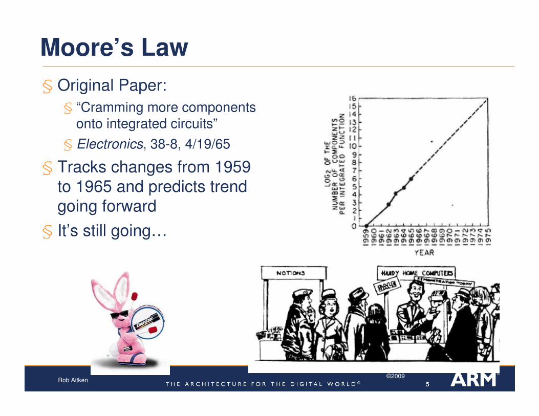
Moore’s Law
§ Original Paper:
§ “Cramming more components onto integrated circuits”
§ Electronics, 38-8, 4/19/65
§ Tracks changes from 1959
to 1965 and predicts trend going forward
§ It’s still going…
666
©2009Rob Aitken
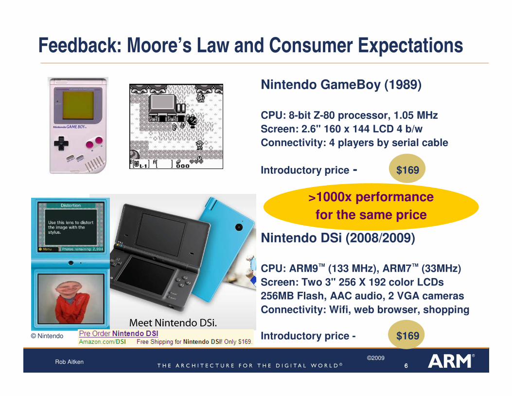
Nintendo GameBoy (1989)
CPU: 8-bit Z-80 processor, 1.05 MHz
Screen: 2.6" 160 x 144 LCD 4 b/w
Connectivity: 4 players by serial cable
Introductory price - $169
Nintendo DSi (2008/2009)
CPU: ARM9™ (133 MHz), ARM7™ (33MHz)
Screen: Two 3" 256 X 192 color LCDs
256MB Flash, AAC audio, 2 VGA cameras
Connectivity: Wifi, web browser, shopping
Introductory price - $169
>1000x performance
for the same price
Feedback: Moore’s Law and Consumer Expectations
© Nintendo
777
©2009Rob Aitken
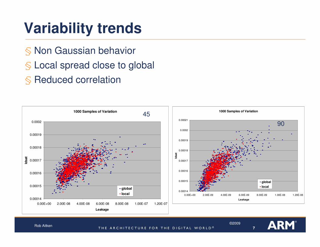
Variability trends
§ Non Gaussian behavior
§ Local spread close to global
§ Reduced correlation
1000 Samples of Variation
0.00014
0.00015
0.00016
0.00017
0.00018
0.00019
0.0002
0.00E+00 2.00E-08 4.00E-08 6.00E-08 8.00E-08 1.00E-07 1.20E-07
Leakage
Idsat
global
local
1000 Samples of Variation
0.00014
0.00015
0.00016
0.00017
0.00018
0.00019
0.0002
0.00021
0.00E+00 2.00E-09 4.00E-09 6.00E-09 8.00E-09 1.00E-08 1.20E-08
Leakage
Idsat
global
local
45
90

888
©2009Rob Aitken
Background
§ Classes of test chip:
§ ARM has multiple classes of test chip
§Library qualification chips
§Processor qualification chips
§Experimental test chips
§ Chips:
§ 2 32nm tapeouts since 9/08
§ ~40 Tapeouts in 2008, mainly first group
§ Part of shuttle or multi-project wafer
§ Usually 40-100 packaged chips
§ Challenge:
§ Silicon validation of library elements (standard cells, memory, IO)
999
©2009Rob Aitken
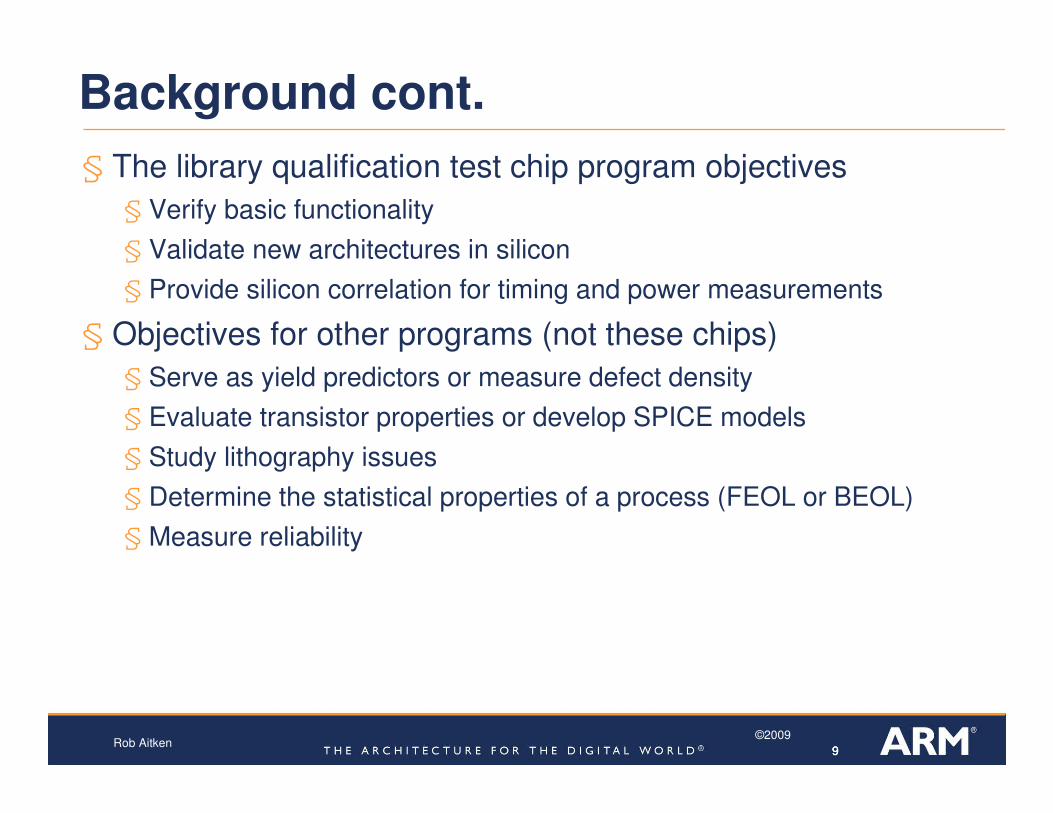
Background cont.
§ The library qualification test chip program objectives
§ Verify basic functionality
§ Validate new architectures in silicon
§ Provide silicon correlation for timing and power measurements
§ Objectives for other programs (not these chips)
§ Serve as yield predictors or measure defect density
§ Evaluate transistor properties or develop SPICE models
§ Study lithography issues
§ Determine the statistical properties of a process (FEOL or BEOL)
§Measure reliability
101010
©2009Rob Aitken
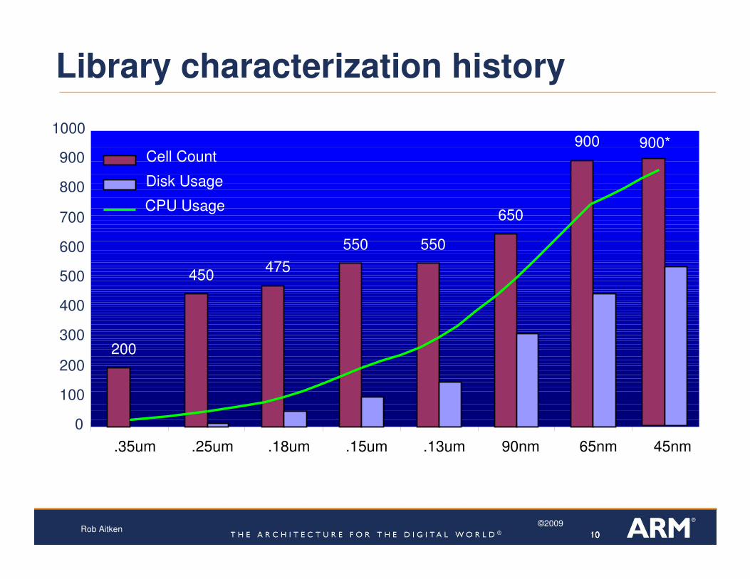
Library characterization history
200
450475
550 550
650
900
0
100
200
300
400
500
600
700
800
900
1000
.35um .25um .18um .15um .13um 90nm 65nm
Cell Count
Disk Usage
CPU Usage
900*
45nm

111111
©2009Rob Aitken
Characterization History
§ Three delay numbers: slow, typ, fast
§ Just too inaccurate
§ Linear delay: f(cap)
§What about slew rates?
§ NLDM: table f(cap, slew), interpolate between points
§Which table? How many points?
§Multiple voltage support complicated
§ Complex interconnects not modeled well
§ Current source models (CCS, ECSM)
§More complex modeling of device behavior
§ Allows for more accuracy, especially at intermediate points
§Giant files
§ Statistical models…
121212
©2009Rob Aitken
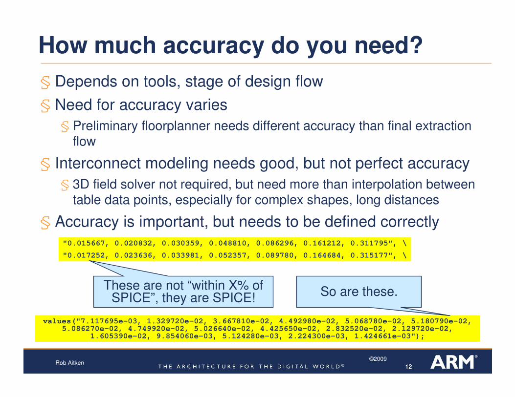
How much accuracy do you need?
§ Depends on tools, stage of design flow
§ Need for accuracy varies
§ Preliminary floorplanner needs different accuracy than final extraction flow
§ Interconnect modeling needs good, but not perfect accuracy
§ 3D field solver not required, but need more than interpolation between table data points, especially for complex shapes, long distances
§ Accuracy is important, but needs to be defined correctly"0.015667, 0.020832, 0.030359, 0.048810, 0.086296, 0.161212, 0.311795", \
"0.017252, 0.023636, 0.033981, 0.052357, 0.089780, 0.164684, 0.315177", \
These are not “within X% of SPICE”, they are SPICE!
values("7.117695e-03, 1.329720e-02, 3.667810e-02, 4.492980e-02, 5.068780e-02, 5.180790e-02, 5.086270e-02, 4.749920e-02, 5.026640e-02, 4.425650e-02, 2.832520e-02, 2.129720e-02,
1.605390e-02, 9.854060e-03, 5.124280e-03, 2.224300e-03, 1.424661e-03");
So are these.

131313
©2009Rob Aitken
§ Interpolation accuracy: 2-3%
§ Temperature, voltage variation handled with current source models
§ Variability: SS versus TT: -20% to 40%
12
34
56
7
0.032
0.048
0.08
0.14
0.264
0.512
1
0
0.05
0.1
0.15
0.2
0.25
0.3
0.35
0.4
0.45
0.5
0.55
12
34
56
7
0.032
0.048
0.08
0.14
0.264
0.512
1
0
0.05
0.1
0.15
0.2
0.25
0.3
0.35
0.4
0.45
0.5
0.55
1234567
0.032
0.048
0.08
0.14
0.264
0.512
1
0.8
0.85
0.9
0.95
1
1.05
1.1
1.15
1.2
1.25
1.3
1.35
1.4
SS
TT
Accuracy and precision:NLDM interpolation versus transistor variability

141414
©2009Rob Aitken
0.0040.0120.0280.0640.1480.344
0.0003
0.0009
0.0027
0.0083
0.0253
0.0778
0.2387
40%
60%
80%
100%
120%
140%
160%
180%
200%
perf
orm
an
ce
rati
o A
to
B
transition (scaled)
load (scaled)
1.8-2
1.6-1.8
1.4-1.6
1.2-1.4
1-1.2
0.8-1
0.6-0.8
0.4-0.6
“Scaling” of standard cell delay
§ Relative delay
for equivalent cells in two different
technologies A and B
§ Is A slower
than B or
faster?
151515
©2009Rob Aitken
Silicon Validation of Libraries
§ Basic idea
§Measure silicon, compare with model prediction
§ Things to measure
§ Delay
§ Power
§Leakage
§Dynamic
§ Challenges
§Where does silicon fit in “corners”
§Measurement accuracy
§ Single point versus table
§Model versus SPICE
§ SPICE versus silicon
§ Parametric variation
§ Presence of “soft” defects
161616
©2009Rob Aitken
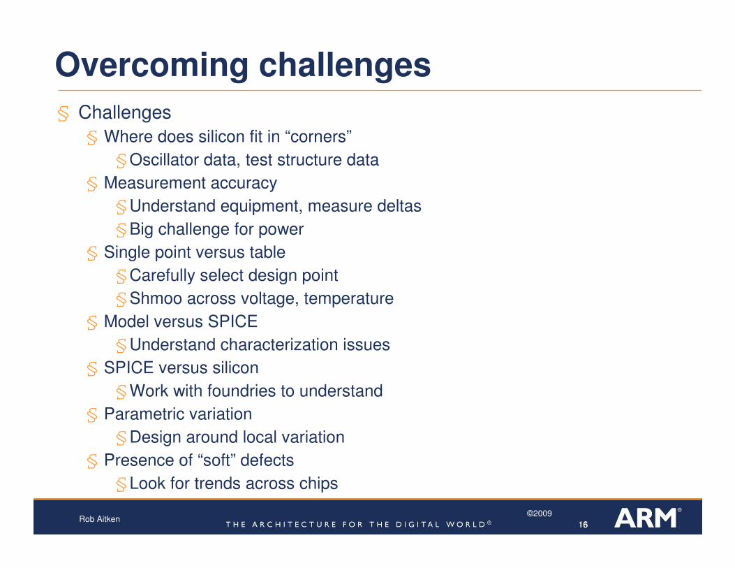
Overcoming challenges
§ Challenges
§ Where does silicon fit in “corners”
§Oscillator data, test structure data
§ Measurement accuracy
§Understand equipment, measure deltas
§Big challenge for power
§ Single point versus table
§Carefully select design point
§Shmoo across voltage, temperature
§ Model versus SPICE
§Understand characterization issues
§ SPICE versus silicon
§Work with foundries to understand
§ Parametric variation
§Design around local variation
§ Presence of “soft” defects
§Look for trends across chips
171717
©2009Rob Aitken
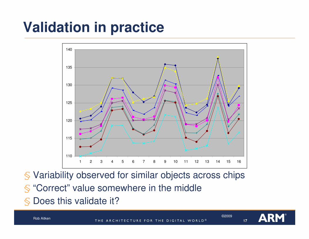
Validation in practice
§ Variability observed for similar objects across chips
§ “Correct” value somewhere in the middle
§ Does this validate it?
110
115
120
125
130
135
140
1 2 3 4 5 6 7 8 9 10 11 12 13 14 15 16
181818
©2009Rob Aitken
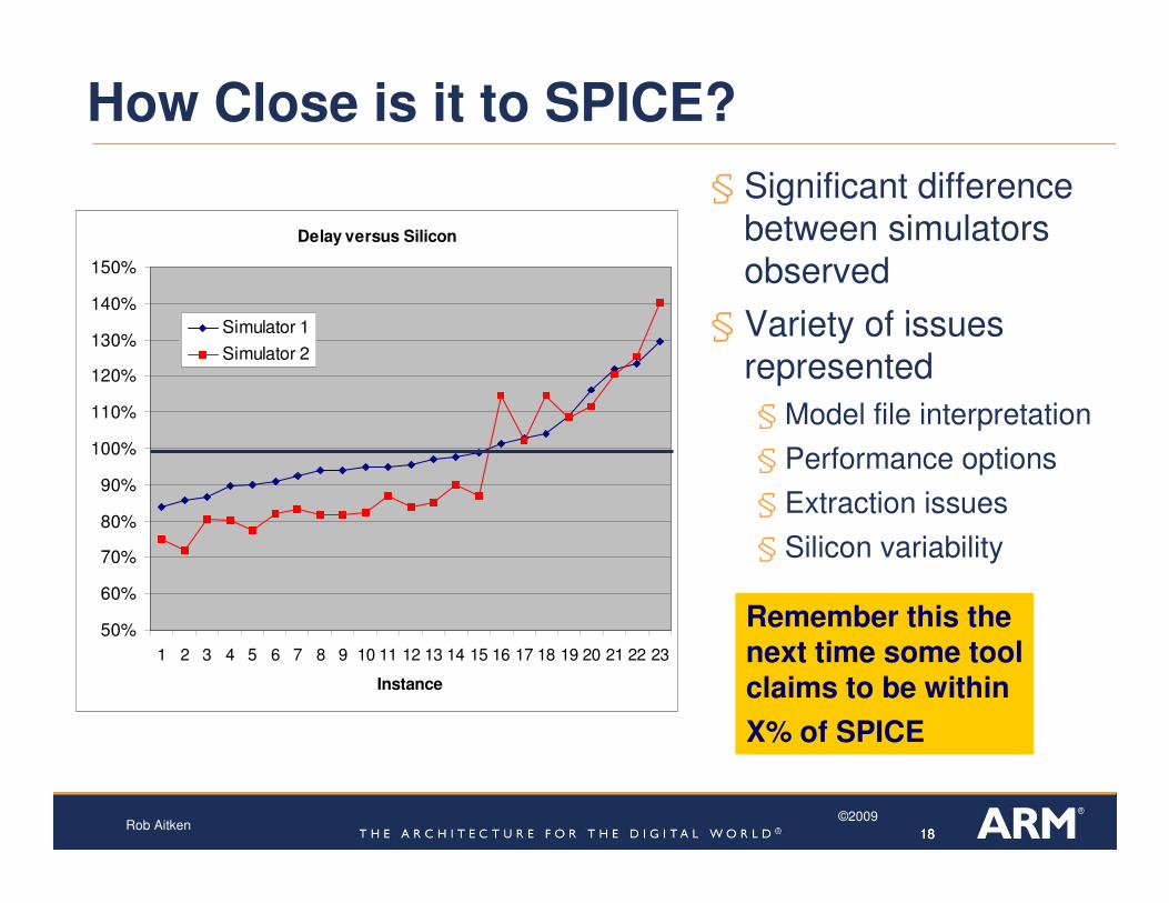
How Close is it to SPICE?
§ Significant difference between simulators
observed
§ Variety of issues represented
§Model file interpretation
§ Performance options
§ Extraction issues
§ Silicon variability
Delay versus Silicon
50%
60%
70%
80%
90%
100%
110%
120%
130%
140%
150%
1 2 3 4 5 6 7 8 9 10 11 12 13 14 15 16 17 18 19 20 21 22 23
Instance
Simulator 1
Simulator 2
Remember this thenext time some toolclaims to be within
X% of SPICE

191919
©2009Rob Aitken
Number of Contacts (Yield vs Speed)
§Typical questions after early data collection (small number of units)
§3% shift in mean but what is mean – 3σ?
Units 208/304/501 contact experiments
92%
94%
96%
98%
100%
102%
104%
106%
108%
oscila
tor_
inv_x1_cont1
1
oscila
tor_
inv_x1_cont1
2
oscila
tor_
inv_x1_cont2
1
oscila
tor_
inv_x1_cont2
2
Sta
ge D
ela
y, n
orm
alize
d

202020
©2009Rob Aitken
Min VDD for Different Design Styles
§ Question: Are any of these designs better?
§ Statistically: No
§ But: More data might give the edge to design 4
0.46
0.47
0.48
0.49
0.5
0.51
0.52
0.53
0.54
1 2 3 4 5
Instance Class
Min
VD
D
Design 1
Design 2
Design 3
Design 4

212121
©2009Rob Aitken
Variability and Validation
§ Look for correlation
§ 65nm data
§ Result: small, but measurable, distance-based effect observed
Delay Correlation vs. Circuit Distance (SEC, RVT, -40C, 1.08V, H2L)
0.955
0.96
0.965
0.97
0.975
0.98
0.985
0.99
0.995
1
1.005
0 200 400 600 800 1000 1200 1400 1600 1800 2000
Circuit block distance (um)
Co
rre
lati
on
co
eff
icie
nt

222222
©2009Rob Aitken
Sources of Variability
§ Lithography
§ Line edge roughness
§ CD variation
§ Influence of neighbors
§ Device
§Well boundary effects
§ Variation between N and P
§ Stress/strain effects
§ Interconnect
§ Dielectric variation
§ Via/contact quality
§Metal width/height variation
§ Deterministic versus Random
232323
©2009Rob Aitken
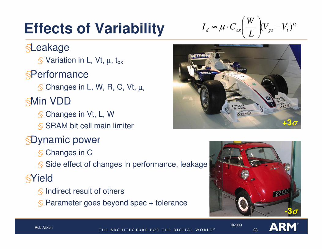
Effects of Variability
§Leakage
§ Variation in L, Vt, µ, tox
§Performance
§ Changes in L, W, R, C, Vt, µ,
§Min VDD
§ Changes in Vt, L, W
§ SRAM bit cell main limiter
§Dynamic power
§ Changes in C
§ Side effect of changes in performance, leakage
§Yield
§ Indirect result of others
§ Parameter goes beyond spec + tolerance
αµ )( tgsoxd VVL
WCI −
⋅≈
+3σσσσ
-3σσσσ

242424
©2009Rob Aitken
Local Variation Dominates in VDSM
§ Local variation (within chip) is nearly as much as global variation (between chips) at 45nm
Histogram of Leakage
0
50
100
150
200
250
0.5
1.5
2.5
3.5
4.5
5.5
6.5
7.5
8.5
9.5
10.5
local
global
Histogram of Idsat
0
20
40
60
80
100
120
140
160
1.40
E-0
41.
44E
-04
1.48
E-0
41.
52E
-04
1.56
E-0
41.
60E
-04
1.64
E-0
41.
68E
-04
1.72
E-0
41.
76E
-04
1.80
E-0
41.
84E
-04
1.88
E-0
4
local
global
1000 Monte Carlo samples, 45nm technology
252525
©2009Rob Aitken
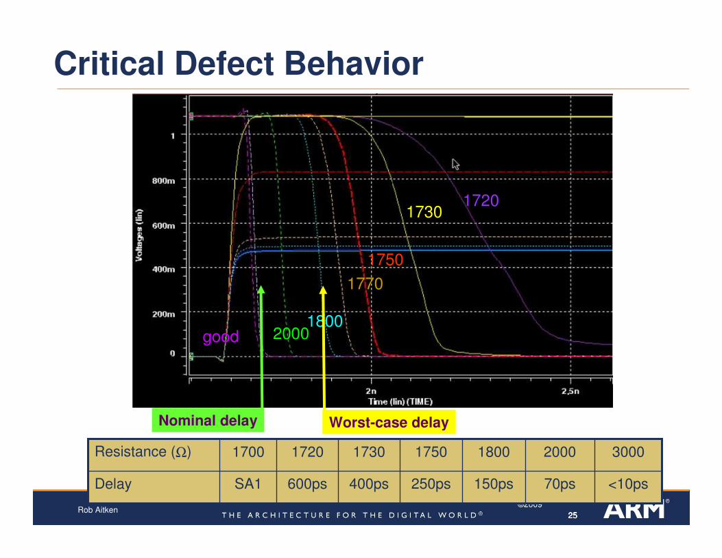
Critical Defect Behavior
17201730
1750
1770
18002000good
250ps
1750
600ps
1720
400ps
1730
<10ps70ps150psSA1Delay
3000200018001700Resistance (Ω)
Nominal delay Worst-case delay

262626
©2009Rob Aitken
Critical Variability
§ Designed for a predetermined operating point, plus margin
§ Example: SS Corner, 0.9V, 125C, 0 slack
§ Case 1: TT silicon, 0.9V, 85C
§>2X nominal delay will still function correctly
§ Case 2: SS silicon, 0.9V, 85C
§~20% extra delay will cause failure
§ Influential factors:
§Process, voltage, temperature, slack, noise
§ Expected silicon distribution: SS < 1%, TT(+/-) > 50%
§Might expect a 1-2% yield hit if SS corner just misses timing
§Guaranteed silicon distribution: None (usually)
§Could wind up with no yield 1-2% of the time (1 week per year)
§Or worse…

272727
©2009Rob Aitken
Outline
§ Background
§ Variability
§ Characterization
§ Library validation
§ Debug examples
§ Conclusions
282828
©2009Rob Aitken
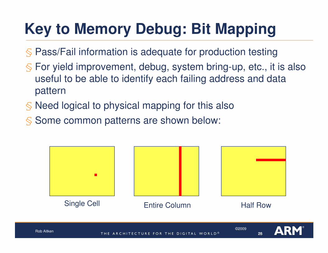
Key to Memory Debug: Bit Mapping
§ Pass/Fail information is adequate for production testing
§ For yield improvement, debug, system bring-up, etc., it is also
useful to be able to identify each failing address and data
pattern
§ Need logical to physical mapping for this also
§ Some common patterns are shown below:
Single Cell Entire Column Half Row

292929
©2009Rob Aitken
Learning From Bit Maps
Vertical Pair:
Bit Line ContactPartial Column:
Resistive Bit Line Short
Catastrophic:
Timing circuit
Multi-Row:
Address Decoder
Swath:
CMP ScratchEntire Bit:
Sense amp, I/O
303030
©2009Rob Aitken
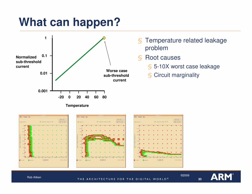
What can happen?
§ Temperature related leakage problem
§ Root causes
§ 5-10X worst case leakage
§ Circuit marginality
0.001
0.01
0.1
1
Worse case
sub-threshold
current
Normalizedsub-threshold
current
-20 0 20 40 60 80
Temperature
313131
©2009Rob Aitken
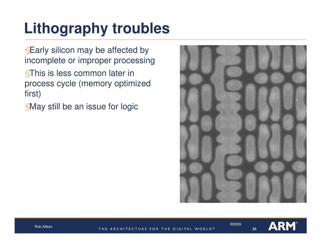
Lithography troubles
§Early silicon may be affected by
incomplete or improper processing
§This is less common later in
process cycle (memory optimized
first)
§May still be an issue for logic

323232
©2009Rob Aitken
Power Design
§ The good and the bad of power connection
§ Memory provider can only account for so much!
§ More margin = less performance
333333
©2009Rob Aitken
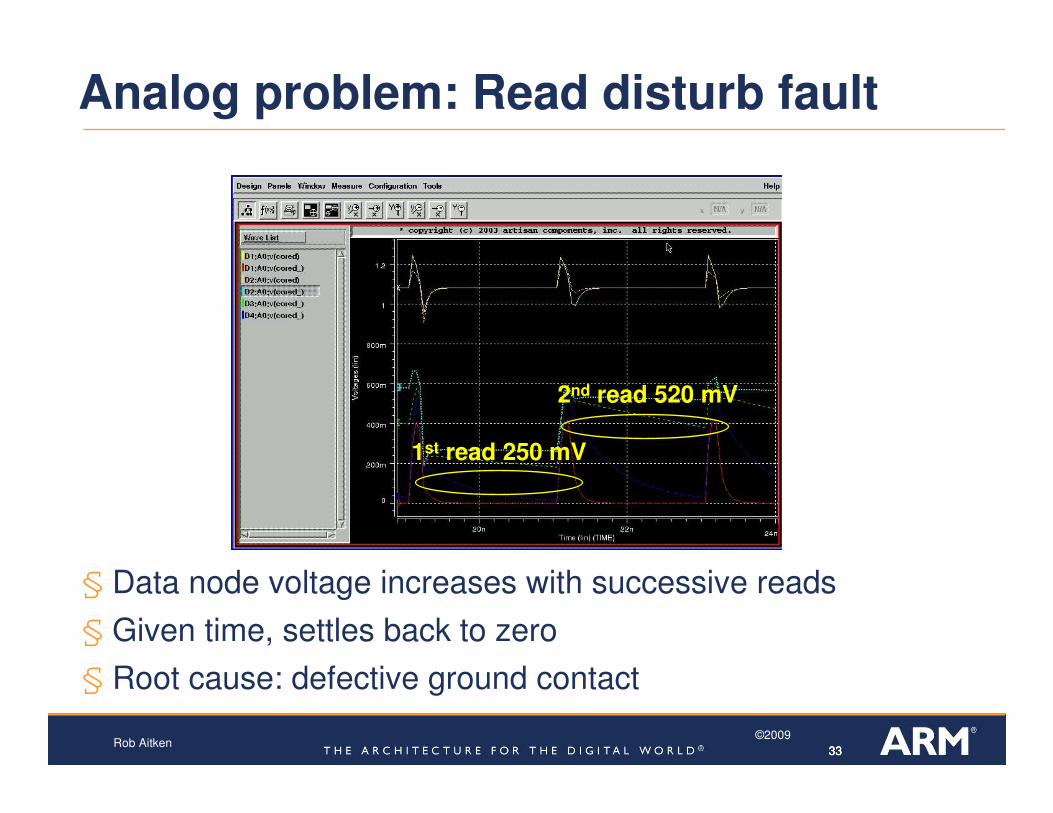
Analog problem: Read disturb fault
§ Data node voltage increases with successive reads
§ Given time, settles back to zero
§ Root cause: defective ground contact
1st read 250 mV
2nd read 520 mV
343434
©2009Rob Aitken
Conclusions
§ Validation is more complicated than you’d think
§ Variation increasingly important
§ Understanding sources of variation helps
§ An effective debug methodology helps when new troubles
arise
§Tools
§Infrastructure (silicon, equipment,
software)
§Experience
§ Feel free to send questions to [email protected]