the design of calibration circuit for analog...
TRANSCRIPT

THE DESIGN OF CALIBRATION CIRCUIT FOR ANALOG-TO-DIGITAL
CONVERTER (ADC)
By
MOHAMMAD ARIF BIN S. MOHIDEEN ALI
A Dissertation submitted for partial fulfilment of the requirement for the
degree of Master of Science (Electronic Systems Design Engineering)
March 2016

ii
ACKNOWLEDGEMENT
I would like to take this opportunity to convey my sincere and humble gratitude to those
whom have helped in making the project and thesis a success.
First and foremost, I would like to praise God for blessing me with strength and patient to
complete the project and thesis. Second, I am greatly indebted to my family and would like to
dedicate this project to them as they have supported me in many ways that I can’t easily express
in words.
Next, I am grateful to my supervisor, Mr. Zulfiqar Ali Abd Aziz for giving me the chance
to pursuit this project which I really enjoy working. He has also been of great help to me on the
project and very supportive. I honestly look at him as a role model in academic profession.
My wife and baby has been a great companion during the hard times of completing the
design and thesis.
Lastly, to my friends that I have spent considerable time with in USM that have gave
many countless advices, encouragement, and believe.

iii
TABLE OF CONTENTS
ACKNOWLEDGEMENT ii
TABLE OF CONTENTS iii
LIST OF FIGURES vi
LIST OF TABLES viii
LIST OF ABBREVIATIONS ix
LIST OF NOTATIONS AND SYMBOLS x
ABSTRACT xi
ABSTRAK xii
CHAPTER 1: INTRODUCTION 1
1.1 Background 1
1.2 Problem Statement 2
1.3 Objectives of Research 3
1.4 Scope of Research 4
1.5 Contribution of Research 5
1.6 Thesis Outline 5
CHAPTER 2: LITERATURE REVIEW 6
2.1 Introduction 6
2.2 ADC Architectures 6
2.2.1 Integrating ADC 7
iv
2.2.2 Flash ADC 9
2.2.3 Successive Approximation ADC 11
2.2.4 Delta-Sigma ADC 13
2.3 Overview of Pipelined ADC 15
2.4 Multiplying Digital-to-Analog Converter (MDAC) 16
2.5 ADC Performance Limitations 19
2.6 ADC Performance Indicators 21
2.6.1 Quantization Error 21
2.6.2 Differential Non-Linearity 23
2.6.3 Integral Non-Linearity 24
2.6.4 Signal-to-Noise Ratio (SNR) 25
2.6.5 Effective Number of Bits (ENOB) 26
2.7 Review of Calibration Techniques in Pipelined ADC 27
2.8 Summary 30
CHAPTER 3: PROPOSED DIGITAL BACKGROUND CALIBRATION CIRCUIT FOR
PIPELINED ADC 31
3.1 Introduction 31
3.2 The Pipelined Stage 32
3.3 Proposed DEC Circuit 39
3.4 Proposed Pipelined ADC 42
3.5 Proposed Calibration Circuit Type 1 44

v
3.6 Proposed Calibration Circuit Type 2 44
3.7 Summary 46
CHAPTER 4: RESULTS AND DISCUSSIONS 47
4.1 INL Measurement 47
4.2 DNL Measurement 50
CHAPTER 5: CONCLUSION AND FUTURE WORK 53
5.1 Conclusion 53
5.2 Future Work 54
REFERENCES 55
APPENDICES 59
Appendix A D Flip-Flop implementation in Verilog-A code 59
Appendix B Full-Bit Adder implementation in Verilog-A code 60
Appendix C XOR gate implementation in Verilog-A code 62

vi
LIST OF FIGURES
Page
Figure 2.1 Block diagram of a single-slope Integrating ADC (R. JACOB BAKER, 2010,
page 999). 7
Figure 2.2 Block diagram of a dual-slope Integrating ADC (R. JACOB BAKER, 2010,
page 1001). 8
Figure 2.3 Block diagram of a Flash ADC (R. JACOB BAKER, 2010, page 986) 11
Figure 2.4 Block diagram of a Successive Approximation ADC (R. JACOB BAKER, 2010,
page 1003). 12
Figure 2.5 Block diagram of a Successive Approximation ADC (R. JACOB BAKER, 2010,
page 1003). 14
Figure 2.6 Block diagram of a conventional Pipelined ADC architecture (Dave Treleaven, 2006). 15
Figure 2.7 Schematic circuit of 1.5-bit MDAC employing Switched-Capacitor (SC) (IMRAN
AHMAD, 2008). 17
Figure 2.8 Transfer curve of the 1-bit MDAC (a) in ideal case. (b) with comparator offset.
(c) with capacitor mismatch/ finite op-amp gain. (d) with charge injection
(Mingliang Liu, 2006, page 137-185). 20
Figure 2.9 Transfer curve of an ideal ADC with its corresponding quantization error (Nicholas
Gray, 2006). 22
vii
Figure 2.10 DNL plot of an ideal and actual ADC (Nicholas Gray, 2006). 24
Figure 2.11 INL plot of an ideal and actual ADC (Nicholas Gray, 2006). 25
Figure 2.12 A modified MDAC circuit with signal injection and Psuedo-random number
generator proposed by (Zhou Liren, Luo Lei, Ye Fan, Xu Jun, and Ren Junyan,
2009). 28
Figure 2.13 A pipelined ADC with calibration proposed by (Zhou Liren, Luo Lei, Ye Fan,
Xu Jun, and Ren Junyan, 2009). 28
Figure 2.14 A radix based dithering calibration proposed (Jipeng Li, and Un-Ku Moon, 2003). 30
Figure 3.1 Schematic circuit of the pipelined stage. 33
Figure 3.2 Schematic circuit of the 1.5-bit MDAC implemented in differential mode. 34
Figure 3.3 Schematic circuit of the transmission gate. 36
Figure 3.4 Schematic circuit of the op-amp used in the MDAC. 37
Figure 3.5 Input phases of the MDAC. 38
Figure 3.6 Proposed Time-Align and 4-bit Adder used in the Digital Error Correction (DEC)
circuit. 40
Figure 3.7 Proposed Digital Background Calibration circuit for 4-bit Pipelined ADC. 43
Figure 3.8 Proposed Calibration Logic Type 1 circuit. 44
Figure 3.9 Proposed Calibration Logic Type 2 circuit. 45
viii
LIST OF TABLES
Page
Table 3.1 Detail specifications of the MDAC 32
Table 4.1 INL calculation of pipelined ADC without calibration enabled. 47
Table 4.2 INL calculation of pipelined ADC with Calibration circuit type 1 enabled. 48
Table 4.3 INL calculation of pipelined ADC with Calibration circuit type 2 enabled. 49
Table 4.4 DNL calculation of Pipelined ADC without calibration enabled. 50
Table 4.5 DNL calculation of Pipelined ADC with Calibration circuit type 1 enabled. 51
Table 4.6 DNL calculation of Pipelined ADC with Calibration circuit type 2 enabled. 52

ix
LIST OF ABBREVIATIONS
ADC: Analog-to-Digital Converter
DAC: Digital-to-Analog Converter
MDAC: Multiplying Digital-to-Analog Converter
FA: Full Adder
DEC: Digital Error Correction
CMOS: Complementary metal-oxide semiconductor,
PMOS: P-type metal-oxide semiconductor
NMOS: N-type metal-oxide semiconductor
OPAMP: Operational Amplifier
MUX: Multiplexer
DFF: D Flip-Flop
INL: Integral Non-Linearity
DNL: Differential Non-Linearity
SNR: Signal-to-Noise Ratio
SINAD: Signal-to-Noise-and-Distortion Ratio
ENOB: Effective Number of Bits
PN: Pseudo-Random Number
MSB: Most Significant Bit
LSB: Least Significant Bit
GND: Ground
AGND: Analog Ground

x
LIST OF NOTATIONS AND SYMBOLS
𝑄𝑒: Quantization Error
𝑣𝐼𝑁: Analog Input
𝑉𝑆𝑇𝐸𝑃: Discrete Output
N: Number of bits
𝑉𝑑𝑑: Drain Power Supply
𝑉𝑠𝑠: Source Power Supply
𝐶𝑠: Sampling Capacitor
𝐶𝑓: Feedback Capacitor
k: Boltzmann’s Constant
T: Absolute Temperature
C: Capacitance

xi
ABSTRACT
Two types (Type 1 and Type 2) of calibration circuits for the pipelined ADC was desgined using
Verilog-A code modeling available from ahdlib Library of the Cadence Virtuoso tool. The modelling
codes were modified to suit the proposed calibration circuit. Two identical pipelined ADC blocks
(Pipelined ADC 1 and Pipelined ADC 2) were realized in 130nm Silterra CMOS process with each ADC
having a 4-bit digital output respectively. A reference voltage of 600mV was used in the operation of the
pipelined ADC with power supply connected to 1.2V for Vdd and ground GND for Vss. The pipelined
ADC operates at a sampling frequency of 2.2727MHz with input frequency from DC to 1.1364MHz. The
input range voltage of the pipelined ADC is 300mV to 900mV with common-mode voltage of 600mV.
Stages used in the construction of each pipelined ADCs employed Multiplying Digital-to-Analog
Converter (MDAC) circuit architecture. The MDAC circuit is based on the 1.5-bit switched capacitor
configuration with fully-differential operational amplifier (op-amp) gain or radix of approximately 2. A
Digital Error Correction (DEC) was also proposed using Verilog-A code modeling where two blocks,
time-align block and 4-bit adder made up the DEC block. No dithering signal or concept was used in the
proposed calibration circuit, enabling the same MDAC circuit to be used with no modifications. A DNL
of 0 LSB was achieved when calibration was enabled. The INL achieved by Calibration circuit type 1 is
from maximum +1 LSB to minimum -1 LSB. For the Calibration circuit type 2, INL achieved is
maximum +1 LSB and minimum 0 LSB. The DNL achieved by type 1 is from maximum 0 LSB to
minimum -1 LSB while type 2 achieved 0 LSB.
xii
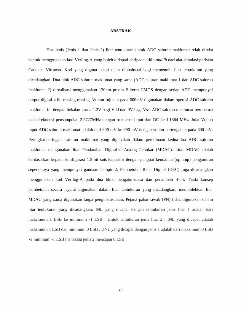
ABSTRAK
Dua jenis (Jenis 1 dan Jenis 2) litar tentukuran untuk ADC saluran maklumat telah direka
bentuk menggunakan kod Verilog-A yang boleh didapati daripada arkib ahdlib dari alat simulasi perisian
Cadence Virtuoso. Kod yang diguna pakai telah diubahsuai bagi memenuhi litar tentukuran yang
dicadangkan. Dua blok ADC saluran maklumat yang sama (ADC saluran maklumat 1 dan ADC saluran
maklumat 2) direalisasi menggunakan 130nm proses Silterra CMOS dengan setiap ADC mempunyai
output digital 4-bit masing-masing. Voltan rujukan pada 600mV digunakan dalam operasi ADC saluran
maklumat ini dengan bekalan kuasa 1.2V bagi Vdd dan 0V bagi Vss. ADC saluran maklumat beroperasi
pada frekuensi pensampelan 2.2727MHz dengan frekuensi input dari DC ke 1.1364 MHz. Julat Voltan
input ADC saluran maklumat adalah dari 300 mV ke 900 mV dengan voltan pertengahan pada 600 mV.
Peringkat-peringkat saluran maklumat yang digunakan dalam pembinaan kedua-dua ADC saluran
maklumat mengunakan litar Pendaraban Digital-ke-Analog Penukar (MDAC). Litar MDAC adalah
berdasarkan kepada konfigurasi 1.5-bit suis-kapasitor dengan penguat kendalian (op-amp) pengamiran
sepenuhnya yang mempunyai gandaan hampir 2. Pembetulan Ralat Digital (DEC) juga dicadangkan
menggunakan kod Verilog-A pada dua blok, pengatur-masa dan penambah 4-bit. Tiada konsep
pembetulan secara isyarat digunakan dalam litar tentukuran yang dicadangkan, membolehkan litar
MDAC yang sama digunakan tanpa pengubahsuaian. Pejana palsu-rawak (PN) tidak digunakan dalam
litar tentukuran yang dicadangkan. INL yang dicapai dengan tentukuran jenis litar 1 adalah dari
maksimum 1 LSB ke minimum -1 LSB . Untuk tentukuran jenis litar 2 , INL yang dicapai adalah
maksimum 1 LSB dan minimum 0 LSB . DNL yang dicapai dengan jenis 1 adalah dari maksimum 0 LSB
ke minimum -1 LSB manakala jenis 2 mencapai 0 LSB .
CHAPTER 1: INTRODUCTION
1.1 Background
Analog-to-digital converter (ADC) is commonly used in nearly all categories of electronic
systems. In the real world application, most quantities surrounding us such as voice, image, pressure,
temperature, and etc. are analog in nature. Processing such signals in its analog form by means of not
using an ADC is challenging and costly which require analog signals to be first converted into digital
signals. ADC converts the analog signals (voltages, currents) into its digital counterpart (normally
binary), which then will be used extensively by a digital signal processor (DSP). Therefore, it is clearly
known that the AD converters are indispensable parts and play important key role. This is the major
motivation of research and design of AD converters. Application of ADCs are conversion of audio signals
(mobile microphone, digital music records, etc.), conversion of video signals (cameras, frame grabber,
etc.) and value acquisition measurement (temperature, pressure, luminance, etc.). In conclusion, the
ADCs are indispensable interface between analog world and digital signal processors.

2
1.2 Problem Statement
Self-calibration in Analog-to-Digital Converters (ADC) has gain wide adaptation commonly due
to the resolution and linearity improvement it offers. Calibration techniques on ADC are commonly
categorize into two types; foreground calibration and background calibration.
In the foreground calibration, code errors at major code transitions are measured and stored
during system start-up. Such technique lacks tracking capability when temperature and voltage supply
tend to drift coupled with device aging. The background calibration instead tracks and calibrate at real
time in the background during normal operation.
Initial calibration techniques were first conceived in analog. Calibration like the ratio independent
algorithmic (P. W. Li, M. J. Chin, P. R. Gray, and R. Castello, 1984), reference updating (C. C. Shih and
P. R. Gray, 1986), capacitor mismatch averaging (B.-S. Song, M. F. Tompset, and K. R. Lakshmikumar,
1988), on-chip capacitor trimming (M. de Wit, K. S. Tan, and R. K. Hester, 1993) and gain trimming (H.
Ohara et. al., 1987) were all implemented in the analog domain. The major drawback of these analog
calibration techniques is the complexity of circuit implementation. For example, capacitor based
calibration would require the use of large array of capacitors to reduce capacitance mismatch and in gain
based calibration complex modification on the operational amplifier (op-amp) is done to reduce gain
offset. This increases the layout area tremendously of the calibration realization. Furthermore, the analog
implementation of the calibration circuit tend to lower the conversion speed of the ADC block and
complex in circuit construction (Zhou Liren, Luo Lei, Ye Fan, Xu Jun, and Ren Junyan, 2009).
The digitally controlled self-calibration (H.-S. Lee, D. A. Hodges, and P. R. Gray, 1984) and
digital-domain calibration (S.-H. Lee and B.-S. Song 1992) techniques were later proposed to alleviate the
disadvantages of the analog calibration techniques but were developed more for Successive
Approximation Register (SAR) ADC and Flash ADC, respectively.
3
In current trending, digital implementation of the calibration circuit are being researched
extensively compared to its analog counterpart. Resolution of the pipelined ADC is limited by the
accuracy of both the sub-ADC the sub-DAC being employ in each stage. Practically, pipelined ADC can
achieve 10-bit resolution accuracy with no calibration and no trimming if stringent design and layout
techniques (Cheongyuen Tsang, 2008) are practiced. However, to achieve resolution accuracy of higher
than 10-bit, trimming or calibration is commonly adopted (Cheongyuen Tsang, 2008).
Most background calibration techniques employed on the pipelined ADC tend to be complex.
Implemented in the digital domain, calibration techniques such as skip-and-fill algorithm with non-linear
interpolation, sample-and-hold queue, Least-Mean-Square (LMS) adaptive algorithm, dithering based
technique, LMS equalization method and etc. require large digital signal processing blocks. Such large
digital signal processing blocks will need to be extensively verified for correct functionality and stringent
timing requirements.
1.3 Objectives of Research
Below are the primary objectives or goals that are desired to be achieved from this research, they
are;
To implement a proposed digital background calibration circuit for pipelined ADC architecture
using Verilog-A code modeling.
To achieve improvement on INL and DNL of pipelined ADC being integrated to the proposed
digital background calibration circuit.
To proof the workability and functionality of a calibration technique implemented using Verilog-
A code modeling instead of Matlab modeling.

4
1.4 Scope of Research
Review on pipelined ADC need to be initiated to understand the working principles and
fundamental sub-blocks that make up the pipelined ADC. Non-idealities need to be reviewed to
understand its causes, sources, and mitigation steps that can be employed to reduce it. Few calibration
approaches in reducing non-idealities need to be studied.
The pre-designed pipelined stage in 130 nm Silterra CMOS process will need to be analyzed on
Cadence Virtuoso simulation tool to identify limitation towards exact specifications given and correct
operation of the stage.
A Digital Error Correction (DEC) will be built to be integrated with the pipelined ADC. The
pipelined ADC need to be constructed and validated to test the functionality of the DEC. Verilog-A code
is to be used in the modeling of DEC.
Next, Calibration circuit will be built to be integrated the pipelined ADC. The DEC block is
necessary in the functional validation of Calibration circuit. Performance verifications such as INL and
DNL will be conducted to assess the improvement brought by the Calibration circuit

5
1.5 Contribution of Research
A digital background calibration for the pipelined ADC from the mainstream is proposed. The
concept of the calibration is proofed using Verilog-A coding for rapid prototype. Verilog-A code allows
logic and analog block to be easily build and verified before venturing into real circuit design.
1.6 Thesis Outline
Chapter 2 provides a brief overview of the operation of pipelined ADC, non-linearity errors or
non-idealities in pipelined ADCs, performance indicators that involved in the measurement of non-
linearity, and general overview of available calibration techniques.
In Chapter 3, a digital background calibration scheme realized on two pipelined ADC concept is
proposed and implemented. Two types of Calibration circuit are introduced.
Chapter 4 proofs the functionality of the calibration concept through results and presents two
performance indicators.
Chapter 5 concludes the presentation of this research and provides recommendations for future
work.
6
CHAPTER 2
LITERATURE REVIEW
2.1 Introduction
In this chapter, four different topology of ADCs are discussed in section 2.2; they are Integrating
ADC, Flash ADC, Successive Approximation ADC, and Delta-Sigma ADC.
An overview on the relevant sub-blocks needed to construct a Pipelined stage and also the
pipelined ADC using the stage are introduce in section 2.3. Fundamental operation of the whole Pipelined
ADC are briefly explained.
Non-idealities such as comparator offset, finite op-amp gain, capacitor mismatch, and charge
injection which occurs on the Pipelined ADC and the reason for calibration is needed is briefed in section
2.4.
Section 2.5 discusses on few performance indicators that determines the performance of the
Pipelined ADC. Mentioned indicators are DNL, INL, SNR, and ENOB.
Finally in section 2.6, few published pipelined ADC calibration techniques and trending
background calibration techniques are analyzed to note on design tradeoffs taken to integrate calibration
circuit into their Pipelined ADC.
2.2 ADC Architectures
Commonly, types of ADC topology is decided by the application purposes. The most important
specification that decides the type of ADC topology which is suitable for the target application is the
sampling speed. Sampling speed of ADC types is divided to four categories; they are slow, medium, fast,
and oversampling. Resolution is another specification to take note when application specification is to
meet.
7
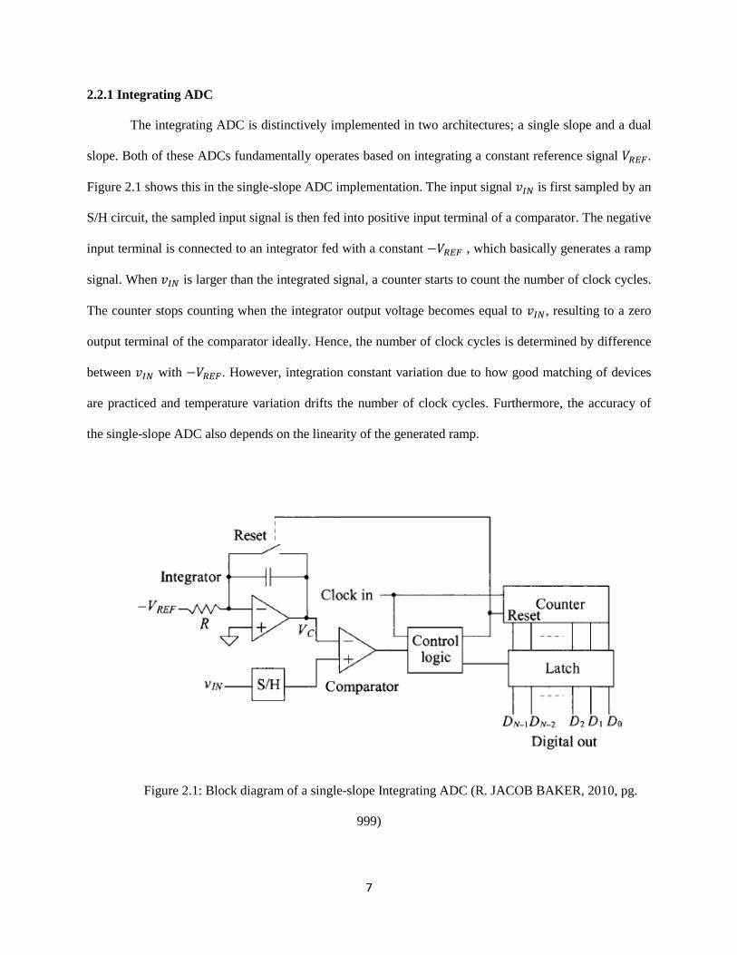
2.2.1 Integrating ADC
The integrating ADC is distinctively implemented in two architectures; a single slope and a dual
slope. Both of these ADCs fundamentally operates based on integrating a constant reference signal 𝑉𝑅𝐸𝐹.
Figure 2.1 shows this in the single-slope ADC implementation. The input signal 𝑣𝐼𝑁 is first sampled by an
S/H circuit, the sampled input signal is then fed into positive input terminal of a comparator. The negative
input terminal is connected to an integrator fed with a constant −𝑉𝑅𝐸𝐹 , which basically generates a ramp
signal. When 𝑣𝐼𝑁 is larger than the integrated signal, a counter starts to count the number of clock cycles.
The counter stops counting when the integrator output voltage becomes equal to 𝑣𝐼𝑁, resulting to a zero
output terminal of the comparator ideally. Hence, the number of clock cycles is determined by difference
between 𝑣𝐼𝑁 with −𝑉𝑅𝐸𝐹. However, integration constant variation due to how good matching of devices
are practiced and temperature variation drifts the number of clock cycles. Furthermore, the accuracy of
the single-slope ADC also depends on the linearity of the generated ramp.
Figure 2.1: Block diagram of a single-slope Integrating ADC (R. JACOB BAKER, 2010, pg.
999)
8
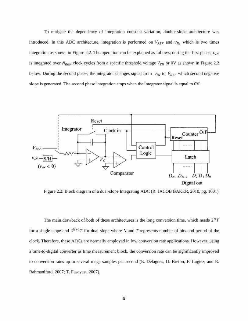
To mitigate the dependency of integration constant variation, double-slope architecture was
introduced. In this ADC architecture, integration is performed on 𝑉𝑅𝐸𝐹 and 𝑣𝐼𝑁 which is two times
integration as shown in Figure 2.2. The operation can be explained as follows; during the first phase, 𝑣𝐼𝑁
is integrated over 𝑁𝑅𝐸𝐹 clock cycles from a specific threshold voltage 𝑉𝑇𝐻 or 0V as shown in Figure 2.2
below. During the second phase, the integrator changes signal from 𝑣𝐼𝑁 to 𝑉𝑅𝐸𝐹 which second negative
slope is generated. The second phase integration stops when the integrator signal is equal to 0V.
Figure 2.2: Block diagram of a dual-slope Integrating ADC (R. JACOB BAKER, 2010, pg. 1001)
The main drawback of both of these architectures is the long conversion time, which needs 2𝑁𝑇
for a single slope and 2𝑁+1𝑇 for dual slope where N and T represents number of bits and period of the
clock. Therefore, these ADCs are normally employed in low conversion rate applications. However, using
a time-to-digital converter as time measurement block, the conversion rate can be significantly improved
to conversion rates up to several mega samples per second (E. Delagnes, D. Breton, F. Lugiez, and R.
Rahmanifard, 2007; T. Fusayasu 2007).
9
High resolution, low power consumption and small layout footprint are primarily the advantages
of these ADCs (O. Milgrome, S. Kleinfelder, and M. Levi, 1992). Such advantages allow integration of
such ADCs in the design of a CMOS image sensors proposed by (O.-B. Kwon, K.-N. Park, D.-Y. Lee,
K.-J. Lee, S.-C. Jun, C.-K. Kim, and W. Yang, 1999). Another integration is in multi-channel acquisition
systems for nuclear measurements, where architecture except the integrating ADC does not meet layout
area and power consumption expectations (E. Delagnes, D. Breton, F. Lugiez, and R. Rahmanifard, 2007;
O. Milgrome, S. Kleinfelder, and M. Levi, 1992).
2.2.2 Flash ADC
Flash converters can achieve very high sampling rates since the only fundamental building block
is a comparator. The Flash ADC consists of 2𝑁−1 parallel connected comparators with each fed with
different reference voltages as shown in Figure 2.3. Thermometer codes are generated from the
comparators when analog input signal is fed, it has 2𝑁−1 bits corresponding to each comparator and each
one show that the signal is above the corresponding reference level. A decoder is used to generate a more
convenient representation at the output. The topology allows ADC to acquire very fast conversion time.
However, flash ADCs are rarely implemented more than 8 bits (C. Lane, 1989). The main reason for this
is the exponential increase of the number of comparators as the resolution increases. The number of
comparators increases exponentially with the number of bits, so each additional bit in resolution requires
a doubling of the number of comparators. As a result, the layout size and power consumption would be
too large for higher resolutions.
10
Besides layout size and power consumption, design complexity also increase for higher
resolutions. The area increase leads to difficulties in comparator matching, and clock and signal
distribution. Furthermore, the power dissipation per unit area in an IC is limited. This means that as the
number of transistors increases, the power consumption per single transistor should be minimized. This
reduces the comparator bandwidth and analog bandwidth of the ADC as well.
Finally, the last disadvantage caused by the large number of comparators is the large input
capacitance as the large number of comparators is connected to the input signal bus. This also puts
constraints on the sample-and-hold circuit (if used) and leads to undesired bandwidth limitation. To
reduce the number of comparators, and as a result the input signal load capacitance, a number of
interpolation techniques can be used (P.-H. Chen and M. Peckerar, 2007).
Since comparator is the fundamental block, therefore its performance defines considerably
performance of the ADC. Comparator offset (R. Plassche, 2003) is one of the performance limitation that
degrades the ADC resolution. The offset can be minimized by increasing the gate size of the differential
input stage of the comparator. This, however, leads to a larger input capacitive load. Offset averaging and
auto-zeroing are alternative techniques that can be used in real time and discrete time ADCs respectively
to solve offset issue, as well as special comparator structures (M. Wang and C.-I. Chen, 2007).
Propagation delay is another important performance parameter of a comparator which can be
defined as the time taken when the analog signal has been applied to the comparator input and when a
correct decision is produced at the comparator output. This delay should be smaller than the sampling
period and failure to produce the result within the specified time can result to meta-stability, which causes
distortion of the sampled signal and makes it difficult to recover the signal again. High conversion rates
ADCs like the Flash ADC are commonly used in applications like wideband RF, optical communication,
and video decoding.

11
Figure 2.3: Block diagram of a Flash ADC (R. JACOB BAKER, 2010, pg. 986)
2.2.3 Successive Approximation ADC
The successive approximation ADC consists of a comparator, a N-bit Shift Register block, a
successive approximation register (SAR) block, and a N-bit DAC block as shown in Figure 2.4. The input
signal 𝑣𝐼𝑁 is sampled with an S/H circuit and fed into positive input terminal of the comparator. The SAR
starts the first approximation by setting the MSB to 1 with assistance of the Shift Register. This digital
combination is converted into analog representation by the DAC. The analog representation is then fed
into negative input terminal of the comparator. Comparison is performed in order to determine the MSB
value is stored, otherwise set to 0. When 𝑣𝐼𝑁 is larger than the analog representation, the MSB is stored.
As SAR consists of N-bit, the exact operation is carried out on each bit in the SAR. After determining the
last bit, the SAR generates an end of conversion (EOC) signal, and the digital representation of 𝑣𝐼𝑁 is
completed.

12
Due to the requirement of N clock cycles to perform one conversion, where N equals the number
of bits; this latency limits the conversion speed of the ADC. Besides that, having better resolution trades
off a lower conversion rate. The conversion rate can be slightly improved by converting 2 bits in one
clock cycle instead of one (K. Dabbagh-Sadeghipour, K. Hadidi, and A. Khoei, 2004). However, the
ADC resolution is limited by the resolution of DAC, offset of the comparator and quantization noise of
S/H circuit.
Significant power savings can be achieved using this type of ADC. Applications where power
constraints are stringent but sampling rates are low, the type of ADC is particularly useful for examples
sensor nodes and medical applications. With low complexity and a small number of devices, the die area
is relatively low as well.
Figure 2.4: Block diagram of a Successive Approximation ADC (R. JACOB BAKER, 2010, pg.
1003)