the development of hard x-ray nanoprobe nanoprobe...
TRANSCRIPT

Nanoprobe endstation
The Development of Hard X-ray Nanoprobe
by Montel Mirrors
Gung-Chian Yin 9/12/2014 at NSRRC 20th users’ meeting
Workshop IV

41A Soft RIXS
23A Nano-probe
25A Coherent Scattering
09A Temporally Coherent XRD
45A Submicron soft X-ray
21A Submicron XRD
24A Soft X-ray tomography
05A Protein Microrystallography
TPS
24-cell DBA
ID: 12m X 6, 7 m X 18
Plan of phase-I TPS Beamline

3
X-ray Nanoprobe at TPS
Beyond Si CMOS, Beyond Moore’s and More
Energy range:4 - 15 keV
Photon flux:1010 ~1011 photons/sec
Energy resolution:< 2×10⁻⁴ with Si(111) crystals
Beam size: ~ 40 nm at 10 keV (H × V, FWHM)
High-order harmonic contamination:≦1 × 10⁻³
Energy scanning capabilities.
Vacuum close to 10-7 torr
Adapted to 2 inch /standard Omicron holder
•Nano-electronics
•Fast speed logics
•Mass storage
•Optoelectronic
macromolecules (also
photo-voltaics)
•Energy
•Quantum computing
•Uniqueness of the research
activities

X-ray Methods
Beyond sub-ten-nm resolution (coherent)
With tens-nm resolution (incoherent)
• nano-XRF (x-ray fluorescence) – Element-specific nano-imaging
• nano-XAFS (x-ray absorption fine structures) – Local electronic structure – Local chemical environments – Element-specific, averaged over nano-area
• nano-XEOL (x-ray excited optical luminescence)
– X-ray-to-visible down-conversion efficiency in nano phosphor • nano-PXM (projection x-ray microscopy)
– Absorption and phase contrast x-ray images
• nano-CXDI (coherent x-ray diffraction imaging) • Bragg-ptychography
– strain dynamics in nano-devices
Other than X-rays
•SEM (SE, EDS, CL with high resolution) •Fly scanning •Nanomotors (optional) •Sample environment (optional)
XNP at TPS
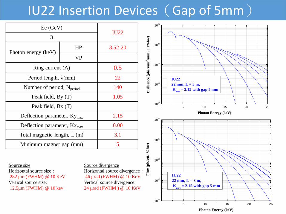
Ee (GeV) IU22
3
Photon energy (keV) HP 3.52-20
VP
Ring current (A) 0.5
Period length, λ(mm) 22
Number of period, Nperiod 140
Peak field, By (T) 1.05
Peak field, Bx (T)
Deflection parameter, Kymax 2.15
Deflection parameter, Kxmax 0.00
Total magnetic length, L (m) 3.1
Minimum magnet gap (mm) 5
0 5 10 15 20 2510
17
1018
1019
1020
1021
IU22
22 mm, L = 3 m,
Kmax
= 2.15 with gap 5 mm
Bril
lian
ce (
ph
s/s/
mr2
/mm
2/0
.1%
bw
)
Photon Energy (keV)
0 5 10 15 20 2510
12
1013
1014
1015
1016
IU22
22 mm, L = 3 m,
Kmax
= 2.15 with gap 5 mm
Flu
x (
ph
/s/0
.1%
bw
)
Photon Energy (keV)
IU22 Insertion Devices(Gap of 5mm)
Source size
Horizontal source size :
282 μm (FWHM) @ 10 KeV
Vertical source size:
12.5μm (FWHM) @ 10 kev
Source divergence
Horizontal source divergence :
46 μrad (FWHM) @ 10 KeV
Vertical source divergence:
24 μrad (FWHM ) @ 10 KeV
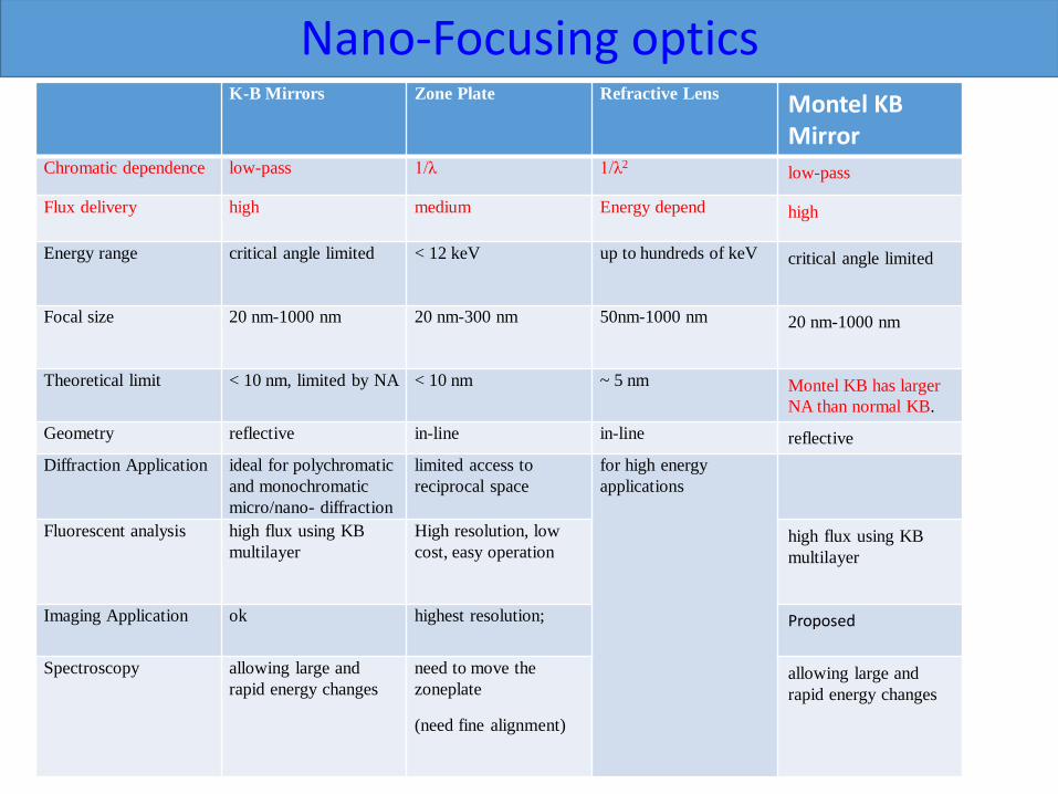
Nano-Focusing optics K-B Mirrors Zone Plate Refractive Lens Montel KB
Mirror Chromatic dependence low-pass 1/λ 1/λ2 low-pass
Flux delivery high medium Energy depend high
Energy range critical angle limited < 12 keV up to hundreds of keV critical angle limited
Focal size 20 nm-1000 nm 20 nm-300 nm 50nm-1000 nm 20 nm-1000 nm
Theoretical limit < 10 nm, limited by NA < 10 nm ~ 5 nm Montel KB has larger
NA than normal KB.
Geometry reflective in-line in-line reflective
Diffraction Application ideal for polychromatic
and monochromatic
micro/nano- diffraction
limited access to
reciprocal space
for high energy
applications
Fluorescent analysis high flux using KB
multilayer
High resolution, low
cost, easy operation high flux using KB
multilayer
Imaging Application ok highest resolution; Proposed
Spectroscopy allowing large and
rapid energy changes
need to move the
zoneplate
(need fine alignment)
allowing large and
rapid energy changes

1. Focus beam 2. Only one mirror reflection
3. No cross
Illustration of the Montel KB Mirror
3
2 Vm only
2 Hm only
1

Focus length = 11 cm
Mirror length = 11 cm
Slope error < 0.05 μrad
Objective distance is 69 m
Incident angle =4 mrad
With Rh coating
Montel optics (nested KB)
Minimum radius
for this mirror: 20 m

40nm
5.656 mrad
4.0 mrad
Simulation of Focus Spot & divergence Simulation at 10 keV, average reflection=0.802, by ray tracing
Effective Source size 12.5 μm x 12.5 μm
Source divergence 6μrad x 6μrad
FHWM 32nm x 32nm,
Simulated
Focus spot size
Simulated
Divergence

Montel Mirrors holder/aligner
Axis name Travel Range
Resolution
(minimum
movement)
Stability
1 X 10 mm 0.1um 10 nm*
2 Y 24 mm 0.1um 1um
3 Z 10 mm 0.1um 10 nm*
4 Pitch 40 mrad 0.01 urad 0.1urad*
5 Roll 40 mrad 0.1 urad 0.1urad*
6 Yaw 40 mard 0.01 urad 0.1urad*
7 Top-Y 1mm 1 um 1um
8 Top-Z 1mm 1 um 10 nm*
9 Top-Pitch (X) 1mrad 0.05 urad 0.1urad*
10 Top-Roll (Y) 1mrad 1 urad 0.1urad*
Top-4 axis (for Alignment of Montel Mirror)
Bottom-6 axis (for total mirror set)
* Holder design has not finished yet-

Prototype of the Montel Mirrors
September 2013 at JTEC
Substrate of prototype of 7cm Montel mirrors.

12
283 μm (FWHM)
Optical Scheme of KB mirror focusing
L4 = 69 m
object
Horizontal direction
s h
0.5l/ s v
L1 = 27 m
L2 = 33 m
s h
HFM1
L5 =0.11 m
d=6.25 μm
6 μrad/90μrad
261μm
12.5μm × 110/ 69000 = 20.0nm
~12.5μm (FWHM) object
Vertical direction
Double Crystal Monochromator
s v 0.5l/ s v
L1 = 69 m
6 μrad/24μrad
L2 =0.11 m
261μm 12.5μm × 110 / 69000 = 20.0nm
Demagnification Ratio:
627
Demagnification Ratio:
Stage 1: 4.5
Stage 2: -0.5
(re-define the source)
Stage 3: 627
L3 = 66 m
Slit3

Beamline 2-stage focusing
Horizontal DCM
Short in length ( <70 m )
Windowless
Vertically coherent
Montel optics
Ultimate focal spot ~ 30-40 nm
photon flux 1010-1011/sec
Shih-Hung Chang

From user’s requirements
Targeting pressure: <10-6 torr
Temp. : 10k~ 873k (Red not implement low temperature yet)
Sample Size: 1cm2~ “2” wafer
Spot Size:<40nm
Sample perpetration: Heater ~873K
(degas/decap)
Use with 2” portable sample transfer

Conceptual layout for the X-ray nanoprobe
IU22
Focusing Optics
Bragg-Ptychography
/Diffraction
SEM
Fluorescence
SS1
Preparation Chamber
Projection CCD
XEOL
Laser interferometer

The current design of the endstation 1. KB mirror 2. Sample Stage 3. Laser interferometer 4. XEOL 5. SEM 6. XRF(EDS) 7. Sample Preparation system 8. Portable sample transfer 9. Projection CCD 10. Diffraction detector 11. (system is in vacuum)
1
2
3
4 5
6
7
8
9
10
xray

Design of mirror holder and sample stage
Montel KB mirror XFR
Flexure stage,XYZ
3 axis-Rotation stage
SEM
Piezo-stage, XYZ
Laser interferometer
Beam direction
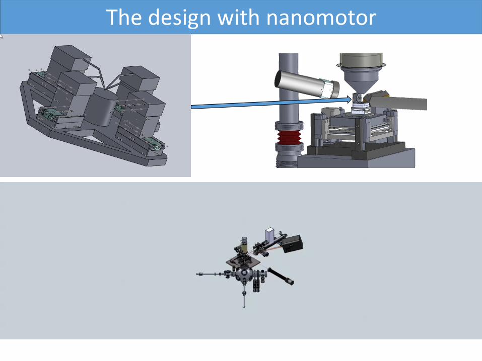
The design with nanomotor

The consideration of Preparation Chamber
Portable chamber To transfer from MBE system
Switch to standard sample holder Heating stage, Surface clean, Ion gun, e gun.
To main Chamber
Switch from 2-inch To standard omicron holder
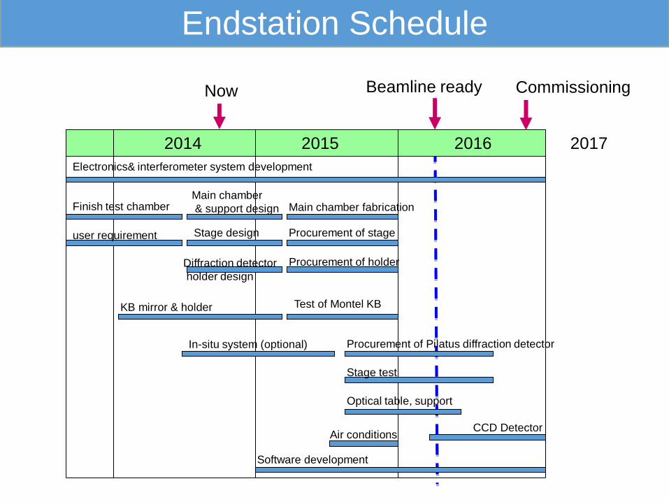
Endstation Schedule
Beamline ready
2014 2015 2016 2017
Finish test chamber Main chamber
& support design
user requirement
KB mirror & holder
Main chamber fabrication
Stage design
CCD Detector
Optical table, support
Procurement of stage
Stage test
Air conditions
In-situ system (optional)
Test of Montel KB
Procurement of Pilatus diffraction detector
Software development
Electronics& interferometer system development
Diffraction detector
holder design
Procurement of holder
Now Commissioning

Project Leader: Prof. J. Raynien Kwo (郭瑞年教授)
Construction Team
Leader
Mau-Tsu Tang (湯茂竹)
Beamline-
Shih-Hung Chang (張世汯)and Beamline Group
Endstation-
Gung-Chian Yin*,(殷廣鈐) optical design and overall system integration.
Bo-Yi Chen(陳伯毅) Mechanical engineer.
Chian-Yao Lee, (李建佑) Electronic engineer.
Huang-Yeh Chen (陳皇曄) Mechanical design and exeperiment.
Shao-Chin Tseng (曾紹欽) Sample preparation, experiment design.
Bi-Shuan Lin (林碧軒) Experiment design, XEOL, diffraction.
Shao-Yun Wu (吳紹筠) Experiment design, Diffraction
Construction Team

Progress of Testing Chamber
Vacuum:
After baking <10-7 torr
Operation at low 10-6 torr
SEM:
x100,000 (OK)
EDS:
Vortex me4 test (OK)
Interferometer: test OK
Temperature control:+- 0.02 C

Test Chamber
SEM
Turbo pump
SE Vortex ME4 detector
Granite base for
sample and mirror stages
Hi-Wedge mount
Cast iron frame
for chamber
Testing Chamber in progress

Flexure stage
Y Axis
Z Axis
SEM
EDS
SE
Turbo Pump
Laser Interferometer
Laser Path & Sample Stage
In details

Testing of integrated SEM
x10000
x50,000 x100,000
x31
Thank you for your attention !!!

The MBE system from user
Advanced Nano Epitaxy Lab, ITRI
Portable UHV
chamber for
transfer 2”wafers
in 3x10⁻¹⁰ torr for
X-ray and STM
analysis
Standard 2’’ wafer
Transported by
portable chamber

Consideration of diffraction Diffraction: By S2D2 method: Most of the Bragg angle Position can be found at 10 keV.
70 deg
45 deg
Si (5.431 Å )
Gamma delta
(002) 26.392 0
(004) 54.333 0
(202) 27.955 26.35
(204) 57.750
26.186
(224)
62.03 36.992
gamma
delta
J.Appl.Crystl(1995)28,318

29
List of Detectors
Type of experiment Detector Possible Brand
Fluorescence Multi-elements detectors (SDD/ Maia)
Vortex me4.
XEOL Spectrum Princeton instrument /Andor
•CDI/Bragg-ptychography CCD / photon counting area detector
Pilatus3 1M
Projection Microscope CCD Princeton instrument XO series
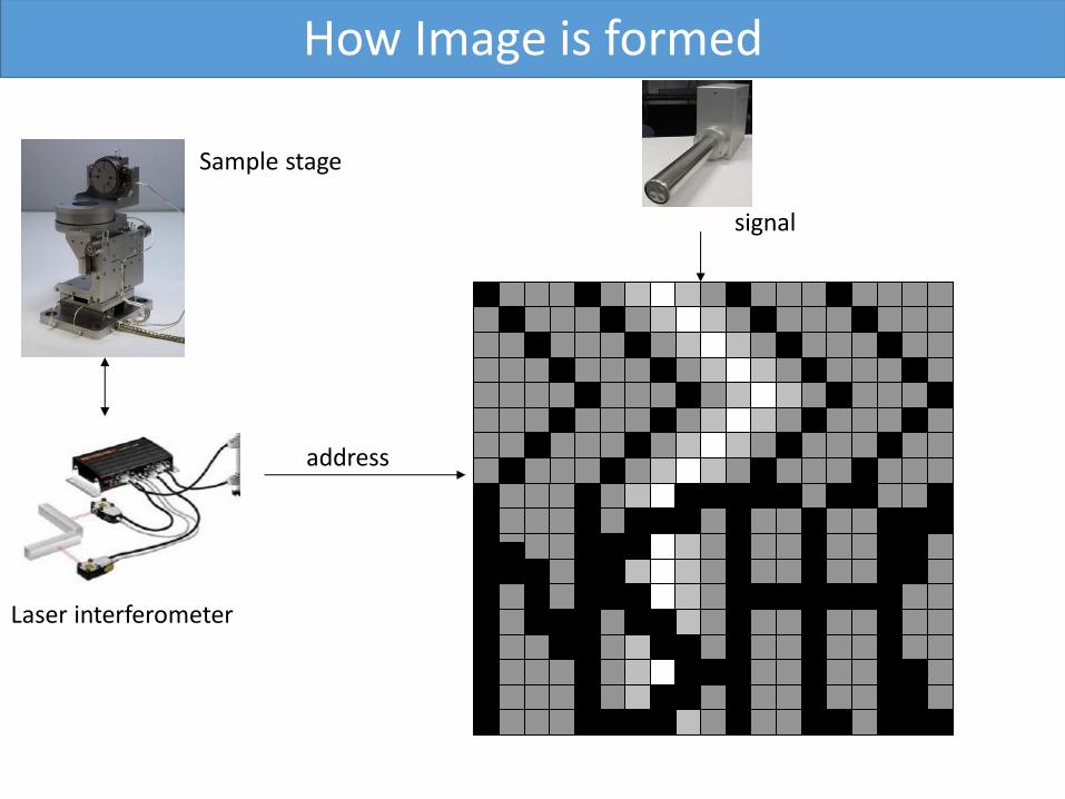
How Image is formed
Laser interferometer
Sample stage
address
signal

EDS/readout circuit test
Customize IO
Mercury-4
Customize IO test – 4k MCA @Ag
• Vortex Me4 is tested, and customized circuit is designed and tested. The circuit to
combine the signal and interferometer is finished and wait the real signal for
optimization. Bellow, slider and electrical isolation are finished.
• Vortex Me4 will be installed into the vacuum system soon.
Interferometer will also be installed soon.

2014 2015 2016
01 02 03 04 05 06 07 08 09 10 11 12 01 02 03 04 05 06 07 08 09 10 11 12 01 02 03 04 05 06 07 08 09 10 11 12
Hutch with utility
DCM with LN2
Mirrors
Mirror chambers
Vacuum components
Beamline components
Interlock system
Control system
Installation, sub-system
commissioning and
integration
Beamline commissioning
Design Prchase Utility Construction - - Hutch Temp.
Control
Specification Purchase Installation manufacture
Specification Purchase Installation manufacture
Specification Purchase Installation manufacture
Purchase
Leak Check Purchase Purchase Leak Check
manufacture
manufacture manufacture Installation
Design Purchase
manufacture Installation
Design manufacture
Installation Purchase
Commissioning
Installation, sub-system commissioning
and integration
Beamline Construction Schedule
33
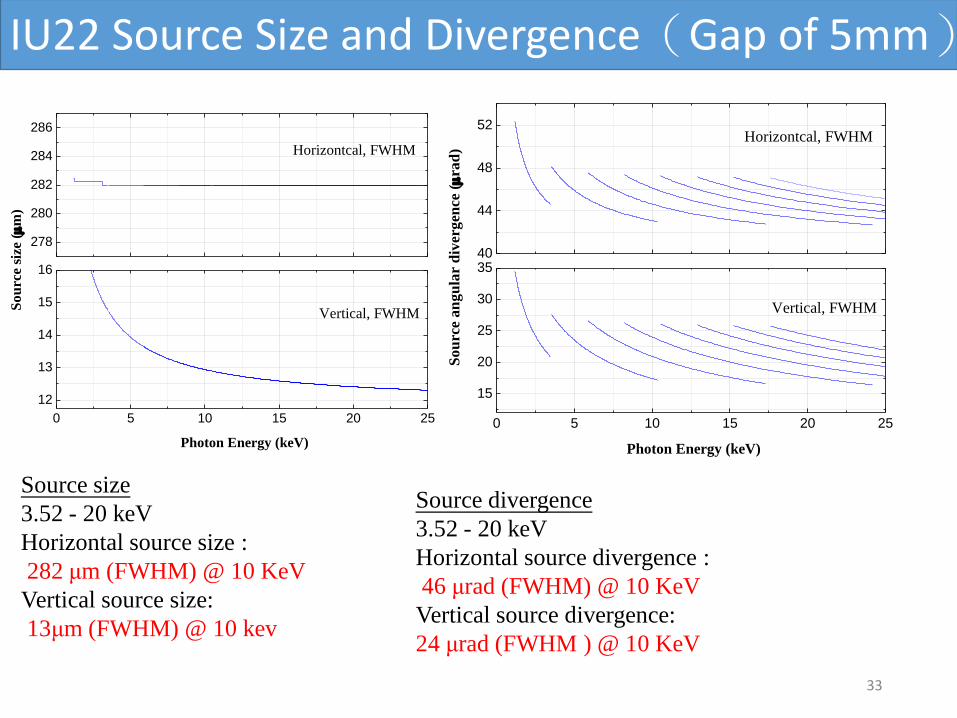
Source size
3.52 - 20 keV
Horizontal source size :
282 μm (FWHM) @ 10 KeV
Vertical source size:
13μm (FWHM) @ 10 kev
Source divergence
3.52 - 20 keV
Horizontal source divergence :
46 μrad (FWHM) @ 10 KeV
Vertical source divergence:
24 μrad (FWHM ) @ 10 KeV
278
280
282
284
286
0 5 10 15 20 25
12
13
14
15
16
So
urc
e si
ze (
m)
Photon Energy (keV)
Horizontcal, FWHM
Vertical, FWHM
40
44
48
52
0 5 10 15 20 25
15
20
25
30
35
So
urc
e an
gu
lar
div
erg
ence
(
rad
)Photon Energy (keV)
Horizontcal, FWHM
Vertical, FWHM
IU22 Source Size and Divergence(Gap of 5mm)

34
X-ray Methods With tens-nm resolution (incoherent)
•nano-XRF (x-ray fluorescence)
•Element-specific nanoimaging
•nano-XAFS (x-ray absorption fine structures)
•Local electronic structure
•Local chemical environments
•Element-specific, averaged over nanozied area
•nano-XEOL (x-ray excited optical luminescence)
•X-ray-to-visible down-conversion efficiency in nano phosphor
•nano-PXM (projection x-ray microscopy)
•Absorption and phase contrast x-ray images
•nano-CXDI (coherent x-ray diffraction imaging)
•Bragg-ptychograpgy •strain dynamics in nanodevices
Beyond sub-ten-nm resolution (coherent)

35
Estimation of the Data Rate
Type of experiment Maximum data rate (Bytes/second)
Explain
Fluorescence 8M Bytes/sec 1ms per pixel, 4096 channels with multi-element detector. 16 bits for each channel.
X-ray absorption 20 KBytes/sec 0.1ms per pixel 1 channel 16 bits for each pixel
•CDI/Bragg-ptychography 100M Bytes/sec
0.1 s per frame 2048x2048 16 bits for each pixel
Projection Microscope 100M Bytes/sec 20ms per frame @ 1024x1024 pixel number 16 bits for each pixel
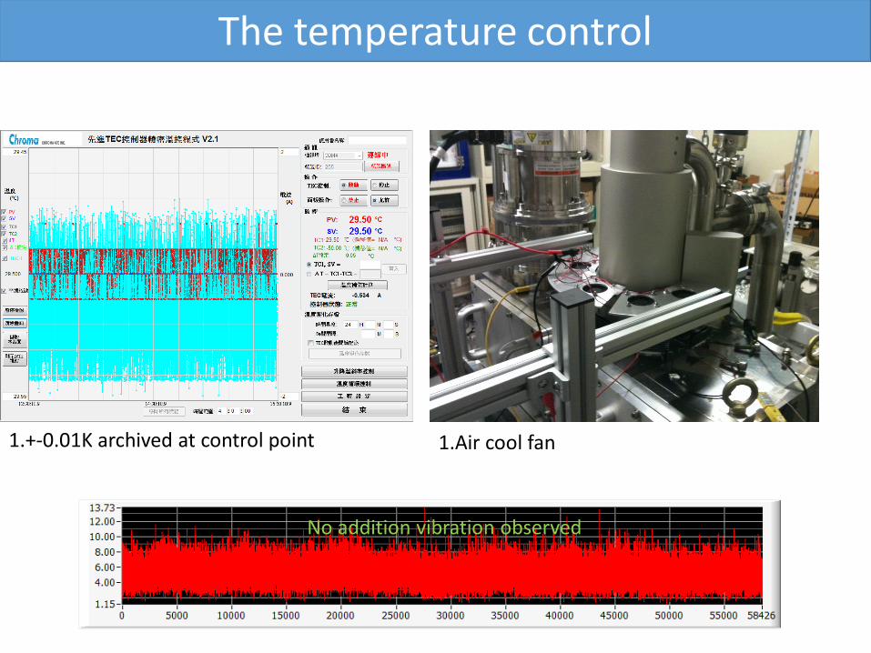
1.+-0.01K archived at control point 1.Air cool fan
No addition vibration observed
The temperature control

The consideration of XEOL

Scheme of the X-ray nanoprobe instruments
IU22
Focusing optics
Bragg-ptychography
Fluorescence
Detector
Projection CCD Sample
SEM
Laser interferometer
Sample Preparation Chamber
XEOL

39
Simulation of Beam Size
2 4 6 8 10 12 14 16 18 20
20
30
40
50
60
70
80
90
100
Foca
l sp
ot
(nm
)( F
WH
M)
Energy (keV)
diffraction-limit
geometrical
slope error = 0 rad
slope error = 0.05 rad
slope error = 0.10 rad
Diffraction limit
ε = 0.8895 λq/D
ε:resolvable image size
λ :wave length
q:image distance
D:projection of reflective surface on z-axis

40
Flux estimation of different focusing optics
4 5 6 7 8 9 10 11 12 13 14 1510
8
109
1010
1011
1012
1013
1014
1015
1016
1017
Source(ph/s/0.1w)
HFM 0.7 m, Zone plate
K-B Mirrors
HFM 0.7 m, Nested K-B mirrors
F
lux
(P
ho
ton
s/se
c)
Photon Energy (keV)
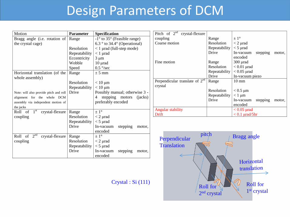
Pitch of 2nd
crystal-flexure
coupling
Coarse motion
Fine motion
Range
Resolution
Repeatability
Drive
Range
Resolution
Repeatability
Drive
± 1°
< 2 μrad
< 5 μrad
In-vacuum stepping motor,
encoded
300 μrad
< 0.01 μrad
< 0.05 μrad
In-vacuum piezo
Perpendicular translate of 2nd
crystal
Range
Resolution
Repeatability
Drive
10 mm
< 0.5 μm
< 1 μm
In-vacuum stepping motor,
encoded
Angular stability
Drift
< 0.05 μrad
< 0.1 μrad/5hr
Bragg angle
Roll for
1st crystal
pitch
Roll for
2nd crystal
Perpendicular
Translation
Motion Parameter Specification
Bragg angle (i.e. rotation of
the crystal cage)
Range
Resolution
Repeatability
Eccentricity
Wobble
Speed
-1° to 35° (Feasible range)
6.3 ° to 34.4° (Operational)
< 1 μrad (full-step mode)
< 1 μrad
3 μm
10 μrad
0.5 °/sec
Horizontal translation (of the
whole assembly)
Note: will also provide pitch and roll
alignment for the whole DCM
assembly via independent motion of
the jacks
Range
Resolution
Repeatability
Drive
± 5 mm
< 10 μm
< 10 μm
Possibly manual; otherwise 3 -
4 stepping motors (jacks)
preferably encoded
Roll of 1st crystal-flexure
coupling
Range
Resolution
Repeatability
Drive
± 1°
< 2 μrad
< 5 μrad
In-vacuum stepping motor,
encoded
Roll of 2nd
crystal-flexure
coupling
Range
Resolution
Repeatability
Drive
± 1°
< 2 μrad
< 5 μrad
In-vacuum stepping motor,
encoded
Design Parameters of DCM
Crystal : Si (111)