the elegance of line - global smt & packaging magazine · among the new types of solder-related...
TRANSCRIPT
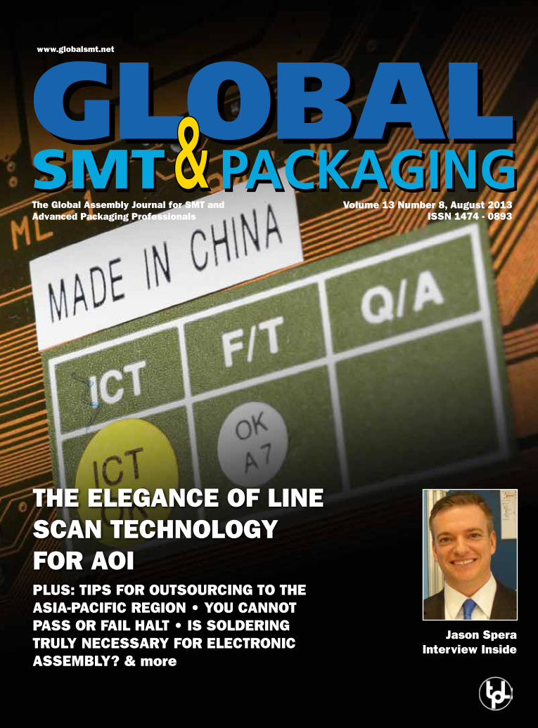
Jason SperaInterview Inside
The Global Assembly Journal for SMT and Advanced Packaging Professionals
Volume 13 Number 8, August 2013ISSN 1474 - 0893
www.globalsmt.net
PLUS: TIPS for oUTSoUrcING To The AsiA-PAcific region • You cAnnot PAss or fAil HAlt • is soldering trulY necessArY for electronic AssemblY? & more
The eLeGANce of LINe scAn tecHnologY for AoI
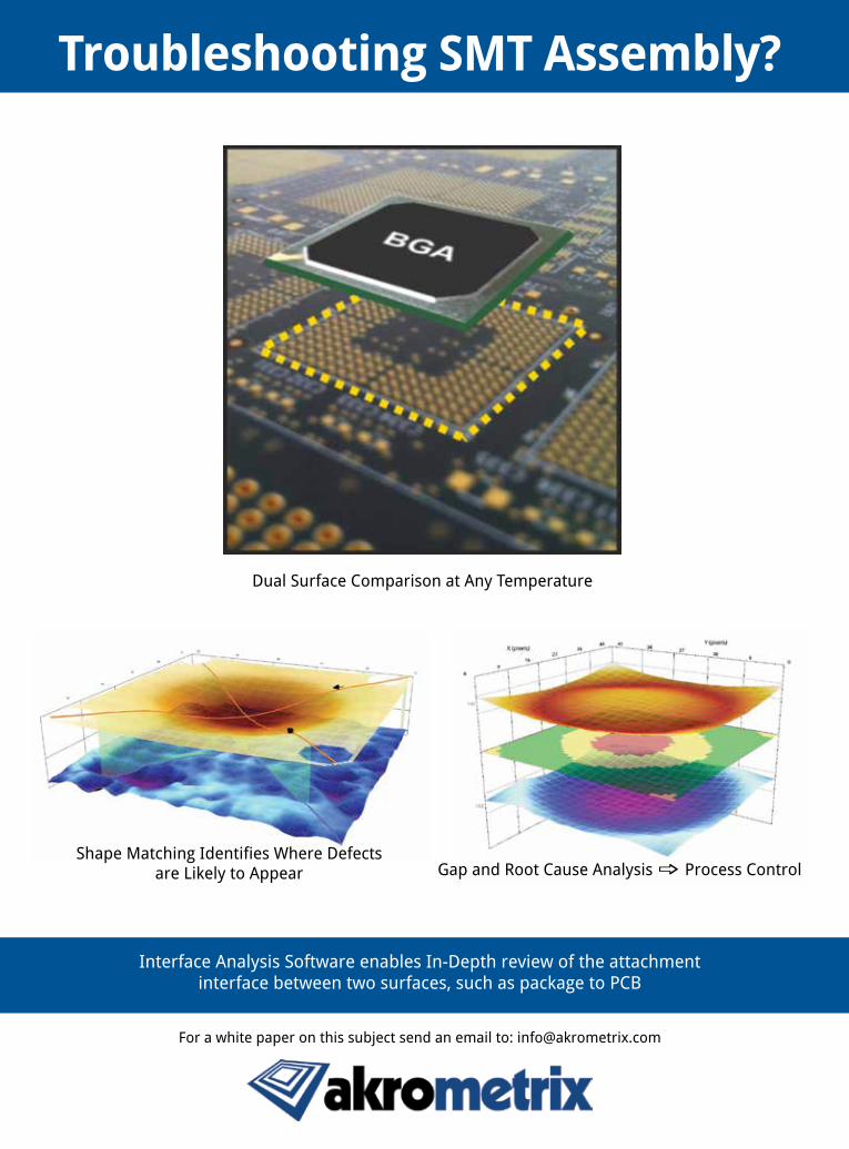
Troubleshooting SMT Assembly?
Interface Analysis Software enables In-Depth review of the attachment interface between two surfaces, such as package to PCB
For a white paper on this subject send an email to: [email protected]
Dual Surface Comparison at Any Temperature
Shape Matching Identifies Where Defectsare Likely to Appear Gap and Root Cause Analysis _ Process Control
akrometrix-GSP13.7.indd 1 6/18/13 9:16 AM
Global SMT & Packaging – August 2013 – 1www.globalsmt.net
Contents
Troubleshooting SMT Assembly?
Interface Analysis Software enables In-Depth review of the attachment interface between two surfaces, such as package to PCB
For a white paper on this subject send an email to: [email protected]
Dual Surface Comparison at Any Temperature
Shape Matching Identifies Where Defectsare Likely to Appear Gap and Root Cause Analysis _ Process Control
akrometrix-GSP13.7.indd 1 6/18/13 9:16 AM
Global SMT & Packagingis distributed by controlled circulation to qualified personnel. For all others, subscriptions are available at a cost of €135 for the current volume (twelve issues).
No part of this publication may be reproduced, stored in a retrieval system, transmitted in any form or by any means electronic, mechanical, photocopying, recording or otherwise without prior written consent of the publisher. No responsibility is accepted for the accuracy of information contained in the text, illustrations or advertisements. The opinions expressed in the articles are not necessarily those of the editors or publisher.
ISSN No. 1474-0893© Trafalgar Publications Ltd
Designed and Published byTrafalgar Publications Ltd,London, UKPrinted by Henrich Druck + Medien GmbH, Frankfurt, Germany
DownloAD ThiS iSSue To your Mobile Phone:
European edition
Visit www.globalsmt.net for the latest news and more, every day.
If you don’t already have one, search for a QR code reader app in your smartphone’s app marketplace. Then use it to scan the code above & download this magazine issue right to your phone.
Volume 13, No. 8
August 2013
contents
10
28
26
eDiToriAl2 China reforms will have global impact Trevor Galbraith
TeChnoloGy FoCuS10 The elegance of Line Scan Technology for AOI Mike Riddle, ASC International16 Tips for outsourcing to the Asia-Pacific region Jack Daniels, EastBridge Engineering
SPeCiAl FeATureS24 JPCA, Japan & the Industry: The Show Must Go On 26 Interview—Jason Spera, Aegis Software
reGulAr ColuMnS4 Is soldering truly necessary for electronic assembly? Joe Fjelstad18 Seasonal expansion with mixed patches of organic growth Walt Custer and Jon Custer-Topai25 Fan-in QFN packages fitting an expanding number of applications Sandra L. Winkler28 You cannot pass or fail HALT Craig Hillman30 Off shoring, on shoring—not suring? Keith Bryan
8 Industry News32 International Diary
oTher reGulAr FeATureS

Title
2 – Global SMT & Packaging – August 2013 www.globalsmt.net
editorial officesEuropeTrafalgar Publications Ltd.Globals SMT & PackagingCrown House, 72 Hammersmith Rd, Hammersmith, London, W14 8THUnited KingdomTel: +44 (0) 207 559 1467 Fax: +44 (0) 207 559 1468E-mail: [email protected]: www.globalsmt.net
United StatesTrafalgar Publications Ltd.Global SMT & PackagingPO Box 7579Naples, FL 34102, USATel: +1 (239) 245-9264Fax: (239) 236-4682
AsiaTrafalgar Publications Group Pvt LtdM-161/1 G.L. House, Gautam NagarBehind India Oil BhawanNew Delhi – 110049Office: +86 351 652 3813Fax: +86 351 652 0409
Editor-in-ChiefTrevor GalbraithTel: +44 7924 581 523 (Europe)Tel: +44 20 7792 0792 (UK)Tel: +1 (239) 245-9264 x101 (US)E-mail: [email protected]
Managing EditorTel: +1 (239) 245-9264 x108E-mail: [email protected]
China EditorLu ShuzhenE-mail: [email protected]
South East Asia Technical EditorDr Sripathy KarurEmail: [email protected]
Business Development/ Marketing ManagerElisangela DahlkeTel: +1 239 245 9264 x110E-mail: [email protected]
BillingTel: +1 (239) 245-9264 x106E-mail: [email protected]
Web DeveloperTorrence GermanyTel: +1 (239) 245-9264 x105E-mail: [email protected] AdvertisingEuropeAlex KlocksinCell: +49.1577.893.4884 (Ger.) [email protected] AmericaSandy DaneauTel: +1 (239) 245-9264 [email protected] Asia—IndiaAmitava [email protected]
Trevor GalbraithEditor-in-Chief
editorial
china reforms will have global impactLast week I made the annual sojourn to San Franscisco for SEMICON West and Intersolar. For those of you who didn’t know, Trafalgar Publications is active in both industries with Global SMT & Packaging and Global Solar & Alternative Energies magazines.
Two areas both magazines have in common is they are global in nature and rely heavily on Chinese-based manufac-turing, the solar/PV industry more so than electronics manufacturing. Somewhere in the region of 55% of global electronics assembly is performed in China, but that figure rises to around 85% for solar cell manufacturing and module assembly.
It has been well publicized that China’s growth has slowed to a more stately 7.5% per annum. But the IMF say even this growth rate is unsustainable without major reform. The world’s most populous nation is going through a transition from an export-led nation to one that manufac-tures principally for its indigenous people. To achieve that, a certain amount of finan-cial restructuring is required, and how the communist government handles that tran-sition will ultimately affect us all.
The old days of easy access to low interest soft loans from the government are coming to an end. According to some informed sources at Intersolar last week, the Chinese government is no longer guar-anteeing “Letters of Credit.” They have pushed that responsibility back onto the
local banks and told them that they have to assume the risk and the liability if these loans go bad. There are already a large number of companies, particularly in the PV industry, that are teetering on the edge, and their chances of securing loans from these banks are slim to none.
Therefore, we can expect a slew of bankruptcies in China, which some cynics believe is the Chinese way of pressing the reset button to try and return manufactur-ing industry to normalcy as quickly as pos-sible.
In other changes announced this week, the Chinese government is scrapping con-trols on the interest rates offered by the banks, heralding western-style competition to the Chinese lending market. Meanwhile, the G20 meeting in Moscow last week and formulated a plan to restrict the age-old practice of transfer-pricing and force large corporations to pay their fair share of tax.
What effect will this have on electronics manufacturing? It will accelerate the shift back to regional manufacturing practices, shortening the supply chain and limiting the risk.
—Trevor Galbraith.Editor-in-Chief
correction to the SMT Nuremberg review that appeared in issue 13.5:JUKI launched their new RX series of high volume placement systems. The next generation super high-speed flexible mounter, RX6, offers an IPC placement speed of 30,000 cph on a smaller footprint than the KE-3020 series. JUKI also demonstrated the new range of humidity controlled intelligent storage management (ISM) systems for automatic component inventory. The innovative and space-saving modules are available in three different configurations with a maximum capacity of up to 2,059 reels. Each system is entirely compatible with the Juki soft-ware IS and IFS-NX. Additionally, the IFS-NX traceability option can be linked in, guaran-teeing an all-round closed loop inventory management within the production environment.

New Jade FP
Performance Beyond Expectations

4 – Global SMT & Packaging – August 2013 www.globalsmt.net
is soldering truly necessary for electronic assembly?
There is an adage of long-standing that goes like this: “If the only tool in your tool chest is a hammer, the tendency
is to treat everything like a nail.” Such is the case of soldering in the electronics assem-bly industry. To be fair, solder was a reli-able workhorse in the electronics industry for many years… actually many decades. However, the forced implementation of lead-free solder that was foisted upon the electronics industry by the European Union altered forever that long-standing paradigm. The electronics industry now
struggles daily to meet the challenge of the lead-free solder mandate. The reader is invited to look at virtually any journal or newsletter on electronics manufacturing (including Global SMT & Packaging) and therein will be found article after article
and advertisement after advertisement on how to address problem after problem, nearly all of them related to the process of soldering.
The simple fact is that managing the electronics assembly process using solder technology, especially since the intro-duction of lead-free solder, has become increasingly complex. Moreover lead-free soldering has introduced to the industry a host of new types of defects and a number of new failure mechanisms (exclusive of the reintroduction of failure mechanisms which at one time had been fully put to rest, the most prominent being tin whiskers). Among the new types of solder-related defects are champagne voids, head-on-pillow defects, and poor wetting, to name but a few. While these defects are primarily related to the formation of a solder joint, a host of other types of defects have arisen that are artifacts of the higher-temperature soldering required for traditional SAC alloys. These include blistering of packages, excessive warpage of components, pad cra-tering, delamination of circuit boards, and others.
Post assembly processing, there is an ongoing challenge of cleaning baked-on fluxes in order to give the board a fight-ing chance at not evidencing ionic con-tamination failures at some point in the future. Clearly soldering, as faithful a servant as it has been over the years, has become as much a liability as it has been benefit. Given the challenge, a question that could or should rightfully be asked is “Is soldering really the only possible solution for making an electronics assembly?” The short answer is “No.”
The truth is that solderless intercon-nections have been used for many decades to make electrical and electronic intercon-nections. In the case of electrical intercon-nections, solderless interconnections go back to the 18th century, and perhaps even
earlier, when experimenters simply twisted wires together to make electrical intercon-nections. The method remains common today in the electrical wiring of electrical equipment as well as in nearly every home and building where wires are compressed into connector blocks using screws or by the use of wire nuts which are designed to force two or more wires into intimate physical contact, assuring a good electrical connection without using solder.
Elsewhere in electronics industry of today, solderless interconnection technol-ogy based on twisted wires persists in the form of “wire wrap” technology, where round wire is wrapped tightly to square posts or leads to make a reliable inter-connection. There is, as well, “press fit pin” technology, which has been used success-fully for decades to assemble connectors in the manufacture of backplane mother-boards. In practice, connectors with spe-cially designed pins are pressed into plated through holes of the backplane, making highly reliable interconnections between connector pins and plated through holes in the large backplanes used by the telecom-munications and internet server industry.
This particular solderless interconnec-tion method was developed because, like many of today’s printed board assemblies, the boards simply could not withstand the temperature and duration required of the soldering process to make a reliable inter-connection between the connector pins and the backplane. Even with traditional tin-lead solder, the temperature required for soldering was simply too high for the organic-resin-based laminate of the back plane to survive.
In the world of printed circuit manu-facture, there is a very specific terminology for one version the technology. It is called wire wrap, and it has been used as a method for making point-to-point interconnec-tions for prototypes and special small run
Joe Fjelstad
Is soldering truly necessary for electronic
assembly?
The simple fact is that managing the electronics assembly process using solder technology, especially since the introduction of lead-free solder, has become increasingly complex.
Alternative approaches to the manufacture of electronic assemblies bypass the soldering process and all of its shortcomings.
Dip Coating Systems | NANO-COAT
Ultra Precision Dip Coating Systems that can apply coatings from <60nm to >50μm at >3% accuracy.
Wizard Thermal Profi ling | ΔTDelta T - Wizard Thermal Pro� ling - a 5 channel temperature logger and user friendly software.
Capable - Simple - Adaptable - Flexible - Accurate - Economic
Solder Paste Inspection | Z-Check
Non-contact solder paste measuring systems, designed to provide accurate pad speci� c measurement of solder paste deposits, adhesives and component placement.
Solder Dross Recovery | Solder Saver™
The Solder-Saver o� ers companies who use ‘wave soldering’ the opportunity to instantly recycle dross created in the wave solder pot, thereby saving up to 50% in new solder bar purchases.
B2, Armstrong Mall, Southwood Business Park, Farnborough, Hampshire, GU14 0NR. UK
Call +44 (0)12 5252 1500 orvisit www.gen3systems.com
NEW from Gen3 Systems
Contamination Testing | CMBBT
Optimised to provide the most accurate measurements, the system features a “Narrow & Deep” tank to avoid the unwanted in� uences of CO2.

6 – Global SMT & Packaging – August 2013 www.globalsmt.net
is soldering truly necessary for electronic assembly?
products for more than four decades. In the process, a wire is wrapped multiple times around a metal post to make electrical interconnection. Since the pin is normally a square post, the soft copper wire deforms around the pin, creating a gas-tight con-nection, assuring a long, reliable life.
While not a direct descendant of wire wrap technology, there is another way of making solderless interconnection between boards, based on the use of specially fab-ricated wires called twisted wire intercon-nect. The approach has been around for a number of years, having been developed initially by Cray Computer Corporation in the late 80’s. The technology is now avail-able from Medallion Technology (www.medalliontech.com), as the industry begins to face some of the challenges that faced Cray Computer at that time. The funda-mental unit of TWI technology is based on a twisted wire bundle of a high modu-lus (i.e. spring-like) metal that, by means of a specially developed tool, is clamped on one end and then twisted in reverse to unwind the wires, creating something that looks similar to a string of small birdcages. These “spring bulges” can then be inserted into plated through hole vias to make interconnection between traditional PCB assemblies where required. (Please visit the company’s website for more information.)
There are other types of solder-free metallurgical interconnection technologies that are worth mentioning: sintered pastes (which have seen renewed interest in recent months with an announcement and articles by both Ormet and Sumitomo) and transient liquid phase joining and welding. The sintered paste solution is somewhat similar to soldering except that the mate-rials used are different, and the joining temperatures are lower. Transient liquid
phase bonding is somewhat of a hybrid of soldering and welding, in that two metals are joined by heat and pressure. The metals react instantly once joining temperature is achieved, and the resulting alloy has a melt-ing temperature above either of the two joining metals.
The last of the just-mentioned list of solderless interconnection alternatives is welding. Welding can be accomplished by several different methods, including the use of lasers and resistance welding. The former case is fairly well known; the latter is less common. In the process, the leads of a device are welded to the circuit by com-pleting a momentary high current circuit with pressure applied, resulting in a metal-lurgical weld being formed between lead and circuit. This process is relatively slow but may be of use in certain applications.
In addition to the mechanical intercon-nection solutions just reviewed, there are a host of adhesive-based technologies that have been, and still are being, successfully used to make electromechanical intercon-nections. In general, there are three basic types of adhesive based interconnections: conductive, anisotropic and non-conduc-tive.
The first type of adhesive used for making interconnection without solder is comprised of a resin mixed with a con-ductive material, most commonly silver, though there is an increasing interest in carbon-based nanomaterials. Conductive adhesives have been used in applications where the component is heat sensitive. An example of one such application is with plastic encapsulated LEDs. Such adhesives are also commonly used with membrane switch assemblies, which are typically fab-ricated using screen-printed or stenciled silver ink conductors.
The second type is anisotropic conduc-tive adhesive, in film or liquid form. Such adhesives are infused with widely dispersed conductive particles that, in use, allow for the conduction of electricity in the Z axis but not in X nor Y directions. These join-ing materials are very commonly used for the interconnection of display driver cir-cuits used to deliver the signals to various types of flat panel displays. The advantage of this type of adhesive is that it can reliably make the very fine pitch interconnections required for such applications.
The last type is nonconductive adhesive that can be used where signals are capaci-tively coupled or where operating voltages are sufficiently high to break through the thin bond line. Also, in some cases a metal feature will actually pierce the adhesive.
Still it is the first two adhesive methods that see the greatest use.
Finally, there is the method that has been the subject of discussion a number of times over the last several years in this space and elsewhere, and that is the Occam approach, wherein electrical interconnec-tions between circuits and components are made almost exclusively by electroplating copper. This approach is being increasingly looked to for the manufacture of assemblies that are the reverse of traditional products, in that rather than putting components on circuit boards, circuits are built up on component boards. A fairly recent article describing an aluminum circuit board using the solder-free methods alluded to can be found in GSMT&P archives of this column.
In summary, solder, while it has certain advantages, also has a growing list of liabili-ties. History and recent advances in tech-nology provide credence to the belief that it is not necessary for electronic assembly in many if not most instances. That said, solder is an incumbent technology with a long history of its own, and despite the abu-sive challenges thrust upon the industry by the lead-free mandate, solder continues to be used, and this will go on for many years to come.
However, what is appealing to some of the more enlightened technologists in the industry is the knowledge that reliable solder-free solutions are out there, both on the horizon and in the past. Maybe having a tool other than just a hammer might be an appealing thought to other technolo-gists in the industry at some point as well.
Verdant Electronics founder and president Joseph (Joe) Fjelstad has more than 40 years of international experience in electronic interconnection and packaging technology in a variety of capacities from chemist to process engineer and from international consultant to CEO. Mr. Fjelstad is also a well known author writing on the subject of electronic interconnection technologies. Prior to founding Verdant, Mr. Fjelstad co-founded SiliconPipe a leader in the development of high speed interconnection technologies. He was also formerly with Tessera Technologies, a global leader in chip-scale packaging, where he was appointed to the first corporate fellowship for his innovations. He has 150 US patents to his credit.
A host of adhesive-based technologies have also been, and still are being, successfully used to make electromechanical interconnections.
w w w . m i r t e c . c o m
JOIN...the Winner’s Circle!
AW A R D S
AN
D
C O U N T I NG
MS-153D SPI
MV-92D/3D AOI
MW-MI-23-Mirtec-ad_203x275_Global.indd 1 4/11/13 10:30 AM

w w w . m i r t e c . c o m
JOIN...the Winner’s Circle!
AW A R D S
AN
D
C O U N T I NG
MS-153D SPI
MV-92D/3D AOI
MW-MI-23-Mirtec-ad_203x275_Global.indd 1 4/11/13 10:30 AM
Title
8 – Global SMT & Packaging – August 2013 www.globalsmt.net
Viscom’s Michael Mügge is named the new deputy head of the fed regional group hanover
Michael Mügge, sales engineer at Viscom, is the new deputy head of the Professional Association of Electronics Designs‘ (FED) regional group Hanover. The head of the regional group is Ruud Wilms from the GED Society for Electronics and Design mbH. Michael Mügge succeeds Volker Spitzer from WABCO, who for personnel reasons, has given up this honorary post, but remains a personnel member of the
FED. The selection took place on June 5th during the FED’s regional group meeting at the GED GmbH in Hanover.www.viscom.de
Venne electronics doubles smt capacity with mYdAtAIn response to dramatic growth in its order input, Venne Electronics has recently installed a new high-throughput MYDATA SMT production line. The new Synergy line comprises of two of MYDATA’s latest MY100DXe14 machines working in tandem, and replaces the company’s exist-ing SMT line, which used older MYDATA equipment. The new line almost doubles Venne’s SMT production capacity, but cru-cially it requires no more floor space than the line it replaces, and it’s operated by the same number of staff.www.venne.nl
Pillarhouse appoints eTeK Ireland as S. Ireland repSelective soldering machine manufacturer Pillarhouse International Ltd appointed the newly formed ETEK Ireland Ltd to represent
its range of machines in Southern Ireland.Based in the UK Pillarhouse International Ltd is a leading specialist manufacturer of Selective Soldering Systems and prides itself on consistently leading new technol-ogy development. www.pillarhouse.co.uk
LPKf laser welding expands
Since being set up in 2001, LPKF’s laser plastic welding department has seen its workforce grow to more than 100 employ-ees. Despite repeated expansions at the cur-rent location in Erlangen it is bursting out of its seams. As already announced by man-agement, LPKF has now acquired a produc-tion building that offers growth potential for this area of the business.www.lpkf.de
european semiconductor industry leading indicator and forecast outlook improveEconomic research firm e-forecasting.com today announced that the European Semiconductor Sales leading indicator edged up 0.1% in May to a reading of 139.6 after gaining 0.5% in April. The index was set to average 100 in 2005. The indicator, comparable to the company’s other global regional semiconductor industry indicators for North America, Asia Pacific and Japan, is a forward-looking composite index that forecasts six months ahead, on average, business activity in the region for sales for semiconductors. e-forecasting.com
Microtechnology experts expect no strain on trade relations with chinaLeading representatives of the European microtechnology industry do not expect that the current conflict will put a strain on the trade relations between Europe and China. In a flash poll, 57 percent of partici-pating experts from industry and science saw no cause for concern. Only 13 percent
Industry news
Gen3 Systems awarded contract for the KISS 103 selective soldering system to ZoT engineering, ScotlandManufactured by ACE Production Technologies, the KISS systems,“(Keep it Simple Soldering”) were first introduced in 2005. KISS-103 System for Zot Engineering is designed to process 460mm x 600mm assemblies entirely without intervention and is the biggest system in the KISS range. Automatically applying flux and solder to through-hole component leads without disturbing neighbouring SMT components, they provide solder quality that is significantly superior to hand soldering with full barrel fill and top side fillets consistently produced. www.gen3systems.com
industry news
Global SMT & Packaging – August 2013 – 9www.globalsmt.net
supposed that the conflict about punitive duties will have a lasting impact on the trade relations.
havant-based outsource electronics Limited now part of Season GroupSeason Group has completed the acqui-sition of Outsource Electronics Limited (OEL) in the UK. The deal follows the acquisition of leading UK embedded computer systems company, DSP Design in Chesterfield, East Midlands, in 2012 and forms part of the group’s strategy to grow its global offering in line with cus-tomer demand. www.seasongroup.com, www.outsourceelectronics.co.uk
Premier farnell expands global partnership with emerson Network PowerPremier Farnell plc has announced the expansion of its partnership with Emerson Network Power. Already a distributor of Emerson Connectivity Solutions product lines, this agreement will bring the popular lines of Johnson and Trompeter RF connec-tivity products to customers in both Asia Pacific and Europe. Currently European customers have access to the Semflex DKT cable assemblies. Emerson Connectivity Solutions and Premier Farnell have part-nered to provide design engineers with quality products and outstanding service via Premier Farnell’s trading brands ele-ment14 (Asia Pacific), Farnell element14 (Europe) and Newark element14 (North America). www.premierfarnell.com
IPTe factory Automation appoints representative in Tunesia and AlgeriaIPTE Factory Automation is now work-ing with Adelec International as its new representative for Tunesia and Algeria. Started July 1st, Adelec International will supply sales as well as customer services for IPTE in Tunesia and Algeria. Adelec International will be represented by Aziz Lahimer, General Manager. According to IPTE Factory Automation, this collabora-tion will strengthen the company’s access to the Tunesia and Algeria market, while at the same time, ensuring better support to the customers. www.ipte.com
PVA announces new sales manager for europeGlobal manufacturer and supplier of conformal coating and precision dis-
pensing systems, PVA (Precision Valve & Automation, Inc.) is please to announce that Regional Sales Manager Erin Vickers’ territory has been expanded to include responsibilities for Europe. With a suc-cessful tenure in her current territory, including acquiring several new custom-ers, closing over 40% more projects than any other sales manager, bolstering the Sales Representatives, and developing and meeting sales goals & plans, Vickers is well prepared to oversee operations for Europe. www.pva.net
GoePeL electronic expands gAte program in denmarkGOEPEL electronic announces the extended incorporation of CIM Industrial Systems A/S into the global alliance program GATE™ (GOEPEL Associated Technical Experts). CIM will focus in par-ticular on application development and practical implementation of new JTAG/Boundary Scan based solutions as well as their integration into existing test systems. www.goepel.com
counterfeit detection testing service to combat fraudulent componentsThe electronics industry is currently wit-nessing a growth in component counter-
feiting in which the supplier of parts to the assembler is often unaware. The complex-ity of the supply chain and the ingenuity of the counterfeiter mean it can be extremely difficult to detect that electronic compo-nents are counterfeit. Consequently, ITRI Innovation is offering a counterfeit detec-tion testing service aiming to verify elec-tronic components. www.itri.co.uk
JoT Automation receives global award for customer value leadershipJOT Automation has been recognized for its continued work to deliver innovative solutions and developments to meet its business markets with the Frost & Sullivan Award for Customer Value Leadership. Frost & Sullivan saw JOT as a company that takes substantial effort to design and deliver innovative solutions that are in sync with emerging technological advancements. JOT’s frequent product introductions and enhancements, and its strategic decision to extend its business markets, have enabled it to develop close relationships with its customers.www.jotautomation.com
industry news
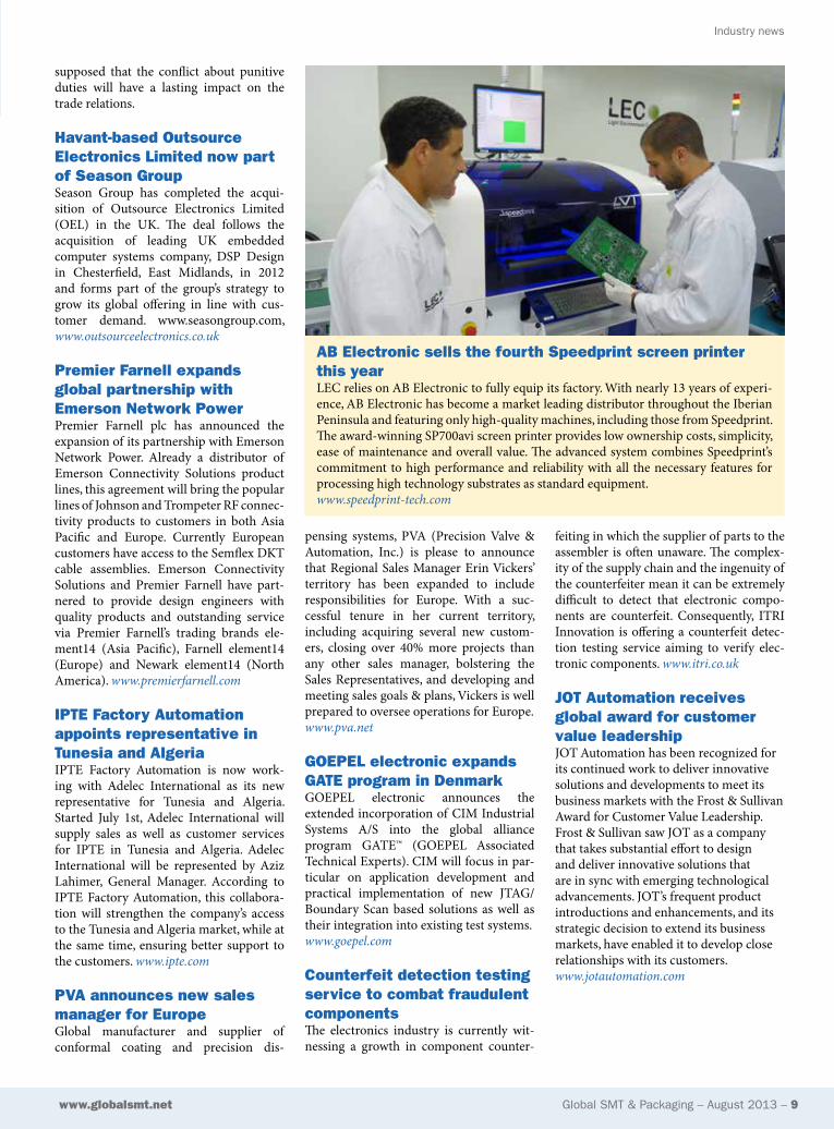
AB electronic sells the fourth Speedprint screen printer this yearLEC relies on AB Electronic to fully equip its factory. With nearly 13 years of experi-ence, AB Electronic has become a market leading distributor throughout the Iberian Peninsula and featuring only high-quality machines, including those from Speedprint. The award-winning SP700avi screen printer provides low ownership costs, simplicity, ease of maintenance and overall value. The advanced system combines Speedprint’s commitment to high performance and reliability with all the necessary features for processing high technology substrates as standard equipment. www.speedprint-tech.com

10 – Global SMT & Packaging – August 2013 www.globalsmt.net
The elegance of line Scan Technology for Aoi
And the answer seems simple enough: employ additional cameras, surrounding the downward-looking principle camera, and position them at oblique angles so that they can provide a “side view” of the region of interest, capturing images of defects that seem undetectable from overhead.
But drilling deeper into this solution uncovers several questions:1. There are some AOI systems on the
market that tout using up to eight cameras. So, how many cameras are enough?
2. How does an AOI system process the images generated by these multiple cameras to produce useable inspection data? Typically, most AOI systems with side view cameras perform only image comparison on side view data. In other words, they use a “golden” image gener-ated from one or multiple samples as a model and compare that golden image to the current area of interest. But what happens if the area of interest is good, but there is a difference in color or lighting, or board-to-board, lot-to-lot variations? Will the same golden image work on the same component package type placed anywhere on the PCB…in
any orientation? In other words, can one use the same component library no matter where the component is located, or what taller components sur-round it (shadowing issues)? Does a multiple camera system take more time to program and debug? Does increas-ing the number of cameras increase the number of false failures or false calls?
3. How sensitive is the calibration and alignment of the optical system on an AOI using multiple cameras?
4. How reliable is an AOI system using additional cameras? Does attaching more sensitive hardware make it more prone to mechanical and electrical problems in a production environ-ment?
5. How does adding more cameras (and more images to process) affect the inspection speed?
6. What does the additional hardware—as well as the software to support it—add to the price and operating cost of the AOI system?
Line Scan Technology may offer an elegant alternative to multiple camera AOI systems. Since the mid-1990s, SAKI
There seems to be a trend in the AOI market: more is better. On the surface this trend seems logical, because how can just one single downward-looking FOV (field-of-view) camera circled by a ring light detect production errors in solder quality, lifted leads…head-in-pillow defects?
Mike Riddle, ASC International
The elegance of Line Scan Technology for AoI
Figure 1. Line Scan Technology
Since the mid-1980s, Mike Riddle has worked in electronics inspection and test, helping companies with leading edge technologies find their paths to market leadership. Customer-focused and growth-oriented, Mike has held various roles in business development, marketing, sales and international distribution. He is currently serving as AOI Product Manager for ASC International. You can learn more about Mike by visiting: http://www.linkedin.com/pub/mike-riddle/12/491/710
Global SMT & Packaging – August 2013 – 11www.globalsmt.net
The elegance of line Scan Technology for Aoi
Corporation has employed this reliable yet flexible machine vision concept in over 7,000 AOI installations worldwide, mostly in high-production environments across Asia. This paper will provide an explana-tion of Line Scan Technology and how it’s being applied in AOI to solve difficult inspection problems such as soldering and lifted lead defects without the use of addi-tional imaging hardware.
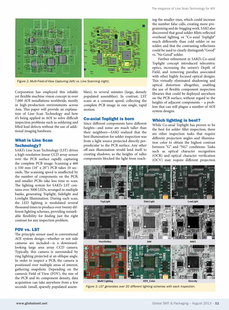
What is Line Scan technology? SAKI’s Line Scan Technology (LST) drives a high-resolution linear CCD array sensor over the PCB surface rapidly capturing the complete PCB image. Scanning a 460 x 550 mm (18” x 20”) PCB takes 10 sec-onds. The scanning speed is unaffected by the number of components on the PCB, and smaller PCBs take less time to scan. The lighting system for SAKI’s LST con-tains over 3000 LEDs, arranged in multiple banks, generating Toplight, Sidelight and Lowlight Illumination. During each scan, the LED lighting is modulated several thousand times to produce over twenty dif-ferent lighting schemes, providing remark-able flexibility for finding just the right contrast for any inspection problem.
foV vs. LST The principle sensor used in conventional AOI system design—whether or not side cameras are included—is a downward-looking large area array CCD camera. Typically, this camera is surrounded by ring lighting projected at an oblique angle. In order to inspect a PCB, the camera is positioned over multiple areas of interest, gathering snapshots. Depending on the camera’s Field of View (FOV), the size of the PCB and its component density, data acquisition can take anywhere from a few seconds (small, sparsely populated assem-
blies), to several minutes (large, densely populated assemblies). In contrast, LST scans at a constant speed, collecting the complete PCB image in one single, rapid motion.
co-axial Toplight is born Since different components have different heights—and some are much taller than their neighbors—SAKI realized that the best illumination for solder inspection was from a light source projected directly per-pendicular to the PCB surface. Any other off-axis illumination would lend itself to creating shadows, as the heights of taller components blocked the light from reach-
ing the smaller ones, which could increase the number false calls, creating more pro-gramming and de-bugging work. SAKI also discovered that good solder fillets reflected overhead lighting or “Co-axial Toplight” much differently than cold solder or no solder, and that the contrasting reflections could be used to clearly distinguish “Good” vs. “No Good” solder.
Further refinement in SAKI’s Co-axial Toplight concept introduced telecentric optics, increasing the sensor’s Depth of Field, and removing parallax associated with other highly focused optical designs. This virtually eliminated shadowing and optical distortion altogether, enabling the use of flexible component inspection libraries that could be deployed anywhere on the PCB surface, without regard to the heights of adjacent components – a prob-lem that can still plague a number of AOI system designs.
Which lighting is best?While Co-axial Toplight has proven to be the best for solder fillet inspection, there are other inspection tasks that require different projection angles and illumina-tion color to obtain the highest contrast between “G” and “NG” conditions. Tasks such as optical character recognition (OCR) and optical character verification (OCV) may require different projection
Figure 2. Multi-Field-of-View Capturing (left) vs. Line Scanning (right).
Figure 3. LST generates over 20 different lighting schemes with each inspection.
12 – Global SMT & Packaging – August 2013 www.globalsmt.net
The elegance of line Scan Technology for Aoi
angles—as well as data from multiple pro-jection angles—to accurately determine that the correct part has been placed. In some cases, the color of the component is used to detect presence/absence, or the correct part. Color inspection usually requires another unique illumination set-ting. In some cases, the contrast of color and/or reflectivity between the component and the substrate is very subtle. This may require a special, “user-defined” lighting scenario to highlight the differences that will provide repeatable results.
To enhance its Co-axial Toplight concept, SAKI added banks of LEDs to project off-axis “Sidelight”, which has been found best for color inspection and “Lowlight”, which uses a very acute projec-
tion angle, and is ideal for OCR and OCV inspection tasks. Further testing dem-onstrated that sometimes a combination such as “Toplight-Sidelight” or “Sidelight-Lowlight” produced superior results. Still, SAKI discovered other inspection tasks requiring even more lighting options. Rather than add more lighting hardware and creating more servicing issues, SAKI decided to solve the problem using soft-ware. Today, with each scan of the PCB, SAKI AOI systems generate over twenty different lighting schemes. Any one of those lighting schemes—plus a user-defined option that allows the user to decide the best Toplight/Sidelight/Lowlight blend—can be applied to any inspection window and algorithm used in any component
library. This lighting flexibility—unique to the industry—employs a very simple elec-tro-mechanical design to accomplish what other systems strive for using complex hardware. Furthermore, producing these numerous lighting schemes generates no impact on scanning time.
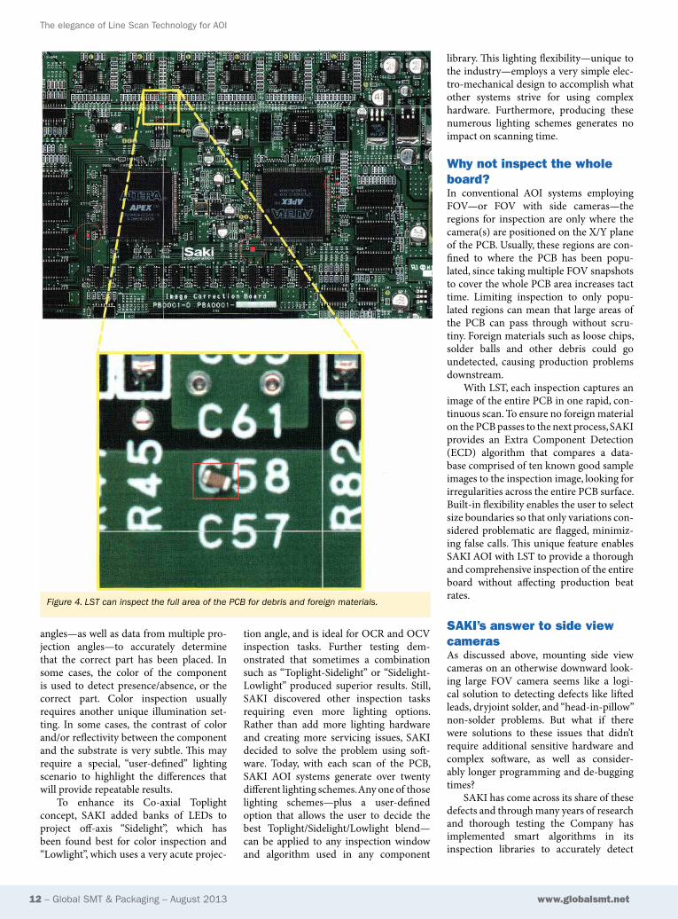
Why not inspect the whole board?In conventional AOI systems employing FOV—or FOV with side cameras—the regions for inspection are only where the camera(s) are positioned on the X/Y plane of the PCB. Usually, these regions are con-fined to where the PCB has been popu-lated, since taking multiple FOV snapshots to cover the whole PCB area increases tact time. Limiting inspection to only popu-lated regions can mean that large areas of the PCB can pass through without scru-tiny. Foreign materials such as loose chips, solder balls and other debris could go undetected, causing production problems downstream.
With LST, each inspection captures an image of the entire PCB in one rapid, con-tinuous scan. To ensure no foreign material on the PCB passes to the next process, SAKI provides an Extra Component Detection (ECD) algorithm that compares a data-base comprised of ten known good sample images to the inspection image, looking for irregularities across the entire PCB surface. Built-in flexibility enables the user to select size boundaries so that only variations con-sidered problematic are flagged, minimiz-ing false calls. This unique feature enables SAKI AOI with LST to provide a thorough and comprehensive inspection of the entire board without affecting production beat rates.
SAKI’s answer to side view camerasAs discussed above, mounting side view cameras on an otherwise downward look-ing large FOV camera seems like a logi-cal solution to detecting defects like lifted leads, dryjoint solder, and “head-in-pillow” non-solder problems. But what if there were solutions to these issues that didn’t require additional sensitive hardware and complex software, as well as consider-ably longer programming and de-bugging times?
SAKI has come across its share of these defects and through many years of research and thorough testing the Company has implemented smart algorithms in its inspection libraries to accurately detect
Figure 4. LST can inspect the full area of the PCB for debris and foreign materials.
C
M
Y
CM
MY
CY
CMY
K
C
M
Y
CM
MY
CY
CMY
K
14 – Global SMT & Packaging – August 2013 www.globalsmt.net
The elegance of line Scan Technology for Aoi
and report these production errors using the power of its LST and flexible lighting technology. Below are a few examples of how these algorithms work:
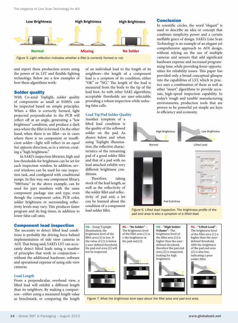
Solder qualityWith Co-axial Toplight, solder quality of components as small as 01005s can be inspected based on simple principles. When a fillet is correctly formed, light projected perpendicular to the PCB will reflect off at an angle, generating a “low brightness” condition, and produce a dark area where the fillet is formed. On the other hand, when there is no fillet—as in cases where there is no component or insuffi-cient solder—light will reflect in an equal but opposite direction, as in a mirror, creat-ing a “high brightness.”
In SAKI’s inspection libraries, high and low thresholds for brightness can be set for each inspection window. In addition, sev-eral windows can be used for one inspec-tion task, and configured with conditional jumps. In this way, one component library, “0805smc” in the above example, can be used for part numbers with the same component package size and type, even though the component color, PCB color, solder brightness or surrounding reflec-tivity levels may vary. This produces faster program and de-bug times, in addition to lower false call rates.
component lead inspectionThe necessity to detect lifted lead condi-tions is probably the driving force behind implementation of side view cameras in AOI. That being said, SAKI’s LST can accu-rately detect lifted leads using a number of principles that work in conjunction—without the additional hardware, software and operational expense of using side view cameras.
Lead LengthFrom a perpendicular, overhead view, a lifted lead will exhibit a different length than its neighbors. By making a compari-son—either using a measured length value as benchmark, or comparing the length
of an individual lead to the length of its neighbors—the length of a component lead is a symptom of its condition, either “OK” or “NG.” The length of the lead is measured from the body to the tip of the lead foot. As with other SAKI algorithms, acceptable thresholds are user-selectable, providing a robust inspection while reduc-ing false calls.
Lead Tip/Pad Solder QualityAnother symptom of a lifted lead condition is the quality of the reflowed solder on the pad. As shown below and when using Toplight illumina-tion, the reflective charac-teristics of the remaining pad of a good solder fillet and that of a pad with no lead attached exhibit very different brightness con-ditions.
Therefore, taking stock of the lead length, as well as the reflectivity of the solder fillet and reflec-tivity of pad end, a lot can be learned about the condition of a component lead solder fillet.
conclusionIn scientific circles, the word “elegant” is used to describe an idea or concept that combines simplicity, power and a certain ineffable grace of design. SAKI’s Line Scan Technology is an example of an elegant yet comprehensive approach to AOI design, without relying on the use of multiple cameras and sensors that add significant hardware expense and increased program-ming time, while providing fewer opportu-nities for reliability issues. This paper has provided only a broad conceptual glimpse into the capabilities of LST, which in prac-tice uses a combination of these as well as other “smart” algorithms to provide accu-rate, high-speed inspection capability. In today’s ‘rough and tumble’ manufacturing environments, production tools that are proven to be powerful yet simple are keys to efficiency and economy.
Figure 5. Light reflection indicates whether a fillet is correctly formed or not.
Figure 6. Lifted lead inspection. The brightness profile of the pad end area is also a symptom of a lifted lead.
OK – Using Toplight illumination, the brightness level of the fillet area (1) is low. If the value of (1) is below a user defined threshold, the pad end area (2) will not be inspected.
NG – “No Solder” – The brightness level of the fillet area (1) is ≥ the brightness in the pad end (2).
OK – “High Solder Volume”– The brightness level of the fillet area (1) is higher than the user-‐defined threshold, therefore the pad end area (2) is inspected, looking for high brightness.
NG – “Lifted Lead”– The brightness level of the fillet area (1) is higher than the user-‐defined threshold, AND the brightness of the pad end area (2) is also low, indicating a poor solder fillet.
Figure 7. What the brightness level says about the fillet area and pad end area.

© 2013 Panasonic Corporation of North America. All rights reserved.
Combines the capability, flexibility, and reliability you expect from Panasonic into a cost-effective, high-mix solution
Incrementally scalable, single platform solution for versatile production in High Mix or New Product Introduction environments
Regardless of your mix or volume, Panasonic’s new AM100 can help improve throughput and efficiency,
while keeping your quality reliably high
panasonicfa.com/am
A new, cost-effective, high-mix PCBA solution
AM100
pfsa_gsmt_aug13.indd 1 7/22/13 3:43 PM
16 – Global SMT & Packaging – August 2013 www.globalsmt.net
Tips for outsourcing to the Asia-Pacific region
Now that the commercial and industrial infrastructure of the Asia-Pacific region has reached a stable and sustainable level, many companies are considering establish-ing purchasing programs there. You can’ t really blame them. Drawn by the opportu-nity to lower costs, broaden supplier bases and localize supply for Asia-Pacific region manufacturing sites, there is a flood of RFQs rushing into the region.
Asia is now a great place to do busi-ness, but like any venture, you should do your due diligence before committing your company to any overseas ventures. Here are some guidelines to follow before doing business in the Asia-Pacific region:
Pick your products carefullyWhile almost any class of product can be purchased in Asia, not all make economic or strategic sense. Products that have a majority of their value tied to their raw material content rather than the “value add” probably should be purchased close to home. A good example of this model
is the printed circuit board and intercon-nect segment. Copper clad laminate and prepreg (pre-impregnated polymer/glass adhesive layers) represent a minority of the value in most PCBs. These raw mate-rials can be procured in most countries and the processes used to generate them are highly automated. Even with Asian labor rates at less than 30 percent of the US norm, these materials may cost less in the States. A better play in this market is to purchase fully assembled printed circuit boards (PCBA), which have a higher “value density”.
Know your supplierThe physical and cultural distance between you and your supplier is magnified when trading in Asia. As a general rule, engage with a new supplier through their agents and representatives at the beginning of the relationship. To minimize the gulf and establish a productive relationship, you need to pick up, go and hold face-to-face meetings with members of the prospective
Now that the commercial and industrial infrastructure of the Asia-Pacific region has reached a stable and sustainable level, many companies are considering establishing purchasing programs there. You can’ t really blame them. Drawn by the opportunity to lower costs, broaden supplier bases and localize supply for Asia-Pacific region manufacturing sites, there is a flood of RFQs rushing into the region.
Jack Daniels, EastBridge Engineering
Tips for outsourcing to the Asia-Pacific region
Global SMT & Packaging – August 2013 – 17www.globalsmt.net
Tips for outsourcing to the Asia-Pacific region
suppliers’ management teams. It is essen-tial to interview key executives, tour their facilities and ask for and check references.
The corporate structure and ownership of companies in Asia can often be murky and, at times, beyond comprehension. A useful start to your due diligence exercise can occur when arriving at the factory. Does the name on the sign match the name on the quotation? There may be a logical reason why it doesn’t, but is pays to find out.
Build a relationship of communicationWhile most Asian suppliers employ at least one proficient English speaker, their mother tongue isn’t English (and often a second or third more exotic dialect). There are significant culture-based differ-ences in communications styles around the world. In China, the boldly stated response of “yes” or “no problem” often means “I acknowledge your question” or “we’ll try it once”.
A productive approach when meeting to review specifications, discuss scale-up plans and negotiate pricing is to proceed slowly. Speak slowly, avoid slang, jargon
and contractions and pause often to review key points. It is also useful to collaborate on a meeting summary, written on the white board, before leaving the conference room.
If you decide to move ahead with a new supplier, we recommend assigning a “Communications Specialist” within your organization. Learning to navigate one another’s organization chart, phone tree and mix of personalities is a daunting task, in both directions. Your Communications Specialist should be the “go-to” person, who can field all questions related to the procurement project.
It’s all in the termsSpecial attention should be paid to com-mercial and shipping terms, usually referred to as “INCOTERMS”. If you’re accustomed to doing business domestically, most often the goods are shipped EXW (Ex-Works) or FOB (Free On Board). In Asia, the range of shipping methods is much broader, as is the responsibility matrix associated with the associated terms. It’s your responsi-bility to understand when the title to the goods changes hands and which party is responsible for each element of the freight charges.
Discuss which INCOTERM is most appropriate for your company and model the costs and risks before sealing the deal.
Be patientMost Asian suppliers are building their businesses for the long haul. They’ve made significant investments in machinery, waste treatment equipment, ERP and training. They’re not fly-by-night counterfeiters. If you put in the time and build a relation-ship, or guanxi in Mandarin you will have a dedicated and loyal partner that will move mountains for you when you’re in a jam.
If you enter Asia with your eyes open and are willing to learn about the local business culture and build it into your plan, building a strong procurement program can be a reliable and important element in your overall strategy.
Jack Daniels is the president and CEO of EastBridge Engineering located in Boston, Massachusetts. EastBridge also has satel-lite offices in the People’s Republic of China, Singapore, Taiwan and Vietnam. For more information, please visit www.eb-intl.com.
Global SMT & Packaging – September 2012 – 45www.globalsmt.net
SMTA International 2012
Vitronics Soltec 6746 is a selective solder-ing automation work cell that has been optimized for maximum throughput and fl exibility, while minimizing its footprint in the factory. It features an inline design that provides parallel processing for fast cycle times, and intuitive program-ming features enhance the automation capacity of the work cell. � e small size of the 6746 allows it to be easily recon-fi gured into a new production cell or line when changing demands require it. www.vitronics-soltec.com
ZESTRON—Booth 311
ZESTRON will feature its latest cleaning agents, HYDRON® WS 325 and VIGON® N 600. Powered by FAST® Technology, HYDRON® WS 325 is specifi cally designed for water-soluble (OA) defl uxing spray-in-air inline and batch cleaning applications. VIGON® N 600 is a revolutionary pH-neutral MPC® Technology based cleaning agent specifi cally developed for various spray-in-air inline and batch defl uxing applications. To have your cleaning ques-tions answered by accredited ZESTRON engineer Umut Tosun at the Doctor’s Hours or to learn more about ZESTRON’s com-plete line of products, stop by the booth. www.zestron.com
Don’t miss Doctors’ HoursSMTA International’s Doctor’s Hours Program provides solutions and guidance from high-level experts at no-charge to SMTA International attendees. Experts will be in exhibitor booths on the show fl oor at designated times for consultations, to answer questions and solve problems that attendees are currently experiencing. View the full schedule of doctors’ hours at www.smta.org/smtai/drs_hours.cfm or check your Show Directory when you arrive at the event.
Global Technology AwardsPresenting the year’s Best of the Best in electronics manufacturing. � e 2011-2012 Global Technology Awards awards ceremony will be held at SMTA International on Tuesday, October 16th in the Show Floor � eater. http://awards.globalsmt.net
THEREARENOSHORTCUTSTOA5-MILDOTSmall, repeatable volumes area challenge. But not impossibleif you have been creating them aslong as we have. However, to doit well, you need three things:
Dispensing Expertisein a variety of applications:micro-attach, precision fill,highly-repeatable patterns;
Feasibility Testing andprocess verification based on yearsof product engineering, material flowtesting, and software control;
Product Development for patented valves,dispensing cartridges, needles, and accessories.
For Micro Dispensing, there is oneproduct line that is proven and trustedby manufacturers in semiconductorpackaging, electronics assembly,medical device, and electro-mechanicalassembly the world over.
R
www.dltechnology.comDL Technology is a registered trademark of DL Technology LLC. DispenseLink is a registered trademark of DL Technology LLC.HY-FLO is a trademark of DL Technology LLC.
DispenseLink® for MicroVolume Dispensing
Micro Valve
HY-FLO™ Valvewith Thermal Controls
DL Trade Ad 4_9:Layout 1 5/1/09 3:49 PM Page 1
12.9_us.indd 45 9/16/12 11:53 AM
DispenseLink® Dispensing Controller
DispenseLink® is DL Technology’s cost-effective controller for micro volume dispensing of dot arrays, lines, fi ll routines, and custom patterns on any standard dispensing platform. DispenseLink® provides totally programmable increment and velocity control necessary for today’s dispense requirements.
DispenseLink® features password-secure programming and touch screen control. The user-friendly software and easy integration allows fast setup and total control of the dispensing process. DispenseLink® also provides the fl exibility needed to run diffi cult multi-task applications.
www.dltechnology.comDL Technology is a registered trademark of DL Technology LLC. EZ-FLO is a trademark of DL Technology LLC.
effective controller for micro volume dispensing
DispenseLink®

18 – Global SMT & Packaging – August 2013 www.globalsmt.net
Seasonal expansion with mixed patches of organic growth
Business conditions were weak through the first half of 2013. Normal seasonal growth is now underway, and there are also mixed signs of improvement beyond pure season-ality.
Using global and regional PMIs (Purchasing Managers Indices) as a mea-sure of expansion (Chart 1), world growth was flat from May to June, with the USA, Europe, Taiwan and Japan reporting improved PMIs, and China and S Korea deteriorating.
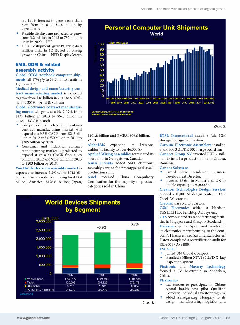
In addition to widespread economic doldrums in 1H’13, the electronic end markets changed. Apple lost some sales momentum, and as a result its suppliers suffered. Concurrently, personal computer demand declined (Chart 2) as media tablet and smartphones eroded PC sales (Chart 3).
The combined result of economic weakness and product uncertainty was a very weak 1Q’13 and a subdued seasonal
rebound in 2Q’13 with June 2013 electronic equipment shipments down 6% vs. June 2012 (Chart 4).
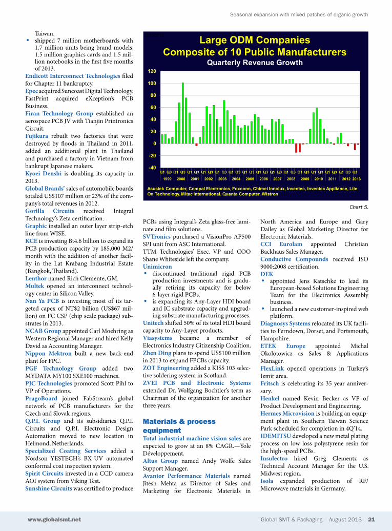
The traditional Taiwan-listed ODM companies (typically with China main-land manufacturing) felt the pain as their
combined quarterly sales “growth” has been negative since early 2012 (Chart 5).
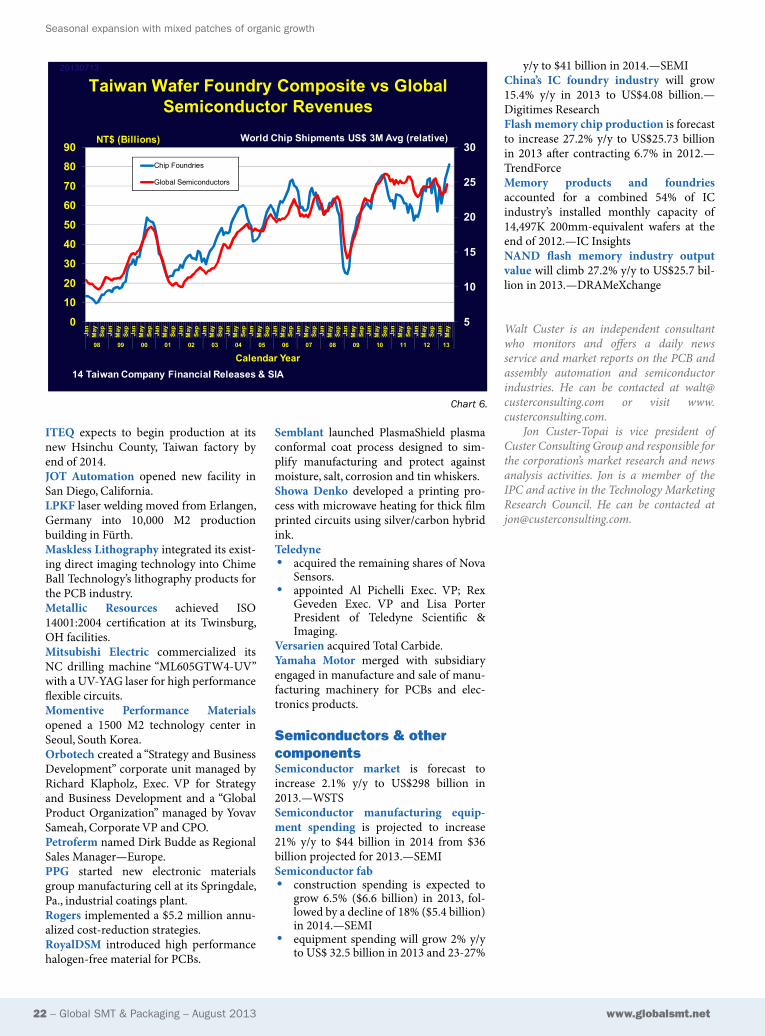
However, U.S. electronic equipment orders improved in May and Taiwan chip foundries (a leading indicator for global semiconductor shipments) reported a large jump in combined June revenues (Chart 6).
2013 will not be a banner year, but its second half looks more promising than its start!
end marketsGlobal IT spending will grow 2% y/y to US$3.72 trillion in 2013.—GartnerTaiwan tablet shipments will grow 24.5% y/y to 120 million units in 2013 even though global tablet demand is expected to grow 60-70% y/y to 230-240 million in 2013.—MICMobile Communications• Consumer wireless electronics sales
will increase by 54% y/y to 73 million units in 2013.—Strategy Analytics
• Mobile-cellular subscriptions will reach 6.8 billion by the end of 2013; 99 coun-tries already had more cell phones than people in 2011.—United Nations
• Global smart connected devices (PC, tablet and smartphone) shipments are expected to surpass 1.7 billion units by 2014 with roughly one billion units delivered to emerging markets.—IDC
• Smart connected devices in emerg-ing markets will surpass 1 billion units shipped by 2014 with more than 60% going to BRIC countries.—IDC
Datacom & Telecom• Data center network equipment rev-
enue declined 11% q/q to $2.3 billion in 1Q’13.—Infonetics Research
• Ethernet switch market increased 1% y/y to $4.7 billion worldwide in 1Q’13.—Infonetics Research
• Computers & Peripherals• PC shipments contracted 10.9% y/y to
76 million units in 2Q’13.—Gartner• PCs, tablets and mobile phones are
jointly projected to grow 5.9% to 2.35 billion units in 2013.—Gartner
• Storage• External disk storage systems factory
revenues declined 0.9% y/y to $5.9 bil-lion in 1Q’13.—IDC
Other• 3D printing revenue is projected to
grow from $1 billion in 2012 to $4 bil-lion by 2025.—IDTechEx
• Advanced automotive electronics
Walt Custer and Jon Custer-Topai
2013 will not be a banner year, but its second half looks more promising than its start!
Seasonal expansion with mixed patches
of organic growth
52.3
49.5
49.4
48.2
48.8
50.9
50.6
51.5
47.1
51.1
49.2
48.3
49.0
50.6
45.0 47.0 49.0 51.0 53.0 55.0
Japan
Taiwan
S Korea
China
Europe
USA
World
PMI
May June
Purchasing Managers' Indices May vs. June 2013
Markit Economics, JPMorgan and ISM
Above 50 = GrowthBelow 50 = Contraction
20130703
Chart 1.
Global SMT & Packaging – August 2013 – 19www.globalsmt.net
Seasonal expansion with mixed patches of organic growth
market is forecast to grow more than 50% from 2010 to $240 billion by 2020.—IHS
• Flexible displays are projected to grow from 3.2 million in 2013 to 792 million units in 2020.—IHS
• LCD TV shipments grew 4% y/y to 44.8 million units in 1Q’13, led by strong growth in China.—NPD DisplaySearch
ems, odm & related assembly activityGlobal ODM notebook computer ship-ments fell 17% y/y to 33.2 million units in 1Q’13.—IHSMedical design and manufacturing con-tract manufacturing market is expected to grow from $16 billion in 2012 to $34 bil-lion by 2019.—Frost & SullivanGlobal electronics contract manufactur-ing market will grow at a 9% CAGR from $435 billion in 2013 to $670 billion in 2018.—BCC Research• Computers and telecommunications
contract manufacturing market will expand at a 9.3% CAGR from $243 bil-lion in 2012 and $250 billion in 2013 to $389 billion by 2018.
• Consumer and industrial contract manufacturing market is projected to expand at an 8.9% CAGR from $128 billion in 2012 and $132 billion in 2013 to $203 billion by 2018.
Worldwide electronic assembly market is expected to increase 3.2% y/y to $742 bil-lion with Asia Pacific accounting for 413.9 billion; America, $126.6 billion; Japan,
$101.8 billion and EMEA, $96.6 billion.—ZVEIAlphaEMS expanded its Fremont, California facility to over 46,000 SF.Applied Wiring Assemblies terminated its operations in Georgetown, Canada.Asian Circuits added SMT electronic assembly service for prototype and small production runs.Assel received China Compulsory Certification for the majority of product categories sold in China.
BTSR International added a Juki ISM storage management system.Carolina Electronic Assemblers installed a Juki FX-3 XL/KE-3020 large board line.Connect Group NV invested EUR 2 mil-lion to install a production line in Oradea, Romania.Connor Solutions • named Steve Henderson Business
Development Director. • invested £3.6m in Sunderland, UK to
double capacity to 50,000 SF.Creation Technologies Design Services opened a 10,000 SF design center in Oak Creek, Wisconsin.Creonix was sold to Sparton.CSM Electronics added a Nordson YESTECH BX benchtop AOI system.CTS consolidated its manufacturing facili-ties in Singapore and Glasgow, Scotland.Darekon acquired Apelec and transferred its electronics manufacturing to the com-pany’s Haapavesi and Savonranta factories.Datest completed a recertification audit for ISO9001 / AS9100C.ESCATEC• joined UN Global Compact.• installed a Nikon XTV160 2.5D X-Ray
inspection system.Firstronic and Maxway Technology formed a JV, Maxtronic in Shenzhen, China.Flextronics • was chosen to participate in China’s
central bank’s new pilot Qualified Domestic Individual Investor program.
• added Zalaegerszeg, Hungary to its design, manufacturing, logistics and
Personal Computer Unit ShipmentsWorld
Gartner Dataquest 7/13 & prior reportsServer & Media Tablets not included
0102030405060708090
100
Q4 Q2 Q4 Q2 Q4 Q2 Q4 Q2 Q4 Q2 Q4 Q2 Q4 Q2 Q4 Q2 Q4 Q2 Q4 Q2 Q4 Q2 Q4 Q2 Q4 Q2 Q4 Q2 Q4 Q2
1999 2000 2001 2002 2003 2004 2005 2006 2007 2008 2009 2010 2011 20122013
Thou
sand
s
UnitsUnits (Millions)
Chart 2.
World Devices Shipments by Segment
Gartner 6/13
20130625
2012 2013 2014Mobile Phone 1,746,177 1,821,193 1,901,188Tablet 120,203 201,825 276,178Ultramobile 9,787 20,301 39,824PC (Desk & Notebook) 341,273 305,178 289,239
0
500,000
1,000,000
1,500,000
2,000,000
2,500,000
3,000,000+6.7%
Units (000)
+5.9%
Chart 3.

20 – Global SMT & Packaging – August 2013 www.globalsmt.net
Seasonal expansion with mixed patches of organic growth
service solutions relationship with Citrix.
• opened a Chengdu, China factory for plastic molding tools.
Foxconn/Hon Hai• set up a panel R&D center in Japan.• is increasing ‘robot army’ deployment
beyond its existing 20,000 factory robots.
• is adding an automated production base in Harbin, China.
• is investing NT$10 billion (US$332.9 million) to build a R&D facility and automated plants in Taichung, Taiwan.
• split off its connector unit into a sepa-rate entity.
GE opened a PCBA center in Minden, Nevada.GPV acquired Connectt.IEC Electronics regained NYSE listing compliance.Incap:• entered a PCBA manufacturing deal
with Tokheim, India.• sold its property in Vuokatti, Finland.International Manufacturing Services named Barry Black Marketing Manager.Jabil• acquired Nypro.• became primary global manufacturing
services and supply chain management provider for SGI.
• will consolidate operations and build a new HQ in Florida.
Kimball appointed Lonnie Nicholson as VP Business Analytics Kitron• named Dag Songedal interim CEO.• became EMS partner for DiaSorin’s
nucleic extraction instruments.LCL bought an i-Pulse M20 SMT place-ment machine.LEC installed a Speedprint SP700avi screen printer in Andalusia, Spain.MJS Designs added a SPEA 4060 dual sided flying probe system.OnCore Manufacturing named Walt Hussey COO.Plexus • opened a design center and manufac-
turing facility in Bathgate, Scotland. • named Ronnie Darroch, Regional
President—Plexus EMEA; Oliver Mihm, Sr VP—Global Engineering Solutions; Todd Kelsey, Exec. VP and COO and Steve Frisch, Exec. VP, global customer services.
QC Graphics • added Gary Tanel to its sales team.• implemented a real-time visual track-
ing system for managing PCBA and product routing.
Quanta began manufacturing more non-notebook products amid weaker notebook shipments and stronger competition in the tablet sector.Saline Lectronics purchased its fifth SMT line from Juki Automation Systems.Sanmina • became a contract manufacturer for
Haemonetics’ medical devices. • paid US$870,000 (RM2.61 mil-
lion) additional compensation to 856 Malaysian workers that were retrenched in October 2012.
Season Group acquired Outsource Electronics Limited.
Siix will spend 1 billion yen to build a Latin American plant in 2014.Sparton• acquired Creonix.• joined Russell 2000 Index.Syntech named John Harley as Sales Director.Texcel added a Takaya APT-9411 flying probe machine.Venne Electronics added a Synergy line with two Mydata MY100DXe14 machines.Wilson Process Systems invested £500,000 to increase its automatic board assembly capability.Wistron began production of non-intru-sive medical inspection instruments.
PcB fabricationAfrica’s PCB market is expected to grow 1.4% y/y to $619 million in 2013.—ZVEIChina’s average labor turnover for PCB manufacturers is currently between 6-8%.—H NakaharaEuropean PCB production has fallen from EUR 4.3 billion in 2001 to EUR 1.8 billion in 2012.—ZVEIGerman PCB market is estimated to grow 1.3% y/y to EUR 1.3 billion in 2013.—ZVEIA*STAR and Samsung Electronics devel-oped a fast and accurate way to estimate electromagnetic emissions from PCBs.APEX Thai is doubling its capacity with the addition of a new plant.Aspocomp wrote off approximately EUR 0.9 million of its former French subsid-iary’s bankruptcy-related provision for clo-sure expenses.AT&S • collaborated with EPCOS on develop-
ing technologies for embedding active and passive electronic components.
• Entered a JV with Intel for IC substrate cooperation.
Aurona Industries relocated 70-80% of its backup board production capacity in Kunshan, China to its newly built Taiwan plant to avoid tariffs.Bittele Electronics added quick-turn capabilities.Canon Components built a new PCB manufacturing plant in Thailand for 2-8 layer boards.Chin-Poon• is building a new plant in Taoyuan,
Taiwan.• sales of its auto boards account for 70%
of company’s total revenues.CMK Thailand is expanding its Thai oper-ations with HDI.Eagle Electronics added an Orbotech 8800 Hi LDI machine.Elitegroup Computer Systems• sold and leased back its HQ in Taipei,
World Electronic Equipment Monthly Shipments
Converted @ Constant 2010 Exchange Rates
Source: Custer Consulting Group
20130713
80
90
100
110120
130
140
150
160170
Jan
May
Sep
Jan
May
Sep
Jan
May
Sep
Jan
May
Sep
Jan
May
Sep
Jan
May
Sep
Jan
May
Sep
Jan
May
Sep
Jan
May
Sep
Jan
May
Sep
Jan
May
Sep
Jan
May
Sep
Jan
May
Sep
Jan
May
2000 2001 2002 2003 2004 2005 2006 2007 2008 2009 2010 2011 2012 2013
Thou
sand
s
June 2013 6% belowJune 2012
US$ B
Chart 4.
Global SMT & Packaging – August 2013 – 21www.globalsmt.net
Seasonal expansion with mixed patches of organic growth
Taiwan.• shipped 7 million motherboards with
1.7 million units being brand models, 1.5 million graphics cards and 1.5 mil-lion notebooks in the first five months of 2013.
Endicott Interconnect Technologies filed for Chapter 11 bankruptcy.Epec acquired Suncoast Digital Technology.FastPrint acquired eXception’s PCB Business.Firan Technology Group established an aerospace PCB JV with Tianjin Printronics Circuit.Fujikura rebuilt two factories that were destroyed by floods in Thailand in 2011, added an additional plant in Thailand and purchased a factory in Vietnam from bankrupt Japanese makers.Kyoei Denshi is doubling its capacity in 2013.Global Brands’ sales of automobile boards totaled US$107 million or 23% of the com-pany’s total revenues in 2012.Gorilla Circuits received Integral Technology’s Zeta certification.Graphic installed an outer layer strip-etch line from WISE.KCE is investing Bt4.6 billion to expand its PCB production capacity by 185,000 M2/month with the addition of another facil-ity in the Lat Krabang Industrial Estate (Bangkok, Thailand).Lenthor named Rich Clemente, GM.Multek opened an interconnect technol-ogy center in Silicon Valley.Nan Ya PCB is investing most of its tar-geted capex of NT$2 billion (US$67 mil-lion) on FC CSP (chip scale package) sub-strates in 2013.NCAB Group appointed Carl Moehring as Western Regional Manager and hired Kelly David as Accounting Manager.Nippon Mektron built a new back-end plant for FPC.PGF Technology Group added two MYDATA MY100 SXE100 machines.PJC Technologies promoted Scott Pihl to VP of Operations.PragoBoard joined FabStream’s global network of PCB manufacturers for the Czech and Slovak regions.Q.P.I. Group and its subsidiaries Q.P.I. Circuits and Q.P.I. Electronic Design Automation moved to new location in Helmond, Netherlands.Specialized Coating Services added a Nordson YESTECH’s BX-UV automated conformal coat inspection system.Spirit Circuits invested in a CCD camera AOI system from Viking Test.Sunshine Circuits was certified to produce
PCBs using Integral’s Zeta glass-free lami-nate and film solutions.SVTronics purchased a VisionPro AP500 SPI unit from ASC International.TTM Technologies’ Exec. VP and COO Shane Whiteside left the company.Unimicron• discontinued traditional rigid PCB
production investments and is gradu-ally retiring its capacity for below 6-layer rigid PCBs.
• is expanding its Any-Layer HDI board and IC substrate capacity and upgrad-ing substrate manufacturing processes.
Unitech shifted 50% of its total HDI board capacity to Any-Layer products.Viasystems became a member of Electronics Industry Citizenship Coalition.Zhen Ding plans to spend US$100 million in 2013 to expand FPCBs capacity.ZOT Engineering added a KISS 103 selec-tive soldering system in Scotland.ZVEI PCB and Electronic Systems extended Dr. Wolfgang Bochtler’s term as Chairman of the organization for another three years.
materials & process equipmentTotal industrial machine vision sales are expected to grow at an 8% CAGR.—Yole Développement.Altus Group named Andy Wolfe Sales Support Manager.Avantor Performance Materials named Jitesh Mehta as Director of Sales and Marketing for Electronic Materials in
North America and Europe and Gary Dailey as Global Marketing Director for Electronic Materials.CCI Eurolam appointed Christian Backhaus Sales Manager.Conductive Compounds received ISO 9000:2008 certification.DEK • appointed Jens Katschke to lead its
European-based Solutions Engineering Team for the Electronics Assembly business.
• launched a new customer-inspired web platform.
Diagnosys Systems relocated its UK facili-ties to Ferndown, Dorset, and Portsmouth, Hampshire.ETEK Europe appointed Michal Okolotowicz as Sales & Applications Manager.FlexLink opened operations in Turkey’s Izmir area.Fritsch is celebrating its 35 year anniver-sary.Henkel named Kevin Becker as VP of Product Development and Engineering.Hermes Microvision is building an equip-ment plant in Southern Taiwan Science Park scheduled for completion in 4Q’14.IDEMITSU developed a new metal plating process on low loss polystyrene resin for the high-speed PCBs.Insulectro hired Greg Clementz as Technical Account Manager for the U.S. Midwest region.Isola expanded production of RF/Microwave materials in Germany.
Large ODM Companies Composite of 10 Public Manufacturers
Quarterly Revenue Growth
Asustek Computer, Compal Electronics, Foxconn, Chimei Innolux, Inventec, Inventec Appliance, Lite On Technology, Mitac International, Quanta Computer, Wistron
20130713
-40
-20
0
20
40
60
80
100
120
Q1 Q3 Q1 Q3 Q1 Q3 Q1 Q3 Q1 Q3 Q1 Q3 Q1 Q3 Q1 Q3 Q1 Q3 Q1 Q3 Q1 Q3 Q1 Q3 Q1 Q3 Q1 Q3 Q1
1999 2000 2001 2002 2003 2004 2005 2006 2007 2008 2009 2010 2011 2012 2013
Chart 5.
22 – Global SMT & Packaging – August 2013 www.globalsmt.net
Seasonal expansion with mixed patches of organic growth
ITEQ expects to begin production at its new Hsinchu County, Taiwan factory by end of 2014.JOT Automation opened new facility in San Diego, California.LPKF laser welding moved from Erlangen, Germany into 10,000 M2 production building in Fürth.Maskless Lithography integrated its exist-ing direct imaging technology into Chime Ball Technology’s lithography products for the PCB industry.Metallic Resources achieved ISO 14001:2004 certification at its Twinsburg, OH facilities.Mitsubishi Electric commercialized its NC drilling machine “ML605GTW4-UV” with a UV-YAG laser for high performance flexible circuits.Momentive Performance Materials opened a 1500 M2 technology center in Seoul, South Korea.Orbotech created a “Strategy and Business Development” corporate unit managed by Richard Klapholz, Exec. VP for Strategy and Business Development and a “Global Product Organization” managed by Yovav Sameah, Corporate VP and CPO.Petroferm named Dirk Budde as Regional Sales Manager—Europe.PPG started new electronic materials group manufacturing cell at its Springdale, Pa., industrial coatings plant.Rogers implemented a $5.2 million annu-alized cost-reduction strategies.RoyalDSM introduced high performance halogen-free material for PCBs.
Semblant launched PlasmaShield plasma conformal coat process designed to sim-plify manufacturing and protect against moisture, salt, corrosion and tin whiskers.Showa Denko developed a printing pro-cess with microwave heating for thick film printed circuits using silver/carbon hybrid ink.Teledyne • acquired the remaining shares of Nova
Sensors.• appointed Al Pichelli Exec. VP; Rex
Geveden Exec. VP and Lisa Porter President of Teledyne Scientific & Imaging.
Versarien acquired Total Carbide.Yamaha Motor merged with subsidiary engaged in manufacture and sale of manu-facturing machinery for PCBs and elec-tronics products.
semiconductors & other componentsSemiconductor market is forecast to increase 2.1% y/y to US$298 billion in 2013.—WSTSSemiconductor manufacturing equip-ment spending is projected to increase 21% y/y to $44 billion in 2014 from $36 billion projected for 2013.—SEMISemiconductor fab • construction spending is expected to
grow 6.5% ($6.6 billion) in 2013, fol-lowed by a decline of 18% ($5.4 billion) in 2014.—SEMI
• equipment spending will grow 2% y/y to US$ 32.5 billion in 2013 and 23-27%
y/y to $41 billion in 2014.—SEMIChina’s IC foundry industry will grow 15.4% y/y in 2013 to US$4.08 billion.—Digitimes ResearchFlash memory chip production is forecast to increase 27.2% y/y to US$25.73 billion in 2013 after contracting 6.7% in 2012.—TrendForceMemory products and foundries accounted for a combined 54% of IC industry’s installed monthly capacity of 14,497K 200mm-equivalent wafers at the end of 2012.—IC InsightsNAND flash memory industry output value will climb 27.2% y/y to US$25.7 bil-lion in 2013.—DRAMeXchange
Walt Custer is an independent consultant who monitors and offers a daily news service and market reports on the PCB and assembly automation and semiconductor industries. He can be contacted at [email protected] or visit www.custerconsulting.com.
Jon Custer-Topai is vice president of Custer Consulting Group and responsible for the corporation’s market research and news analysis activities. Jon is a member of the IPC and active in the Technology Marketing Research Council. He can be contacted at [email protected].
Taiwan Wafer Foundry Composite vs Global Semiconductor Revenues
14 Taiwan Company Financial Releases & SIA
20130713
5
10
15
20
25
30
0
10
20
30
40
50
60
70
80
90
Jan
May
Sep
Jan
May
Sep
Jan
May
Sep
Jan
May
Sep
Jan
May
Sep
Jan
May
Sep
Jan
May
Sep
Jan
May
Sep
Jan
May
Sep
Jan
May
Sep
Jan
May
Sep
Jan
May
Sep
Jan
May
Sep
Jan
May
Sep
Jan
May
Sep
Jan
May
98 99 00 01 02 03 04 05 06 07 08 09 10 11 12 13
Chip Foundries
Global Semiconductors
NT$ (Billions)
Calendar Year
World Chip Shipments US$ 3M Avg (relative)
Chart 6.

24 – Global SMT & Packaging – August 2013 www.globalsmt.net
JPCA, Japan & the industry: The Show Must Go on
The show must go on! But what show? There were more than 60 small booths representing universi-
ties and local institutes at the JPCA Show in Tokyo in June, filling spots formerly inhabited by PCB makers and their suppli-ers. Few Westerners (other than exhibitors or employees of Japanese or Asian-owned companies) could be seen. There were displays of 2.5D and 3D packages, but no affordable solutions. Embedded compo-nents were still on many minds, especially with the knowledge that they are used in camera sensors. Embedded actives still await the implementation of “known good die” at the wafer level. Now let’s see, on boards of about an 1/8 of a square inch each, 100 million cameras would need about 12.5 million square feet of PCBs, less than the output of one of the larger HDI fabricator plants in China. One has to wonder if these will be replaced by organic CMOS sensors some day soon.
Printed electronic circuits are still seeking their niche markets. Many of the vaunted bare board equipment displayed were slight retreads of systems already shown elsewhere in the world. Ushio appeared to be one of the exceptions with its new direct imaging system with a 5 µm line and space capability. A display of the
“intestines” of smart phones showed that they have migrated away from their prede-cessors. Flexible circuits seemed to be lim-ited to use for connecting the touch screen. Main boards sported 10 layers of FR-4 and ALIVH type of construction. AT&S’ booth promoted 2.5D packaging on the heels of its stated intent of producing IC substrates, while Unimicron budgeted $325 million to develop thinner high density chip scale substrates.
In general, shop owners and equip-ment suppliers to the bare board industry that attended the JPCA event were rather morose in their outlooks. Increased “ratio-nalization” is expected. The merger of Sony and Juki’s SMT equipment businesses sparked further speculation. Conflict with China over the small, uninhabited Senkaku-Diaoyu Islands have put a damper on Japan’s current trade and agreements as well as possibilities for future growth
in electronic (and other) manufactur-ing. Optimists that hoped for a 2nd half pick-up had their spirits dampened a bit with news of continued slowing growth in China. —I still have a problem understand-ing why economists are complaining about growth of GNP that is “only” about 7%.
The relative lack of innovation on dis-play, the decline of the PCB industry in Japan, and future opportunities were the
dinner topics for the “old timers” on June 6. Shifting from mass production to short run niche market demands will not fill the gap left by behemoth automated opera-tions designed for very large runs. Moving into printed electronics must await stan-dards development and growth in market demand.
But there was a glimmer of hope when the rapid rise of display panels was brought up. Demand is multiplying for handhelds, large tabletop systems, automotive systems, and other displays. Shipments of touch screen panels are forecasted to increase to 2.8 billion units in 2016. Some of the tech-nology is related or similar (but different)
to board substrate fabrication: coating of ITO onto glass, processing of glass, depos-iting of films and conductors, imaging, applying protective coatings,
The topic of graphene was introduced by dessert, but time ran out. It should be interesting to hear what one of the IPC’s keynoters has to say about this one at the TMRC (Technology Market Research Conference) gathering of senior managers and executives in September.
There surely must be some opportuni-ties for those with vision and creative tal-ents.
The 11th China (Shenzhen) International Touch Screen Exhibition 2013 will be held November 25-27. The 2014 JPCA Show will take place June 4-6, 2014, at Tokyo Big Sight.
Gene Weiner, president of Weiner International Associates, is an IPC Hall of Fame Inductee and has been voted one of the The 10 Most Influential Persons in the PCB Industry.
JPcA, Japan & the Industry: The Show
Must Go on Gene Weiner
Shifting from mass production to short run niche market demands will not fill the gap left by behemoth automated operations designed for very large runs.
Global SMT & Packaging – August 2013 – 25www.globalsmt.net
Fan-in QFn packages fitting an expanding number of applications
overviewQFN, or quad flat pack no lead, packages are a more recent package introduction than the more established packages such as the SO, but they have quickly attained popularity. The QFN is in the chip scale package (CSP) category, being close to die sized. It has leads on four sides of the package, which are encapsulated within the mold compound so that the package rides flat on the printed circuit board (PCB). The lack of visible leads protruding from the bottom gives rise to the term “no lead” in this package name.
The DFN, or dual flat pack no lead, package is similar, but with leads on just two sides of the package. The QFN has the advantage of having the ability to reach higher I/O counts, and thus can accommo-date a greater number of devices.
The QFN was developed in 2002 and came onto the market in 2003. It was origi-nally called a depopulated small outline no lead (SON) in JEDEC terms. In 2012, nearly 12.4 percent of all ICs were packaged in QFNs. QFNs are expected to increase to more than 14.8 percent of all ICs by 2017.
QFNs currently house a large number of devices; the largest markets include standard logic, voltage regulators and ref-erences, amplifiers and comparators, con-sumer analog, computer analog, and com-munications analog, and special-purpose logic chips.
Robust and relatively cheap and easy to assemble, this package is ideal for applica-tions such as simple logic and analog. With the leadframe totally encapsulated within the mold compound (with the exception of the ends of the bond pads), the package has reduced parasitics, making it ideal for RF applications. These packages offer less
inductance than substrate packages due to fewer material layers for the electron to pass through. Because the leads do not extend beyond the mold compound, this package also has less inductance than other leadframe packages, a result of the electron not needing to make the transition from encapsulation within the mold compound to beyond the mold compound on the open leadframe foot. The electron travels on the surface of the leadframe.
The shortened lead length increases the speed of devices, as the electron does not travel quite as far to reach the PCB from the die. The entire leadframe is reduced in size due to the closely cropped nature of the package in relation to the die, and to the shortened lead length, which does not have the external gullwing leads.
The QFN offers thermal performance superior to that of leaded packages of simi-lar body size and I/O count. The leadframe is on the bottom of the package; thus the die attach pad is exposed, allowing it to be easily soldered directly to the board, and allowing heat to dissipate into the PCB. Heat transfers faster into solid material than into ambient.
The shipping medium does not have to be expensive, as bent leads during shipping of the package are not an issue. However, being flat on the board means that the board cannot have extraneous material beneath the package or the bond pads will not reach the board. The clearance beneath the package that is common in the other
leadframe-type packages does not exist or is considerably shortened for QFN packages.
extending the lead count—the fan-in QfN
To further increase the reach of this package, the latest development in QFN packages is to extend the number of rows of leads from the usual one to two or three rows of leads. The leadframe is stamped or etched as in any other leadframe solution, but the leads are of various lengths, either two or three different lengths. When bent downward for connection to the PCB by trim and form equipment, the result is a multi-row, array-patterned package solution with a hole in the center, or fan-in QFN. This allows the number of package leads to extend into the hundreds, up from generally fewer than 50. The resulting package is a high-density, leadframe array package.
The fan-in QFN can have two or three rows of leads. Over time there will be a larger variety of applications for this pack-age, including both those with a higher I/O count and those with a lower I/O count. Overall, the average I/O count will increase with time.
The fan-in QFN has the ability to cap-ture the lower end of the QFP (quad flat pack) market. This includes extending its reach to higher bit MCUs and both logic and analog communications chips, largely bound for RF handheld gadgets that require a small-form-factor package.
Products housed in fan-in QFN pack-ages will include 8- and 16-bit MCUs, spe-cial-purpose logic computer chips, logic and analog communications chips, low-
Continued on page 27
“Robust and relatively cheap and easy to assemble, the QFN package is ideal for applications such as simple logic and analog.”
fan-in QfN packages fitting an
expanding number of applications
Sandra L. Winkler
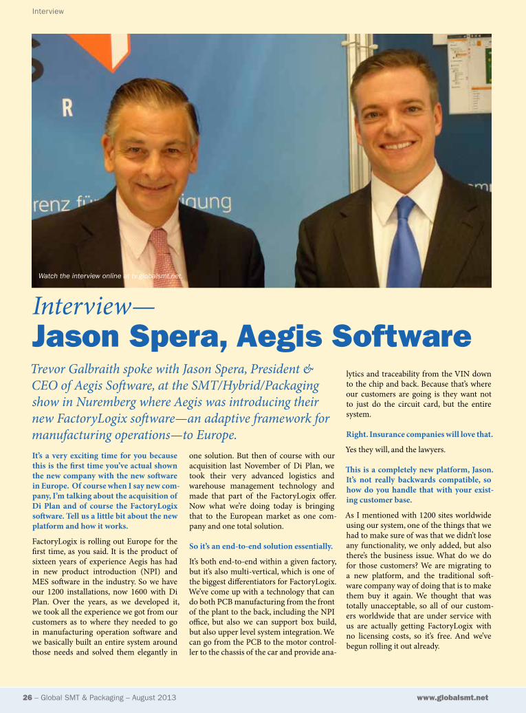
Title
26 – Global SMT & Packaging – August 2013 www.globalsmt.net
Watch the interview online at tv.globalsmt.net.
It’s a very exciting time for you because this is the first time you’ve actual shown the new company with the new software in Europe. Of course when I say new com-pany, I’m talking about the acquisition of Di Plan and of course the FactoryLogix software. Tell us a little bit about the new platform and how it works.
FactoryLogix is rolling out Europe for the first time, as you said. It is the product of sixteen years of experience Aegis has had in new product introduction (NPI) and MES software in the industry. So we have our 1200 installations, now 1600 with Di Plan. Over the years, as we developed it, we took all the experience we got from our customers as to where they needed to go in manufacturing operation software and we basically built an entire system around those needs and solved them elegantly in
one solution. But then of course with our acquisition last November of Di Plan, we took their very advanced logistics and warehouse management technology and made that part of the FactoryLogix offer. Now what we’re doing today is bringing that to the European market as one com-pany and one total solution.
So it’s an end-to-end solution essentially.
It’s both end-to-end within a given factory, but it’s also multi-vertical, which is one of the biggest differentiators for FactoryLogix. We’ve come up with a technology that can do both PCB manufacturing from the front of the plant to the back, including the NPI office, but also we can support box build, but also upper level system integration. We can go from the PCB to the motor control-ler to the chassis of the car and provide ana-
lytics and traceability from the VIN down to the chip and back. Because that’s where our customers are going is they want not to just do the circuit card, but the entire system.
Right. Insurance companies will love that.
Yes they will, and the lawyers.
This is a completely new platform, Jason. It’s not really backwards compatible, so how do you handle that with your exist-ing customer base.
As I mentioned with 1200 sites worldwide using our system, one of the things that we had to make sure of was that we didn’t lose any functionality, we only added, but also there’s the business issue. What do we do for those customers? We are migrating to a new platform, and the traditional soft-ware company way of doing that is to make them buy it again. We thought that was totally unacceptable, so all of our custom-ers worldwide that are under service with us are actually getting FactoryLogix with no licensing costs, so it’s free. And we’ve begun rolling it out already.
Interview—
Trevor Galbraith spoke with Jason Spera, President & CEO of Aegis Software, at the SMT/Hybrid/Packaging show in Nuremberg where Aegis was introducing their new FactoryLogix software—an adaptive framework for manufacturing operations—to Europe.
interview
Jason Spera, Aegis Software

Global SMT & Packaging – August 2013 – 27www.globalsmt.net
Title
That’s impressive. You’ve got a couple of areas in there, for example, RMA. Can we talk about that, it’s the handling of the return of materials basically.
Yes, there are two major things we handle. As I mentioned, you hear from your cus-tomers over sixteen years, and there are two challenges in the market. One is RMA, where a unit has a life cycle beyond its original manufacture. It goes to the field, and then it returns sometimes because either it’s defective or it needs to be field upgraded. It’s difficult for an MES system to have that life cycle of being produced, exiting, coming back to be changed, going back into the field, and so on. FactoryLogix fundamentally handles there in an unlim-ited number of returns and back out to the field, which is very important when you start doing analytics about your overall performance, not just in-factory quality, but what is your actual yield in the field, and how much work are you doing and the costs of that. We can handle all of that now.
That’s pretty powerful. That really is. The other thing I think that it also handles is customization.
We call it “configure to order.” It’s been a giant challenge in the industry for people who have it. “Configure to order,” put most simply, is like when you buy a Dell laptop and you choose a solid-state drive versus the standard, different memory. When you’re doing these online orders, you’re generating a singular, unique unit. Getting an MES system to adapt the process and production to all those permutations is a very difficult challenge. It’s been solved in the past by custom software built typically by the OEM. We’ve come up with a way
of handling that within a standard MES system. We can literally handle configure-to-order without engineering customiza-tion on our part or an integrator. It actually fundamentally handles it. So for compa-nies that need that, it’s actually a tremen-dous step forward.
I can imagine, especially here in Germany, that would be particularly powerful, because so much customization happens over here.
Product configurations, all the unique…yes.
Thank you for giving us a very, very broad overview of FactoryLogix. I’m sure we’re going to delve into deeper parts of it as we go forward, but for now, Jason, thank you very much for joining us.
—Trevor Galbraith
If you want more information on FactoryLogix, visit the Aegis website at www.aiscorp.com
interview
cost baseband, HDMI, buffers, and server clocks. Future applications will also include storage controllers. Because this package has the ability to attain higher I/O counts at a lower cost than substrate-based packages, it will soon be utilized in a wide assortment of products.
The forecastTraditional QFNs will have a compound annual growth rate (CAGR) of 9.3 per-cent for units, and 9.7 percent for revenue through 2017. This is higher than the global worldwide IC package CAGR of 5.5 percent for units and 5.2 percent for rev-enue through 2017. The subset of fan-in QFNs will have a CAGR of 38.6 percent CAGR for units, and 27.1 percent for rev-enue through 2016. The fan-in QFNs addi-tionally will experience the growth rate
shown in Table 1.More information on this topic and
more can be found in New Venture Research’s Advanced IC Packaging Markets, Materials, and Technologies, 2012 Edition. For information on how to obtain this report, please contact Karen Williams at [email protected], Tel: (408) 244-1100.
Sandra Winkler is the senior analyst for IC packaging at New Venture Research Corp (formerly Electronic Trend Publications). She began her analyst career as an indepen-dent consultant to the telecommunications industry nearly 20 years ago.
Since 1995, Ms. Winkler has authored all of ETP/NVR widely cited reports on IC packaging. She has spoken at numerous industry conferences and is a contributing editor for Chip Scale Review magazine.
“The fan-in QFN has the ability to reach to higher bit MCUs and both logic and analog communications chips, largely bound for RF handheld gadgets that require a small-form-factor package.”
2012 2013 2014 2015 2016
Growth rate 184.5% 15.4% 25.9% 11.9% 10.5%
As a Percentage of Total QFn Market
3.3% 3.4% 3.7% 3.8% 3.7%
Table 1. Growth rate of fan-in QFNs.
fan-in QfN packages fitting an expanding number of applications—Continued from page 35
“We thought that was totally unacceptable, so all of our customers worldwide that are under service with us are actually getting FactoryLogix with no licensing costs.”

28 – Global SMT & Packaging – August 2013 www.globalsmt.net
you cannot pass or fail hAlT
The use of the term ‘Highly Accelerated Life Testing,’ better known as HALT, originated in the late 1980’s within
two different sectors of the electronics industry.
Munikoti and Dhar of Nortel originally used the term HALT in 1987 to describe a solution to the accelerated life tests being performed at that time on ceramic capaci-tors. However, the far more popular use of the term began in 1988 (based on various marketing literature) by Gregg Hobbs of Hobbs Engineering. Though the mindset and the process goes back several decades, Hobbs used the term to describe a sequen-tial process of applying a variety of stresses to a product, either individually or in com-bination, to identify the weak links in the design.
Over time, HALT has evolved to describe a specific set of tests (hot step stress, cold step stress, vibration step stress, thermal cycling, combined) performed in a specific environmental test chamber (thermal cycling chamber with adjustable nozzles over a repetitive shaker (RS) vibra-tion table) at a specific point in the product development process (right after first pro-totype).
HALT can play a very crucial role in ensuring a robust design early in the design process and establishing constraints before certain aspects of the design are fixed. However, success of HALT is can be very dependent upon a complimentary activity, root-cause analysis (RCA), because you cannot pass or fail HALT. A true HALT is the process of learning about the weak points of your design and determining what steps are necessary and sufficient to improve those limitations. Without the knowledge provided by root-cause inves-tigation of HALT failures, that is what failed and why, the value of HALT is greatly reduced.
A great example of the value of RCA and HALT can be seen in a case study of a HALT performed on an industrial power supply. The industrial power supply in question had an operating temperature range of 5˚C to 50˚C and a storage tem-perature range of -40˚C to 65˚C.
Cold step stress testing
During cold step stress testing the units experienced a variety of failure modes• At -30˚C, the liquid crystal display
(LCD) refresh rates slowed. Refresh speed returned to normal when rechecked within operational range of 5˚C/50˚C
• At -40˚C, refresh rate stopped on LCD. Refresh speed returned to normal when rechecked within operational range of 5˚C/50˚C
• At -50˚C, LCD failed to illuminate (non-recoverable failure)The failure modes described above
are well known for LCDs and are due to material transitions within the liquid crys-tal. The LCD manufacturer specified an operational range of -20˚C to 70˚C and the displays operated as intended within that temperature range, which is approxi-mately 20˚C beyond the operating range. The bigger concern is the permanent fail-ure at -50˚C. This offers only a 10˚C margin over the storage temperature and is not an expected failure mode for LCD’s. The loss of illumination suggests an issue with the LED backlight. A likely failure mode is a hardening of the silicone potting around the LED, causing separation of one or more wire bond connections.
hot step stress testingDuring hot step stress testing, the unit shut down at +110C and did not recover. Post-test failure analysis of Unit 2 identified the failure site as a DC/DC converter. The operating range of the DC/DC Converter is given as -25˚C to 90˚C. The permanent failure was surprising as recoverable fail-ures typically occur at least 20˚C below the temperature of permanent failure. This would indicate two possible scenarios. The first is that the DC/DC Converter experi-enced some type of recoverable failure that was not detectable by monitoring during HALT. This scenario is concerning as it suggests that there is no margin beyond the specification on this DC/DC converter. The alternative scenario is that this DC/DC Converter only experienced permanent failure.
In both scenarios, the failure tempera-
ture, whether around 90˚C or at 110˚C, is at least 40˚C above the operating specifica-tion of 50˚C. Considering the temperature difference between the operating specifi-cation and the failure temperature, there are two options. The first is to do nothing because sufficient margin was present. The second is to consider the DC/DC converter the weakest component and to determine if this may indicate a potential future risk.
rapid thermal transitions testingDuring rapid thermal cycling, the power supply experienced a sticky relay. Intermittent failures should be taken very seriously whenever detected during prod-uct qualification. “Sticky” relays are often an indication of micro-welding, potentially due to timing issues or excessive current. In some manner, rapid thermal transitions may have aggravated the component or the circuit sufficiently to trigger this event, potentially indicating insufficient margin or robustness.
Vibration step stress testingSeveral failures occurred during vibration step stress testing, including:• At 10 Grms, three LEDs broke off• At 15 Grms, a ground screw loosened• At 40 Grms, horizontal lines were noted
in the LCD and bleeder resistors broke offOne of the most important questions
in assessing the results of a HALT test is determining its relevancy. Since the oper-ating environment of the industrial power supply is not expected to see vibration, the vibration step stress test is to some extent assessing the robustness of the design during shipping and transportation. Therefore, an appropriate root-cause evalu-ation must be based upon an understand-ing of the actual loads seen during shipping and transportation.
Three available Power Spectral Density (PSD) profiles for shipping are shown in Figure 1, Table 1 and Figure 2. [Note: This function, although it is called “power…”, is not its unit of measurement. This term is used because very frequently the square of
You cannot pass or fail hALT
Craig Hillman
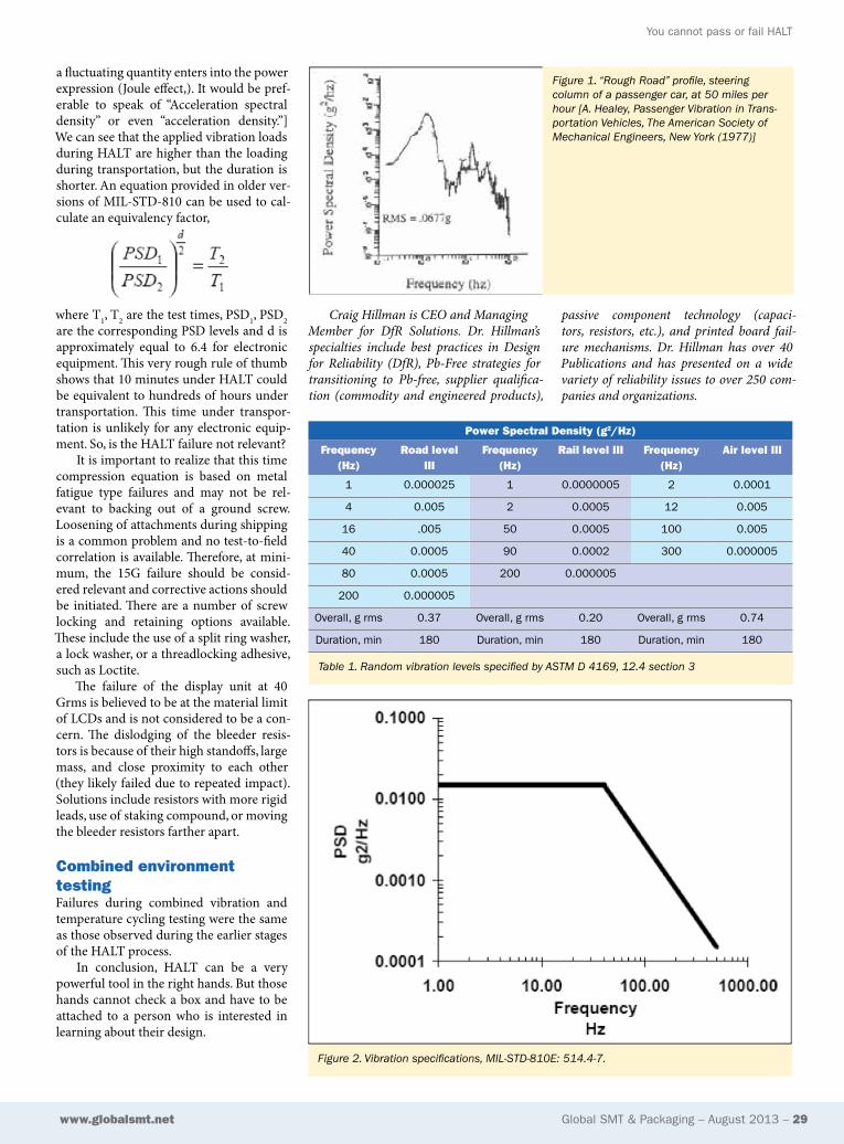
Global SMT & Packaging – August 2013 – 29www.globalsmt.net
you cannot pass or fail hAlT
a fluctuating quantity enters into the power expression (Joule effect,). It would be pref-erable to speak of “Acceleration spectral density” or even “acceleration density.”] We can see that the applied vibration loads during HALT are higher than the loading during transportation, but the duration is shorter. An equation provided in older ver-sions of MIL-STD-810 can be used to cal-culate an equivalency factor,
where T1, T2 are the test times, PSD1, PSD2 are the corresponding PSD levels and d is approximately equal to 6.4 for electronic equipment. This very rough rule of thumb shows that 10 minutes under HALT could be equivalent to hundreds of hours under transportation. This time under transpor-tation is unlikely for any electronic equip-ment. So, is the HALT failure not relevant?
It is important to realize that this time compression equation is based on metal fatigue type failures and may not be rel-evant to backing out of a ground screw. Loosening of attachments during shipping is a common problem and no test-to-field correlation is available. Therefore, at mini-mum, the 15G failure should be consid-ered relevant and corrective actions should be initiated. There are a number of screw locking and retaining options available. These include the use of a split ring washer, a lock washer, or a threadlocking adhesive, such as Loctite.
The failure of the display unit at 40 Grms is believed to be at the material limit of LCDs and is not considered to be a con-cern. The dislodging of the bleeder resis-tors is because of their high standoffs, large mass, and close proximity to each other (they likely failed due to repeated impact). Solutions include resistors with more rigid leads, use of staking compound, or moving the bleeder resistors farther apart.
combined environment testingFailures during combined vibration and temperature cycling testing were the same as those observed during the earlier stages of the HALT process.
In conclusion, HALT can be a very powerful tool in the right hands. But those hands cannot check a box and have to be attached to a person who is interested in learning about their design.
Craig Hillman is CEO and Managing Member for DfR Solutions. Dr. Hillman’s specialties include best practices in Design for Reliability (DfR), Pb-Free strategies for transitioning to Pb-free, supplier qualifica-tion (commodity and engineered products),
passive component technology (capaci-tors, resistors, etc.), and printed board fail-ure mechanisms. Dr. Hillman has over 40 Publications and has presented on a wide variety of reliability issues to over 250 com-panies and organizations.
Power spectral density (g2/hz)
frequency (Hz)
road level III
frequency (Hz)
rail level III frequency (Hz)
Air level III
1 0.000025 1 0.0000005 2 0.0001
4 0.005 2 0.0005 12 0.005
16 .005 50 0.0005 100 0.005
40 0.0005 90 0.0002 300 0.000005
80 0.0005 200 0.000005
200 0.000005
overall, g rms 0.37 overall, g rms 0.20 overall, g rms 0.74
Duration, min 180 Duration, min 180 Duration, min 180
Table 1. Random vibration levels specified by ASTM D 4169, 12.4 section 3
Figure 1. “Rough Road” profile, steering column of a passenger car, at 50 miles per hour [A. Healey, Passenger Vibration in Trans-portation Vehicles, The American Society of Mechanical Engineers, New York (1977)]
Figure 2. Vibration specifications, MIL-STD-810E: 514.4-7.
30 – Global SMT & Packaging – August 2013 www.globalsmt.net
off shoring, on shoring—not suring?
A long time ago a “wise” man said Go East and your manufacturing costs will disappear!
Many heeded this omen, rushing head-long to embrace the “new message.” This took several forms: those already using sub-contractors simply switched their orders to the new lands on a promise of a utopian future. Some closed down their in-house manufacturing and moved their whole pro-duction to a third party in these “new lands.” This was a real “leap of faith” and sometimes had dire consequences. The third way was to open a facility in a “low cost” region and use existing management and control sys-tems, but with lower costs. This potentially produced the least gain but was the safest option. The company I worked for set up a manufacturing unit in China using this option in the year 2000, with a purpose-built factory and a faithful duplication of our quality and management systems. The existing manufacturing site in the UK was also retained; this gave us a huge increase in capacity and the ability to win business at lower prices. It worked so well that after a few years a large player bought the business from us to give them a strong base in Asia. So we are proof that this strategy can work. I won’t say there were no hiccups, but it was a success, both financially and in terms of
quality of product. We still maintain a facil-ity there to build x-ray systems for Asia; this also works very well.
But there were many stories of disasters, many as the plan had not been thought through fully. If you move your manufac-turing to a place which is five weeks away by sea, your time to market will increase. If you work in different time zones with different languages, your communica-tions will not be easy. If you work with a company whose manufacturing standards are lower than yours, you will have quality issues. If your boards require final set up or programming at your site, it will add time to the process, as will final QA there before sending to customers.
But the bigger issues which appeared were those of choosing the correct partner. Some medium and small sizes companies joined the exodus in the hope of huge sav-ings, some without thinking things through well enough. This led to tie ups with unsuit-able partners, some far too big to really be focused on small volumes, some used to building commercial quality products, not the higher quality required. Some even set things up by finding a partner on the web and never even visiting. This did not end well in most cases.
Off shoring works very well, but the
product and the partnership has to be right. High volume mobiles, tablets, etc., need a low-cost manufacturing base, but it also has to produce good quality and high technology products. It is not unusual for competitors to share manufacturers for this kind of product, and the volumes are almost too big to comprehend. If you are a low to mid volume company with a quality product and a need to respond to market changes by changing your order patterns, then “going East” is probably not for you. But some have made this work well. By working really hard on finding the right partner and growing a strong partnership, they have formed a good solution to the low cost-good quality conundrum.
The recently hyped move to on shor-ing is also an interesting phenomenon; it is viewed by many as the pull back to the
“old plan” as off shoring failed! It is no such thing, or at least it should not be. Many companies have realised that as the time to market required to maintain sales has reduced, and the need for flexibility in the manufacturing chain increases, then the long shipping times become an issue. Add to this that in many markets product life-cycles are also reducing dramatically, and the need for closer ties and faster responses from manufacturing become critical to
Keith Bryant
off shoring, on shoring—not suring?
effi cient production managementHighlight Segment 2013
messe münchen
november 12 – 15, 2013
www.productronica.com
20th international trade fair for
innovative electronics production
more informationwww.productronica.com/en/2013
p13-Abdul_203x275-GlobalSMT&Pack_E.indd 1 11.07.13 15:12

effi cient production managementHighlight Segment 2013
messe münchen
november 12 – 15, 2013
www.productronica.com
20th international trade fair for
innovative electronics production
more informationwww.productronica.com/en/2013
p13-Abdul_203x275-GlobalSMT&Pack_E.indd 1 11.07.13 15:12

32 – Global SMT & Packaging – August 2013 www.globalsmt.net
off shoring, on shoring—not suring?
growth and sometimes even survival. So do they open up their moth-balled manu-facturing plants? Go back to the same sup-plier they dumped ages ago? Well I am sure some do, but it is not a rational solution, even if the option still exists.
The answer is what it has been all along, even before the off shoring rush was thought about! Build the product in the best place; do not be swayed by “the next great thing” or “the competition is doing it!” Simply look at your product, volumes, time needed to market and all the other key points and make the best decision for manufacturing.
When you are in the West it can be nice when you read headlines that a certain company or other is setting up manufac-turing back in your country and moving production back from the East. But the important thing is to have your manu-facturing done where it is best suited to the needs of your product. I see many companies moving back to, or expanding their facilities, in low cost regions closer to their end customers: Romania, Mexico and Turkey, to name just three. This can be
a good solution: similar time zones, fewer language issues, and a short supply chain. Some CEMs are making strategic moves to open facilities close to potential custom-ers in an effort to strengthen their market share, Defence being a good example of a sector where this is happening. Some OEMs are starting to work with partners in country as they need more flexibility and control than even regionalisation can supply. Yes, “Regionalisation is the new Globalisation!”
So what does the future hold? I believe in a more enlightened view on where things are made: all of the above options are right for some people. It is a matter of finding the partner in the place which you believe will work best, then investing time and effort in the relationship; this is what really brings the results. Working at arms’ length from your suppliers is not a good way forward; you have to engage and involve them in as much as you can. I talk to many companies that involve their key suppliers at the development stage, when board size and layout can be changed to improve yield and reduce costs. This is the
real answer to low cost manufacturing. You should engage with the experts in each key area where cost can be saved and listen to them. Low-cost manufacture can only be achieved by doing this. And it is true whichever country you choose to make it in: poor design is still the biggest hurdle to efficient manufacture and test, so perhaps your biggest issue with cost of manufac-ture can be fixed without moving too far!
Every company is much more com-petitive than it was a few years ago; yields and quality have been improved by better equipment and new technologies; and investment in quality has been the biggest spend for most companies in the last few years. Thankfully we work in a changing environment, and mostly for the better.
international diary4-6 September 2013productronica IndiaNew Delhi, Indiaproductronica-india.com
4-6 September 2013SEMICON TaiwanTaipei, Taiwansemicontaiwan.org
29 September-3 October 2013IMAPS Intl Symposium MicroelectronicsOrlando, Florida, USAimaps2013.org
8-10 October 2013SEMICON EuropeDresden, Germanysemiconeuropa.org
10-12 October 2013NEPCON VietnamHanoi, Vietnamnepconvietnam.com
15-16 October 2013SMTA InternationalFort Worth, Texas, USAsmta.org/smtai
4-7 November 2013Int’l Wafer Level Packaging Conference San Jose, California, USAiwlpc.com
12-15 November 2013productronicaMunich, Germanyproductronica.com
20-21 November 2013Printed Electronics USASanta Clara, California, USAprintedelectronicsusa.com
15-17 January 2014INTERNEPCON JapanTokyo, Japaninternepcon.jp/en/
12-14 Feburary 2014SEMICON Korea Seoul, Koreasemiconkorea.org
18-20 March 2014productronica ChinaShanghai, Chinae-p-china.com

High Speed Wide Range Placer for the Next Decade
Fresh Energy in Your Business
Main OfficeSamsungtechwin R&D Center, 701, Sampyeong-dong, Bundang-gu, Sungnam-Si, Gyeonggi-Do, 463-400, Korea• Tel : +82-70-7147-5459, 6309 Fax : +82-31-8018-3723• http : // www.samsung-smt.com
Exhibition Place Date
Shenzhen China 2013. 8.27(Tue) ~ 29(Thu)
Taiwan 2013. 9. 4(Wed) ~ 6(Fri)
203x275.indd 1 13. 07. 12 오후 7:40