the future of hdi via structures, power delivery, and ...viasystems.com the future of hdi via...
TRANSCRIPT
The Future of HDI Via Structures, Power
Delivery, and Thermal Management in Next
Generation Printed Circuits
Presented By
Tom Buck
Solutions without Boundaries

Use or disclosure of information contained on this page is subject to the restriction on page 2 of this document
∂
Copyright T-Buck Viasystems 2014
2
Notice:
Notification of Proprietary Information: This document
contains proprietary information of Viasystems Corp. and
its receipt or possession does not convey any rights to
reproduce or disclose its contents, or to manufacture,
use, or sell anything it may describe. Reproduction,
dissemination, disclosure, or use, in whole or in part,
without specific written authorization of Viasystems. is
strictly forbidden. All data contained within this
document are subject to this restriction.

Use or disclosure of information contained on this page is subject to the restriction on page 2 of this document
∂
Copyright T-Buck Viasystems 2014
Presentation Objectives
Today’s advanced electronic systems require a complex
blend of many process technologies that must work in
concert to provide interconnect solutions ranging from
high current DC to millimeter wave radar…
…The goal of this presentation is to examine
emerging PCB technologies and their impact on
next generation electronic systems
• Laser drilled microvia’s
• Stacked microvia’s
• Blind & Buried vias
• Thermal management techniques
• Heavy copper design
• Embedded busbar technologies
• Precision etching technologies
77 GHz Antenna
High current
embedded bus-bar

Use or disclosure of information contained on this page is subject to the restriction on page 2 of this document
∂
Copyright T-Buck Viasystems 2014
Today’s Agenda
• Market drivers & what’s driving PCB densities
• Alternate via structures and microvia’s
• NextGenTM Mass terminated microvia
• Thermal management techniques
• High current busbar and heavy copper
• Precision etching technology for RF and Microwave
• Summary and wrap up

Use or disclosure of information contained on this page is subject to the restriction on page 2 of this document
∂
Copyright T-Buck Viasystems 2014
Overview
PCB Market Drivers
&
What’s Driving PCB Densities ?

Use or disclosure of information contained on this page is subject to the restriction on page 2 of this document
∂
Copyright T-Buck Viasystems 2014
0.50 mm XeTel
1.27 mm
XeTel
BGA
PCB
1.27 mm BGA package
Localized via density
62/cm2 (400/in.2)
0.50 mm BGA package
Localized via density
400/cm2 (2580/in.2)
Silicon Die
6.45 x Increase
in via density
0.20 mm
Density Trends In Array Packages
0.20 mm Flip Chip
Localized via density
2500/cm2 (16,129/in.2)
6.25 x Increase
in via density
BGA
PCB
Increasing I/O Density Chip Scale Packaging Flip Chip Packaging

Use or disclosure of information contained on this page is subject to the restriction on page 2 of this document
∂
Copyright T-Buck Viasystems 2014
Increasing Densities in Array Packages
357 I/O BGA Package
Common BGA Pin pitch:
1.27 mm
1.0 mm
0.8 mm
0.75 mm
0.65 mm
0.5 mm
Silicon die encased
in molded plastic Interposer substrate to
transform Silicon geometries
to PCB geometries. Most
often made with PCB process
0.4 mm
0.25 mm
Through hole PCB
Drilled hole diameter and
Pitch are reaching limits
and restricting routing

Use or disclosure of information contained on this page is subject to the restriction on page 2 of this document
∂
Copyright T-Buck Viasystems 2014
Circuit Density & Mechanical Drilling limitations
Drill dia.
Pad dia.
Line width
Max Thk. *
Hole density
Channel
12 mils
25 mils
5 mils
125 mils
400/in.
40 in./in.^2
10 mils
20 mils
3.5 mils
100 mils
625/in.
50 in./in.^2
8 mils *
18 mils
3.5 mils
62 mils
1008/in.
31 in./in.^2
Decreasing Channel Density Increasing $ Technology Shift
1.27 mm 1.0 mm 0.8 mm 0.5 mm
6 mils *
16 mils
N/A
32 mils
2580/in.
Escape Only !
• Board thickness limited by drill flute length
• Hole barrel reliability with lead free assembly Standard Production

Use or disclosure of information contained on this page is subject to the restriction on page 2 of this document
∂
Copyright T-Buck Viasystems 2014
Mechanical Drilling
• Alignment issues
• Drill wander
• Drill life
• Hole quality
Same process smaller drills !
CNC PCB Drilling Machine

Use or disclosure of information contained on this page is subject to the restriction on page 2 of this document
∂
Copyright T-Buck Viasystems 2014
Putting Small Diameter Drills Into Perspective
Carbide drill bit
5.9 mil (150 micron)
Human hair
2.5 mil (60 micron) to
3.5 mil (90 micron) • Small diameter are very fragile
• High speed spindles are required
• Feed rates are about 50% of standard
via diameters
• Drill life of 300 to 600 hits depending
on material
• Short flute length limits hole depth
• Drill cost is higher
• Limited availability from offshore PCB
production

Use or disclosure of information contained on this page is subject to the restriction on page 2 of this document
∂
Copyright T-Buck Viasystems 2014
Array Pattern Escape: Through Hole IPC Class 2
1.27 mm: 3 Track 1.0 mm: 2 Track
0.8 mm: 1 Track 0.5 mm: 0 Track
10 mil drill
20 mil pad
4 mil track
10 mil drill
20 mil pad
4 mil track
8 mil drill
18 mil pad
3.5 mil track
6 mil drill
14 mil pad
No routing
What now ?

Use or disclosure of information contained on this page is subject to the restriction on page 2 of this document
∂
Copyright T-Buck Viasystems 2014
Laser Drilling Technology
YAG-CO2
Combination ND:YAG CO2
Forms holes by removing copper with the ND:YAG laser
and the dielectric and re-enforcing material with the CO2
laser (Approximately 3,500 to 13,000 holes per minute)
Laser drilled Microvia
Layer 1 to 2
0.005”
0.006”
0.0
03” Termination or “Capture Pad”
Typical Via Diameter
Note: 1- Hole depth is limited by plating aspect
ratio(depth/diameter) Typical aspect ratio on laser drilled
holes is 0.5:1 to 0.6:1 max
2- Holes greater than 0.005” are generally considered
too large to be placed in component pad

Use or disclosure of information contained on this page is subject to the restriction on page 2 of this document
∂
Copyright T-Buck Viasystems 2014
Array Pattern Routing: Microvia
1.0 mm: 3 Track 0.8 mm: 2 Track
0.5 mm: 1 Track 0.4 mm: 0 Track
5 mil Laser
10 mil pad
4 mil track
5 mil Laser
10 mil pad
4 mil track
5 mil Laser
10 mil pad
3 mil track
5 mil Laser
10 mil pad
No track Routing is possible with smaller internal pads and sub 3 mil
lines reducing yields
What now ?

Use or disclosure of information contained on this page is subject to the restriction on page 2 of this document
∂
Copyright T-Buck Viasystems 2014
4 mil microvia/8.66 mil pad
2.36 mil trace/2.36 mil space
on plated layers
0.4 mm BGA Escape: Fine Line Approach
Advanced Routing (60/60/220)

Use or disclosure of information contained on this page is subject to the restriction on page 2 of this document
∂
Copyright T-Buck Viasystems 2014
Routing By Via Row Reduction
Q1
Q2
Q4
Q3
100 I/O Array 0.4 mm
L1
L2
L3
L4
L5
L6
Once routing channels are eliminated by current
process limitations, each row of the array pattern
will require a unique routing layer. As each row is
connected it will open routing for the next.
This approach dramatically
Increases PCB complexity !

Use or disclosure of information contained on this page is subject to the restriction on page 2 of this document
∂
Copyright T-Buck Viasystems 2014
Stacked MicroVia (SMV®)
L1-L2, L1-L3 & L1-L4
Second Generation Microvia Geometries
Stacked MicroVia Landing on a
Plated & Non-Plated Layer

Use or disclosure of information contained on this page is subject to the restriction on page 2 of this document
∂
Copyright T-Buck Viasystems 2014
Overview
Achieving Higher Densities
Using
Alternate Via Structures

Use or disclosure of information contained on this page is subject to the restriction on page 2 of this document
∂
Copyright T-Buck Viasystems 2014
Is Advanced PCB Technology Cost Effective ?
Increasing Density
Incre
asin
g C
ost
Technology Shift
Yield Reduction Non Optimized
Classic Technology Utilization Curves
Cost Effective
Region
Through Hole PCB
Technology
“Bad Engineering”
Crossover
point
Crossover
point
Microvia PCB
Technology NextGen PCB
Technology
All technologies have finite limitations ! As applications approach
Limits, technologies can become ineffective.
“Process Limits”

Use or disclosure of information contained on this page is subject to the restriction on page 2 of this document
∂
Copyright T-Buck Viasystems 2014
Technology Options Extending PCB Densities
Through Hole PCB
Technology Limits ?
• Via-In-Pad technologies
• Blind via (sequential Lamination)
• Blind and Buried via (sequential Lamination)
• Controlled depth drilling
• Laser Microvia
• Stacked Microvia
• Laser modified controlled depth drill
• NextGenTM
Technology Options:
• Mechanical drill size
• Plating aspect ratio
• PTH reliability
• Minimum line width
• Layer count > thickness
• High speed via transitions
Many options will require
Enhanced registration &
Copper plating capabilities

Use or disclosure of information contained on this page is subject to the restriction on page 2 of this document
∂
Copyright T-Buck Viasystems 2014
Controlled Depth
Mechanically Drilled Hole
Prepreg
Prepreg
Prepreg
Core
Prepreg
Core
• Increased channel density on layers below the controlled depth drill
• Standard PTH geometry apply, Depth limited by aspect ratio
• No sequential lamination required
Core
Via Structures: Mechanical Controlled Depth Drill
Drilled
Through
Hole

Use or disclosure of information contained on this page is subject to the restriction on page 2 of this document
∂
Copyright T-Buck Viasystems 2014
Laser Modified Controlled
Depth Hole
Prepreg
Prepreg
Prepreg
Core
Prepreg
Core
Via Structures: Laser Modified Controlled Depth
• Increased channel density on layers below the controlled depth drill
• Allows a connection with no stub
• Standard PTH geometry apply, Depth limited by aspect ratio
• No sequential lamination required
Core
Via hole is first mechanically drilled then with a
laser the remaining dielectric is removed
clearing a path to the copper layer
Drilled
Through
Hole

Use or disclosure of information contained on this page is subject to the restriction on page 2 of this document
∂
Copyright T-Buck Viasystems 2014
Mechanically
Drilled Blind
Prepreg
Prepreg
Prepreg
Prepreg
Core
Prepreg
Core
Bond layer between
upper and lower sub
Sub Lam.
Sub Lam.
Via Structures: Blind Via
• Increased channel density on lower sub lamination
• Standard PTH geometry apply, reduced aspect ratio on sub drill
• Anti-pad diameter must account for tolerance buildup in multiple laminating cycles
Drilled
Through
Hole
Use or disclosure of information contained on this page is subject to the restriction on page 2 of this document
∂
Copyright T-Buck Viasystems 2014
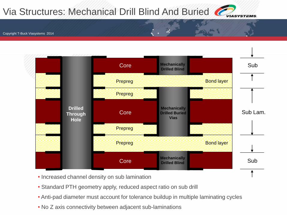
Sub
Sub Lam.
• Increased channel density on sub lamination
• Standard PTH geometry apply, reduced aspect ratio on sub drill
• Anti-pad diameter must account for tolerance buildup in multiple laminating cycles
• No Z axis connectivity between adjacent sub-laminations
Mechanically
Drilled Buried
Vias
Prepreg
Core
Prepreg
Prepreg
Prepreg
Core
Core
Mechanically
Drilled Blind
Mechanically
Drilled Blind Sub
Bond layer
Bond layer
Via Structures: Mechanical Drill Blind And Buried
Drilled
Through
Hole

Use or disclosure of information contained on this page is subject to the restriction on page 2 of this document
∂
Copyright T-Buck Viasystems 2014
• Increased channel density on layer 1 and 2 from reduced geometry
• Increased channel density on layers n-1 to n resulting from a blind hole
• Standard PTH geometry apply to mechanical drilled holes
• Dielectric thickness layer 1:2 limited by plating aspect ratio (0.5:1 to 0.6:1)
Laser drilled via
Prepreg
Core
Prepreg
Prepreg
Prepreg
Core
Core
Mechanical
drilled hole
Via Structure: Laser Microvia
Drilled
Through
Hole

Use or disclosure of information contained on this page is subject to the restriction on page 2 of this document
∂
Copyright T-Buck Viasystems 2014
• Increased channel density on layer 1 and 2 from reduced geometry
• Increased channel density on layers n-1 to n resulting from a blind hole
• Standard PTH geometry apply to mechanical drilled holes
• Dielectric thickness layer 1:2 limited by plating aspect ratio (0.5:1 to 0.6:1)
Laser drilled via
Prepreg
Prepreg
Core
Core
Prepreg
Prepreg
Prepreg
Mechanical
drilled hole
Buried via
Via Structure: Microvia & Blind Mechanical Sub
Drilled
Through
Hole

Use or disclosure of information contained on this page is subject to the restriction on page 2 of this document
∂
Copyright T-Buck Viasystems 2014
Overview
Increasing Density Using
Stacked Microvia’s and it’s
Implications ?
Use or disclosure of information contained on this page is subject to the restriction on page 2 of this document
∂
Copyright T-Buck Viasystems 2014
First and Second Generation Microvia Structures
1:2 mVia 1:3 mVia 1:3 Stacked
plate fill mVia
1:2 Plate
fill mVia
1:2 2:3
Staircase mVia
2-4-2 HDI Substrate
4 Layer
MLB core
HDI Dielectric 2 Layer HDI
buildup
First Generation
Microvia Structures Second Generation
Microvia Structures

Use or disclosure of information contained on this page is subject to the restriction on page 2 of this document
∂
Copyright T-Buck Viasystems 2014
Second Generation Microvia: Solid Copper
Bottom-up filling behavior is attributed to
the action of organic additives (must be
controlled to prescribed limits)
Suppressor rapidly forms current inhibiting
film on Cu surface. Film has little
geometric dependence due to high
suppressor solution concentration
Accelerated bottom-up fill behavior is due to
a local accumulation of brightener species
at the feature base
As surface area is reduced during
deposition, the concentration of brightener
species increases, resulting in a non-
equilibrium surface concentration. This local
concentration of brightener accelerates the
plating rate relative to the surface.
Source:
Mechanism of via filling
Brightener
Carrier
Planar Microvia
Stacked Microvia
0.010”
0.004” dia.
Capture pad
Layer 1
Layer 2
Layer 3
0.002”
Preferred fill Method !

Use or disclosure of information contained on this page is subject to the restriction on page 2 of this document
∂
Copyright T-Buck Viasystems 2014
Cu Foil
Layer 1
Land pad
H2
Cu Plating
Example 1: Two layer stacked microvia
(+2) terminating on a copper foil shown
with a copper plat fill on the layer 1 to
layer 2 via for via-in-pad application. H1
and H2 represent the dielectric thickness
between layers and standard design
rules apply.
Cu Foil
Cu Plating
Cu Foil
H1
Layer 2
Capture pad
Cu Foil
H2
Cu Plating
Cu Foil
Cu Plating
Cu Foil
H1
Cu Foil
Example 2: Two layer stacked microvia
(+2) terminating on a plated layer. This
example illustrates how the internal solid
copper via’s become the building block for
the via’s on top until you get to the layer 1
to 2 via. The final 1 to 2 via has the option
to be filled with copper (recommended for
via-in-pad) or they can be left as a
standard via with a divot if used as an
interstitial via. H1 and H2 represent the
dielectric thickness between the layers
where standard microvia rules apply.
Layer 1
Layer 2
Layer 3
Layer3
Capture pad
Stacked Microvia Examples
Second Generation Microvia Geometries:
Use or disclosure of information contained on this page is subject to the restriction on page 2 of this document
∂
Copyright T-Buck Viasystems 2014
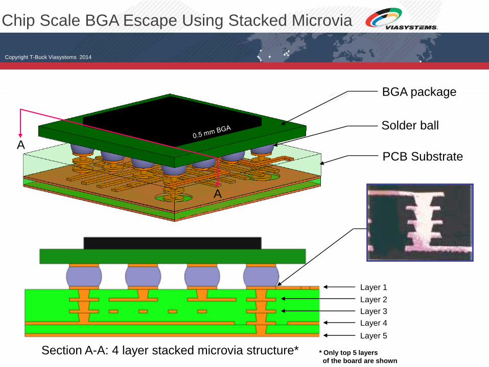
Chip Scale BGA Escape Using Stacked Microvia
A
A
Section A-A: 4 layer stacked microvia structure* * Only top 5 layers
of the board are shown
Layer 1
Layer 2
Layer 3
Layer 4
Layer 5
BGA package
Solder ball
PCB Substrate

Use or disclosure of information contained on this page is subject to the restriction on page 2 of this document
∂
Copyright T-Buck Viasystems 2014
Next Generation - SMV™ Technology
• Viasystems continues to drive technology enhancements in the SMV™ arena:
– Requires one to two lamination cycle (based on design constraint), reducing fabrication
time
– Eliminates plating cycle of inner layers
– Improves inner layer characteristics, signal integrity and electrical characteristics
– Reduces demand on plating and lamination, improving facility capacity utilization
– Allows for thinner finished product
– Initial customer builds have been encouraging with significant early interest
– This is a Viasystems patented technology
Viasystems is constantly working to
enable new technologies to meet the
needs of high-technology customer
demands with small, feature rich products
(ex. mobile phones, PDA, cameras, and
other such products).
Use or disclosure of information contained on this page is subject to the restriction on page 2 of this document
∂
Copyright T-Buck Viasystems 2014
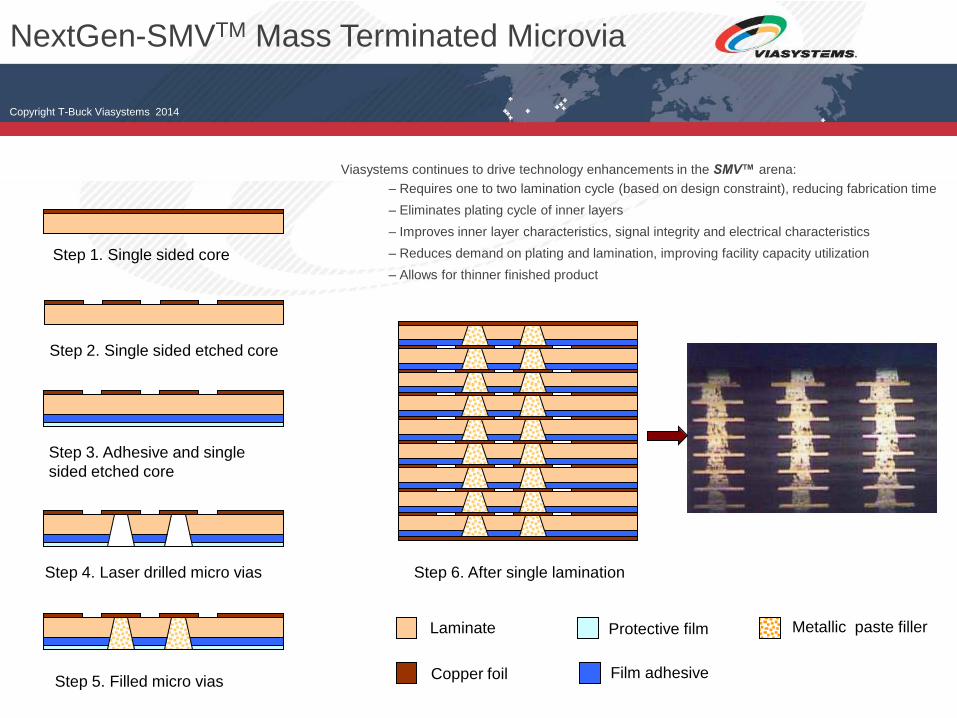
NextGen-SMVTM Mass Terminated Microvia
Step 1. Single sided core
Step 2. Single sided etched core
Step 3. Adhesive and single
sided etched core
Step 4. Laser drilled micro vias
Step 5. Filled micro vias
Step 6. After single lamination
Laminate
Copper foil Film adhesive
Protective film Metallic paste filler
Viasystems continues to drive technology enhancements in the SMV™ arena:
– Requires one to two lamination cycle (based on design constraint), reducing fabrication time
– Eliminates plating cycle of inner layers
– Improves inner layer characteristics, signal integrity and electrical characteristics
– Reduces demand on plating and lamination, improving facility capacity utilization
– Allows for thinner finished product

Use or disclosure of information contained on this page is subject to the restriction on page 2 of this document
∂
Copyright T-Buck Viasystems 2014
Triacid Chemclean LDI Resist Coat LDI ExposeDevelop, Etch,
StripAlternate Oxide
HRL/CSL
AdhesivePEP
Laser Via
GenerationVia Fill
Layup and
Laminate
LDI Resist Coat LDI Expose Develop Alternate OxideLayup and
LaminateDrill LDI Tooling
Laser Via
GenerationSMV Deburr SMV Electroless
Photoprint Dots Develop Dots Plate Microfill Resist Strip Planarize B/B Electroless LDI Resist Coat
Pattern Plate
CopperSolder Plate Resist Strip Etch Solder Strip
Repeat for
Sub 4 to 7
Repeat for
Sub 3 to 8
Repeat for
Sub 2 to 9
Repeat for
Sub 1 to 10
Soldermask, Final
Finish,Legend, Fab
Soldermask, Final
Finish,Legend, Fab
Material Issue
Material Issue
Pumice Scrub LDI Resist Coat LDI ExposeDevelop, Etch,
StripLaser LDI Tooling
Single Lamination
Stacked Via
Sequential Lamination
Stacked Via
MJT 2/14/2007
NextGen
Conventional
Single Lamination Parallel Process (SLPP™)
NextGen-SMV™ vs. Conventional SMV™

Use or disclosure of information contained on this page is subject to the restriction on page 2 of this document
∂
Copyright T-Buck Viasystems 2014
HDI-Link™ - Sub-to-Core Attach
Potential solution to add multiple HDI layers to a buried via, ex. 3+N+3
Final Drill / Finishes
DDi HDI-Link™, Sub-to-core attach
Patent Pending
Buried Via = N layers

Use or disclosure of information contained on this page is subject to the restriction on page 2 of this document
∂
Copyright T-Buck Viasystems 2014
35 Multiple Standard multi layer
subs after Lamination Process
Sub-Link™ - Sub-to-Sub Attach (Sub A,B,C,…)
Solution for High Aspect Ratio PCB, > 33:1 AR
Patent Pending
Sub-Link™, Sub-to-Sub Attach
SUB A
SUB B
SUB C

Use or disclosure of information contained on this page is subject to the restriction on page 2 of this document
∂
Copyright T-Buck Viasystems 2014
Overview
Advanced Thermal Management
Techniques

Use or disclosure of information contained on this page is subject to the restriction on page 2 of this document
∂
Copyright T-Buck Viasystems 2014
37
Thermal Conduction In PCB’s
Die
IC Package
Lead / Balls
Printed Circuit
Enclosure / Rack
Environment
Heat Flow Thermal resistance at each
level of an electronic system
will impact conduction…
…Heat generated
must go somewhere !
Relative surface area
Use or disclosure of information contained on this page is subject to the restriction on page 2 of this document
∂
Copyright T-Buck Viasystems 2014
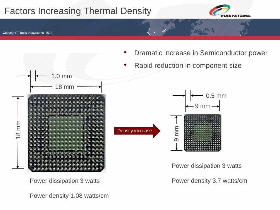
18 mm
1.0 mm
18 m
m
9 mm
0.5 mm
9 m
m
Power dissipation 3 watts
Power density 1.08 watts/cm
Power dissipation 3 watts
Power density 3.7 watts/cm
Density increase
Factors Increasing Thermal Density
• Dramatic increase in Semiconductor power
• Rapid reduction in component size

Use or disclosure of information contained on this page is subject to the restriction on page 2 of this document
∂
Copyright T-Buck Viasystems 2014
39
0
50
100
150
200
250
300
350
400
450
Copper
Silv
er
Gold
Nicke
l
Alu
min
um
Sold
er
Sta
blcor
FR-4
Cer
amic
CB-1
00
TC35
0
RO43
50
Thermal Conductivity
Thermal conductivities of common PCB materials
Watt/m
. K
0.3 W/m . K 1.0 W/m . K
0.64 W/m . K ST10: 10 W/m . K

Use or disclosure of information contained on this page is subject to the restriction on page 2 of this document
∂
Copyright T-Buck Viasystems 2014
40
Glass Fabric
Copper foil
Epoxy resin
Anisotropic PCB Thermal Conductivities
K II
K
PCB’s are composed of resin,
glass and a random distribution
of copper that is parallel to the
PCB surface. An approximate
value for parallel and perpendicular
conductivity are:
K II = 27.5 W/mK
K = 0.41 W/mK
Approximations are based on FR4 based laminate and will vary
based on actual board construction and specific distribution of
copper ! But they are a good starting point.

Use or disclosure of information contained on this page is subject to the restriction on page 2 of this document
∂
Copyright T-Buck Viasystems 2014
41
PCB Thermal Resistance: Parallel
Component (Heat Source)
1.0 cm (0.394”)
Heat flow through the PCB
Example:
PCB 15.25 mm x 22.9 mm
(6” x 9”)
R II = L
K * A =
11.45E-3
27.5 * 1.6E-3 * 15.25E-3 = 17.06 K/W
The example does not take into account the thermal resistance
from the IC and perpendicular resistance in the PCB
Note: This example assumes
Z axis conductivity

Use or disclosure of information contained on this page is subject to the restriction on page 2 of this document
∂
Copyright T-Buck Viasystems 2014
42
Component (Heat Source)
1.0 cm (0.394”)
PCB R^ approximately
0.41 W/mK
PCB Thermal Resistance: Perpendicular
Example:
PCB 15.25 mm x 22.9 mm
(6” x 9”)
R ^ =
L
K * A =
1.6E-3
0.41 * (10E-3)2 = 39 K/W
Relatively large thermal resistance in the Z axis since copper
layers are separated by high resistance laminate
Note: This example only accounts for
the conductivity of the substrate
in the Z axis

Use or disclosure of information contained on this page is subject to the restriction on page 2 of this document
∂
Copyright T-Buck Viasystems 2014
43
Thermal Limitations Of Dielectric Materials
Common dielectric materials have relatively low thermal
conductivities where as electrical conductors have
relatively high conductivities…
… Increased thermal conductivity is
achieved with conductors
Hot Side
Cold Side
Dielectric materials
0.3 to 1.0 W/mK Electrical conductors
25 to 400 W/mK
Heat Flow
Low
Flow
High
Flow

Use or disclosure of information contained on this page is subject to the restriction on page 2 of this document
∂
Copyright T-Buck Viasystems 2014
44
Thermal Via Applications
Plated through hole provide a
thermal shunt resistance bypassing
the dielectric layer
Issues: Through holes will wick solder away
from the component connection and deposit
on the back side of the board !
Thermal pad for conducting
head from the component to
internal planes or external heat
sink on the back of the board

Use or disclosure of information contained on this page is subject to the restriction on page 2 of this document
∂
Copyright T-Buck Viasystems 2014
45
Number of thermal via’s
Thermal
resistance
K/W
Thermal Resistance: Parallel Thermal Via’s
Note: Thermal via’s placed in a 1.0 cm (0.0394) square

Use or disclosure of information contained on this page is subject to the restriction on page 2 of this document
∂
Copyright T-Buck Viasystems 2014
46
Methods To Increase Thermal Via Conductivity
0.001” 0.001” 0.002”
Standard Conductive Filled Thicker Copper
Common thermal via constructions: Copper = 380 W / m K
Conductive filler =3.5 to 6.7 W /m K

Use or disclosure of information contained on this page is subject to the restriction on page 2 of this document
∂
Copyright T-Buck Viasystems 2014
47
Thermal Resistance vs Via Technologies
Thermal via length in mm
Thermal
resistance
K/W
Use or disclosure of information contained on this page is subject to the restriction on page 2 of this document
∂
Copyright T-Buck Viasystems 2014
48
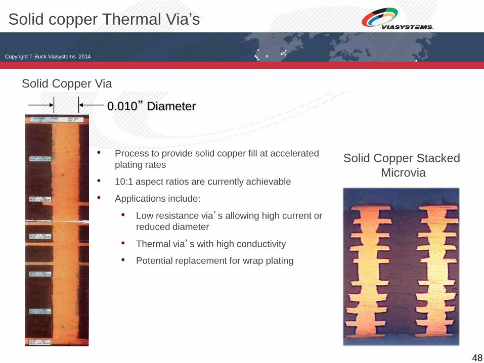
Solid copper Thermal Via’s
0.010” Diameter
Solid Copper Via
• Process to provide solid copper fill at accelerated
plating rates
• 10:1 aspect ratios are currently achievable
• Applications include:
• Low resistance via’s allowing high current or
reduced diameter
• Thermal via’s with high conductivity
• Potential replacement for wrap plating
Solid Copper Stacked
Microvia

Use or disclosure of information contained on this page is subject to the restriction on page 2 of this document
∂
Copyright T-Buck Viasystems 2014
49
Thermal Resistance Parallel Via’s
Number of thermal via’s
Thermal
resistance
K/W
Note: Thermal via’s placed in a 1.0 cm (0.0394) square
Both have the same
relative thermal
conductivity

Use or disclosure of information contained on this page is subject to the restriction on page 2 of this document
∂
Copyright T-Buck Viasystems 2014
50
Thermal Management
Bonded Heat Sinks
• Thermal via-farms
• Heat-transfer underneath component through the PCB to spread heat to
inner layer copper-planes and / or opposite side of PCB where external heat
sink or housing.

Use or disclosure of information contained on this page is subject to the restriction on page 2 of this document
∂
Copyright T-Buck Viasystems 2014
Thermal Management
Aluminum and Copper Heat
sinks post-attached to finished
PCBs using Pressure
Sensitive Adhesive Tapes.
Pre cut pressure sensitive adhesive Machined heat sink
Bare Board Composite assembly

Use or disclosure of information contained on this page is subject to the restriction on page 2 of this document
∂
Copyright T-Buck Viasystems 2014
Thermal Management
Embedded Copper Coins
• Press Fit Coin (PFC) (Inlay)
• Cu coins are mechanically “Press Fit” or “Inlayed” into the PCB during manufacture.
• Good for applications requiring improved thermal heat transfer over traditional via-farms.
• Coin shape can be designed for almost any application
• Automotive – Round coins (hot spot cooling), drilled openings offer tighter size control
• PA devices – Rectangle coins offer customized coin options while still maintaining good coin
retention
PFC
Inlay

Use or disclosure of information contained on this page is subject to the restriction on page 2 of this document
∂
Copyright T-Buck Viasystems 2014
53
Thermal Management
Thermal Conductivity: via-farm vs
solid copper embedded coins
Thermal resistance through
the board =1.3 K/W
Thermal resistance through
the board = 0.05 K/W
Copper coin

Use or disclosure of information contained on this page is subject to the restriction on page 2 of this document
∂
Copyright T-Buck Viasystems 2014
Thermal Management
•Embedded Copper
• Similar in configuration to press fit, these copper
coins are inserted during the lamination process
• The coin is retained in the coin opening by the resin
of the PCB material and thus becomes an integral
part of the PCB
• Can be drilled and plated as part of the of PCB
• Similar applications as press fit with good thermal
heat transfer
Post Coin Bonding
Embedded
PCB cross-section PCB Bottom view PCB Top-view

Use or disclosure of information contained on this page is subject to the restriction on page 2 of this document
∂
Copyright T-Buck Viasystems 2014
Thermal Management
• E-Coin (Viasystems Patented)
• Cu flanged coins are inserted during the
lamination process becoming an integral part of the
PCB
• Excellent coin to PCB grounding capabilities
• Applications where both electrical (grounding) and
thermal requirements are needed.
• Excellent planarity of coin to PCB surface
Post Coin Bonding
E-Coin

Use or disclosure of information contained on this page is subject to the restriction on page 2 of this document
∂
Copyright T-Buck Viasystems 2014
56
Thermal Management
Surface Attached Copper Coin
• Sweat Solder
• Post coin attach of pallet and coin heat sinks utilizing solder attach as the bond system
• Post coin/pallet attach utilizing thermally/electrically conductive adhesive
• Copper/Au plated coins attached after PCB build completion
Post Coin Bonding
Sweat Solder

Use or disclosure of information contained on this page is subject to the restriction on page 2 of this document
∂
Copyright T-Buck Viasystems 2014
Overview
Integrated High Current
Applications
&
Thermal Planes

Use or disclosure of information contained on this page is subject to the restriction on page 2 of this document
∂
Copyright T-Buck Viasystems 2014
Heavy Copper Outer-layers
External conductors. Copper-plate & Etch technology • If solder mask coverage is required (min 5um), the max. total copper thickness is 210um (6Oz)
• Special solder mask ink and process (E-Spray) is recommended to reduce risk on solder mask-
cracking.
• Due to copper thickness and CTE mismatch solder mask cracking during Thermal Cycling can not be
avoided.
• PCB design (copper and solder mask) have huge impact on cracking of solder mask.
• For critical applications we recommend to use extreme heavy copper only on inner-layers.
20
140
8.3 mils (210um) final copper thickness on external layers 58

Use or disclosure of information contained on this page is subject to the restriction on page 2 of this document
∂
Copyright T-Buck Viasystems 2014
Heavy Copper Outer-layers
• External conductors. Copper-plate & Etch technology
• Copper Layout has influence on cracks in solder mask.
• Sharp corner in copper create stress-points increasing risk on solder
mask cracks.
Good; rounded corners in copper pattern Not Good; sharp corners in copper pattern
59
Design recommendations

Use or disclosure of information contained on this page is subject to the restriction on page 2 of this document
∂
Copyright T-Buck Viasystems 2014
Solder Mask Design Recommendations
• Solder mask design;
– Solder mask design has influence on cracking.
– Sharp corner in solder mask-design create stress-points increasing
risk on solder mask cracks.
60

Use or disclosure of information contained on this page is subject to the restriction on page 2 of this document
∂
Copyright T-Buck Viasystems 2014
Solder mask & Gap Filler for 12 Oz Outer Layer
Challenge: Solder Mask coverage & thickness at trace corner
Resolution: Gap Filler filling by stencil screen printing
61
Etched 12 oz
Outer layer
Polymer filling
Of the etched gap
Planar surface after solder mask

Use or disclosure of information contained on this page is subject to the restriction on page 2 of this document
∂
Copyright T-Buck Viasystems 2014
Copper Feature capabilities Outer-layers
Oz 1/8 1/4 1/3 1/2 1 2 3 4 5 6 7 8 9 10 11 12
(mil) (um) 5 9 12 18 35 70 105 140 175 210 245 280 315 350 385 420
1 / 1 25/25
1 / 2 25/50
2 / 2 50/50
3 / 2 75/50
3 / 3 75/75
3 / 4 75/100
4 / 4 100/100
4 / 5 100/125
5 / 5 125/125
6 / 6 150/150
7 / 7 175/175
8 / 8 200/200
9 / 9 225/225
10/10 250/250
12/12 300/300
14/14 350/350
16/16 400/400
20/20 500/500
24/24 600/600
26/26 650/650
28/28 700/700
Production (volume)
Leading Edge (limited)
Development
Etch Capability
Wid
th /
Sp
ac
e
Base Copper Weight
62

Use or disclosure of information contained on this page is subject to the restriction on page 2 of this document
∂
Copyright T-Buck Viasystems 2014
Heavy Copper Inner-layers
Internal conductors (print-and-etch)
Example:
• 6L product application
• Two cores with two 10oz/10oz copper layers
based on print and etch process
• SEM pictures taken after solder shock
• High reliability demonstrated
63
Example:
• 4L product application
• One core with two 410um (12 Oz) copper
layers based on print and etch process
• SEM pictures taken after solder shock
• High reliability demonstrated
To avoid reliability-issues with extreme heavy
copper on outer-layers we recommend to
move heavy copper to inner layers.

Use or disclosure of information contained on this page is subject to the restriction on page 2 of this document
∂
Copyright T-Buck Viasystems 2014
Copper Feature capabilities Inner-layers
Oz 1/4 1/3 1/2 1 2 3 4 5 6 7 8 9 10 11 12
(mil) (um) 9 12 18 35 70 105 140 175 210 245 280 315 350 385 420
1 / 1 25/25
1 / 2 25/50
2 / 2 50/50
3 / 2 75/50
3 / 3 75/75
3 / 4 75/100
4 / 4 100/100
4 / 5 100/125
5 / 5 125/125
6 / 6 150/150
7 / 7 175/175
8 / 8 200/200
9 / 9 225/225
10/10 250/250
12/12 300/300
14/14 350/350
16/16 400/400
18/18 450/450
22/22 550/550
24/24 600/600
26/26 650/650
Production (volume)
Leading Edge (limited)
Development
Etch Capability
Wid
th /
Sp
ace
Base Copper Weight
64

Use or disclosure of information contained on this page is subject to the restriction on page 2 of this document
∂
Copyright T-Buck Viasystems 2014
65
Signal via
through
Cu core Blind via
Thermal via
Surface edge rails
Incorporating Heavy Copper Foil
Heavy copper foil used
as a thermal path

Use or disclosure of information contained on this page is subject to the restriction on page 2 of this document
∂
Copyright T-Buck Viasystems 2014
66
Approximating Thermal Resistance
Heat flow out
When there is a temperature
difference heat will flow
Heat flow in
Hot Cold
Y
X
Hot in
terfa
ce
Co
ld in
terfa
ce
X=Y = Square

Use or disclosure of information contained on this page is subject to the restriction on page 2 of this document
∂
Copyright T-Buck Viasystems 2014
67
Copper Foil Thermal Resistance
Copper foil thickness in microns
Thermal
resistance
per square
K/W

Use or disclosure of information contained on this page is subject to the restriction on page 2 of this document
∂
Copyright T-Buck Viasystems 2014
Overview
High Current Applications
&
Embedded Busbar’s
Use or disclosure of information contained on this page is subject to the restriction on page 2 of this document
∂
Copyright T-Buck Viasystems 2014
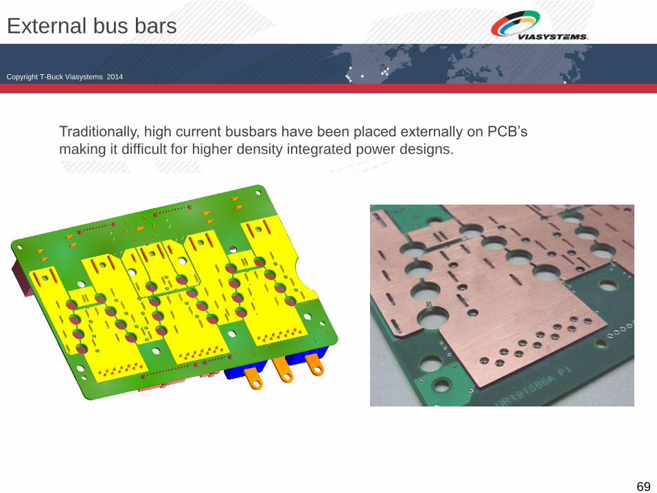
External bus bars
69
Traditionally, high current busbars have been placed externally on PCB’s
making it difficult for higher density integrated power designs.

Use or disclosure of information contained on this page is subject to the restriction on page 2 of this document
∂
Copyright T-Buck Viasystems 2014
Embedded Busbar Technology
• Increasing current as well as
thermal dissipation are
driving the need for copper
thicker
• When copper thickness
exceeds practical etching
technologies embedded bus-
bars become practical
• Embedded busbars take
advantage of the fact that
they can pre-machined with
precision prior to board
fabrication
• Once the board is fabricated
the bus-bar becomes an
integral part of the finished
PCB

Use or disclosure of information contained on this page is subject to the restriction on page 2 of this document
∂
Copyright T-Buck Viasystems 2014
Embedded Busbar Technology
Copper stock Precision machining
Pre-machined Busbar Finished PCB

Use or disclosure of information contained on this page is subject to the restriction on page 2 of this document
∂
Copyright T-Buck Viasystems 2014
Embedded Busbar PCB Manufacturing
Use a 5L stack-up (a few layers without copper). 2 cores & 2 layers of
copper foil are used, use prepreg to fix the Busbar and ensure no resin
void around the Busbar. (refer to the stack-up bellow).
14mil Core
14mil Core
7628 prepreg
Copper foil
Copper foil Core
Prepreg
Copper foil
Prepregs
Core
Layer 1
Layer 2
Layer 3
Layer 4
Layer 5
No Pattern
No Pattern

Use or disclosure of information contained on this page is subject to the restriction on page 2 of this document
∂
Copyright T-Buck Viasystems 2014
73
PCB Design; L1 Solder Mask and Cavities.
L1 Pattern (red)
Soldermask clearances (yellow)
4 cavities to be created by depth
controlled routing to expose
busbar (blue)
Cavities will (during assembling)
be filled with solder and soldered
to Mosfet body for conducting
electrical current and heat.
3 busbar leads which extend the PCB must be
reduced in thickness by controlled depth routing

Use or disclosure of information contained on this page is subject to the restriction on page 2 of this document
∂
Copyright T-Buck Viasystems 2014
Lamination process
74
Pre routed
core
Copper
Busbar
prepreg Composite substrate with
embedded busbars

Use or disclosure of information contained on this page is subject to the restriction on page 2 of this document
∂
Copyright T-Buck Viasystems 2014
Busbar Cross-Section
• There is no gap and void between busbar and laminate.
• Resin completely filled the gap.
75
Embedded
Copper
Busbar

Use or disclosure of information contained on this page is subject to the restriction on page 2 of this document
∂
Copyright T-Buck Viasystems 2014
76
Finished Circuit
Top side view Bottom side view
Use or disclosure of information contained on this page is subject to the restriction on page 2 of this document
∂
Copyright T-Buck Viasystems 2014
Overview
C²eT
Controlled Copper Etch Technology
Precision Features For RF and
Microwave Applications

Use or disclosure of information contained on this page is subject to the restriction on page 2 of this document
∂
Copyright T-Buck Viasystems 2014
• RF and microwave circuits generally require printed components such as
antenna, filters, couplers, resonators and precision taps
• As frequencies increase printed component size decreases with a demand for
improved conductor resolution i.e. precise trace and space
• Current designs are demanding finished trace and space tolerance to be +/-
0.0005” to 0.0007” (predicated on customers demand for performance)
• Pattern plating on surface layers reduced conductor resolution
• Via-In-Pad required in many designs introduces wrap plating, increasing the
background copper that must be etched, further reducing resolution
• Producing Foil Only etched features eliminates the plating and wrap plating in
feature regions improving resolution
Why Use Foil Only Features ?
78

Use or disclosure of information contained on this page is subject to the restriction on page 2 of this document
∂
Copyright T-Buck Viasystems 2014
Filter image etched into
Outer layer foil, no plating
Pattern platting process
for via plating and non-
critical circuit formation
Applications In RF & Microwave Circuits
79

Use or disclosure of information contained on this page is subject to the restriction on page 2 of this document
∂
Copyright T-Buck Viasystems 2014
80
Rogers 6002 0.010” 1/2 oz + Plt
1/2 oz
Layer 1
Layer 2
Laminate Core RF Signal Layer
370 HR 2X 10⁶ Prepreg
Layer 3
Layer 4
370HR 0.008” 1/2 oz
1/2 oz + Plt Laminate Core
Mixed Signal Layer
Mixed Signal Layer
Mechanical drill
standard pattern
plating
Laser drill standard
pattern plating
Foil
only
region
Sample stack-up of RF & Microwave job

Use or disclosure of information contained on this page is subject to the restriction on page 2 of this document
∂
Copyright T-Buck Viasystems 2014
Example of PCB Outer Layer
81
RF Outer Layer With Printed Filters
Pattern plated
region
Foil only
region
• Foil region consists of only foil and Cu flash plate
• Pattern plate region, standard copper thickness
• Photo tools are required for:
Foil only print and etch
Pattern plate tools with foil only isolation
Foil only photo tool to protect Foil Only region
in final etch

Use or disclosure of information contained on this page is subject to the restriction on page 2 of this document
∂
Copyright T-Buck Viasystems 2014
Filter Print & Etch For Foil Only Region
82
Foil Only regions defining printed RF components
The defined regions will be Foil Only for precise etching.
Copper consists of only foil and Cu flash plate in the case
of Teflon outer layer dielectric materials such as the Rogers
6002 used in this example

Use or disclosure of information contained on this page is subject to the restriction on page 2 of this document
∂
Copyright T-Buck Viasystems 2014
Pattern Plate Artwork
Foil Only regions are masked with LDI
photo resist during the pattern plate
process
83
Critical interface between the Foil Only
region and the raised copper pattern
plate surface
Illustration of Foil Only and pattern plate
definition
Pattern plate image

Use or disclosure of information contained on this page is subject to the restriction on page 2 of this document
∂
Copyright T-Buck Viasystems 2014
Foil Only Features On Surface Plated Layers
Standard copper
pattern plate
Foil only region
Trace cross-section A-A
A A
Plated region Transition region Foil region
Transition region
84

Use or disclosure of information contained on this page is subject to the restriction on page 2 of this document
∂
Copyright T-Buck Viasystems 2014
Board # A-1 (line) A-2(space) A-3(line) B-1(line) B-2(space) B-3(line) C-1(line) C-2(space) C-3(line) D-1(line) D-2(space) D-3(line)
Nominal 9.00 13.00 9.00 9.00 13.00 9.00 7.00 5.00 7.00 7.00 5.00 7.00
1 8.43 13.49 8.57 8.5 13.42 8.44 6.6 5.41 6.53 6.61 5.27 6.45
2 8.5 13.42 8.56 8.71 13.43 8.64 6.74 5.27 6.61 6.75 5.34 6.47
3 8.64 13.35 8.71 8.64 13.42 8.57 6.84 5.2 6.85 6.68 5.41 6.68
4 8.57 13.49 8.5 8.57 13.28 8.57 6.53 5.34 6.61 6.61 5.48 6.53
5 8.57 13.35 8.71 8.64 13.21 8.71 6.54 5.27 6.67 6.47 5.48 6.47
6 8.71 13.28 8.64 8.64 13.21 8.73 6.81 5.13 6.82 6.6 5.27 6.68
7 8.57 13.42 8.64 8.57 13.35 8.64 6.6 5.27 6.6 6.61 5.41 6.53
8 8.5 13.42 8.5 8.5 13.56 8.57 6.46 5.55 6.53 6.46 5.41 6.47
9 8.78 13.28 8.65 8.65 13.42 8.64 6.96 5.06 6.89 6.61 5.27 6.67
10 8.71 13.29 8.62 8.5 13.45 8.57 6.48 5.55 6.6 6.54 5.41 6.53
Average 8.598 13.379 8.61 8.592 13.375 8.608 6.656 5.305 6.671 6.594 5.375 6.548
Diff from Avg. -0.40 0.38 -0.39 -0.41 0.38 -0.39 -0.34 0.31 -0.33 -0.41 0.37 -0.45
First Pass Line Width Tolerance: Foil Region
• Line widths were evaluated on non-
compensated etched traces
• Average values were obtained yielding a
tolerance based on the difference from the
average values. First pass results better than
+/- 0.0005”
85

Use or disclosure of information contained on this page is subject to the restriction on page 2 of this document
∂
Copyright T-Buck Viasystems 2014
86
Finished Hybrid PCB With Foil Only Features

Use or disclosure of information contained on this page is subject to the restriction on page 2 of this document
∂
Copyright T-Buck Viasystems 2014
Summary
…Sometimes a little more time spent on
a design can dramatically reduce cost
• Start designs by defining the technology limiting packages
• Look for a power delivery solution first
• Define the minimum technology set for the PCB design
• Review the design interactions with the technologies selected
• Make sure the technology level is compatible with your PCB supply chain
• Rethink design strategies before “bending” the rules
Today’s advanced electronic systems require a complex
blend of many process technologies that must work in
concert to provide interconnect solutions. Good
engineering and careful planning lead to quality results…

Use or disclosure of information contained on this page is subject to the restriction on page 2 of this document
∂
Copyright T-Buck Viasystems 2014
Workshop Objectives
Thank You !