the future of micro-contamination control in … future of micro-contamination control in chemical...
TRANSCRIPT
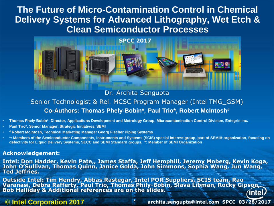
The Future of Micro-Contamination Control in Chemical Delivery Systems for Advanced Lithography, Wet Etch &
Clean Semiconductor Processes
Dr. Archita Sengupta
Senior Technologist & Rel. MCSC Program Manager (Intel TMG_GSM)
Co-Authors: Thomas Phely-Bobin*, Paul Trio*, Robert McIntosh#
• Thomas Phely-Bobin*, Director, Applications Development and Metrology Group, Microcontamination Control Division, Entegris Inc.
• Paul Trio*, Senior Manager, Strategic Initiatives, SEMI
• # Robert McIntosh, Technical Marketing Manager Georg Fischer Piping Systems
• *: Members of the Semiconductor Components, Instruments and Systems (SCIS) special interest group, part of SEMI® organization, focusing on defectivity for Liquid Delivery Systems, SECC and SEMI Standard groups. *: Member of SEMI Organization
Acknowledgement:
Intel: Don Hadder, Kevin Pate,, James Staffa, Jeff Hemphill, Jeremy Moberg, Kevin Koga, John O’Sullivan, Thomas Quinn, Janice Golda, John Simmons, Sophia Wang, Jun Wang, Ted Jeffries.
Outside Intel: Tim Hendry, Abbas Rastegar, Intel POR Suppliers, SCIS team, RaoVaranasi, Debra Rafferty, Paul Trio, Thomas Phily-Bobin, Slava Libman, Rocky Gipson, Bob Halliday & Additional references are on the slides.
• [email protected] SPCC 03/28/2017© Intel Corporation 2017
SPCC 2017
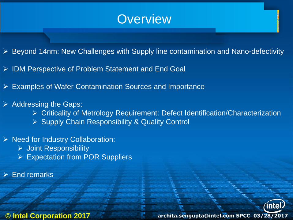
Overview
[email protected] SPCC 03/28/2017
Beyond 14nm: New Challenges with Supply line contamination and Nano-defectivity
IDM Perspective of Problem Statement and End Goal
Examples of Wafer Contamination Sources and Importance
Addressing the Gaps:
Criticality of Metrology Requirement: Defect Identification/Characterization
Supply Chain Responsibility & Quality Control
Need for Industry Collaboration:
Joint Responsibility
Expectation from POR Suppliers
End remarks
© Intel Corporation 2017
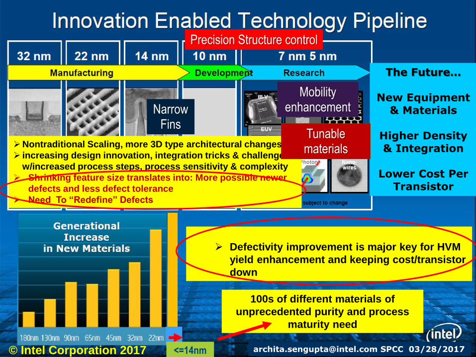
Innovation Enabled Technology Pipeline
3
Future options subject to change
32 nm 22 nm 14 nm 10 nm 7 nm 5 nm
GrapheneIII-V 3-D
Materials
Synthesis
Dense Memory
EUV
Interconnects
Nano-wires
Photonics
Manufacturing Development Research The Future…
New Equipment & Materials
Higher Density & Integration
Lower Cost Per Transistor
[email protected] GSM 09/21/2016
Generational Increase
in New Materials
Lithography Scaling and Cost of Ownership Enable
Moore’s Law
Shrinking feature size is adding more possible
defects/challenges and less defect tolerance
Defectivity improvement is major key for HMV yield
improvement and keeping cost/transistor down
increasing design
innovation, process
sensitivity & complexity
The Future…
New Equipment & Materials
Higher Density & Integration
Lower Cost Per Transistor
Defectivity improvement is major key for HVM
yield enhancement and keeping cost/transistor
down
Nontraditional Scaling, more 3D type architectural changes
increasing design innovation, integration tricks & challenges
w/increased process steps, process sensitivity & complexity
Shrinking feature size translates into: More possible newer
defects and less defect tolerance
Need To “Redefine” Defects
100s of different materials of
unprecedented purity and process
maturity need
<=14nm© Intel Corporation 2017 [email protected] SPCC 03/28/2017
Narrow Fins
Tunable materials
Mobility enhancement
Precision Structure control
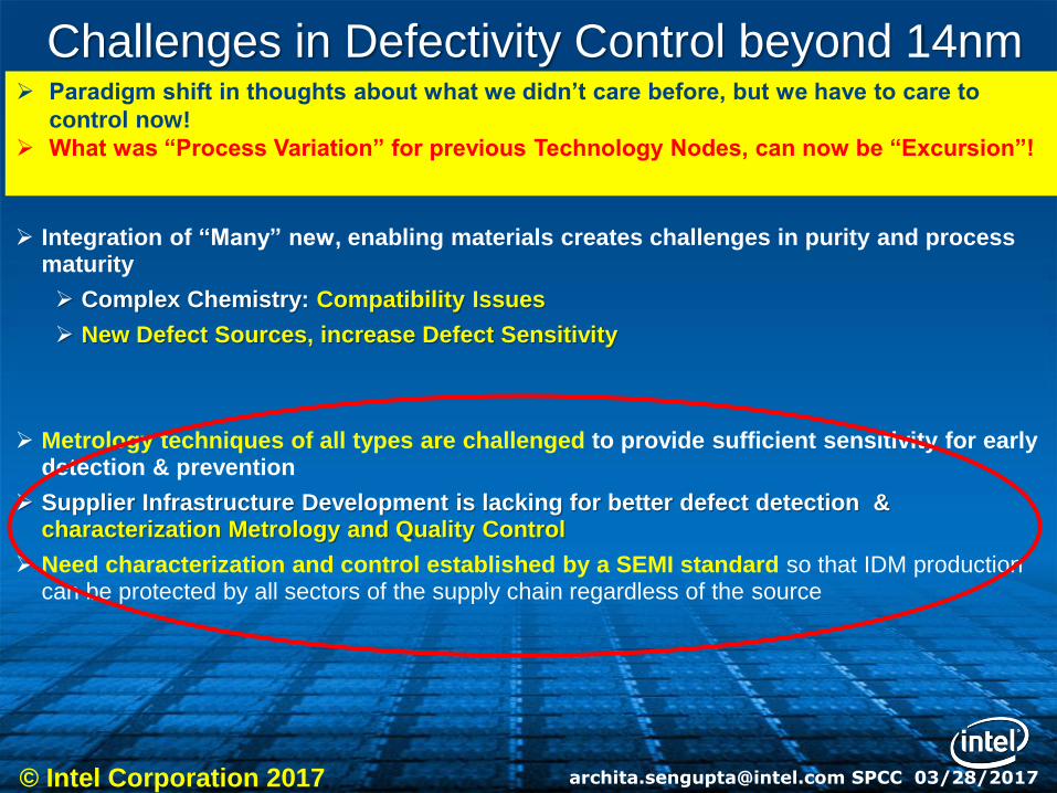
Integration of “Many” new, enabling materials creates challenges in purity and process maturity
Complex Chemistry: Compatibility Issues
New Defect Sources, increase Defect Sensitivity
Metrology techniques of all types are challenged to provide sufficient sensitivity for early detection & prevention
Supplier Infrastructure Development is lacking for better defect detection & characterization Metrology and Quality Control
Need characterization and control established by a SEMI standard so that IDM production can be protected by all sectors of the supply chain regardless of the source
[email protected] SPCC 03/28/2017
Challenges in Defectivity Control beyond 14nm
© Intel Corporation 2017
Paradigm shift in thoughts about what we didn’t care before, but we have to care to
control now!
What was “Process Variation” for previous Technology Nodes, can now be “Excursion”!
HVM Requirements
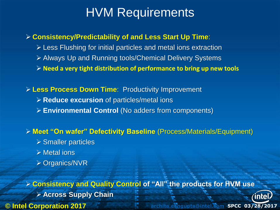
Consistency/Predictability of and Less Start Up Time:
Less Flushing for initial particles and metal ions extraction
Always Up and Running tools/Chemical Delivery Systems
Need a very tight distribution of performance to bring up new tools
Less Process Down Time: Productivity Improvement
Reduce excursion of particles/metal ions
Environmental Control (No adders from components)
Meet “On wafer” Defectivity Baseline (Process/Materials/Equipment)
Smaller particles
Metal ions
Organics/NVR
Consistency and Quality Control of “All” the products for HVM use
Across Supply Chain
[email protected] SPCC 03/28/2017© Intel Corporation 2017
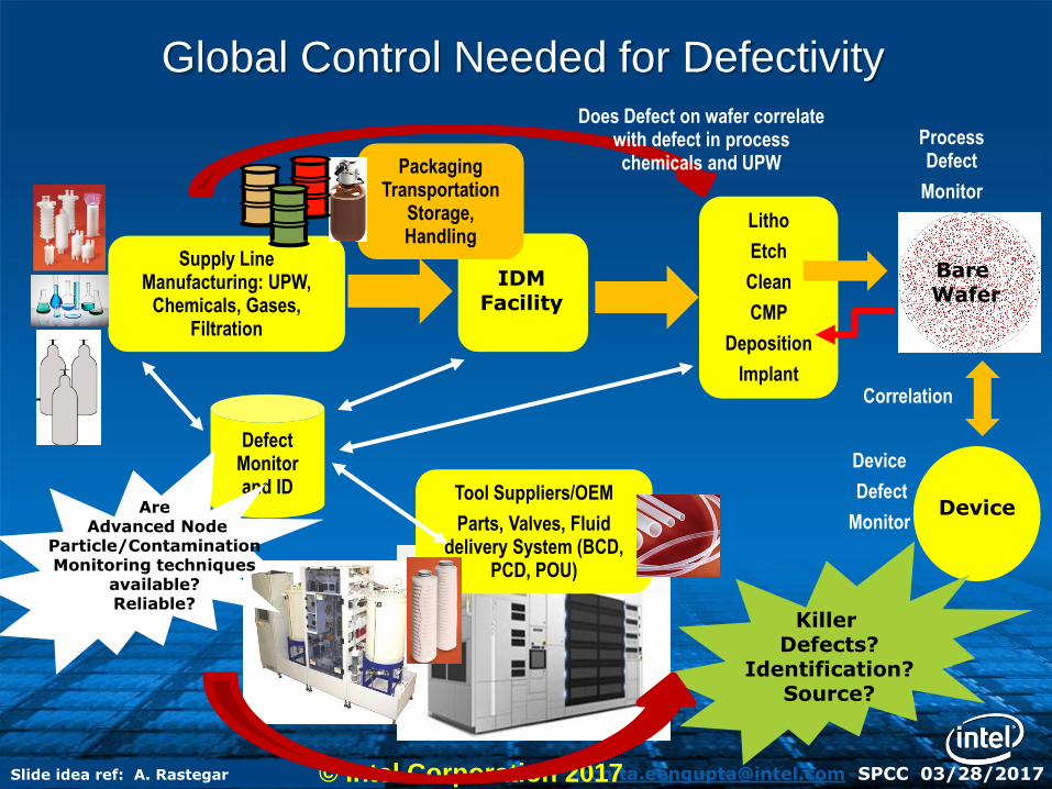
Global Control Needed for Defectivity
Supply Line Manufacturing: UPW,
Chemicals, Gases, Filtration
Defect Monitor and ID
Litho
Etch
Clean
CMP
Deposition
Implant
Device
Killer Defects?
Identification?Source?
IDMFacility
Correlation
Packaging Transportation
Storage, Handling
Process Defect
Monitor
Device
Defect
Monitor
BareWafer
AreAdvanced Node
Particle/Contamination Monitoring techniques
available?Reliable?
Slide idea ref: A. Rastegar
Does Defect on wafer correlate with defect in process chemicals and UPW
Tool Suppliers/OEM
Parts, Valves, Fluid delivery System (BCD,
PCD, POU)
[email protected] SPCC 03/28/2017© Intel Corporation 2017
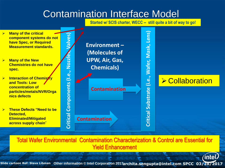
Contamination Interface Model
Environment –(Molecules ofUPW, Air, Gas,
Chemicals)
Contamination
Contamination
Cri
tica
l Su
bst
rate
(i.
e.,
Waf
er,
Mas
k, L
en
s)
Cri
tica
l Co
mp
on
ents
(I.
e.,
No
zzle
s, V
alve
s)
Secondary Critical Systems/Environments (i.e., PCW)
Slide cartoon Ref: Slava Libman
Many of the critical
component systems do not
have Spec, or Required
Measurement standards.
Many of the New
Chemistries do not have
spec.
Interaction of Chemistry
and Tools: Low
concentration of
particles/metals/NVR/Orga
nics defects
These Defects “Need to be
Detected,
Eliminated/Mitigated
across supply chain”
Collaboration
Other information © Intel Corporation [email protected] SPCC 03/28/2017
Started w/ SCIS charter, WECC -- still quite a bit of way to go!
Total Wafer Environmental Contamination Characterization & Control are Essential for Yield Enhancement
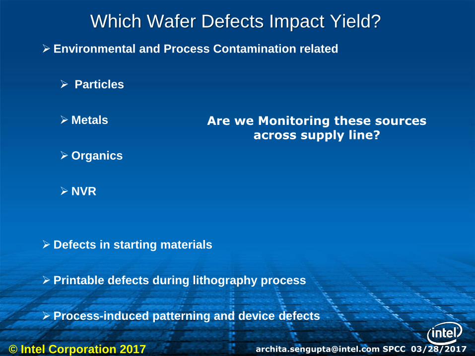
Which Wafer Defects Impact Yield?
Environmental and Process Contamination related
Particles
Metals
Organics
NVR
Defects in starting materials
Printable defects during lithography process
Process-induced patterning and device defects
Are we Monitoring these sources across supply line?
© Intel Corporation 2017 [email protected] SPCC 03/28/2017
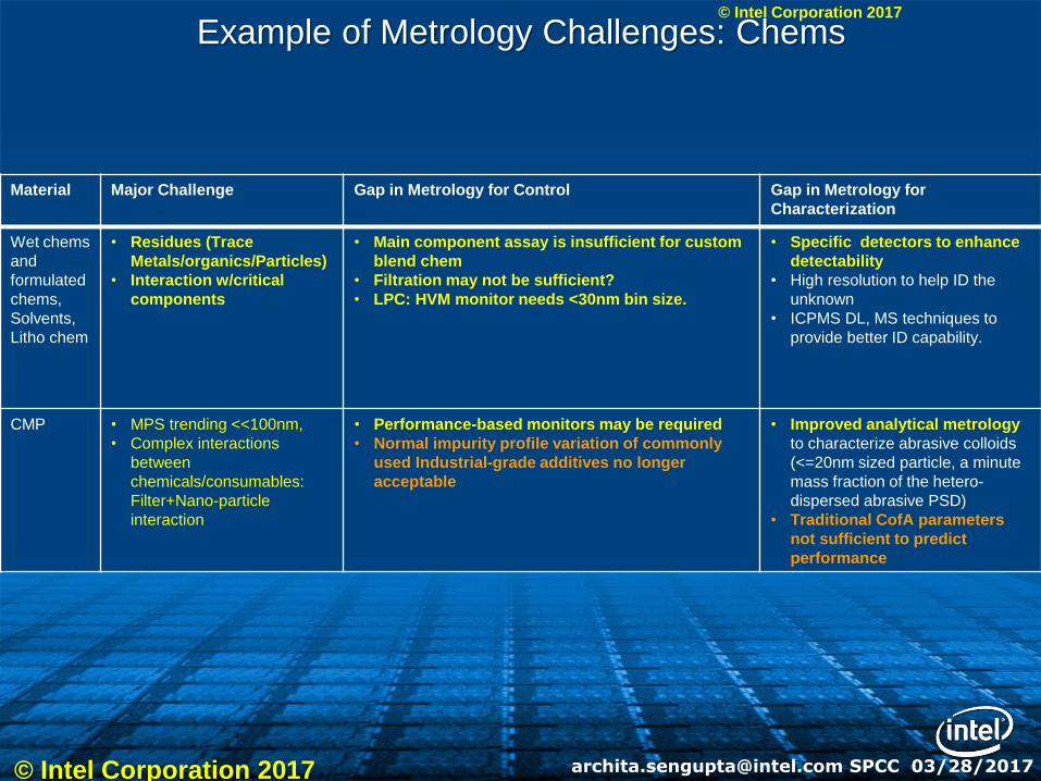
Material Major Challenge Gap in Metrology for Control Gap in Metrology for
Characterization
Wet chems
and
formulated
chems,
Solvents,
Litho chem
• Residues (Trace
Metals/organics/Particles)
• Interaction w/critical
components
• Main component assay is insufficient for custom
blend chem
• Filtration may not be sufficient?
• LPC: HVM monitor needs <30nm bin size.
• Specific detectors to enhance
detectability
• High resolution to help ID the
unknown
• ICPMS DL, MS techniques to
provide better ID capability.
CMP • MPS trending <<100nm,
• Complex interactions
between
chemicals/consumables:
Filter+Nano-particle
interaction
• Performance-based monitors may be required
• Normal impurity profile variation of commonly
used Industrial-grade additives no longer
acceptable
• Improved analytical metrology
to characterize abrasive colloids
(<=20nm sized particle, a minute
mass fraction of the hetero-
dispersed abrasive PSD)
• Traditional CofA parameters
not sufficient to predict
performance
Example of Metrology Challenges: Chems© Intel Corporation 2017
© Intel Corporation 2017 [email protected] SPCC 03/28/2017
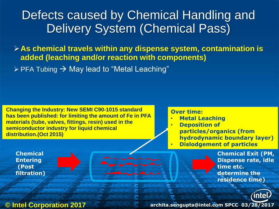
Defects caused by Chemical Handling and Delivery System (Chemical Pass)
As chemical travels within any dispense system, contamination is added (leaching and/or reaction with components)
PFA Tubing May lead to “Metal Leaching”
Chemical Entering(Post filtration)
Chemical Exit (PM, Dispense rate, idle time etc. determine the residence time)
[email protected] SPCC 03/28/2017
Over time: • Metal Leaching• Deposition of
particles/organics (from hydrodynamic boundary layer)
• Dislodgement of particles
© Intel Corporation 2017
Changing the Industry: New SEMI C90-1015 standard has been published: for limiting the amount of Fe in PFA materials (tube, valves, fittings, resin) used in the semiconductor industry for liquid chemical distribution.(Oct 2015)
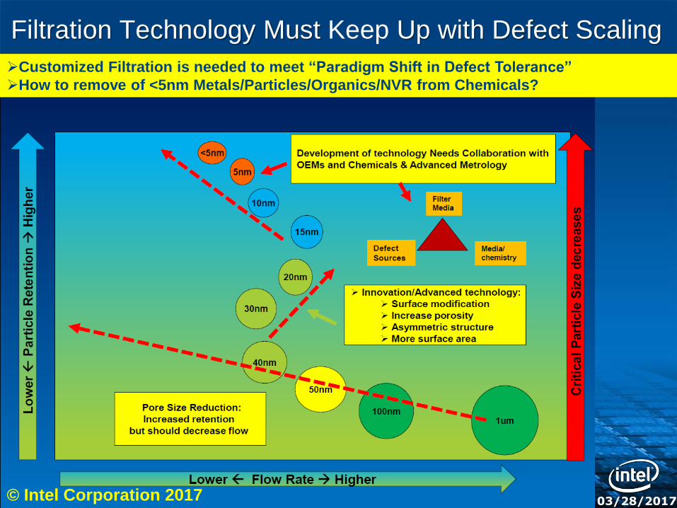
Filtration Technology Must Keep Up with Defect Scaling
Customized Filtration is needed to meet “Paradigm Shift in Defect Tolerance”
How to remove of <5nm Metals/Particles/Organics/NVR from Chemicals?
03/28/2017© Intel Corporation 2017
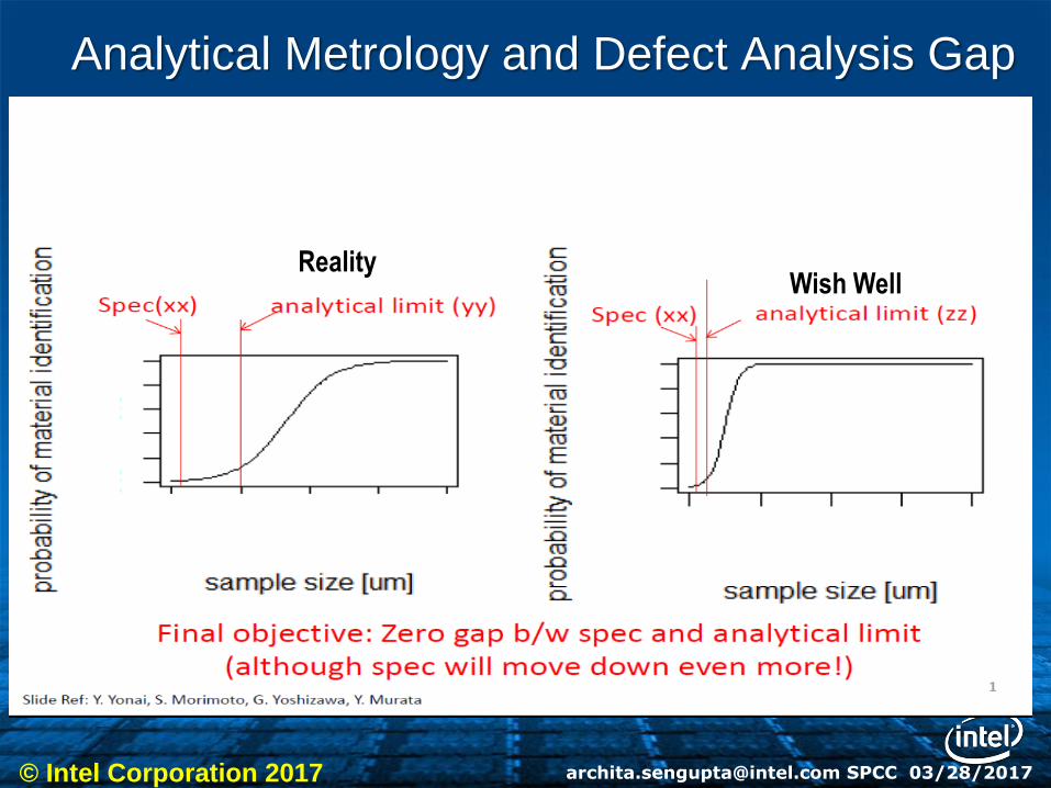
Analytical Metrology and Defect Analysis Gap
Wish WellReality
[email protected] SPCC 03/28/2017© Intel Corporation 2017
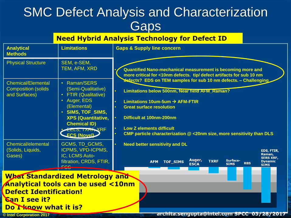
SMC Defect Analysis and Characterization Gaps
Analytical
Methods
Limitations Gaps & Supply line concern
Physical Structure SEM, e-SEM,
TEM, AFM, XRD
Chemical/Elemental
Composition (solids
and Surfaces)
• Raman/SERS
(Semi-Qualitative)
• FTIR (Qualitative)
• Auger, EDS
(Elemental)
• SIMS, TOF_SIMS,
XPS (Quantitative,
Chemical ID)
• EELS, TXRF, XRF
• FCS (Novel)
Chemical/elemental
(Solids, Liquids,
Gases)
GCMS, TD_GCMS,
ICPMS, VPD-ICPMS,
IC, LCMS Auto-
filtration, CRDS, FTIR,
FCS
• Quantified Nano-mechanical measurement is becoming more and
more critical for <10nm defects. tip/ defect artifacts for sub 10 nm
defects? EDS on TEM samples for sub 10 nm defects. – Challenging
• Limitations below 500nm, Near field AFM_Raman?
• Limitations 10um-5um AFM-FTIR
• Great surface resolution
• Difficult at 100nm-200nm
• Low Z elements difficult
• CMP particle characterization @ <20nm size, more sensitivity than DLS
• Need better sensitivity and DL
Need Hybrid Analysis Technology for Defect ID
© Intel Corporation 2017
What Standardized Metrology and Analytical tools can be used <10nm Defect Identification! Can I see it?Do I know what it is?
[email protected] SPCC 03/28/2017
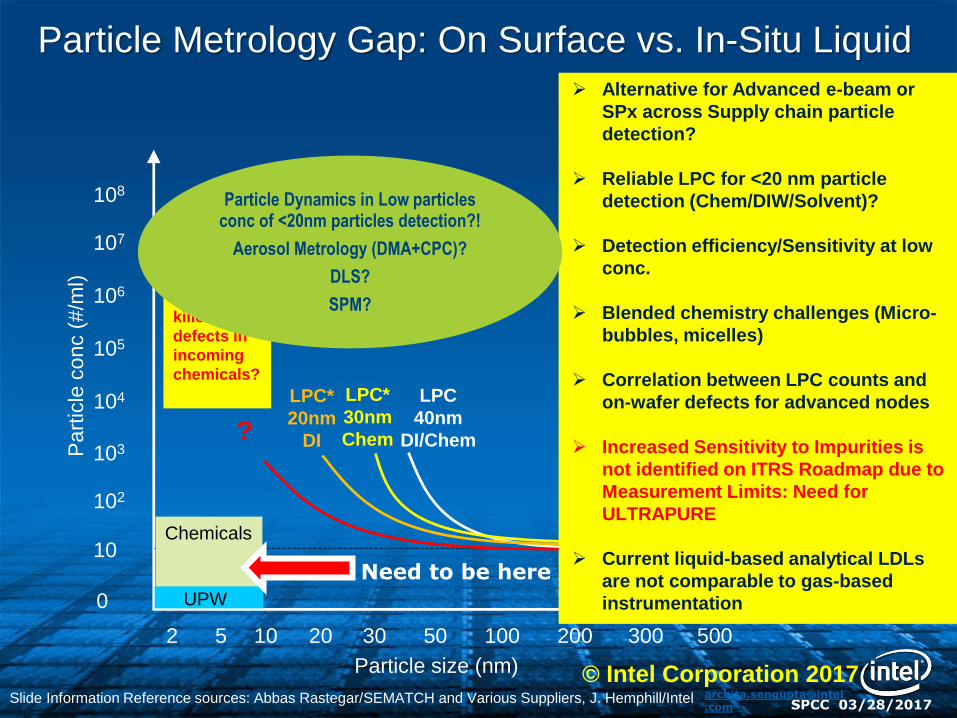
Particle Metrology Gap: On Surface vs. In-Situ Liquid
0
10
102
103
104
105
106
107
108
2 5 10 20 30 50 100 200 300 500
Particle size (nm)
Part
icle
conc (
#/m
l)
LPC
40nm
DI/Chem
LPC*
30nm
Chem
LPC*
20nm
DI
UPW
Chemicals
Slide Information Reference sources: Abbas Rastegar/SEMATCH and Various Suppliers, J. Hemphill/Intel
Need to be here
?
SPCC 03/28/2017
“Blind” to
killer
defects in
incoming
chemicals?
© Intel Corporation 2017
Alternative for Advanced e-beam or
SPx across Supply chain particle
detection?
Reliable LPC for <20 nm particle
detection (Chem/DIW/Solvent)?
Detection efficiency/Sensitivity at low
conc.
Blended chemistry challenges (Micro-
bubbles, micelles)
Correlation between LPC counts and
on-wafer defects for advanced nodes
Increased Sensitivity to Impurities is
not identified on ITRS Roadmap due to
Measurement Limits: Need for
ULTRAPURE
Current liquid-based analytical LDLs
are not comparable to gas-based
instrumentation
Particle Dynamics in Low particles conc of <20nm particles detection?!
Aerosol Metrology (DMA+CPC)?
DLS?
SPM?
How do we Control/Prevent the Contaminants?
1st Request: Three major control of the contaminants before ship the “Best” products to the factory:
The Materials
The Equipment
The Components
2nd Request: We Cannot Evaluate Advanced Node Chemistry/Process Without Aggressive “Super-Filtration And Purification”
Need ultrapure materials, extreme retention, lowest possible interaction
Optimized at chemical manufacturing and at factory processing/tools
3rd Request: Help us closing the Metrology/Analysis/Standard Gaps
4th Request: Work Together: Collaboration
[email protected] SPCC 03/28/2017
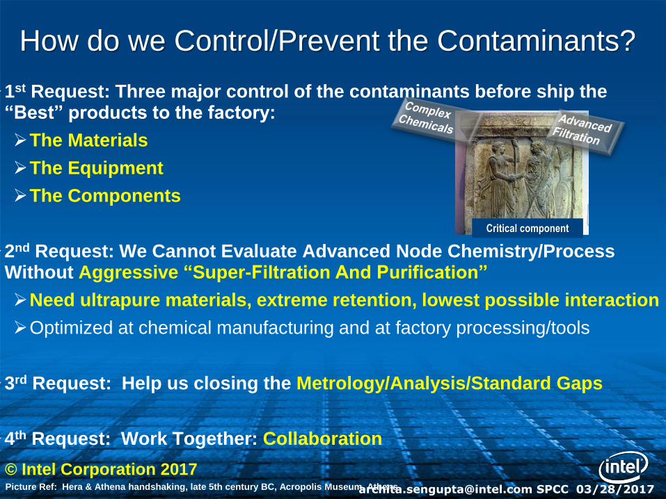
Critical component
Picture Ref: Hera & Athena handshaking, late 5th century BC, Acropolis Museum, Athens
© Intel Corporation 2017
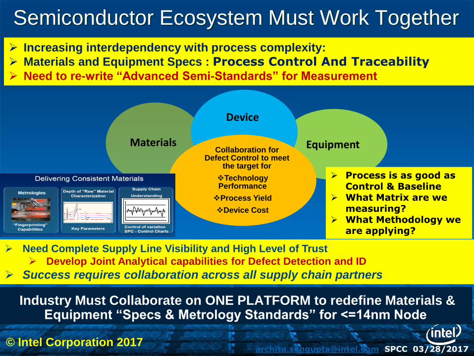
Semiconductor Ecosystem Must Work Together
EquipmentMaterials
Increasing interdependency with process complexity:
Materials and Equipment Specs : Process Control And Traceability Need to re-write “Advanced Semi-Standards” for Measurement
Need Complete Supply Line Visibility and High Level of Trust
Develop Joint Analytical capabilities for Defect Detection and ID
Success requires collaboration across all supply chain partners
Collaboration for Defect Control to meet
the target for
Technology Performance
Process Yield
Device Cost
Device
[email protected] SPCC 03/28/2017
Industry Must Collaborate on ONE PLATFORM to redefine Materials & Equipment “Specs & Metrology Standards” for <=14nm Node
© Intel Corporation 2017
Process is as good as Control & Baseline
What Matrix are we measuring?
What Methodology we are applying?
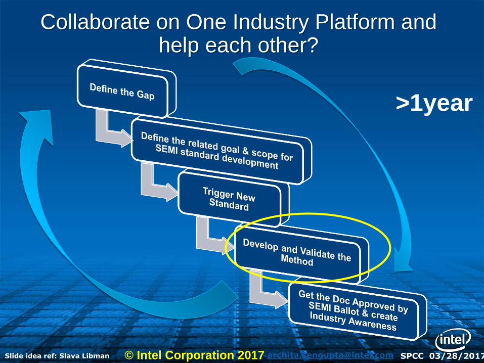
Collaborate on One Industry Platform and help each other?
>1year
Slide idea ref: Slava Libman © Intel Corporation 2017 [email protected] SPCC 03/28/2017
SPCC 03/28/2017
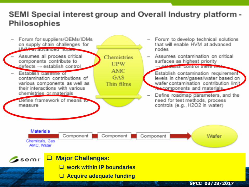
Major Challenges:
work within IP boundaries
Acquire adequate funding
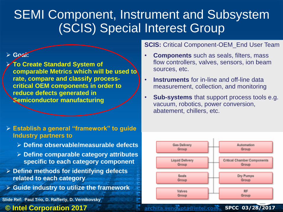
Goal:
To Create Standard System of comparable Metrics which will be used to rate, compare and classify process-critical OEM components in order to reduce defects generated in Semiconductor manufacturing
Establish a general “framework” to guide Industry partners to
Define observable/measurable defects
Define comparable category attributes specific to each category component
Define methods for identifying defects related to each category
Guide industry to utilize the framework
SEMI Component, Instrument and Subsystem (SCIS) Special Interest Group
SCIS: Critical Component-OEM_End User Team
• Components such as seals, filters, mass flow controllers, valves, sensors, ion beam sources, etc.
• Instruments for in-line and off-line data measurement, collection, and monitoring
• Sub-systems that support process tools e.g. vacuum, robotics, power conversion, abatement, chillers, etc.
Slide Ref: Paul Trio, D. Rafferty, D. Vernikovsky
© Intel Corporation 2017 [email protected] SPCC 03/28/2017
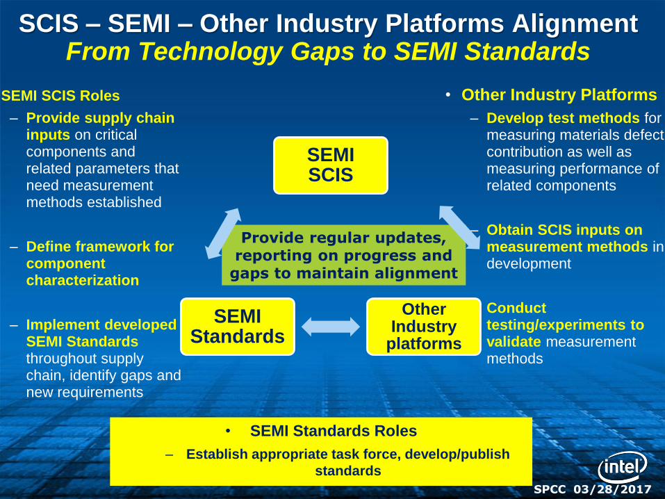
SCIS – SEMI – Other Industry Platforms AlignmentFrom Technology Gaps to SEMI Standards
SEMI SCIS Roles
– Provide supply chain inputs on critical components and related parameters that need measurement methods established
– Define framework for component characterization
– Implement developed SEMI Standards throughout supply chain, identify gaps and new requirements
• Other Industry Platforms
– Develop test methods for measuring materials defect contribution as well as measuring performance of related components
– Obtain SCIS inputs on measurement methods in development
– Conduct testing/experiments to validate measurement methods
• SEMI Standards Roles
– Establish appropriate task force, develop/publish
standards
Provide regular updates, reporting on progress and
gaps to maintain alignment
SEMI SCIS
Other Industry
platforms
SEMI Standards
SPCC 03/28/2017
SPCC 03/28/2017
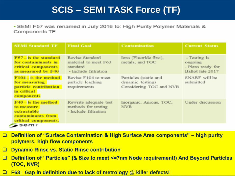
Definition of “Surface Contamination & High Surface Area components” – high purity
polymers, high flow components
Dynamic Rinse vs. Static Rinse contribution
Definition of “Particles” (& Size to meet <=7nm Node requirement!) And Beyond Particles
(TOC, NVR)
F63: Gap in definition due to lack of metrology @ killer defects!
SCIS – SEMI TASK Force (TF)
SPCC 03/28/2017
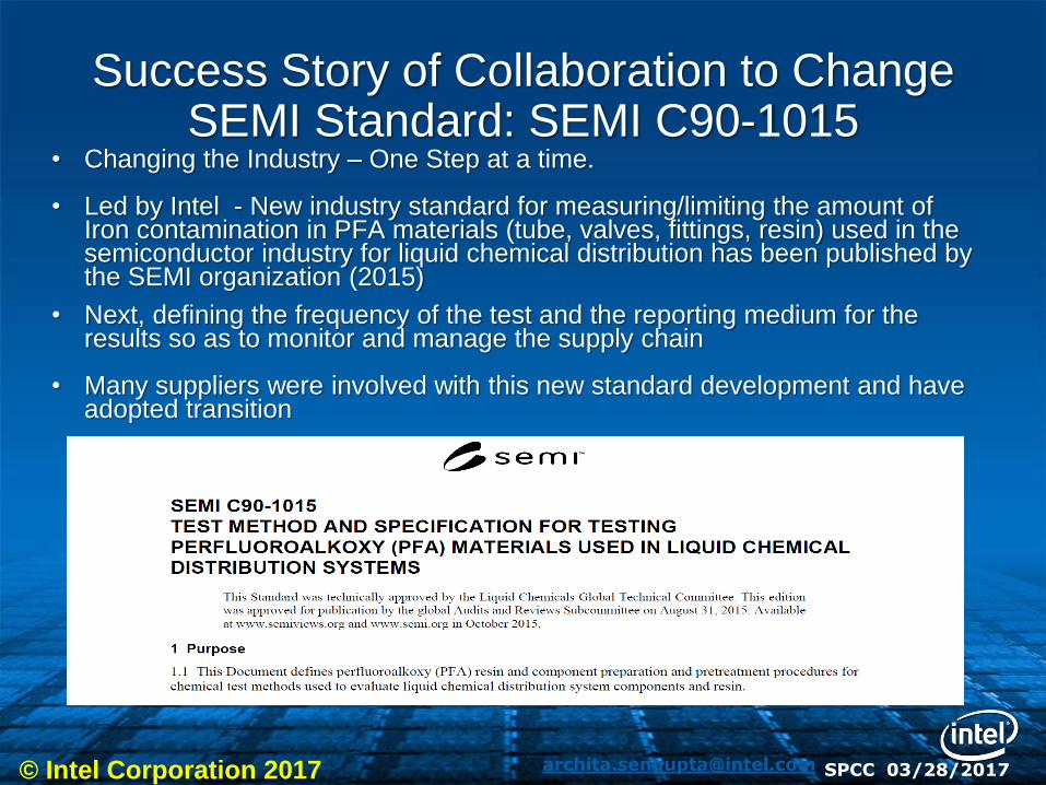
Success Story of Collaboration to Change SEMI Standard: SEMI C90-1015
• Changing the Industry – One Step at a time.
• Led by Intel - New industry standard for measuring/limiting the amount of Iron contamination in PFA materials (tube, valves, fittings, resin) used in the semiconductor industry for liquid chemical distribution has been published by the SEMI organization (2015)
• Next, defining the frequency of the test and the reporting medium for the results so as to monitor and manage the supply chain
• Many suppliers were involved with this new standard development and have adopted transition
© Intel Corporation 2017 [email protected] SPCC 03/28/2017
Leadership means Corporate Responsibility
14nm and Beyond: We have paradigm shift in process scaling/defectivity challenges: Process Variation can end up as Excursion
Interdisciplinary expertise need to work together
– Tool suppliers, Material suppliers, Filter Suppliers, Component suppliers, Metrology suppliers and IDMs need to work together to achieve required defectivity baseline and create new STANDARDS
• Next Generation Quality Systems combined with Sub-Supplier Management helps to achieve “Ship to Control Across Supply Chain”, makes IDM “Quality Incident Free” and minimize costly learning during HVM ramp
End Reflection
© Intel Corporation 2017 [email protected] SPCC 03/28/2017
Archita
SPCC 03/28/2017© Intel Corporation 2017
Thank YOU
• To My Co-Authors• All My Intel colleagues for contributing to the content of the presentation• To Abbas Rastegar as referenced and always providing valuable input
• To All Intel Suppliers: Thank You for Your Valued Partnership • To SPCC Committee for the opportunity to present
Risk Factors
• The above statements and any others in this document that refer to plans and expectations for the first quarter, the year and the future are forward-looking statements that involve a number of risks and uncertainties. Words such as “anticipates,” “expects,” “intends,” “plans,” “believes,” “seeks,” “estimates,” “may,” “will,” “should” and their variations identify forward-looking statements. Statements that refer to or are based on projections, uncertain events or assumptions also identify forward-looking statements. Many factors could affect Intel’s actual results, and variances from Intel’s current expectations regarding such factors could cause actual results to differ materially from those expressed in these forward-looking statements. Intel presently considers the following to be the important factors that could cause actual results to differ materially from the company’s expectations. Demand could be different from Intel's expectations due to factors including changes in business and economic conditions, including supply constraints and other disruptions affecting customers; customer acceptance of Intel’s and competitors’ products; changes in customer order patterns including order cancellations; and changes in the level of inventory at customers. Uncertainty in global economic and financial conditions poses a risk that consumers and businesses may defer purchases in response to negative financial events, which could negatively affect product demand and other related matters. Intel operates in intensely competitive industries that are characterized by a high percentage of costs that are fixed or difficult to reduce in the short term and product demand that is highly variable and difficult to forecast. Revenue and the gross margin percentage are affected by the timing of Intel product introductions and the demand for and market acceptance of Intel's products; actions taken by Intel's competitors, including product offerings and introductions, marketing programs and pricing pressures and Intel’s response to such actions; and Intel’s ability to respond quickly to technological developments and to incorporate new features into its products. Intel is in the process of transitioning to its next generation of products on 22nm process technology, and there could be execution and timing issues associated with these changes, including products defects and errata and lower than anticipated manufacturing yields. The gross margin percentage could vary significantly from expectations based on capacity utilization; variations in inventory valuation, including variations related to the timing of qualifying products for sale; changes in revenue levels; product mix and pricing; the timing and execution of the manufacturing ramp and associated costs; start-up costs; excess or obsolete inventory; changes in unit costs; defects or disruptions in the supply of materials or resources; product manufacturing quality/yields; and impairments of long-lived assets, including manufacturing, assembly/test and intangible assets. The majority of Intel’s non-marketable equity investment portfolio balance is concentrated in companies in the flash memory market segment, and declines in this market segment or changes in management’s plans with respect to Intel’s investments in this market segment could result in significant impairment charges, impacting restructuring charges as well as gains/losses on equity investments and interest and other. Intel's results could be affected by adverse economic, social, political and physical/infrastructure conditions in countries where Intel, its customers or its suppliers operate, including military conflict and other security risks, natural disasters, infrastructure disruptions, health concerns and fluctuations in currency exchange rates. Expenses, particularly certain marketing and compensation expenses, as well as restructuring and asset impairment charges, vary depending on the level of demand for Intel's products and the level of revenue and profits. Intel’s results could be affected by the timing of closing of acquisitions and divestitures. Intel's results could be affected by adverse effects associated with product defects and errata (deviations from published specifications), and by litigation or regulatory matters involving intellectual property, stockholder, consumer, antitrust and other issues, such as the litigation and regulatory matters described in Intel's SEC reports. An unfavorable ruling could include monetary damages or an injunction prohibiting us from manufacturing or selling one or more products, precluding particular business practices, impacting Intel’s ability to design its products, or requiring other remedies such as compulsory licensing of intellectual property. A detailed discussion of these and other factors that could affect Intel’s results is included in Intel’s SEC filings, including the annual report on Form 10-K for the fiscal year ended December 31, 2011.
Rev. 2/23/12