the herschel/pacs 2560 bolometers imaging camera
TRANSCRIPT
PROCEEDINGS OF SPIE
SPIEDigitalLibrary.org/conference-proceedings-of-spie
The Herschel/PACS 2560 bolometersimaging camera
Nicolas Billot, Patrick Agnèse, Jean-Louis Auguères,Alain Béguin, André Bouère, et al.
Nicolas Billot, Patrick Agnèse, Jean-Louis Auguères, Alain Béguin, AndréBouère, Olivier Boulade, Christophe Cara, Christelle Cloué, EricDoumayrou, Lionel Duband, Benoît Horeau, Isabelle Le Mer, JeanLepennec, Jérome Martignac, Koryo Okumura, Vincent Revéret, MarcSauvage, François Simoens, Laurent Vigroux, "The Herschel/PACS 2560bolometers imaging camera," Proc. SPIE 6265, Space Telescopes andInstrumentation I: Optical, Infrared, and Millimeter, 62650D (16 June 2006);doi: 10.1117/12.671154
Event: SPIE Astronomical Telescopes + Instrumentation, 2006, Orlando,Florida , United States
Downloaded From: https://www.spiedigitallibrary.org/conference-proceedings-of-spie on 9/11/2018 Terms of Use: https://www.spiedigitallibrary.org/terms-of-use
! # % % ( + - ( / 0 - 1 0 / ( /
Nicolas Billota, Patrick Agneseb, Jean-Louis Augueresa, Alain Beguinb, Andre Bouerea, Olivier
Bouladea, Christophe Caraa, Christelle Clouea, Eric Doumayroua, Lionel Dubandc, Benoıt
Horeaua, Isabelle Le Mera, Jean Le Penneca, Jerome Martignaca, Koryo Okumuraa, Vincent
Reveretd, Marc Sauvagea, Francois Simoensb and Laurent Vigrouxe
aService d’Astrophysique, DAPNIA, CEA Saclay, 91191 Gif sur Yvette, FRANCE;bLaboratoire Infra-Rouge, LETI, CEA Grenoble, 38054 Grenoble, FRANCE;
cService des Basses Temperatures, DRFMC, CEA Grenoble, 38054 Grenoble, FRANCE;dEuropean Southern Observatory, Vitacura, Casilla 19001 Santiago 19, CHILE;
eInstitut d’Astrophysique de Paris, 75014 Paris, FRANCE
ABSTRACT
The development program of the flight model imaging camera for the PACS instrument on-board the Herschelspacecraft is nearing completion. This camera has two channels covering the 60 to 210 microns wavelengthrange. The focal plane of the short wavelength channel is made of a mosaic of 2x4 3-sides buttable bolometerarrays (16x16 pixels each) for a total of 2048 pixels, while the long wavelength channel has a mosaic of 2 of thesame bolometer arrays for a total of 512 pixels. The 10 arrays have been fabricated, individually tested andintegrated in the photometer. They represent the first filled arrays of fully collectively built bolometers witha cold multiplexed readout, allowing for a properly sampled coverage of the full instrument field of view. Thecamera has been fully characterized and the ground calibration campaign will take place after its delivery tothe PACS consortium in mid 2006. The bolometers, working at a temperature of 300 mK, have a NEP closeto the BLIP limit and an optical bandwidth of 4 to 5 Hz that will permit the mapping of large sky areas.This paper briefly presents the concept and technology of the detectors as well as the cryocooler and the warmelectronics. Then we focus on the performances of the integrated focal planes (responsivity, NEP, low frequencynoise, bandwidth).
Keywords: bolometers, cryocooler, far infrared, imaging camera, multiplexing, filled bolometer arrays
1. INTRODUCTION
The Herschel Space Observatory is the third “corner stone” mission of the European Space Agency. It willbe launched by an Ariane 5 rocket in the course of 2008. Herschel will be equipped with the largest telescopeever sent in space (Ø 3.5m) and will carry out spectroscopic and imaging observations in the 60 µm to 670 µmwavelength range. Herschel’s payload consists of three instruments. (1) HIFI is a very high resolution heterodynespectrometer (R ∼ 107), (2) SPIRE is an imager and an imaging spectrometer, operating in the 210-670 µmband, using spider-web bolometers coupled to Winston cones (see ref. 1 for details), and (3) PACS covers the60-210 µm range and is both an imaging spectrometer using photo-conducting detectors, and an imager usingnovel technology bolometers described in this paper.
The main science objectives of Herschel are twofold. First, Herschel will perform large scale surveys of nearbydark clouds, regions where stars form, in order to identify the mechanisms responsible for the distribution ofstellar masses. Indeed we now realize that a star’s mass, when it enters the main sequence, is in fact determinedwhen the gas and dust cloud in which it will later form separates itself from its parent cloud and starts tocollapse. At this early stage, it is mostly heated by the contraction and its temperature is such that it radiatesmost of its energy in the Herschel band. By observing very large numbers of these prestellar cores, we will shedlight upon the processes that lead to their formation and to their mass distribution.
Further author information: Nicolas Billot, e-mail: [email protected] Photometer is funded by CNES and CEA.
Space Telescopes and Instrumentation I: Optical, Infrared, and Millimeter,edited by John C. Mather, Howard A. MacEwen, Mattheus W.M. de Graauw,
Proc. of SPIE Vol. 6265, 62650D, (2006) · 0277-786X/06/$15 · doi: 10.1117/12.671154
Proc. of SPIE Vol. 6265 62650D-1
Downloaded From: https://www.spiedigitallibrary.org/conference-proceedings-of-spie on 9/11/2018Terms of Use: https://www.spiedigitallibrary.org/terms-of-use

Herschel will also peer into the distant Universe. Half of the extragalactic background light reaches earth inthe infrared, with a peak in Herschel’s bandpass. Herschel will perform deep surveys in dark regions of the skyto identify and locate the galaxies responsible for this background. This will allow the reconstruction of the starformation history of the Universe during the last ∼10 Gyr. This star formation history is in fact the result ofthe galaxy formation process, thus Herschel will participate in the construction of a plausible scenario that leadsfrom the very homogeneous Universe of the Big Bang epoch to the highly structured Universe of galaxies that wesee now. For more detailed descriptions, see ref. 2 for the Herschel mission, and ref. 3 for the PACS instrument.
2. OVERVIEW OF PHFPU, THE PACS PHOTOMETER
The imaging part of PACS is referred to as the Photometer Focal Plane Unit or PhFPU. It is designed fordual-band imaging in the range 60 to 210 µm. It consists of two channels: the “Blue” one covering the range 60to 130 µm, and the “Red” one from 130 to 210 µm. The split of wavelength is done with dichroic optics in frontof the photometer. The Blue channel is itself split into two sub-ranges, from 60 to 85 µm and 85 to 130 µm bymeans of a filter wheel. Observations are therefore performed simultaneously in either one of the two blue bandsplus the red band (see figure 1 for a picture of the flight model of the photometer).
Each channel has a focal plane based on a mosaic of filled arrays of bolometers (sect. 3): 2048 pixels for theBlue channel (arranged in a mosaic of 4x2 arrays of 16x16 pixels each), and 512 pixels for the Red channel (2arrays of 16x16 pixels each). The field of view is 3.5′x1.75′ for both channels and is fully sampled by the filledarrays for the central wavelengths. Figure 2 shows the two focal planes of the FM photometer. A cryocooler,based on an 3He sorption cooler, is used to cool both focal planes to 300 mK (sect. 4).
Each focal plane is mounted inside a structure connected to the 300 mK stage. This structure is itselfsuspended inside the 2 K structure by means of kevlar wires. A 300 mK filter is mounted on top of eachbolometer focal plane. The detectors and their cold readout electronics at 300 mK are electrically connected atthe 2 K stage to a second level of electronics. Most of the power is dissipated at this stage since the thermalbudget at 300 mK is obviously very tight. Table 1 summarizes the specifications of the photometer.
Spectral range 60 – 210 µm in two channelsField of view 3.5′x1.75′ per channelImage quality Diffraction limited
Operating temperature ∼300 mKThermal budget 10 µW at 300 mK
Autonomy 46 hChannels Blue Red
Central wavelength 73 or 107 µm 166 µmBandwidth ∆λ 33 or 43 µm 45 µm
Focal plane 4x2 arrays 2x1 arraysNumber of pixels 2048 512Pixel field of view 3.2 ′′ 6.5 ′′
Table 1. Specifications for the PACS photometer.
Figure 1. The flight model of the PACSphotometer being assembled, Red channelis on the left and Blue on the right. PhFPUdimensions are 260×348.5×216 mm and itsweight is 8.2 kg.
3. THE BOLOMETER ARRAYS
3.1. Detection principle
The PACS bolometer arrays are based on the resonant absorption of the sub-millimeter electromagnetic radiation.In this mode, an absorption layer matched to vacuum impedance (377 Ω/) is located above a reflector. In aclassical point of view, standing waves generated between incident and reflected radiations allow a theoretical
Proc. of SPIE Vol. 6265 62650D-2
Downloaded From: https://www.spiedigitallibrary.org/conference-proceedings-of-spie on 9/11/2018Terms of Use: https://www.spiedigitallibrary.org/terms-of-use

Figure 2. The Blue (left: 64x32 pixels) and Red (right: 32x16 pixels) FM focal planes.
thermal absorption up to 100% for a wavelength equal to four times the distance between reflector and absorber.This principle introduced by our group in 1996 for detection purposes, is now widely applied in most recentbolometer developments. The metal absorber is deposited on a crystalline silicon mesh insulated from a heatsink by four thin silicon rods (2µm x 5µm section - 600µm long). The time constant of the detector is given by theheat capacity of the insulated structure and the thermal conductance of the rods. To lower as much as possiblethe heat capacity of the sensitive part of the bolometer (the insulated structure), we act on both componentsof the heat capacity: mass and specific heat. Reduction of the mass is obtained by thinning the silicon supportto a limit compatible with the process technology (5µm). Subsequent etching of the silicon layer, to produce amesh, achieves the mass reduction process. Specific heat of crystalline materials drops rapidly when loweringtemperature below 1 K. We take advantage of this physical property by running detectors below 300 mK. Thespecific heat of metals and amorphous materials decreases less rapidly. A metal alloy in the superconductorstate (titanium nitride), far from the transition, is chosen as absorber to bypass this drawback. The temperatureelevation of the sensitive part must be measured. A semiconductor thermometric structure is fitted out on themesh. This structure is a thin (<1µm) and elongated silicon layer heavily doped with phosphorus and 50%compensated by boron ions, electrically insulated from the mesh. This thermometer structure was measured tobe the most significant part of the heat capacity of the sensitive part of the detector.
3.2. Description of the bolometer arrays
The way to collectively build large filled arrays while satisfying all the prescriptions outlined above is to usetwo silicon chips: one containing the absorbing insulated meshes with thermometers (the pixels) and the othercontaining the reflectors and the cold readout electronics. We then hybridize both with well defined indiumbumps to achieve the resonant cavity. Double Silicon On Insulators (SOI) wafers are used for detectors layers.Deep etching (400 µm) in one direction, and surface etching (6µm) in the other produce meshes and rods onthe metallized silicon surface. Before that, surface etching of the heavily doped silicon layer produces the mesastructure of the thermometer. This structure is electrically insulated from the mesh by the wafer SiO2 upperinsulation level. Detectors of large sensitive surfaces are thus produced with sufficiently low heat capacity toavoid any light concentrator as needed in classical bolometric cameras. This solution opens the way for filledarrays collective production.
The second chip to be hybridized is also a silicon integrated circuit. It carries on its surface the gold reflectorscovering C-MOS readouts and multiplexing circuits. C-MOS (N&P) transistors circuits were adopted there toensure electric functions at the detectors operating temperature of 300 mK. As the noise density for these circuitsis large, with respect to FET transistors, we decided to run thermometers at very high resistance (in the TΩrange) to ensure large signals. FET transistors, inefficient below 100 K, cannot be used in our case. Thedisadvantage of TΩ circuits is the difficulty to propagate signals on significant distances. The proximity of thehybridized stages (a few millimeters) relaxes the problem.
Chips including 16 x16 pixels and chips including 16 x16 MOS readout circuits are manufactured for propercombination leading to sub-units of 256 detectors. These sub-units are designed to be buttable on three sides
Proc. of SPIE Vol. 6265 62650D-3
Downloaded From: https://www.spiedigitallibrary.org/conference-proceedings-of-spie on 9/11/2018Terms of Use: https://www.spiedigitallibrary.org/terms-of-use

Cold
Reference thermometerseen trom cold electronics side
for large focal planes assembly.
The wavelength absorption requirement was initially ensured by two sizes of indium bumps (20 and 25 µm),according to calculations. Spectral reflection measurements with a Fourier Transform Spectrometer showed thatthe shorter bump size is sufficient to cope with both wavelength range requirements. Only the “20 µm” typeassociated to the Blue channel was then manufactured.
A large focal plane containing 2560 bolometers is not really compatible, in a space project, with a “onereadout channel per detector” policy and multiplexing is therefore mandatory. This function is ensured by MOStransistors used here as gates at the readout chip level. A 16 to 1 multiplexing is now currently achieved reducingthe total output channels to 160. Frames are then produced at 40 Hz.
The power dissipation available at the 300 mK level is very low (10µW). The only way to meet this requirementis to output the bolometer signals from the 300 mK readout stage into the MΩ range. When including themultiplexing to the frame frequency, the available length range is of the order of ten centimeters. A secondreadout stage (impedance adaptation) is then provided a few centimeters away on a part of the focal planelinked to the satellite 2 K level. There, 3.5 mW of power is available and sufficient to transfer signals to thewarm electronics.
Figure 3 shows the structure of the bolometer pixel, while figure 4 shows a close-up view of a bolometer array.More details on the technology of these bolometer arrays can be found in reference 4.
Figure 3. Structure of a bolometer pixel. Pixel step is 750 µm.
Figure 4. View of an array integrated inthe Blue focal plane showing 256 multi-plexed bolometers. Array dimensions are12.63×15.78 mm.
3.3. Irradiations
A “total ionizing dose” measurement was performed using a 60Co gamma ray source. The purpose was toobserve any damage due to protons and electrons after an irradiation level equivalent to the expected cumulatedionizing dose at the end of the mission (11 krads). No significant degradation, either in thresholds or gainsof the bolometer arrays, has been observed, and the detectors can withstand the spatial environment withoutdegradation of their performances.
Another irradiation run was performed to look for single event effects: proton and alpha irradiations wereperformed at the Institut de Physique Nucleaire (IPN, Orsay, France), respectively at 20 MeV and 30 MeV withfluences of ∼3 particle/sec/pixel and ∼0.2 particle/sec/pixel on a dedicated bolometer array representative of theflight model. We observed no significant variation of the gain of the detector. The main effects were thresholdshifts and glitches (see figure 5). Threshold shifts can be explained by the passage of particles through the CMOScold readout electronics located just below the detection layer. However most of the perturbations were glitchesdue to the passage of ions through the absorbing mesh resulting in a temperature increase of the pixel. Thesecaused a rapid signal variation, with an average duration of about 4 frames (at a frame rate of 40 Hz) and anamplitude ranging from 1 mV to 60 mV with a mean value of about 10 mV. A preliminary analysis shows aspatial distribution of the incident particle signatures (number of frames affected, or relaxation time) correlatedwith the responsivity map of the pixels (or the bolometer impedances at first order).
Proc. of SPIE Vol. 6265 62650D-4
Downloaded From: https://www.spiedigitallibrary.org/conference-proceedings-of-spie on 9/11/2018Terms of Use: https://www.spiedigitallibrary.org/terms-of-use

Irrodiation sequence for one pixel
1— 91 itches due to protons et 20MeV2— Threshold shifts3— 91 itch with overshoot due to olphas et 30MeV
-0.01
E -0.02
-0.03
-0.04
3000 4000 coon
Frames (at 40Hz)
coon 7000
Figure 5. Different effects of alpha and proton impacts on the bolometers.
4. THE CRYOCOOLER
The SPIRE and PACS instruments on-board the Herschel spacecraft have the same sorption coolers, which arebased on an 3He evaporative cooling cycle. The units have been designed following the same overall specifications(see table 2). They feature the same mechanical interface and if necessary can be swapped with a few minoradjustments.
Table 2. Herschel cooler specifications.
Safety Structural failure mode shall be leak before burstSine sweep vibration: 22.5 G peak up to 100 Hz
Mechanical Random 20 – 150 Hz: 11.5 G rms(worst case axis) First eigenfrequency above 120 Hz
Proof pressure: 2 x maximum operating pressureHeat lift capability: 10 µW minimum at 290 mK
Thermal 5 Joules of gross cooling energy at 300 mKRecycling time: no more than 2 hoursTotal energy dissipated per cycle: no more than 860 J
Electrical Cold interface (cooler heart) electrically insulated from mechanical interfacesGeometry Volume and Mass: 100x100x230 mm maximum – < 1.8 Kgand Interface Mechanical interface: with a 4 K structure
Thermal interface: with a 1.7 K 2He bath
The thermal architecture in the satellite is such that the coolers are mechanically mounted off a structureat 4 K or above (“level 1”) and thermal paths are then provided to the superfluid tank (“level 0”) for thecooler operation. This constraint calls for a specific thermal architecture and design. In addition during cooleroperation, in particular during the recycling phase, the heat flows to the tank from the sorption pump and fromthe evaporator are significantly different. During this phase it is crucial to keep the evaporator temperature ascold as possible to increase the condensation efficiency and reduce the fraction of liquid lost during cooldown.Consequently two thermal interfaces and thus two thermal buses to the superfluid tank are required. Finallyto fulfil the electrical insulation requirement, two gas gap heat switches are mounted on the mechanical frame
Proc. of SPIE Vol. 6265 62650D-5
Downloaded From: https://www.spiedigitallibrary.org/conference-proceedings-of-spie on 9/11/2018Terms of Use: https://www.spiedigitallibrary.org/terms-of-use

Recycling of the cryo-cooler50 5
left scale right scalesorption pump red focal planeheat switch sorption pump blue focal planeheat switch evaporator evaporator
FPU structure40 4
3ti)
ti)
2
30
20
10
1 10 100Time (mn)
Table 3. Cooler main characteristics.
He charge ≈ 6 STP dm3
Pressure at room temperature ≈ 8.4 MPaOverall dimensions 100x100x229 mmOverall mass 1750 gramsSuspended mass (cooler ”heart”) 280 grams
using Kapton spacers.
The hold time is one of the most critical performances for the SPIRE and PACS instruments as any loss inautonomy can substantially impact the mission and the amount of data expected. The autonomy of the coolerin nominal operations is about 59 hours. Table 3 gives the main characteristics of the cryocooler, figures 6 and7 show a picture of the cooler and a recycling performed in the integrated flight model of the photometer. Moredetails on the sorption cooler can be found in ref. 5. The lowest temperature achieved at the evaporator for abath at 1.6 K is 257.7 mK. The temperature of the evaporator as measured in the PhFPU test cryostat is 283mK for a load of 5 µW (with all 10 arrays switched on).
Figure 6. The PACS sorption cooler.Figure 7. The first hours of a cooling cycle
5. THE WARM ELECTRONICS
5.1. Overview of BOLC
The PACS Warm Electronics system comprises a unit called “BOLC” specifically in charge of the control ofthe photometer focal planes. The main functions of this unit are (1) to act as the back end for photometerinstrumentation contained in the cryovessel and (2) to interface with the rest of the PACS instrument. It includeselectronics associated with the bolometer arrays as well as electronics associated with the thermal control of thebolometers (temperature monitoring and control of the cryocooler).
The BOLC layout is based on electronics modules connected to a back plane for digital communicationbetween them. Electronics modules are constituted of multi-layer circuit boards populated with SMD partsassembled on individual chassis having the function of stiffener / module holder / front panel connector fixation
Proc. of SPIE Vol. 6265 62650D-6
Downloaded From: https://www.spiedigitallibrary.org/conference-proceedings-of-spie on 9/11/2018Terms of Use: https://www.spiedigitallibrary.org/terms-of-use
gain CDS[H2K buffer ___________________
aux chain
DOLC analoa processina
/ thermal heat sink. Additionally a separate specific enclosure contains the power related function (Power SupplyUnit).
BOLC dimensions are 382.5×289×333.5 mm and its weight is 18.25 kg. The power budget of the warmelectronics is 44.2 W in nominal operation mode (i.e. observing), 6.9 W during recycling and 6.0 W in stand-by.
5.1.1. Analog Signal Processing
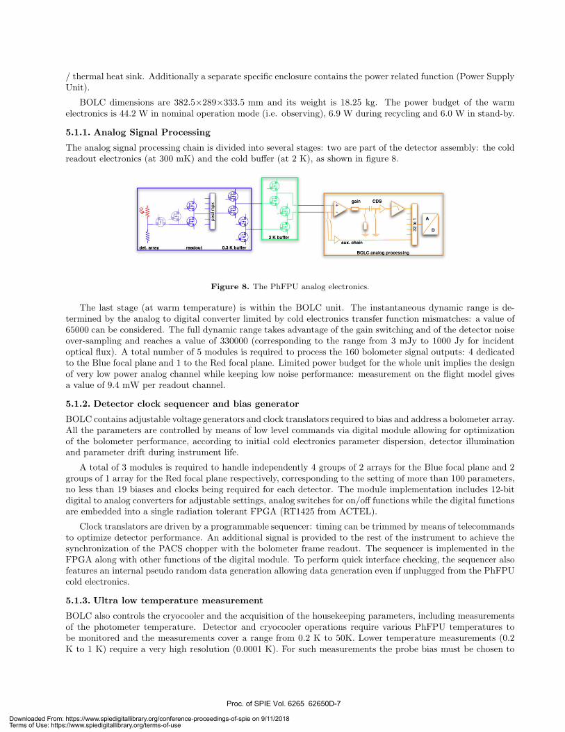
The analog signal processing chain is divided into several stages: two are part of the detector assembly: the coldreadout electronics (at 300 mK) and the cold buffer (at 2 K), as shown in figure 8.
Figure 8. The PhFPU analog electronics.
The last stage (at warm temperature) is within the BOLC unit. The instantaneous dynamic range is de-termined by the analog to digital converter limited by cold electronics transfer function mismatches: a value of65000 can be considered. The full dynamic range takes advantage of the gain switching and of the detector noiseover-sampling and reaches a value of 330000 (corresponding to the range from 3 mJy to 1000 Jy for incidentoptical flux). A total number of 5 modules is required to process the 160 bolometer signal outputs: 4 dedicatedto the Blue focal plane and 1 to the Red focal plane. Limited power budget for the whole unit implies the designof very low power analog channel while keeping low noise performance: measurement on the flight model givesa value of 9.4 mW per readout channel.
5.1.2. Detector clock sequencer and bias generator
BOLC contains adjustable voltage generators and clock translators required to bias and address a bolometer array.All the parameters are controlled by means of low level commands via digital module allowing for optimizationof the bolometer performance, according to initial cold electronics parameter dispersion, detector illuminationand parameter drift during instrument life.
A total of 3 modules is required to handle independently 4 groups of 2 arrays for the Blue focal plane and 2groups of 1 array for the Red focal plane respectively, corresponding to the setting of more than 100 parameters,no less than 19 biases and clocks being required for each detector. The module implementation includes 12-bitdigital to analog converters for adjustable settings, analog switches for on/off functions while the digital functionsare embedded into a single radiation tolerant FPGA (RT1425 from ACTEL).
Clock translators are driven by a programmable sequencer: timing can be trimmed by means of telecommandsto optimize detector performance. An additional signal is provided to the rest of the instrument to achieve thesynchronization of the PACS chopper with the bolometer frame readout. The sequencer is implemented in theFPGA along with other functions of the digital module. To perform quick interface checking, the sequencer alsofeatures an internal pseudo random data generation allowing data generation even if unplugged from the PhFPUcold electronics.
5.1.3. Ultra low temperature measurement
BOLC also controls the cryocooler and the acquisition of the housekeeping parameters, including measurementsof the photometer temperature. Detector and cryocooler operations require various PhFPU temperatures tobe monitored and the measurements cover a range from 0.2 K to 50K. Lower temperature measurements (0.2K to 1 K) require a very high resolution (0.0001 K). For such measurements the probe bias must be chosen to
Proc. of SPIE Vol. 6265 62650D-7
Downloaded From: https://www.spiedigitallibrary.org/conference-proceedings-of-spie on 9/11/2018Terms of Use: https://www.spiedigitallibrary.org/terms-of-use

R BOLO
VBIAS
VBOLO
R REF
R BOLO
R BOLO R REF+
R BOLO
R BOLO R REF+VBOLO VBIAS
RR ratio =
=
Figure 9. Electrical setup of the bolometric bridge for a single pixel (left). Definition of the RR ratio and the correspondingexpression for VBOLO (right).
maximize sensitivity and to limit self heating (Pprobe < 1 nW). Even higher resolutions (10 µK) can be achievedby accumulating samples over one second.
5.1.4. SpaceWire digital interface
The digital module handles analog module communications as well as external communication with the PACSwarm electronics based on a single Command and Data interface running over the SpaceWire standard. TheSpaceWire core has been developed in order to optimize design integration. Thus all the digital functions of theBOLC unit have been embedded into a single radiation tolerant RT54SX32S FPGA from ACTEL .
5.1.5. Redundancy
Standard safety considerations have been taken into account in order to deal with electronics failures: singlepoint failures are avoided and failure propagations are minimized. Unit internal redundancy relies on bothcold and warm redundancies: analog functions are shared into 6 independent modules each being devotedto a bolometer sub-assembly (warm redundancy) while digital functions (clock sequencer, interfaces to PACSinstrument, internal interfaces to analog functions) are doubled (cold redundancy). Therefore a failure at analogelectronics level is limited to a portion of the field of view and recovery from a failure in digital electronics issimply achieved by switching from main to redundant module.
6. PERFORMANCES OF THE PHOTOMETER FOCAL PLANE UNIT
Delivery of the Photometer to the PACS consortium at the Max Planck Institute for Extraterrestrial Physics(Germany) is scheduled for June 2006. The results presented in this section were obtained in CEA Saclayduring the first quarter of 2006 while preparing for the calibration campaign and deal mainly with performanceoptimizations.
6.1. Measuring RR ratios
The bolometric signal, VBOLO, is set at the middle point of a voltage divider, also called bolometric bridge.It consists of a bolometer resistor RBOLO and a reference resistor RREF . Figure 9 shows the electrical setupof the bolometric bridge and the definition of the RR ratio. Both resistors are strictly identical∗, however thebolometer’s temperature, hence its impedance, is allowed to fluctuate with the pixel temperature whereas thereference resistor is in thermal contact with the inter pixel wall which acts as the 300 mK heat sink (figure 3). Inthis configuration the reference resistor is used as a current source for the bolometer and prevents any burnoutphenomenon. Note that typical voltages applied across the resistors are of the order of a few Volts which induceselectric field effects in the conduction process (impedance decreases with applied voltage).
While most bolometers can be fully characterized by measuring their load curves, we rather use RR ratios todetermine the state of the bolometric bridge. Indeed the bolometers are multiplexed and each array contains 256bolometers mounted in parallel so we cannot measure the current flowing through each bolometer individually.
∗Same doping, same size (40×600 µm) and impedance of about 0.7 TΩ at 300 mK
Proc. of SPIE Vol. 6265 62650D-8
Downloaded From: https://www.spiedigitallibrary.org/conference-proceedings-of-spie on 9/11/2018Terms of Use: https://www.spiedigitallibrary.org/terms-of-use

Figure 10. Median RR ratios of a single array plotted versus voltage bias for different background fluxes (left) and thecorresponding VBOLO values (right). Top curves corresponds to 0 pW background and bottom curves to 6 pW.
Moreover the 300 mK reference resistor impedance varies with the applied bias due to electric field effects andit cannot be considered as an actual load resistor.
RR ratios are obtained from static measurements with a stable and thermalized black body illuminatingthe whole focal plane. We record the 40 Hz-sampled signal of each of the 2560 bolometers for 3 minutes indifferent bias/background flux configurations. In fact each of these configurations requires a different tuning ofthe detectors to avoid saturation of the signal. Reconstructing RR ratios by taking into account the differentoffsets and gains of the electronics chain provides us with absolute measurements of the bolometric bridge andmakes data obtained in very different conditions comparable. The computation of RR ratios played an importantrole in understanding the functioning of the bolometer arrays. RR ratios and their corresponding VBOLO valuesare plotted in figure 10. RR ratios can be interpreted as a competition between the reference and the bolometricresistors and reflect the balance or rather the unbalance of the bolometric bridge.
RR ratio measurements provide us with a large and valuable amount of information. For instance detectorresponsivity can be derived from the data presented here as described in section 6.2. Moreover we made anextensive use of these ratios to predict the different voltages necessary to power up the detectors†. Indeed themiddle points being quite dispersed, it is crucial to fine-tune the detectors to ensure all pixels fit in the dynamicsof the ADC.
6.2. Responsivity measurements and non-linearity
The responsivity is usually measured by modulating the incident flux with a chopper, the responsivity is thenthe ratio of the signal amplitude to the flux modulation amplitude. It is expressed in V/W. In our case since RRratios are reconstructed for different biases and background fluxes we compute ∂Signal/∂F lux for each pixeland for each flux and bias. Figure 11 shows a responsivity map of the Blue focal plane for a bias of 2.2 V witha background flux of 2 pW/pixel. The responsivity is about 4×10¹⁰ V/W and is quite homogeneous over thewhole focal plane.
Table 4 presents the average responsivity of the Blue focal plane for fluxes in the range 0 to 7 pW/pixel‡
along with its associated deviation. It shows only a slight non-linearity over this background flux range.
6.3. Spectral noise density and bandpass cutoff frequency
PACS bolometers exhibit noise levels two orders of magnitude higher than “usual” bolometers. This is mainlydue to the MOS cold readout electronics located at 300 mK but also to their impedance close to 1 TΩ. We
†There is a set of 19 inter-dependant voltages necessary to tune the bolometers of a single array‡We expect a background flux from the telescope between 1 and 6 pW/pixel.
Proc. of SPIE Vol. 6265 62650D-9
Downloaded From: https://www.spiedigitallibrary.org/conference-proceedings-of-spie on 9/11/2018Terms of Use: https://www.spiedigitallibrary.org/terms-of-use

II
U a.
Figure 11. Responsivity map of the Blue focal plane for a backgroundflux of 2 pW/pixel and a bias of 2.2 V.
Background Mean Resp. σFlux (pW/pix) (×1010 V/W) (%)
0 4.20 20.541 4.18 20.492 4.15 20.443 4.13 20.394 4.11 20.345 4.08 20.296 4.06 20.247 4.03 20.18
Table 4. Mean responsivities of the Blue focalplane measured in static mode for different fluxesand its associated relative dispersions.
actually measure noise levels at 3 Hz of about 7 µV.Hz−1/2 on the Blue focal plane and 18 µV.Hz−1/2 on the Redone. Figure 12 shows the spectral noise density extracted from a 3 hours measurement as well as a histogramof noise levels measured at 3 Hz. The spectrum was obtained by coadding spectra of 4-minutes sub-samples todecrease the statistical fluctuations. Moreover 256 spectra from pixels of the same array have been averaged toobtain the final spectrum representative of the whole array.
We distinguish 3 domains in this spectrum: (1) the low frequency region (fknee <0.5 Hz) concentratesmost of the energy and is responsible for signal drifts, (2) the operational regime between 0.5 and 5 Hz which isdominated by photon noise and (3) the white noise filtered by the bolometers electrical time constant (τ ∼60 ms).Additional bandpass tests confirmed the 5 Hz value for the electrical bandpass cutoff frequency§ and revealed athermometric time constant of 20 ms. These time constants can possibly be lowered by increasing the bias.
Figure 12. Average noise spectrum of 256 pixels from the same array (right). The histogram showing the noise dispersionon the Blue and Red focal planes.
6.4. Sensitivity measurements
In the sub-millimeter regime, the sensitivity is usually expressed as a NEP (Noise Equivalent Power) and isdefined as the ratio of the noise level by the responsivity. We adopt this definition and we find an optimal NEPof 2× 10⁻¹⁶ W/
√Hz at 90 µm and 3.5× 10⁻¹⁶ W/
√Hz at 160 µm for a bias of 2 Volts at a background flux of
2 pW/pixel.
§The bandpass cutoff frequency is defined as the modulation frequency at which the signal is attenuated by 3 dB.
Proc. of SPIE Vol. 6265 62650D-10
Downloaded From: https://www.spiedigitallibrary.org/conference-proceedings-of-spie on 9/11/2018Terms of Use: https://www.spiedigitallibrary.org/terms-of-use

Again, these results were derived from the data presented in section 6.1. The 3 minutes samples recorded ineach configuration were used to compute noise levels at 3 Hz and responsivities were derived from ∂Signal/∂F lux.Figure 13 presents NEP values for fluxes between 1 and 5 pW/pixel as a function of the applied bias. The optimumNEP is reached for a bias around 2 V independently of the background flux. At low biases the Joule dissipationis small and the bolometers are too cold, resulting in a very high impedance and thus high noise levels. At higherbiases, bolometers are heated up by Joule dissipation which decreases significantly the impedance and thus theresponsivity.
Figure 13. Measured median NEP obtained in static setup (without chopping) for background fluxes of 1 to 5 pW/pixelfrom bottom to top (left); the corresponding histogram showing the dispersion of NEP on the whole PhFPU for abackground of 2 pW/pixel and a bias of 2 V (right).
7. CONCLUSION AND FUTURE DEVELOPMENTS
The development of the bolometers for the Herschel/PACS instrument demonstrates that it is now possible tobuild fairly large (> 1000 pixels) focal planes based on filled arrays. The grid + resonant cavity concept works,the science requirements on the Blue focal plane have been reached and we will improve the performances of theRed focal plane before delivery to the PACS consortium.
The future of this type of bolometers looks very bright. We have already started a number of developmentsthat will make use of these detectors in the sub-mm and millimeter wavelength ranges, opening the possibilityof wide field imaging in these spectral domains. The two main axes of development are (1) to redesign thepackaging of the arrays to make them 4-side buttable, opening the way for very large focal planes of bolometers,and (2) to adapt the grid + cavity concept for absorption at longer wavelength.
Table 5 lists the different projects in terms of spectral range, size of focal planes, and telescopes.
Table 5. On-going developments of filled arrays of bolometers.
Name Spectral range Focal plane Telescope Operational inP-ARTEMIS 2 channels 200 + 450 µm 1 array per channel KOSMA + Chile 2006
PILOT 2 channels 240 + 550 µm 2x2 arrays per channel balloon 2009ARTEMIS-1 3 bands 200 – 350 – 450 µm 4x4 arrays APEX 2009ARTEMIS-2 3 bands 0.85 – 1.2 – 2 mm 4x4 arrays open (IRAM...) 2010
The adaptation of the bolometers to longer wavelengths is simply a tuning of the depth of the resonant cavity,in order to keep it at a quarter of the wavelength of interest. This tuning can be done in several ways: keeping
Proc. of SPIE Vol. 6265 62650D-11
Downloaded From: https://www.spiedigitallibrary.org/conference-proceedings-of-spie on 9/11/2018Terms of Use: https://www.spiedigitallibrary.org/terms-of-use
Dual—bum 450 urn .oan map of lupitir (P—Arteml./XOSMA)150
- 5 io
0
—5. io
50 100 150
the same cavity and putting a dielectric layer with the proper thickness on top of the pixel, inserting a spacer inbetween the absorbing grid and the reflector to adjust the depth of the cavity, or a mix of these two methods.This adaptation to longer wavelengths is presented in ref. 6, and the ARTEMIS project is presented in greaterdetails in ref. 7.
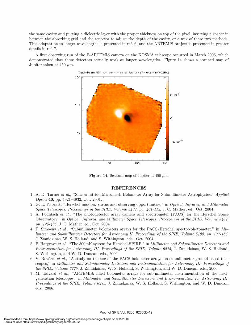
A first observing run of the P-ARTEMIS camera on the KOSMA telescope occurred in March 2006, whichdemonstrated that these detectors actually work at longer wavelengths. Figure 14 shows a scanned map ofJupiter taken at 450 µm.
Figure 14. Scanned map of Jupiter at 450 µm.
REFERENCES
1. A. D. Turner et al., “Silicon nitride Micromesh Bolometer Array for Submillimeter Astrophysics,” Applied
Optics 40, pp. 4921–4932, Oct. 2001.2. G. L. Pilbratt, “Herschel mission: status and observing opportunities,” in Optical, Infrared, and Millimeter
Space Telescopes. Proceedings of the SPIE, Volume 5487, pp. 401-412, J. C. Mather, ed., Oct. 2004.3. A. Poglitsch et al., “The photodetector array camera and spectrometer (PACS) for the Herschel Space
Observatory,” in Optical, Infrared, and Millimeter Space Telescopes. Proceedings of the SPIE, Volume 5487,
pp. 425-436, J. C. Mather, ed., Oct. 2004.4. F. Simoens et al., “Submillimeter bolometers arrays for the PACS/Herschel spectro-photometer,” in Mil-
limeter and Submillimeter Detectors for Astronomy II. Proceedings of the SPIE, Volume 5498, pp. 177-186,J. Zmuidzinas, W. S. Holland, and S. Withington, eds., Oct. 2004.
5. P. Hargrave et al., “The 300mK system for Herschel-SPIRE,” in Millimeter and Submillimeter Detectors and
Instrumentation for Astronomy III. Proceedings of the SPIE, Volume 6275, J. Zmuidzinas, W. S. Holland,S. Withington, and W. D. Duncan, eds., 2006.
6. V. Reveret et al., “A study on the use of the PACS bolometer arrays on submillimeter ground-based tele-scopes,” in Millimeter and Submillimeter Detectors and Instrumentation for Astronomy III. Proceedings of
the SPIE, Volume 6275, J. Zmuidzinas, W. S. Holland, S. Withington, and W. D. Duncan, eds., 2006.7. M. Talvard et al., “ARTEMIS: filled bolometer arrays for sub-millimeter instrumentation of the next-
generation telescopes,” in Millimeter and Submillimeter Detectors and Instrumentation for Astronomy III.
Proceedings of the SPIE, Volume 6275, J. Zmuidzinas, W. S. Holland, S. Withington, and W. D. Duncan,eds., 2006.
Proc. of SPIE Vol. 6265 62650D-12
Downloaded From: https://www.spiedigitallibrary.org/conference-proceedings-of-spie on 9/11/2018Terms of Use: https://www.spiedigitallibrary.org/terms-of-use