the high performance graphics subsystem
TRANSCRIPT

^'^Ad
iinicom GrapkicsCorporatloa
J^l / I 'r...
fj M___ N I ==00,11 ..rD" / r'4TM
The High Performance
The OMNI 2400 GDS incorporates both high performance raster graphics and image proces-sing in a single system. Additionally, this system supports multiple, independent graphics channels or true color capabilities.
The OMNI 2400 GDS is available as a traditional packaged system with DEC compatible parallel inter-faces or as a board level system with an Intel MULTIBUS II system bus interface. By combining sophisticated graphics system design techniques with a high performance public bus structure, the OMNI 2400 GDS provides an opportunity for system devel-opers to integrate high performance vector and image graphics with powerful computing platforms on the same system bus.
The OMNI 2400 GDS is a modular, multiple board system which conforms to the MULTIBUS II 6U x 220mm form factor. Two system interfaces are provided P1 - the standard IPSB interface using the message passing protocol, and P2 - the interface to the GBX-11 bus, passing control and data signals unique to the OMNI 2400 GDS (see figure 1).
A minimum OMNI 2400 GDS system consists of two modules, the Graphics Control Processor (GCP) and the Graphics Output System (GOS). This configuration provides seven mips bit slice geometry processor (GCP), a seven rntlops floating point coprocessor, a proprietary vector coprocessor, a graphic input device controller, four planes of 1280 by 1024 display memory, a hardware cursor, and a 60 Hz non-interlaced (112 MHz) video output channel.
System func- tionality can be en- hanced through the ..
addition of other corn- j, ..4 .• .-
plementary modules , •
including a Graphics Memory System (GMS) and a Graphics Data
Base Manager (GDM). -
The OMNI 2400 GMS pro- -.
vides 8 bit planes (optionally .. .
double buffered) per board and allows the expansion of the system to use up to 48 ' . , • '•
5''
bit planes. Each GMS can also ,. ''
be configured to drive an inde- pendent monitor. Thus the OMNI 2400 GDS can be used as a true color system or as a multi-channel device, The OMNI 2400 GDM provides the user with high speed display list pro-cessing and level 2C+ GKS functionality, via Omnicomp's proprietary OMNIKERNEL System (OKS) firmware, in addition to advanced imaging functionality resident on the Graphics Control Processor module.
V "S
OEM Graphics Subsystem
ri

Graphics Corporation
011JIf Ij Omni 4D73 UJJ ^^j TM
Graphics Control Processor
The Graphics Control Processor (GCP) is a graphic drawing engine, an image manager and a geometry pro-cessor. All GCP functions are controlled by a highly parallel seven mips AMD 29116 based bit slice processor which uses a 72 bit wide microword instruc-tion. A seven mflops floating point co- - processor, the AMD 29325 floating point ALU, communicates with the bit slice processor through a dual ported 8 KByte scratch RAM.
The bit slice processor provides sig-nificant flexibility in the application functionality of the OMNI 2400 GDS. This processing power is easily ap-plied to both geometry processing and digital filtering, The design of the microcode takes full advantage of this resource by providing commands for two and three dimensional vector and polygon oriented functions as well as image analysis and processing opera-tions. In addition to vector and polygon draw, transform, and zoom operations; a convolution function provides digital image filters including Laplace, high, and low pass. Spatial and logical operations are also provided.
The GCP communicates with the host CPU through DEC compatible parallel interfaces or through the iPSB inter-face. Efficient data transmission is maintained with both data channels by using buffered fifo's. Also included within the GCP module is a peripheral coprocessor which supports four RS-232 serial data ports. This Intel 80188 based coprocessor provides a direct link between a graphics locator device, such as a mouse or digitizer, and the graphics cursor generator. This offloads the cursor positioning responsi-bilities from the drawing engine.
For applications which require a variety of rapidly generated bit mapped text fonts, the GCP contains 40 KBytes of high speed memory which may be downloaded with custom text fonts. A typical 15 pixel wide by 20 pixel high bit mapped text character is drawn in less than 10 microseconds. Bit mapped text may be clipped, pixel by pixel, to an arbitrary screen viewport with no performance penalty.
The primary function of the GCP is to execute drawing and image manipu-lation commands which are passed to it either by the GDM or by the host CPU. The GCP is capable of proces-
sing drawing primitives specified in both screen and world coordinate systems. Those drawing primitives which are specified in the world coor-dinate system are first converted to screen coordinates by the floating point coprocessor. The conversion process consists of a general geometric trans-formation, followed by a clipping opera-tion and finally a window to viewport mapping. The bit slice processor con-verts screen coordinate drawing primi-tives and raster image data into a series of data words and control sig-nals used by the vector coprocessor.
The 14 MHz vector coprocessor uti-lizes proprietary logic developed by Omnicomp Graphics Corporation. This coprocessor is capable of generating vectors of any orientation at the rate of one pixel per 70 ns and bit mapped text at ten microseconds per character.
In order to de-couple the vector coprocessor from the system frame buffer, a 20 pixel cache is employed. The pixel cache is organized as a 5 pixel by 4 pixel array. The entire contents of the pixel cache can be writ-ten to an arbitrary location within the frame buffer in a single frame buffer memory cycle of 430 ns.
Figure 1: The OMNI 2400 GDS system consists of a minimum of two modules: the graphics control pro-cessor (GCP) and the graphics output system (GOS) module. Added functionality can be ob- tained by using a graphics memory system (GMS) module and a graphics database manager (GDM).
PSE
DEC MOUSE RGB COMPATIBLE KEYBOARD ANALOG
PARALLEL VIDEO INTERFACE

Because of the 5 by 4 pixel cache and the pro-prietary coprocessors, the OMNI 2400 GDS can sustain a throughput of over 200,000 forty pixel vectors per second. This unique architecture mini-mizes the number of frame buffer accesses re-quired for typical drawing operations and facilities highly efficient execution of all graphic primitives. - Fat lines, patterned fills, patterned lines, irregular J' "' fills, polymarkers, bit mapped text and paint brush style strokes are examples of operations which benefit from this drawing efficiency (see figure 3).
Graphics Output System
The Graphics Output Sys module provides the video frame buffer and video output functions required by the OMNI 2400 GDS. Each system contains a single GOS module which allows for the attachment of one to three independent monitors. The three independent RGB video channels will support a single GMS per RGB channel. The overlays may be split
up among the different heads in any fashion, including the display of a single overlay plane on more than one head. The GOS may also be configured to support a true color con-
figuration in which the three video
r r f channels are used as separate R, channels. G. and B cha
rI The GOS module ' contains four planes of
U 1f2 I frame buffer memory. - Video data generated by these planes may
- - - - overlay the video data received from the op-tional GMS modules.
• -r
The GOS multiplexes
- the data bits it receives • from the GMS into a
- . . 112 MHz video signal. The video data stream
• is then routed to the color palettes, which
• . , . provide the color look up and digital to
F . I analog signal conver- sion functions. When
configured with a GMS, the OMNI 2400 GDS provides a palette of 16.7 million colors (see figure 5). A separate overlay color look up table is used to control how the overlay video data affects the primary video signal. Systems configured without a GMS module use the GOS
Figure 2: All GCP functions are con-trolled by an AMD 29116-based bit-slice processor. The GCP com-municates with the host through either a DEC-com-patible interface or the MUIJIBUS Il's iPSB.
Figure 3: If each pixel in the vector represented in (A) were drawn indi- vidually, 15 memory cycles would be required. By allowing simultaneous access of the two-dimen-sional regions of the frame buffer, only three memory cycles are required. If the text character represented in (B) were drawn using a pixel block transfer, a frame buffer that allows only scan-line access would require 12 memory cycles to complete the transfer, the GDS requires only six memory cycles.
'ARALLEL DOUBLE BUFFER SERIAL DOUBLE BUFFER
frame buffer to provide a 16 color display.
In order to simplify the use of the graphic cursor, the GOS provides a hardware generated matrix and cross-hair cursor. By generating the graphic cursor on the fly rather than by drawing it into a frame buffer plane, any inter-ference between frame buffer data and the cursor is removed. The cursor video signal is routed through the overlay look up table to allow the cursor display characteristics to be adjusted.
Graphics Memory System
The graphic memory system (GMS) module provides up to 1280 x 1024 x 16 frame buffer memory in multiple configurations. By employing dual ported video RAM in the GMS design rather than conventional DRAM, a more efficient frame buffer memory organization is made possible. By combining three GMS modules to-gether, a 48 plane, true color, double buffered system can be configured. In addition, each GMS may have its eight plane buffer as additional overlay planes; as a 16 pixel memory
in conjunction with the first buffer, where any eight contiguous planes can be displayed; or as a 1280 x 2048 x 8 image memory.
The frame buffer implementation, used by the OMNI 2400 GDS maximizes the frame buffer input bandwidth and allows multiple scanlines to be accessed simultaneously. This results from the fact that most drawing operations exe-cute with fewer frame buffer accesses when small two dimensional regions of the frame buffer may be accessed at once rather than by a single scan line. The OMNI 2400 GDS frame buffer memory is organized as 256 rows by 256 columns of 5 pixel by 4 pixel words. This memory organization is possible due to the dual ported video RAM's high serial output port band-width, which allows a narrow frame buffer word to provide the required frame buffer output bandwidth.
Physically, each 5 by 4 pixel word consists of 20 pixels which share a common memory address. In order to further reduce the number of frame buffer accesses, the frame buffer design allows the contents of the pixel cache to be written to any location within the frame buffer in a single
memory cycle, without regard to the physical frame buffer word boundaries. Each pixel within the frame buffer cell is individually addressable. A two-dimen-sional barrel shifter is used to com-pensate for misalignment between the contents of the pixel cache and the fixed cell boundaries of the frame buffer.
Each GMS contains five proprietary gate arrays for direct pixel processing and rapid pixel transfer of data from the iPSB. Coupled with multipliers, these provide the Single Instruction Multiple Data (SIMD) architecture which provides up to 80 mips of per-formance per GMS module. Up to five megabytes of data per second can be transferred to and from the iPSB per second. This unique design allows the OMNI 2400 GDS to move data from local bus storage or local disk storage at animation speeds.
The GOS/GMS architecture also permits hardware zoom and pan of the display buffers.
Serial Versus Parallel
Another form of block pixel transfer is used by the GMS to transfer data from one set of frame buffer planes to
ixel in nted in
I-
ry cycles By us imen-
he frame memory
if the esented
U
a r, a allows ess memory
the
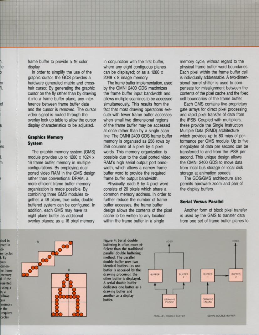
Figure 4: Serial double buffering is often more ef-ficient than the traditional parallel double buffering method. The parallel double buffer uses two identical buffers—as one buffer is accessed by the drawing processor, the other buffer is displayed. A serial double buffer dedicates one buffer as a drawing buffer and another as a display buffer.

another, thus providing a serial double buffering capability. Double buffering is used to delay the visual effects of drawing operations until the drawing is complete. Serial double buffering, as it is employed by the OMNI 2400 GDS, is often significantly more effi-cient than the traditional parallel double buffering method. The parallel double buffer employs two identical buffers. As one buffer is accessed by the drawing processor, the other buffer is displayed. When the drawing is complete the original drawing buffer becomes the display buffer, and the original display buffer becomes the current drawing buffer. The parallel double buffer is convenient if the entire buffer content is regenerated before each buffer swap. If, on the other hand, only a portion of the buffer content is modified, such as in a multiple window display, the parallel double buffer is much less convenient. Because the most recent modifica-tions to the display buffer are not reflected in the current drawing buffer, they must be duplicated in the draw-ing buffer before the current drawing activity may proceed. This redundant activity significantly affects both system
performance and operating overhead (see figure 4).
A serial double buffer on the other hand dedicates one buffer as a draw-ing buffer and another as a display buffer. As a drawing is completed the contents of the drawing buffer are transferred into the display buffer. The OMNI 2400 GDS performs this block transfer in a single video frame time of 16.667 milliseconds. Each pixel is moved from the drawing buffer to the display buffer just after the display pixel is sent to the screen. This results in an apparently instant change in the display. By employing a dedicated drawing buffer, the ineffi-ciencies of the traditional double buf-fering method are removed. Because the data transfer from the drawing buffer to the display buffer does not impede the drawing process, the double buffer may be made transparent by constantly enabling the transfer. The OMNI 2400 GDS supports parallel double buffering as well.
Graphics Database Manager
The GDM module is an Intel 80386/80387 based CPU and memory board and is configured as a back-
end processor. This allows the bit slice drawing processor to scan the incoming command stream and execute any commands targeted for it. The GDM connects to other system modules via the iPSB bus interface. A 64 Kbyte memory cache is used to allow the 80386/80387 to run at 16 MHz with no wait states. A large display list store, consisting of up to 16 Mbytes of memory, is connected directly to the 32 bit wide memory cache.
The display list operations executed by the GDM correspond directly to standard host based GKS subroutine calls. By using the same OMNI*KERNEL System firmware as other Omnicomp products, the philosophy of providing upward compatibility throughout its family of graphics systems has been retained. Thus, the systems integrator has a price/performance range of soft-ware compatible graphics devices with which to address his marketplace requirements. This firmware is written entirely in 80386 assembly language and executes in a stand alone fashion, with no intervening operating system. The responsibilities of the GDM are to manage the data base and graphic attribute control functions.
Figure 5: The graphics out-put system (GOS) module contains four planes of frame buffer memory, an overlay look-up table and up to three channels of video interface. Systems configured without a graphics memory system (GMS) module use the GOS frame buffer to pro-vide either a double buf-fered sixteen-color display.
Designed for the OEM
The modular nature of the OMNI 2400 GDS allows system expansion and enhancement to occur in an incremental manner. The overall design philosophy behind the OMNI 2400 GDS is to pro-vide a family of board level components which may be combined to provide a standard set of high performance graphic display functions.
Graphics display subsystems must be designed to meet the widely varying re-quirements of OEM's and system inte-
grators. Modular flexibility allows those requirements to be met without the cus-tomer purchasing more features than necessary. A modular design also enables the manufacturing company to evolve the subsystem; incorporating new semiconductor innovations, keeping it price/performance competitive. The OMNI 2400 GDS was conceived to meet the needs of a broad spectrum of appli-cations. As such, it must remain both a physical product and a design concept. As it evolves over the coming years, most of the currently used components
will be designed out in favor of parts providing denser integration, more per-formance and better economics. What will remain is the concept of what its functionality must be, the algorithms used to provide that functionality and the buses and pathways linking all of its parts internally and externally. The modularity, the security of standards, and the growth path gained from confor-mance to MULTIBUS II (IEEE P1296), ISO GKS and other accepted design ap-proaches will allow these changes to be well thought out and manageable.
Specifications:
Display Characteristics: 1280 x 1024 Display Resolution 60 Hz Non-interlaced or 30 Hz Interlaced Hardware Screen Clipping Hardware Matrix and Crosshair Cursors 4 Overlay Planes 1, 2 or 3 Displays
Display Memory Configurations: 4 Planes 8 Planes 8 Planes Double Buffered 2 x 8 Planes - Twin Heads 3 x 8 Planes - Triple Heads or True Color 2 x 8 Planes - Twin Heads, Double Buffered 3 x 8 Planes - Triple Heads or True Color, Double Buffered
Display List Memory: 1. 4 or 16 Mbytes
Multiple Processors: GCP: Geometry Processor - 29116 Bit Slice
Floating Point Coprocessor - 29325 FPP Primitive Coprocessor - Discreet TTL Peripheral Coprocessor - 80188
GMS: Five Pixel Processors - proprietary gate arrays and ADSP-110 multiplier
GOS: Frame Buffer Control Processor- 14 MHz Bit Slice
Features
J Modular Configurations
U MULTIBUS II iPSB and DR11-W Interfaces
U High Speed 2D and 3D Geometry Processing
U GKS Display List Processor/Manager
U Highly Parallel, Pipelined Architecture
U Non-destructive Overlay Planes
U Hardware Cursor
U Region of Interest Processing
U Serial Double Buffering
U Image Processing Commands
U Monochrome to True Color
Very Fast Pixel Draws: Vectors: Up to 10 Megapixels per Second Fills: Up to 40 Megapixels per Second BLT: 20 Megapixels per Second
......J Very High Speed Bit-Mapped Characters
Omnicomp Graphics Corporation
Omnicvnip Graphics (UK) Ltd.
GDM: Display List Processor - 80386 Floating Point Coprocessor - 80387
Power Requirements: 310 Watts 110 VAC - typical
Optimizing Computer Graphics.. . by Design.
1734 West Belt North, Houston, Texas 77043 713/464-2990 • Telex 285801 OMNICO UR • Fax 7131827-7540
DEC. DRI1.W. DRVI1.WA. are trademarks of Digital Equipment Corporation 80386 80387, 80188, MULTIBUS Ii. Intel, iP5B are trademarks of Intel Corporation. AMD. 29116 and 29325 are trademarks of Advanced Micro Devices. ACRIC is a trademark of Hitachi Corporation OMNI 2400 GOS, OMNI 2400 GDS, OMN1 2400 GMS, OMN 2400 GCP. 0MM 2400 GOM, GBX-ii and OMNIKERNEL are trademarks of Omnicomp Graphics Corporation
CopyrigP* Omnicomp GraIncs Corpor*ion. 1988
Host Interfaces: MULTIBUS II iPSB 16-Bit Parallel DMA (DRV11-WAIDR11-W)
Video: RS-343 ROB, Composite Available Pixel Clock: 112 MHz Non-interlaced
56 MHz Interlaced
Specifications subject to change without notice.
Printed n USA

Ol.Qfl 1000 GDC/O)*I 1200 GDCTH TECHNICAL OVERVIEW
The O!.flfl 100011200 Graphics Display Controllers (GDC) establish a new stan-dard in price performance, versatility and proven reliability. The OMNI 1000 GDC/OMNI 1200 GDC single board graphics controllers combine innovative en-gineering with efficient manufacturing management to provide unequaled cost effective solutions for graphics display requirements. The OMNI 1000 GDC/OMNI 1200 GDC are major advances in high performance GKS display graphics for ap-plications relating to the fields of mechanical and electronics design, AEC, cartography and geoseismic evaluation.
FEATURES
- Innovative design techniques provide high performance, reliability and low price in a single board
- OMNI*KERNEL System (OKS) firmware provides Draft ANSI and enhanced ISO GKS compatible functionality.
- Display resolution is firmware definable from 512 x 512 pixels to 1280 x 1024 pixels
- Image memory of 1024 x 1024 pixels or 2048 x 2048 pixels
- Instantaneous vector drawing speed of 1.5 million eight bit pixels per second
- 256 colors simultaneously displayed from a palette of 4096 or 16.7 million colors
- Multiprocessor design augmented by VLSI graphics controller
- On-board display list processing
- Firmware support for a wide variety of graphics input devices and peripherals
INNOVATIVE FLEXIBILITY AND ECONOMICAL PERFORMANCE
By exercising engineering innovation, incorporating public design standards and utilizing cost effective semiconductor technology, Omnicomp can offer the user a superior price performance value. The OMNI 1000 GDC/OMNI 1200 GDC in-corporate the reliability of single board packaging, the adaptability of com-plete bus independence, the performance of a firmware encoded instruction set, ISO GKS Standard compatibility and a distributive multiprocessor architecture.
(C) Copyright Otnnicomp Graphics Corporation, 1987, 1988
1

Single Board Reliability
Many mechanical connectors, a major cause of electronics system failures, have been eliminated by designing the products as single boards. In the event that service is required, replacing a single circuit board corrects any dif-ficulties.
Bus Independent
The OMNI 1000 GDC/OMNI 1200 GDC are designed to support parallel communica-tions with most computers at speeds of one million bytes per second. DMA in-terfaces are available for UNIBUS, Qbus, MULTIBUS, VME as well as the primary buses for other popular computer systems. High speed parallel I/O interfaces are also available for the Intel MULTIBUS iSBX, IBM bus and IBM PS-2 micro-channel. Serial RS 232-2 communications at speeds up to 19.2 Kilobaud are supported.
Distributive Multiprocessor Architecture
The architecture of the OMNI 1000 GDC/OMNI 1200 GDC optimizes graphics throughput by utilizing both general and special purpose microprocessors to accomplish different tasks. A general purpose 16-bit microprocessor manages generalized I/O, processes display list segments and executes OKS firmware in-structions. A floating point numeric co-processor accelerates all arithmetic operations. A specialized I/O processor manages bulk pixel transfers and con-trols DMA operations. A VLSI graphics controller manages all operations in-volving image memory.
Flicker-Free Interlaced Display
The OMNI 1000 GDC/OMNI 1200 GDC feature 1024 x 1024 display resolution at 34Hz interlaced refresh rate to provide flicker-free operation with a low cost monitor. Under firmware control the OMNI 1000 GDC/OMNI 1200 GDC can also operate in a non-interlaced mode at 1024 x 768 or lower resolution.
COMPLETE SUPPORT REDUCES APPLICATION IMPLEMENTATION EFFORT
Even the most advanced computer hardware is of limited utility until properly integrated with complementary hardware and application software. Omnicomp recognizes that the Customer's investment in integration and application software is important. A complete support library, detailed documentation, custom service and a broad range of available interfaces minimize any integra-tion and application development expense with the OMNI 1000 GDC/OMNI 1200 GDC.
(C) Copyright Omnicomp Graphics Corporation, 1987, 1988
2

OMNI*KERNEL SYSTEM
An important feature of the OMNI 1000 GDC/OMNI 1200 GDC is the OKS firmware. OKS is a complete 2D graphics package, including functional compatibility with the ISO GKS Standard in firmware. Additionally, OKS includes extensions com-monly used in graphics applications, but not accommodated by GKS, such raster operations and planar Boolean operations. By providing firmware to perform all graphics computations external to the host computer, the OMNI 1000 GDC/OMNI 1200 GDC free host resources for applications. In most cases, graphics operations are performed more quickly than if the same task were ex- ecuted by the host computer. Address space is available for the addition of customer defined firmware instructions. Some of the categories of functionality provided by OKS are:
o SYSTEM CONTROL
o RASTER OPERATIONS
o SEGMENT MANIPULATION
o DATABASE OPERATIONS
o DISPLAY CONTROL
o ECHO OPERATIONS
o PLANE MANIPULATIONS
OKLIB
o PRIMITIVES
o SET/INQUIRE CURRENT ATTRIBUTES
o SET/INQUIRE SEGMENT ATTRIBUTES
o COLOR CONTROL
o WINDOW/VIEWPORT CONTROL
o REQUESTS
o SAMPLE DEVICE
All OKS operations are fully supported by OKLIB, a compact host graphics software library available in FORTRAN or C. Site specific licenses are avail-able for source, or object forms, of OKLIB.
CONFIGURATION FLEXIBILITY
The OMNI 1000 GDC/OMNI 1200 GDC is available as a stand-alone circuit board, table top system, or within a 19m rack mount chassis. Each OMNI 1000 GDC/OMNI 1200 GDC can be ordered to meet customer requirements regarding display resolution, image memory size and custom firmware.
TECHNICAL SPECIFICATIONS
System Processors 8086 General Purpose Processor (8MHz) 8087 Floating Point Processor (8MHz) 8089 I/O Processor
(C) Copyright Omnicomp Graphics Corporation, 1987, 1988
3
System Memory 256 Kilobytes of Display List 64 Kilobytes of OKS or Custom Firmware
Display List Capacity Segmented Architecture: 1024 Segments
4096 Primitives 32,768 Endpoints
Graphics Controller 7220 Graphics Display Controller, Cycle Time 167 ns
Image Memory 1024 x 1024, 8 Planes; or 2048 x 2048, 8 Planes
Host Interfaces 16 Bit Parallel Programmed I/O (DRV11 or DR11-C) 16 Bit Parallel DMA (DRV11-B or DR11-W) Serial RS-232C, Maximum 19.2 Kbaud
Display Interface RS-343 RGB Video, Composite Available
Local Device Interfaces Mouse, Data Tablet, Keyboard, Joystick, Thumbwheels, Trackball and Touch Screen
Cursor Non-destructive
Operating Environment Temperature: 50°F to 95°F (10°C to 35°C) Humidity: 10% to 90% Non-condensing Altitude: 8,000 Feet (2,400 Meters)
Power Requirements 90-132 VAC, 60 Hz ± 2% 180-264 VAC, 50 Hz ± 2% Consumption: Approximately 50 Watts
Physical Dimensions Table Top: 5 3/4" H x 19" W x 19' D, 21.5 lbs. Rack Mount: 5 1/2" H x 19" W x 22" D, 21 lbs. Circuit Board: 16" x 16"
OKLIB, OMNI*KERNEL, OKS, OHM! 1000 GDC and OHM! 1200 GDC are registered trademarks of Omnicomp Graphics Cor-poration. IJNJBUS, Qbus. DR11-C, DR114, ORV11 and DRV11-B are registered trademarks of Digital Equipment Cor-poration. MIJLTIBUS and ISBX are registered trademarks of Intel Corporation. IBM PC is a registered trademark of IBM Corporation. All specifications subject to change without notice. 2/26/88 -
(C) Copyright Omnicomp Graphics Corporat: 87, 1988
4