the memory hierarchy cs 740 24 january 2017
TRANSCRIPT
The Memory HierarchyCS 740
24 January 2017
Topics• Memories
• Cache design
CS 740 S’17– 2 –
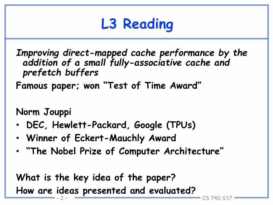
L3 Reading
Improving direct-mapped cache performance by the addition of a small fully-associative cache and prefetch buffers
Famous paper; won “Test of Time Award”
Norm Jouppi
• DEC, Hewlett-Packard, Google (TPUs)
• Winner of Eckert-Mauchly Award
• “The Nobel Prize of Computer Architecture”
What is the key idea of the paper?
How are ideas presented and evaluated?
CS 740 S’17– 3 –
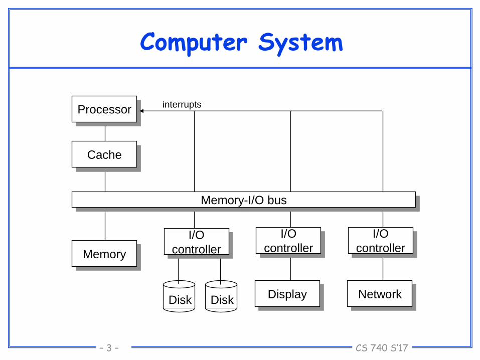
Computer System
diskDiskdiskDisk
Memory-I/O bus
Processor
Cache
Memory
I/O
controllerI/O
controller
I/O
controller
Display Network
interrupts

CS 740 S’17– 4 –
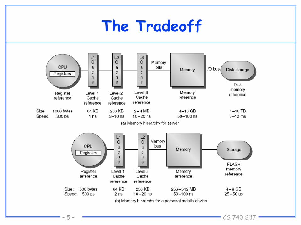
The Tradeoff
CPU
regs
C
a
c
h
e
Memory disk
size:
speed:
$/Mbyte:
block size:
608 B
1.4 ns
4 B
register
reference
L2-cache
reference
memory
reference
disk memory
reference
512kB -- 4MB
16.8 ns
$90/MB
16 B
128 MB
112 ns
$2-6/MB
4-8 KB
27GB
9 ms
$0.01/MB
larger, slower, cheaper
16 B 8 B 4 KB
cache virtual memory
C
a
c
h
e
128k B
4.2 ns
4 B
L1-cache
reference
(Numbers are for a 21264 at 700MHz)
CS 740 S’17– 5 –
The Tradeoff

CS 740 S’17– 6 –
The Performance Gap

CS 740 S’17– 7 –
Physical Size Affects Latency
7
Small Memory
CPU
Big Memory
CPU
Signals have further to travel Fan out to more locations

CS 740 S’17– 8 –
Why is bigger slower?
• Physics slows us down
• Racing the speed of light: (3.0x10^8m/s)• take recent Intel chip (Haswell-E 8C)
• how far can I go in a clock cycle @ 3 GHz?(3.0x10^8 m/s) / (3x10^9 cycles/s) = 0.1m/cycle
• for comparison: Haswell-E 8C is about 19mm = .019m across
• speed of light doesn’t directly limit speed, but its in ballpark
• Capacitance:• long wires have more capacitance
• either more powerful (bigger) transistors required, or slower
• signal propagation speed proportional to capacitance
• going “off chip” has an order of magnitude more capacitance

CS 740 S’17– 9 –
MEMORY

CS 740 S’17– 10 –
One-Transistor Dynamic RAM
10
TiN top electrode (VREF)
Ta2O5 dielectric
W bottomelectrode
polyword
line access transistor
1-T DRAM Cell
word
bit
access transistor
Storagecapacitor (FET gate,
trench, stack)
VREF

CS 740 S’17– 11 –
Modern DRAM Cell Structure
11
[Samsung, sub-70nm DRAM, 2004]
CS 740 S’17– 12 –
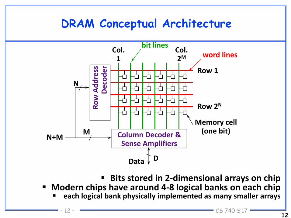
DRAM Conceptual Architecture
12
Ro
w A
dd
ress
D
eco
de
r
Col.1
Col.2M
Row 1
Row 2N
Column Decoder & Sense Amplifiers
M
N
N+M
bit linesword lines
Memory cell(one bit)
DData
Bits stored in 2-dimensional arrays on chip Modern chips have around 4-8 logical banks on each chip each logical bank physically implemented as many smaller arrays

CS 740 S’17– 13 –
DRAM Physical Layout
13
II. DRAM TECHNOLOGY AND ARCHITECTURE
DRAMs are commoditized high volume products which need to have very low manufacturing costs. This puts significant constraints on the technology and architecture. The three most important factors for cost are the cost of a wafer, the yield and the die area. Cost of a wafer can be kept low if a simple transistor process and few metal levels are used. Yield can be optimized by process optimization and by optimizing the amount of redundancy. Die area optimization is achieved by keeping the array efficiency (ratio of cell area to total die area) as high as possible. The optimum approach changes very little even when the cell area is shrunk significantly over generations. DRAMs today use a transistor process with few junction optimizations, poly-Si gates and relatively high threshold voltage to suppress leakage. This process is much less expensive than a logic process but also much lower performance. It requires higher operating voltages than both high performance and low active power logic processes. Keeping array efficiency constant requires shrinking the area of the logic circuits on a DRAM at the same rate as the cell area. This is difficult as it is easier to shrink the very regular pattern of the cells than lithographically more complex circuitry. In addition the increasing complexity of the interface requires more circuit area.
Figure 1 shows the floorplan of a typical modern DDR2 or DDR3 DRAM and an enlargement of the cell array. The eight array blocks correspond to the eight banks of the DRAM. Row logic to decode the row address, implement row redundancy and drive the master wordlines is placed between the banks. At the other edge of the banks column
logic includes column address decoding, column redundancy and drivers for the column select lines as well as the secondary sense-amplifiers which sense or drive the array master data lines. The center stripe contains all other logic: the data and control pads and interface, central control logic, voltage regulators and pumps of the power system and circuitry to support efficient manufacturing test. Circuitry and buses in the center stripe are usually shared between banks to save area. Concurrent operation of banks is therefore limited to that portion of an operation that takes place inside a bank. For example the delay between two activate commands to different banks is limited by the time it takes to decode commands and addresses and trigger the command at a bank. Interleaving of reads and writes from and to different banks is limited by data contention on the shared data bus in the center stripe. Operations inside different banks can take place concurrently; one bank can for example be activating or precharging a wordline while another bank is simultaneously streaming data.
The enlargement of a small part of an array block at the right side of Figure 1 shows the hierarchical structure of the array block. Hierarchical wordlines and array data lines which were first developed in the early 1990s [5], [6] are now used by all major DRAM vendors. Master wordlines, column select lines and master array data lines are the interface between the array block and the rest of the DRAM circuitry. Individual cells connect to local wordlines and bitlines, bitlines are sensed or driven by bitline sense-amplifiers which connect to column select lines and local array data lines. The circuitry making the connection between local lines and master lines is placed in the local wordline driver stripe and bitline sense-amplifier stripe
Row logic Column logic
Serializer and driver (begin of write data bus)
Buffer
1:8
Control logicSub-array
Center stripe
column select line (M3 - Al) master array data lines (M3 - Al)
local array data lines
master wordline (M2 - Al)
local wordline (gate poly)
bitlines (M1 - W)
local wordline driver stripe
bitline sense-amplifier stripe
Array block
(bold line)
Figure 1. Physical floorplan of a DRAM. A DRAM actually contains a very large number of small DRAMs called sub-arrays.
364
[ Vogelsang, MICRO-2010 ]

CS 740 S’17– 14 –
DRAM Operation
Three steps in read/write access to a given bank
• Precharge• Row access (RAS)• Column access (CAS)
Each step has a latency of around 10ns in modern DRAMs
Various DRAM standards (DDR, RDRAM) have different ways of encoding the signals for transmission to the DRAM, but all share same core architecture
14

CS 740 S’17– 15 –
DRAM Operation
Three steps in read/write access to a given bank
• Precharge• charges bit lines to known value, required before next row
access
• Row access (RAS)• Column access (CAS)
Each step has a latency of around 10ns
15

CS 740 S’17– 16 –
DRAM Operation
Three steps in read/write access to a given bank
• Precharge
• Row access (RAS)• decode row address, enable addressed row (often multiple Kb
in row)• bitlines share charge with storage cell• small change in voltage detected by sense amplifiers which
latch whole row of bits• sense amplifiers drive bitlines full rail to recharge storage
cells
• Column access (CAS)
Each step has a latency of around 10ns
16

CS 740 S’17– 17 –
DRAM Operation
Three steps in read/write access to a given bank
• Precharge• Row access (RAS)
• Column access (CAS)• decode column address to select small number of sense
amplifier latches (4, 8, 16, or 32 bits depending on DRAM package)
• on read, send latched bits out to chip pins• on write, change sense amplifier latches which then charge
storage cells to required value• can perform multiple column accesses on same row without
another row access (burst mode)
Each step has a latency of around 10ns
17

CS 740 S’17– 18 –
Static RAM
Different varieties based on # transistors
Fewer transistors more bits / mm^2, but harder to manufacture
Standby: M5 & M6 disconnected, M1-M4 make self-reinforcing inverters
Read: connect M5 & M6, sense + amplify signal on bitlines
Write: connect M5 & M6, bias bitlines to desired value

CS 740 S’17– 19 –
Memory Parameters
Density• bits / mm^2, higher for DRAM than SRAM
Latency• Time from initiation to completion of one memory read (e.g., in
nanoseconds, or in CPU or DRAM clock cycles)
Bandwidth• Rate at which requests can be processed (accesses/sec, or GB/s)
Occupancy• Time that a memory bank is busy with one request (esp. writes)
Energy
Performance can vary significantly for reads vs. writes, or address, or access history
19

CS 740 S’17– 20 –
SRAM vs DRAM
SRAM is simpler
• non-destructive reads
SRAM is faster
DRAM is denser
SRAM used for on-chip caches, register file
DRAM used for main memory
• Often with a different manufacturing process
• That’s why single chips with main memory + logic are rare

CS 740 S’17– 21 –
Processor-DRAM Gap (latency)
21
Time
µProc 60%/year
DRAM7%/year
1
10
100
10001
98
0
19
81
19
83
19
84
19
85
19
86
19
87
19
88
19
89
19
90
19
91
19
92
19
93
19
94
19
95
19
96
19
97
19
98
19
99
20
00
DRAM
CPU
19
82
Processor-MemoryPerformance Gap:(growing 50%/yr)
Pe
rfo
rman
ce
Four-issue 3GHz superscalar accessing 100ns DRAM could execute 1,200 instructions during time for one memory access!

CS 740 S’17– 22 –
MEMORY HIERARCHY

CS 740 S’17– 23 –
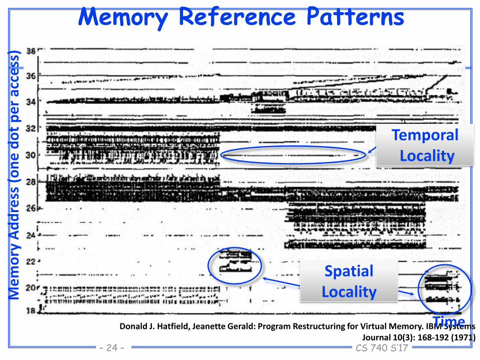
Two predictable properties ofmemory references:
Temporal Locality: If a location is referenced it is likely to be referenced again in the near future.
Spatial Locality: If a location is referenced it is likely that locations near it will be referenced in the near future.
CS 740 S’17– 24 –
Memory Reference Patterns
Donald J. Hatfield, Jeanette Gerald: Program Restructuring for Virtual Memory. IBM Systems Journal 10(3): 168-192 (1971)
Time
Me
mo
ry A
dd
ress
(o
ne
do
t p
er
acce
ss)
SpatialLocality
TemporalLocality

CS 740 S’17– 25 –
Memory Hierarchy
Implement memories of different sizes to serve different latency / latency / bandwidth tradeoffs
Keep frequently accessed data in small memories & large datasets in large memories
Provides illusion of a large & fast memory
Core
Big & FastMemory
Small, fast
Big, slow
CS 740 S’17– 26 –
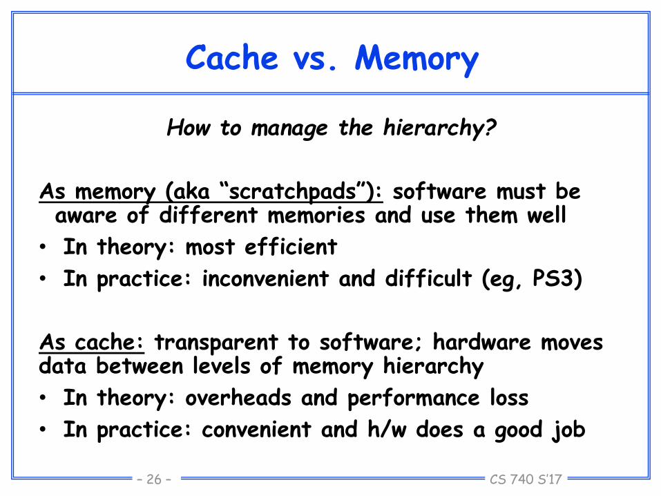
Cache vs. Memory
How to manage the hierarchy?
As memory (aka “scratchpads”): software must be aware of different memories and use them well
• In theory: most efficient
• In practice: inconvenient and difficult (eg, PS3)
As cache: transparent to software; hardware moves data between levels of memory hierarchy
• In theory: overheads and performance loss
• In practice: convenient and h/w does a good job
CS 740 S’17– 27 –
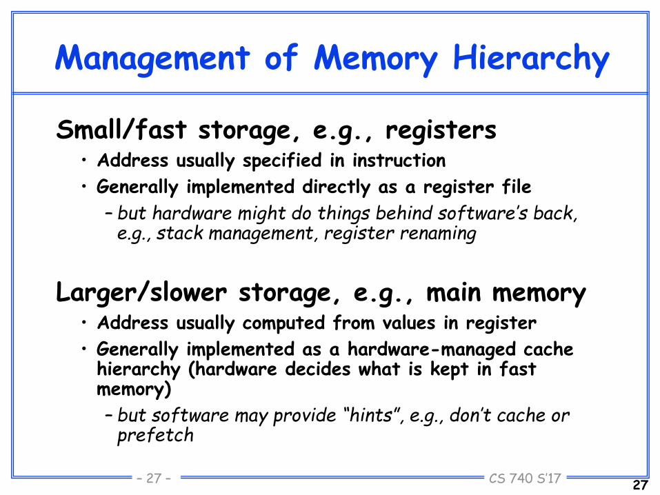
Management of Memory Hierarchy
Small/fast storage, e.g., registers• Address usually specified in instruction
• Generally implemented directly as a register file
– but hardware might do things behind software’s back, e.g., stack management, register renaming
Larger/slower storage, e.g., main memory• Address usually computed from values in register
• Generally implemented as a hardware-managed cache hierarchy (hardware decides what is kept in fast memory)
– but software may provide “hints”, e.g., don’t cache or prefetch
27

CS 740 S’17– 28 –
Alpha 21164 Chip Photo
Microprocessor Report 9/12/94
Caches:L1 data
L1 instruction
L2 unified
+ L3 off-chip
CS 740 S’17– 29 –
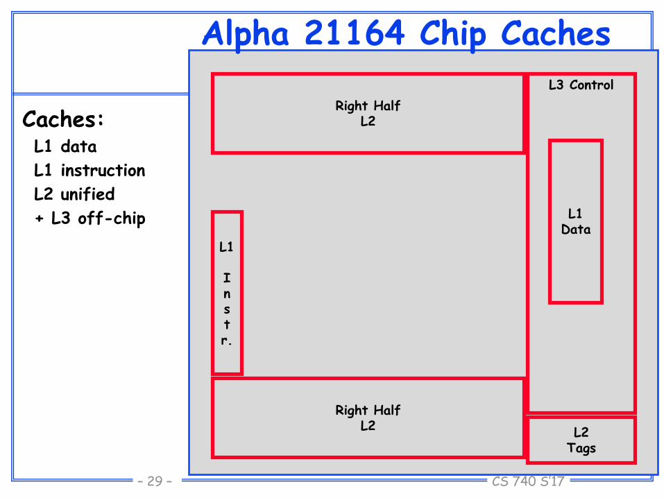
Alpha 21164 Chip Caches
Caches:L1 data
L1 instruction
L2 unified
+ L3 off-chip
Right HalfL2
Right HalfL2
L1
Instr.
L1Data
L2Tags
L3 Control

CS 740 S’17– 30 –
How important are caches?
(Figure from Jim Keller, Compaq Corp.)
•21264 Floorplan
•Register files in middle of execution units
•64k instr cache
•64k data cache
•Caches take up a large fraction of the die
• ~30-50% in recent chips

CS 740 S’17– 31 –
Multi-Level Caches
Memory disk
L1 Icache
L1 DcacheregsL2
Cache
Processor
Options: separate data and instruction caches, or a unified cache
How does this affect self modifying code?
CS 740 S’17– 32 –
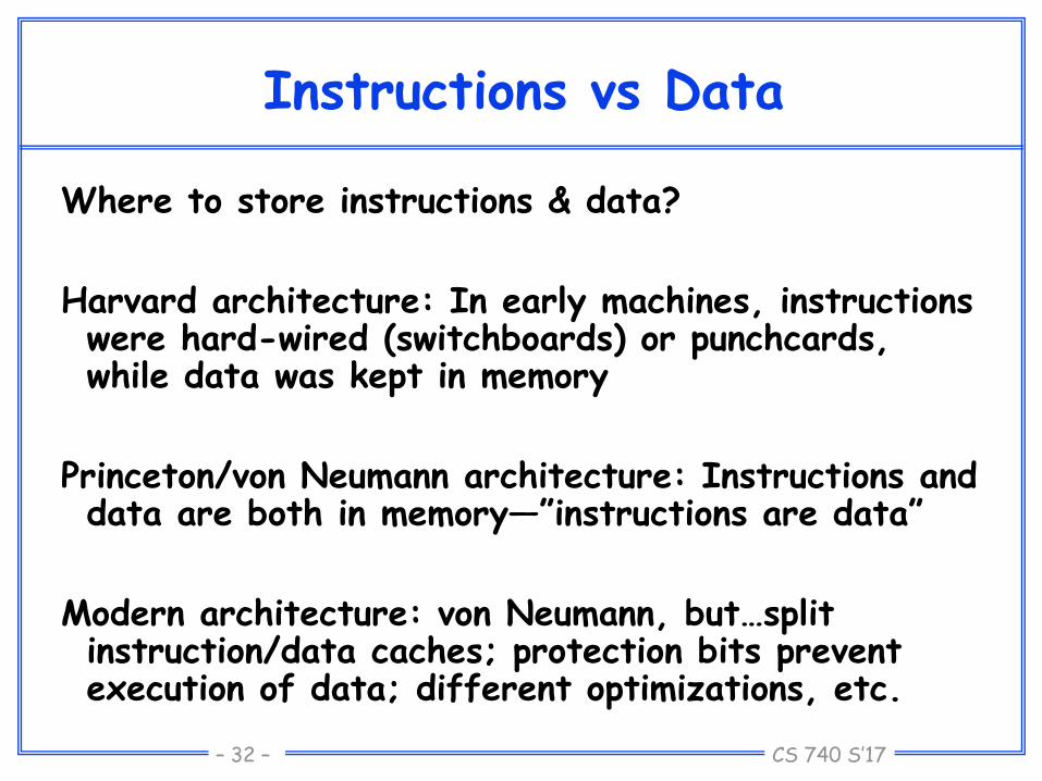
Instructions vs Data
Where to store instructions & data?
Harvard architecture: In early machines, instructions were hard-wired (switchboards) or punchcards, while data was kept in memory
Princeton/von Neumann architecture: Instructions and data are both in memory—”instructions are data”
Modern architecture: von Neumann, but…split instruction/data caches; protection bits prevent execution of data; different optimizations, etc.

CS 740 S’17– 33 –
Caches Exploit Locality
Temporal locality:
• Hardware decides what to keep in cache
• Replacement/eviction policy evicts a victim upon a cache miss
• Least-recently used (LRU) most common
Spatial locality:
• Cache stores multiple, neighboring words per block
• Prefetchers speculate about next accesses and fetch them into cache

CS 740 S’17– 34 –
Locality of Reference
Principle of Locality:• Programs tend to reuse data and instructions near those they
have used recently.
• Temporal locality: recently referenced items are likely to be referenced in the near future.
• Spatial locality: items with nearby addresses tend to be referenced close together in time.
sum = 0;
for (i = 0; i < n; i++)
sum += a[i];
*v = sum;Locality in Example:
• Data
– Reference array elements in succession (spatial)
– sum variable (temporal, allocated to register)
• Instructions
– Reference instructions in sequence (spatial)
– Cycle through loop repeatedly (temporal)

CS 740 S’17– 35 –
Caching: The Basic Idea
Main Memory• Stores words
A–Z in example
Cache• Stores subset of words
e.g., 4 in example
• Organized in lines
– Multiple words to…
– Exploit spatial locality
– Amortize overheads
Access• Processor requests address
from cache, which handles misses itself
Big, Slow Memory
A
B
C•
•
•
Y
Z
Small,
Fast Cache
A
B
G
H
Processor

CS 740 S’17– 36 –
Three ways to improve memory performance:
1. Reduce hit time
2. Reduce miss rate
3. Reduce miss penalty
There’s a tension between these
Memory Hierarchy Basics

CS 740 S’17– 37 –
Note that speculative and multithreaded processors may execute other instructions during a miss• Reduces performance impact of misses
• Memory-level parallelism (MLP) overlaps miss latency
Memory Hierarchy Basics

CS 740 S’17– 38 –
• Between any two levels, memory is divided into lines (aka “blocks”)
• Data moves between levels on demand, in line-sized chunks
• Invisible to application programmer
– Hardware responsible for cache operation
• Upper-level lines a subset of lower-level lines
a
ab
Access word w in line a (hit)
a
ab
Access word v in line b (miss)
w
b
a
b
ab
v
Accessing Data in Memory Hierarchy
L1
cache
L2
cache
CS 740 S’17– 39 –
Impact of Cache Size
Increasing cache size• Effect on cache area (tags + data)?
• Effect on hit time?
• Effect on miss rate?
• Effect on miss penalty?

CS 740 S’17– 40 –
Design Issues for Caches
Key Questions:• Where should a line be placed in the cache? (line placement)
• How is a line found in the cache? (line identification)
• Which line should be replaced on a miss? (line replacement)
• What happens on a write? (write strategy)
Constraints:• Design must be simple
– Hardware realization
– All decision making within nanosecond time scale
• Want to optimize performance for “typical” programs
– Do extensive benchmarking and simulations
– Many subtle engineering tradeoffs

CS 740 S’17– 41 –
Fully Associative Cache
Mapping of Memory Lines• Cache consists of single set holding A=S lines
• Given memory line can map to any line in set
• Only practical for small caches
• Useful for analysis and simulation
• Common in software caches
Entire Cache
0 1 • • • B–1Tag Valid
•
•
•
0 1 • • • B–1Tag Valid
0 1 • • • B–1Tag Valid
LRU State
Line 0:
Line 1:
Line A–1:
CS 740 S’17– 42 –
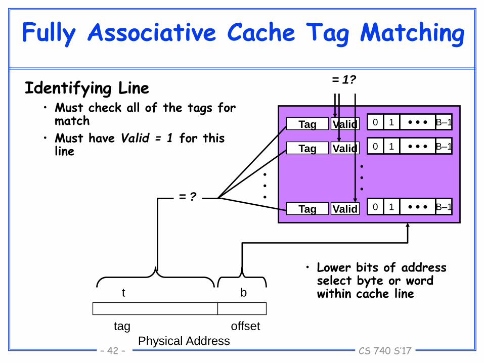
Fully Associative Cache Tag Matching
Identifying Line• Must check all of the tags for
match
• Must have Valid = 1 for this line
t b
tag offset
Physical Address
= ?
= 1?
• Lower bits of address select byte or word within cache line
0 1 • • • B–1Tag Valid
•
•
•
0 1 • • • B–1Tag Valid
0 1 • • • B–1Tag Valid
•
•
•

CS 740 S’17– 43 –
Direct-Mapped Caches
Simplest Design• Each memory line has a unique cache location
Parameters• Line (aka block) size B = 2b
– Number of bytes in each line– Typically 2X–8X word size
• Number of sets S = 2s
– Number of lines cache can hold• Total Cache Size = B*S = 2b+s
Physical Address• Address used to reference main memory• n bits to reference N = 2n total bytes• Partition into fields
– Offset: Lower b bits indicate which byte within line– Set: Next s bits indicate how to locate line within cache– Tag: Identifies this line when in cache
n-bit Physical Address
t s b
tag set index offset
CS 740 S’17– 44 –
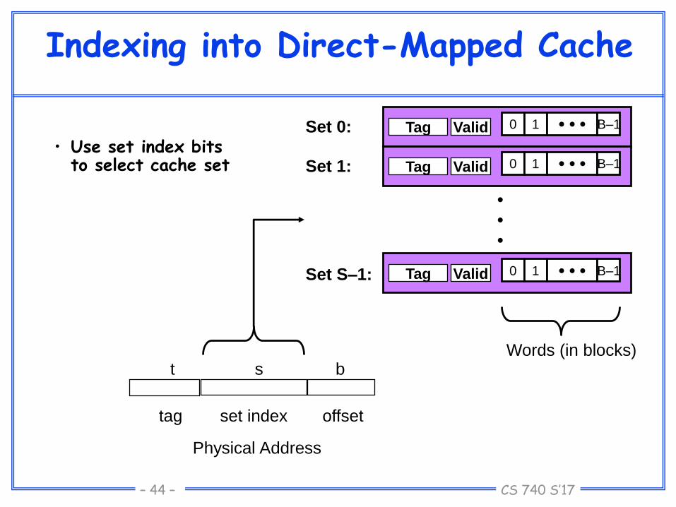
Indexing into Direct-Mapped Cache
• Use set index bits to select cache set
Set 0: 0 1 • • • B–1Tag Valid
0 1 • • • B–1Tag Valid
0 1 • • • B–1Tag Valid
Set 1:
Set S–1:
•
•
•
t s b
tag set index offset
Physical Address
Words (in blocks)

CS 740 S’17– 45 –
Direct-Mapped Cache Tag Matching
Identifying Line• Must have tag match high
order bits of address
• Must have Valid = 1
0 1 • • • B–1Tag Valid
Selected Set:
t s b
tag set index offset
Physical Address
= ?
= 1?
• Lower bits of address select byte or word within cache line
CS 740 S’17– 46 –
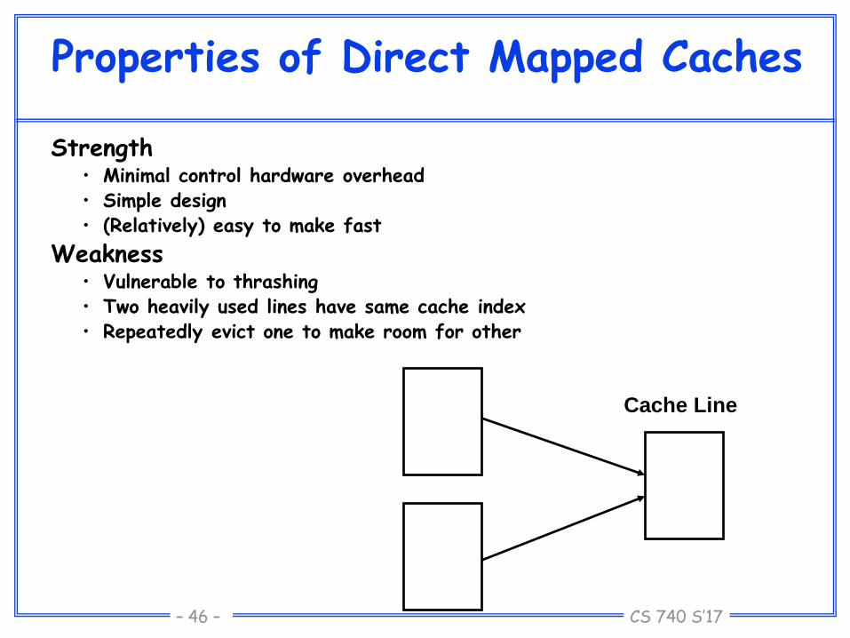
Properties of Direct Mapped Caches
Strength• Minimal control hardware overhead• Simple design• (Relatively) easy to make fast
Weakness• Vulnerable to thrashing• Two heavily used lines have same cache index• Repeatedly evict one to make room for other
Cache Line

CS 740 S’17– 47 –
Dot Product Example
Machine• DECStation 5000
• MIPS Processor with 64KB direct-mapped cache, 16 B line size
Performance• Good case: 24 cycles / element
• Bad case: 66 cycles / element
float dot_prod(float x[1024], y[1024])
{
float sum = 0.0;
int i;
for (i = 0; i < 1024; i++)
sum += x[i]*y[i];
return sum;
}
CS 740 S’17– 48 –
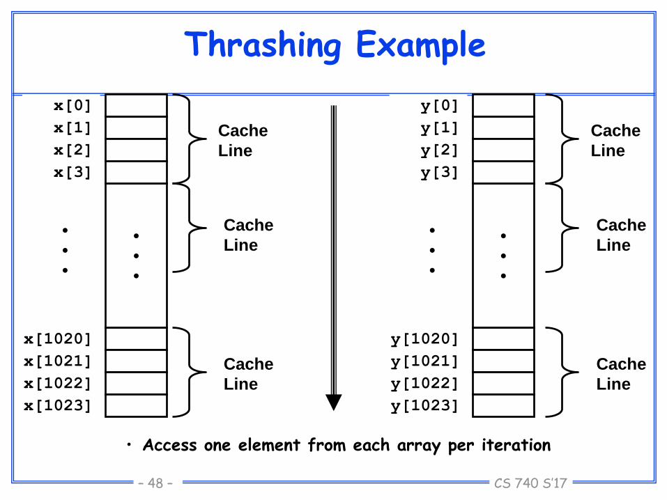
Thrashing Example
• Access one element from each array per iteration
x[1]
x[0]
x[1020]
•
•
•
•
•
•
x[3]
x[2]
x[1021]
x[1022]
x[1023]
y[1]
y[0]
y[1020]
•
•
•
•
•
•
y[3]
y[2]
y[1021]
y[1022]
y[1023]
Cache
Line
Cache
Line
Cache
Line
Cache
Line
Cache
Line
Cache
Line

CS 740 S’17– 49 –
x[1]
x[0]
x[3]
x[2]
y[1]
y[0]
y[3]
y[2]
Cache
Line
Thrashing Example: Good Case
Access Sequence• Read x[0]
– x[0], x[1], x[2], x[3] loaded• Read y[0]
– y[0], y[1], y[2], y[3] loaded• Read x[1]
– Hit• Read y[1]
– Hit• • • •• 2 misses / 8 reads
Analysis• x[i] and y[i] map to different cache
lines
• Miss rate = 25%
– Two memory accesses / iteration
– On every 4th iteration have two misses
Timing• 10 cycle loop time
• 28 cycles / cache miss
• Average time / iteration =
10 + 0.25 * 2 * 28
CS 740 S’17– 50 –
x[1]
x[0]
x[3]
x[2]
y[1]
y[0]
y[3]
y[2]
Cache
Line
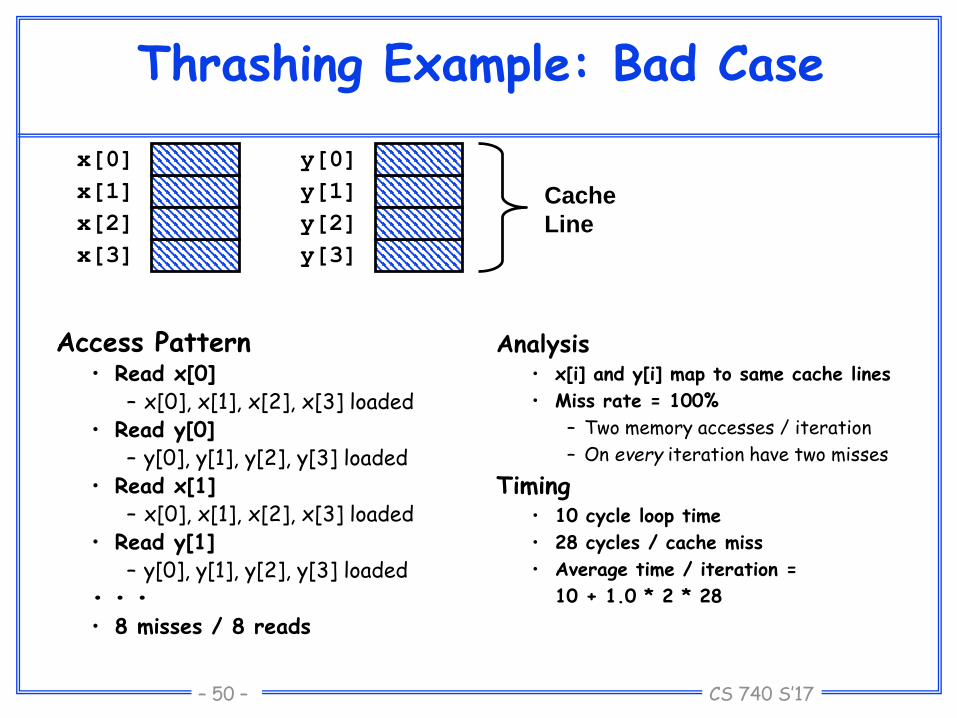
Thrashing Example: Bad Case
Access Pattern• Read x[0]
– x[0], x[1], x[2], x[3] loaded• Read y[0]
– y[0], y[1], y[2], y[3] loaded• Read x[1]
– x[0], x[1], x[2], x[3] loaded• Read y[1]
– y[0], y[1], y[2], y[3] loaded• • •• 8 misses / 8 reads
Analysis• x[i] and y[i] map to same cache lines
• Miss rate = 100%
– Two memory accesses / iteration
– On every iteration have two misses
Timing• 10 cycle loop time
• 28 cycles / cache miss
• Average time / iteration =
10 + 1.0 * 2 * 28
CS 740 S’17– 51 –
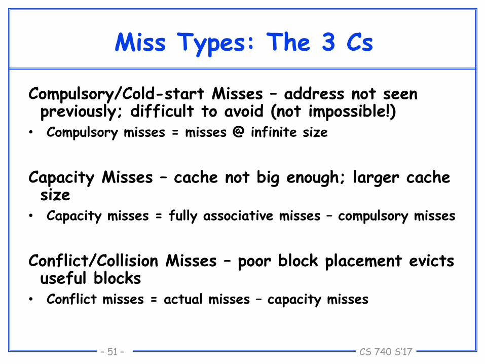
Miss Types: The 3 Cs
Compulsory/Cold-start Misses – address not seen previously; difficult to avoid (not impossible!)
• Compulsory misses = misses @ infinite size
Capacity Misses – cache not big enough; larger cache size
• Capacity misses = fully associative misses – compulsory misses
Conflict/Collision Misses – poor block placement evicts useful blocks
• Conflict misses = actual misses – capacity misses
CS 740 S’17– 52 –
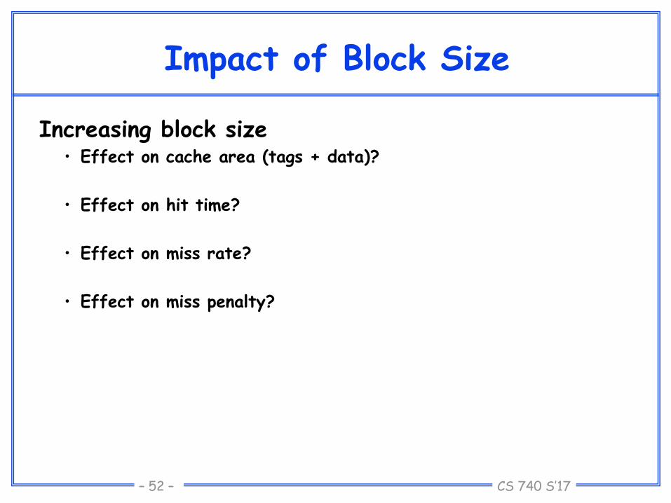
Impact of Block Size
Increasing block size• Effect on cache area (tags + data)?
• Effect on hit time?
• Effect on miss rate?
• Effect on miss penalty?
CS 740 S’17– 53 –
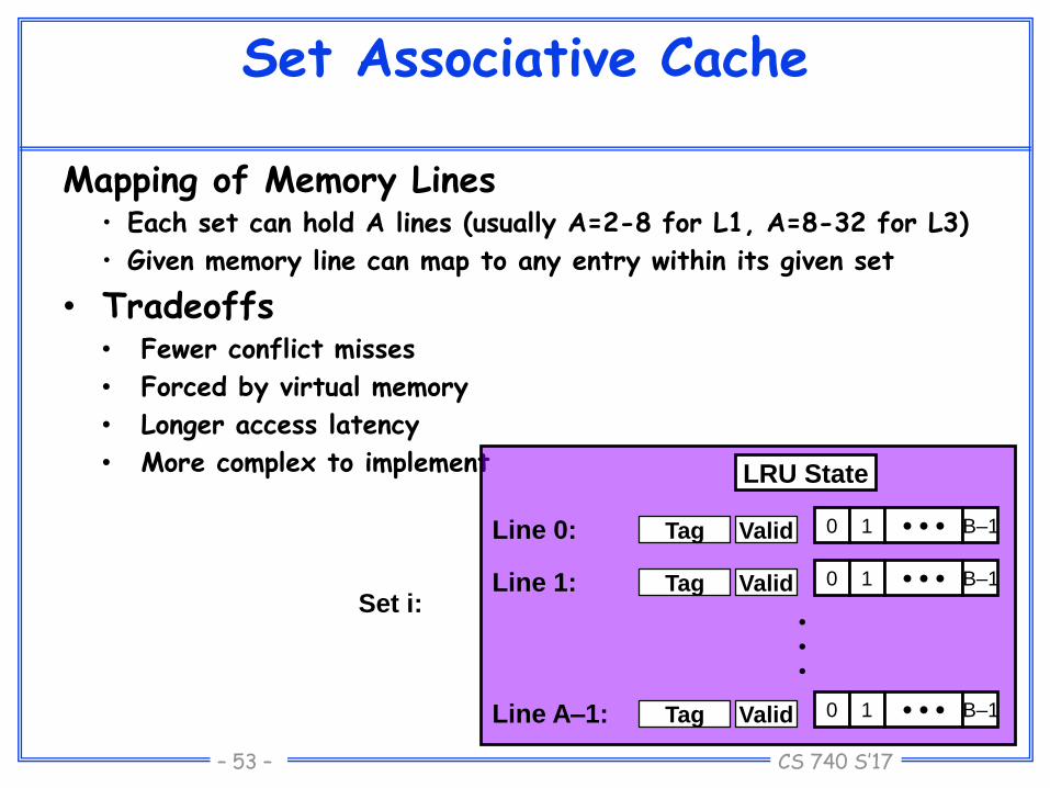
Set Associative Cache
Mapping of Memory Lines• Each set can hold A lines (usually A=2-8 for L1, A=8-32 for L3)
• Given memory line can map to any entry within its given set
• Tradeoffs• Fewer conflict misses
• Forced by virtual memory
• Longer access latency
• More complex to implement
Set i:
0 1 • • • B–1Tag Valid
•
•
•
0 1 • • • B–1Tag Valid
0 1 • • • B–1Tag Valid
LRU State
Line 0:
Line 1:
Line A–1:

CS 740 S’17– 54 –
Set 0:
Set 1:
Set S–1:
•
•
•
t s b
tag set index offset
Physical Address
Indexing into 2-Way Associative Cache
• Use middle s bits to select from among S = 2s
sets
0 1 • • • B–1Tag Valid
0 1 • • • B–1Tag Valid
0 1 • • • B–1Tag Valid
0 1 • • • B–1Tag Valid
0 1 • • • B–1Tag Valid
0 1 • • • B–1Tag Valid

CS 740 S’17– 55 –
Associative Cache Tag Matching
Identifying Line• Must have one of the
tags match high order bits of address
• Must have Valid = 1 for this line
Selected Set:
t s b
tag set index offset
Physical Address
= ?
= 1?
• Lower bits of address select byte or word within cache line
0 1 • • • B–1Tag Valid
0 1 • • • B–1Tag Valid
CS 740 S’17– 56 –
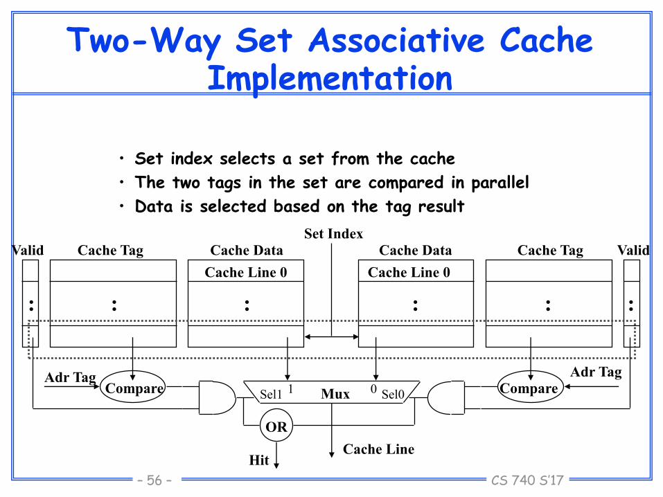
Two-Way Set Associative CacheImplementation
• Set index selects a set from the cache
• The two tags in the set are compared in parallel
• Data is selected based on the tag result
Cache Data
Cache Line 0
Cache TagValid
:: :
Cache Data
Cache Line 0
Cache Tag Valid
: ::
Set Index
Mux 01Sel1 Sel0
Cache Line
CompareAdr Tag
Compare
OR
Hit
Adr Tag

CS 740 S’17– 57 –
Impact of Associativity
Increasing associativity(eg, direct-mapped set associative fully associative)
Effect on cache area (tags+data)?
Hit time?
Miss rate?
Miss Penalty?

CS 740 S’17– 58 –
Replacement Algorithms
Optimal algorithm: (Belady/MIN/OPT)– replace the block that is next referenced furthest in the future
– but must know the future (can’t be implemented)
– tricky to prove optimality; only optimal under “vanilla” cache designs
Usage based algorithms:• Least-recently used (LRU)
– replace the block that has been referenced least recently
– hard to implement – but not really!
• Least-frequently used (LFU)
– replace the block that has been referenced the fewest times
– even harder to implement (“true” LFU—track blocks not in cache?)
• Many approximations: CLOCK, tree-based pseudo-LRU, etc
Non-usage based algorithms:• First-in First-out (FIFO)
– Weird pathologies (eg, hit rate degrades at larger cache size)
• Random (RAND)

CS 740 S’17– 59 –
Replacement Algorithms
Implementation
• FIFO: Keep per-set counter, replace block at counter offset + increment
• Random: Like FIFO, but a global counter instead
• Naïve LRU: encode ordering within set (n log n bits) + state machine
• Simple LRU: track time in # accesses, each candidate stores timestamp it was last accessed• Tradeoff?
• Efficiency vs complexity
• Coarsened ages (eg, high bits of timestamp) save space with ~no performance loss

CS 740 S’17– 60 –
Replacement Algorithms
Old & still active research area• Fix pathologies in, eg, LRU
• E.g.: ???
• Managing shared caches (“thread-aware” variants, cache partitioning)• Throughput vs fairness
• How to handle objects of different size?
• What observable factors correlate with reuse behavior?• Was referenced previously
• PC of referencing instruction
• Etc.
• What is best replacement metric if you don’t know the future?

CS 740 S’17– 61 –
Miss Types: The 3 Cs++
Compulsory misses - unchanged
Capacity Misses – cache not big enough• Capacity misses = fully associative misses with optimal
replacement – compulsory misses
Replacement misses: those due to sub-optimal replacement decisions
• Replacement misses = fully associative misses – capacity misses
Conflict/Collision Misses – poor block placement• Conflict misses = actual misses – replacement misses

CS 740 S’17– 62 –
Impact of Replacement Policy
Improving replacement policy(eg, random LRU)
Effect on cache area (tags+data)?
Hit time?
Miss rate?
Miss Penalty?

CS 740 S’17– 63 –
Write Policy
• What happens when processor writes to the cache?
• Should memory be updated as well?
Write Through:• Store by processor updates cache and memory
• Memory always consistent with cache
• Never need to store from cache to memory
• ~2X more loads than stores
Processor
Cache
Memory
Store
LoadCache
Load

CS 740 S’17– 64 –
Write Policy (Cont.)
Write Back:• Store by processor only updates cache line
• Modified line written to memory only when it is evicted
– Requires “dirty bit” for each line
»Set when line in cache is modified
»Indicates that line in memory is stale
• Memory not always consistent with cache
Processor
CacheMemory
Store
Load Cache
Load
Write
Back
CS 740 S’17– 65 –
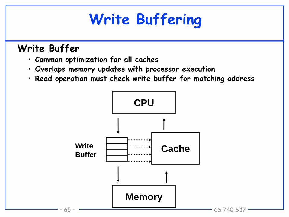
Write Buffering
Write Buffer• Common optimization for all caches• Overlaps memory updates with processor execution• Read operation must check write buffer for matching address
Cache
CPU
Memory
Write
Buffer
CS 740 S’17– 66 –
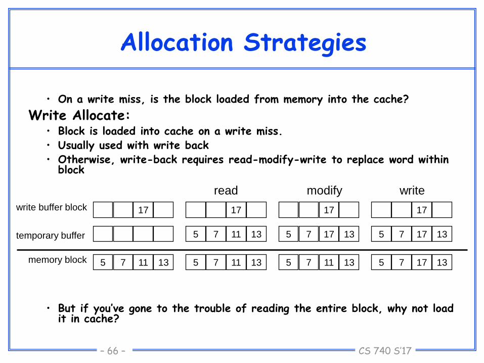
Allocation Strategies
• On a write miss, is the block loaded from memory into the cache?
Write Allocate: • Block is loaded into cache on a write miss.• Usually used with write back• Otherwise, write-back requires read-modify-write to replace word within
block
• But if you’ve gone to the trouble of reading the entire block, why not load it in cache?
17
5 7 11 13
write buffer block
memory block
17
5 7 11 13
read
5 7 11 13
17
5 7 11 13
modify
5 7 17 13
17
5 7 17 13
write
5 7 17 13temporary buffer
CS 740 S’17– 67 –
Allocation Strategies (Cont.)
• On a write miss, is the block loaded from memory into the cache?
No-Write Allocate (Write Around):• Block is not loaded into cache on a write miss
• Usually used with write through
– Memory system directly handles word-level writes

CS 740 S’17– 68 –
Impact of Write Policy
Writeback vs write-through
Effect on cache area (tags+data)?
Hit time?
Miss rate?
Miss Penalty?

CS 740 S’17– 69 –
EXAMPLE: MATRIX MULTIPLY
CS 740 S’17– 70 –
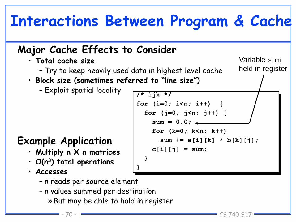
Interactions Between Program & Cache
Major Cache Effects to Consider• Total cache size
– Try to keep heavily used data in highest level cache• Block size (sometimes referred to “line size”)
– Exploit spatial locality
Example Application• Multiply n X n matrices• O(n3) total operations• Accesses
– n reads per source element– n values summed per destination
»But may be able to hold in register
/* ijk */
for (i=0; i<n; i++) {
for (j=0; j<n; j++) {
sum = 0.0;
for (k=0; k<n; k++)
sum += a[i][k] * b[k][j];
c[i][j] = sum;
}
}
Variable sum
held in register

CS 740 S’17– 71 –
0
20
40
60
80
100
120
140
160
25 50 75 100 125 150 175 200 225 250 275 300 325 350 375 400 425 450 475 500
matrix size (n)
mfl
op
s (d
.p.)
ijk
ikj
jik
jki
kij
kji
Matmult Performance (Alpha 21164)
Too big for L1 Cache Too big for L2 Cache

CS 740 S’17– 72 –
Block Matrix Multiplication
C11 = A11B11 + A12B21 C12 = A11B12 + A12B22
C21 = A21B11 + A22B21 C22 = A21B12 + A22B22
A11 A12
A21 A22
Example n=8, B = 4:
B11 B12
B21 B22X =
C11 C12
C21 C22
Key idea: Sub-blocks (i.e., Aij) can be treated just like scalars.

CS 740 S’17– 73 –
Blocked Matrix Multiply (bijk)
for (jj=0; jj<n; jj+=bsize) {
for (i=0; i<n; i++)
for (j=jj; j < min(jj+bsize,n); j++)
c[i][j] = 0.0;
for (kk=0; kk<n; kk+=bsize) {
for (i=0; i<n; i++) {
for (j=jj; j < min(jj+bsize,n); j++) {
sum = 0.0
for (k=kk; k < min(kk+bsize,n); k++) {
sum += a[i][k] * b[k][j];
}
c[i][j] += sum;
}
}
}
}

CS 740 S’17– 74 –
Blocked Matrix Multiply Analysis
A B C
block reused
n times
in succession
row sliver accessed
bsize times
Update successive
elements of sliver
i ikk
kk jjjj
for (i=0; i<n; i++) {
for (j=jj; j < min(jj+bsize,n); j++) {
sum = 0.0
for (k=kk; k < min(kk+bsize,n); k++) {
sum += a[i][k] * b[k][j];
}
c[i][j] += sum;
}
• Innermost loop pair multiplies 1 X bsize sliver of A times bsize X bsize block of B and accumulates into 1 X bsize sliver of C
• Loop over i steps through n row slivers of A & C, using same B
Innermost
Loop Pair

CS 740 S’17– 75 –
Blocked matmult perf (Alpha 21164)
0
20
40
60
80
100
120
140
160
50 75 100 125 150 175 200 225 250 275 300 325 350 375 400 425 450 475 500
matrix size (n)
mfl
op
s (
d.p
.)
bijk
bikj
ijk
ikj

CS 740 S’17– 76 –
ASSOCIATIVITYABSTRACTION

CS 740 S’17– 77 –
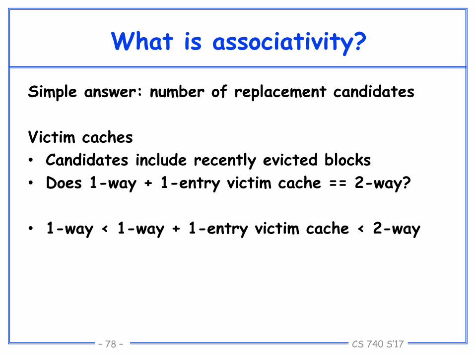
What is associativity?
Simple answer: number of replacement candidates
More associativity better hit rates
• 1-way < 2-way < 3-way < … < fully associative
CS 740 S’17– 78 –
What is associativity?
Simple answer: number of replacement candidates
Victim caches
• Candidates include recently evicted blocks
• Does 1-way + 1-entry victim cache == 2-way?
• 1-way < 1-way + 1-entry victim cache < 2-way

CS 740 S’17– 79 –
What is associativity?
Simple answer: number of replacement candidates
Hashing
• Hash address to compute set
• Reduce conflict misses
• Add latency + tag size + complexity
• 1-way < 1-way hashed < 2-way ??????
• 8-way < 8-way hashed ??????
CS 740 S’17– 80 –
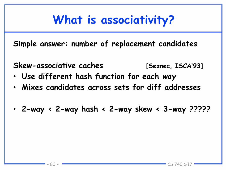
What is associativity?
Simple answer: number of replacement candidates
Skew-associative caches [Seznec, ISCA‘93]
• Use different hash function for each way
• Mixes candidates across sets for diff addresses
• 2-way < 2-way hash < 2-way skew < 3-way ?????

CS 740 S’17– 81 –
What is associativity?
Simple answer: number of replacement candidates
Associativity can be thought as a distribution of victims’ eviction priority [Sanchez, MICRO‘10]
• Distribution answers two questions: Among all cached blocks, how much did I want to evict the victim? (y-axis) How likely was that? (x-axis)
• Fully associative always evicts the highest rank
• Random sampling converges toward fully associative with larger samplers
• Can plot associativity distribution (eg, through simulation) for different cache organizations

CS 740 S’17– 82 –
Memory Hierarchy Summary
Gap between memory + compute is growing
Processors often spend most of their time + energy waiting for memory, not doing useful work
Hierarchy and locality are the key ideas to scale memory performance
Most systems use caches, which introduce many parameters to the design with many tradeoffs
• E.g., associativity—hit rate vs hit latency

CS 740 S’17– 83 –
Bandwidth Matching
Challenge• CPU works with short cycle times
• DRAM (relatively) long cycle times
• How can we provide enough bandwidth between processor & memory?
Effect of Caching• Caching greatly reduces amount of traffic to main
memory
• But, sometimes need to move large amounts of data from memory into cache
Trends• Need for high bandwidth much greater for multimedia
applications
– Repeated operations on image data
• Recent generation machines greatly improve on predecessors
CPU
cache
M
bus
Short
Latency
Long
Latency

CS 740 S’17– 84 –
High Bandwidth Memory Systems
CPU
cache
M
bus
mux
CPU
cache
M
bus
Solution 1
High BW DRAM
Solution 2
Wide path between memory & cache
Example:
Page Mode DRAM
RAMbus
Example: Alpha AXP 21064
256 bit wide bus, L2 cache,
and memory.

CS 740 S’17– 85 –
Cache Performance Metrics
Miss Rate• fraction of memory references not found in cache
(misses/references)• Typical numbers:
3-10% for L1can be quite small (e.g., < 1%) for L2, depending on size, etc.
Hit Time• time to deliver a line in the cache to the processor (includes time
to determine whether the line is in the cache)• Typical numbers:
1-3 clock cycles for L13-12 clock cycles for L2
Miss Penalty• additional time required because of a miss
– Typically 25-100 cycles for main memory

CS 740 S’17– 86 –
Qualitative Cache Performance Model
Miss Types• Compulsory (“Cold Start”) Misses• Capacity Misses• Replacement Misses
– Not universally included in classification• Conflict Misses• Coherence Misses
– Block invalidated by multiprocessor cache coherence mechanism
Hit Types• Reuse hit
– Accessing same word that previously accessed• Line hit
– Accessing word spatially near previously accessed word