the mn89305 is an lcd display controller ic ... - panasoniclsis for display 1 mn89305 xga lcd...
TRANSCRIPT

LSIs for Display
1
MN89305XGA LCD Display Controller
OverviewThe MN89305 is an LCD display controller IC that provides high-speed graphics and high-quality display. The
graphics accelerator supports 3-operand ROP operations and thus can draw Windows quickly. The MN89305 alsoprovides a full complement of power management functions to implement low-power video systems.
Features• LCD display functions
Color TFT (1024 × 768, 800 × 600, and 640 × 480)Color DSTN/SSTN (800 × 600 and 640 × 480)
• Display modes1024 × 768: 4 and 8 bpp800 × 600: 4, 8 and 16 bpp640 × 480: 4, 8 and 16 bpp
• Host interfacePCI v2.1 (33 MHz, 32 bits)ISA (16 bits), 386 and 486 (16 bits)
• Memory interface16M or 4M EDO × 16 × 1 (16-bit bus), × 2 (32-bit bus)
• Memory write FIFO32 bits × 4 stages or 16 stages
• Memory read cache32 bits × 4 stages
• BitBLT acceleratorVideo memory internal transfers (256 raster operations)Host to video memory transfers (256 raster operations)Pattern expansion (16 raster operations)Support for 3-operand raster operationsBit mapped data expansion and transferFilling of rectangular areas
• LCD panel screen size correctionThe screen size correction can be set independently in the horizontal and vertical directions.
• Power management mode• Automatic stop functions for clock supply to non-operation blocks (BitBLT and graphics blocks)
Standby modeSuspend modeSleep mode
• Supply voltage: 3.0 V to 3.6 V
Applications• Word processors, POS terminals and other equipment with LCD display
Note) 1. Windows is a registered trademark of Microsoft Corporation.
2. The term bpp stands for bits per pixel.
Mainten
ance/
Discon
tinued
Mainten
ance/D
iscont
inued
includ
es foll
owing
four P
roduct
lifecyc
le stag
e.
(planed
mainten
ance ty
pe, main
tenanc
e type,
planed
discon
tinued
typed,
discon
tinued
type)

MN89305 LSIs for Display
2
Block Diagram
MEMORY ACCESS ARBITRATOR
MEMORY I/F
EDO/Fast Page Mode DRAMs
PSCONVVIDEO FIFO
ATTBitBLTPATBLTSTRINGEXTEND
CRTC/LCDC
RAMGRAPHICS
GRAY SCALEENGINE
WRITEFIFO
READFIFO
HOST I/F
PCI/ISA/386/486
HALF FRAMECONTROL
LCD panel(TFT/SSTN/DSTN)
LCD I/F
PLL
SEQUENCER
Mainten
ance/
Discon
tinued
Mainten
ance/D
iscont
inued
includ
es foll
owing
four P
roduct
lifecyc
le stag
e.
(planed
mainten
ance ty
pe, main
tenanc
e type,
planed
discon
tinued
typed,
discon
tinued
type)

LSIs for Display MN89305
3
Function Block Descriptions1) Host interface
The host interface decodes the host bus addresses, generates the I/O and memory access enable signals, and transfersto the chip internal blocks required information for register read and write operations and for memory read and writeoperations. Data transfers are performed in 16-bit units for the ISA, 386, and 486 buses, and performed in 32-bit unitsfor the PCI bus.
Host bus type Data bus width
ISA 16 bits
386SX, 486, VL 16 bits
PCI 32 bits
Furthermore, since the MN89305 supports linear addressing, the CPU address calculation time can be reduced.Thus memory accesses are faster than if memory were accessed using a VGA compatible address area.
When the PCI interface is used, only burst transfers are supported for memory transfers. I/O bus transfers must notbe done. These burst transfers to memory can be performed only when addresses are incremented linearly.
Note) 1. ISA bus is a registered trademark of the (US) Industry Standards Architecture.
2. VL bus is a registered trademark of the (US) Video Electronics Standard Association.
3. PCI bus is a registered trademark of the (US) Peripheral Component Interconnect Association.
4. VGA is a registered trademark of International Business Machines, Inc.
2) Write FIFOThe write FIFO provides a function that temporarily accumulates memory write requests from the CPU bus, and
thus significantly increases the speed with which the LSI can handle CPU bus memory write requests. The FIFO canhold either 4 or 16 units of 32-bit data. This buffer compensates for the periods when the LSI cannot accept CPUmemory access requests, thus significantly reducing the wait time associated with CPU memory writes.
3) Read FIFO
When the LSI receives a memory read request from the CPU, the LSI loads data from consecutive memory addressesstarting at the address requests by the CPU into the read FIFO. This allows the LSI to quickly output data if the CPUissues memory read requests for consecutive addresses. If the CPU issues a request for data at an address not stored inthe FIFO, the data in the FIFO is all invalidated and then data from that new address is read out. The read FIFO can beused in graphics modes that use 256 or more colors.
4) Graphics controllerThe graphics controller processes data from the write FIFO according to the mode specified by the current register
settings. According to the operating mode, this module performs data expansion processing on the data from the writeFIFO and then the resultant data is sent to the memory access arbitrator. Furthermore, according to the operating mode,this module processes data read from memory and then sends the resultant data to the host interface.
5) Memory access arbitrator
The memory access arbitrator arbitrates memory access requests from the BitBLT block, display data read requestsfrom the LCD controller, and memory access requests from the half frame controller. It then sends the memory accessrequest, address, and data to the memory interface.
Mainten
ance/
Discon
tinued
Mainten
ance/D
iscont
inued
includ
es foll
owing
four P
roduct
lifecyc
le stag
e.
(planed
mainten
ance ty
pe, main
tenanc
e type,
planed
discon
tinued
typed,
discon
tinued
type)
MN89305 LSIs for Display
4
Block Functional Descriptions (continued)6) Memory access interface
The memory access interface accesses memory according to request signals from the memory access arbitrator.DRAM with fast page mode is used to write display data to memory as quickly as possible. The memory access interfacesupports variable memory access timings to get the maximum possible speed from memory when fast DRAMs are used.The memory access interface also outputs refresh signals according to the operating state of the chip.
7) CRT/LCD controllerThis block generates the display address, display enable, and vertical and horizontal synchronizing signals required
for display. It also performs image enlargement in the vertical direction.
8) Video FIFO/PSCONV
The video FIFO temporarily stores data read from memory by fast page mode, converts that data to dot unitsaccording to control signals from the CRT/LCD controller, and outputs that display data. In text mode, this circuitcalculates font addresses and issues access requests to the memory interface.
9) Attribute controllerThe attribute controller processes data from the video FIFO according to the display mode and generates color data
for each dot. It also implements blinking, underlining, and enlargement in the horizontal direction.
10) Color palette
The color palette generates 6-bit data for each of the three colors red, green, and blue by accessing internal palettememory according to data from the attribute controller.
11) Gray scale engineThe gray scale engine calculates a brightness level from a color signal and generates a monochrome level signal
when a monochrome STN LCD panel is used. This circuit supports two techniques for calculating the intensity: atechnique in which the G signal data is used directly as the intensity level and a technique in which the dot brightnessis calculated by simulating the NTSC luminance signal calculation. The generated monochrome level signal is outputas a gray-scale pattern optimal for that level. If a color STN is used, this circuit is used to generate gray-scale patternsfor each of the red, green, and blue data values from the color palette. These gray-scale patterns allow up to 32 levelsto be displayed by controlling the frame rate.
12) Half-frame controlWhen displaying on a DSTN panel, the post-level control data is stored for half the screen in video memory. Then,
a high refresh rate can be implemented at a low clock frequency by reading out data for half a frame from videomemory and sending that data to the LCD panel interface simultaneously with the data sent from the gray scale engine.
13) LCD panel interfaceThe LCD panel interface outputs the required synchronizing signals, data clock signals, and display data
appropriate for the type of LCD panel connected. This circuit supports both STN (including color and monochromeunits as well as SSTN and DSTN devices) and color TFT LCD panels. Note that if a DSTN panel is used, the data arealarge enough to hold a half frame of data must be allocated in video memory.
14) BitBLT engineThe BitBLT engine provides high-speed data transfers either from the host to video memory or between areas in
video memory. During these data transfers, the BitBLT engine supports 256 operations that correspond to three-operand (source, destination, and pattern) raster operations. These operations are supported only in the graphics displaymodes, and operate in packed pixel mode (8 or 16 bits per pixel).
Mainten
ance/
Discon
tinued
Mainten
ance/D
iscont
inued
includ
es foll
owing
four P
roduct
lifecyc
le stag
e.
(planed
mainten
ance ty
pe, main
tenanc
e type,
planed
discon
tinued
typed,
discon
tinued
type)
LSIs for Display MN89305
5
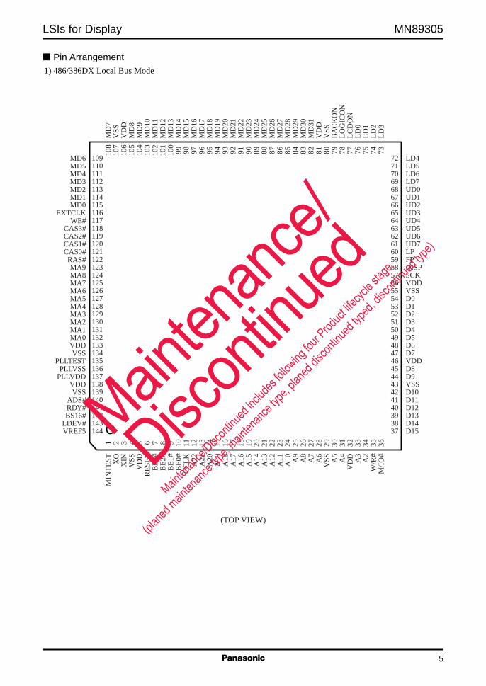
Pin Arrangement1) 486/386DX Local Bus Mode
MIN
TE
ST
1X
O2
XIN
3V
SS
4V
DD
5R
ES
ET
6B
E3#
7B
E2#
8B
E1#
9B
E0#
10C
CLK
11A
2212
A21
13A
2014
A19
15A
1816
A17
17A
1618
A15
19A
1420
A13
21A
1222
A11
23A
1024
A9
25A
826
A7
27A
628
VS
S29
A5
30A
431
VD
D32
A3
33A
234
W/R
#35
MD
710
7V
SS
106
VD
D10
5M
D8
104
MD
910
3M
D10
102
MD
1110
1M
D12
100
MD
1399
MD
1498
MD
1597
MD
1696
MD
1795
MD
1894
MD
1993
MD
2092
MD
2191
MD
2290
MD
2389
MD
2488
MD
2587
MD
2686
MD
2785
MD
2884
MD
2983
MD
3082
MD
3181
VD
D80
VS
S79
BA
CK
ON
78LO
GIC
ON
77LC
DO
N76
LD0
75LD
174
M/IO
#36
LD3
LD2
73
MD5MD4MD3MD2MD1MD0
EXTCLKWE#
CAS3#CAS2#CAS1#CAS0#RAS#MA9MA8MA7MA6MA5MA4MA3MA2MA1MA0VDDVSS
PLLTESTPLLVSS
PLLVDDVDDVSS
ADS#RDY#BS16#
LDEV#VREF5
LD571MD6 LD472
LD670LD769UD068UD167UD266UD365UD464UD563UD662UD761LP60FP59DISP58SCK57VDD56VSS55D054D153D252D351D450D549D648D747VDD46D845D944VSS43D1042D1141D1240D1339D1438D1537
110109
111112113114115116117118119120121122123124125126127128129130131132133134135136137138139140141142143144
108
(TOP VIEW)
Mainten
ance/
Discon
tinued
Mainten
ance/D
iscont
inued
includ
es foll
owing
four P
roduct
lifecyc
le stag
e.
(planed
mainten
ance ty
pe, main
tenanc
e type,
planed
discon
tinued
typed,
discon
tinued
type)

MN89305 LSIs for Display
6
Pin Arrangement (continued)2) 386SX Local Bus Mode
MIN
TE
ST
1X
O2
XIN
3V
SS
4V
DD
5R
ES
ET
6A
17
VS
S8
BE
H#
9B
EL#
10C
CLK
11A
2212
A21
13A
2014
A19
15A
1816
A17
17A
1618
A15
19A
1420
A13
21A
1222
A11
23A
1024
A9
25A
826
A7
27A
628
VS
S29
A5
30A
431
VD
D32
A3
33A
234
W/R
#35
MD
710
7V
SS
106
VD
D10
5M
D8
104
MD
910
3M
D10
102
MD
1110
1M
D12
100
MD
1399
MD
1498
MD
1597
MD
1696
MD
1795
MD
1894
MD
1993
MD
2092
MD
2191
MD
2290
MD
2389
MD
2488
MD
2587
MD
2686
MD
2785
MD
2884
MD
2983
MD
3082
MD
3181
VD
D80
VS
S79
BA
CK
ON
78LO
GIC
ON
77LC
DO
N76
LD0
75LD
174
M/IO
#36
LD3
LD2
73
MD5MD4MD3MD2MD1MD0
EXTCLKWE#
CAS3#CAS2#CAS1#CAS0#RAS#MA9MA8MA7MA6MA5MA4MA3MA2MA1MA0VDDVSS
PLLTESTPLLVSS
PLLVDDVDDVSS
ADS#RDY#BS16#
LDEV#VREF5
LD571MD6 LD472
LD670LD769UD068UD167UD266UD365UD464UD563UD662UD761LP60FP59DISP58SCK57VDD56VSS55D054D153D252D351D450D549D648D747VDD46D845D944VSS43D1042D1141D1240D1339D1438D1537
110109
111112113114115116117118119120121122123124125126127128129130131132133134135136137138139140141142143144
108
(TOP VIEW)
Mainten
ance/
Discon
tinued
Mainten
ance/D
iscont
inued
includ
es foll
owing
four P
roduct
lifecyc
le stag
e.
(planed
mainten
ance ty
pe, main
tenanc
e type,
planed
discon
tinued
typed,
discon
tinued
type)

LSIs for Display MN89305
7
Pin Arrangement (continued)3) ISA Bus Mode
MIN
TE
ST
1X
O2
XIN
3V
SS
4V
DD
5R
ES
ET
6M
EM
R#
7M
EM
W#
8IO
RD
#9
IOW
R#
10S
BH
E#
11A
EN
12A
2113
A20
14S
A19
15S
A18
16S
A17
17S
A16
18S
A15
19S
A14
20S
A13
21S
A12
22S
A11
23S
A10
24S
A9
25S
A8
26S
A7
27S
A6
28V
SS
29S
A5
30S
A4
31V
DD
32S
A3
33S
A2
34S
A1
35
MD
710
7V
SS
106
VD
D10
5M
D8
104
MD
910
3M
D10
102
MD
1110
1M
D12
100
MD
1399
MD
1498
MD
1597
MD
1696
MD
1795
MD
1894
MD
1993
MD
2092
MD
2191
MD
2290
MD
2389
MD
2488
MD
2587
MD
2686
MD
2785
MD
2884
MD
2983
MD
3082
MD
3181
VD
D80
VS
S79
BA
CK
ON
78LO
GIC
ON
77LC
DO
N76
LD0
75LD
174
SA
036
LD3
LD2
73
MD5MD4MD3MD2MD1MD0
EXTCLKWE#
CAS3#CAS2#CAS1#CAS0#RAS#MA9MA8MA7MA6MA5MA4MA3MA2MA1MA0VDDVSS
PLLTESTPLLVSS
PLLVDDVDDVSS
REFRESH#IOCHRDY#
IOCS16#MEMCS16#
VREF5
LD571MD6 LD472
LD670LD769UD068UD167UD266UD365UD464UD563UD662UD761LP60FP59DISP58SCK57VDD56VSS55SD054SD153SD252SD351SD450SD549SD648SD747VDD46SD845SD944VSS43SD1042SD1141SD1240SD1339SD1438SD1537
110109
111112113114115116117118119120121122123124125126127128129130131132133134135136137138139140141142143144
108
(TOP VIEW)
Mainten
ance/
Discon
tinued
Mainten
ance/D
iscont
inued
includ
es foll
owing
four P
roduct
lifecyc
le stag
e.
(planed
mainten
ance ty
pe, main
tenanc
e type,
planed
discon
tinued
typed,
discon
tinued
type)

MN89305 LSIs for Display
8
Pin Arrangement (continued)4) PCI Bus Mode
MIN
TE
ST
1X
O2
XIN
3V
SS
4V
DD
5R
ST
6C
/BE
3#7
C/B
E2#
8C
/BE
1#9
C/B
E0#
10C
LK11
FR
AM
E#
12ID
SE
L13
BIO
SC
S#
14T
ES
T2
15T
ES
T1
16T
ES
T0
17IR
DY
#18
AD
3119
AD
3020
AD
2921
AD
2822
AD
2723
AD
2624
AD
2525
AD
2426
AD
2327
AD
2228
VS
S29
AD
2130
AD
2031
VD
D32
AD
1933
AD
1834
AD
1735
MD
710
7V
SS
106
VD
D10
5M
D8
104
MD
910
3M
D10
102
MD
1110
1M
D12
100
MD
1399
MD
1498
MD
1597
MD
1696
MD
1795
MD
1894
MD
1993
MD
2092
MD
2191
MD
2290
MD
2389
MD
2488
MD
2587
MD
2686
MD
2785
MD
2884
MD
2983
MD
3082
MD
3181
VD
D80
VS
S79
BA
CK
ON
78LO
GIC
ON
77LC
DO
N76
LD0
75LD
174
AD
1636
LD3
LD2
73
MD5MD4MD3MD2MD1MD0
EXTCLKWE#
CAS3#CAS2#CAS1#CAS0#RAS#MA9MA8MA7MA6MA5MA4MA3MA2MA1MA0VDDVSS
PLLTESTPLLVSS
PLLVDDVDDVSSPAR
TRDY#STOP#
DEVSEL#VREF5
LD571MD6 LD472
LD670LD769UD068UD167UD266UD365UD464UD563UD662UD761LP60FP59DISP58SCK57VDD56VSS55AD054AD153AD252AD351AD450AD549AD648AD747VDD46AD845AD944VSS43AD1042AD1141AD1240AD1339AD1438AD1537
110109
111112113114115116117118119120121122123124125126127128129130131132133134135136137138139140141142143144
108
(TOP VIEW)
Mainten
ance/
Discon
tinued
Mainten
ance/D
iscont
inued
includ
es foll
owing
four P
roduct
lifecyc
le stag
e.
(planed
mainten
ance ty
pe, main
tenanc
e type,
planed
discon
tinued
typed,
discon
tinued
type)
LSIs for Display MN89305
9
Pin DescriptionsThis section describes the functions of each pin. The pins are classified by their I/O type as input (I), output (O),
or I/O (I/O). The Level column indicates the input interface levels for the pin, either 5 V TTL for 5 V inputs or CMOSfor 3.3 V CMOS inputs. Pin names that are followed by a number sign (#) are inverted logic (active low) signals.
1) 386/486 Local Bus Related Pins
Pin Name I/O Level Function
ADS# I 5 V TTL Address strobeIndicates that the host address is valid.
M/IO# I 5 V TTL Memory or I/O accessIndicates whether an access is a memory access or an I/O access. A high level
indicates a memory access and a low level indicates an I/O access.
W/R# I 5 V TTL Write/Read controlControls whether a host access is read or write. A high level indicates a write and
a low level indicates a read.
CCLK I 5 V TTL Local bus clockThe local bus clock
A[22 : 2] I 5 V TTL Host addressA1(386SX) These inputs are the host address bus.
BE[3 : 0]# I 5 V TTL Byte enable (486/386DX) These inputs indicate which bytes in the data bus are valid.
BEH# (386SX)
BEL# (386SX)
D[15 : 0] I/O 5 V TTL Data busHost data bus I/O signals.
RDY# I/O 5 V TTL ReadyIndicates to the host that processing has completed.
External circuits can monitor the external -RDY signal to determine when a 386
mode pipelined sequence has completed.
LDEV# O Local deviceIndicates to the host that this chip was accessed as a local bus device.
BS16# O 16-bit data busIndicates to the host that this chip was accessed as a 16-bit device.
2) ISA Bus Related Pins
Pin Name I/O Level Function
AEN I 5 V TTL Address enableA high level on this input indicates that a DMA operation is in progress. Therefore,
the MN89305 will not respond to an I/O access when this input is high.
Mainten
ance/
Discon
tinued
Mainten
ance/D
iscont
inued
includ
es foll
owing
four P
roduct
lifecyc
le stag
e.
(planed
mainten
ance ty
pe, main
tenanc
e type,
planed
discon
tinued
typed,
discon
tinued
type)
MN89305 LSIs for Display
10
Pin Descriptions (continued)2) ISA Bus Related Pins (continued)
Pin Name I/O Level Function
SBHE# I 5 V TTL System byte high enableIndicates how the 16-bit bus is being used.
SBHE SAO Bus status
0 0 16-bit transfer
0 1 High-order byte transfer
1 0 Low-order byte transfer
1 1 Disabled
IOWR# I 5 V TTL I/O writeIndicates an I/O write request.
IORD# I 5 V TTL I/O readIndicates an I/O read request.
MEMW# I 5 V TTL Memory writeIndicates a memory write request.
MEMR# I 5 V TTL Memory readIndicates a memory read request.
A[21 : 20] I 5 V TTL Address[21 : 20]Address bits 20 and 21.
SA[19 : 0] I 5 V TTL Address[19 : 0]Address bits 0 to 19
SD[15 : 0] I 5 V TTL Data[15 : 0]Host bus data bus pins
IOCHRDY# O I/O channel readyThis pin outputs either a low level or a high-impedance state. It goes to the low
level when a wait is applied to either an I/O or memory access.
MEMCS16# O Memory chip select 16This pin outputs either a low level or a high-impedance state. A low-level output
from this pin for a memory access to this chip informs the system that 16-bit
transfers are possible for this memory access. Note that 16-bit transfers are always
possible for accesses to display memory.
IOCS16# O I/O chip select 16This pin outputs either a low level or a high-impedance state. A low-level output
from this pin for an I/O access to this chip informs the system that 16-bit transfers
are possible for this I/O access.
REFRESH# I 5 V TTL RefreshA low level input to this pin indicates the timing for DRAM refresh. All memory
access requests issued when this input is low are ignored.
Mainten
ance/
Discon
tinued
Mainten
ance/D
iscont
inued
includ
es foll
owing
four P
roduct
lifecyc
le stag
e.
(planed
mainten
ance ty
pe, main
tenanc
e type,
planed
discon
tinued
typed,
discon
tinued
type)

LSIs for Display MN89305
11
Pin Descriptions (continued)3) PCI Bus Related Pins
Pin Name I/O Level Function
CLK I 5 V TTL PCI clockPCI bus synchronization clock. A clock frequency of up to 33 MHz can be used.
AD[31 : 0] I/O 5 V TTL Address data busTime-division multiplexed PCI address and data bus.
C/BE[3 : 0]# I 5 V TTL Command/Byte enableDuring the address phase, these lines indicate the command which can be a
memory access, an I/O access, a configuration access, or a read/write operation.
During the data phase, these lines function as byte enable signals.
PAR I/O 5 V TTL Bus parityEither the parity input or parity output at the read command.
FRAME# I 5 V TTL Cycle frameIndicates the period during which the data transfer is performed. The transfer
cycle starts when this input goes low, and the transfer completes at the next data
transfer when this input has become high.
IRDY# I 5 V TTL Initiator readyA single data phase completes on the cycle during which both IRDY# and TRDY#
are low.
TRDY# O Target readyA single data phase completes on the cycle during which both IRDY# and TRDY#
are low.
STOP# O StopThis signal is output when this IC stopped the currently executing data transfer
halfway.
IDSEL I 5 V TTL Initialization device selectChip select signal of the configuration register. The configuration register can be
accessed when this signal is high. If the AD signal is used as IDSEL, we
recommend connecting AD24 through AD31.
DEVSEL# O Device selectOutputs a low level when an access request to this IC is detected.
BIOSCS# O BIOS chip selectOutputs a low level when accepting an access to the video BIOS.
Mainten
ance/
Discon
tinued
Mainten
ance/D
iscont
inued
includ
es foll
owing
four P
roduct
lifecyc
le stag
e.
(planed
mainten
ance ty
pe, main
tenanc
e type,
planed
discon
tinued
typed,
discon
tinued
type)
MN89305 LSIs for Display
12
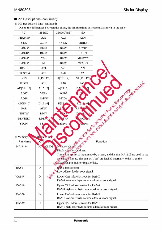
Pin Descriptions (continued)3) PCI Bus Related Pins (continued)
Due to the differences between the buses, the pin functions correspond as shown in the table.
PCI 386SX 386DX/486 ISA
FRAME# A22 A22 AEN
CLK CCLK CCLK SBHE#
C/BE0# BEL# BE0# IOWR#
C/BE1# BEH# BE1# IORD#
C/BE2# VSS BE2# MEMW#
C/BE3# A1 BE3# MEMR#
IDSEL A21 A21 A21
BIOSCS# A20 A20 A20
VSS A[19 : 17] A[19 : 17] SA[19 : 17]
IRDY# A16 A16 SA16
AD[31 : 18] A[15 : 2] A[15 : 2] SA[15 : 2]
AD17 W/R# W/R# SA1
AD16 M/IO# M/IO# SA0
AD[15 : 0] D[15 : 0] D[15 : 0] SD[15 : 0]
PAR ADS# ADS# REFRESH#
TRDY# RDY# RDY# IOCHRDY#
DEVSEL# LDEV# LDEV# MEMCS16#
STOP# BS16# BS16# IOCS16#
4) Memory Access Related Pins
Pin Name I/O Level Function
MA[9 : 0] I/O CMOS Memory addressDisplay memory address.
These pins are set to input mode by a reset, and the pins MA[2:0] are used to set
the chip host type. The pins MA[9:3] are latched internally to the IC as the
expansion pin monitor register data.
RAS# O RAS address strobeRow address latch strobe signal.
CAS0# O Lower CAS address strobe for RAM0RAM0 low-order byte column address strobe signal.
CAS1# O Upper CAS address strobe for RAM0RAM0 high-order byte column address strobe signal.
CAS2# O Lower CAS address strobe for RAM1RAM1 low-order byte column address strobe signal.
CAS3# O Upper CAS address strobe for RAM1RAM1 high-order byte column address strobe signal.
Mainten
ance/
Discon
tinued
Mainten
ance/D
iscont
inued
includ
es foll
owing
four P
roduct
lifecyc
le stag
e.
(planed
mainten
ance ty
pe, main
tenanc
e type,
planed
discon
tinued
typed,
discon
tinued
type)

LSIs for Display MN89305
13
Pin Descriptions (continued)4) Memory Access Related Pins (continued)
Pin Name I/O Level Function
WE# O Write enableData write signal
MD[31 : 0] I/O CMOS Memory data busThese lines are a 32-bit bus for DRAM, and can be switched to function as a 16-
bit bus by setting control register values.
This data bus is also used for video BIOS reads when a PCI bus connection is
used. In that case, the MD[15:0] lines are used as the BIOS ROM address and the
MD[23:16] lines are used as the BIOS ROM data inputs.
5) LCD Related Pins
Pin Name I/O Level Function
BACKON I/O CMOS Back light onOutputs a signal that requests that the backlight be turned on.
Low: Backlight off
High: Backlight on
This pin can also be used as a general-purpose I/O port.
In external RAMDAC mode, this pin is set to the output state and is used as the
register write signal to the RAMDAC.
LCDON I/O CMOS LCD drive power supply onOutputs a signal that requests that the LCD panel drive power supply be turned on.
Low: LCD drive power supply off
High: LCD drive power supply on
This pin can also be used as a general-purpose I/O port.
In external RAMDAC mode, this pin is set to the output state and is used as the
register address bit 0 signal to the RAMDAC.
LOGICON I/O CMOS LCD logic power supply onOutputs a signal that requests that the LCD panel logic system power supply be
turned on.
Low: LCD logic system power supply off
High: LCD logic system power supply on
This pin can also be used as a general-purpose I/O port.
In external RAMDAC mode, this pin is set to the output state and is used as the
register address bit 1 signal to the RAMDAC.
LP O Latch pulsePulse output that indicates the latch timing for one line of data for an STN LCD
panel. This output is used as the horizontal synchronizing signal when a TFT
LCD panel is used or in external RAMDAC mode.
FP O Frame pulsePulse output that indicates the frame start for an STN LCD panel. This output is
used as the vertical synchronizing signal when a TFT LCD panel is used or in
external RAMDAC mode.
Mainten
ance/
Discon
tinued
Mainten
ance/D
iscont
inued
includ
es foll
owing
four P
roduct
lifecyc
le stag
e.
(planed
mainten
ance ty
pe, main
tenanc
e type,
planed
discon
tinued
typed,
discon
tinued
type)

MN89305 LSIs for Display
14
Pin Descriptions (continued)5) LCD Related Pins (continued)
Pin Name I/O Level Function
DISP O Display enableDisplay enable signal output to the LCD. This output is used as the blanking
signal in external RAMDAC mode and as the display enable signal when a TFT
LCD panel is used.
SCK O Shift clockData shift clock output to an STN LCD panel. This output is used as the dot clock
output for a TFT LCD panel or in external RAMDAC mode.
UD[7 : 0] O Upper/Lower data 7 : 0
LD[7 : 0] Display data outputs.
In external RAMDAC mode LD[7:0] are used as the display data and UD[0:7] are
used as the write data lines to the RAMDAC register.
The table below shows the pin functions for each panel type.
Pin TFT STN(1S) STN(2S) External RAMDAC
DISP DEN DISP DISP BLANK
LP HSYNC LP LP HSYNC
FP VSYNC FP FP VSYNC
SCK DCLK SCK SCK DCLK
UD7 R4 UD7 WD7
UD6 R3 UD6 WD6
UD5 R2 UD5 WD5
UD4 R1 UD4 WD4
UD3 R0 UD3 WD3
UD2 G5 UD2 WD2
UD1 G4 UD1 WD1
UD0 G3 UD0 WD0
LD7 G2 LD7 LD7 P7
LD6 G1 LD6 LD6 P6
LD5 G0 LD5 LD5 P5
LD4 B4 LD4 LD4 P4
LD3 B3 LD3 LD3 P3
LD2 B2 LD2 LD2 P2
LD1 B1 LD1 LD1 P1
LD0 B0 LD0 LD0 P0
Note) 1. The pins marked with a dash () in the table are set to the output state, and therefore should be left open.
2. In external RAMDAC mode, WD[7:0] are used as write data to the external RAMDAC register.
Mainten
ance/
Discon
tinued
Mainten
ance/D
iscont
inued
includ
es foll
owing
four P
roduct
lifecyc
le stag
e.
(planed
mainten
ance ty
pe, main
tenanc
e type,
planed
discon
tinued
typed,
discon
tinued
type)
LSIs for Display MN89305
15
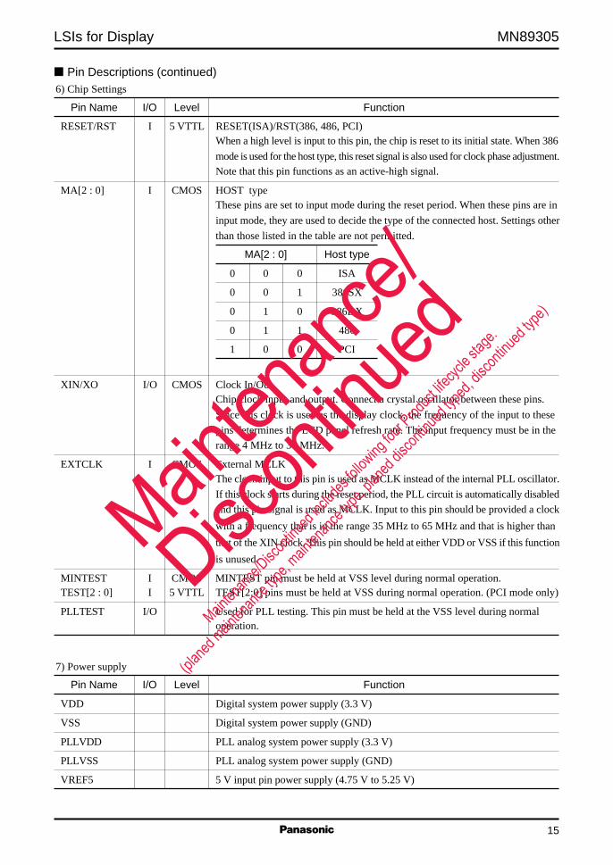
Pin Descriptions (continued)6) Chip Settings
Pin Name I/O Level Function
RESET/RST I 5 VTTL RESET(ISA)/RST(386, 486, PCI)When a high level is input to this pin, the chip is reset to its initial state. When 386
mode is used for the host type, this reset signal is also used for clock phase adjustment.
Note that this pin functions as an active-high signal.
MA[2 : 0] I CMOS HOST typeThese pins are set to input mode during the reset period. When these pins are in
input mode, they are used to decide the type of the connected host. Settings other
than those listed in the table are not permitted.
MA[2 : 0] Host type
0 0 0 ISA
0 0 1 386SX
0 1 0 386DX
0 1 1 486
1 0 0 PCI
XIN/XO I/O CMOS Clock In/OutChip clock input and output. Connect a crystal oscillator between these pins.
Since this clock is used as the display clock, the frequency of the input to these
pins determines the LCD panel refresh rate. The input frequency must be in the
range 4 MHz to 30 MHz.
EXTCLK I CMOS External MCLKThe clock input to this pin is used as MCLK instead of the internal PLL oscillator.
If this clock starts during the reset period, the PLL circuit is automatically disabled
and this pin signal is used as MCLK. Input to this pin should be provided a clock
with a frequency that is in the range 35 MHz to 65 MHz and that is higher than
that of the XIN clock. This pin should be held at either VDD or VSS if this function
is unused.
MINTEST I CMOS MINTEST pin must be held at VSS level during normal operation.TEST[2 : 0] I 5 VTTL TEST[2:0] pins must be held at VSS during normal operation. (PCI mode only)
PLLTEST I/O Used for PLL testing. This pin must be held at the VSS level during normaloperation.
7) Power supply
Pin Name I/O Level Function
VDD Digital system power supply (3.3 V)
VSS Digital system power supply (GND)
PLLVDD PLL analog system power supply (3.3 V)
PLLVSS PLL analog system power supply (GND)
VREF5 5 V input pin power supply (4.75 V to 5.25 V)
Mainten
ance/
Discon
tinued
Mainten
ance/D
iscont
inued
includ
es foll
owing
four P
roduct
lifecyc
le stag
e.
(planed
mainten
ance ty
pe, main
tenanc
e type,
planed
discon
tinued
typed,
discon
tinued
type)

MN89305 LSIs for Display
16
Electrical Characteristics1. Absolute Maximum Ratings at VSS = VSSPLL = 0 V
Parameter Symbol Rating Unit
Supply voltage VDD − 0.3 to +4.6 V
VDDPLL
5 V reference voltage †1 VREF5 − 0.3 to +5.7 V
Input pin voltage (except TYPE* ) VI − 0.3 to VDD+0.3 V
Input pin voltage (TYPE-A) VI5 − 0.3 to +6.0 †2 V
Input pin voltage (TYPE-B) VI − 0.3 to VDDPLL+0.3 V
Input pin voltage (TYPE-C) VI5 − 0.3 to VREF5+0.3 †2 V
Output pin voltage (except TYPE*) VO − 0.3 to VDD+0.3 V
Output pin voltage (TYPE-C) VO5 − 0.3 to VREF5+0.3 †2 V
Output current (TYPE-HL1) IO ±3 mA
Output current (TYPE-HL2) IO ±6 mA
Output current (TYPE-HL4) IO ±12 mA
Output current (TYPE-HL8) IO ±24 mA
Power dissipation PD 700 mW
Operating temperature Topr 0 to +70 °C
Storage temperature Tstg −55 to +150 °CNote) 1. †1:The power application sequence must meet the following stipulations.
The periods t3-5 and t5-3 must be 0 or longer.
VDD and VREF5 must change smoothly.
If the periods t3-5 and t5-3 ever become negative, VREF5 − VDD must be less than 3.6 V.
†2:When VDD ≤ 1.4 V: −0.3 V to +4.6 V.
2. Type A pins: A21, SA16 to SA19, AEN, IORD#, IOWR#, MEMR#, MEMW#, SBHE#, RESET
Type B pins: PLLTEST
Type C pins: A20, SA0 to SA15, SD0 to SD15, IOCS16#, MEMCS16#, IOCHRDY#, REFRESH#
Type HL1 pins: A20, MD0 to MD31, LCDON, BACKON, EXTCLK, LOGICON
Type HL2 pins: MA0 to MA9, SA0 to SA15, SD0 to SD15, WE#, CAS0# to CAS3#, RAS#
Type HL4 pins: FP, LD0 to LD7, LP, UD0 to UD7, SCK, DISP
Type HL8 pins: IOCS16#, MEMCS16#, IOCHRDY#, REFRESH#
3. The absolute maximum ratings are limiting values under which the chip will not be destroyed. Operation is not guaranteed
within these ranges.
4. All of the VDD, PLVDD, VSS, PLVSS, and VREF5 pins must connected directly, and by the shortest routes possible, to the
power supply or ground, respectively.
5. The crystal oscillator element used must be evaluated thoroughly in advance using the oscillator cell for this device.
6. Apply identical voltages to the VDD and PLVDD pins.
VDD 0 V
t3-5
VREF5 0 V
t5-3
Mainten
ance/
Discon
tinued
Mainten
ance/D
iscont
inued
includ
es foll
owing
four P
roduct
lifecyc
le stag
e.
(planed
mainten
ance ty
pe, main
tenanc
e type,
planed
discon
tinued
typed,
discon
tinued
type)

LSIs for Display MN89305
17
Parameter Symbol Conditions Min Typ Max Unit
Supply voltage VDD 3.0 3.3 3.6 VVDDPLL
5 V reference voltage VREF5 4.75 5.0 5.25 V
Ambient temperature Ta 0 70 °C
Input rise time tr 0 100 ns
Input fall time tf 0 100
Oscillator frequency fOSC 30 MHz Xtal 5 30 MHz
Recommended external CXIN VDD = 3.3 V 47 pF
capacitors CXO The feedback resistor is built in. 47
Electrical Characteristics (continued)2. Recommended Operating Conditions at VSS = VSSPLL = 0 V
XINCXIN
CXO
XO
Note) The oscillator characteristics differ depending on the device used, external capacitors, and other conditions. Consult with
the manufacturer of the oscillator element to determine appropriate circuit values.
Apply identical voltages to the VDD and PLVDD pins.
3. DC Characteristics at VDD = VDDPLL = 3.0 V to 3.6 V, VREF5 = 4.75 V to 5.25 V, VSS = VSSPLL = 0.00 V,
fTEST = 20 MHz, Ta = 0°C to 70°C
Parameter Symbol Conditions Min Typ Max Unit
Quiescent current IDDS VI (pull up) = OPEN 30 µAVI (pull down) = OPEN
VI (XIN) = VDD†
Apply either the VSS or VDD
level at the same time to
all other input pins and
I/O pins in the high-
impedance state.
VDD = VDDPLL = 3.6 V
VREF5 = 5.25 V
Ta = 25°C
5 V reference supply (VREF5) IREF5 VDD = VDDPLL = 3.6 V −20 20 µAinput leakage current VREF5 = 5.25 V
Operating supply current IDD0 VI = VDD or VSS 95 mAf = 20 MHz, output pins open
VDD = VDDPLL = 3.3 V
VREF5 = 5.0 V
Note) †: VDD applied to the XIN pin is another power supply than that used in IDDS measurement.
Mainten
ance/
Discon
tinued
Mainten
ance/D
iscont
inued
includ
es foll
owing
four P
roduct
lifecyc
le stag
e.
(planed
mainten
ance ty
pe, main
tenanc
e type,
planed
discon
tinued
typed,
discon
tinued
type)

MN89305 LSIs for Display
18
Electrical Characteristics (continued)3. DC Characteristics at VDD = VDDPLL = 3.0 V to 3.6 V, VREF5 = 4.75 V to 5.25 V, VSS = VSSPLL = 0.00 V,
fTEST = 20 MHz, Ta = 0°C to 70°C (continuted)
Parameter Symbol Conditions Min Typ Max Unit
Operating supply current IDD1 VI = VDD or VSS 35 mAStandby mode f = 20 MHz, output pins open
VDD = VDDPLL = 3.3 V
VREF5 = 5.0 V
With the IC set to standby
mode via register settings.
Operating supply current IDD2 VI = VDD or VSS 5 mASuspend mode f = 20 MHz, output pins open
VDD = VDDPLL = 3.3 V
VREF5 = 5.0 V
With the IC set to suspend
mode via register settings.
Operating supply current IDD3 VI = VDD or VSS 1 mASleep mode f = 0 MHz, output pins open
VDD = VDDPLL = 3.3 V
VREF5 = 5.0 V
With the IC set to sleep
mode via register settings.
Oscillator Circuit: XO
Internal feedback resistor Rf7 VI = VDD or VSS 313 940 2820 kΩVDD = 3.3 V
Oscillator Circuit Input: XIN
Input leakage current ILI With the XO oscillator stopped ±5 µAVI = VDD or VSS
VDD = 3.3 V
Input with pull-down resisitor (CMOS level): MINTEST
High-level input voltage VIH VDD × 0.7 VDD V
Low-level input voltage VIL 0 VDD × 0.3 V
Pull-down resistor RIL VI = VDD = 3.3 V 10 30 90 kΩ
Input leakage current ILIL VI = VSS ±10 µA
Input (TTL level): A21, SA16 to SA19, AEN, IORD#, IOWR#, MEMR#, MEMW#, SBHE#
High-level input voltage VIH 2.0 5.25 V
Low-level input voltage VIL 0 0.8 V
Input leakage current ILI VI = 5.25 V or VSS ±10 µA
Mainten
ance/
Discon
tinued
Mainten
ance/D
iscont
inued
includ
es foll
owing
four P
roduct
lifecyc
le stag
e.
(planed
mainten
ance ty
pe, main
tenanc
e type,
planed
discon
tinued
typed,
discon
tinued
type)
LSIs for Display MN89305
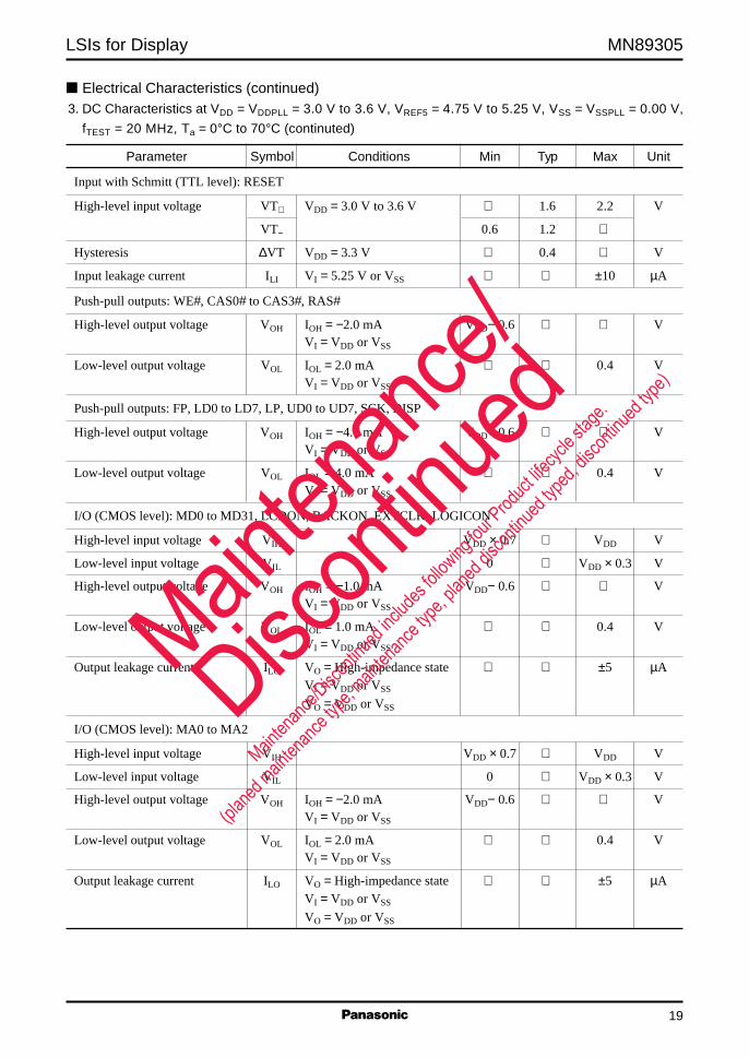
19
Electrical Characteristics (continued)3. DC Characteristics at VDD = VDDPLL = 3.0 V to 3.6 V, VREF5 = 4.75 V to 5.25 V, VSS = VSSPLL = 0.00 V,
fTEST = 20 MHz, Ta = 0°C to 70°C (continuted)
Parameter Symbol Conditions Min Typ Max Unit
Input with Schmitt (TTL level): RESET
High-level input voltage VT+ VDD = 3.0 V to 3.6 V 1.6 2.2 V
VT− 0.6 1.2
Hysteresis ∆VT VDD = 3.3 V 0.4 V
Input leakage current ILI VI = 5.25 V or VSS ±10 µA
Push-pull outputs: WE#, CAS0# to CAS3#, RAS#
High-level output voltage VOH IOH = −2.0 mA VDD− 0.6 VVI = VDD or VSS
Low-level output voltage VOL IOL = 2.0 mA 0.4 VVI = VDD or VSS
Push-pull outputs: FP, LD0 to LD7, LP, UD0 to UD7, SCK, DISP
High-level output voltage VOH IOH = −4.0 mA VDD− 0.6 VVI = VDD or VSS
Low-level output voltage VOL IOL = 4.0 mA 0.4 VVI = VDD or VSS
I/O (CMOS level): MD0 to MD31, LCDON, BACKON, EXTCLK, LOGICON
High-level input voltage VIH VDD × 0.7 VDD V
Low-level input voltage VIL 0 VDD × 0.3 V
High-level output voltage VOH IOH = −1.0 mA VDD− 0.6 VVI = VDD or VSS
Low-level output voltage VOL IOL = 1.0 mA 0.4 VVI = VDD or VSS
Output leakage current ILO VO = High-impedance state ±5 µAVI = VDD or VSS
VO = VDD or VSS
I/O (CMOS level): MA0 to MA2
High-level input voltage VIH VDD × 0.7 VDD V
Low-level input voltage VIL 0 VDD × 0.3 V
High-level output voltage VOH IOH = −2.0 mA VDD− 0.6 VVI = VDD or VSS
Low-level output voltage VOL IOL = 2.0 mA 0.4 VVI = VDD or VSS
Output leakage current ILO VO = High-impedance state ±5 µAVI = VDD or VSS
VO = VDD or VSS
Mainten
ance/
Discon
tinued
Mainten
ance/D
iscont
inued
includ
es foll
owing
four P
roduct
lifecyc
le stag
e.
(planed
mainten
ance ty
pe, main
tenanc
e type,
planed
discon
tinued
typed,
discon
tinued
type)
MN89305 LSIs for Display
20
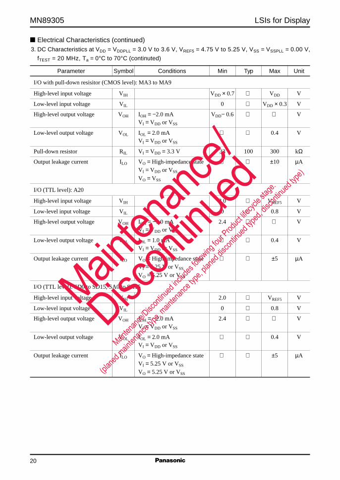
Electrical Characteristics (continued)3. DC Characteristics at VDD = VDDPLL = 3.0 V to 3.6 V, VREF5 = 4.75 V to 5.25 V, VSS = VSSPLL = 0.00 V,
fTEST = 20 MHz, Ta = 0°C to 70°C (continuted)
Parameter Symbol Conditions Min Typ Max Unit
I/O with pull-down resisitor (CMOS level): MA3 to MA9
High-level input voltage VIH VDD × 0.7 VDD V
Low-level input voltage VIL 0 VDD × 0.3 V
High-level output voltage VOH IOH = −2.0 mA VDD− 0.6 VVI = VDD or VSS
Low-level output voltage VOL IOL = 2.0 mA 0.4 VVI = VDD or VSS
Pull-down resistor RIL VI = VDD = 3.3 V 33 100 300 kΩ
Output leakage current ILO VO = High-impedance state ±10 µAVI = VDD or VSS
VO = VSS
I/O (TTL level): A20
High-level input voltage VIH 2.0 VREF5 V
Low-level input voltage VIL 0 0.8 V
High-level output voltage VOH IOH = −1.0 mA 2.4 VVI = VDD or VSS
Low-level output voltage VOL IOL = 1.0 mA 0.4 VVI = VDD or VSS
Output leakage current ILO VO = High-impedance state ±5 µAVI = 5.25 V or VSS
VO = 5.25 V or VSS
I/O (TTL level): SD0 to SD15, SA0 to SA15
High-level input voltage VIH 2.0 VREF5 V
Low-level input voltage VIL 0 0.8 V
High-level output voltage VOH IOH = −2.0 mA 2.4 VVI = VDD or VSS
Low-level output voltage VOL IOL = 2.0 mA 0.4 VVI = VDD or VSS
Output leakage current ILO VO = High-impedance state ±5 µAVI = 5.25 V or VSS
VO = 5.25 V or VSS
Mainten
ance/
Discon
tinued
Mainten
ance/D
iscont
inued
includ
es foll
owing
four P
roduct
lifecyc
le stag
e.
(planed
mainten
ance ty
pe, main
tenanc
e type,
planed
discon
tinued
typed,
discon
tinued
type)

LSIs for Display MN89305
21
Electrical Characteristics (continued)3. DC Characteristics at VDD = VDDPLL = 3.0 V to 3.6 V, VREF5 = 4.75 V to 5.25 V, VSS = VSSPLL = 0.00 V,
fTEST = 20 MHz, Ta = 0°C to 70°C (continuted)
Parameter Symbol Conditions Min Typ Max Unit
I/O (TTL level): IOCS16#, MEMCS16#, IOCHRDY#, REFRESH#
High-level input voltage VIH 2.0 VREF5 V
Low-level input voltage VIL 0 0.8 V
High-level output voltage VOH IOH = −8.0 mA 2.4 VVI = VDD or VSS
Low-level output voltage VOL IOL = 8.0 mA 0.4 VVI = VDD or VSS
Output leakage current ILO VO = High-impedance state ±5 µAVI = 5.25 V or VSS
VO = 5.25 V or VSS
4. AC Characteristics (continued)
1) RESET Signal Timing (Applies to both the ISA and local bus)
No. Descriptions Min Max Unit
1 RESET high-level period 6 XIN
2 RESET setup time 5 ns
3 RESET hold time 8 ns
4 MA input switching time 4XIN+15 ns
5 MA output switching time 4XIN+15 ns
6 MA valid data input setup time 0 ns
7 MA valid data input hold time 3XIN+12 ns
RESET
XIN
MA Output OutputInput Valid data
1
2
45
76
3
Mainten
ance/
Discon
tinued
Mainten
ance/D
iscont
inued
includ
es foll
owing
four P
roduct
lifecyc
le stag
e.
(planed
mainten
ance ty
pe, main
tenanc
e type,
planed
discon
tinued
typed,
discon
tinued
type)

MN89305 LSIs for Display
22
Electrical Characteristics (continued)4. AC Characteristics (continued)
2) XIN Timing
No. Descriptions Min Max Unit
1 XIN rise time (external clock signal mode) 4 ns
2 XIN fall time (external clock signal mode) 4 ns
3 XIN high-level period (external clock signal mode) 14 ns
4 XIN low-level period (external clock signal mode) 14 ns
5 XIN period 30 ns
XIN
5
3 4
1 2
Note) The XIN clock determines the memory control timing and the LCD control timing.
Determine the XIN clock period based on the specifications of the DRAM and LCD panel used.
3) ISA Timing
AEN
REFRESH#
A[21 : 20]SA[19 : 0]SBHE#
IOCHRDY#
MEMCS16#
SD[15 : 0]
IORD#, IOWR#,MEMR#, MEMW#
1
3
5
7 8
6
4
12
1411
16
9 10Hi-ZHi-Z
Hi-ZHi-Z
13
2
15
IOCS16#18 Hi-ZHi-Z 17
No. Descriptions Min Max Unit
1 AEN setup time 20 ns
2 AEN hold time 10 ns
3 REFRESH# setup time 20 ns
4 REFRESH# hold time 10 ns
Mainten
ance/
Discon
tinued
Mainten
ance/D
iscont
inued
includ
es foll
owing
four P
roduct
lifecyc
le stag
e.
(planed
mainten
ance ty
pe, main
tenanc
e type,
planed
discon
tinued
typed,
discon
tinued
type)

LSIs for Display MN89305
23
No. Descriptions Min Max Unit
5 A[21:20], SA[19:0], and SBHE# setup time 20 ns
6 A[21:20], SA[19:0], and SBHE# hold time 10 ns
7 IOWR#, IORD#, MEMW#, and MEMR# low-level period 2MCLK+10 ns
8 IOWR#, IORD#, MEMW#, and MEMR# command inactive time 4MCLK+10 ns†2
9 IOWR#, IORD#, MEMW#, and MEMR# low to IOCHRDY# delay time 25 ns
10 IOCHRDY# low-level period 0 †1 ns
11 SD[15:0] setup time when IOWR# and MEMW# are active 20 ns
12 SD[15:0] hold time when IOWR# and MEMW# are active 10 ns
13 SD[15:0] delay time after IOCHRDY# goes to the high-impedance state 0 ns
when IOWR# and MEMW# are active
14 SD[15:0] hold time when IOWR# and MEMW# are active 2 30 ns
15 MEMCS16# active delay time after A[21:20] and SA[19:16] 25 ns
16 MEMCS16# inactive delay time after A[21:20] and SA[19:16] 25 ns
17 IOCS16# active delay time after SA[15:0] 25 ns
18 IOCS16# inactive delay time after SA[15:0] 25 ns
Electrical Characteristics (continued)4. AC Characteristics (continued)
3) ISA Timing (continued)
Note) 1. †1:Differs depending on the operating mode.
†2:7 MCLK inactive periods are required for MEMW# and MEMR# after word writes to GR06, SR08, SR0D, and
SR15.
7 MCLK inactive periods are required for IOWR# and IORD# after word writes to CR1A.
20 MCLK inactive periods are required for MEMW# and MEMR# after word writes to SR07.
2. MCLK in the table refers to one clock period of the memory clock.
3. Values listed in the table apply when the external load capacitor is 50 pF. The output delay times will differ depending on
the external load capacitor.
4) CCLK Timing (local bus)
CCLK
3
1 2
No. Descriptions Min Max Unit
1 CCLK rise time 4 ns
2 CCLK fall time 4 ns
3 CCLK period (486 mode) 30 †1 †1 ns
3 CCLK period (386 mode) 15 †2 †2 ns
Note) 1. †1:CCLK must meet the following condition: (MCLK + 5) < CCLK < (4 × MCLK) − 5
†2:CCLK must meet the following condition: (MCLK/2) + 5 < CCLK < (MCLK × 2) − 5
2. MCLK refers to one clock period of the memory clock.
Mainten
ance/
Discon
tinued
Mainten
ance/D
iscont
inued
includ
es foll
owing
four P
roduct
lifecyc
le stag
e.
(planed
mainten
ance ty
pe, main
tenanc
e type,
planed
discon
tinued
typed,
discon
tinued
type)
MN89305 LSIs for Display
24
Electrical Characteristics (continued)4. AC Characteristics (continued)
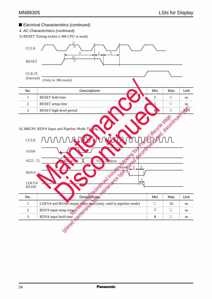
5) RESET Timing (when a 386 CPU is used)
No. Descriptions Min Max Unit
1 RESET hold time 2 ns
2 RESET setup time 5 ns
3 RESET high-level period 8 XIN
6) 386CPU RDY# Input and Pipeline Mode Timing
No. Descriptions Min Max Unit
1 LDEV# and BS16# output delay time (only valid in pipeline mode) 26 ns
2 RDY# input setup time 7 ns
3 RDY# input hold time 4 ns
CCLK
RESET
CLK1X(Internal) (Only in 386 mode)
3 1 2
CCLK
ADS#
A[23 : 2]
RDY#
LDEV#BS16#
Non VGA VGA Address
2 3
1
Input
Mainten
ance/
Discon
tinued
Mainten
ance/D
iscont
inued
includ
es foll
owing
four P
roduct
lifecyc
le stag
e.
(planed
mainten
ance ty
pe, main
tenanc
e type,
planed
discon
tinued
typed,
discon
tinued
type)

LSIs for Display MN89305
25
No. Descriptions Min Max Unit
1 A[23:2], M/IO#, BE[3:0]#, and W/R# setup time 15 ns
2 A[23:2], M/IO#, BE[3:0]#, and W/R# hold time 0 ns
3 ADS# setup time 15 ns
4 ADS# hold time 3 ns
5 BS16# active delay time 26 ns
6 BS16# inactive delay time 26 ns
7 BS16# high-level output time 15 ns
8 CPU write data setup time 6 ns
9 CPU write data hold time 0 ns
10 CPU read data setup time 2CLK−40 ns
11 CPU read data output off delay time 2 21 ns
12 RDY# setup time 1CLK−23 ns
13 RDY# hold time 2 ns
14 RDY# high-level output time 0.5CLK ns
15 CPU write wait time 1CLK † ns
16 CPU read wait time 2CLK † ns
17 LDEV# active delay time 26 ns
18 LDEV# inactive delay time 26 ns
Electrical Characteristics (continued)4. AC Characteristics (continued)
7) 486CPU Local Bus Timing
CCLK
LDEV#
D[15 : 0]
RDY#
W/R#
ADS#
BS16#
CPU WRITE CPU READ
A[23 : 2]M/IO#BE[3 : 0]#
1 2
1
9 10 118
12 13 1615
5
17 18
Hi-Z Hi-Z
6
3 4
2
7
14
Note) 1. †: The wait time differs depending on the chip status.
2. CLK in the table refers to one clock period of CCLK.
3. Values listed in the table apply when the external load capacitor is 50 pF. The output delay times will differ depending on
the external load capacitor.
Mainten
ance/
Discon
tinued
Mainten
ance/D
iscont
inued
includ
es foll
owing
four P
roduct
lifecyc
le stag
e.
(planed
mainten
ance ty
pe, main
tenanc
e type,
planed
discon
tinued
typed,
discon
tinued
type)

MN89305 LSIs for Display
26
No. Descriptions Min Max Unit
1 A[23:2], M/IO#, BE[3:0]#, and W/R# setup time 15 ns
2 A[23:2], M/IO#, BE[3:0]#, and W/R# hold time 0 ns
3 ADS# setup time 15 ns
4 ADS# hold time 3 ns
5 BS16# active delay time 26 ns
6 BS16# inactive delay time 26 ns
7 BS16# high-level output time 15 ns
8 CPU write data setup time 6 ns
9 CPU write data hold time 0 ns
10 CPU read data setup time 4CLK−40 ns
11 CPU read data output off delay time 2 21 ns
12 RDY# setup time 2CLK−23 ns
13 RDY# hold time 2 ns
14 RDY# high-level output time CLK ns
15 CPU write wait time 2CLK † ns
16 CPU read wait time 4CLK † ns
17 LDEV# active delay time 26 ns
18 LDEV# inactive delay time 26 ns
Electrical Characteristics (continued)4. AC Characteristics (continued)
8) 386CPU Local Bus Timing
Note) 1. †: The wait time differs depending on the chip status.
2. CLK in the table refers to one clock period of CCLK.
3. Values listed in the table apply when the external load capacitor is 50 pF. The output delay times will differ depending on
the external load capacitor.
CCLK1(Internal)
CCLK
LDEV#
D[15 : 0]
RDY#
W/R#
ADS#
BS16#
CPU WRITE CPU READ
A[23 : 2]M/IO#BE[3 : 0]#
1 2
1
98 10 11
12 1413 1615
5
17 18
3 4
2
76
Mainten
ance/
Discon
tinued
Mainten
ance/D
iscont
inued
includ
es foll
owing
four P
roduct
lifecyc
le stag
e.
(planed
mainten
ance ty
pe, main
tenanc
e type,
planed
discon
tinued
typed,
discon
tinued
type)

LSIs for Display MN89305
27
No. Descriptions Min Max Unit
1 FRAME# setup time 7 ns
2 C/BE[3:0] (bus command) setup time 7 ns
3 C/BE[3:0] (bus command) hold time 2 ns
4 C/BE[3:0] (byte enable) setup time 7 ns
5 C/BE[3:0] (byte enable) hold time 2 ns
6 AD[31:0] (address) setup time 7 ns
7 AD[31:0] (address) hold time 2 ns
8 AD[31:0] (data) setup time 7 ns
9 AD[31:0] (data) hold time 2 18 ns
10 AD[31:0] (data) valid output delay time 2 11 ns
11 Time from the TRDY# high-impedance state until drive 2 15 ns
Electrical Characteristics (continued)4. AC Characteristics (continued)
9) PCI Local Bus Timing − CLK = 33 MHz
FRAME#
(PCI)CLK
TRDY#
C/BE[3 : 0]#
READ AD[31 : 0]
WRITE AD[31 : 0]
1
52 3
910
13 14
16 17
12
15
21 20
11
6 7
98
1918
6 7
4
IRDY#
DEVSEL#
READ DATA PAR
Mainten
ance/
Discon
tinued
Mainten
ance/D
iscont
inued
includ
es foll
owing
four P
roduct
lifecyc
le stag
e.
(planed
mainten
ance ty
pe, main
tenanc
e type,
planed
discon
tinued
typed,
discon
tinued
type)

MN89305 LSIs for Display
28
No. Descriptions Min Max Unit
12 Delay time until TRDY# active 2 17 ns
13 Delay time until TRDY# inactive 2 13 ns
14 TRDY# high level to high-impedance state transition time 1 ns
15 Time until DEVSEL# active 2 15 ns
16 Time until DEVSEL# inactive 2 13 ns
17 DEVSEL# high level to high-impedance state transition time 1 ns
18 IRDY# setup time 7 ns
19 IRDY# hold time 2 ns
20 PAR (data parity) hold time 2 14 ns
21 PAR (data parity) valid output delay time 2 11 ns
Electrical Characteristics (continued)4. AC Characteristics (continued)
9) PCI Local Bus Timing − CLK = 33 MHz (continued)
Note) Values listed in the table apply when the external load capacitor is 10 pF. The output delay times will differ depending on
the external load capacitor.
No. Descriptions Min Max Unit
1 Time from STOP# high impedance to drive 2 15 ns
2 Time until STOP# active 2 16 ns
3 Delay time until STOP# inactive 2 14 ns
4 Time from STOP# high to high impedance 1 ns
10) PCI Local Bus STOP# Timing − CLK = 33 MHz
Note) Values listed in the table apply when the external load capacitor is 10 pF. The output delay times will differ depending on
the external load capacitor.
CLK
1
STOP#
2 3 4
Mainten
ance/
Discon
tinued
Mainten
ance/D
iscont
inued
includ
es foll
owing
four P
roduct
lifecyc
le stag
e.
(planed
mainten
ance ty
pe, main
tenanc
e type,
planed
discon
tinued
typed,
discon
tinued
type)

LSIs for Display MN89305
29
CLK
FRAME#
TRY#
AD
ROMA
DataValid
Byte Address 0 Byte Address 1 Byte Address 2 Byte Address 3
8 CLK 8 CLK 8 CLK 8 CLK
ROMAddress
Electrical Characteristics (continued)4. AC Characteristics (continued)
11) PCI BIOS ROM Timing
No. Descriptions Min Max Unit
1 RS0 to RS2, WD0 to WD7 setup time 4CLK−10 ns
2 RS0 to RS2, WD0 to WD7 hold time 10CLK−10 ns
3 WR active time 6CLK−10 ns
4 WR inactive time 8CLK−10 ns
12) External RAMDAC Register Write Timing
Note) 1. CLK in the table is a period time of MCLK in ISA mode, CLK in PCI mode, CCLK in local bus 486 mode, and CCLK × 2
in local bus 386 mode.
2. Values listed in the table apply when the external load capacitor is 30 pF.
RS0 to 2WD0 to 7
WR
1 2
3 4Mainten
ance/
Discon
tinued
Mainten
ance/D
iscont
inued
includ
es foll
owing
four P
roduct
lifecyc
le stag
e.
(planed
mainten
ance ty
pe, main
tenanc
e type,
planed
discon
tinued
typed,
discon
tinued
type)

MN89305 LSIs for Display
30
Electrical Characteristics (continued)4. AC Characteristics (continued)
13) Memory Access Timing (setup procedure)This LSI allows the timing with which DRAM is accessed to be adjusted by setting the memory control expansion
registers SR0F and SR11. Set up the optimal cycle timing for the specifications of the DRAM actually used.
1. When fast page mode DRAM is used
2. When EDO DRAM is used
Note) 1. T is one period of MCLK (the divided-by-2 PLL clock: 35 MHz to 65 MHz).
2. Ta: The delay time from RAS# low to CAS# low. This period can be set to a value in the range 2T to 5T.
Tb: The CAS# low-level period. This period can be set to a value in the range T to 2T.
Tc: The RAS# high-level period. This period can be set to a value in the range 2T to 5T.
3. Ta is set with memory control register 3 (SR11) bits 0 and 1.
Tb is set with memory control register 2 (SR0F) bit 1.
Tc is set with memory control register 3 (SR11) bits 4 and 5.
4. For fast page mode DRAM, the random access cycle will be Ta + Tb + Tc. (min.)
5. For EDO DRAM, the random access cycle will be Ta + Tb + Tc + T. (min.)
MCLK
RAS#
CAS#
T
Ta Tb Tc
MCLK
RAS#
CAS#
T
Ta Tb TcT
Mainten
ance/
Discon
tinued
Mainten
ance/D
iscont
inued
includ
es foll
owing
four P
roduct
lifecyc
le stag
e.
(planed
mainten
ance ty
pe, main
tenanc
e type,
planed
discon
tinued
typed,
discon
tinued
type)

LSIs for Display MN89305
31
No. Descriptions Min Max Min Max Unit
Memory type EDO EDO Fast page Fast pagemode mode
Random access cycle time Ta+Tb+Tc+T Ta+Tb+Tc ns
1 Page mode RAS# low-level period (Ta+Tb+T)−6 101T−6 (Ta+Tb)−6 100T−6 ns
2 RAS# high-level period Tc−4 Tc−4 ns
3 CAS# hold time (Ta+Tb)−6 (Ta+Tb)−6 ns
4 RAS# low to CAS# low delay time Ta−4 Ta−4 ns
5 Page mode CAS# cycle time Tb+T Tb+T ns
6 Page mode CAS# high-level period T−4 T−4 ns
7 CAS# low-level period Tb−4 Tb−4 ns
8 RAS# hold time (Tb+T)−5 Tb−5 ns
9 CAS# high to RAS# low time (Tc+T)−4 Tc−4 ns
Electrical Characteristics (continued)4. AC Characteristics (continued)
14) Memory Access Timing
CAS#
RAS#
LWE#
UWE#
MD
READ
LWE#
UWE#
MD
WRITE
MA
2
4 6
14 16
1519
20
25
23 2422
1718
21
26
13121110
3 5 8
7 9
1
Mainten
ance/
Discon
tinued
Mainten
ance/D
iscont
inued
includ
es foll
owing
four P
roduct
lifecyc
le stag
e.
(planed
mainten
ance ty
pe, main
tenanc
e type,
planed
discon
tinued
typed,
discon
tinued
type)

MN89305 LSIs for Display
32
No. Descriptions Min Max Min Max Unit
Memory type EDO EDO Fast page Fast pagemode mode
10 RAS# address setup time T−10 T−10 ns
11 RAS# address hold time (Ta−T)−2 (Ta−T)−2 ns
12 CAS# address setup time T−10 T−10 ns
13 CAS# address hold time Tb−2 Tb−2 ns
14 Read command setup time (Ta+Tc)−6 (Ta+Tc−T)−6 ns
15 Read command hold time (from CAS#) (Ta+Tc)−6 (Ta+Tc−T)−6 ns
16 Read command hold time (from RAS#) (Ta+Tc−T)−6 (Ta+Tc−T)−6 ns
17 RAS# access time (Ta+Tb+T)−6 (Ta+Tb)−4 ns
18 CAS# address access time (Tb+2 T)−12 (Tb+T)−10 ns
19 CAS# access time (Tb+T)−6 Tb−4 ns
20 Read data hold time (from CAS#) †1 0 2T−10 ns
21 Read data hold time (from RAS#) †2 0 2T−10 ns
22 WE# low-level period (Tb+2T)−6 (Tb+2T)−6 ns
23 Write command setup time T−7 T−7 ns
24 Write command hold time (Tb+T)−7 (Tb+T)−7 ns
25 Write data setup time (to CAS#) T−12 T−12 ns
26 Write data hold time (from CAS#) Tb−2 Tb−2 ns
Electrical Characteristics (continued)4. AC Characteristics (continued)
14) Memory Access Timing (continued)
Note) 1. †1:Only when fast page mode DRAM is used.
†2:Only when EDO DRAM is used.
2. T is one period of MCLK (the divided-by-2 PLL clock: 35 MHz to 65 MHz).
3. Values listed in the table apply when the external load capacitor is 30 pF. The output delay times will differ depending on
the external load capacitor.Main
tenan
ce/
Discon
tinued
Mainten
ance/D
iscont
inued
includ
es foll
owing
four P
roduct
lifecyc
le stag
e.
(planed
mainten
ance ty
pe, main
tenanc
e type,
planed
discon
tinued
typed,
discon
tinued
type)
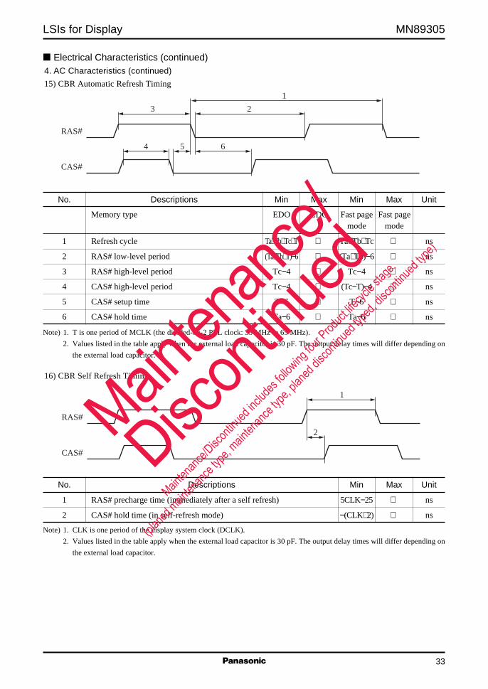
LSIs for Display MN89305
33
RAS#
CAS#
3
4 5 6
2
1
No. Descriptions Min Max Min Max Unit
Memory type EDO EDO Fast page Fast pagemode mode
1 Refresh cycle Ta+Tb+Tc+T Ta+Tb+Tc ns
2 RAS# low-level period (Ta+Tb+T)−6 (Ta+Tb)−6 ns
3 RAS# high-level period Tc−4 Tc−4 ns
4 CAS# high-level period Tc−4 (Tc−T)−4 ns
5 CAS# setup time T−6 T−6 ns
6 CAS# hold time Ta−6 Ta−6 ns
Note) 1. T is one period of MCLK (the divided-by-2 PLL clock: 35 MHz to 65 MHz).
2. Values listed in the table apply when the external load capacitor is 30 pF. The output delay times will differ depending on
the external load capacitor.
Electrical Characteristics (continued)4. AC Characteristics (continued)
15) CBR Automatic Refresh Timing
Note) 1. CLK is one period of the display system clock (DCLK).
2. Values listed in the table apply when the external load capacitor is 30 pF. The output delay times will differ depending on
the external load capacitor.
RAS#
CAS#
1
2
No. Descriptions Min Max Unit
1 RAS# precharge time (immediately after a self refresh) 5CLK−25 ns
2 CAS# hold time (in self-refresh mode) −(CLK+2) ns
16) CBR Self Refresh Timing
Mainten
ance/
Discon
tinued
Mainten
ance/D
iscont
inued
includ
es foll
owing
four P
roduct
lifecyc
le stag
e.
(planed
mainten
ance ty
pe, main
tenanc
e type,
planed
discon
tinued
typed,
discon
tinued
type)

MN89305 LSIs for Display
34
Note) 1. †1:When the LP pulse width is specified to be 1 by LCD4 and LCD5.
†2:When the number of characters on one line is set to be 84 characters by LCD0.
†3:When the time from display completion to LP generation is set to be 1 character by LCD1 and LCD4.
†4:When the time from LP completion to the 1 line completion is set to be 1 character by LCD5 and LCD0.
2. CLK is the display system clock (DCLK).
3. Values listed in the table apply when the external load capacitor is 30 pF.
Electrical Characteristics (continued)4. AC Characteristics (continued)
17) Color STN Two-Screen Panel Timing
No. Descriptions Min Max Unit
1 LP high-level period 8CLK−5†1 ns
2 FP rise to LP fall setup time 664CLK−10†2 ns
3 LP fall to FP fall hold time 8CLK−10†4 ns
4 SCK fall to LP fall setup time 19CLK−10†3 ns
5 LP fall to SCK fall hold time 9CLK−10†4 ns
6 SCL high-level period 1CLK−5 ns
7 SCK low-level period 1CLK−5 ns
8 SCK period 2CLK ns
9 UD[7:0] and LD[7:0] setup time 1CLK−10 ns
10 UD[7:0] and LD[7:0] hold time 1CLK−10 ns
LP
FP
UD[7 : 0] Line 239 Line 24 Line 1 Line 2 Line 3 Line 4 Line 5
LD[7 : 0] Line 479 Line 480 Line 241
1
Line 242 Line 243 Line 244 Line 245
SCK
SCK
LD[7 : 0]UD[7 : 0]
FP
LP
6 7 8
9 10
2 34
5
Mainten
ance/
Discon
tinued
Mainten
ance/D
iscont
inued
includ
es foll
owing
four P
roduct
lifecyc
le stag
e.
(planed
mainten
ance ty
pe, main
tenanc
e type,
planed
discon
tinued
typed,
discon
tinued
type)

LSIs for Display MN89305
35
LP
FP
UD[3 : 0] Line 239 Line 240 Line 1 Line 2 Line 3 Line 4 Line 5
LD[3 : 0] Line 479 Line 480 Line 241
1
Line 242 Line 243 Line 244 Line 245
SCK
SCK
LD[7 : 0]UD[7 : 0]
FP
LP
6 7 8
9 10
2 34
5
Electrical Characteristics (continued)4. AC Characteristics (continued)
18) Monochrome STN Two-Screen Panel Timing
Note) 1. †1:When the LP pulse width is specified to be 1 by LCD4 and LCD5.
†2:When the number of characters on one line is set to be 84 characters by LCD0.
†3:When the time from display completion to LP generation is set to be 1 character by LCD1 and LCD4.
†4:When the time from LP completion to the 1 line completion is set to be 1 character by LCD5 and LCD0.
2. CLK is the display system clock (DCLK).
3. Values listed in the table apply when the external load capacitor is 30 pF.
No. Descriptions Min Max Unit
1 LP high-level period 8CLK−5†1 ns
2 FP rise to LP fall setup time 664CLK−10†2 ns
3 LP fall to FP fall hold time 8CLK−10†4 ns
4 SCK fall to LP fall setup time 18CLK−10†3 ns
5 LP fall to SCK fall hold time 10CLK−10†4 ns
6 SCL high-level period 2CLK−5 ns
7 SCK low-level period 2CLK−5 ns
8 SCK period 4CLK ns
9 UD[7:0] and LD[7:0] setup time 2CLK−10 ns
10 UD[7:0] and LD[7:0] hold time 2CLK−10 ns
Mainten
ance/
Discon
tinued
Mainten
ance/D
iscont
inued
includ
es foll
owing
four P
roduct
lifecyc
le stag
e.
(planed
mainten
ance ty
pe, main
tenanc
e type,
planed
discon
tinued
typed,
discon
tinued
type)

MN89305 LSIs for Display
36
Note) 1. †1:When the LP pulse width is specified to be 1 by LCD4 and LCD5.
†2:When the number of characters on one line is set to be 84 characters by LCD0.
†3:When the time from display completion to LP generation is set to be 1 character by LCD1 and LCD4.
†4:When the time from LP completion to the 1 line completion is set to be 1 character by LCD5 and LCD0.
2. CLK is the display system clock (DCLK).
3. Values listed in the table apply when the external load capacitor is 30 pF.
Electrical Characteristics (continued)4. AC Characteristics (continued)
19) Color STN Single-Screen Panel Timing
No. Descriptions Min Max Unit
1 LP high-level period 8CLK−5†1 ns
2 FP rise to LP fall setup time 664CLK−10†2 ns
3 LP fall to FP fall hold time 8CLK−10†4 ns
4 SCK fall to LP fall setup time 19CLK−10†3 ns
5 LP fall to SCK fall hold time 9CLK−10†4 ns
6 SCL high-level period 1CLK−5 ns
7 SCK low-level period 1CLK−5 ns
8 SCK period 2CLK ns
9 LD[7:0] setup time 1CLK−10 ns
10 LD[7:0] hold time 1CLK−10 ns
LP
FP
LD[7 : 0] Line 479 Line 480 Line 1
1
Line 2 Line 3 Line 4 Line 5
SCK
SCK
LD[7 : 0]
FP
LP
6 7 8
9 10
2 34
5
Mainten
ance/
Discon
tinued
Mainten
ance/D
iscont
inued
includ
es foll
owing
four P
roduct
lifecyc
le stag
e.
(planed
mainten
ance ty
pe, main
tenanc
e type,
planed
discon
tinued
typed,
discon
tinued
type)
LSIs for Display MN89305
37
LP
FP
LD[7 : 0] Line 479 Line 480 Line 1
1
Line 2 Line 3 Line 4 Line 5
SCK
SCK
LD[7 : 0]
FP
LP
6 7 8
9 10
2 34
5
Electrical Characteristics (continued)4. AC Characteristics (continued)
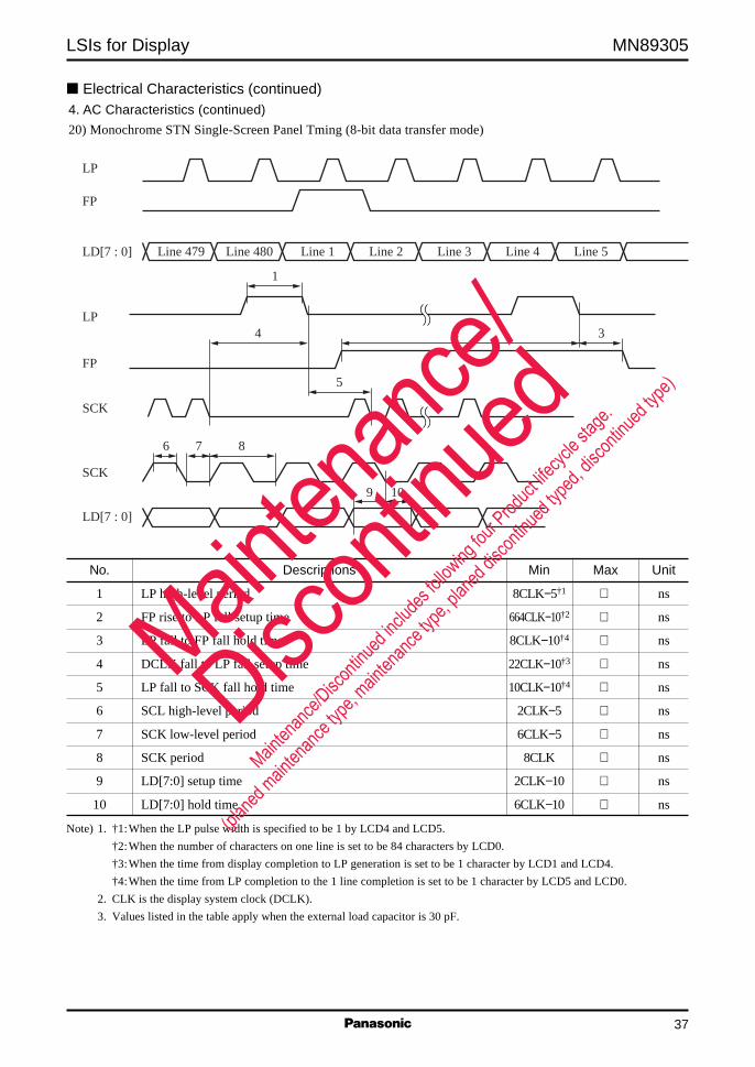
20) Monochrome STN Single-Screen Panel Tming (8-bit data transfer mode)
Note) 1. †1:When the LP pulse width is specified to be 1 by LCD4 and LCD5.
†2:When the number of characters on one line is set to be 84 characters by LCD0.
†3:When the time from display completion to LP generation is set to be 1 character by LCD1 and LCD4.
†4:When the time from LP completion to the 1 line completion is set to be 1 character by LCD5 and LCD0.
2. CLK is the display system clock (DCLK).
3. Values listed in the table apply when the external load capacitor is 30 pF.
No. Descriptions Min Max Unit
1 LP high-level period 8CLK−5†1 ns
2 FP rise to LP fall setup time 664CLK−10†2 ns
3 LP fall to FP fall hold time 8CLK−10†4 ns
4 DCLK fall to LP fall setup time 22CLK−10†3 ns
5 LP fall to SCK fall hold time 10CLK−10†4 ns
6 SCL high-level period 2CLK−5 ns
7 SCK low-level period 6CLK−5 ns
8 SCK period 8CLK ns
9 LD[7:0] setup time 2CLK−10 ns
10 LD[7:0] hold time 6CLK−10 ns
Mainten
ance/
Discon
tinued
Mainten
ance/D
iscont
inued
includ
es foll
owing
four P
roduct
lifecyc
le stag
e.
(planed
mainten
ance ty
pe, main
tenanc
e type,
planed
discon
tinued
typed,
discon
tinued
type)

MN89305 LSIs for Display
38
Note) 1. †1:When the LP pulse width is specified to be 1 by LCD4 and LCD5.
†2:When the number of characters on one line is set to be 84 characters by LCD0.
†3:When the time from display completion to LP generation is set to be 1 character by LCD1 and LCD4.
†4:When the time from LP completion to the 1 line completion is set to be 1 character by LCD5 and LCD0.
2. CLK is the display system clock (DCLK).
3. Values listed in the table apply when the external load capacitor is 30 pF.
Electrical Characteristics (continued)4. AC Characteristics (continued)
21) Monochrome STN Single-Screen Panel Timing (4-bit data transfer mode)
No. Descriptions Min Max Unit
1 LP high-level period 8CLK−5†1 ns
2 FP rise to LP fall setup time 664CLK−10†2 ns
3 LP fall to FP fall hold time 8CLK−10*4 ns
4 SCK fall to LP fall setup time 18CLK−10†3 ns
5 LP fall to SCK fall hold time 10CLK−10†4 ns
6 SCL high-level period 2CLK−5 ns
7 SCK low-level period 2CLK−5 ns
8 SCK period 4CLK ns
9 LD[3:0] setup time 2CLK−10 ns
10 LD[3:0] hold time 2CLK−10 ns
LP
FP
LD[3 : 0] Line 479 Line 480 Line 1
1
Line 2 Line 3 Line 4 Line 5
SCK
SCK
LD[3 : 0]
FP
LP
6 7 8
9 10
2 34
5
Mainten
ance/
Discon
tinued
Mainten
ance/D
iscont
inued
includ
es foll
owing
four P
roduct
lifecyc
le stag
e.
(planed
mainten
ance ty
pe, main
tenanc
e type,
planed
discon
tinued
typed,
discon
tinued
type)

LSIs for Display MN89305
39
DEN
DCLK
DEN
R [3 : 0]G[3 : 0]B [3 : 0]
R [3 : 0]G[3 : 0]B [3 : 0]
D0 D1 D2 D638 D639
FP
LP
LP
1
2
3
4
5
76
Electrical Characteristics (continued)4. AC Characteristics (continued)
22) Color TFT Timing
Note) 1. †1:DCLK is the display system clock period.
†2:When the LP pulse width is set to be 1 character wide with register settings.
†3:When the FP pulse width is set to be 1 line wide with register settings.
†4:When the width of 1 line is set to be 84 characters with register settings. (A blanking time of at least 4 characters per
horizontal line is required to assure the refresh time.)
†5:When the number of characters displayed on a single line is set to be 80 characters with register settings.
†6:The XIN duty factor is not taken into consideration when the display clock is set to be the sequencer output.
2. Values listed in the table apply when the external load capacitor is 30 pF.
No. Descriptions Min Max Unit
1 LP low-level period 8DCLK−10†2 ns
2 FP low-level period 1LP†3 ns
3 LP period 672DCLK†4 ns
4 DEN high-level period 640DCLK−10†5 ns
5 DCLK period †1 ns
6 R, G, and B data setup time 0.5DCLK−5†6 ns
7 R, G, and B data hold time 0.5DCLK−4†6 ns
Mainten
ance/
Discon
tinued
Mainten
ance/D
iscont
inued
includ
es foll
owing
four P
roduct
lifecyc
le stag
e.
(planed
mainten
ance ty
pe, main
tenanc
e type,
planed
discon
tinued
typed,
discon
tinued
type)

MN89305 LSIs for Display
40
BLANK
DCLK
BLANK
P[7 : 0]
P[7 : 0]HSYNCVSYNC
VSYNC
HSYNC
HSYNC
1
2
3
4
5
6
76
7
Electrical Characteristics (continued)4. AC Characteristics (continued)
23) External RAMDAC Mode Timing
Note) 1. †1:DCLK is the display system clock period.
†2:When the LP pulse width is set to be 1 character wide with register settings.
†3:When the FP pulse width is set to be 1 line wide with register settings.
†4:When the width of 1 line is set to be 84 characters with register settings. (A blanking time of at least 4 characters per
horizontal line is required to assure the refresh time.)
†5:When the number of characters displayed on a single line is set to be 80 characters with register settings.
†6:The XIN duty factor is not taken into consideration when the display clock is set to be the sequencer output.
2. Values listed in the table apply when the external load capacitor is 30 pF.
No. Descriptions Min Max Unit
1 HSYNC low-level period 8DCLK−10†2 ns
2 VSYNC low-level period 1HSYNC†3 ns
3 HSYNC period 672DCLK†4 ns
4 BLANK high-level period 640DCLK−10†5 ns
5 DCLK period †1 ns
6 P[7:0], BLANK, HSYNC, and VSYNC setup time 0.5DCLK−5†6 ns
7 P[7:0], BLANK, HSYNC, and VSYNC hold time 0.5DCLK−5†6 ns
Mainten
ance/
Discon
tinued
Mainten
ance/D
iscont
inued
includ
es foll
owing
four P
roduct
lifecyc
le stag
e.
(planed
mainten
ance ty
pe, main
tenanc
e type,
planed
discon
tinued
typed,
discon
tinued
type)
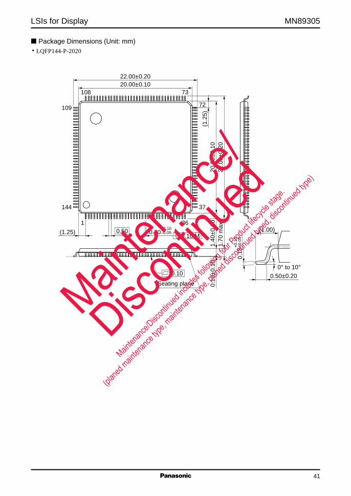
LSIs for Display MN89305
41
Package Dimensions (Unit: mm)• LQFP144-P-2020
22.00±0.2020.00±0.10
22.0
0±0.
2020
.00±
0.10
1.40
±0.1
00.
10±0
.10
1.70
max
.
(1.2
5)
108
109
144
0.20+0.10–0.05(1.25) 0.50
73
1 36(1.00)
0° to 10°0.50±0.20
72
37
0.10
Seating plane
0.10 M0.
15+
0.10
–0.0
5
Mainten
ance/
Discon
tinued
Mainten
ance/D
iscont
inued
includ
es foll
owing
four P
roduct
lifecyc
le stag
e.
(planed
mainten
ance ty
pe, main
tenanc
e type,
planed
discon
tinued
typed,
discon
tinued
type)

Request for your special attention and precautions in using the technical information andsemiconductors described in this book
(1)If any of the products or technical information described in this book is to be exported or provided to non-residents, the laws and regulations of the exporting country, especially, those with regard to security export control, must be observed.
(2)The technical information described in this book is intended only to show the main characteristics and application circuit examples of the products, and no license is granted under any intellectual property right or other right owned by our company or any other company. Therefore, no responsibility is assumed by our company as to the infringement upon any such right owned by any other company which may arise as a result of the use of technical information described in this book.
(3)The products described in this book are intended to be used for standard applications or general electronic equipment (such as office equipment, communications equipment, measuring instruments and household appliances). Consult our sales staff in advance for information on the following applications: Special applications (such as for airplanes, aerospace, automobiles, traffic control equipment, combustion equipment, life support
systems and safety devices) in which exceptional quality and reliability are required, or if the failure or malfunction of the prod-ucts may directly jeopardize life or harm the human body. Any applications other than the standard applications intended.
(4)The products and product specifications described in this book are subject to change without notice for modification and/or im-provement. At the final stage of your design, purchasing, or use of the products, therefore, ask for the most up-to-date Product Standards in advance to make sure that the latest specifications satisfy your requirements.
(5)When designing your equipment, comply with the range of absolute maximum rating and the guaranteed operating conditions (operating power supply voltage and operating environment etc.). Especially, please be careful not to exceed the range of absolute maximum rating on the transient state, such as power-on, power-off and mode-switching. Otherwise, we will not be liable for any defect which may arise later in your equipment.
Even when the products are used within the guaranteed values, take into the consideration of incidence of break down and failure mode, possible to occur to semiconductor products. Measures on the systems such as redundant design, arresting the spread of fire or preventing glitch are recommended in order to prevent physical injury, fire, social damages, for example, by using the products.
(6)Comply with the instructions for use in order to prevent breakdown and characteristics change due to external factors (ESD, EOS, thermal stress and mechanical stress) at the time of handling, mounting or at customer's process. When using products for which damp-proof packing is required, satisfy the conditions, such as shelf life and the elapsed time since first opening the packages.
(7)This book may be not reprinted or reproduced whether wholly or partially, without the prior written permission of Matsushita Electric Industrial Co., Ltd.
Mainten
ance/
Discon
tinued
Mainten
ance/D
iscont
inued
includ
es foll
owing
four P
roduct
lifecyc
le stag
e.
(planed
mainten
ance ty
pe, main
tenanc
e type,
planed
discon
tinued
typed,
discon
tinued
type)