the optical and electrical properties of bi 40 -xin se...
TRANSCRIPT
S. A. Saleh et. al. JOURNAL OF PHYSICS VOL. 1 NO. 3 Oct. (2012) PP. 9 - 14
Copyright 1996-2012 Researchpub.org. All rights Reserved. 9
Abstract — Amorphous thin films of Bi40-xInxSe60 (x =
1.6, 4.4, 7, 10 and 13.2 at.%) were deposited onto ultra
clean glass substrates by electron beam evaporation
technique at room temperature (RT). The as-deposited
films were extensively characterized by X–ray
diffraction (XRD). The composition and morphology are
determined using energy dispersive X-ray analysis
(EDS) and scanning electron microscopy (SEM). The
optical constants (namely, absorption coefficient (αααα), the
refractive index (n), extinction coefficient (k), real and
imaginary part of dielectric constant) have been studied
for as-deposited Bi40-xInxSe60 thin films as a function of
photon energy in the wavelength range 250–2500 nm at
RT. The compositional dependence of optical band gap
is discussed in light of topological and chemical ordered
network models. The temperature variation of
resistivity shows that these compounds have
semiconductor behavior.
Keywords: Amorphous thin films; Bismuth chalcogenide;
Vapor deposition; Optical properties; Electrical resistivity
I. INTRODUCTION
Amorphous multi-component chalcogenides have recently gained considerable attention due to their interesting physical properties and technological
Manuscript received June 12, 2012 and accepted Sep.30, 2012.
a Physics Department, College of Science & Arts, Najran University, P. O. 1988 Najran, Kingdom of Saudi Arabia
b Physics Department, Faculty of Science, Sohag University, Sohag 82524, Egypt * e-mail: [email protected] (S.A. Saleh) ** e-mail: [email protected] (Ihab A. Abdel-Latif) * Tel/Fax : +20934601159
applications. Among these materials, bismuth selenide as a narrow band gap semiconductors (about 0.35 eV) has attracted wide attention due to its potential applications in thermoelectric devices [1]. All possible applications emerge from their optical and electrical properties which are closely related to their structure and composition. One of the recent applications of these materials is electrical nonvolatile memory device known as chalcogenide random access memory (C-RAM) [2], which is also named phase-change memory (PCM) [3], phase-change random access memory (PCRAM [4] or PRAM [5]) or ovonic unified memory (OUM) [6]. This technology is based on reversible phase transition between crystalline (low resistivity, semi-metal) and amorphous (high resistivity, semiconductor) states. The phase change is realized via optical pulses or electrical pulses, whereas detection consists in difference of optical reflectivity or electric resistance of both phases [7].
Active materials in phase change based memories are currently chalcogenide materials [8]. The benefit of these materials consists in possibility of easily feasible reversible phase change. In addition, the rates of phase changes are high and stability of both phases in ambient conditions are relatively good. The most favorable systems are currently based on Sb-Se binary system with addition of some other elements such as Ge, In, Ag, etc. Bi-Se is also a promising material for the same applications.
Although, the physical properties of Bi2Se3 thin film have been studied [9-13], there are no data reporting optical band gap and temperature dependence of electrical resistivity of Bi-In-Se thin films. For technological application in optical and electrical memory devices, the knowledge of these properties becomes a fundamental issue.
Hence, the study of the dependence on composition of the optical and electrical properties is of great importance to improve the understanding of the mechanisms underlying these phenomena and also to improve their applications in technology. Therefore, we are interested to prepare and investigate it in the amorphous state and characterize the effect of doping BiSe with In on its physical properties.
The optical and electrical properties of Bi40-xInxSe60 thin films
S.A. Saleh* a,b
, , I. A. Abdel-Latif ** a
A. Al-Hajry a
A

S. A. Saleh et. al. JOURNAL OF PHYSICS VOL. 1 NO. 3 Oct. (2012) PP. 9 - 14
Copyright 1996-2012 Researchpub.org. All rights Reserved. 10
II. EXPERIMENTAL DETAILS
The bulk glassy material of Bi40-xInxSe60 (x = 1.6, 4.4,
7, 10 and 13.2 at.%) system was prepared by standard quenching method from Bi, In and Se of (~ 4N) purity. The necessary quantities of the elements were weighted using an electrical analytical balance with an accuracy of 10-5 gm. The weighted materials were placed in a clean sealed evacuated (10-5 Torr) silica tube. The sealed ampoules were then placed in an electric furnace and heated to a temperature of 800oC for 48 hr. The ampoules at this temperature were frequently shaken in order to homogenize the melt. After that, the ampoule was quenched into ice – cooled water.
Thin films of the present alloys were obtained from bulk samples by an electron beam evaporation technique. The deposition was carried out on ultrasonically clean glass substrate kept at 300 K by using Edward's high vacuum coating unit model E306A. The deposition parameters were kept constant for all investigated films. The film thickness was measured by a digital thickness monitor (TM200
Maxtek) and was found to be approximately 200 nm. The chemical composition of the investigated samples were determined using field emission scanning electron microscope (Joel JSM 7600F) equipped with energy dispersive spectroscopy (EDS). The amorphous nature of films was confirmed using X-ray diffractometer, type PANalytical (X' pert Pro MPR). To study the optical characteristics of the film, transmittance T(λ) and reflectance R(λ) were measured using a double beam JASCO V-570, UV–Vis–NIR spectrophotometer in the wavelength range 250–2500 nm. The spectra were recorded at normal incidence and at room temperature. The resistivity measurements were done using two probe method in the temperature range 300 – 490 K as previously reported [14].
III. RESULTS AND DISCUSSIONS
Morphological inspections performed by SEM on as–
grown films have shown a flat surface without the presence of cracks agglomerates and precipitates (Fig.1). SEM image has confirmed the absence of spurious phase. The EDS results compositional analysis for all films is close to the nominal composition. Fig. (2) illustrates the X–ray diffraction patterns of Bi40-xInxSe60 (1.6 < x < 13.2) as-deposited thin films. The absence of sharp diffraction lines and the presence of humps only confirm the amorphous nature of the prepared films. In other words, it is seen that all films are in the amorphous state where no characteristic crystalline peaks can be observed. The amorphous state was expected for the evaporated films since the quenching rate
during the deposition process is much higher than that of the melt–quench alloys [15].
Fig. (1) SEM image of Bi38.4In1.6Se60 thin film
10 20 30 40 50 60 70 80
2θθθθ o
Inte
nsit
y (
Arb
. u
n.)
Fig. (2) X-ray diffractogram of Bi2-xInxSe3 (0.08 ≤ x ≤
0.66) thin films. Study of the optical properties of Bi40-xInxSe60 (1.6 < x
< 13.2) films, particularly the absorption edge gives valuable information on the electronic structure of the material. The optical behavior of the material is generally utilized to determine its optical constants i.e. refractive index (n), extinction coefficient (k), real (ε') and imaginary (ε'') parts of the dielectric constant.

S. A. Saleh et. al. JOURNAL OF PHYSICS VOL. 1 NO. 3 Oct. (2012) PP. 9 - 14
Copyright 1996-2012 Researchpub.org. All rights Reserved. 11
The variation of the absorption coefficient (α) as a function of incident photon energy (hν) for deposited films is shown in Fig. (3). It was computed by the following expression [16-18] : α = OD /d where OD is the optical density measured at a given layer thickness (d).
0
0.5
1
1.5
2
2.5
3
3.5
0.8 1 1.2 1.4 1.6 1.8 2 2.2
hν ν ν ν (ev)
αα αα (
10
6)(
cm
-1)
In=1.6
In=4.4
In=7
In=10
In=13.2
Fig. 3 Plot of absorption coefficient with photon energy
for as-prepared films.
It has been observed that the values of α increases with
the increase in photon energy for all films. In the high absorption region (α ≥ 104 cm-1), the absorption coefficient can be described by the relation [19 – 21] which is often
called Tauc's law ( )ropt
gEhh −= νβνα where hν
is the incident photon energy, The edge width parameter β representing the film quality, Eg
opt is the optical band gap of a material and the power r is a number characterizing the type of optical transition process. The parameter r has the values of 2, and 0.5 depending on the nature of the electronic transition responsible for absorption: r = 0.5 allowed direct optical transition and r = 2 for allowed indirect optical transition. Plotting the (αhν)1/r versus photon energy (hν) and assuming an allowed direct type electron transition (r = 0.5), as is the case for chalcogenide materials, the optical band gap Eg
opt was determined near the absorption edge by extrapolating the linear part of the curves toward zero absorption; the interception with the photon energy axis providing the Eg
opt value. The results are summarized in Fig. 4, where the plot of (αhν)2 versus (hν) is given for all as-deposited films. The calculated values of Eg
opt are given in Table 1. The value of the optical band gap decreases with increasing In concentration until specific value after that it slightly decrease. The change in the optical band gap could be discussed on the basis of density of state model proposed by Mott and Davis [22]. According to this, the width of the localized states near the mobility edges depends on the degree of disorder and
defects present in the amorphous structure. In particular, it is known that the unsaturated bonds are responsible for the
1.00E+11
6.00E+11
1.10E+12
1.60E+12
2.10E+12
2.60E+12
3.10E+12
1.8 1.9 2 2.1 2.2 2.3 2.4 2.5 2.6 2.7 2.8
hν (ν (ν (ν (ev)
( αα ααh
νν νν)2
(cm
-1e
v)2
S1
S2
S3
S4
S5
Fig. 4 Plot of (ααααhνννν)
2 vs. hνννν for different films.
formation of some defects in amorphous solids. Such defects produce localized states in the band structure. The presence of a high concentration of localized states is responsible for relatively low values of the optical band gap in the case of as-deposited amorphous films [23]. The decrease of Eg
opt values with increasing the In content can be also explained on the bases of the suggestion that the change of the band gap is caused by alloying effect, namely a compositional change in the host material itself [21] due to the change in bond angle and/or bond lengths modifying the glassy structure and disturbing the ordering. The optical band gap value is correlated with the average coordination number (Z). Average coordination number Z of a ternary InαBiβSeγ system is defined by the expression [24]:
γβα
γβα
++
++=
234Z where α, β, and γ are the
atomic percentages of In, Bi and Se, while 4, 3, and 2 their coordination number. The coordination number Z characterizes the electronic properties of semiconducting materials, and shows the bonding character in the nearest-neighbor region [25]. According to the constrain theory [26], the investigated compositions are over-coordinated, stressed-rigid and with lower connectivity, as the values of Z are larger than 2.4. These observations indicate that the effects of chemical ordering are also present in this system along with the overall topological effects.
The knowledge of accurate values of wavelength dependence refractive index and extinction coefficient of chalcogenide thin film is very important for both fundamental and technological point of view. Moreover, refractive index is necessary for the design and modeling of optical components and optical coating such as interference filters. The theory of reflectance of light from a thin film is

S. A. Saleh et. al. JOURNAL OF PHYSICS VOL. 1 NO. 3 Oct. (2012) PP. 9 - 14
Copyright 1996-2012 Researchpub.org. All rights Reserved. 12
expressed in terms of Fresnel's coefficient. The values of refractive index (n), and extinction coefficient (k) for the examined films were computed from the obtained R(λ) using the following relations [27],
,4 π
αλ=k ( )
2
1
22
111
11
+−
−
+±
−
+= k
R
R
R
Rn
where R is reflectance or reflectivity. The real (ε') and imaginary (ε'') parts of the dielectric constant for Bi40-xInxSe60 thin films can be calculated with the help of refractive index (n) and extinction coefficient (k) by using the relation [28], ε' = n2 - k2 and ε''= 2nk. The variation of these two parameters with photon energy is shown in Fig. (5) and (6). for all investigated film compositions. It is evident from Fig. (5) and (6) that the value of ε' and ε'' both decreases with the increase in photon energy for all films.
30
50
70
90
110
0.59 0.615 0.64 0.665
hνννν (ev)
εε εε'
In=1.6 In=4.4 In=7 In=10 In=13.2
Fig. (5) εεεε' versus hνννν for as-deposited thin films.
10
15
20
25
30
35
40
0.59 0.6 0.61 0.62 0.63 0.64 0.65 0.66
hνννν (ev)
εε εε''
In=1.6 In=4.4 In=7 In=10 In=13.2
Fig. 6. εεεε'' versus hν ν ν ν for all films
Electrical measurements The dark electrical resistivity of the thin films with different concentrations was measured in the temperature 300–500 K. A plot of inverse absolute temperature versus loge (resistivity) for a warming cycle is shown in Fig.7.
-5
5
15
25
35
45
300 320 340 360 380 400 420 440 460 480
T(K)
ρρ ρρ( ΩΩ ΩΩ
cm
)
-0.5
0
0.5
1
1.5
2
2.5
3
ρρ ρρ( ΩΩ ΩΩ
cm
)
In=1.6 In=4.4
In=10 In=13.2
Fig. 7 Temperature dependence of resistivity for the
present system.
The curves show a linear decrease in the resistivity with the increase in temperature up to a point where a sudden decrease takes place, which indicates the crystallization of the amorphous films (crystallization temperature Tc). Below Tc, the resistivity decreases at a much lower rate than in the amorphous materials, although this decrease is more pronounced in samples with higher In concentration. Two distinct regions of ρ(T) corresponding to low and high temperature ranges are observed i.e. it is evident from these
S. A. Saleh et. al. JOURNAL OF PHYSICS VOL. 1 NO. 3 Oct. (2012) PP. 9 - 14
Copyright 1996-2012 Researchpub.org. All rights Reserved. 13
curves that the conduction has two different mechanisms. In high temperature region the abrupt decrease in ρ means that the conduction is thermally activated and can be obeyed the following Arrhenius equation:
)/exp()( TKET o βρρρ =
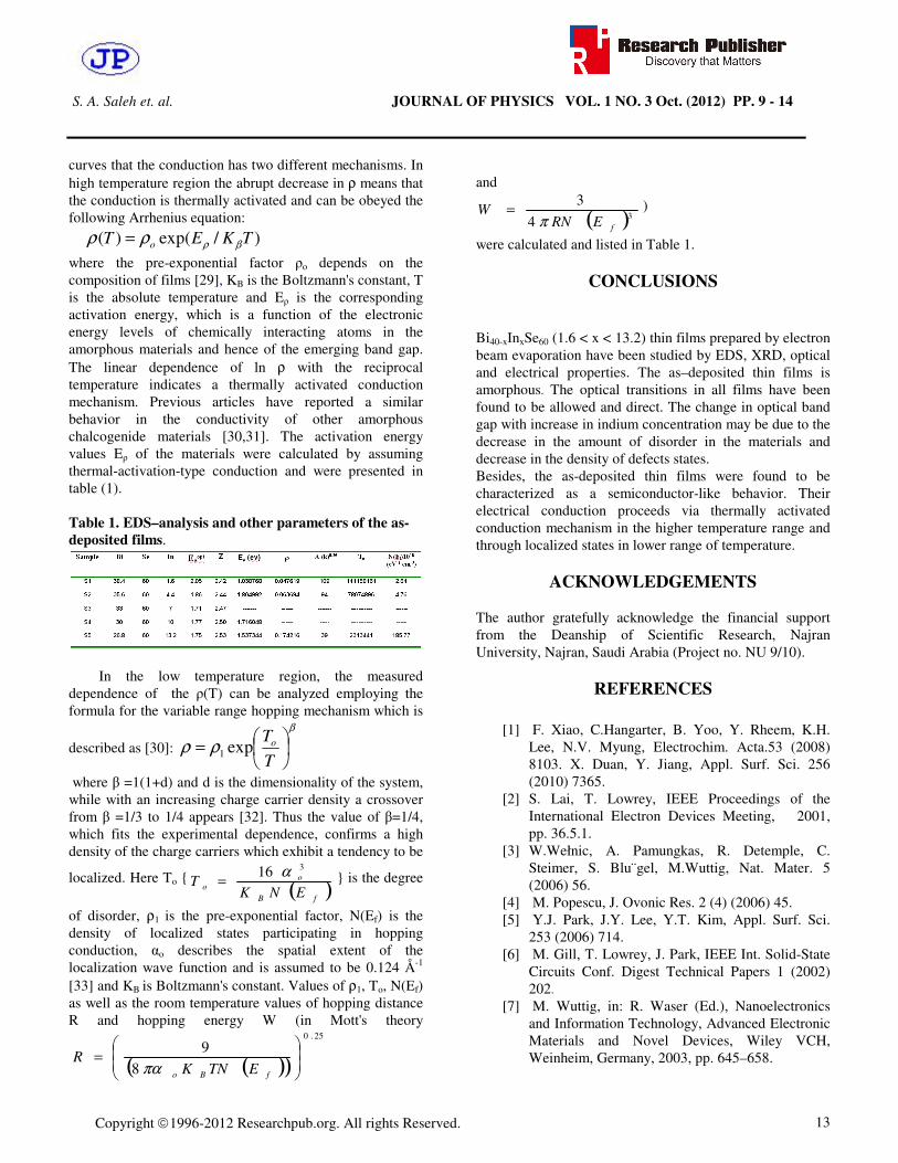
where the pre-exponential factor ρo depends on the composition of films [29], KB is the Boltzmann's constant, T is the absolute temperature and Eρ is the corresponding activation energy, which is a function of the electronic energy levels of chemically interacting atoms in the amorphous materials and hence of the emerging band gap. The linear dependence of ln ρ with the reciprocal temperature indicates a thermally activated conduction mechanism. Previous articles have reported a similar behavior in the conductivity of other amorphous chalcogenide materials [30,31]. The activation energy values Eρ of the materials were calculated by assuming thermal-activation-type conduction and were presented in table (1).
Table 1. EDS–analysis and other parameters of the as-
deposited films.
In the low temperature region, the measured dependence of the ρ(T) can be analyzed employing the formula for the variable range hopping mechanism which is
described as [30]:
β
ρρ
=
T
Toexp1
where β =1(1+d) and d is the dimensionality of the system, while with an increasing charge carrier density a crossover from β =1/3 to 1/4 appears [32]. Thus the value of β=1/4, which fits the experimental dependence, confirms a high density of the charge carriers which exhibit a tendency to be
localized. Here To ( )
fB
oo
ENKT
316 α= is the degree
of disorder, ρ1 is the pre-exponential factor, N(Ef) is the density of localized states participating in hopping conduction, αo describes the spatial extent of the localization wave function and is assumed to be 0.124 Å-1 [33] and KB is Boltzmann's constant. Values of ρ1, To, N(Ef) as well as the room temperature values of hopping distance R and hopping energy W (in Mott's theory
( )( )
25.0
89
=
fBo ETNKR
πα
and
( )34
3
fERNW
π= )
were calculated and listed in Table 1.
CONCLUSIONS
Bi40-xInxSe60 (1.6 < x < 13.2) thin films prepared by electron beam evaporation have been studied by EDS, XRD, optical and electrical properties. The as–deposited thin films is amorphous. The optical transitions in all films have been found to be allowed and direct. The change in optical band gap with increase in indium concentration may be due to the decrease in the amount of disorder in the materials and decrease in the density of defects states. Besides, the as-deposited thin films were found to be characterized as a semiconductor-like behavior. Their electrical conduction proceeds via thermally activated conduction mechanism in the higher temperature range and through localized states in lower range of temperature.
ACKNOWLEDGEMENTS The author gratefully acknowledge the financial support from the Deanship of Scientific Research, Najran University, Najran, Saudi Arabia (Project no. NU 9/10).
REFERENCES
[1] F. Xiao, C.Hangarter, B. Yoo, Y. Rheem, K.H.
Lee, N.V. Myung, Electrochim. Acta.53 (2008) 8103. X. Duan, Y. Jiang, Appl. Surf. Sci. 256 (2010) 7365.
[2] S. Lai, T. Lowrey, IEEE Proceedings of the International Electron Devices Meeting, 2001, pp. 36.5.1.
[3] W.Wełnic, A. Pamungkas, R. Detemple, C. Steimer, S. Blu¨gel, M.Wuttig, Nat. Mater. 5 (2006) 56.
[4] M. Popescu, J. Ovonic Res. 2 (4) (2006) 45. [5] Y.J. Park, J.Y. Lee, Y.T. Kim, Appl. Surf. Sci.
253 (2006) 714. [6] M. Gill, T. Lowrey, J. Park, IEEE Int. Solid-State
Circuits Conf. Digest Technical Papers 1 (2002) 202.
[7] M. Wuttig, in: R. Waser (Ed.), Nanoelectronics and Information Technology, Advanced Electronic Materials and Novel Devices, Wiley VCH, Weinheim, Germany, 2003, pp. 645–658.

S. A. Saleh et. al. JOURNAL OF PHYSICS VOL. 1 NO. 3 Oct. (2012) PP. 9 - 14
Copyright 1996-2012 Researchpub.org. All rights Reserved. 14
[8] G.F. Zhou, Mater. Sci. Eng. A – Struct. Mater. Prop. Microstruct. Process. 304(Spec. Iss.) (2001) 73.
[9] R.H. Bari, L.A. Patil, Ind. J. of Pure& App. Phys. 48 (2010) 127 – 132.
[10] S. Subramanian, D.P. Padiyan, Mater. Chem. Phys. 107 (2008) 392 – 398.
[11] S. Augustine, S. Ampili, J.K. Kang, E. Mathai, Mater. Res. Bull. 40 (2005) 1314 – 1325.
[12] B. Pejova, I. Grozdanov, A. Tanusevski, Mater. Chem. Phys. 83 (2004) 245 – 249.
[13] B. Pejova, I. Grozdanov, Thin Solid Films 408 (2002) 6 – 10.
[14] S.A. Saleh, A. A. Hendi, I. A. Abdel-Latif, J. of American Science 7 (2011) 923-928.
[15] A.H. Moharram Appl. Phys. A 66 (1998) 515. [16] A. A. Al-Ghamdi, S.A. Khan, Physica B 404
(2009) 426. [17] S.A. Khan, et al., Physica B 405 (2010) 3348. [18] S. A. Khan, A. A. Al-Ghamdi, Mater. Lett. 63
(2009) 1740. [19] J. Tauc, Amorphous and Liquid Semiconductors,
London and New York: Plenum Press ; 1974. [20] G. Saffarini, J.M. Saiter, H. Schmitt, Optical
Mater. 29 (2007) 1143-1147. [21] V. Pamukchieva, et al., Optical Mater. 32 (2009)
45-48. [22] N.F. Mott, E.A. Davis, Electronic Processes in
Non-crystalline Materials, Clarendon Press, Oxford, (1979) 428.
[23] M. Fadel, S.A. Fayek, M.O. Abou-Helal, M.M. Ibrahim, A.M. Shakra, J.Alloys and Compounds 485 (2009) 604.
[24] S.A. Saleh A. Al-Hajry, H. M. Ali, Phys. Scr. 84 (2011) 015604.
[25] S.A. Saleh, Mate. Sci. Appl. 2 (2011) 950. [26] J.C. Phillips, M.F. Thorpe, Solid State Commun.
53 (1985) 699. [27] H. A. Mohamed, and H. M. Ali, Sci. Technol.
Adv. Mater. 9 (2008) 025016. [28] M. M. Wakkad, E. Kh. Shoker, S. H. Mohamed, J.
Non-Cryst. Solids 265 (2000) 157. [29] E. Prokhorov A. Mendoza-Galvan, J. Gonzalez-
Hernandez, B. Chao, J. Non-Crystalline Solids 353 (2007) 1870–1874.
[30] N.F. Mott, E.A. Davis, Electronic Processes in Non-crystalline Materials, Clarendon Press, Oxford, 1978.
[31] H. Fritzsche, in: J. Tauc (Ed.), Amorphous and Liquid Semiconductors, Plenum Press, London, New York, 1974, p. 221.
[32] N.F. Mott, Philos. Mag. 22 (1970) 7. [33] S.A. Ahmed, E.M.M. Ibrahim, S.A. Saleh, Appl.
Phy. A 85 (2006) 177 – 184.