the reactive bridge: a novel solid-state low … reactive bridge: a novel solid-state low energy...
TRANSCRIPT
The Reactive Bridge: A NovelSolid-State Low Energy Initiator
Dr. Thomas A. Baginski (Auburn University)David Fahey (Quantic Industries)

Report Documentation Page
Report Date 16Apr2001
Report Type N/A
Dates Covered (from... to) -
Title and Subtitle The Reactive Bridge: A Novel Solid-State Low Energy Initiator
Contract Number
Grant Number
Program Element Number
Author(s) Baginski, Thomas A. ; Fahey, David
Project Number
Task Number
Work Unit Number
Performing Organization Name(s) and Address(es) Auburn University
Performing Organization Report Number
Sponsoring/Monitoring Agency Name(s) and Address(es) NDIA (National Defense Industrial Assocation) 211Wilson BLvd., Ste. 400 Arlington, VA 22201-3061
Sponsor/Monitor’s Acronym(s)
Sponsor/Monitor’s Report Number(s)
Distribution/Availability Statement Approved for public release, distribution unlimited
Supplementary Notes Proceedings from The 45th Annual Fuze Conference, 16-18 April 2001 Sponsored by NDIA, The originaldocument contains color images.
Abstract
Subject Terms
Report Classification unclassified
Classification of this page unclassified
Classification of Abstract unclassified
Limitation of Abstract UU
Number of Pages 27
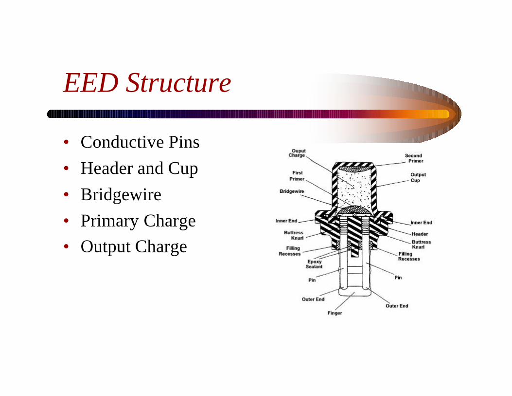
EED Structure
• Conductive Pins• Header and Cup• Bridgewire• Primary Charge• Output Charge
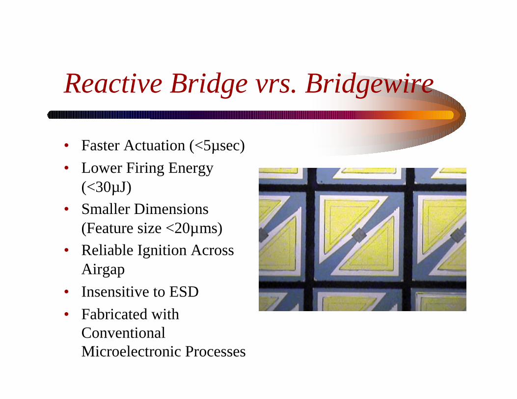
Reactive Bridge vrs. Bridgewire
• Faster Actuation (<5µsec)• Lower Firing Energy
(<30µJ)• Smaller Dimensions
(Feature size <20µms)• Reliable Ignition Across
Airgap• Insensitive to ESD• Fabricated with
ConventionalMicroelectronic Processes
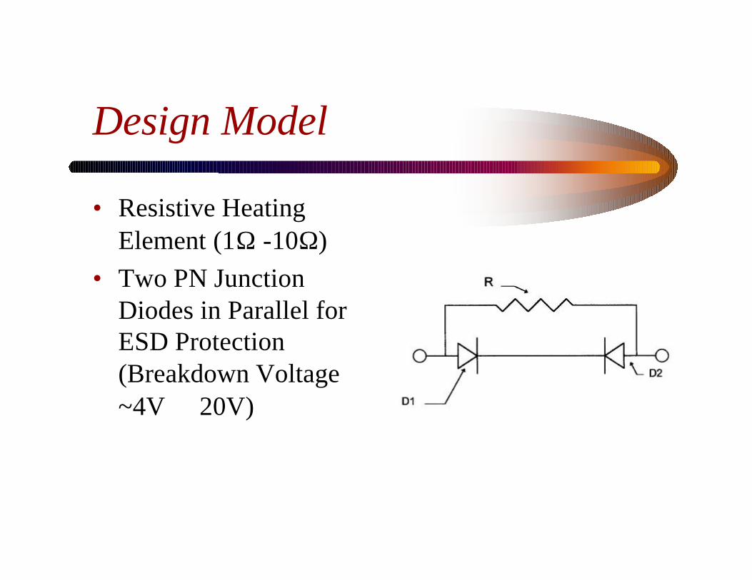
Design Model
• Resistive HeatingElement (1Ω -10Ω)
• Two PN JunctionDiodes in Parallel forESD Protection(Breakdown Voltage~4V ⇔20V)

Composite Reactive BridgeFabrication
• Utilizes Basic Fabrication Techniques• Photolithography• Wet Chemical Etching• Sputtering and E-beam Metal Deposition• Liftoff Process
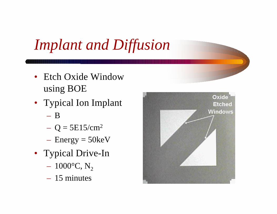
Implant and Diffusion
• Etch Oxide Windowusing BOE
• Typical Ion Implant– B– Q = 5E15/cm2
– Energy = 50keV
• Typical Drive-In– 1000°C, N2
– 15 minutes

Aluminum Deposition
• Sputter ~12,000Å ofSi/Al
• Mask off Window• Etch Al with PAE• Etch Residual Si• Alloy Al at 450°C for
30 minutes

Palladium Deposition
• Mask and Develop• Deposit
– 500Å of Ti– 2000Å of Pd
• Liftoff– Ultrasonic and Acetone

Gold Deposition
• Mask and Develop• Deposit
– 500Å of Ti– 1000Å of Ni– 2000Å of Au
• Liftoff– Ultrasonic and Acetone

Zirconium Deposition/ReactiveOvercoat
• Mask and Develop• Deposit
– 500Å of Ti– 10,000Å of Zr
• Additional Mass forPlasma Formation
• Chemically Reactive• Liftoff
– Ultrasonic and Acetone
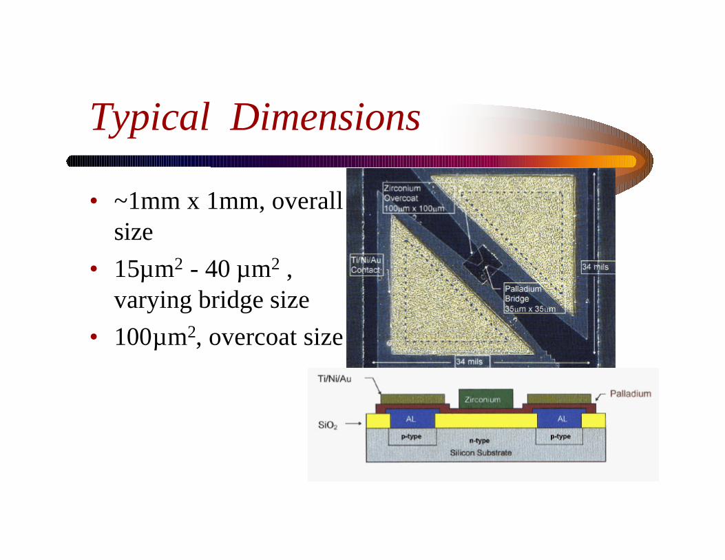
Typical Dimensions
• ~1mm x 1mm, overallsize
• 15µm2 - 40 µm2 ,varying bridge size
• 100µm2, overcoat size

Packaging
• ValoxDR48 PlasticHeader
• Conducting Pins• Output Cup
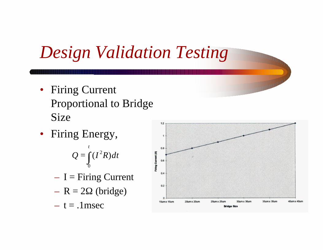
Design Validation Testing
• Firing CurrentProportional to BridgeSize
• Firing Energy,
– I = Firing Current– R = 2Ω (bridge)– t = .1msec
∫=t
dtRIQ0
2 )(
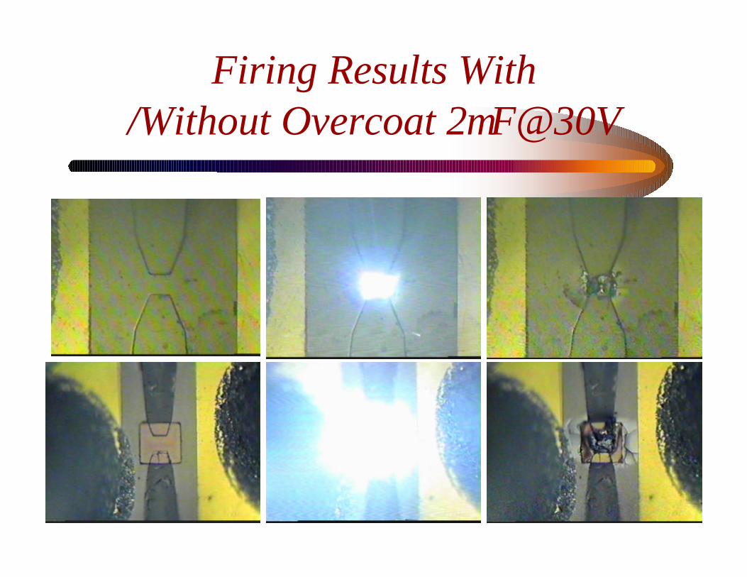
Firing Results With/Without Overcoat 2µF@30V
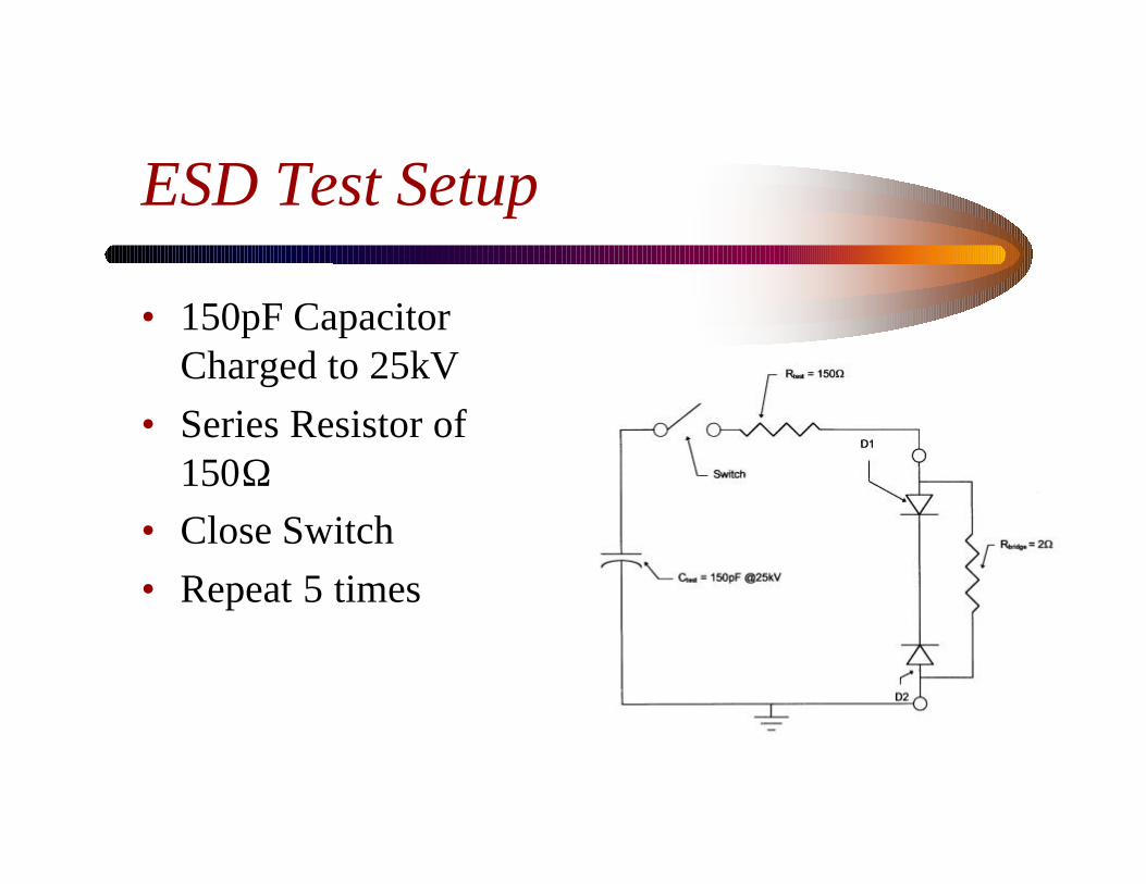
ESD Test Setup
• 150pF CapacitorCharged to 25kV
• Series Resistor of150Ω
• Close Switch• Repeat 5 times

Environmental Test Setup
• 320 Parts• High Temp, 144 hrs @ 107°C• Thermal Shock and Humidity
– 6 cycles(-40°C and 107°C) for 12 hrs
• RandomVibration– Method S14:4 category I– 3 perpendicular axis, -40°C, 21°C, and 90°C
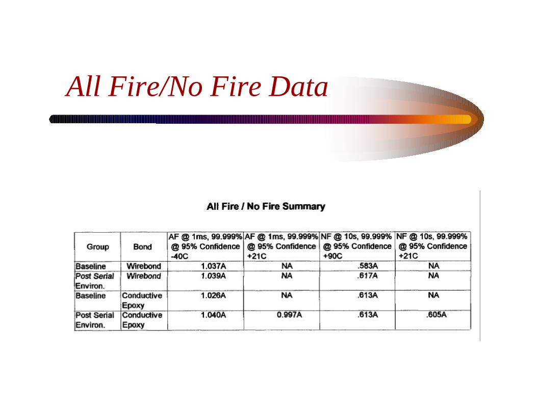
All Fire/No Fire Data
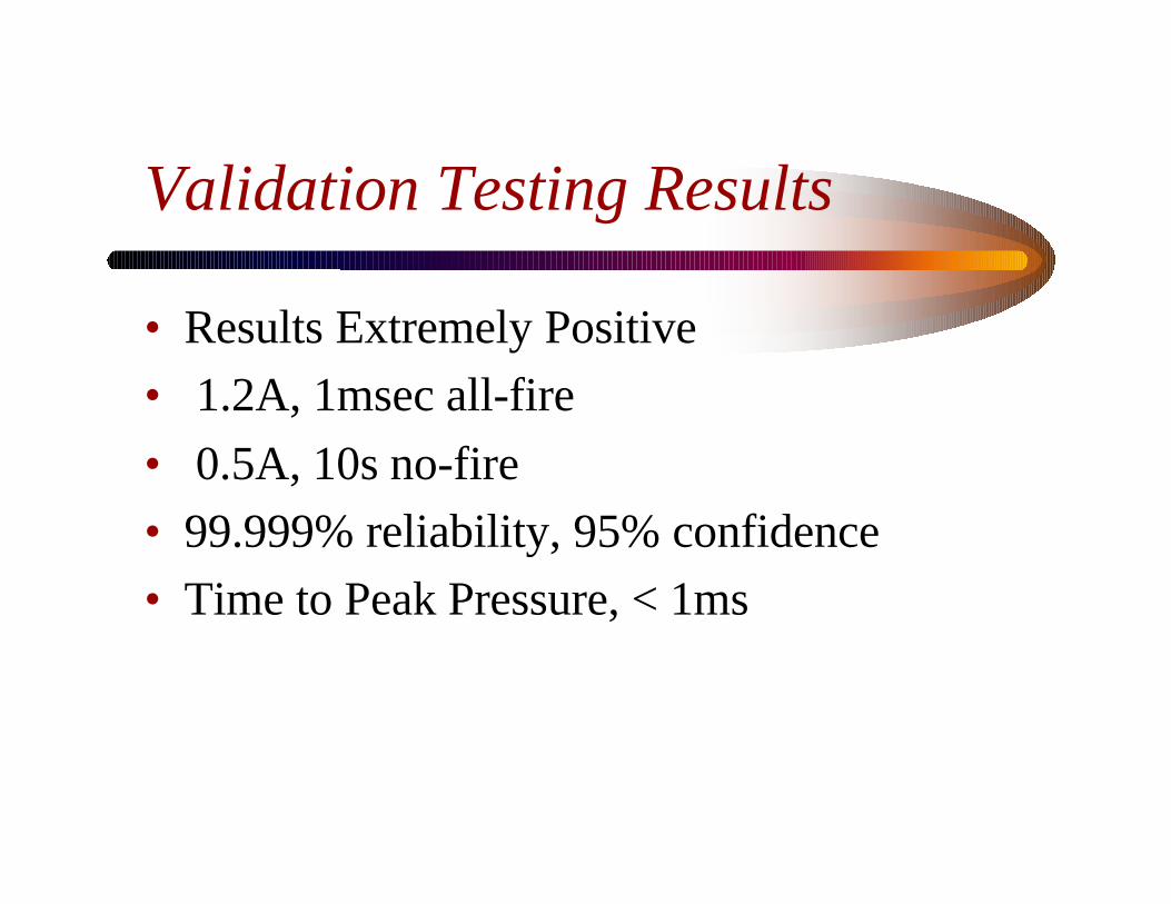
Validation Testing Results
• Results Extremely Positive• 1.2A, 1msec all-fire• 0.5A, 10s no-fire• 99.999% reliability, 95% confidence• Time to Peak Pressure, < 1ms
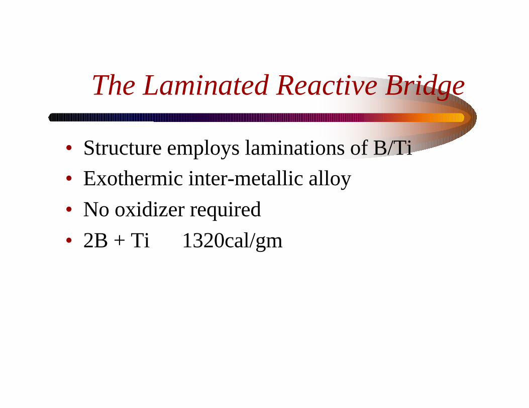
The Laminated Reactive Bridge
• Structure employs laminations of B/Ti• Exothermic inter-metallic alloy• No oxidizer required• 2B + Ti ⇒ 1320cal/gm

Laminated Reactive Bridge
Ti/Ni/Au
Ti/B/Ti/BTi/B/Ti/B/TiSilicon
Dioxide
Topview
Sideview
Silicon Substrate
SiliconDioxide
Titanium
Boron
Ti/Ni/Au
DiodeAl

Sample Firing Of Laminated110µm Bridge 35µF@30V
4cm 4cm
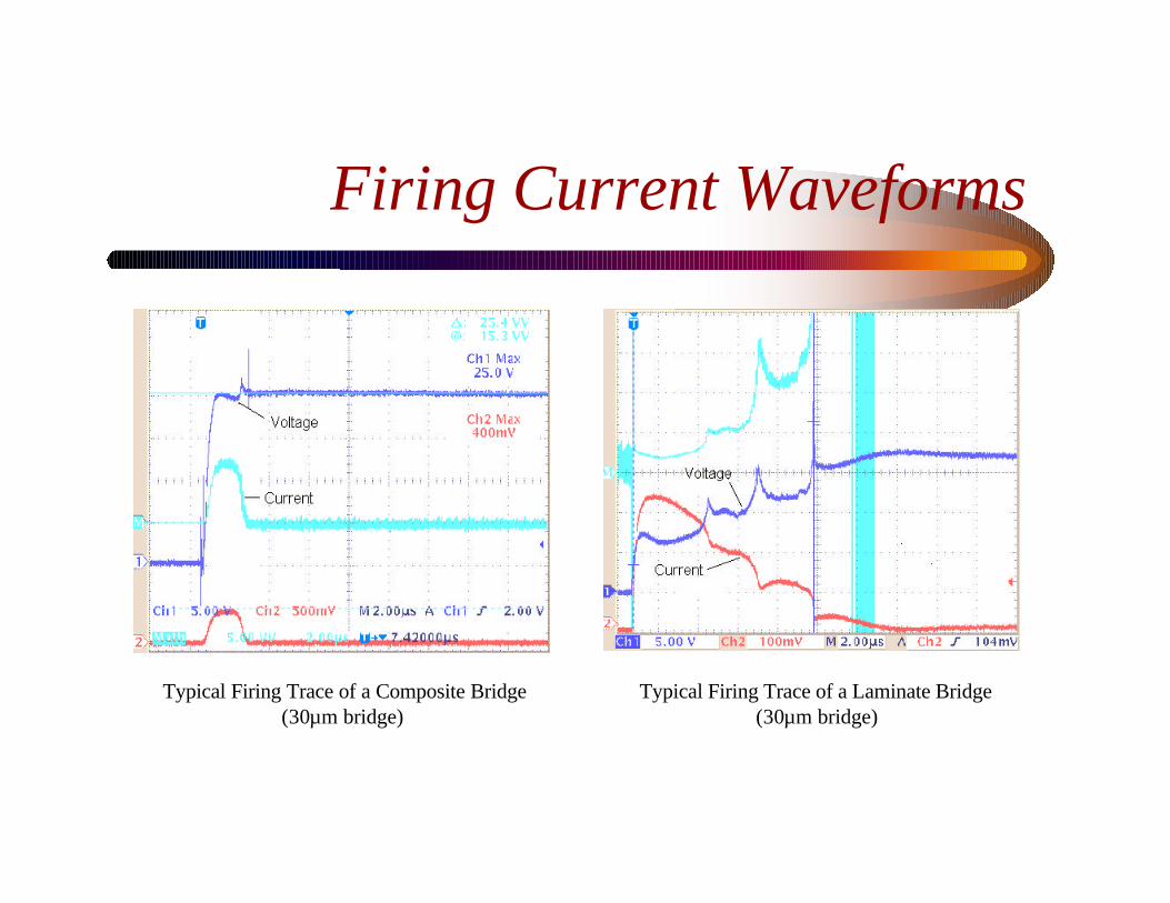
Firing Current Waveforms
Typical Firing Trace of a Laminate Bridge(30µm bridge)
Typical Firing Trace of a Composite Bridge(30µm bridge)

Firing Characteristics ofLaminated Bridge with 5Ω ESR
MEAN FIRING VOLTAGE AND ENERGY VERSUS CAPACITOR SIZE
0
5
10
15
20
25
0 5 10 15 20 25
CAP SIZE (uf)
VO
LTA
GE
(V
)
0
20
40
60
80
100
120
140
160
180
200
EN
ER
GY
(uj
)
Capacitor (V)
Energy (uj)
A plot of firing voltage and energy for a 20 µm Laminated bridge

Firing Data for Laminated Bridge
Reactive SCB Mean Firing Voltage Vs Capacitance & Bridge Size
0
5
10
15
20
25
0 20 40 60
Firing Capacitor - microfarads
Mea
n F
irin
g V
olt
age
- vo
lts
1.4 ohm 10x10u1.2 ohm 30x30u1 ohm 50x50u0.89 ohm 70x70u0.906 ohm 90x90u0.753 ohm 110x110u
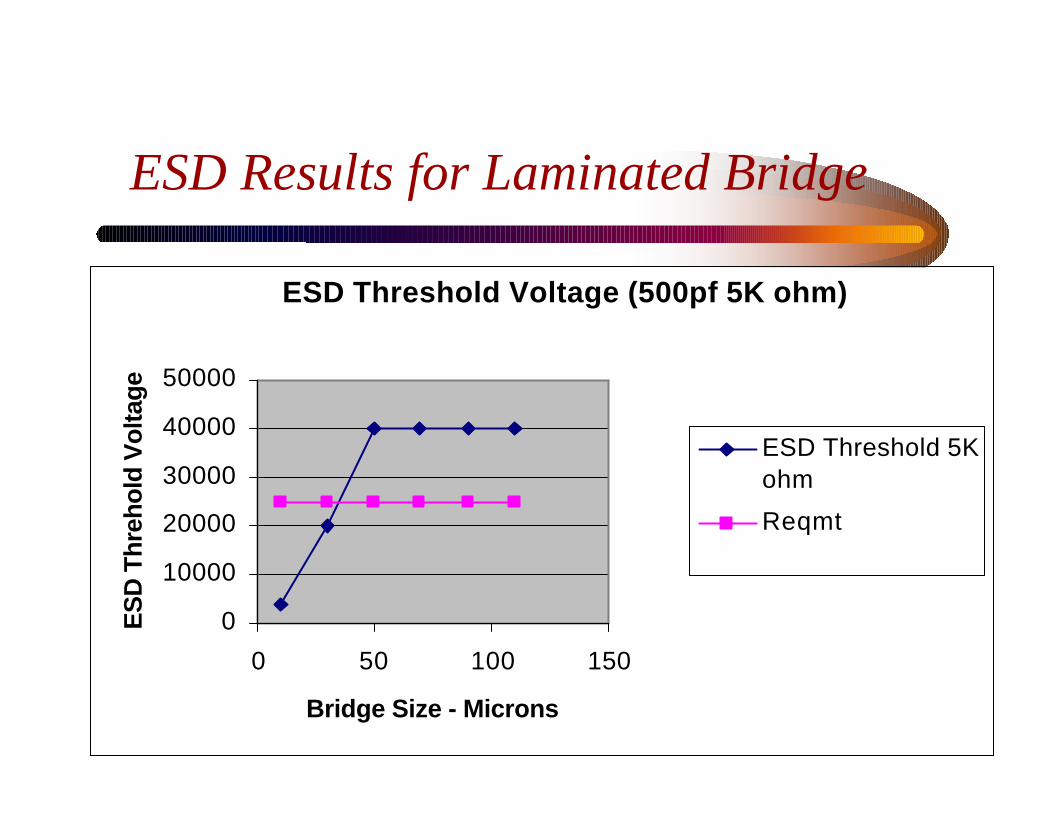
ESD Results for Laminated Bridge
ESD Threshold Voltage (500pf 5K ohm)
0
10000
20000
30000
40000
50000
0 50 100 150
Bridge Size - Microns
ES
D T
hreh
old
Vol
tage
ESD Threshold 5Kohm
Reqmt
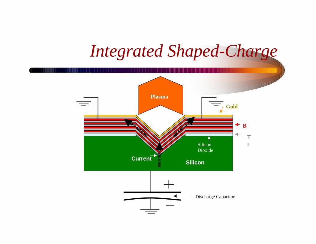
Integrated Shaped-Charge
Ti
Gold
B
SiliconCurrent
Plasma
Discharge Capacitor
SiliconDioxide
Conclusion
• Devices Fabricated Using ConventionalTechniques
• Demonstrates Lower Firing Energy• Diodes Protect Against ESD Events• Reliably Fires in Less Than 1µsec• Plasma Output Capable of Jumping a Gap• Very Economical for Large Volumes