the serial peripheral interface (spi) lecture l4.5
Post on 22-Dec-2015
229 views
TRANSCRIPT
The Serial Peripheral Interface (SPI)
Lecture L4.5
Reference
SPIBlock GuideV03.06
S12SPIV3.pdf
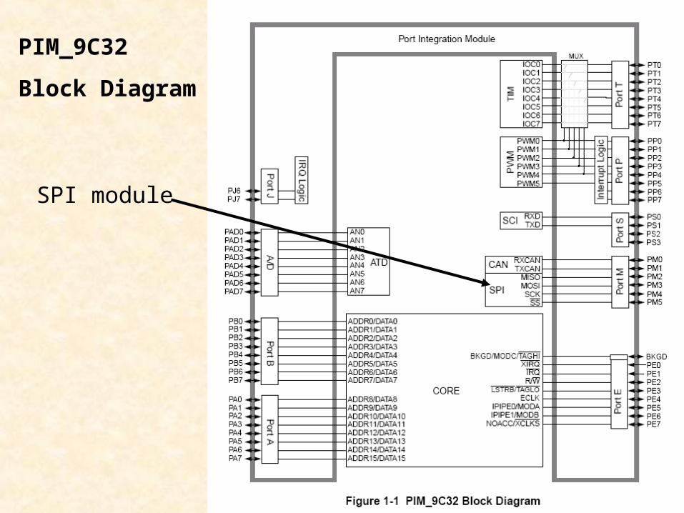
PIM_9C32
Block Diagram
SPI module
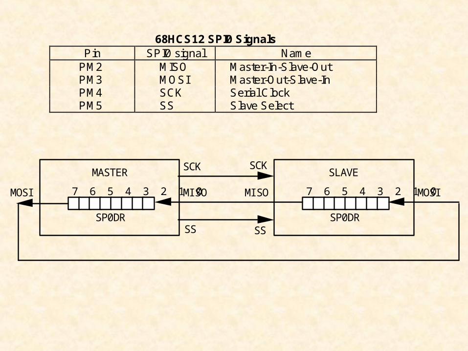
68HCS12 SPI0 Signals Pin SPI0 signal Name
PM2 MISO Master-In-Slave-Out PM3 MOSI Master-Out-Slave-In PM4 SCK Serial Clock PM5 SS Slave Select
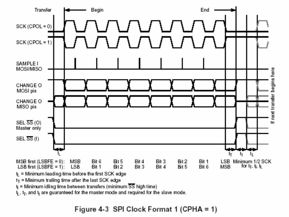
7 6 5 4 3 2 1 0
SP0DR
MASTER
7 6 5 4 3 2 1 0
SP0DR
SLAVE
MOSI MOSIMISO MISO
SCK
SS SS
SCK
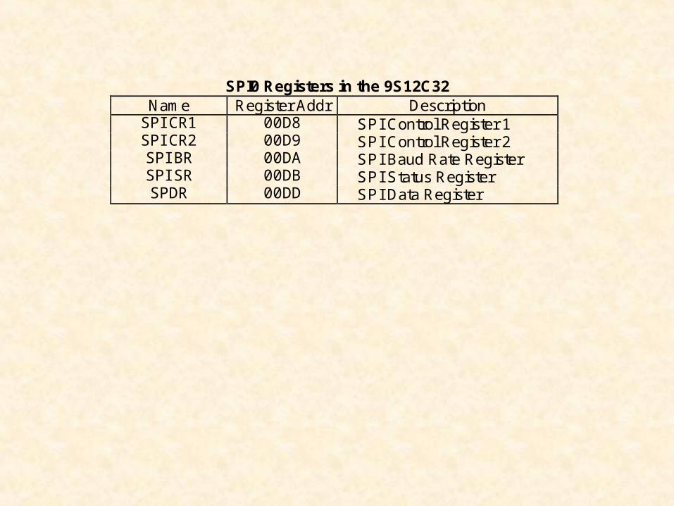
SPI0 Registers in the 9S12C32 Name Register Addr Description SPICR1 00D8 SPI Control Register 1 SPICR2 00D9 SPI Control Register 2 SPIBR 00DA SPI Baud Rate Register SPISR 00DB SPI Status Register SPDR 00DD SPI Data Register
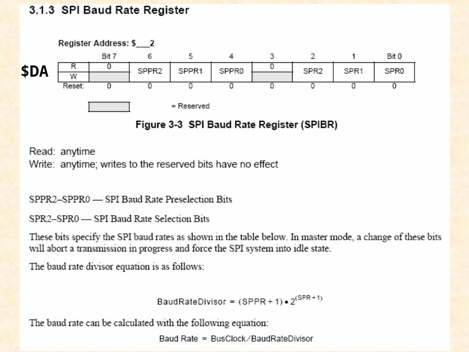
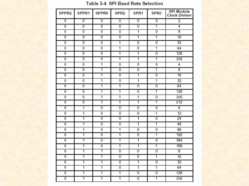
$DA
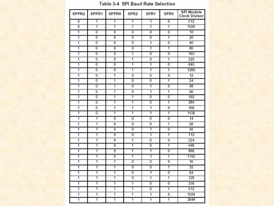
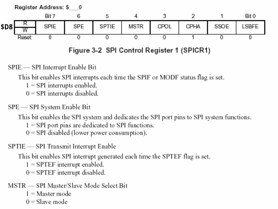
$D8
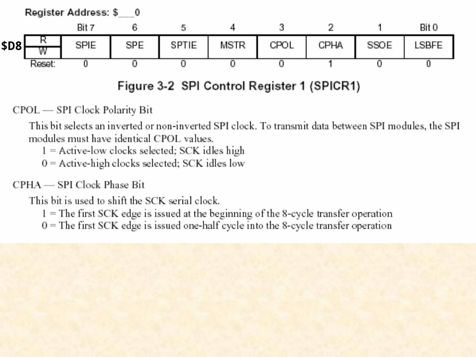
$D8
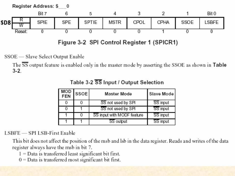
$D8
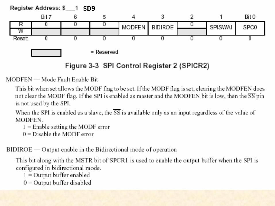
$D9
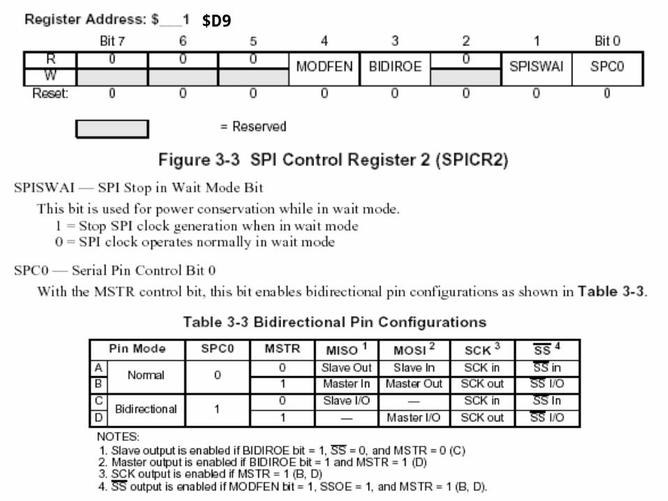
$D9
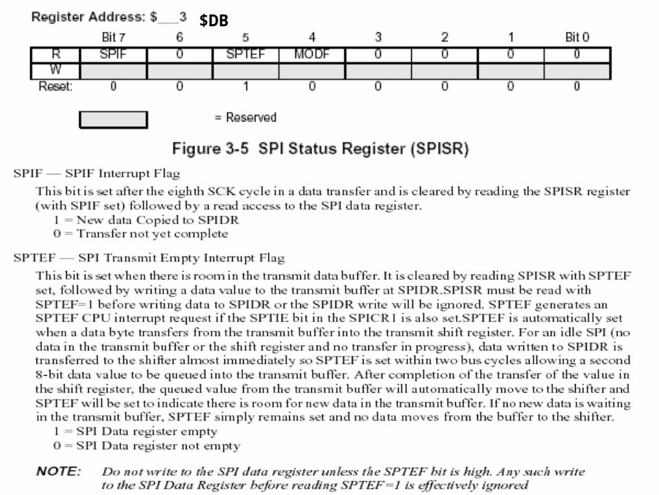
$DB
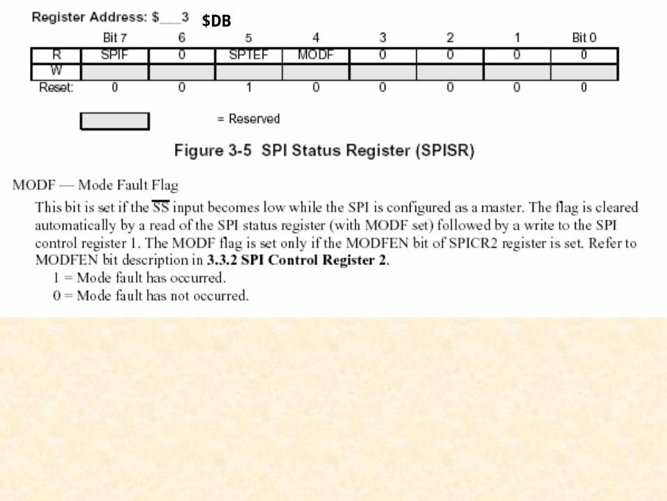
$DB
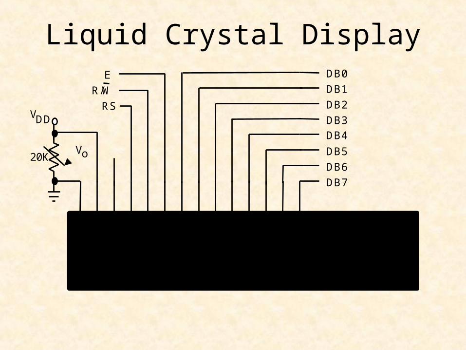
Liquid Crystal Display
2 3 4 5 6 7 9 10 1 8 11 12 13 14
16 x 1 Liquid Crystal Display
E R/W
RS V DD
V o 20K
DB0 DB1 DB2 DB3 DB4 DB5 DB6 DB7
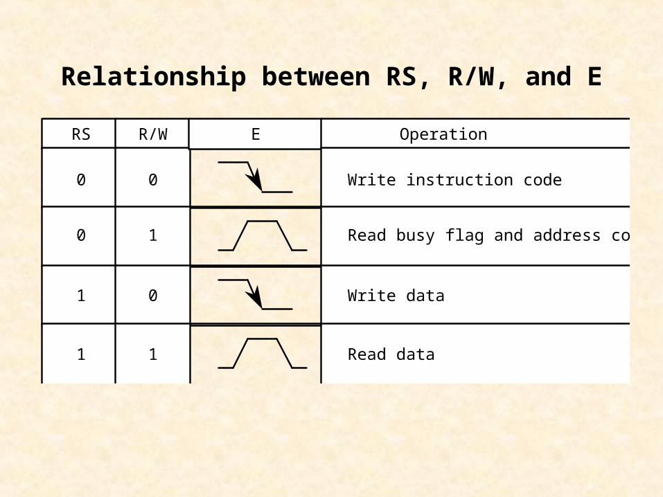
RS R/W E
0 0
0 1
1 0
1
Operation
Write instruction code
Read busy flag and address counter
Write data
Read data1
Relationship between RS, R/W, and E

Table 7.4 HD44780 Instruction SetInstruction DB7 DB6 DB5 DB4 DB3 DB2 DB1 DB0 Description
Clear display 0 0 0 0 0 0 0 1 Clears display & returns cursor to home.Sets I/D=1 in Entry Mode.
Return home 0 0 0 0 0 0 1 x Returns cursor to home position (Address 0)Set DD RAM address to zero.
Entry mode set 0 0 0 0 0 1 I/D S I/D=1: increment cursor; S=0: normal ;I/D=0: decrement cursor; S=1 shift display.
Display ON/OFFcontrol
0 0 0 0 1 D C B Sets ON/OFF all display (D), cursor (C),and blink of cursor (B).
Cursor or displayshift
0 0 0 1 S/C R/L x x S/C=1: display shift; S/C=0: cursor move;R/L=1: shift right; R/L=0: shift left.
Function set 0 0 1 DL N F x x DL=1: 8 bits; DL=0: 4 bits; N=1: 2 line;N=0: 1 line; F=1: 5x10 dots; F=0; 5x7 dots.
Set the CG RAMaddress
0 1 CG RAM address Sets the CG RAM address, after whichCG RAM data is sent and received.
Set the DD RAMaddress
1 DD RAM address Sets the DD RAM address, after whichDD RAM data is sent and received.
Read busy flag &address
BF Address counter Read busy flag (BF) and address countercontents.
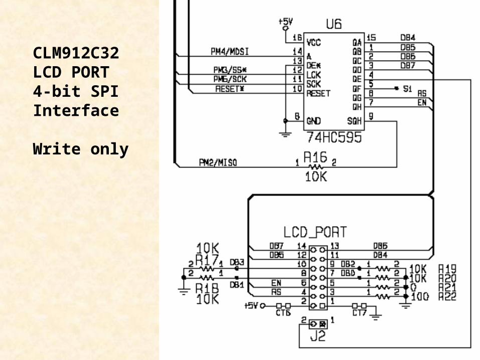
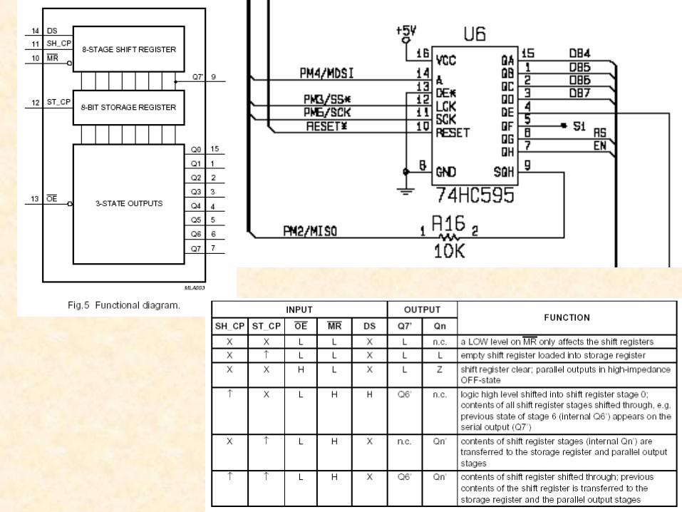
CLM912C32LCD PORT4-bit SPIInterface
Write only
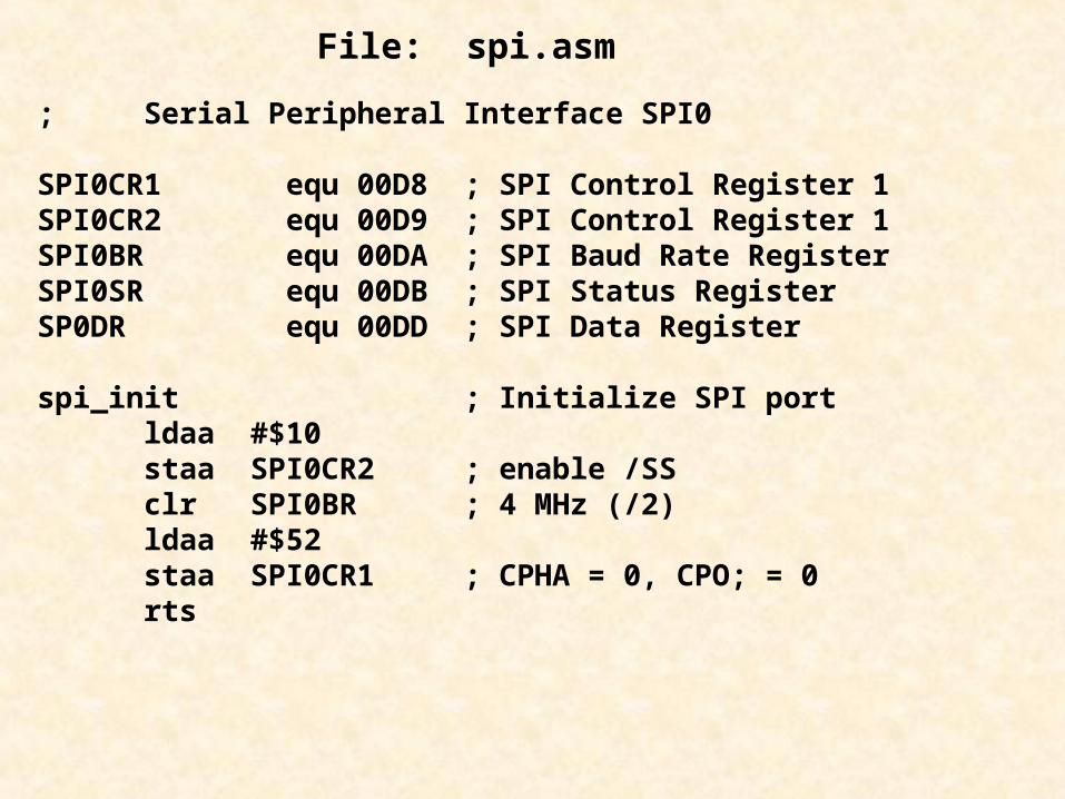
File: spi.asm
; Serial Peripheral Interface SPI0
SPI0CR1 equ 00D8 ; SPI Control Register 1SPI0CR2 equ 00D9 ; SPI Control Register 1SPI0BR equ 00DA ; SPI Baud Rate Register SPI0SR equ 00DB ; SPI Status Register SP0DR equ 00DD ; SPI Data Register spi_init ; Initialize SPI port
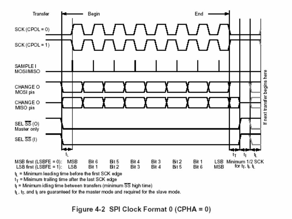
ldaa #$10staa SPI0CR2 ; enable /SSclr SPI0BR ; 4 MHz (/2)ldaa #$52staa SPI0CR1 ; CPHA = 0, CPO; = 0rts
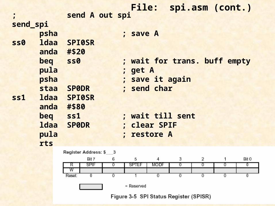
; send A out spi send_spi
psha ; save Ass0 ldaa SPI0SR
anda #$20beq ss0 ; wait for trans. buff emptypula ; get Apsha ; save it again staa SP0DR ; send char
ss1 ldaa SPI0SRanda #$80beq ss1 ; wait till sentldaa SP0DR ; clear SPIFpula ; restore Arts
File: spi.asm (cont.)
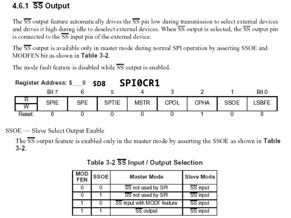
$D8 SPI0CR1
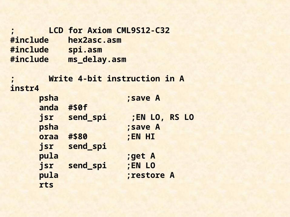
; LCD for Axiom CML9S12-C32#include hex2asc.asm#include spi.asm#include ms_delay.asm ; Write 4-bit instruction in Ainstr4
psha ;save Aanda #$0fjsr send_spi ;EN LO, RS LOpsha ;save Aoraa #$80 ;EN HIjsr send_spipula ;get Ajsr send_spi ;EN LOpula ;restore Arts
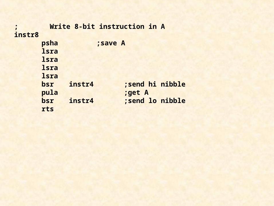
; Write 8-bit instruction in Ainstr8
psha ;save Alsralsralsralsrabsr instr4 ;send hi nibblepula ;get Absr instr4 ;send lo nibblerts
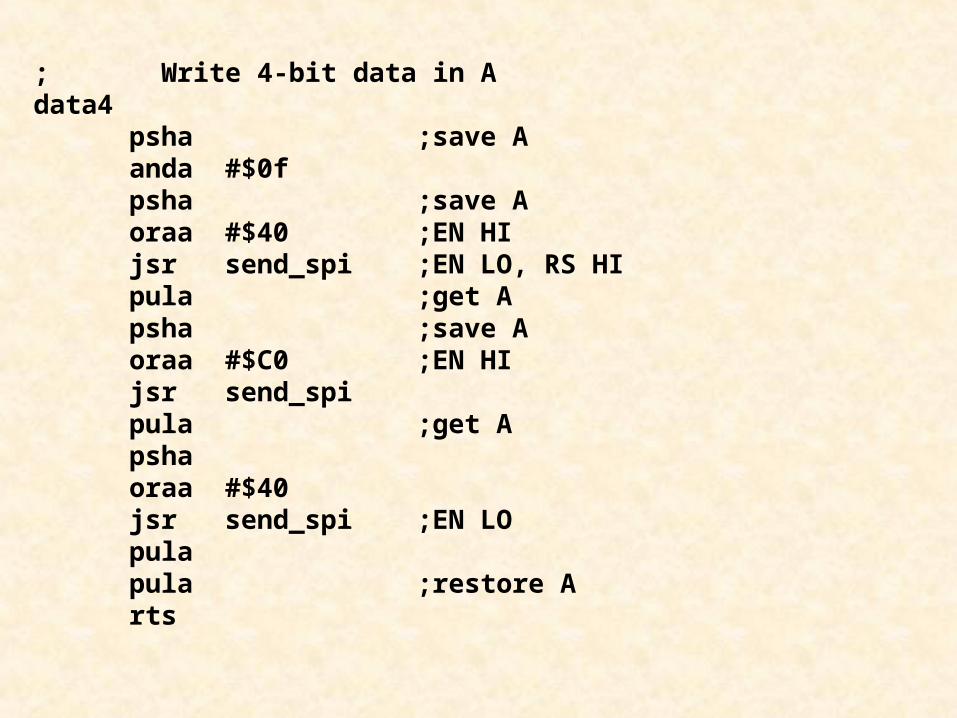
; Write 4-bit data in Adata4
psha ;save Aanda #$0fpsha ;save Aoraa #$40 ;EN HIjsr send_spi ;EN LO, RS HIpula ;get Apsha ;save Aoraa #$C0 ;EN HIjsr send_spipula ;get Apshaoraa #$40jsr send_spi ;EN LOpulapula ;restore Arts
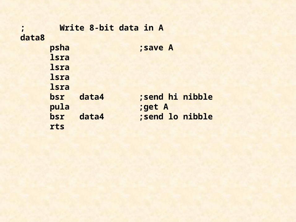
; Write 8-bit data in Adata8
psha ;save Alsralsralsralsrabsr data4 ;send hi nibblepula ;get Absr data4 ;send lo nibblerts
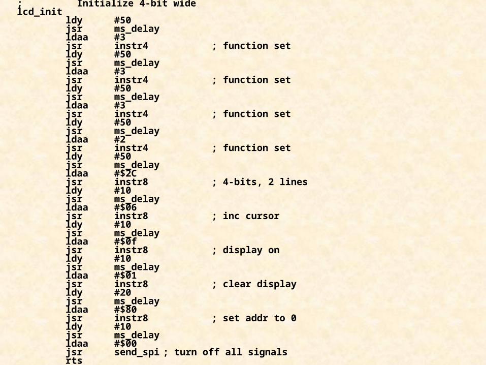
; Initialize 4-bit widelcd_init
ldy #50jsr ms_delayldaa #3jsr instr4 ; function setldy #50jsr ms_delayldaa #3jsr instr4 ; function setldy #50jsr ms_delayldaa #3jsr instr4 ; function setldy #50jsr ms_delayldaa #2jsr instr4 ; function setldy #50jsr ms_delayldaa #$2Cjsr instr8 ; 4-bits, 2 linesldy #10jsr ms_delayldaa #$06jsr instr8 ; inc cursorldy #10jsr ms_delayldaa #$0fjsr instr8 ; display onldy #10jsr ms_delayldaa #$01jsr instr8 ; clear displayldy #20jsr ms_delayldaa #$80jsr instr8 ; set addr to 0ldy #10jsr ms_delayldaa #$00jsr send_spi ; turn off all signalsrts
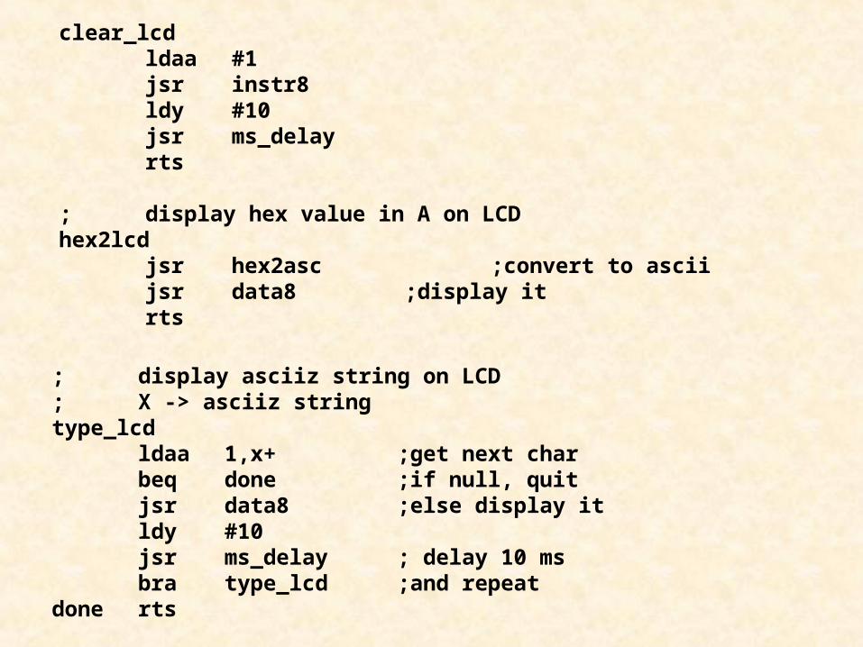
clear_lcd ldaa #1jsr instr8ldy #10jsr ms_delayrts
; display hex value in A on LCD hex2lcd
jsr hex2asc ;convert to asciijsr data8 ;display itrts
; display asciiz string on LCD; X -> asciiz string type_lcd
ldaa 1,x+ ;get next charbeq done ;if null, quitjsr data8 ;else display itldy #10jsr ms_delay ; delay 10 msbra type_lcd ;and repeat
done rts
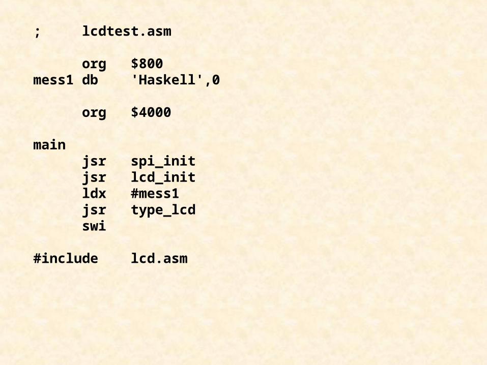
; lcdtest.asm
org $800mess1 db 'Haskell',0
org $4000
mainjsr spi_initjsr lcd_initldx #mess1jsr type_lcdswi
#include lcd.asm
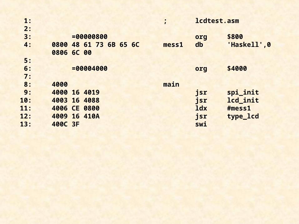
1: ; lcdtest.asm 2: 3: =00000800 org $800 4: 0800 48 61 73 6B 65 6C mess1 db 'Haskell',0 0806 6C 00 5: 6: =00004000 org $4000 7: 8: 4000 main 9: 4000 16 4019 jsr spi_init 10: 4003 16 4088 jsr lcd_init 11: 4006 CE 0800 ldx #mess1 12: 4009 16 410A jsr type_lcd 13: 400C 3F swi
74165
1
2
3
4
5
6
7
8 9
10
11
12
13
14
15
16
GND
VccSH/LD
CLK
E
F
G
Q
H
H
CLK INH
D
C
B
A
SER
QH
74165
1
2
3
4
5
6
7
8 9
10
11
12
13
14
15
16
GND
VccSH/LD
CLK
E
F
G
Q
H
H
CLK INH
D
C
B
A
SER
QH
+5V
3.3K
+5V+5V
3.3K3.3K
3.3K
+5V
0
1
2
3
4
5
6
7
8
9
A
B
C
D
E
F
MISO
SCK SS
16 x 1Hex Keypad
74165
1
2
3
4
5
6
7
8 9
10
11
12
13
14
15
16
GND
VccSH/LD
CLK
E
F
G
Q
H
H
CLK INH
D
C
B
A
SER
QH
74165
1
2
3
4
5
6
7
8 9
10
11
12
13
14
15
16
GND
VccSH/LD
CLK
E
F
G
Q
H
H
CLK INH
D
C
B
A
SER
QH
+5V
3.3K
+5V+5V
3.3K3.3K
3.3K
+5V
0
1
2
3
4
5
6
7
8
9
A
B
C
D
E
F
MISO
SCK SS
0 1 2 3 4 5 6 7 8 9 10 11 12 12 14 153 2 1 0 8 9 A B 7 6 5 4 C D E F