the sfra: a fixed frequency fpga architecturenweaver/papers/nweaver_thesis.pdf · 1 abstract the...
TRANSCRIPT

The SFRA: A Fixed Frequency FPGA Architecture
by
Nicholas Croyle Weaver
B.A. (University of California at Berkeley) 1995
A dissertation submitted in partial satisfaction of the
requirements for the degree of
Doctor of Philosophy
in
Computer Science
in the
GRADUATE DIVISION
of the
UNIVERSITY of CALIFORNIA at BERKELEY
Committee in charge:
Professor John Wawrzynek, ChairProfessor John KubiatowiczProfessor Steven Brenner
2003
The dissertation of Nicholas Croyle Weaver is approved:
Chair Date
Date
Date
University of California at Berkeley
2003

The SFRA: A Fixed Frequency FPGA Architecture
Copyright 2003
by
Nicholas Croyle Weaver
1
Abstract
The SFRA: A Fixed Frequency FPGA Architecture
by
Nicholas Croyle Weaver
Doctor of Philosophy in Computer Science
University of California at Berkeley
Professor John Wawrzynek, Chair
Field Programmable Gate Arrays (FPGAs) are synchronous digital devices used to realize digital
designs on a programmable fabric. Conventional FPGAs use design dependent clocking, so the
resulting clock frequency is dependent on the user design and the mapping process.
An alternative approach, a Fixed-Frequency FPGA, has an intrinsic clock rate at which
all designs will operate after automatic or manual modification. Fixed-Frequency FPGAs offer
significant advantages in computational throughput, throughput per unit area, and ease of integration
as a computational coprocessor in a system on a chip. Previous Fixed-Frequency FPGAs either
suffered from restrictive interconnects, application restrictions, or issues arising from the need for
new toolflows.
This thesis proposes a new interconnect topology, a “Corner Turn” network, which main-
tains the placement properties and upstream toolflows of a conventional FPGA while allowing effi-
cient, pipelined, fixed frequency operation. Global routing for this topology uses efficient, polyno-
mial time heuristics and complete searches. Detailed routing uses channel-independent packing.
C-slow retiming, a process of increasing the throughput by interleaving independent streams
of execution, is used to automatically modify designs so they operate at the array’s intrinsic clock
frequency. An additional C-slowing tool improves designs targeting conventional FPGAs to isolate
the benefits of this transformation from those arising from fixed frequency operation. This seman-
tic transformation can even be applied to a microprocessor, automatically creating an interleaved
multithreaded architecture.
Since the Corner Turn topology maintains conventional placement properties, this thesis
defines a Fixed-Frequency FPGA architecture which is placement and tool compatible with Xil-

2
inx Virtex FPGAs. By defining the architecture, estimating the area and performance cost, and
providing routing and retiming tools, this thesis directly compares the costs and benefits of a Fixed-
Frequency FPGA with a commercial FPGA.
Professor John WawrzynekDissertation Committee Chair

iii
To my grandparents, who made this all possible.

iv
Contents
List of Figures ix
List of Tables xiii
1 Introduction 11.1 What are FPGAs? . . . . . . . . . . . . . . . . . . . . . . . . . . . . . . . . . . .21.2 Why FPGAs as Computational Devices? . . . . . . . . . . . . . . . . . . . . . . .41.3 Why Fixed-Frequency FPGAs? . . . . . . . . . . . . . . . . . . . . . . . . . . . .51.4 Why the SFRA? . . . . . . . . . . . . . . . . . . . . . . . . . . . . . . . . . . . . 7
1.4.1 Why a Corner-Turn Interconnect? . . . . . . . . . . . . . . . . . . . . . .71.4.2 WhyC-slow Retiming? . . . . . . . . . . . . . . . . . . . . . . . . . . . 91.4.3 The Complete Research Toolflow . . . . . . . . . . . . . . . . . . . . . .101.4.4 This Work’s Contributions . . . . . . . . . . . . . . . . . . . . . . . . . .11
1.5 Overview of Thesis . . . . . . . . . . . . . . . . . . . . . . . . . . . . . . . . . .12
2 Related Work 142.1 FPGAs . . . . . . . . . . . . . . . . . . . . . . . . . . . . . . . . . . . . . . . . .14
2.1.1 Unpipelined interconnect, variable frequency . . . . . . . . . . . . . . . .152.1.2 Unpipelined Interconnect Studies . . . . . . . . . . . . . . . . . . . . . .182.1.3 Pipelined Interconnect, Variable Frequency . . . . . . . . . . . . . . . . .192.1.4 Pipelined, fixed frequency . . . . . . . . . . . . . . . . . . . . . . . . . .20
2.2 FPGA Tools . . . . . . . . . . . . . . . . . . . . . . . . . . . . . . . . . . . . . .212.2.1 General Placement . . . . . . . . . . . . . . . . . . . . . . . . . . . . . .212.2.2 Datapath Placement . . . . . . . . . . . . . . . . . . . . . . . . . . . . .222.2.3 Routing . . . . . . . . . . . . . . . . . . . . . . . . . . . . . . . . . . . .232.2.4 Retiming . . . . . . . . . . . . . . . . . . . . . . . . . . . . . . . . . . .23
3 Benchmarks 253.1 AES Encryption . . . . . . . . . . . . . . . . . . . . . . . . . . . . . . . . . . . .253.2 Smith Waterman . . . . . . . . . . . . . . . . . . . . . . . . . . . . . . . . . . .273.3 Synthetic microprocessor datapath . . . . . . . . . . . . . . . . . . . . . . . . . .293.4 LEON Synthesized SPARC core . . . . . . . . . . . . . . . . . . . . . . . . . . .303.5 Summary . . . . . . . . . . . . . . . . . . . . . . . . . . . . . . . . . . . . . . .31
v
I The SFRA Architecture 32
4 The Corner-Turn FPGA Topology 344.1 The Corner-Turn Interconnect . . . . . . . . . . . . . . . . . . . . . . . . . . . .344.2 Summary . . . . . . . . . . . . . . . . . . . . . . . . . . . . . . . . . . . . . . .38
5 The SFRA: A Pipelined, Corner-Turn FPGA 395.1 The SFRA Architecture . . . . . . . . . . . . . . . . . . . . . . . . . . . . . . . .395.2 The SFRA Toolflow . . . . . . . . . . . . . . . . . . . . . . . . . . . . . . . . . .435.3 Summary . . . . . . . . . . . . . . . . . . . . . . . . . . . . . . . . . . . . . . .44
6 Retiming Registers 456.1 Input Retiming . . . . . . . . . . . . . . . . . . . . . . . . . . . . . . . . . . . .456.2 Output Retiming . . . . . . . . . . . . . . . . . . . . . . . . . . . . . . . . . . .466.3 Mixed Retiming . . . . . . . . . . . . . . . . . . . . . . . . . . . . . . . . . . . .486.4 Deterministic Routing Delays . . . . . . . . . . . . . . . . . . . . . . . . . . . . .486.5 Area Costs . . . . . . . . . . . . . . . . . . . . . . . . . . . . . . . . . . . . . . .506.6 Retiming and the SFRA . . . . . . . . . . . . . . . . . . . . . . . . . . . . . . . .516.7 Summary . . . . . . . . . . . . . . . . . . . . . . . . . . . . . . . . . . . . . . .51
7 The Layout of the SFRA 527.1 Layout Strategy . . . . . . . . . . . . . . . . . . . . . . . . . . . . . . . . . . . .52
7.1.1 SRAM Cell . . . . . . . . . . . . . . . . . . . . . . . . . . . . . . . . . .557.1.2 Output Buffers . . . . . . . . . . . . . . . . . . . . . . . . . . . . . . . .577.1.3 Input Buffers . . . . . . . . . . . . . . . . . . . . . . . . . . . . . . . . .587.1.4 Interconnect Buffers . . . . . . . . . . . . . . . . . . . . . . . . . . . . .59
7.2 Overall Area . . . . . . . . . . . . . . . . . . . . . . . . . . . . . . . . . . . . . .607.3 Timing Results . . . . . . . . . . . . . . . . . . . . . . . . . . . . . . . . . . . .617.4 Summary . . . . . . . . . . . . . . . . . . . . . . . . . . . . . . . . . . . . . . .61
8 Routing a Corner-Turn Interconnect 638.1 Interaction with Retiming . . . . . . . . . . . . . . . . . . . . . . . . . . . . . . .648.2 The Routing Process . . . . . . . . . . . . . . . . . . . . . . . . . . . . . . . . .64
8.2.1 Direct Routing . . . . . . . . . . . . . . . . . . . . . . . . . . . . . . . .658.2.2 Fanout Routing . . . . . . . . . . . . . . . . . . . . . . . . . . . . . . . .658.2.3 Pushrouting . . . . . . . . . . . . . . . . . . . . . . . . . . . . . . . . . .668.2.4 Zig-zag (2 turn) routing . . . . . . . . . . . . . . . . . . . . . . . . . . .678.2.5 Randomized Ripup and Reroute . . . . . . . . . . . . . . . . . . . . . . .688.2.6 Detailed Routing . . . . . . . . . . . . . . . . . . . . . . . . . . . . . . .68
8.3 Routing Quality & Analysis . . . . . . . . . . . . . . . . . . . . . . . . . . . . .698.3.1 AES . . . . . . . . . . . . . . . . . . . . . . . . . . . . . . . . . . . . . .698.3.2 Smith/Waterman . . . . . . . . . . . . . . . . . . . . . . . . . . . . . . .718.3.3 Synthetic Microprocessor Datapath . . . . . . . . . . . . . . . . . . . . .728.3.4 Leon 1 . . . . . . . . . . . . . . . . . . . . . . . . . . . . . . . . . . . .74
8.4 Summary . . . . . . . . . . . . . . . . . . . . . . . . . . . . . . . . . . . . . . .75

vi
9 Other Implications of the Corner-Turn Interconnect 769.1 Defect Tolerance . . . . . . . . . . . . . . . . . . . . . . . . . . . . . . . . . . .769.2 Memory Blocks . . . . . . . . . . . . . . . . . . . . . . . . . . . . . . . . . . . .789.3 Hardware Assisted Routing . . . . . . . . . . . . . . . . . . . . . . . . . . . . . .799.4 Heterogeneous channels . . . . . . . . . . . . . . . . . . . . . . . . . . . . . . .809.5 Summary . . . . . . . . . . . . . . . . . . . . . . . . . . . . . . . . . . . . . . .80
II Retiming 81
10 Retiming, C-slow Retiming, and Repipelining 8310.1 Retiming . . . . . . . . . . . . . . . . . . . . . . . . . . . . . . . . . . . . . . .8410.2 Repipelining . . . . . . . . . . . . . . . . . . . . . . . . . . . . . . . . . . . . . .8710.3 C-slow Retiming . . . . . . . . . . . . . . . . . . . . . . . . . . . . . . . . . . .8810.4 Retiming for Conventional FPGAs . . . . . . . . . . . . . . . . . . . . . . . . . .9010.5 Retiming for Fixed Frequency FPGAs . . . . . . . . . . . . . . . . . . . . . . . .9110.6 Previous Retiming Tools . . . . . . . . . . . . . . . . . . . . . . . . . . . . . . .9310.7 Summary . . . . . . . . . . . . . . . . . . . . . . . . . . . . . . . . . . . . . . .94
11 Applying C-Slow Retiming to Microprocessor Architectures 9511.1 Introduction . . . . . . . . . . . . . . . . . . . . . . . . . . . . . . . . . . . . . .9511.2 C-slowing a Microprocessor . . . . . . . . . . . . . . . . . . . . . . . . . . . . .96
11.2.1 Register File . . . . . . . . . . . . . . . . . . . . . . . . . . . . . . . . .9811.2.2 TLB . . . . . . . . . . . . . . . . . . . . . . . . . . . . . . . . . . . . . .9911.2.3 Caches and Memory . . . . . . . . . . . . . . . . . . . . . . . . . . . . .9911.2.4 Branch Prediction . . . . . . . . . . . . . . . . . . . . . . . . . . . . . . .10011.2.5 Control Registers and Machine State . . . . . . . . . . . . . . . . . . . . .10011.2.6 Interrupts . . . . . . . . . . . . . . . . . . . . . . . . . . . . . . . . . . .10111.2.7 Interthread Synchronization . . . . . . . . . . . . . . . . . . . . . . . . .10111.2.8 Power Consumption . . . . . . . . . . . . . . . . . . . . . . . . . . . . .101
11.3 C-slowing LEON . . . . . . . . . . . . . . . . . . . . . . . . . . . . . . . . . . .10211.4 Summary . . . . . . . . . . . . . . . . . . . . . . . . . . . . . . . . . . . . . . .103
12 The Effects of Placement and Hand C-slowing 10412.1 The Effects of Hand Placement andC-slow Retiming . . . . . . . . . . . . . . . .10412.2 AES Results . . . . . . . . . . . . . . . . . . . . . . . . . . . . . . . . . . . . . .10612.3 Smith/Waterman results . . . . . . . . . . . . . . . . . . . . . . . . . . . . . . . .10712.4 Synthetic Datapath Results . . . . . . . . . . . . . . . . . . . . . . . . . . . . . .10812.5 Summary . . . . . . . . . . . . . . . . . . . . . . . . . . . . . . . . . . . . . . .109
13 Automatically Applying C-Slow Retiming to Xilinx FPGAs 11013.1 Retiming and the Xilinx Toolflow . . . . . . . . . . . . . . . . . . . . . . . . . .11013.2 An Automated C-Slow Tool for Virtex FPGAs . . . . . . . . . . . . . . . . . . . .11213.3 Results . . . . . . . . . . . . . . . . . . . . . . . . . . . . . . . . . . . . . . . . .115
13.3.1 AES Encryption . . . . . . . . . . . . . . . . . . . . . . . . . . . . . . .116

vii
13.3.2 Smith/Waterman . . . . . . . . . . . . . . . . . . . . . . . . . . . . . . .11813.3.3 Synthetic Datapath . . . . . . . . . . . . . . . . . . . . . . . . . . . . . .12013.3.4 LEON 1 . . . . . . . . . . . . . . . . . . . . . . . . . . . . . . . . . . . .120
13.4 Architectural Recommendations for the Xilinx . . . . . . . . . . . . . . . . . . . .12113.5 Retiming for the SFRA . . . . . . . . . . . . . . . . . . . . . . . . . . . . . . . .12113.6 Summary . . . . . . . . . . . . . . . . . . . . . . . . . . . . . . . . . . . . . . .122
III Comparisons, Reflections and Conclusions 123
14 Comparing the SFRA with the Xilinx Virtex 12514.1 Benchmark Designs . . . . . . . . . . . . . . . . . . . . . . . . . . . . . . . . . .12514.2 The SFRA Target . . . . . . . . . . . . . . . . . . . . . . . . . . . . . . . . . . .12614.3 The Xilinx Target . . . . . . . . . . . . . . . . . . . . . . . . . . . . . . . . . . .12614.4 Toolflow Comparisons . . . . . . . . . . . . . . . . . . . . . . . . . . . . . . . .12714.5 Throughput Comparisons withoutC-slowing . . . . . . . . . . . . . . . . . . . . 12914.6 Throughput Comparisons withC-slowing . . . . . . . . . . . . . . . . . . . . . .13114.7 Latency Comparisons . . . . . . . . . . . . . . . . . . . . . . . . . . . . . . . . .13214.8 Summary . . . . . . . . . . . . . . . . . . . . . . . . . . . . . . . . . . . . . . .133
15 Latency and Throughput: Is Fixed-Frequency a Superior Approach? 13415.1 The Limits of Parallelism . . . . . . . . . . . . . . . . . . . . . . . . . . . . . . .13515.2 Latency and Cryptography . . . . . . . . . . . . . . . . . . . . . . . . . . . . . .13615.3 Latency and Fixed-Frequency FPGAs . . . . . . . . . . . . . . . . . . . . . . . .13715.4 Pseudo-Fixed-Frequency FPGA tools . . . . . . . . . . . . . . . . . . . . . . . .13815.5 Recommendations & Conclusions . . . . . . . . . . . . . . . . . . . . . . . . . .139
16 Open Questions 14116.1 Power Consumption andC-slowing . . . . . . . . . . . . . . . . . . . . . . . . .14116.2 Corner-Turn Interconnect and Coarse-Grained FPGAs . . . . . . . . . . . . . . .14316.3 Depopulated C-boxes . . . . . . . . . . . . . . . . . . . . . . . . . . . . . . . . .14316.4 Summary . . . . . . . . . . . . . . . . . . . . . . . . . . . . . . . . . . . . . . .144
17 Conclusion 14517.1 Benchmark Selection . . . . . . . . . . . . . . . . . . . . . . . . . . . . . . . . .14617.2 The SFRA . . . . . . . . . . . . . . . . . . . . . . . . . . . . . . . . . . . . . . .147
17.2.1 Corner Turn Interconnect and Fast Routing . . . . . . . . . . . . . . . . .14717.2.2 Compatibility . . . . . . . . . . . . . . . . . . . . . . . . . . . . . . . . .14717.2.3 Fixed Frequency Operation . . . . . . . . . . . . . . . . . . . . . . . . . .148
17.3 C-slowing and Retiming . . . . . . . . . . . . . . . . . . . . . . . . . . . . . . .14917.4 Applications to Commercial Products . . . . . . . . . . . . . . . . . . . . . . . .150
Bibliography 152
viii
A Case Study: AES Encryption 160A.1 Introduction . . . . . . . . . . . . . . . . . . . . . . . . . . . . . . . . . . . . . .161A.2 The AES Encryption Algorithm . . . . . . . . . . . . . . . . . . . . . . . . . . .162A.3 Modes of Operation . . . . . . . . . . . . . . . . . . . . . . . . . . . . . . . . . .163A.4 Implementing Block Ciphers in Hardware . . . . . . . . . . . . . . . . . . . . . .164A.5 Implementing AES in Hardware . . . . . . . . . . . . . . . . . . . . . . . . . . .166A.6 AES Subkey Generation . . . . . . . . . . . . . . . . . . . . . . . . . . . . . . .167A.7 AES Encryption Core . . . . . . . . . . . . . . . . . . . . . . . . . . . . . . . . .168A.8 Testing . . . . . . . . . . . . . . . . . . . . . . . . . . . . . . . . . . . . . . . . .169A.9 Performance . . . . . . . . . . . . . . . . . . . . . . . . . . . . . . . . . . . . . .170A.10 Other implementations . . . . . . . . . . . . . . . . . . . . . . . . . . . . . . . .170A.11 Reflections . . . . . . . . . . . . . . . . . . . . . . . . . . . . . . . . . . . . . .172A.12 Summary . . . . . . . . . . . . . . . . . . . . . . . . . . . . . . . . . . . . . . .173
B Other Multithreaded Architectures 174B.1 Previous Multithreaded Architectures . . . . . . . . . . . . . . . . . . . . . . . .174B.2 Synergistic and interference effects . . . . . . . . . . . . . . . . . . . . . . . . . .176

ix
List of Figures
1.1 (A) A simplified FPGA Logic Element (LE) consisting of two 4-input lookup tables(4-LUTs), dedicated arithmetic logic, and 2 flip-flops and (B) The classical compo-nents of a Manhattan FPGA: the LE (logic element) performs the computation, theC-box (connection box) connects the LE to the interconnect, and the S-box (switchbox) provides for connections within the interconnect. . . . . . . . . . . . . . . . .2
1.2 A typical FPGA CAD flow. User designs are entered either as schematics or in ahigh level description language (HDL). These designs are firstsynthesizedto createa netlist, which is thenmappedonto the FPGA logic elements. These elements arethenplacedon the array, the connections between the elements arerouted, and thefinal design undergoestiming analysis . . . . . . . . . . . . . . . . . . . . . . . . 3
1.3 (A) A crossbar switch-box. (B) A physically-depopulated crossbar. (C) A capacity-depopulated crossbar. . . . . . . . . . . . . . . . . . . . . . . . . . . . . . . . . .8
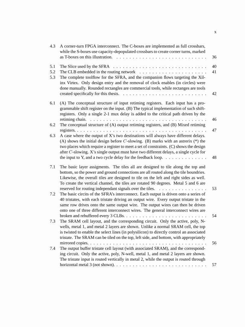
1.4 A corner-turn FPGA interconnect. The C-boxes are implemented as full crossbars,while the S-boxes use capacity-depopulated crossbars to create corner turns, markedas T-boxes on this illustration. . . . . . . . . . . . . . . . . . . . . . . . . . . . .8
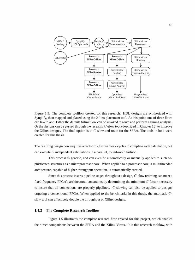
1.5 The complete toolflow created for this research. HDL designs are synthesized withSynplify, then mapped and placed using the Xilinx placement tool. At this point,one of three flows can take place. Either the default Xilinx flow can be invokedto route and perform a timing analysis. Or the designs can be passed through theresearchC-slow tool (described in Chapter 13) to improve the Xilinx designs. Thefinal option is toC-slow and route for the SFRA. The tools in bold were created forthis thesis. . . . . . . . . . . . . . . . . . . . . . . . . . . . . . . . . . . . . . .10
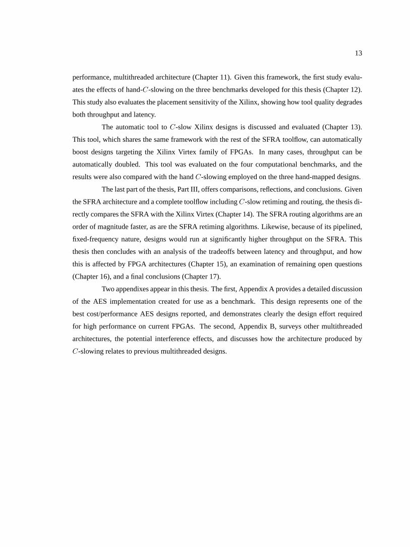
2.1 A Virtex CLB, and the details of a single CLB-slice, from the Xilinx Datasheet [82].152.2 The Stratix Logic Element (LE), from the Stratix datasheet[4] . . . . . . . . . . .17
3.1 Layout of an individual systolic cell for the Smith/Waterman sequence matchingcomputation . . . . . . . . . . . . . . . . . . . . . . . . . . . . . . . . . . . . . .27
4.1 The classical components of a Manhattan FPGA: the LE (logic element) performsthe computation, the C-box (connection box) connects the LE to the interconnect,and the S-box (switch box) provides for connections within the interconnect. . . . .34
4.2 (A) A crossbar switch-box. (B) A physically depopulated crossbar. (C) A capacity-depopulated crossbar. . . . . . . . . . . . . . . . . . . . . . . . . . . . . . . . . .35
x
4.3 A corner-turn FPGA interconnect. The C-boxes are implemented as full crossbars,while the S-boxes use capacity-depopulated crossbars to create corner turns, markedas T-boxes on this illustration. . . . . . . . . . . . . . . . . . . . . . . . . . . . .36
5.1 The Slice used by the SFRA . . . . . . . . . . . . . . . . . . . . . . . . . . . . .405.2 The CLB embedded in the routing network . . . . . . . . . . . . . . . . . . . . .415.3 The complete toolflow for the SFRA, and the companion flows targeting the Xil-
inx Virtex. Only design entry and the removal of clock enables (in circles) weredone manually. Rounded rectangles are commercial tools, while rectanges are toolscreated specifically for this thesis. . . . . . . . . . . . . . . . . . . . . . . . . . .42
6.1 (A) The conceptual structure of input retiming registers. Each input has a pro-grammable shift register on the input. (B) The typical implementation of such shift-registers. Only a single 2-1 mux delay is added to the critical path driven by theretiming chain. . . . . . . . . . . . . . . . . . . . . . . . . . . . . . . . . . . . .46
6.2 The conceptual structure of (A) output retiming registers, and (B) Mixed retimingregisters. . . . . . . . . . . . . . . . . . . . . . . . . . . . . . . . . . . . . . . . .47
6.3 A case where the output of X’s two destinations will always have different delays.(A) shows the initial design beforeC-slowing. (B) marks with an astrerix (*) thetwo places which require a register to meet a set of constraints. (C) shows the designafterC-slowing. X’s single output must have two different delays, a single cycle forthe input to Y, and a two cycle delay for the feedback loop. . . . . . . . . . . . . .48
7.1 The basic layer assigments. The tiles all are designed to tile along the top andbottom, so the power and ground connections are all routed along the tile boundries.Likewise, the overall tiles are designed to tile on the left and right sides as well.To create the vertical channel, the tiles are rotated 90 degrees. Metal 5 and 6 arereserved for routing independant signals over the tiles. . . . . . . . . . . . . . . .53
7.2 The basic circits of the SFRA’s interconnect. Each output is driven onto a series of40 tristates, with each tristate driving an output wire. Every output tristate in thesame row drives onto the same output wire. The output wires can then be drivenonto one of three different interconnect wires. The general interconnect wires arebroken and rebuffered every 3 CLBs. . . . . . . . . . . . . . . . . . . . . . . . . .54
7.3 The SRAM cell layout, and the corresponding circuit. Only the active, poly, N-wells, metal 1, and metal 2 layers are shown. Unlike a normal SRAM cell, the topis twisted to enable the select lines (in polysilicon) to directly control an associatedtristate. The SRAM can be tiled on the top, left side, and bottom, with appropriatelymirrored copies. . . . . . . . . . . . . . . . . . . . . . . . . . . . . . . . . . . . .56
7.4 The output buffer tristate cell layout (with associated SRAM), and the correspond-ing circuit. Only the active, poly, N-well, metal 1, and metal 2 layers are shown.The tristate input is routed vertically in metal 2, while the output is routed throughhorizontal metal 3 (not shown). . . . . . . . . . . . . . . . . . . . . . . . . . . . .57
xi
7.5 The input buffer’s tristate layout. Only the active, poly, N-wells, metal 1, and metal2 layers are shown. The left side contains three tristates. The inputs arrive horizon-tally in metal 3 (not shown) and the outputs are processed vertically in metal 2. Theother metal 2 connections are from the other group of tristates for the same input. .58
7.6 The interconnect buffer layout with associated SRAM cell, and the correspondingcircuit implemented. Only the active, poly, N-wells, metal 1, and metal 2 layers areshown. Both input and output occur on either metal 3 or metal 4, with the inputdriving the small inverter used to drives the large tristate. . . . . . . . . . . . . . .59
7.7 The SFRA’s CLB tile, and the comparative size of the Xilinx Virtex-E tile and ascaled HSRA tile containing 4 LUTs. The portions of the SFRA’s tile shown in graywere layed out to determine the critical area and path of the design. The HSRA tileis based on an area of approximately 4 Mλ2 per LUT, scaled to a .18µm process. . 60
8.1 The two options considered by fanout routing, (A): starting horizontally and branch-ing vertically and (B), starting vertically and branching horizontally. . . . . . . . .65
8.2 (A): The two possible single-turn routes. (B): An initial configuration before pushrout-ing the connection between the gray boxes. (C): The configuration after pushrout-ing. In this example, each switchpoint supports only a single turn. . . . . . . . . .66
8.3 (A) The possible zig-zag routes which start horizontally and (B) The possible zig-zag routes which start vertically. . . . . . . . . . . . . . . . . . . . . . . . . . . .68
9.1 (A) The gray signal is affected by the interconnect break marked with an X. (B) Thegray signal is now rerouted to avoid the break. . . . . . . . . . . . . . . . . . . . .77
9.2 (A) The gray signal is affected by the stuck-on interconnect point marked with anX. (B) The gray signal is now rerouted to use the stuck-on point. . . . . . . . . . .77
10.1 (A): A small graph before retiming. The nodes represent logic delays, with theinputs and outputs passing through mandatory, fixed registers. The critical path is5. The input and output registers can not be moved. (B): The same graph afterretiming. The critical path is reduced from 5 to 4. Yet the I/O semantics have notchanged, as it still requires three cycles for a datum to proceed from input to output.85
10.2 (A): The example from Figure 10.1 which is converted to2-slow operation. Thecritical path remains unchanged, but now the design will operate on two indepen-dant streams in a round-robin fashion. (B): The design is now retimed. By takingadvantage of the extra flip-flops, the critical path has been reduced from 5 to 2. . .89
11.1 A classic 5 stage microprocessor pipeline . . . . . . . . . . . . . . . . . . . . . .9711.2 A conceptual view of the classic 5 stage microprocessor afterC-slowing by a factor
of 3. The resulting core now is a 15 stage pipeline, and operates on 3 independentstreams in a round-robin fashion. The actual register placements will not be so even,as automatic retiming will place registers in the most appropriate positions on eachindividual path. . . . . . . . . . . . . . . . . . . . . . . . . . . . . . . . . . . . .97
13.1 The complete toolflow created for this research. This section focuses on the Xilinxretiming tool, with its comparisons to the unoptimized Xilinx designs. . . . . . . .112

xii
13.2 C-slowing and retiming all the benchmarks and the effects on throughput and la-tency. AC-slow factor of 1 just performs retiming. Throughput is substantially im-proved, roughly doubling the throughput in the best case. As expected,C-slowingdoes increase the latency for a single computation. . . . . . . . . . . . . . . . . .115
A.1 The AES round structure . . . . . . . . . . . . . . . . . . . . . . . . . . . . . . .162A.2 Three Common Operating Modes. A) Electronic Code Book (ECB), B) Cipher
Block Chaining (CBC), C) Counter (CTR) . . . . . . . . . . . . . . . . . . . . . .163A.3 The relative area performance and throughput for tiling verses tiling different levels
of unrolling verses just unrolling, for a cipher consisting of 10 repeated rounds,based on a 2.5% area savings for muxes and control logic when unrolling. . . . . .165
A.4 The Subkey Generation Implementation in a Xilinx Spartan II-100. Arrowheads arethe location of pipeline stages, dataflow shown at 16 bit granularity. . . . . . . . .167
A.5 The Encryption Core Implementation in a Xilinx Spartan II-100. Arrowheads arethe location of pipeline stages, dataflow shown at 8 bit granularity. . . . . . . . . .169
xiii
List of Tables
4.1 Comparing the costs of a full crossbar,k physically-depopulated crossbar, and atturn capacity-depopulated crossbar for ann by n channel intersection. . . . . . . . 36
8.1 Global Routing the hand-placed AES benchmark. The number of turns include theuse of 4 BX/BY inputs to implement 4 turns. . . . . . . . . . . . . . . . . . . . .70
8.2 Global Routing the automatically-placed AES benchmark. The number of turnsinclude the use of the 4 BX/BY inputs to implement 4 turns. . . . . . . . . . . . .70
8.3 Detailed Routing the hand-placed AES benchmark . . . . . . . . . . . . . . . . .708.4 Detailed Routing the automatically-placed AES benchmark . . . . . . . . . . . . .718.5 Global Routing for the hand-placed Smith/Waterman benchmark. The number of
turns include the use of BX/BY inputs. . . . . . . . . . . . . . . . . . . . . . . . .718.6 Global Routing for the automatically placed Smith/Waterman benchmark. The
number of turns include the use of BX/BY inputs. . . . . . . . . . . . . . . . . . .718.7 Detailed Routing the hand-placed Smith/Waterman benchmark. . . . . . . . . . . .728.8 Detailed Routing the automatically-placed Smith/Waterman benchmark. . . . . . .728.9 Global Routing for the hand-placed synthetic datapath. The number of turns include
the use of BX/BY inputs. . . . . . . . . . . . . . . . . . . . . . . . . . . . . . . .738.10 Global Routing for the automatically-placed synthetic datapath. The number of
turns include the use of BX/BY inputs. . . . . . . . . . . . . . . . . . . . . . . . .738.11 Detailed Routing for the hand-placed synthetic datapath . . . . . . . . . . . . . . .738.12 Detailed Routing for the automatically-placed synthetic datapath . . . . . . . . . .738.13 Global Routing for the LEON SPARC core. The number of turns include the use of
BX/BY inputs. . . . . . . . . . . . . . . . . . . . . . . . . . . . . . . . . . . . . 748.14 Detailed Routing the Leon SPARC Core. . . . . . . . . . . . . . . . . . . . . . . .74
10.1 The constraint system used by the retiming process.r(u) is the lag computed foreach node,w(e) is the initial number of registers on an edge,W (u, v) is the mini-mum number of registers betweenu andv, andD(u, v) is the critical path betweenu andv . . . . . . . . . . . . . . . . . . . . . . . . . . . . . . . . . . . . . . . . 84
10.2 The effects of various FPGA and design features on retiming andC-slow retiming . 88
11.1 Published Implementation Technologies and Performance for the LEON processorcore [54]. . . . . . . . . . . . . . . . . . . . . . . . . . . . . . . . . . . . . . . .102
11.2 The latency for various instructions in the LEON pipeline [54]. . . . . . . . . . . .103
xiv
12.1 Parameters, Clock Rate, and Place and Route (P&R) time for the AES benchmark,targeting a Spartan II 100-5. . . . . . . . . . . . . . . . . . . . . . . . . . . . . .105
12.2 Latency, Throughput, and area values for the AES benchmark, targeting a SpartanII 100-5 . . . . . . . . . . . . . . . . . . . . . . . . . . . . . . . . . . . . . . . .106
12.3 Parameters, clock rate, and place and route time for the Smith/Waterman bench-mark, 8 cells, targeting a Spartan II-200-5 . . . . . . . . . . . . . . . . . . . . . .107
12.4 Parameters, clock rate, and place and route time for the synthetic datapath, targetinga Spartan II-150-5 . . . . . . . . . . . . . . . . . . . . . . . . . . . . . . . . . . .108
13.1 The effects of C-slow retiming the AES encryption core placed with simulated an-nealing on a Spartan II 100. This tool produces highly competitive results, able tonearly double the throughput using automated transformations. . . . . . . . . . . .116
13.2 The effects of C-slow retiming the hand placed AES encryption core targeting aSpartan II 100. For 5-slow retiming, the throughput more than doubled when com-pared with the original, unretimed version. . . . . . . . . . . . . . . . . . . . . . .116
13.3 The effects of C-slow retiming on the Smith/Waterman Implementation, for simu-lated annealing placement on a Spartan II 200. The 3 slow version almost doublesthe throughput, while the automatic 4 slow version has passed the point of dimin-ishing returns due to the large number of flip flops that required allocation. . . . . .118
13.4 The effects of C-slow retiming on the Smith/Waterman Implementation for handplacement on a Spartan II 200. Again, a highC factor nearly doubles the throughput.118
13.5 The effects of C-slow retiming on the synthetic microprocessor core targeting aSpartan II 150-5, placed with simulated annealing. . . . . . . . . . . . . . . . . .119
13.6 The effects of C-slow retiming on the hand placed synthetic microprocessor datap-ath targeting a Spartan II 150-5 . . . . . . . . . . . . . . . . . . . . . . . . . . . .119
13.7 The effects of C-slow retiming on the LEON 1 SPARC microprocessor core target-ing a Virtex 400-6. The 2 slow version doubles the throughput, while maintainingroughly the same latency, while the 3 slow version allocated too many flip flops tobe effective. . . . . . . . . . . . . . . . . . . . . . . . . . . . . . . . . . . . . . .120
14.1 The initial clock rates for the various benchmarks, targeting the Spartan II/Virtexparts, and the clock rate adjusted to the .18µm process. This clock rate adjustmentis necessary because although the .18 and .25µm parts are similar, there are minorincompatibilities which restrict the automaticC-slow retiming tool. . . . . . . . . 128
14.2 Time taken by the tools to route and retime the benchmarks, for both Xilinx Virtexand the SFRA. The SFRA toolflow time includes both routing and retiming, whilethe Xilinx retiming time excludes theO(n3) Dijkstra’s step used to calculate theWandD matrixes. The SFRA router minimizes the number of turns required for eachconnection and all connections use minimum-length wires. . . . . . . . . . . . . .129
14.3 Throughput and Throughput/Area results for the unoptimized Virtex benchmarkswhen compared with an 300 MHz SFRA. . . . . . . . . . . . . . . . . . . . . . .130
14.4 Performance results for automaticallyC-slowed applications when compared withan 300 MHz SFRA. . . . . . . . . . . . . . . . . . . . . . . . . . . . . . . . . . .132
14.5 Latency results for the Virtex benchmarks when compared with a 300 MHz SFRA.133

xv
A.1 Latency, Throughput, and Area requirements for various versions of this Rijndael core161A.2 Throughput, Area, and Throughput/Area for this implementation compared with
other commercial and academic implementations on Spartan II and Virtex FPGAs.171A.3 Throughput, Area, and Throughput/Area for this implementation compared with
commercial implementations on Virtex-E FPGAs. . . . . . . . . . . . . . . . . . .171

xvi
Acknowledgements
The Corner Turning Interconnect was first proposed by John Hauser. Yury Markovskiy and Yatish
Patel provided assistance in adapting the LEON benchmark to meet the requirements for fixed-
frequency operation. Victor Wen helped with the CAD tools. Many thanks to the Berkeley Wireless
Research Center and ST Microsystems which provided access, tools, and design rules for the .18
µm process.
Elyon Caspi, Randy Huang, Joseph Yeh, and Andre DeHon all provided much valuable
advice and comments. My committee: John Wawrzynek, John Kubiatowitz, and Steven Brenner,
all provided excellent comments and assistance. My mother, Janet Weaver, also provided excellent
editing.
1
Chapter 1
Introduction
As VLSI fabrication technologies continue to advance and the number of available tran-
sistors increases, the research community continues to devote considerable effort to build scalable,
high performance computational fabrics. Such architectures offer the promise of performance which
scales linearly with silicon area without increasing the implementation complexity.
One particular class of architectures, commonly described as Field Programmable Gate
Arrays (FPGAs) [82, 4] or Reconfigurable Arrays, are of particular interest because of their scala-
bility, performance, potential for defect tolerance, and ability to map arbitrary digital designs.
Conventional FPGA’s utilize design-dependent clocking, thus the array’s clock frequency
is not an intrinsic constant but depends on the design or program being run. An alternate approach is
a fixed-frequencyFPGA, where the clock frequency is a property of the computational array rather
than the particular design currently running on the FPGA.
This thesis introduces a new FPGA architecture, the SFRA1, and the associated CAD tools
necessary to map designs to this new architecture. The SFRA runs at a significantly higher clock
rate than a conventional FPGA, and can therefore run designs at a significantly higherthroughput.
Unlike previous fixed-frequency FPGAs, the SFRA is designed to map arbitrary digital
designs and is directly compatible with a commercial FPGA, the Xilinx Virtex. Thus the SFRA can
utilize the Xilinx synthesis and placement tools and can be directly compared against a success-
ful commercial FPGA. Unlike other FPGAs, the SFRA’s interconnect enables much faster routing
algorithms, capable of routing designs in seconds rather than minutes.
1“SFRA” means either “Synchronous and Flexible Reconfigurable Array” (based on its fixed-frequency routing ar-chitecture) or “San Francisco Reconfigurable Array” (based on the numerous “No Left Turn” signs in the city of SanFrancisco).

2
LEC-Box
C-B
oxS-Box
LEC-Box
C-B
oxS-Box
LEC-Box
C-B
oxS-Box
LEC-Box
C-B
oxS-Box
LEC-Box
C-B
oxS-Box
LEC-Box
C-B
oxS-Box
LEC-Box
C-B
oxS-Box
LEC-Box
C-B
oxS-Box
(B)(A)
YQ
Y
4-LUT
Add�Logic
G4G3G2G1
XQ
X
4-LUT
Add�Logic
F4F3F2F1
CIN
COUT
Figure 1.1: (A) A simplified FPGA Logic Element (LE) consisting of two 4-input lookup tables (4-LUTs), dedicated arithmetic logic, and 2 flip-flops and (B) The classical components of a ManhattanFPGA: the LE (logic element) performs the computation, the C-box (connection box) connects theLE to the interconnect, and the S-box (switch box) provides for connections within the interconnect.
To support the fine-degree of pipelining present in the SFRA, the SFRA’s toolflow in-
cludesC-slow retiming. This transformation automatically repipelines SFRA designs to run at the
array’s intrinsic clock frequency. The tool can also be used to improve designs targeting the Xilinx
Virtex, automatically doubling their throughput in many cases.
1.1 What are FPGAs?
An FPGA, or Field Programmable Gate Array, generally consists of a small, replicated
logic element (LE) embedded in a circuit switched interconnect. These logic elements usually
consist of a group of small lookup tables (LUTs), a small amount of fixed carry-logic, and flip-
flops. Figure 1.1(A) shows a simplified LE containing two 4-LUTs, two bits of carry-logic, and two
flip-flops. This LE can be used to implement a two bit adder or two independent boolean functions
with four inputs each.
These LEs are then embedded in a larger network, as illustrated in Figure 1.1(B). The
LE is connected to connection boxes (C-boxes) which route signals onto a general-purpose, circuit
switched interconnect. Signals on the general interconnect are routed by switch boxes (S-boxes).
By configuring the LEs and interconnect, an FPGA can implement arbitrary synchronous digital
designs.
An FPGA architecture does not just consist of an FPGA design, but an associated suite of
CAD tools (also known as a toolflow) which accepts user designs and maps them to the target FPGA.
3
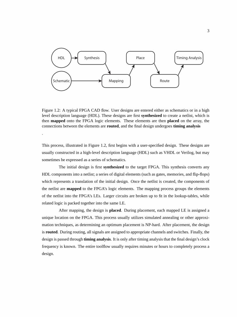
Synthesis
Mapping Route
Place Timing Analysis
Schematic
HDL
Figure 1.2: A typical FPGA CAD flow. User designs are entered either as schematics or in a highlevel description language (HDL). These designs are firstsynthesizedto create a netlist, which isthenmapped onto the FPGA logic elements. These elements are thenplaced on the array, theconnections between the elements arerouted, and the final design undergoestiming analysis
.
This process, illustrated in Figure 1.2, first begins with a user-specified design. These designs are
usually constructed in a high-level description language (HDL) such as VHDL or Verilog, but may
sometimes be expressed as a series of schematics.
The initial design is firstsynthesizedto the target FPGA. This synthesis converts any
HDL components into a netlist; a series of digital elements (such as gates, memories, and flip-flops)
which represents a translation of the initial design. Once the netlist is created, the components of
the netlist aremapped to the FPGA’s logic elements. The mapping process groups the elements
of the netlist into the FPGA’s LEs. Larger circuits are broken up to fit in the lookup-tables, while
related logic is packed together into the same LE.
After mapping, the design isplaced. During placement, each mapped LE is assigned a
unique location on the FPGA. This process usually utilizes simulated annealing or other approxi-
mation techniques, as determining an optimum placement is NP-hard. After placement, the design
is routed. During routing, all signals are assigned to appropriate channels and switches. Finally, the
design is passed throughtiming analysis. It is only after timing analysis that the final design’s clock
frequency is known. The entire toolflow usually requires minutes or hours to completely process a
design.
4
1.2 Why FPGAs as Computational Devices?
Although FPGAs are largely utilized as ASIC (Application Specific Integrated Circuit)
replacements, considerable academic and commercial interest has focused on FPGAs as computa-
tional devices as FPGAs are both scalable and can offer high performance on numerous applications.
FPGAs, by consisting of a replicated tile, are an inately scalable architecture. Thus a
single architecture usually defines an entirefamily of FPGA devices which differ in the number
of logic elements. The capability of an FPGA within a family effectively scales with silicon area.
This is vastly different from microprocessors where adding larger silicon resources usually requires
structural changes and offers relatively minor performance improvements to compensate for the
additional cost.
FPGAs also demonstrate an impressive level of performance on a wide variety of tasks,
often meeting or exceeding the performance of vastly more expensive microprocessors. This is
largely derived from how an application is mapped to an FPGA when compared to a microprocessor.
A microprocessor, being a (mostly) sequential device, requires transforming the application into a
series of discrete, ordered steps, even when the steps are independant.
Yet applications mapped to FPGAs require the computation to be distributed spatially,
with each FPGA element operating on a different part of the computation. This structure gives
rise to two forms of parallelism,spatial parallelism andpipelineparallelism, which can easily be
exploited by FPGA designs. Spatial parallelism is exploited when the different LEs in an FPGA
perform different pieces of the final calculation. As an example, if a computation needs to compute
A + B + C + D, A + B can be executed on one set of LEs,C + D on a second set of LEs, with the
results combined on a third set. Thus, by exploiting spatial parallelism, the initial two adds occur in
parallel.
Likewise, since most FPGA LEs include flip-flops, this can exploit pipeline parallelism.
Again, in the example above, if a pipeline stage is inserted after the initial adds,A + B andC + D
can be calculated on the first clock cycle, with(A + B) + (C + D) calculated on the second cycle.
During the second cycle, a new set of inputs can be calculated. Thus a pipelined design can produce
a result every clock cycle, even when each result requires two cycles to compute.
One other aspect which gives FPGAs an efficiency advantage over conventional micro-
processors is a lack of instruction issue logic needed to exploit this parallelism. Conventional micro-
processors, especially out-of-order superscalar designs, need an immense amount of control logic
to exploit a very small amount of paralellism (often on the order of only 2 to 6 instructions per clock
5
cycle). Yet FPGA designs generally require no instruction issue logic, and the control of the design
is built into the FPGA datapath.
The combination of pipeline and spatial parallelism, combined with simplified control
logic, often results in designs which are either significantly faster or cheaper than those targeting a
conventional processor. As an example, Appendix A details an AES [50] implementation capable
of encrypting data at 1.3 Gbps when targeting a conventional FPGA which costs less than $10.
Although AES was designed to run well on microprocessors, only a hand-coded assembly-language
implementation running on a 3 GHz Pentium 4 [45] can match the performance of a low-cost FPGA.
There are two major limitations which FPGAs face when used as computation devices: the
slow toolflow times and design-dependent clocking. Toolflow times represent an obvious problem.
With even small designs requiring minutes to pass through the toolflow and larger designs requiring
hours, the current tool performance represents a significant complaint of users. Even a smaller
design, such as the AES core in Appendix A, requires several minutes to process while compiling a
C version takes only seconds when targeting a conventional microprocessor.
The other concern is the design-dependent clocking. With conventional FPGAs, the final
design’s clock rate can not be accurately predicted until the toolflow is complete. This has several
negative features which all affect an FPGA’s suitability as a computational device, including difficult
interfacing, weak performance guarantees, and sensitivity to design and toolflow quality. A fixed-
frequency FPGA is designed to address these issues, by guaranteeing that all designs will operate at
the array’s intrinsic clock frequency.
1.3 Why Fixed-Frequency FPGAs?
A fixed-frequency FPGA appears to be simply a minor semantic change when compared
to a conventional FPGA. Instead of accepting a user design (with a fixed series of pipeline stages)
and then discovering the final clock rate after mapping is complete, the design is mapped to the
target array which has a guaranteed clock frequency. In order to meet the fixed-frequency FPGA’s
constraints, the design is either manually or automatically modified to include additional pipeline
stages. This seemingly minor change offers several advantages.
Easier Interfacing: Since a fixed-frequency FPGA runs at a given clock regardless of
the design, it is substantially easier to interface a fixed-frequency array in a larger computational
system. While a conventional FPGA will require an asynchronous interface and a clock generator,
a fixed-frequency array can be designed to operate synchronously with a microprocessor or other

6
system logic.
Stronger Performance Guarantees: If the design’s performance is limited by the possi-
ble throughput rather than latency, a fixed-frequency FPGA offers superior performance guarantees
as all mapped designs will run at the target rate and can therefore achieve the desired throughput.
Less Sensitivity to Tool and Design Quality: A side-effect of the performance guarantee
is that a fixed-frequency FPGA is less affected by degradations in design and tool quality. On
a conventional FPGA, if the design or toolflow is less than optimal, this results in a lower clock
frequency which impacts both latency and throughput. On a fixed-frequency FPGA, a somewhat
inferior design or tool result will only affect the latency, not the throughput.2
Pipelined Interconnect: Interconnect delays often dominate an FPGA design’s clock
cycle. Although conventional FPGAs could be developed with pipelined interconnect, the timing
model can’t effectively utilize this additional pipelining. Since a fixed-frequency FPGA changes a
design’s pipelining during the mapping process, a fixed-frequency FPGA can utilize pipelined inter-
connect to operate at a substantially higher clock frequency. Thus, by pipelining the interconnect, a
fixed-frequency FPGA can exploit significantly more pipeline parallelism.
Although a seemingly minor change, the fixed-frequency timing model requires substan-
tial architectural and tool changes to the resulting array. The fixed-frequency FPGA must include
pipeline stages on the switches and interconnect to meet the architecture’s fixed timing requirement.
Simply adding pipelined switchpoints would introduce an intolerable number of additional registers.
Likewise, the fixed-frequency FPGA’s tools or designers must somehow account for these
additional pipeline delays. Yet a fixed-frequency FPGA architecture still needs solutions for syn-
thesis, placement, and routing problems.
Previous fixed-frequency arrays have therefore suffered from substantial limitations re-
sulting from these changes. Some arrays (such as Garp [30]) have not included switched intercon-
nect, while others (such as Piperench [57]) can only map feed-forward pipelines. Most have not
included tools to modify arbitrary designs.
Even the most general fixed-frequency FPGA, the HSRA [74], required new toolflows as
both placement and routing were difficult new problems. The routing problem, although believed
to be easier, never received a more satisfying solution than Pathfinder [47], a conventional FPGA
router. The HSRA’s placement problem was equally difficult for datapaths. Finally, the HSRA’s
2This toolflow sensitivity can be quite severe on conventional FPGAs. As an example, if the AES design in Ap-pendix A is routed with normal instead of maximum effort when targeting the Virtex, the clock rate is reduced by over5%. Likewise, using automatic placement instead of manual placement (detailed in Chapter 12) degrades both throughputand latency by 8% on the high-performance version, degradations which do not occur when targeting the SFRA.
7
tool pathway did not include a conventional syntheses and mapping flow which could be used on
significant designs.
No previous fixed-frequency FPGA has been compared directly with conventional, com-
mercial FPGAs. Instead, either self-comparisons or comparisons with processor performance was
used. Thus it was never possible to provide apples-to-apples evaluations between a fixed and a
conventional FPGA architecture.
1.4 Why the SFRA?
The SFRA, a new fixed-frequency FPGA architecture, is designed to address many of
the above issues by utilizing two significant components: a new interconnect topology which is
both pipelineable and quick to route, and fast routing and retiming tools which includesC-slow
retiming to map arbitrary designs. Unlike previous fixed-frequency FPGAs, the SFRA is largely
design, synthesis, and placement compatible with the conventional Xilinx Virtex, facilitating direct
comparisons.
The SFRA demonstrates that fixed-frequency FPGAs can possess a general, pipelined
interconnect while maintaining a large degree of toolflow compatibility, and that it is possible to
build fixed-frequency architectures which support much faster routing and retiming operations than
is possible on a conventional FPGA. Unlike previous architectures, the SFRA was designed to be
directly compared with a successful, commercial FPGA.
1.4.1 Why a Corner-Turn Interconnect?
Previous fixed-frequency interconnects either used highly restricted interconnect topolo-
gies or introduced new placement problems. Yet simply taking a conventional FPGA and pipelining
the switchpoints would prove intractable, as there are hundreds of possible paths through a typical
FPGA S-box, the logic unit which routes connections within the interconnect. Additionally, simply
registering a conventional FPGA’s switch points does not improve the routing tools.
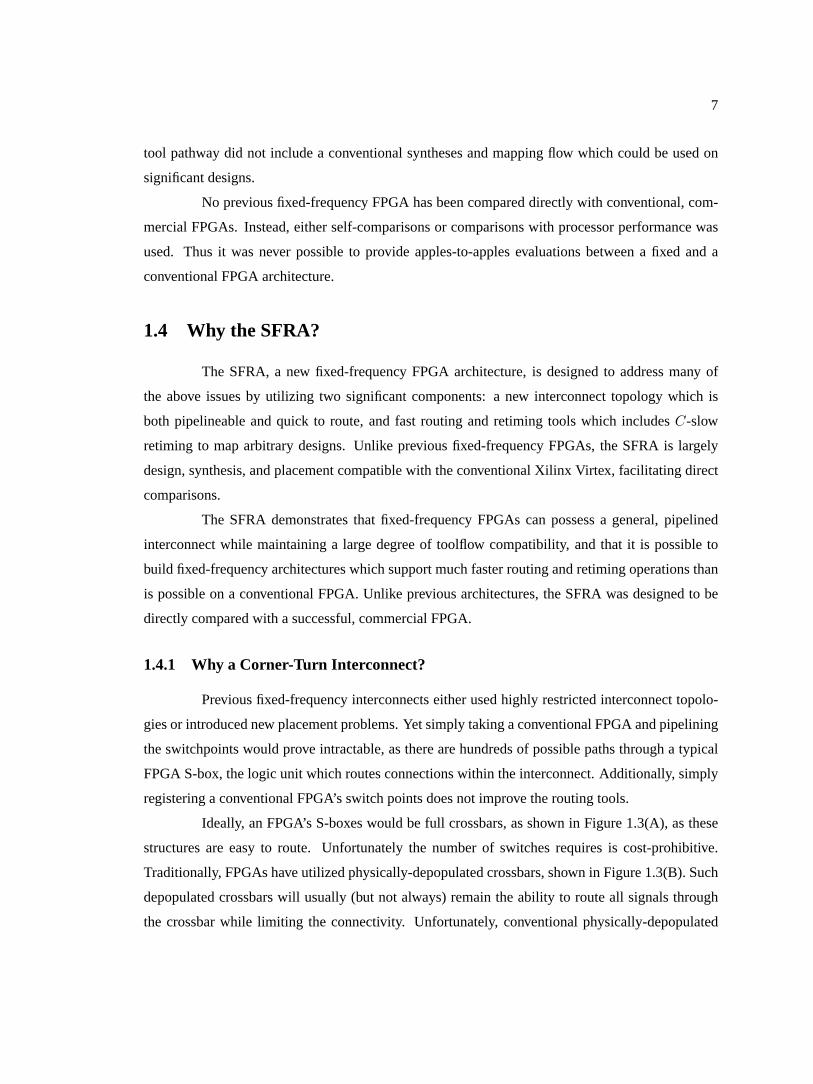
Ideally, an FPGA’s S-boxes would be full crossbars, as shown in Figure 1.3(A), as these
structures are easy to route. Unfortunately the number of switches requires is cost-prohibitive.
Traditionally, FPGAs have utilized physically-depopulated crossbars, shown in Figure 1.3(B). Such
depopulated crossbars will usually (but not always) remain the ability to route all signals through
the crossbar while limiting the connectivity. Unfortunately, conventional physically-depopulated

8
(A) (B) (C)
Figure 1.3: (A) A crossbar switch-box. (B) A physically-depopulated crossbar. (C) A capacity-depopulated crossbar.
LET
LET
LET
LET
LET
LET
LET
LET
Figure 1.4: A corner-turn FPGA interconnect. The C-boxes are implemented as full crossbars,while the S-boxes use capacity-depopulated crossbars to create corner turns, marked as T-boxes onthis illustration.
crossbars are difficult to route, while registering the switchpoints would prove excessively costly.
An alternate approach, illustrated in Figure 1.3(C), is a capacity-depopulated crossbar.
Such crossbars maintain the any-to-any connectivity of a full crossbar, but limit the number of
signals (the capacity) which can be connected.
Using capacity-depopulated crossbars, it is possible to create an alternate FPGA inter-
connect, illustrated in Figure 1.4. In a “corner-turn” network, the C-boxes remain as full cross-
bars. Additionally, all inputs and outputs to a logic element are connected to both the horizontal
and vertical channels through the C-boxes.3 Instead of using conventional S-boxes, the corner-
turn interconnect uses capacity-depopulated crossbars. The capacity-depopulated switches give the
“corner-turn” network its name, as only a limited number of signals can be routed between channels
at these switchpoints. This topology offers several advantages.
Manhattan Placement: Although the placement cost-functions should be changed, a
3Many FPGAs will connect some I/Os to only the horizontal or vertical channels.
9
corner-turn array utilizes the same placement models, tools, and techniques of a conventional FPGA.
Thus a corner-turn network, which uses a compatible logic cell, can utilize conventional FPGA
synthesis, mapping, and placement tools.
Fast Routing: Unlike a conventional FPGA interconnect, a corner-turn interconnect sup-
ports fast polynomial time routing algorithms for both global and detail routing. These algorithms
areO(n2) in the worst case, with most operations requiring onlyO(n lg n) time. Reasonably large
designs can be routed in seconds.
Pipelineable Switchpoints: Since a corner-turn network will only route a few signals
through each switchpoint, it is possible to efficiently pipeline the switchpoints with only a single
register in each direction.
Fine-grained Defect Tolerance: With some modifications of the interconnect structure,
it is possible to route around a wide variety of stuck-on and stuck-off faults in the interconnect.
Coarse-grained FPGAs: The significant area cost of a corner-turn topology, the fully
populated C-boxes, is substantially reduced for coarser-grained interconnects. Thus reconfigurable
arrays which use 8, 16, or 32 bit words can use a corner-turn network with a much lower area
penalty.
The SFRA uses this interconnect style, with regular pipelining and pipelined switches,
combined with a Xilinx Virtex derived logic element. Since the logic elements are largely compati-
ble, the Virtex synthesis, mapping, and placement tools are used to target both FPGA architectures.
Likewise, custom retiming tools created for this thesis can target both the Virtex and the SFRA.
Unlike the Virtex, the SFRA’s pipelined, fixed-frequency interconnect allows the SFRA to operate
at a much higher clock frequency, while the SFRA router is an order-of-magnitude faster than the
Virtex router.
1.4.2 WhyC-slow Retiming?
Simply adding pipelined interconnect is only half the problem, as designs must be auto-
matically modified to accommodate the additional pipeline stages. AlthoughC-slowing and retim-
ing are a well-known optimization, first proposed by Leiserson et al [41], it has not been completely
explored.
This transformation, which can be applied to arbitrary synchronous circuits, enables fine
pipelining even in the presence of feedback loops. It is based on replacing every register with a
series ofC registers and then moving the resulting registers through the design to balance delays.
10
SynplifyHDL Synthesis
Schematic
VHDL/Verilog
Xilinx VirtexTranslate & Map
ReplaceCEs
Xilinx VirtexPlacement
ResearchXilinx C-Slow
Xilinx VirtexRouting
Xilinx VirtexTiming Analysis
UnoptimizedXilinx Clock Rate
ResearchSFRA C-Slow
ResearchSFRA Router
Xilinx VirtexRouting
Xilinx VirtexTiming Analysis
OptimizedXilinx Clock Rate
ResearchSFRA C-Slow
SFRA FinalC-slow Factor
Figure 1.5: The complete toolflow created for this research. HDL designs are synthesized withSynplify, then mapped and placed using the Xilinx placement tool. At this point, one of three flowscan take place. Either the default Xilinx flow can be invoked to route and perform a timing analysis.Or the designs can be passed through the researchC-slow tool (described in Chapter 13) to improvethe Xilinx designs. The final option is toC-slow and route for the SFRA. The tools in bold werecreated for this thesis.
The resulting design now requires a factor ofC more clock cycles to complete each calculation, but
can executeC independent calculations in a parallel, round-robin fashion.
This process is generic, and can even be automatically or manually applied to such so-
phisticated structures as a microprocessor core. When applied to a processor core, a multithreaded
architecture, capable of higher throughput operation, is automatically created.
Since this process inserts pipeline stages throughout a design,C-slow retiming can meet a
fixed-frequency FPGA’s architectural constraints by determining the minimumC-factor necessary
to insure that all connections are properly pipelined.C-slowing can also be applied to designs
targeting a conventional FPGA. When applied to the benchmarks in this thesis, the automaticC-
slow tool can effectively double the throughput of Xilinx designs.
1.4.3 The Complete Research Toolflow
Figure 1.5 illustrates the complete research flow created for this project, which enables
the direct comparisons between the SFRA and the Xilinx Virtex. It is this research toolflow, with

11
components created specifically for this thesis, which enables the SFRA architecture to map designs.
Designs are first created using schematic capture or synthesis. Schematic capture was
used for the three benchmarks created specifically for this work, while synthesis was used for the
Leon SPARC benchmark. The synthesized design required a minor amount of post-synthesis editing
to accommodate minor usage restrictions needed forC-slowing.
The resulting design is first mapped, using the Xilinx mapper, and then placed on the
target FPGA. After placement, three options are possible: Unoptimized Xilinx,C-slowed Xilinx,
and the SFRA. The unoptimized Xilinx simply passes the design on to the Xilinx routing and timing
analysis tools, providing a baseline case for the Xilinx designs.
An alternate flow passes the Xilinx design through a customC-slow retiming tool, before
being passed back to the Xilinx routing and timing analysis tools. This tool, described in Chapter 13,
enables the automatic optimization of Xilinx designs throughC-slowing and retiming, and can
effectively double the throughput on the benchmarks. This flow provides an enhanced case for
Xilinx designs, allowing the effects ofC-slowing to be separated from the benefits of pipelined
interconnect.
The final toolflow accepts the Xilinx designs as input to the SFRA flow. This flow firstC-
slow retimes the design, to serve as a guide to the routing process. Then the SFRA design is routed,
before a finalC-slow retiming pass creates the final implementation. Combined with an area and
timing model, the SFRA architecture is directly comparable with both optimized and unoptimized
Xilinx toolflows. Where the SFRA tools differ from the Xilinx tools, the SFRA tools run an order
of magnitude faster than their Xilinx counterparts.
1.4.4 This Work’s Contributions
The major contributions of this work are:
• A new interconnect topology, the corner-turn interconnect, which supports much faster
routing algorithms and pipelined interconnect while maintaining syntheses and placement tool com-
patibility with previous FPGAs.
• The SFRA, a fixed-frequency FPGA architecture based on the corner-turn interconnect
topology. The SFRA is largely placement and design compatible with the commercial Xilinx Virtex
FPGA, while supporting fixed-frequency operation and substantially faster routing and retiming
tools.
• A more detailed understanding of theC-slow transformation and its general applicabil-
12
ity, including the ability toC-slow a microprocessor core to automatically produce a multithreaded
processor.
• A hand-mapped AES implementation which is one of the best cost/performance designs
available.
• An automatic tool which canC-slow designs targeting the Xilinx Virtex FPGA as well
as the SFRA. In many cases, throughput on Xilinx designs can be automatically doubled.
• A complete toolflow for the SFRA, including routing andC-slow retiming, and an
interface to the Xilinx tools for syntheses and placement. For the components where the SFRA
toolflow differs from the Xilinx toolflow, the SFRA toolflow is an order of magnitude faster.
• A direct comparison of the SFRA, a fixed-frequency architecture, with a successful
commercial FPGA, the Xilinx Virtex, using four application-based benchmarks.
1.5 Overview of Thesis
This thesis begins with a survey of previous FPGAs, both conventional and fixed-frequency,
and their strengths and weaknesses (Chapter 2). Then it provides an overview of the four application-
based benchmarks used for various experiments (Chapter 3). Three of the benchmarks were hand-
created specifically for this work, while the fourth was an acquired, synthesized design.
The first major part, Part I, details the development of the SFRA architecture and its major
motivations. This begins with an introduction to the corner-turn topology (Chapter 4). Using this
topology, the SFRA architecture is defined (Chapter 5). Then the notion of retiming registers is
introduced (Chapter 6) and the critical circuits for the interconnect are constructed (Chapter 7).
Following the architecture definition, the routing algorithms are described (Chapter 8).
These routing algorithms use heuristics which areO(n2) in the worst case, enabling routing to be
performed substantially faster when compared with a conventional FPGA. Experiments are con-
ducted with the routing tool on the four benchmarks, to determine an optimal number of turns and
other interconnect features. After routing, other implications of the corner turn topology are dis-
cussed, including defect tolerance and applicability to wider bitwidths (Chapter 9).
The thesis continues in Part II with an evaluation of retiming andC-slow retiming, which
are necessary for a fixed-frequency array to meet the target clock cycle. This part begins with a dis-
cussion ofC-slowing and retiming, first reviewing the transformation (Chapter 10), then analyzing
how it can be either automatically or manually applied to a microprocessor core to create a higher
13
performance, multithreaded architecture (Chapter 11). Given this framework, the first study evalu-
ates the effects of hand-C-slowing on the three benchmarks developed for this thesis (Chapter 12).
This study also evaluates the placement sensitivity of the Xilinx, showing how tool quality degrades
both throughput and latency.
The automatic tool toC-slow Xilinx designs is discussed and evaluated (Chapter 13).
This tool, which shares the same framework with the rest of the SFRA toolflow, can automatically
boost designs targeting the Xilinx Virtex family of FPGAs. In many cases, throughput can be
automatically doubled. This tool was evaluated on the four computational benchmarks, and the
results were also compared with the handC-slowing employed on the three hand-mapped designs.
The last part of the thesis, Part III, offers comparisons, reflections, and conclusions. Given
the SFRA architecture and a complete toolflow includingC-slow retiming and routing, the thesis di-
rectly compares the SFRA with the Xilinx Virtex (Chapter 14). The SFRA routing algorithms are an
order of magnitude faster, as are the SFRA retiming algorithms. Likewise, because of its pipelined,
fixed-frequency nature, designs would run at significantly higher throughput on the SFRA. This
thesis then concludes with an analysis of the tradeoffs between latency and throughput, and how
this is affected by FPGA architectures (Chapter 15), an examination of remaining open questions
(Chapter 16), and a final conclusions (Chapter 17).
Two appendixes appear in this thesis. The first, Appendix A provides a detailed discussion
of the AES implementation created for use as a benchmark. This design represents one of the
best cost/performance AES designs reported, and demonstrates clearly the design effort required
for high performance on current FPGAs. The second, Appendix B, surveys other multithreaded
architectures, the potential interference effects, and discusses how the architecture produced by
C-slowing relates to previous multithreaded designs.
14
Chapter 2
Related Work
2.1 FPGAs
FPGAs, Field Programmable Gate Arrays, are important computational devices. Most
FPGAs consist of a reasonably simple logic element consisting of a few lookup tables or an ALU,
with associated registers, embedded in a general purpose circuit-switched interconnect.
Since FPGAs consist of replicated computational elements, they are considerably easier
to design and fabricate when compared with other devices.1 As a result, the major commercial
FPGA vendors, Xilinx and Altera, have become process leaders [85], even when both are “fabless”
companies with no fabrication facilities of their own.
This replicated nature also leads to the impressive performance FPGAs display on a va-
riety of tasks. Each logic cell can be configured to perform a different part of the same operation
which leads to an immense amount of “spatial parallelism”, as the entire array is utilized to com-
pute a result in parallel. Additionally, since these cells include registers, the design can be pipelined,
enabling a great degree of “pipeline parallelism”.
Furthermore, since FPGAs are replicated structures, the available computation seems to
grows linearly with area. This doesn’t happen in practice, as Rent’s Rule [39] observes that larger
designs require comparatively more interconnect. Thus, more recent (and therefore larger) FPGA
families tend to utilize richer interconnect fabrics.
Yet, although silicon area is increasing, so are interconnect layers, an observation FPGA
designers have utilized. There have been proposed architectures [55] which require more metal
layers in order to scale linearly with area while matching a rents-rule growth pattern. Likewise,
1This also provides easy to test structures for process characterization.

15
F1
F2
F3
F4
G1
G2
G3
G4
Carry &Control
Carry &Control
Carry &Control
Carry &Control
LUT
CINCIN
COUT COUT
YQ
XQXQ
YQ
X
XB
YYBYB
Y
BX
BY
BX
BY
G1
G2
G3
G4
F1
F2
F3
F4
Slice 1 Slice 0
XB
X
LUTLUT
LUT D
EC
Q
RC
SP
D
EC
Q
RC
SP
D
EC
Q
RC
SP
D
EC
Q
RC
SP
BY
F5IN
SR
CLK
CE
BX
YB
Y
YQ
XB
X
XQ
G4
G3
G2
G1
F4
F3
F2
F1
CIN
0
1
1
0
F5 F5
viewslc4.eps
COUT
CY
DEC
Q
DEC
Q
F6
CK WSO
WSH
WE
A4
BY DG
BX DI
DI
O
WEI3
I2
I1
I0LUT
CY
I3
I2
I1
I0
O
DIWE
LUT
INIT
INIT
REV
REV
(A) (B)
Figure 2.1: A Virtex CLB, and the details of a single CLB-slice, from the Xilinx Datasheet [82].
commercial FPGA vendors have utilized increasing interconnect layers to meet these interconnect
requirements without substantially inflating silicon area. Thus the general observation of 1 Mλ2
per 4-LUT (with associated register and interconnect) has remained relatively consistent [22], as
the Xilinx Virtex-E series (a modern architecture with a much richer interconnect) is still only 1.25
Mλ2 per 4-LUT.2
2.1.1 Unpipelined interconnect, variable frequency
Xilinx and Altera are the primary commercial designers of FPGAs, both designing con-
ventional FPGAs without pipelined interconnect. In all these FPGAs, a design is initially mapped,
placed, and routed to the target architecture. Xilinx utilizes a Manhattan-style interconnect, while
Altera uses a cluster-based interconnect.3 Then a static timing analysis is conducted to determine
the maximum operating frequency of the resulting design.
The Xilinx Virtex series [82] is a typical example of a modern FPGA which uses a Man-
hattan style interconnect. It consists of a tiled array of logic blocks, or CLBs (Combinational Logic
Blocks). Each CLB (Figure 2.1) contains two CLB-slices, with each slice containing two 4 input
lookup tables (4-LUTs), dedicated carry logic, specialized muxes, and two registers. This structure
has been used for four FPGA families: the Virtex, the Virtex E, the Spartan II, and the Spartan IIE.
Each 4-LUT can implement an arbitrary logic function, or can act as a single port 16x1b
synchronous SRAM or a 1-16 clock, programmable delay shift-register. This shift register mode,
SRL16, is useful not only for constructing delay lines but also for specialization. Since the shift
input is separate from the address lines, a new set of LUT contents can be shifted into the LUT.
2This figure of 1.25 Mλ2 per 4-lut was calculated by directly measuring the die of a delidded Virtex-E 2000.3Although initially different, these interconnect styles are beginning to converge.

16
Additionally, the two LUTs in a slice can be combined to form a 32x1b RAM, a dual ported 16x1b
RAM, a single 5-LUT, any nine input function which can be composed with two 4-LUTs and a
mux, or two bits of an adder with the associated carry logic.
The register associated with each LUT can either be driven by the associated LUT or from
the external interconnect.4 The register has a selectable reset (either synchronous or asynchronous),
set, and clock enable, with dedicated inputs and control bits shared between the two registers in
each CLB slice.
The CLBs are embedded in a programmable interconnect fabric. Each CLB contains an
adjacent Generalized Routing Matrix (GRM) which connects the CLB to the interconnect. In both
the horizontal and vertical channels, there are 24 single-length lines which connect adjacent GRMs,
12 buffered hex lines in each direction which are connected to the GRMs 6 CLBs away in each of
the 4 directions, and 12 buffered longlines for high fanout, long distance signals. Thus the Virtex’s
routing channel can contain up to 108 signals in addition to dedicated connections between CLBs.
Although there are considerable amount of wires per logic element, this number is fairly
typical. As FPGAs have grown larger, the relative amount of interconnect has also increased. This
is largely due to larger designs following Rent’s Rule [39], and therefore require more interconnect
to successfully map larger designs.
Also included in the fabric are columns of BlockRAMs, dual ported 4 Kb SRAMs. Each
of the ports can be independently configured to be 1, 2, 4, 8, or 16 bit wide. They are arranged
in vertical columns, with a pitch of 1 BlockRAM per 4 CLBs. The Virtex E and EM series parts
contain multiple BlockRAM columns spaced throughout the chip, while the other members only
contain 2 columns, one on each side of the chip.
The Virtex 2 [83], a successor to the Virtex family, uses a larger CLB containing eight
4-LUTs and flip-flops, an even richer interconnect, and larger BlockRAMs. The basic intercon-
nect structures are similar, but there are considerably more wires in the channels. The Virtex 2
BlockRAMs also contain associated 18x18→36 bit pipelined multipliers which share I/O and rout-
ing resources, in order to provide embedded pipelined multipliers without adding to interconnect
requirements.
A previous limitation of the Virtex’s Manhattan structure was a limited ability to integrate
larger fixed blocks. With the Virtex, the only integrated blocks were the BlockRAMs in regular
vertical stripes. The Virtex II, by using more layers of interconnect and reserving the upper inter-
4The only exception is that the register can not be used independently of the LUT at the lowest bit of the carry chainor when the F5 or F6 muxes are utilized.
17
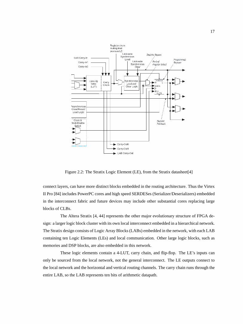
Figure 2.2: The Stratix Logic Element (LE), from the Stratix datasheet[4]
connect layers, can have more distinct blocks embedded in the routing architecture. Thus the Virtex
II Pro [84] includes PowerPC cores and high speed SERDESes (Serializer/Deserializers) embedded
in the interconnect fabric and future devices may include other substantial cores replacing large
blocks of CLBs.
The Altera Stratix [4, 44] represents the other major evolutionary structure of FPGA de-
sign: a larger logic block cluster with its own local interconnect embedded in a hierarchical network.
The Stratix design consists of Logic Array Blocks (LABs) embedded in the network, with each LAB
containing ten Logic Elements (LEs) and local communication. Other large logic blocks, such as
memories and DSP blocks, are also embedded in this network.
These logic elements contain a 4-LUT, carry chain, and flip-flop. The LE’s inputs can
only be sourced from the local network, not the general interconnect. The LE outputs connect to
the local network and the horizontal and vertical routing channels. The carry chain runs through the
entire LAB, so the LAB represents ten bits of arithmetic datapath.

18
Unlike the Xilinx CLB, there are more restrictions involving packing flip-flops with un-
related logic as seen in Figure 2.2. Each LE has three outputs: local (for within LAB routing),
horizontal, and vertical routing. These outputs can either be driven by the Flip-Flop or LUT, but not
both. Similarly, the Flip-Flop’s independent input is shared with one LUT input, further restrict-
ing the cases where the Flip-Flop can be used independently. This would restrict the retiming tool
described in Chapter 13.
The interconnect in the Stratix is based on horizontal and vertical channels, with various
segment lengths within each channel. These wires can be driven by the LE outputs as well as
sourced from the other channel to enable routing. LE inputs are only drivable from the LAB local
routing, requiring that all signals in the main routing channels be routed onto the local connections
before driving the LEs. In previous Altera parts [2], this local interconnect was a full crossbar, but
the Stratix depopulates the input crossbars.
This routing structure is well suited for less structured designs, but poses some prob-
lems for high performance signal processing and similar arithmetic-heavy tasks. In most FPGAs,
dataflow is arranged with the data moving horizontally, perpendicular to vertical carry-chains. Yet
in the Stratix and similar cluster-based architectures, the bits need to be routed onto the horizontal
channel and then onto the local interconnect before they can be used in the next stage of compu-
tation. Since datapaths are often bit-aligned when either hand or automatically constructed, this
can add significant routing delays. This problem is reduced, but not eliminated, through the use of
additional direct LAB to LAB paths.
The Stratix architecture embeds significantly larger memory blocks in the design as well.
Only some of the interconnect wires (the longer horizontal and vertical connections) are routed over
the largest of the blocks. The Stratix GX [5] also embeds high speed SERDESes similar to those in
the Virtex 2 Pro.
2.1.2 Unpipelined Interconnect Studies
There have been numerous published studies of various interconnect topologies for use
within conventional FPGAs. One such study, by Xilinx [52], developed the concept of “Octlines”,
length 8 interconnect segments with restricted outputs, designed to provide a reasonably fast-path
for signals which travel a moderate distance. This structure evolved into the Hexlines used in the
Virtex and Virtex II FPGAs.
Likewise, Altera has published several studies, including enhancements used to create the

19
Mercury architecture [34] and the Stratix architecture [44]. For the Mercury architecture, most of the
improvements were achieved by providing different wire types which, with the same connectivity,
offered faster performance. Thus the router could prioritize critial paths, routing them onto faster
nets. This allowed for substantial reductions in the critical path.
The Stratix architecture used a comprehensive approach to define the interconnect, by first
developing a model of the various resources and then evaluating for an optimal position on various
benchmarks. One major contribution was depopulating the LAB (Local Area Block) connections
from full crossbars to partial crossbars, a technique first described in Lemieux and Lewis [43] as an
extention to the related work [42] on depopulating switchpoints.
Schmidt and Chandra [58] attempted to analyze the benefits of different switchbox strate-
gies and their resulting impact on area, while Lemieux et al [43] was concerned with depopulating
switchboxes while maintaining routability.
2.1.3 Pipelined Interconnect, Variable Frequency
There have been two proposed architectures which contain pipeline interconnect without
maintaining a fixed-frequency property. In both cases, tools must utilize the interconnect pipelining
to improve performance.
The first, by Singh and Brown[62], has interconnect switches which include optional
registers to pipeline longer connections. Their design began with a simplified FPGA consisting of 4-
LUTs and associated flip-flops, and then performs retiming during the routing process to determine
whether to use a registered switch.
The significant contributions involve the architecturally constrained retiming and retim-
ing aware routing in order to utilize the new registered interconnect pieces. Unfortunately, their
basic logic cell does not have an independently-utilizable flip-flop, which limits the quality of their
baseline retiming which was used in the comparisons. This work also did not includeC-slowing or
repipelining in order to exploit the greater degree of potential pipelining, but such a transformation
could be easily added to their toolflow.
Singh et al’s wave-pipelined FPGA [61] is a high-frequency FPGA using pipelined inter-
connect. This architecture utilizes a pipelined LUT as well as interconnect, targeting high frequency
operations. This array uses registered switchpoints, with each interconnect segment only able to
traverse 4 LUTs before being registered. This array lacks retiming facilities, as well as tools to
automatically repipeline the design.

20
2.1.4 Pipelined, fixed frequency
There have been numerous fixed-frequency architectures, however they have all suffered
from various limitations.
The Garp [30, 31] was a design for a reconfigurable co-processor meshed with a micropro-
cessor. In order to allow integration, it was designed to always operate at the same clock frequency
as the processor. In order to support fixed-frequency operation, all LUT outputs were registered and
there was no routing resources on the interconnect.
Garp’s interconnect consisted of dedicated horizontal and vertical connections, with the
data flowing vertically. The horizontal lines were single-driver, multiple sink, and used to institute
fixed and variable shifts. The vertical lines were broken at regular intervals to facilitate routing.
Any routing between horizontal and vertical interconnect occurred through a logic cell. This lack
of switching enabled Garp to operate at a defined frequency, as no signal could ever traverse more
interconnect than the allotted cycle. Garp’s tool flow did not support automatic repipelining, but
as it was intended primarily for datapaths, the retiming problem was fairly simple and left to either
human designers or upstream tools such as Gama [15].
A logical successor to Garp’s array is the PiCoGa [46], a fixed-frequency architecture
designed to be more tightly coupled in a microprocessor pipeline. This system utilizes a VLIW
processor with a reconfigurable coprocessor. A novel feature of the reconfigurable array is that
every row’s registers are only active when the row is being used for a computation as a power-
saving mechanism. The interconnect is switched but not pipelined, and there are undoubtedly limits
on how far signals can travel within a clock cycle, but these aren’t stated in the current publications.
RaPiD [24] also used a fixed-frequency design. RaPiD consisted of heterogeneous logic
units connected by a 1-D interconnect channel. Any connection which would have exceeded the
architecture’s delay was routed to a register and then back onto the interconnect, through special
register units. Although RaPiD is fixed-frequency, the fixed-frequency property is enforced by the
tools [60], not the interconnect architecture. Long delays must pass through dedicated register-block
resources to match the timing constraints.
PipeRench [57] is another fixed-frequency array designed for computational use. In order
to operate at a fixed frequency and to enable virtualization, only feed forward designs can be mapped
to this interconnect. At each stripe, all data is registered, with some being computed on and others
simply being forwarded to the next stripe. Since the array is designed to map only feed-forward
designs, the interconnect flexibility is deliberately limited.
21
HSRA [74] was the first attempt to produce a general purpose fixed-frequency FPGA
designed to map all designs where pipeline or task level parallelism is available. HSRA used a
conventional 5-LUT embedded in an H-tree with shortcuts. At the branches of the H-tree, the
switches were diagonally populated. Some levels used pipeline registers, to ensure that every path
was properly registered.
In order to balance these delays, post-placementC-slow retiming was employed by call-
ing out tosis [23] and retiming the resulting design. Since the H-tree design produces determin-
istic routing delays, only a singleC-slowing pass is required. All LUT inputs contain retiming
registers to balance out the delays.
The greatest limitations of the HSRA arise from the toolflow requirements. The H-tree
interconnect introduced a new placement problem, and it is especially unclear how to place datap-
aths onto this structure. Additionally, the HSRA presented a new and challenging routing problem,
which appears to be of comparable difficulty when compared with a conventional FPGA.5 This
array also did not have support for a synthesis pathway or an optimized retiming tool.
2.2 FPGA Tools
Quality FPGAs do not simply require good architectures, but also require high quality
tools for placement, routing and possibly retiming. Without tools, an FPGA architecture cannot
be effectively utilized. In general, tools first map the design to the target’s components, place the
mapped design on the array, and then route the connections. Following the complete placement and
routing process, a conventional FPGA toolflow performs a static timing analysis to determine the
design’s maximum clock frequency.
2.2.1 General Placement
Conventional placement has often relied on simulated annealing or other heuristics. A
good example is the VPR [11] academic placement and routing tool. VPR uses simulated anneal-
ing placement, a probabilistic approximation to pack related logic units close together. Simulated
annealing is generally highly effective for placing theses sorts of designs.
These heuristics are commonly deployed in commercial placement tools by Xilinx and
Altera, as they work reasonably well on most designs. The general limitation, as discussed in
5In practice, the best HSRA routing results use the Pathfinder [47] FPGA routing algorithm.

22
Chapter 3, arises when high performance datapaths are desired.
Simulated annealing operates by assigning a cost function for each connection, usually
as a function of distance with priority given for critical links. During each iteration, many moves
are contemplated. If the move will result in a cost reduction, it is taken. If the move would result
in an increase in cost, a probabilistic decision is conducted based on the cost of the move and the
temperature, a measure of how likely unfavorable moves will be taken. The temperature begins at a
high level, enabling most bad moves to be accepted, before it is slowly lowered to zero.
2.2.2 Datapath Placement
Datapaths benefit substantially from datapath oriented placement. Koch’s system [38]
composed a datapath by placing bit-slices in order, then tiling the slices to create the full datapath
width. Heuristics were used for the one dimensional placement of the elements in the datapath, in
an attempt to maintain a mostly feed-forward dataflow.
Similarly, Gama [15], the mapping portion of the Garp/CC C compiler targeting the
GARP reconfigurable processor, used bottom-up rewrite grammars [27] to map and place designs
into an aligned datapath. This process selects the proper operators (including combining associ-
ated objects) and places them in an aligned datapath, attempting to minimize both the number of
operators and minimizing the distance between operators.
Finally, there have been many generator systems [79, 19, 48, 80, 9, 64] which have in-
cluded placement ability. These systems are used by programmers to create procedures to construct
design instances. As a result, most systems encourage bottom-up construction techniques where
adjacent operators are aligned and placed next to each other. When generators include the ability to
specify placement directives, clean datapath layouts tend to be produced as programmers logically
construct a hierarchical structure.
Datapath placement is generally effective because the problem is considerably simpler.
For a datapath, a one-dimensional placement is usually very effective, as there is a natural vertical
alignment for all components. This is specifically observed in Chapter 12, where the synthetic dat-
apath (consisting of discrete but pre-placed elements) can be successfully laid out by the automatic
tools as it is a one-dimensional, not a two-dimensional placement problem.
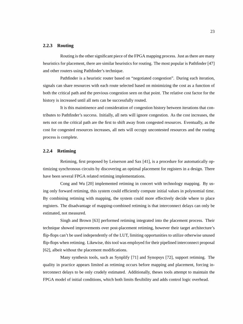
23
2.2.3 Routing
Routing is the other significant piece of the FPGA mapping process. Just as there are many
heuristics for placement, there are similar heuristics for routing. The most popular is Pathfinder [47]
and other routers using Pathfinder’s technique.
Pathfinder is a heuristic router based on “negotiated congestion”. During each iteration,
signals can share resources with each route selected based on minimizing the cost as a function of
both the critical path and the previous congestion seen on that point. The relative cost factor for the
history is increased until all nets can be successfully routed.
It is this maintinence and consideration of congestion history between iterations that con-
tributes to Pathfinder’s success. Initially, all nets will ignore congestion. As the cost increases, the
nets not on the critical path are the first to shift away from congested resources. Eventually, as the
cost for congested resources increases, all nets will occupy uncontested resources and the routing
process is complete.
2.2.4 Retiming
Retiming, first proposed by Leiserson and Sax [41], is a procedure for automatically op-
timizing synchronous circuits by discovering an optimal placement for registers in a design. There
have been several FPGA related retiming implementations.
Cong and Wu [20] implemented retiming in concert with technology mapping. By us-
ing only forward retiming, this system could efficiently compute initial values in polynomial time.
By combining retiming with mapping, the system could more effectively decide where to place
registers. The disadvantage of mapping-combined retiming is that interconnect delays can only be
estimated, not measured.
Singh and Brown [63] performed retiming integrated into the placement process. Their
technique showed improvements over post-placement retiming, however their target architecture’s
flip-flops can’t be used independently of the LUT, limiting opportunities to utilize otherwise unused
flip-flops when retiming. Likewise, this tool was employed for their pipelined interconnect proposal
[62], albeit without the placement modifications.
Many synthesis tools, such as Synplify [71] and Synopsys [72], support retiming. The
quality in practice appears limited as retiming occurs before mapping and placement, forcing in-
terconnect delays to be only crudely estimated. Additionally, theses tools attempt to maintain the
FPGA model of initial conditions, which both limits flexibility and adds control logic overhead.

24
The initial condition problem for FPGA retiming is more complex than that solved by
Cong and Wu, as FPGAs generally posess a global set-reset functionality with dedicated intercon-
nect. Thus conventional retiming tools need to include additional logic in the datapath to handle
startup, as some registers can’t be allowed to transition for several cycles after the reset to ensure
proper order. These control structures often add delay onto the critical path, and require more FPGA
resources, generally ofsetting many of the benefits of retiming.
25
Chapter 3
Benchmarks
For evaluating the SFRA architecture, high performance tools, and the effects of datapath
placement, four benchmark designs were utilized: AES Encryption [50], Smith/Waterman [67]
sequence matching, a synthetic microprocessor datapath, and the LEON I synthesized SPARC core
[54].
The first three designs, created as part of this thesis, were all hand-mapped to the Virtex
family of FPGAs and implemented using schematic capture, with both hand placement and au-
tomatic placement, as well as handC-slowed implementations. Thus, these applications can be
directly used to evaluate the quality of placement and retiming tools. The final benchmark, Leon,
was a synthesized, publically available design1 acquired from the Internet site of Gassier Research.
Schematic capture was used on the hand-mapped benchmarks for two reasons: familiarity
and precision. Natural familiarity makes high-performance designs easier as there is less time spent
manipulating tools. More importantly, high performance FPGA designs tend to be directly mapping
to the target architecture, specifying the LUT logic and placement for all of the datapath and even
some of the control logic. Thus, many of the higher level transformations of a synthesis tool are
unnecessary.
3.1 AES Encryption
The recently adopted AES (Advanced Encryption Standard) block cipher [50], based on
the Rijndael encryption algorithm, offers solid performance in both software and hardware, with
hand-coded assembly implementations able to encrypt at over 1 Gbps on a 3 GHz Pentium 4 [45] and
1The Leon core is released under the LGPL liscence which allows free derivitive works
26
published FPGA implementations which, with suitable area, achieve multigigabit encryption rates.2
Because of the expected widespread adoption, both within the federal government and private sector,
AES is expected to be the most commonly implemented block cipher over the next twenty years.3
Because of its growing ubiquity and versatility as a block cipher, it is an excellent candidate for
implementations in hardware.
For benchmarking, an aggressive AES core was implemented. This core is a single en-
cryption round, with 5 stages of pipelining to create aC-slowed design. This design is “key-agile”,
as it accepts both a 128 bits of key and 128 bits of data simultaneously. The 5-slow version can be
encrypting 5 data blocks simultaneously, with each block able to use a different key. The design
was also hand-placed, with almost every element specified to match the general dataflow.
AES was selected as a benchmark for several reasons: it consists of mostly bit and word
oriented operations, the interconnect requirements are fairly complex, and AES is at the core of most
security applications. The bit and word mixing doesn’t exercise arithmetic operations, but they do
exercise most other FPGA features including pipelining, LUTs, small delay-chains, and larger em-
bedded memories. Although there is a large degree of high-level structure, this structure generally
dissapears when the application is viewed at the bit-level, due to the various permutations required.
This lack of structure on the micro-level makes AES more difficult to route when compared with
other datapaths.
Performance for the throughput optimized version with a 128 bit key ranges from a 115
MHz clock rate with 1.3 Gbps throughput4 for non-feedback modes on a Spartan 2 100-5 (a∼$10
part in large quantities5) to 155 MHz clock with 1.75 Gbps throughput for a Virtex E-600-8. This
design requires 10 BlockRAMs and 800 CLB slices for a fully key-agile encryption core, which
is less than 1/2 the area of a comparable HDL synthesis implementation.6 This design also offers
superior performance when compared with published commercial implementations.
The latency optimized version (withC-slowing removed) with a 128 bit key runs at 45
MHz in the same Spartan 2 100-5, giving a throughput of 520 Mbps regardless of the feedback
mode, using 10 BlockRAMs and 460 CLB slices. More details on this design, including compar-
isons with other commercial and academic implementations, are available in Appendix A.
2This contrasts sharply with DES who’s bit-oriented, permutation based design is significantly faster in hardwarewhen compared with software.
3Although 3DES [76] may remain in use for a considerable period of time, most new implementations are expectedto select AES.
4It requires a 3 GHz Pentium 4, with hand-coded assembly, to match this performance in software [45]5The even faster Spartan 2E of the same size is available for $25 in single unit quantities from Digikey.6This core is freely available at http://www.cs.berkeley.edu/∼nweaver/rijndael
27
Figure 3.1: Layout of an individual systolic cell for the Smith/Waterman sequence matchingcomputation
3.2 Smith Waterman
The Smith/Waterman edit distance calculation as used for biological sequence matching
[67] is a well-known application for reconfigurable computing [14]. It is a systolic computation
which compares a source string with destination strings in a database and computes an edit distance
needed to convert the source string to the destination string. It is a staple algorithm in bioinformatics,
where one wishes to search for similar DNA sequences or proteins in a large database. Several
custom machines have been built for the purpose of accelerating this and similar algorithms [14, 73,
53]. Since the general usage requires comparing a single entry against a large database, this matches
well with C-slowed semantics discussed in detail later in this thesis.
Smith/Waterman, when implemented in FPGA logic, consists of table lookups, arithmetic
comparisons, multiplexing, and additions in a systolic cell, to calculate two values,Ii,j andMi,j
for two strings, and to determine the maximum value ofM . The parametersi,j is based on the
related nature of the corresponding characters7 in the string whiled ande are the cost of creating or
extending a gap between the two strings. The result calculates a highly accurate approximation of
the similarity of two sequences.
7This reflects that some protein substitutions will result in very minor deformations (costs), while other changes willsignificantly deform the resulting structure.
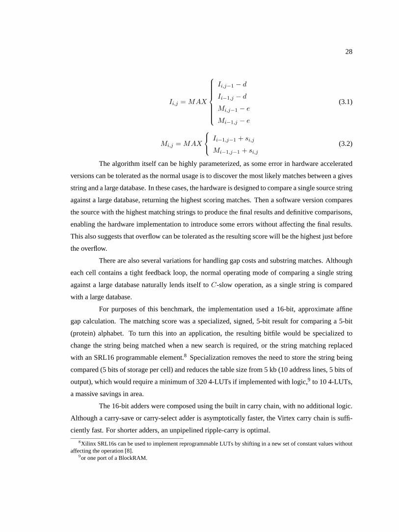
28
Ii,j = MAX
Ii,j−1 − d
Ii−1,j − d
Mi,j−1 − e
Mi−1,j − e
(3.1)
Mi,j = MAX
Ii−1,j−1 + si,j
Mi−1,j−1 + si,j
(3.2)
The algorithm itself can be highly parameterized, as some error in hardware accelerated
versions can be tolerated as the normal usage is to discover the most likely matches between a gives
string and a large database. In these cases, the hardware is designed to compare a single source string
against a large database, returning the highest scoring matches. Then a software version compares
the source with the highest matching strings to produce the final results and definitive comparisons,
enabling the hardware implementation to introduce some errors without affecting the final results.
This also suggests that overflow can be tolerated as the resulting score will be the highest just before
the overflow.
There are also several variations for handling gap costs and substring matches. Although
each cell contains a tight feedback loop, the normal operating mode of comparing a single string
against a large database naturally lends itself toC-slow operation, as a single string is compared
with a large database.
For purposes of this benchmark, the implementation used a 16-bit, approximate affine
gap calculation. The matching score was a specialized, signed, 5-bit result for comparing a 5-bit
(protein) alphabet. To turn this into an application, the resulting bitfile would be specialized to
change the string being matched when a new search is required, or the string matching replaced
with an SRL16 programmable element.8 Specialization removes the need to store the string being
compared (5 bits of storage per cell) and reduces the table size from 5 kb (10 address lines, 5 bits of
output), which would require a minimum of 320 4-LUTs if implemented with logic,9 to 10 4-LUTs,
a massive savings in area.
The 16-bit adders were composed using the built in carry chain, with no additional logic.
Although a carry-save or carry-select adder is asymptotically faster, the Virtex carry chain is suffi-
ciently fast. For shorter adders, an unpipelined ripple-carry is optimal.
8Xilinx SRL16s can be used to implement reprogrammable LUTs by shifting in a new set of constant values withoutaffecting the operation [8].
9or one port of a BlockRAM.
29
Each systolic cell matches a single character to the database, and is connected only to its
nearest neighbors in a 1-D arrangement. The layout of the cell itself is straightforward, with a simple
left-to-right dataflow within the cell and all operations aligned. The value forsi,j is generated below
the cell. The cells are then arranged in a serpentine pattern to fill up the chip, while minimizing the
communication distance between cells.
The C-slowed version used 4 stages per cell, representing a 4-slow design. This was
determined by experimentation. A 3-slowed version did not have quite the performance desired,
while adding a 5th stage could not reduce the critical path.
3.3 Synthetic microprocessor datapath
Although with the advent of commercial microprocessor/FPGA hybrids [1, 84], as well
as highly specialized commercial FPGA soft cores [86, 3], there is less call to implement a micro-
processor using FPGA logic, portions of microprocessors are an excellent test of an FPGA’s ability
to perform arithmetic, multiplexing, memory, and control logic.
The datapath portion of a microprocessor is highly regular, requiring fast arithmetic op-
erations, fast multiplexing operations, and considerable pipeline registers. The register file needs
small, very fast memories, while the instruction and data caches need larger memories. The datapath
is laid out in a regular fashion, matching the classic viewpoint.
For the purposes of this benchmark, the datapath targeted a conventional 5-stage pipeline
for a 32-bit simplified MIPS like instruction set with a 2-KB data cache. Arithmetic operations
(addition, subtraction, and bitwise operations) are single cycle latency, with shifts taking 2 cycles
and memory reads requiring 3 cycles of latency. The manditory input register on the BlockRAMs
result in the additional latency for memory operations. Similarly, the latency for the shift operations
is due to the heavy interconnect cost and several levels of logic needed to implement a bidirectional
shifter.
Since this datapath operates on 32-bit quantities, the adder/subtracter uses a 16-bit carry-
select construction. Carry-select was chosen, because it matches well with the target architecture,
allowing the 16 bit subadders to use the carry chain. More importantly, a carry-select adder can be
more easily pipelined when compared to a ripple-carry structure in the Xilinx architecture.
As seen in Chapter 11, aC-slowed microprocessor produces an interleaved-multithreaded
architecture. TheC-slowed version uses 3 streams of execution, or aC-slow factor of 3, as this
matched well with the already finely pipelined microprocessor datapath.
30
Due to the size of the BlockRAMs for the register file when compared with the logical
size of the register file, the memories were not increased in size, as this wasn’t necessary to complete
the transformation. Since this benchmark is designed to evaluate the datapath portion, it does not
include the control logic needed to complete a processor.
3.4 LEON Synthesized SPARC core
Many FPGA designs use HDL synthesis. Such designs rely on automatic translation from
a high level description, usually VHDL or Verilog. These designs also rely on automatic placement
and routing. Traditionally, there is a substantial performance penalty for designs which rely heavily
on synthesis.10
The Leon I [54] microprocessor core is used as a synthesized benchmark for evaluating
theC-slowing tool and SFRA architecture. This design is a fully synthesized SPARC compatible
integer processor requiring roughly 6000 LUTs. In order to create a design suitable for benchmark-
ing, the caching and external interfaces were removed and replaced with dummy connections to
external I/Os. These connections keep the rest of the design from being optimized away.
To enable automaticC-slowing and SFRA mapping, the register file (a synthesized struc-
ture) was replaced with an instanced BlockRAM-based register file. Since the Leon core assumes
that the register file’s memory is asynchronous, the BlockRAM uses a negative-edge clock. This
preserves the register file semantics, although it may have a performance impact, if the BlockRAM
access is not in the middle of the processor cycle.
The design was synthesized with clock-enables suppressed, and the EDIF netlist was
manually edited to convert register resets to explicit logic. This editing simply replaced the primitive
EDIF components with a LUT and register combination before letting the back-end tools map the
design. Both of theses changes are needed to allow automaticC-slowing without modifying the
placement when targeting both the Virtex and the SFRA, as all these features need to be expressed
as LUT logic rather than as register-specific features.
10Although many high performance designs may use VHDL or Verilog, most of these designs use the HDL as a textualrepresentation of FPGA features creating designs which are very similar to those produced by schematic capture.
31
3.5 Summary
Four benchmarks are used throughout this thesis. The first three, AES Encryption, Smith/
0Waterman sequence matching, and the synthetic datapath, were all implemented with hand place-
ment and handC-slowing in order to gauge the sensitivity and quality of both placement and retim-
ing tools. The last benchmark, the Leon processor core, represents a typical design utilizing HDL
synthesis.

32
Part I
The SFRA Architecture

33
This section of the thesis is focused on the development of the SFRA architecture. This
begins with an introduction to the corner-turn topology in Chapter 4. Unlike conventional FPGA
topologies, this topology can be efficiently pipelined and supports fast routing algorithms.
Using this topology, the SFRA architecture is defined in Chapter 5. Although a new FPGA
architecture, the SFRA is largely placement and design compatible with the Xilinx Virtex, which
facilitates later comparisons.
Then the notion of retiming registers is introduced in Chapter 6. This chapter introduces
a new option, “mixed-retiming”, and compares it with the previously evaluated input and output
retiming. Although the SFRA uses input retiming, it was only after evaluating mixed-retiming that
the decision was finalized.
The critical circuits for the SFRA interconnect are constructed in Chapter 7. Although
only the interconnect is constructed, this defines both the critical path and critical area for the SFRA.
A 300 MHz clock cycle appears easily achievable in a .18µm process.
Following the architecture definition, the routing algorithms are described in Chapter 8.
These routing algorithms use heuristics which areO(n2) in the worst case, enabling routing to be
performed substantially faster when compared with a conventional FPGA. Experiments are con-
ducted with the routing tool on the four benchmarks, to determine an optimal number of turns and
other interconnect features.
After routing, other implications of the corner turn topology are discussed, including de-
fect tolerance and applicability to wider bitwidth in Chapter 9. Although the SFRA doesn’t utilize
these additional benefits, other corner-turning FPGAs might utilize these additional corner-turn re-
lated features.

34
Chapter 4
The Corner-Turn FPGA Topology
4.1 The Corner-Turn Interconnect
Manhattan-structured FPGAs, as commonly visualized in Figure 4.1, consist of 3 main
pieces: logic elements (LEs) that perform the actual computation, connection boxes (C-boxes) that
connect the logic elements to the general interconnect, and switch boxes (S-boxes) used to route
signal in the general interconnect. Parameters include the number of signals in each channel (the
channel capacity), and the number of bits in each signal (the bitwidth or granularity).
If routability were the only criterion, the C-boxes and S-boxes would both be full cross-
bars, as in Figure 4.2(A), enabling the C-boxes to use any wire as an input or output and the S-boxes
to connect any input to output. Unfortunately, crossbars, especially for the S-boxes, are usually too
expensive, as they requireO(N2) switches to implement a channel capacity ofN bits.
LEC-Box
C-B
oxS-Box
LEC-Box
C-B
oxS-Box
LEC-Box
C-B
oxS-Box
LEC-Box
C-B
oxS-Box
LEC-Box
C-B
oxS-Box
LEC-Box
C-B
oxS-Box
LEC-Box
C-B
oxS-Box
LEC-Box
C-B
oxS-Box
Figure 4.1: The classical components of a Manhattan FPGA: the LE (logic element) performs thecomputation, the C-box (connection box) connects the LE to the interconnect, and the S-box (switchbox) provides for connections within the interconnect.
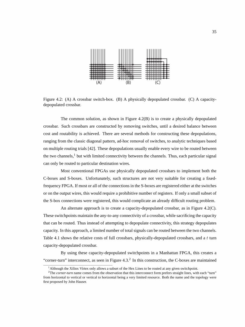
35
(A) (B) (C)
Figure 4.2: (A) A crossbar switch-box. (B) A physically depopulated crossbar. (C) A capacity-depopulated crossbar.
The common solution, as shown in Figure 4.2(B) is to create a physically depopulated
crossbar. Such crossbars are constructed by removing switches, until a desired balance between
cost and routability is achieved. There are several methods for constructing these depopulations,
ranging from the classic diagonal pattern, ad-hoc removal of switches, to analytic techniques based
on multiple routing trials [42]. These depopulations usually enable every wire to be routed between
the two channels,1 but with limited connectivity between the channels. Thus, each particular signal
can only be routed to particular destination wires.
Most conventional FPGAs use physically depopulated crossbars to implement both the
C-boxes and S-boxes. Unfortunately, such structures are not very suitable for creating a fixed-
frequency FPGA. If most or all of the connections in the S-boxes are registered either at the switches
or on the output wires, this would require a prohibitive number of registers. If only a small subset of
the S-box connections were registered, this would complicate an already difficult routing problem.
An alternate approach is to create a capacity-depopulated crossbar, as in Figure 4.2(C).
These switchpoints maintain the any-to-any connectivity of a crossbar, while sacrificing the capacity
that can be routed. Thus instead of attempting to depopulate connectivity, this strategy depopulates
capacity. In this approach, a limited number of total signals can be routed between the two channels.
Table 4.1 shows the relative costs of full crossbars, physically-depopulated crossbars, and at turn
capacity-depopulated crossbar.
By using these capacity-depopulated switchpoints in a Manhattan FPGA, this creates a
“corner-turn” interconnect, as seen in Figure 4.3.2 In this construction, the C-boxes are maintained
1Although the Xilinx Virtex only allows a subset of the Hex Lines to be routed at any given switchpoint.2Thecorner-turnname comes from the observation that this interconnect form prefers straight lines, with each “turn”
from horizontal to vertical or vertical to horizontal being a very limited resource. Both the name and the topology werefirst proposed by John Hauser.

36
Parameter Crossbar, Crossbar, k depopulated k depopulated t turnregistered registered Crossbar, Crossbar, switchswitches outputs registered registered
switches outputsEncoded ConfigurationBits 2n2 (n + 2)n 2kn (k + 2)n 4t lg n
Registers n2 2n kn 2n 2t
Parasitic CapacitanceOn A Wire n n k k 2t
Parasitic CapacitanceOn A Connection 2n 2n 2k 2k 2n
Table 4.1: Comparing the costs of a full crossbar,k physically-depopulated crossbar, and at turncapacity-depopulated crossbar for ann by n channel intersection.
LET
LET
LET
LET
LET
LET
LET
LET
Figure 4.3: A corner-turn FPGA interconnect. The C-boxes are implemented as full crossbars,while the S-boxes use capacity-depopulated crossbars to create corner turns, marked as T-boxes onthis illustration.
as full crossbars, with each input and output connected to both the associated horizontal and vertical
channels. The S-boxes are replaced with T-boxes, capacity-depopulated crossbars with the capacity
described as the number of turns supported. Each turn is able to route a signal from the horizontal
to the vertical channel direction and a separate signal from the vertical to the horizontal channel.
For simplicity, it is assumed that the C-boxes are full crossbars. This assumption makes
it easy to perform fast detailed routing and guaranteed detail-routing overhead at the cost of some
efficiency. (As discussed later, it may be possible to depopulate the C-boxes without sacrificing fast
detailed routing, but this issue has been deferred for later research.)
Unlike conventional switchpoints, there are several advantages to a corner-turn topology
that result from the use of reduced-capacity S-boxes instead of physically depopulated S-boxes and
full-crossbar C-boxes:
37
Fast Routing: As detailed in Chapter 8, both global and detailed routing use fast, poly-
nomial time heuristics. Detailed routing uses known techniques, while global routing uses new
algorithms. No step is worse thanO(n2) in the worst case, while most steps areO(n lg n) or better.
Fixed Routing Overhead: Given a global channel congestion and a wire break schedule,
there is a maximum overhead which detailed routing may impose. In practice, the overhead is
substantially lower.
Pipelined Switchpoints: If a conventional crossbar or depopulated crossbar were to use
pipelined switchpoints, it would require numerous pipeline registers. A corner-turn switchpoint,
however, requires only two registers for each turn, a substantial savings. This savings is particularly
useful, given the goal to implement a fixed-frequency FPGA.
Potential Defect Tolerance: Any resource that can be exchanged for another offers the
potential for defect tolerance. It is obvious that, with an additional turn and spare wires, breaks in
the T-boxes and routing channels can be overcome by simply remapping the wires in question from
a defective connection to a working connection.
If the interconnect uses a classical braiding pattern, many faults in the C-boxes cannot
be avoided. However, if all wires in a channel have breaks, rebuffering, or registers at the same
places, then a large number of stuck-on and stuck-off faults in the C-boxes can be routed around by
transposing connections.
Asymmetric Routing Channels: In Hallschmid [29] and elsewhere, it has been argued
that asymmetric routing channels, where the horizontal and vertical capacities are significantly dif-
ferent, may have significant advantages.3 The corner-turn structure is highly amenable to asymmet-
ric channel without changing the routing problem. As a related observation, if a design following
Rent’s Rule is mapped to a Manhattan FPGA using common placement techniques, more intercon-
nect will be required near the center of the FPGA.
Because the corner-turn switches maintain any-to-any connectivity, it is easy to construct
and route arrays where the routing channels closer to the periphery utilize fewer wires. Such arrays
do not affect the routability beyond the capacity limits, as each channel is detail-routed indepen-
dently. As the bulk of any FPGA lies in the wiring and switching, this strategy offers potentially
large area savings.
Finally, as seen in Chapter 5, the bit-oriented SFRA based on the corner turn topology
is substantially larger than commercial FPGAs although competitive with previous fixed-frequency
3Although Betz and Rose [10] that asymmetric routing channels are not that effective.
38
FPGAs. This disadvantage disappears when the array’s basic operations occur on larger quantities.
Thus for arrays that operate on 8-bit or 16-bit bit quantities such as those used by Chameleon
[16], Matrix [49] and others, a corner-turn interconnect may be desirable even when pipelined
interconnect is not a requirement, as the interconnect still supports fast routing and potential defect
tolerance.
The placement and upstream tool problems are the same for both conventional Manhattan
FPGAs and corner-turn FPGAs, although some minor changes in the placement and synthesis cost
functions are desirable as slight misalignments in datapath elements will have a more significant
effect on routing.
4.2 Summary
This chapter presents the “corner-turn” interconnect topology, based on capacity depopu-
lated crossbars. This topology offers several benefits, which are detailed later in the thesis, including
fast routing, defect tolerance, and easy to pipeline interconnect. The corner-turn topology forms the
basis of the SFRA’s interconnect structure.
39
Chapter 5
The SFRA: A Pipelined, Corner-Turn
FPGA
To compare the benefits and costs of a fixed-frequency, corner-turn architecture, and to
take advantage of high quality commercial tools, this thesis defines the SFRA, a corner-turn archi-
tecture with effectively the same CLB as the Xilinx Virtex[82] FPGA.
5.1 The SFRA Architecture
The SFRA architecture is generally compatible with the Virtex, albeit with some design
restrictions. Designs must use a single global clock to permit retiming and the fixed-frequency
model, and all designs are automaticallyC-slowed and retimed to meet the architectural constraints.
Because of the semantic changes required byC-slowing, both resets and clock enables must be
expressed as combinational logic rather than using the built-in primitives. Similarly, the use of
LUTs as RAMs or SRL16s is forbidden.1
The modified capacity and semantics ofC-slowing the BlockRAMs was not fully consid-
ered, as most computational tasks, when an array is a computational coprocessor, will rely on ex-
ternal caches and memory for data storage, not small array-embedded memories.2 Only the LEON
and synthetic datapath benchmarks used BlockRAMs as writable memories.
1In experiments with the LEON synthesized core, these restrictions added less than 10% to the CLB count. Thisrestriction has no effect on the synthetic datapath and Smith/Waterman benchmarks, and the lack of SRL16s only impactsthe AES benchmark when targeting the Virtex, not the SFRA.
2More details on the semantics ofC-slowing memory are in Chapter 10.
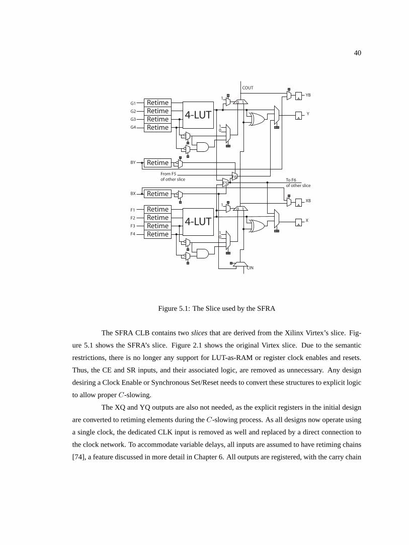
40
4-LUTRetimeRetimeRetimeRetime 1
0
10 1
4-LUTRetimeRetimeRetimeRetime 1
0
10 1
Retime
Retime
F5F6
From F5of other slice To F6
of other slice
G1
G2
G3
G4
BY
F1
F2
F3
F4
BX
YB
Y
XB
X
COUT
CIN
Figure 5.1: The Slice used by the SFRA
The SFRA CLB contains twoslicesthat are derived from the Xilinx Virtex’s slice. Fig-
ure 5.1 shows the SFRA’s slice. Figure 2.1 shows the original Virtex slice. Due to the semantic
restrictions, there is no longer any support for LUT-as-RAM or register clock enables and resets.
Thus, the CE and SR inputs, and their associated logic, are removed as unnecessary. Any design
desiring a Clock Enable or Synchronous Set/Reset needs to convert these structures to explicit logic
to allow properC-slowing.
The XQ and YQ outputs are also not needed, as the explicit registers in the initial design
are converted to retiming elements during theC-slowing process. As all designs now operate using
a single clock, the dedicated CLK input is removed as well and replaced by a direct connection to
the clock network. To accommodate variable delays, all inputs are assumed to have retiming chains
[74], a feature discussed in more detail in Chapter 6. All outputs are registered, with the carry chain
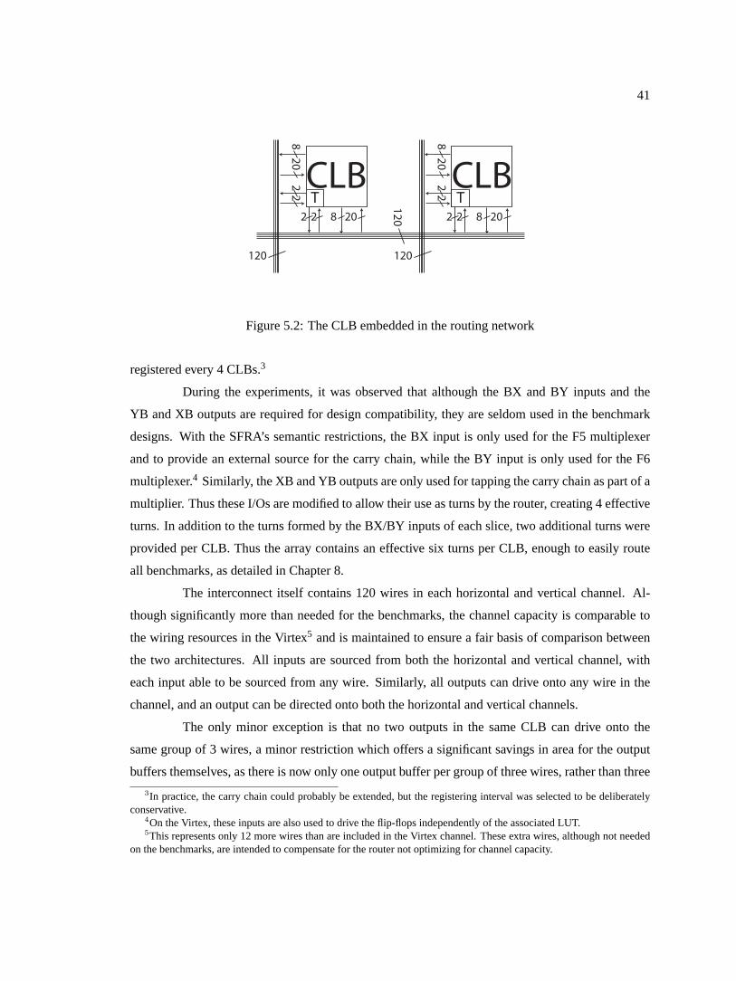
41
120
2 2 208
22
208
CLBT
120
2 2 208
22
208
CLBT120
Figure 5.2: The CLB embedded in the routing network
registered every 4 CLBs.3
During the experiments, it was observed that although the BX and BY inputs and the
YB and XB outputs are required for design compatibility, they are seldom used in the benchmark
designs. With the SFRA’s semantic restrictions, the BX input is only used for the F5 multiplexer
and to provide an external source for the carry chain, while the BY input is only used for the F6
multiplexer.4 Similarly, the XB and YB outputs are only used for tapping the carry chain as part of a
multiplier. Thus these I/Os are modified to allow their use as turns by the router, creating 4 effective
turns. In addition to the turns formed by the BX/BY inputs of each slice, two additional turns were
provided per CLB. Thus the array contains an effective six turns per CLB, enough to easily route
all benchmarks, as detailed in Chapter 8.
The interconnect itself contains 120 wires in each horizontal and vertical channel. Al-
though significantly more than needed for the benchmarks, the channel capacity is comparable to
the wiring resources in the Virtex5 and is maintained to ensure a fair basis of comparison between
the two architectures. All inputs are sourced from both the horizontal and vertical channel, with
each input able to be sourced from any wire. Similarly, all outputs can drive onto any wire in the
channel, and an output can be directed onto both the horizontal and vertical channels.
The only minor exception is that no two outputs in the same CLB can drive onto the
same group of 3 wires, a minor restriction which offers a significant savings in area for the output
buffers themselves, as there is now only one output buffer per group of three wires, rather than three
3In practice, the carry chain could probably be extended, but the registering interval was selected to be deliberatelyconservative.
4On the Virtex, these inputs are also used to drive the flip-flops independently of the associated LUT.5This represents only 12 more wires than are included in the Virtex channel. These extra wires, although not needed
on the benchmarks, are intended to compensate for the router not optimizing for channel capacity.
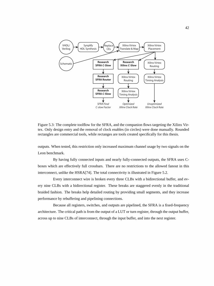
42
SynplifyHDL Synthesis
Schematic
VHDL/Verilog
Xilinx VirtexTranslate & Map
ReplaceCEs
Xilinx VirtexPlacement
ResearchXilinx C-Slow
Xilinx VirtexRouting
Xilinx VirtexTiming Analysis
UnoptimizedXilinx Clock Rate
ResearchSFRA C-Slow
ResearchSFRA Router
Xilinx VirtexRouting
Xilinx VirtexTiming Analysis
OptimizedXilinx Clock Rate
ResearchSFRA C-Slow
SFRA FinalC-slow Factor
Figure 5.3: The complete toolflow for the SFRA, and the companion flows targeting the Xilinx Vir-tex. Only design entry and the removal of clock enables (in circles) were done manually. Roundedrectangles are commercial tools, while rectanges are tools created specifically for this thesis.
outputs. When tested, this restriction only increased maximum channel usage by two signals on the
Leon benchmark.
By having fully connected inputs and nearly fully-connected outputs, the SFRA uses C-
boxes which are effectively full crossbars. There are no restrictions to the allowed fanout in this
interconnect, unlike the HSRA[74]. The total connectivity is illustrated in Figure 5.2.
Every interconnect wire is broken every three CLBs with a bidirectional buffer, and ev-
ery nine CLBs with a bidirectional register. These breaks are staggered evenly in the traditional
braided fashion. The breaks help detailed routing by providing small segments, and they increase
performance by rebuffering and pipelining connections.
Because all registers, switches, and outputs are pipelined, the SFRA is a fixed-frequency
architecture. The critical path is from the output of a LUT or turn register, through the output buffer,
across up to nine CLBs of interconnect, through the input buffer, and into the next register.
43
5.2 The SFRA Toolflow
The SFRA architecture includes a complete toolflow, illustrated in Figure 5.3. This flow
uses the Xilinx tools to perform synthesis, mapping, and placement, while custom tools were created
for C-slow retiming and routing. The details of theC-slow tool are described in Chapter 13, while
the SFRA router is described in Chapter 8. The SFRA tools are written in Java.
The overall flow is tied together with a series ofperl scripts which invoke the other
tools in the flow. The initial design, after being converted to an EDIF netlist by either Synplify or
the Xilinx Foundation schematic tool, is used as the input to the toolflow. The Foundation-created
netlists can be used unchanged, while the Synplify netlists require a minor amount of hand-editing
to replace flip-flop clock-enables and resets with explicit logic.
This netlist is first passed through the Xilinx mapping tool, which maps the design to the
Xilinx CLBs. The output of the mapper is then placed using the Xilinx place and route tool. The
design is then exported in.xdl format.
.xdl is a Xilinx defined netlist format which represents the unplaced, placed, or routed
design in terms of CLBs and connections. This textual format is a translation of Xilinx’s internal
.ncd format, and Xilinx provides a tool which can convert back and forth between the formats.
The.xdl file is then read into the SFRA toolflow, which can either target the Xilinx (by
justC-slowing), or the SFRA (where the design isC-slowed and routed). The SFRA tools can also
output.xdl , allowing designs to be reprocessed by the Xilinx tools.
Thus the complete flow has three options. The first uses just the conventional Xilinx
routing and timing analysis, providing a baseline case. The second uses the custom XilinxC-
slow tool, with the results then passed back to the Xilinx tools for routing and timing analysis.
Thus Xilinx designs can be more finely pipelined, improving their performance. The final option,
targeting the SFRA, routes and retimes the design.
Thus the complete toolflow can not only route designs for the SFRA, but supports a com-
prehensive set of comparisons with the Xilinx Virtex. The same design, with identical placement,
can target the Virtex with and without the benefits ofC-slowing, or it can target the SFRA, allowing
direct comparisons between the two architectures in terms of design latency, throughput, through-
put/area, and toolflow time, used in Chapter 14 to provide a comprehensive comparison between the
SFRA and the Xilinx Virtex.

44
5.3 Summary
This chapter introduces the SFRA’s detailed architecture and reviews the toolflow. The
SFRA is placement and design compatible with the Virtex while offering faster routing and fixed-
frequency operation.
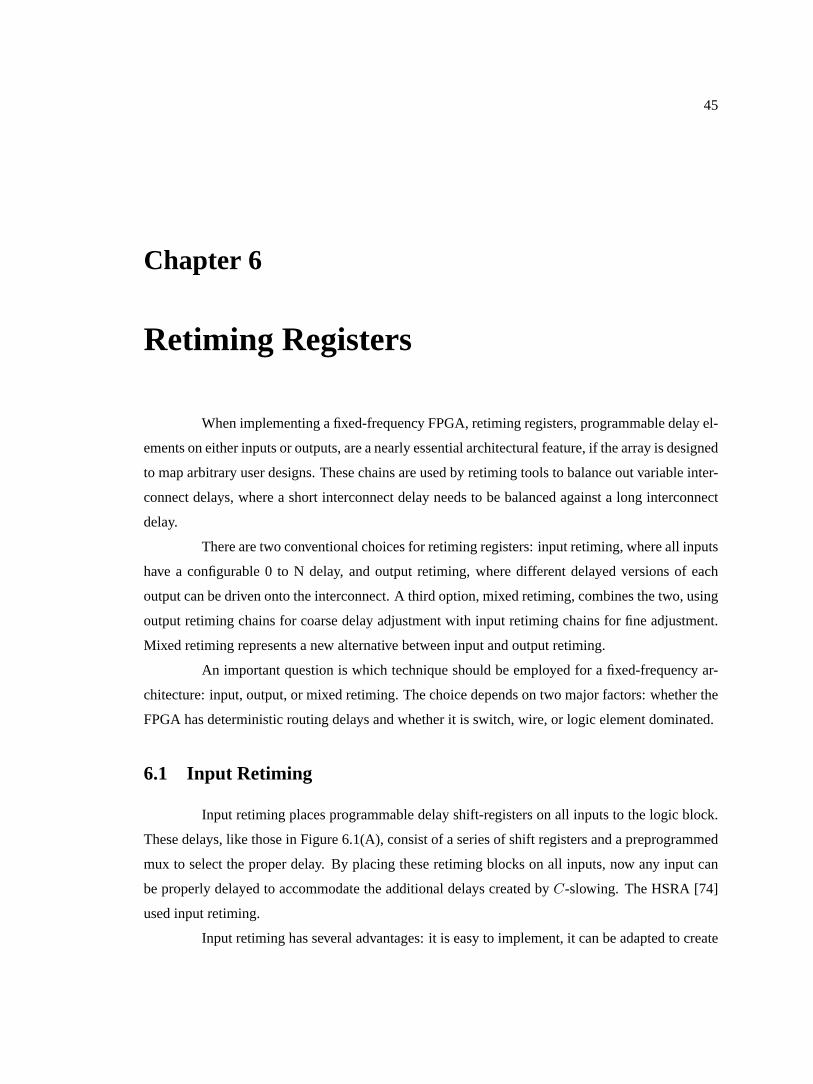
45
Chapter 6
Retiming Registers
When implementing a fixed-frequency FPGA, retiming registers, programmable delay el-
ements on either inputs or outputs, are a nearly essential architectural feature, if the array is designed
to map arbitrary user designs. These chains are used by retiming tools to balance out variable inter-
connect delays, where a short interconnect delay needs to be balanced against a long interconnect
delay.
There are two conventional choices for retiming registers: input retiming, where all inputs
have a configurable 0 to N delay, and output retiming, where different delayed versions of each
output can be driven onto the interconnect. A third option, mixed retiming, combines the two, using
output retiming chains for coarse delay adjustment with input retiming chains for fine adjustment.
Mixed retiming represents a new alternative between input and output retiming.
An important question is which technique should be employed for a fixed-frequency ar-
chitecture: input, output, or mixed retiming. The choice depends on two major factors: whether the
FPGA has deterministic routing delays and whether it is switch, wire, or logic element dominated.
6.1 Input Retiming
Input retiming places programmable delay shift-registers on all inputs to the logic block.
These delays, like those in Figure 6.1(A), consist of a series of shift registers and a preprogrammed
mux to select the proper delay. By placing these retiming blocks on all inputs, now any input can
be properly delayed to accommodate the additional delays created byC-slowing. The HSRA [74]
used input retiming.
Input retiming has several advantages: it is easy to implement, it can be adapted to create

46
LE
I0
I1
I2
(A) (B)
Figure 6.1: (A) The conceptual structure of input retiming registers. Each input has a programmableshift register on the input. (B) The typical implementation of such shift-registers. Only a single 2-1mux delay is added to the critical path driven by the retiming chain.
longer delay chains out of otherwise unused inputs, and it can easily perform retiming after routing.
The major disadvantage is that input retiming requires more retiming registers.
The common implementation of input retiming, as shown in Figure 6.1(B) is straightfor-
ward. Apart from the CLK→Q time, the only additional delay on the inputs is a single 2-1 MUX.1
For K-deep retiming, input retiming requiresO(K) registers, but onlyO(lg(K)) 2-1 muxes and
configuration bits for each retiming chain. If input retiming needs to create even longer delay chains
out of otherwise unused inputs, an additional mux can be used to select whether to source the chain
from the external input or the output of the previous retiming chain.
This allows input retiming to easily chain to produce larger delays, either when a single
LUT input is not used or when an otherwise unused LE is configured to create a long retiming delay.
Output retiming, since there are far fewer outputs to blocks when compared to inputs, can’t create
these long delay chains as easily.
The biggest problem with input retiming is simply the number of registers required. If
there areI inputs andO outputs, and retiming chains areK deep, input retiming requiresKI/O
more registers when compared with output retiming.
6.2 Output Retiming
Output retiming places the retiming resources on the output instead of the input. Instead
of each input having a programmable delay chain, various delayed versions can be routed onto
the interconnect. This uses substantially fewer registers when compared with input retiming, but
1A slight restructuring will place this mux delay on the output.
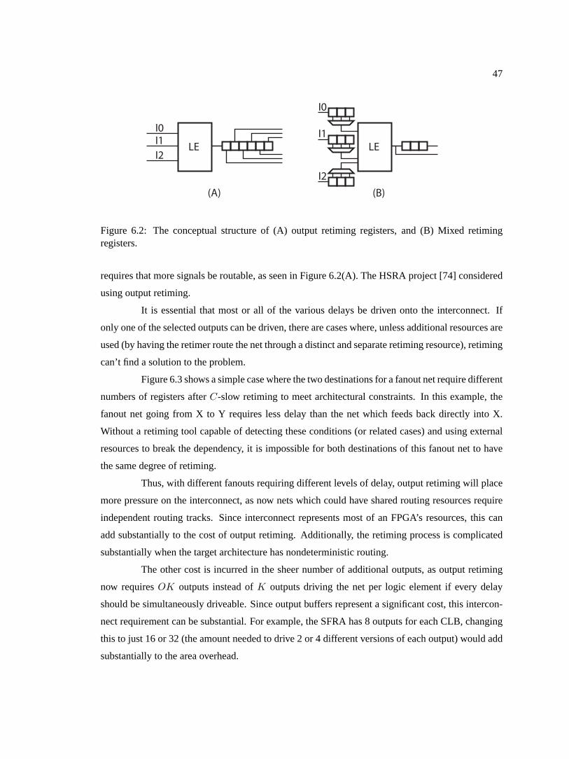
47
I0
I1
I2
(A) (B)
LELE
I0I1I2
Figure 6.2: The conceptual structure of (A) output retiming registers, and (B) Mixed retimingregisters.
requires that more signals be routable, as seen in Figure 6.2(A). The HSRA project [74] considered
using output retiming.
It is essential that most or all of the various delays be driven onto the interconnect. If
only one of the selected outputs can be driven, there are cases where, unless additional resources are
used (by having the retimer route the net through a distinct and separate retiming resource), retiming
can’t find a solution to the problem.
Figure 6.3 shows a simple case where the two destinations for a fanout net require different
numbers of registers afterC-slow retiming to meet architectural constraints. In this example, the
fanout net going from X to Y requires less delay than the net which feeds back directly into X.
Without a retiming tool capable of detecting these conditions (or related cases) and using external
resources to break the dependency, it is impossible for both destinations of this fanout net to have
the same degree of retiming.
Thus, with different fanouts requiring different levels of delay, output retiming will place
more pressure on the interconnect, as now nets which could have shared routing resources require
independent routing tracks. Since interconnect represents most of an FPGA’s resources, this can
add substantially to the cost of output retiming. Additionally, the retiming process is complicated
substantially when the target architecture has nondeterministic routing.
The other cost is incurred in the sheer number of additional outputs, as output retiming
now requiresOK outputs instead ofK outputs driving the net per logic element if every delay
should be simultaneously driveable. Since output buffers represent a significant cost, this intercon-
nect requirement can be substantial. For example, the SFRA has 8 outputs for each CLB, changing
this to just 16 or 32 (the amount needed to drive 2 or 4 different versions of each output) would add
substantially to the area overhead.

48
(A) (C)
1
1
0X Y
1
2
1X Y
(B)
X Y* *
Figure 6.3: A case where the output of X’s two destinations will always have different delays. (A)shows the initial design beforeC-slowing. (B) marks with an astrerix (*) the two places whichrequire a register to meet a set of constraints. (C) shows the design afterC-slowing. X’s singleoutput must have two different delays, a single cycle for the input to Y, and a two cycle delay forthe feedback loop.
6.3 Mixed Retiming
A logical division is to provide for mixed retiming. In this case, each input has a pro-
grammable0 to K/2 delay, with the outputs for both1 and K/2 routed onto the interconnect.
Thus any delay from1 to K can be produced by combining the proper output with the input delay.
Figure 6.2(B) demonstrates the structure of mixed-retiming. This option has not previously been
considered.
Mixed retiming’s goal is to combine the benefits of output retiming (fewer retiming reg-
isters) with the benefits of input retiming (lower interconnect requirements). Unfortunately, as
discussed in the next section, mixed retiming shares many of the limitations of output retiming,
including considerably more output signals which need to be routable and a need for deterministic
routing delays for retiming to work before routing.
6.4 Deterministic Routing Delays
If a fixed-frequency FPGA has deterministic routing delays, it is far easier to utilize mixed
or output retiming. In such FPGAs all delays can be accurately accounted and retiming performed
before routing the design. Thus, in the case of mixed or output retiming, there is no problem
in ensuring that the correctly delayed output is routed, considerably simplifying the routing and
retiming problem.
The situation is significantly more complex in the case where interconnect delays can’t

49
be computed ahead of routing. In this case, there appear to be two possible strategies to conduct
successful retiming: either treat all nets as point to point or force retiming to attempt to group fanout
nets together.
The first option is straightforward: treat every net as a point to point net, breaking up
fanout as necessary. Then, after routing the design, perform retiming and then select the proper
output for each delay. This technique allows a nondeterministic array to utilize mixed or output
retiming, because it defers the decision on which particular delayed version to route until after
retiming is complete.
There are two limitations of this approach: all the different delay possibilities must be
interchangeable, and it may require significantly more routing resources for high fanout nets.
The first cost is obvious: in order to postpone the decision on which signal to route until
after retiming, it is necessary that the different possibilities be interchangeable. In practice, this
restriction should not be substantial, as all the possible delays still need to be routed, and there does
not appear to be substantial benefits to utilizing different routing resources for the different delays
on the same output.
The second, the need to route fanout independently, is considerably more costly. Unless
it is known before routing that it is possible to share destinations, the router will need to treat all
possible destinations as separate signals. This greatly increases the number of signals to route and
has the effect of causing fanouts to occur earlier in the network, limiting the ability for multiple
destinations to share wires or turns. Without allowing fanout to share turns, the LEON benchmark
requires 7 turns to route sucesfully, but only requires 5 turns to route when fanouts can share turns.2
The other option requires that retiming treat all fanout nets as requiring the same number
of output delays, in addition to any interconnect delay. But, as seen in the example of Figure 6.3,
there are cases where this strategy obviously fails. Thus the retiming tool must first search for all
feedback loops with internal fanout and ensure that the fanout is treated properly.
Even if the retiming tool completes this transformation and uses it to guide routing, the
resulting design will probably require more latency, as now many nets will have more registers than
are strictly required due to the shared output retiming.
Thus, unless the FPGA has deterministic routing delays, it appears best to use input re-
timing instead of mixed or output retiming, to reduce the complexity and routing pressure and to
2This experiment was accomplished by setting the fanout threshold, the number of fanouts required before a net isrouted using the fanout-technique, to an arbitrarily high amount. This change forces all connections to use their own turnsrather than sharing resources.

50
prevent excessive design latency from being introduced during the retiming process. Since the
SFRA architecture does not have deterministic routing, input retiming is the superior solution.
6.5 Area Costs
Even for an FPGA with deterministic routing, the area costs may favor input over mixed
and output retiming. There are several cases of FPGAs: Logic cell dominated, wire dominated,
switch dominated, or interconnect dominated.
In a logic-cell dominated FPGA, such as the Xilinx 6200 [81], most of the resources
are spent on the logic cell instead of the interconnect. Such cases generally occur in routing-poor
FPGAs, which are no longer commercially viable. In these FPGAs, reducing the cost of retiming
registers is essential. Input retiming will requireKI registers, while output retiming only needs
KO registers, but requires an additional(K − 1)O outputs. Output retiming is area favorable only
when the(K − 1)O additional output buffers require less area than theKI input registers.
Mixed retiming is probably best suited, as now there are(K/2)I input registers,(K/2)O
output registers, and onlyO additional output buffers driving onto the interconnect. Thus it is more
likely that the additional output buffers will not increase the cost when compared to the savings on
input retiming resources.
For an interconnect dominated FPGA, either wire, switch, or a balanced cost, output
retiming is clearly not favorable. Even in the ideal case, the additional routing requirements for high
fanout nets are substantial, as some nets will need allK outputs to be routed and many nets will
require two or more outputs to be routed. Even just a 10% increase in overall channel requirements is
substantial if routing resources dominate the FPGA’s cost. Additionally, for such arrays, the output
buffer costs will probably dominate, except in the case of very large values ofK, simply because
every output buffer contains numerous controllable switches that, depending on the architecture,
may not be encodable.
Mixed retiming may still be of benefit, however. In the mixed retiming case, the maximum
interconnect requirement is multiplied by 2 in the worst-case fanout, but in practice it should be
substantially less. Yet it still requires a 2x increase in the output buffers themselves. In this case,
it is necessary to balance the interconnect pressure and output buffer size against the savings in
retiming registers to determine if it is preferable to use mixed retiming.
Currently, mixed retiming or input retiming appears the optimum choice for fixed fre-
quency arrays with deterministic routing, depending on the balance between interconnect pressure

51
and area costs. For fixed-frequency arrays with nondeterministic routing, it is best to use input
retiming because of the simpler tool problem.
6.6 Retiming and the SFRA
Since the output buffers are a substantial cost for the SFRA, and the routing delays are
nondeterministic, output retiming is clearly infeasible. Even mixed retiming is unattractive, as
increasing the number of output buffers in each channel from 10 to 18 would seriously impact the
resulting area. This is especially noticeable when the SFRA layout contains a 54,000µm2 gap for
the CLB and retiming registers: a space equal to the entire Virtex CLB and associated interconnect.
Even large input retiming chains can be implemented without impacting the resulting area. Thus
output retiming or mixed retiming are clearly unsuitable for use with the SFRA.
6.7 Summary
This chapter reviewed the architecture of retiming registers, introduced a new option
(mixed retiming) and analyzed where one of the three various alternatives: input, output, or mixed
retiming is most appropriate. For the SFRA, input retiming is the clearly superior choice.
52
Chapter 7
The Layout of the SFRA
The layout for the critical circuits of the SFRA was constructed using Cadence, targeting
ST Microelectronic .18µm, 1.8 volt, 6 layer metal process. The process is comparable, but not
identical, to the .18µm TSMC and/or IBM processes used by Xilinx for the Virtex-E family of
FPGAs. The layout includes the interconnect drivers, input, and output buffers for the SFRA, as it
is these circuits which define both the critical path and the silicon cost for the SFRA.
The critical path is from the output register, through the output buffer, onto the general
interconnect, a traversal of 9 CLBs in distance, and through an input buffer and to the input register.
The interconnect registers themselves are not on the critical path, as the resulting signal will travel,
at most, the same 9 CLBs but will not pass through an input or output buffer.
Likewise, the critical area is defined by the input, interconnect, and output buffers and
their associated configuration bits. This is because the SFRA’s C-boxes are effectively full crossbars,
with each CLB containing 22 inputs and 10 outputs connecting to an interconnect channel with 120
wires. This layout is not intended to be a complete design, but to create justified timing and area
estimates for further comparison.1
7.1 Layout Strategy
The layout uses 4 layers of interconnect for the bulk of the communication channel, leav-
ing layers 5 and 6 free to bridge signals over the active switchpoints, provide for clock distribution,
and additional power and ground distribution, as seen in Figure 7.1. Metal 1 is used for local signals
1Although the critical path and area are defined by the interconnect, most of the design complexity would be in thelogic cell and verification.

53
M1: Power/GndM3: Power/Gnd Local interconnectM4: Power/Gnd General interconnect Bitlines
M2: Power/Gnd Data in/out Wordlines
3 Signals2 Bitlines
Power/Gnd3.84 µm
BasicTile
Figure 7.1: The basic layer assigments. The tiles all are designed to tile along the top and bottom,so the power and ground connections are all routed along the tile boundries. Likewise, the overalltiles are designed to tile on the left and right sides as well. To create the vertical channel, the tilesare rotated 90 degrees. Metal 5 and 6 are reserved for routing independant signals over the tiles.
and to provide power and ground connections parallel to the communication channel. Metal 2 is
used for perpendicular signals, including the SRAM wordlines, and the inputs and outputs to the
I/O buffers. Metal 3 provides local versions of the interconnect signals as well as power and ground,
running parallel and underneath to the communication channel. Metal 4 is used for the main inter-
connect channel, with a power, ground, three signals, and two bitlines. Configurations are loaded
from the bitlines. To create the vertical channel, the design is simply rotated 90 degrees.
It is metal 4 which determines the tile pitch. The pieces tile top-to-top and bottom-to-
bottom, so the power and ground supplies, transistor connections, and well contacts are shared
between the tiles. Each metal 4 tile includes power and ground wires (which are shared along the
tile boundary), two bitlines (a signal and its complement) and three communication wires. Since
there are 120 signals in each communication channel it requires 40 vertical tiles to form the com-
plete channel. The layout is staggered so that communication signals are only adjacent to bitlines
or power/ground connections, not other communication lines, limiting crosstalk. Likewise, the
metal 3 signals underneath the channel are always either floating, nonexistent, or contain a normal
(noninverted) copy of the metal 4 signal. Thus a communication line is never coupled to other
communication lines, only copies of itself.
If the channel did not include the bitlines for the configuration, it could be reduced but

54
CLBOutput CLB
Input
Figure 7.2: The basic circits of the SFRA’s interconnect. Each output is driven onto a series of 40tristates, with each tristate driving an output wire. Every output tristate in the same row drives ontothe same output wire. The output wires can then be driven onto one of three different interconnectwires. The general interconnect wires are broken and rebuffered every 3 CLBs.
only by a limited degree as the minimum vertical pitch for the SRAM cell itself is only slightly
smaller. If the channel pitch instead used four communication wires and one bitline, the resulting
C-boxes would be significantly longer and therefore not able to tile as effectively, even though the
switch area itself could be substantially reduced. Likewise, this would be slower as now there would
be cross-coupling between active signaling lines.
Power and ground wires occur on all of the first four layers of metal. The metal 1, 3, and
4 power and ground lines are vertically stacked, with vias continuously connecting the metal 3 and
4 lines. Every tile has a via stack connecting the metal 1 power and ground connections to their
metal 2 and metal 3 counterparts. Every tile also contains at least one well or body connection.
Figure 7.2 shows the basic strategy used in the SFRA’s channel. Each output drives a
inverter which is used to source an entire column of tristates. At most, only one tristate on each wire
is active, driving a local output wire in metal 3. This output wire can then be driven onto one of
three interconnect wires by an interconnect buffer. Thus the output buffer is not quite a full crossbar,
as no two outputs in the same CLB can drive into the same bundle of three wires. This introduces
two levels of somewhat unbalanced heirarchy, but adding a more balanced heirarchy (so that the
primary driver sees a lower amount of fanout) would have added significant area.
The interconnect wires themselves are broken and rebuffered with tristates every 3 CLBs

55
and registered every 9 CLBs. This uses the conventional braiding pattern, where 1/3rd of the wires
are broken at each CLB. The interconnect buffers are noninverting, as this balances the critical path.
For inputs, another buffer is used to drive the signal onto a local interconnect segment.
This is a noninverting buffer, as the output wire is capacitively coupled to the interconnect wire
above it. This isolates the input buffer’s capacitive load from the main communication channel. The
local wire then drives a series of tristate buffers, with each tristate’s output being driven upwards to
a final input mux which selects between one of the six possibilities.
The result is a hierarchical network. The output tristates only drive a local signal, which
is then rebuffered onto the general interconnect. Likewise, the input buffers are similarly isolated
from the interconnect, while the main interconnect only sees a small amount of capacitive load, as
no inputs are directly connected to the interconnect wires. The final input mux adds yet another
level of hierarchy, reducing the load on the input buffer’s tristates.
This hierarchy also enables some natural configuration encoding. Each line of output
buffer needs 40 bits of SRAM, rather than 120 if the wires were directly driven. There are an addi-
tional 120 bits used for the tristates which connect the output wires to the interconnect wires. The
same encoding applies to the input buffers, as only 40 bits need to be stored in the channel. Saving
configuration bits themselves is not very significant: the advantage lies in reducing the number of
SRAM cells needed to control the interconnect. Likewise, further encoding configuration bits is not
generally effective, as decoders would require more area than the SRAM cells they replace.
7.1.1 SRAM Cell
The SRAM cell (shown in Figure 7.3), used to control numerous switches in the channel,
is slightly larger than optimal in order to be more usable. The vertical size could be shrunk slightly,
but the size needs to match the pitch of the communication channel. Additionally, both the state and
the complement need to be accessible to control the adjacent switchpoint, a requirement which adds
substantially to the resulting area.
In order to make the control signals available, the layout is slightly convoluted as the top
half of one cross-coupled inverter is located directly over the other inverters bottom half. This way,
the two poly connections can be used to read both the data and complement out of the SRAM cell
and are used as select lines to control tristates.
The select lines are the only signals routed as polysilicon rather than metal. The actual
configuration seldom changes, thus routing the outputs in polysilicon save area as these link directly

56
Sel
Sel
BitlineBitline
Wordline
Figure 7.3: The SRAM cell layout, and the corresponding circuit. Only the active, poly, N-wells,metal 1, and metal 2 layers are shown. Unlike a normal SRAM cell, the top is twisted to enable theselect lines (in polysilicon) to directly control an associated tristate. The SRAM can be tiled on thetop, left side, and bottom, with appropriately mirrored copies.
to the tristate gates. This SRAM cell tiles on only three sides: top, left, and bottom, as the right side
exports the control signals to the tristates used for the rest of the design. When tiled, the power and
ground connections and well contacts are shared between adjacent cells. The SRAM cell is 3.84
µm high and 3.1µm wide, or 1.5 kλ2 in area.
Although using a bitline/wordline structure (rather than a shift chain) to load configura-
tions requires more interconnect, the actual cost is relatively low. Removing a wire from the metal
4 channel would allow the SRAM cell to be reduced by only about .4 microns, given the twisted-
structure employed to export both the value and the complement to the associated tristate. Similarly,
removing one of the bitlines and replacing it with another interconnect signal, although resulting in
a lower area for the C-boxes, results in a larger total area as the horizontal and vertical channels
can’t be tiled as efficiently.
Similarly, although only a single SRAM in an individual input or output buffer is ever on,
using SRAMs instead of decoders saves considerable circuit area. A 6-bit input decoder requires
at least twelve transistors and twelve wires perpendicular to the channel. Since the SRAM cell
is only 6 transistors, and the width is significantly narrower than twelve metal 2 wires, it is more
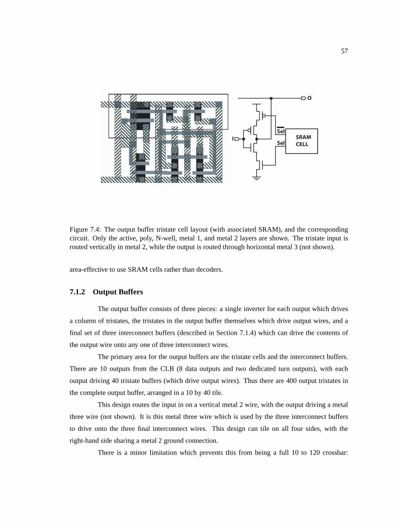
57
SRAMCELL
ISel
Sel
O
Figure 7.4: The output buffer tristate cell layout (with associated SRAM), and the correspondingcircuit. Only the active, poly, N-well, metal 1, and metal 2 layers are shown. The tristate input isrouted vertically in metal 2, while the output is routed through horizontal metal 3 (not shown).
area-effective to use SRAM cells rather than decoders.
7.1.2 Output Buffers
The output buffer consists of three pieces: a single inverter for each output which drives
a column of tristates, the tristates in the output buffer themselves which drive output wires, and a
final set of three interconnect buffers (described in Section 7.1.4) which can drive the contents of
the output wire onto any one of three interconnect wires.
The primary area for the output buffers are the tristate cells and the interconnect buffers.
There are 10 outputs from the CLB (8 data outputs and two dedicated turn outputs), with each
output driving 40 tristate buffers (which drive output wires). Thus there are 400 output tristates in
the complete output buffer, arranged in a 10 by 40 tile.
This design routes the input in on a vertical metal 2 wire, with the output driving a metal
three wire (not shown). It is this metal three wire which is used by the three interconnect buffers
to drive onto the three final interconnect wires. This design can tile on all four sides, with the
right-hand side sharing a metal 2 ground connection.
There is a minor limitation which prevents this from being a full 10 to 120 crossbar:
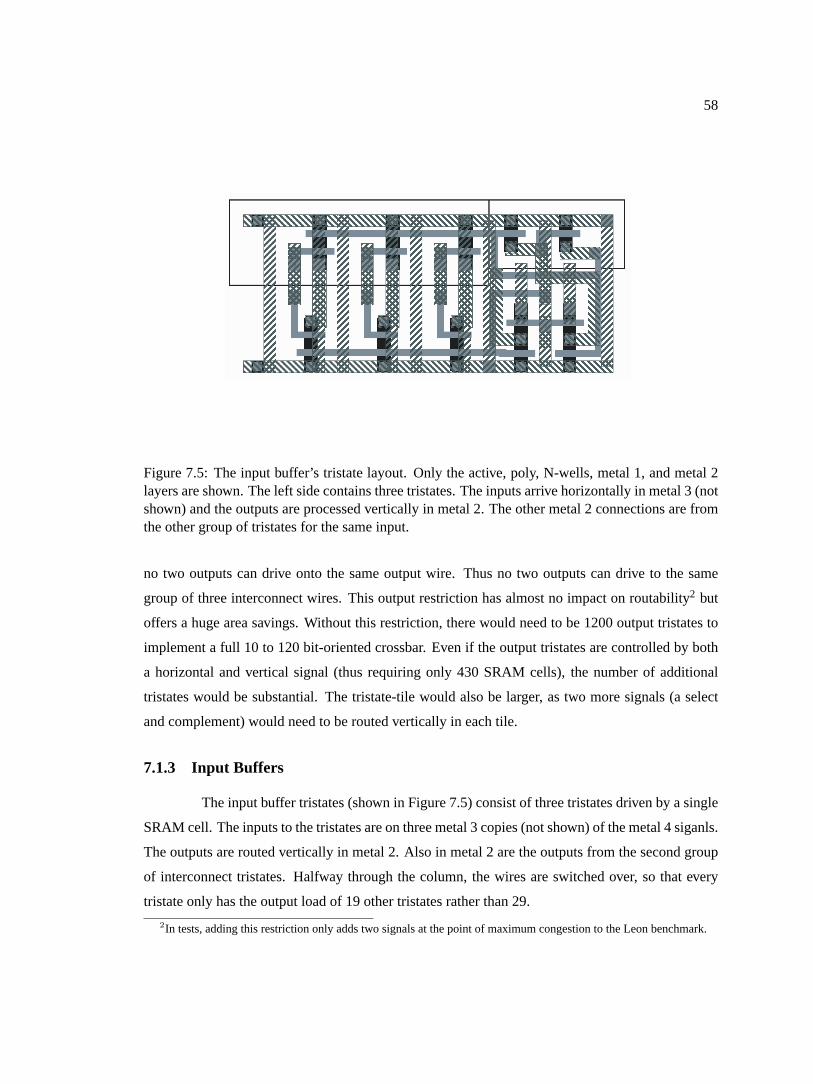
58
Figure 7.5: The input buffer’s tristate layout. Only the active, poly, N-wells, metal 1, and metal 2layers are shown. The left side contains three tristates. The inputs arrive horizontally in metal 3 (notshown) and the outputs are processed vertically in metal 2. The other metal 2 connections are fromthe other group of tristates for the same input.
no two outputs can drive onto the same output wire. Thus no two outputs can drive to the same
group of three interconnect wires. This output restriction has almost no impact on routability2 but
offers a huge area savings. Without this restriction, there would need to be 1200 output tristates to
implement a full 10 to 120 bit-oriented crossbar. Even if the output tristates are controlled by both
a horizontal and vertical signal (thus requiring only 430 SRAM cells), the number of additional
tristates would be substantial. The tristate-tile would also be larger, as two more signals (a select
and complement) would need to be routed vertically in each tile.
7.1.3 Input Buffers
The input buffer tristates (shown in Figure 7.5) consist of three tristates driven by a single
SRAM cell. The inputs to the tristates are on three metal 3 copies (not shown) of the metal 4 siganls.
The outputs are routed vertically in metal 2. Also in metal 2 are the outputs from the second group
of interconnect tristates. Halfway through the column, the wires are switched over, so that every
tristate only has the output load of 19 other tristates rather than 29.
2In tests, adding this restriction only adds two signals at the point of maximum congestion to the Leon benchmark.

59
SRAMCELL
Sel
SelI O
Figure 7.6: The interconnect buffer layout with associated SRAM cell, and the corresponding circuitimplemented. Only the active, poly, N-wells, metal 1, and metal 2 layers are shown. Both input andoutput occur on either metal 3 or metal 4, with the input driving the small inverter used to drives thelarge tristate.
At the top of the interconnect buffer is a 6-to-1 mux which selects between one of the six
signals. This structure is used to add an additional layer of hierarchy and to save bits. The bits for
this mux are not located in the interconnect channel, thus the area is not critical as they fit in the
large gap for the CLB. This allows the interconnect buffers themselves to only contain 40 bits per
input, or 880 bits total. It also adds a layer of hierarchy which allows for faster inputs. Otherwise, if
all tristates for an input connected onto a single line, each tristate would see the parasitic output-load
from 119 other tristates.
7.1.4 Interconnect Buffers
The interconnect buffers, shown in Figure 7.6, are used in three separate locations in the
SFRA’s channel: to break and rebuffer the general interconnect, to drive signals from the output-
buffer local interconnect onto the general interconnect, and to drive signals from the general inter-
connect to the ibuf-local interconnect.
These are noninverting tristate buffers rather than inverting tristates. This first serves to
reduce the load on the interconnect, as the inputs are minimum-sized. For the output and input

60
ApproximateHSRA area for
four LUTs
VirtexCLBTile
Ibu
fs
Ob
ufs
Ibufs
Obufs
SFRACLBGap
100µm
Figure 7.7: The SFRA’s CLB tile, and the comparative size of the Xilinx Virtex-E tile and a scaledHSRA tile containing 4 LUTs. The portions of the SFRA’s tile shown in gray were layed out to de-termine the critical area and path of the design. The HSRA tile is based on an area of approximately4 Mλ2 per LUT, scaled to a .18µm process.
buffers, the use of noninverting buffers speeds communication because the input and outputs are
capacitively coupled between the metal 4 and metal 3 signals. On the general interconnect, using
noninverting buffers insures that the slow portion of the output buffer (a low to high transition)
matches the fast portion of the input buffer in all cases.
7.2 Overall Area
The resulting area (shown in Figure 7.7) is approximately 160,000µm2. This is roughly
3.9x larger than the Xilinx Virtex E’s CLB tile (with interconnect), but only 1.5x larger than the
HSRA’s tile. The gap in the tile for the logic cell is sufficient to accomodite the entire Virtex E CLB
tile, suggesting that the SFRA’s CLB plus retiming registers could easily fit in this space.
Although substantial, the area increase is understandable given that the SFRA has much
richer connectivity on the interconnect, as the C-boxes are full crossbars compared to the highly
restrictive topology of the Virtex. Additionally, the SFRA’s pipelined interconnect enables a much
higher throughput operation, which compensates for this increased area cost. This interconnect
structure is also substantially easier to route as Chapter 14 demonstrates.
Although the SFRA is only slightly larger than the HSRA (a comparable fixed-frequency
architecture), the SFRA has a vastly richer interconnect, having vastly more wires and much richer
61
connectivity. The HSRA’s base channels were far narrower than the SFRAs and the interconnect
itself is substantially more restricted. At each tree junction, a signal on one branch could only be
routed to the corresponding wire on another branch or up the tree on either one or two wires.
The use of full crossbars for input and output buffers implies that corner-turn networks
are better suited for coarse-grained FPGAs. Crossbars which interconnect 8, 16, or 32 bit words
require substantially fewer switches and configuration bits per wire, leading to wire dominated,
rather than switch dominated structures. As there have been no commercially successful word-
oriented FPGAs with publically-manipulatable toolflows, the SFRA needed to utilize a comparable
bit-oriented structure (the Xilinx Virtex) rather than a word-oriented design.
7.3 Timing Results
Timing was estimated by writing a small C program which created a final netlist with the
appropriate parasitics which was then simulated using the Cadence Spectre circuit simulator. A pro-
gram was used because this allowed for substantially faster experimentation, as different transistor
sizes could be input and immediately evaluated.
The critical path begins at an output register, passes through the output buffer and onto the
general interconnect. Once on the interconnect, the signal passes next to 9 CLBs. At the 9th CLB,
the signal passes through the input buffer and through the final input mux to where it is registered.
All but the registers were directly simulated.
Traversing the output buffer from the register output to the general interconnect requires
approximately.8 ns. The 9 CLBs of general interconnect only require about.4 ns, as the capacitive
load on the wires is very low (only 5 input loads and 5 output loads ever 3 CLBs). Finally, the input
buffer requires another1.1 ns. The total path requires approximately2.3 ns for a signal to traverse.
Budgeting an additional.5 ns for flip-flop setup and clock→Q and another.5 ns for clock
skew, variation, and general margin, a clock period of3.3 ns appears more than reasonable. Thus
the SFRA appears capable of 300 MHz operation.
7.4 Summary
This chapter presents he critical circuits of the SFRA, which define both the critical path
and area (input, output, and interconnect rebuffers). These circuits were constructed in a .18µm
process. The resulting design is approximatly 3.9 times larger than the Xilinx Virtex-E, but able to

62
run at a substantially higher (300 MHz) clock rate on all designs. This layout is only slightly larger
than the HSRA’s layout, but offers a much richer and more plentiful interconnect structure. Unlike
the HSRA, the SFRA’s interconnect supports fast routing algorithms.
63
Chapter 8
Routing a Corner-Turn Interconnect
Any proposed FPGA architecture requires a toolflow to automatically map designs. Al-
though the SFRA is placement compatible with conventional FPGA designs, it presents novel rout-
ing problems.
The global routing for a corner-turn interconnect requires several passes, all of which are
polynomial time. Before routing, any connection which requires no turns is routed directly. Then
there is an approximation designed to route high-fanout nets in an efficient manner. The next step
is a comprehensive search designed to route all nets using the minimum number of turns. The next
step attempts to route designs using two turns. Finally, a last ripup-and-reroute step is employed.
Detailed routing uses channel-independent packing.
These routing algorithms are designed to minimize the number of turns required to route
a design as the turns, not the wires in the channel, are the critical resource when targeting the SFRA.
A secondary objective is to minimize the additional delays introduced by routing. No concern is
applied to minimizing channel congestion, although additional passes could be applied to reduce
the congestion in hotspots.
When actually routing for the SFRA architecture (described in Chapter 5), the process
first begins with a fixed frequency retiming pass, then a routing pass, and a final retiming pass.
The initial retiming provides priority to the critical path in an attempt to minimize the number of
additional delays required. This is accomplished in a single Java-based tool which reads designs as
.xdl .
64
8.1 Interaction with Retiming
Retiming, discussed in detail in Chapter 10, automatically balances interconnect delays
to achieve higher performance. If any given path is not on the critical path, there is no problem if
additional routing delays are incurred. But for logic on the critical path, any delays added by the
router will degrade the latency of the final design.
There are two cases where routing can add additional delays beyond the minimum. During
global routing, each additional taken turn will add one additional cycle of pipelining. The router
itself will only add at most one extra turn. Detailed routing can add delays for each channel, if the
resulting connection goes through an additional segment. Thus, the worst case: an additional turn
and 3 additional segments, will add 4 cycles of delay to a signal.
Although some signals will not be affected by these additional delays, signals on the
critical path require prioritization to prevent additional delays from accruing. Unlike a conventional
array, a bad route will not affect the clock cycle. Instead, a greater level ofC-slow retiming will
be needed to meet the array’s requirements. Thus, the penalty for a bad routing decision is lower.
However it is still of concern, if the application does not have sufficient parallelism, requiring that
some of the issue slots go unused.
In order to prioritize the critical path, an initial retiming is performed. This retiming uses
the best-case delay model, where every net is routed with a single turn, and the detailed routing
never adds unnecessary segment breaks. Thus, it serves two purposes: a measure of routing quality
and a guide for routing decisions.
This forms a mostry-reliable guide for routing decisions: any net on the critical path can
have no delay added, while any net which requires several added delays is not on the critical path.
It is possible for some noncritical nets to have no delays added during the retiming process, but
otherwise the retiming provides an accurate guide for routing decisions.
8.2 The Routing Process
The routing process requires several steps of global routing, followed by a detailed routing
pass. Global routing assigns each net to use a series of turns and channels, while detailed routing
assigns the nets to the actual wires in the channel.
Direct routing, described in Section 8.2.1, first routes all connections which can be routed
directly, without using any turns. After that, fanout routing, described in Section 8.2.2, routes all
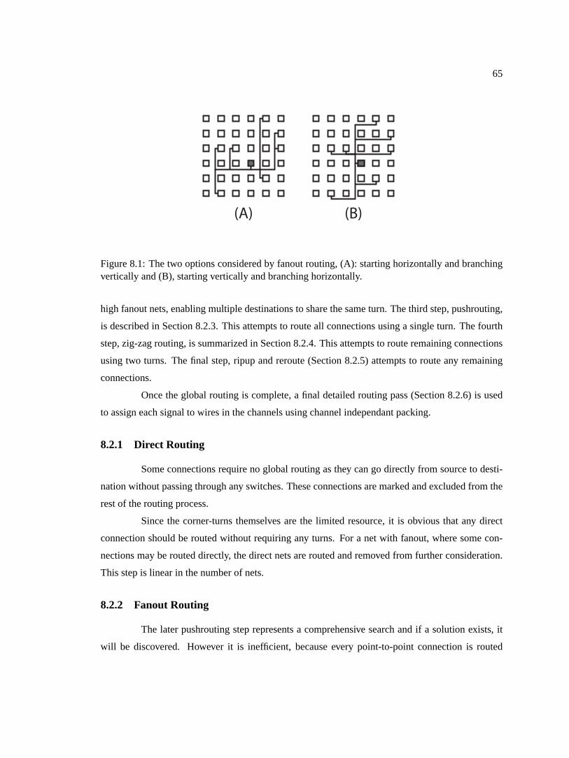
65
(A)
S
(B)
Figure 8.1: The two options considered by fanout routing, (A): starting horizontally and branchingvertically and (B), starting vertically and branching horizontally.
high fanout nets, enabling multiple destinations to share the same turn. The third step, pushrouting,
is described in Section 8.2.3. This attempts to route all connections using a single turn. The fourth
step, zig-zag routing, is summarized in Section 8.2.4. This attempts to route remaining connections
using two turns. The final step, ripup and reroute (Section 8.2.5) attempts to route any remaining
connections.
Once the global routing is complete, a final detailed routing pass (Section 8.2.6) is used
to assign each signal to wires in the channels using channel independant packing.
8.2.1 Direct Routing
Some connections require no global routing as they can go directly from source to desti-
nation without passing through any switches. These connections are marked and excluded from the
rest of the routing process.
Since the corner-turns themselves are the limited resource, it is obvious that any direct
connection should be routed without requiring any turns. For a net with fanout, where some con-
nections may be routed directly, the direct nets are routed and removed from further consideration.
This step is linear in the number of nets.
8.2.2 Fanout Routing
The later pushrouting step represents a comprehensive search and if a solution exists, it
will be discovered. However it is inefficient, because every point-to-point connection is routed
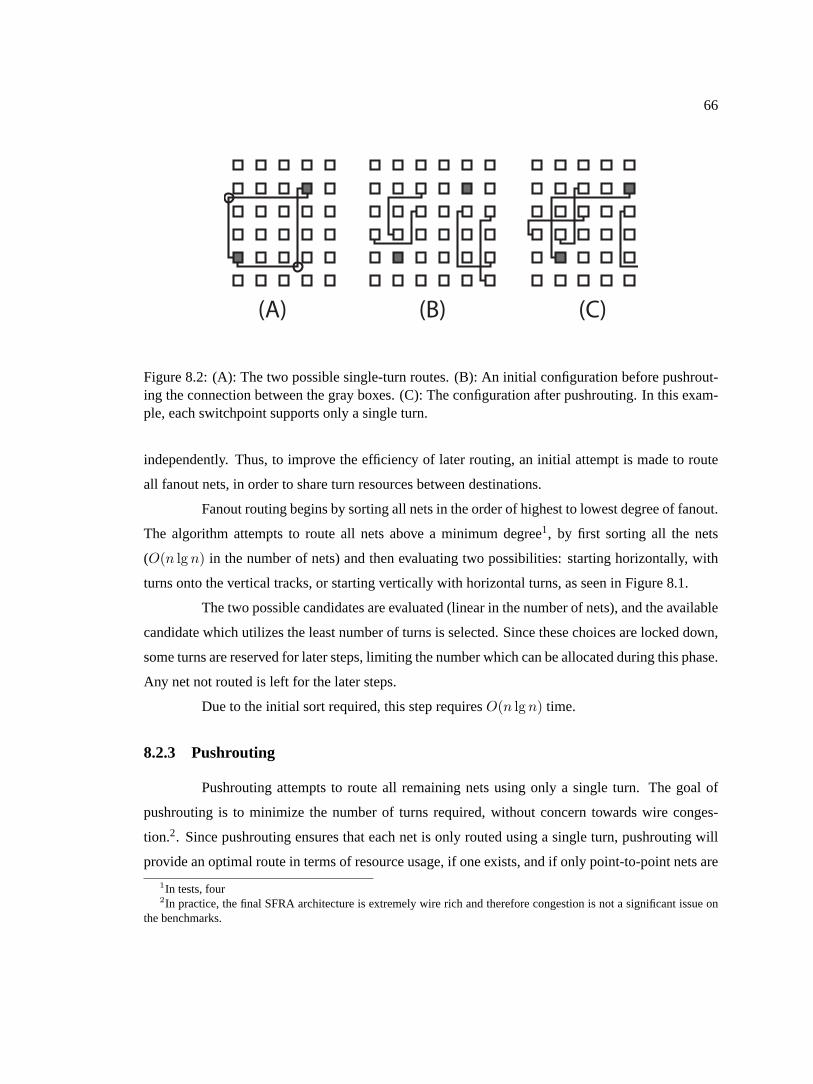
66
(A) (B) (C)
Figure 8.2: (A): The two possible single-turn routes. (B): An initial configuration before pushrout-ing the connection between the gray boxes. (C): The configuration after pushrouting. In this exam-ple, each switchpoint supports only a single turn.
independently. Thus, to improve the efficiency of later routing, an initial attempt is made to route
all fanout nets, in order to share turn resources between destinations.
Fanout routing begins by sorting all nets in the order of highest to lowest degree of fanout.
The algorithm attempts to route all nets above a minimum degree1, by first sorting all the nets
(O(n lg n) in the number of nets) and then evaluating two possibilities: starting horizontally, with
turns onto the vertical tracks, or starting vertically with horizontal turns, as seen in Figure 8.1.
The two possible candidates are evaluated (linear in the number of nets), and the available
candidate which utilizes the least number of turns is selected. Since these choices are locked down,
some turns are reserved for later steps, limiting the number which can be allocated during this phase.
Any net not routed is left for the later steps.
Due to the initial sort required, this step requiresO(n lg n) time.
8.2.3 Pushrouting
Pushrouting attempts to route all remaining nets using only a single turn. The goal of
pushrouting is to minimize the number of turns required, without concern towards wire conges-
tion.2. Since pushrouting ensures that each net is only routed using a single turn, pushrouting will
provide an optimal route in terms of resource usage, if one exists, and if only point-to-point nets are
1In tests, four2In practice, the final SFRA architecture is extremely wire rich and therefore congestion is not a significant issue on
the benchmarks.

67
considered.3
Pushrouting begins by sorting the remaining nets in terms of distance and priority. Short
nets are routed first, as there is less freedom to zig-zag route these nets later. Nets on the critical
path are preferentially routed to ensure that the minimum amount of delay is added by the router.
This sort requiresO(n lg n) time to complete.
After sorting, each net is routed by considering the two possible one-turn routes. If one
of the routes is available, it is selected for the net. If both are available, one is selected. As will be
seen in the search phase, it does not matter which choice is selected.
If neither route is free, pushrouting begins a depth-first search to determine if there exists
a series of moves which can free one of the two possible turn locations, as seen in Figure 8.2. Since
there are only two options for any given net, the one currently employed and the one it can move to,
this search is comprehensive. In the worst case, it will examine all already routed nets which may
be moved to create a route for this net. Thus, to route thekth net, it may require examining allk−1
nets which were previously routed. Thus, the worst-case running time isO(n2) for pushrouting.
If there is no fanout, and there exists a solution where all nets are routed using a single
turn, ignoring channel congestion, pushrouting will discover this route. This is due to the compre-
hensive nature of the pushroute search. Attempting to route theN th net will succeed only if either
the net can be directly routed, or if there exists a configuration of the previousN − 1 nets which
allows theN th to be routed, a configuration which is discovered by the depth first search.
8.2.4 Zig-zag (2 turn) routing
After pushrouting, all remaining unrouted nets are “zig-zag” routed. For each net, all
possible two-turn routes are examined, as seen in Figure 8.3. These routes represent minimum
distance and minimum plus one number of turns. Each net is examined to determine which possible
route is available. If one or more is available, a random route is selected and used for routing.
This phase is obviously better adapted for routing longer nets, as there is significantly
more freedom making it more likely that an available route will be discovered. Thus the preference
during pushrouting to route short nets first. It is also linear in the number of nets and proportional
to the average length of the unrouted net. Since, for a given array, there is a maximum possible
distance that any net may traverse, this step can be consideredO(n).3Pushrouting does not create an optimal route when fanout is considered, as pushrouted destinations do not share
switchpoints.

68
(A) (B)
Figure 8.3: (A) The possible zig-zag routes which start horizontally and (B) The possible zig-zagroutes which start vertically.
8.2.5 Randomized Ripup and Reroute
After zig-zag routing, there may be a few routes left unrouted. The solution is an iterative
ripup and reroute process. For each net, the possible pushroutes and zig-zag routes are examined,
and, if free, selected. Otherwise, a search begins at the two possible pushroute locations. A random
net is selected along the pushroute search path and ripped-up, allowing the original net to be routed.
The random selection attempts to select longer nets, as these nets are more amenable to zig-zag
routing. This process iterates for several passes, but is designed to halt after a fixed amount of
effort.
8.2.6 Detailed Routing
After global routing is completed, detailed routing proceeds. Since the C-boxes are full
crossbars, detailed routing is simply channel independent packing, a well known algorithm with
O(n lg n) performance. The detailed router is slightly sub-optimal as it selects the first available
channel for a given wire. This allocation routine is optimal if all wires are broken using the same
schedule (no braiding), but as the target is braided this reduces efficiency slightly.
This detailed routing has a fixed overhead based on the wire-break schedule. If the wires
have breaks every CLB, then detailed routing will not impose any channel overhead. If the breaks
are everyx CLBs, then detailed routing might require a factor ofx more additional wires in the
worst case, where every connection is a single CLB long. In practice, the detailed routing overhead
is considerably lower, as is seen in the following section.
69
8.3 Routing Quality & Analysis
The router for the SFRA architecture was parameterized to support a various number of
turns, channel capacity, wire-break schedule, and whether or not to use the additional Xilinx BX/BY
inputs4 as turns. In order to gauge the effects on the number of turns, the router was selected to target
the SFRA architecture, including the break schedule (breaks every 3 CLBs, registers every 9 CLBs,
carry-chain registered every 4 CLBs) and the BX/BY inputs as turns. When the number of turns are
reported, this includes the use of BX/BY inputs which provide an effective minimum of 4 turns.
In general, the router’s primary goal is to minimize turn usage. The SFRA’s channel
capacity is very large, but the turns represent a critical resource. The next objective is to minimize
additional delay, as measured by the finalC-slow factor (a lowerC-slow factor represents a better
result).
In effectively all cases, the pushrouting proves to be the most effective pass, with zig-zag
and the randomized cleanup routing being far less successful. If the global routing fails, detailed
routing and final retiming are aborted. Additionally, a minor bug prevents final retiming for nets
which utilize zig-zag routing.
The router itself is very fast, requiring less than 20 seconds on the worst-case benchmark
with the most difficult parameters. Most of the toolflow time is dominated by the retiming operations
and file input, not routing. This router and associated retiming tool is written in java and accepts
post-placement.xdl files from the Xilinx toolflow.
The router in the following experiments ignores the minor restriction on outputs (no two
outputs in the same CLB can drive onto the same group of three wires), as the minor restriction was
added later. For the Leon benchmark, the additional restriction increases the resulting congestion
by only 3 wires in both channels, so the effect of this restriction is very minor.
8.3.1 AES
The global routing results for the AES benchmark are summarized in Tables 8.1 and 8.2.
Both versions of the AES benchmark can route easily with just the turns provided by the BX/BY
inputs. In this benchmark, none of the BX/BY inputs are used for actual data, allowing the router
complete freedom.
As expected, the hand-placed benchmark has a higher level of congestion resulting from
the layout. The horizontal congestion results from the subkey generation squeezing half the dataflow
4These are the inputs to the F5/F6 mux and the carry-chain in the Virtex architecture.

70
# of Direct Fanout Pushroute Zigzag Ripup Failed Horizontal VerticalTurns Routed Routed Routed Routed Routed to route Congestion
7 988 119 544 0 0 0 42 506 988 119 544 0 0 0 42 505 988 119 544 0 0 0 42 504 988 119 544 0 0 0 42 48
Table 8.1: Global Routing the hand-placed AES benchmark. The number of turns include the useof 4 BX/BY inputs to implement 4 turns.
# of Direct Fanout Pushroute Zigzag Ripup Failed Horizontal VerticalTurns Routed Routed Routed Routed Routed to route Congestion
7 824 134 575 0 0 0 31 436 824 133 579 0 0 0 31 405 824 125 611 0 0 0 32 384 824 100 714 0 0 0 32 33
Table 8.2: Global Routing the automatically-placed AES benchmark. The number of turns includethe use of the 4 BX/BY inputs to implement 4 turns.
into 1/5th the chip, with the vertical congestion resulting from the subkeys being delivered from the
subkey generation to the encryption datapath.
An interesting observation is that the Xilinx placement tool does a reasonable job of align-
ing various components: although the hand-placed benchmark has more items aligned horizontally
or vertically, the Xilinx router is competitive as, viewed on the LUT level, the AES benchmark has
relatively little structure.
Likewise, Tables 8.3 and 8.4 demonstrate the final results. The hand-layout is slightly
superior, needing less aggressive retiming to meet the performance goals, at the cost of higher
Number of Initial Global Detail FinalTurns Retiming Congestion Congestion Retiming
7 15 42,50 45,54 246 15 42,50 45,54 245 15 42,50 45,53 244 15 42,48 46,51 24
Table 8.3: Detailed Routing the hand-placed AES benchmark

71
Number of Initial Global Detail FinalTurns Retiming Congestion Congestion Retiming
7 19 31,43 37,48 266 19 31,40 36,42 275 19 32,38 35,41 274 19 32,33 37,36 27
Table 8.4: Detailed Routing the automatically-placed AES benchmark
# of Direct Fanout Pushroute Zigzag Ripup Failed Horizontal VerticalTurns Routed Routed Routed Routed Routed to route Congestion
7 3520 54 77 0 0 0 18 186 3520 54 77 0 0 0 19 195 3520 54 77 0 0 0 20 204 3520 53 105 16 0 0 21 21
Table 8.5: Global Routing for the hand-placed Smith/Waterman benchmark. The number of turnsinclude the use of BX/BY inputs.
congestion in the heart of the routing channel.
8.3.2 Smith/Waterman
Global routing of the Smith/Waterman benchmark is summarized in Tables 8.5 and 8.6.
The hand-placed version shows a great deal of aligned structure which the Xilinx placement tool is
unable to fully capture, as viewed by the greater number of signals which can’t be routed directly.
Only 48 XB/YB inputs were utilized, allowing most every XB/YB input to realize a turn.
# of Direct Fanout Pushroute Zigzag Ripup Failed Horizontal VerticalTurns Routed Routed Routed Routed Routed to route Congestion
7 1600 234 927 0 0 0 42 286 1600 233 932 0 0 0 42 275 1600 218 1005 0 0 0 41 264 1600 181 1227 65 0 10 39 27
Table 8.6: Global Routing for the automatically placed Smith/Waterman benchmark. The numberof turns include the use of BX/BY inputs.

72
Number of Initial Global Detail FinalTurns Retiming Congestion Congestion Retiming
7 19 18,18 18,18 316 19 19,19 19,19 315 19 20,20 20,20 314 19 21,21 21,21 failed
Table 8.7: Detailed Routing the hand-placed Smith/Waterman benchmark.
Number of Initial Global Detail FinalTurns Retiming Congestion Congestion Retiming
7 25 42,28 43,32 376 25 42,27 44,34 375 25 41,26 42,32 374 25 39,27 40,29 failed
Table 8.8: Detailed Routing the automatically-placed Smith/Waterman benchmark.
The failure of the ripup-and-reroute on the automatically-placed version for 4 turns is
probably due to small “locking” structures where several signals all compete for the same minimum-
cost routes. Future work could investigate selecting non-minimum-length routes in these cases, to
enable designs to route when there are a restricted number of turns.
Detail routing is summarized in Tables 8.7 and 8.8. The detailed router adds very little
overhead on channel capacity, and a minor increase in theC-slowing required. As expected, the
hand-placed version’s better alignment translates to lower latency, as a significantly lesser degree of
C-slowing is required to meet the array’s constraints.
8.3.3 Synthetic Microprocessor Datapath
The global routing results for the synthetic datapath are summarized in Tables 8.9 and
8.10. As expected, some of the alignment in the hand-placed version is lost during the automatic
placement process. Additionally, the auto-placed benchmark is the hardest for the router to com-
plete, requiring an effective 6 turns per CLB (although 138 turns are unusable because of the use of
XB/YB inputs, as the rotator uses the F5 and F6 muxes to save area).
Detailed routing, summarized in Tables 8.11 and 8.12, demonstrates a very low overhead
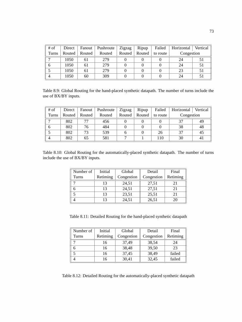
73
# of Direct Fanout Pushroute Zigzag Ripup Failed Horizontal VerticalTurns Routed Routed Routed Routed Routed to route Congestion
7 1050 61 279 0 0 0 24 516 1050 61 279 0 0 0 24 515 1050 61 279 0 0 0 23 514 1050 60 309 0 0 0 24 51
Table 8.9: Global Routing for the hand-placed synthetic datapath. The number of turns include theuse of BX/BY inputs.
# of Direct Fanout Pushroute Zigzag Ripup Failed Horizontal VerticalTurns Routed Routed Routed Routed Routed to route Congestion
7 802 77 456 0 0 0 37 496 802 76 484 0 0 0 38 485 802 73 539 6 0 26 37 454 802 65 581 7 1 110 30 41
Table 8.10: Global Routing for the automatically-placed synthetic datapath. The number of turnsinclude the use of BX/BY inputs.
Number of Initial Global Detail FinalTurns Retiming Congestion Congestion Retiming
7 13 24,51 27,51 216 13 24,51 27,51 215 13 23,51 25,51 214 13 24,51 26,51 20
Table 8.11: Detailed Routing for the hand-placed synthetic datapath
Number of Initial Global Detail FinalTurns Retiming Congestion Congestion Retiming
7 16 37,49 38,54 246 16 38,48 39,50 235 16 37,45 38,49 failed4 16 30,41 32,45 failed
Table 8.12: Detailed Routing for the automatically-placed synthetic datapath
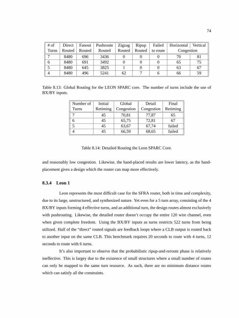
74
# of Direct Fanout Pushroute Zigzag Ripup Failed Horizontal VerticalTurns Routed Routed Routed Routed Routed to route Congestion
7 8480 696 3436 0 0 0 70 816 8480 691 3492 0 0 0 65 755 8480 645 3825 1 0 0 63 674 8480 496 5241 62 7 6 66 59
Table 8.13: Global Routing for the LEON SPARC core. The number of turns include the use ofBX/BY inputs.
Number of Initial Global Detail FinalTurns Retiming Congestion Congestion Retiming
7 45 70,81 77,87 656 45 65,75 72,81 675 45 63,67 67,74 failed4 45 66,59 68,65 failed
Table 8.14: Detailed Routing the Leon SPARC Core.
and reasonably low congestion. Likewise, the hand-placed results are lower latency, as the hand-
placement gives a design which the router can map more effectively.
8.3.4 Leon 1
Leon represents the most difficult case for the SFRA router, both in time and complexity,
due to its large, unstructured, and synthesized nature. Yet even for a 5 turn array, consisting of the 4
BX/BY inputs forming 4 effective turns, and an additional turn, the design routes almost exclusively
with pushrouting. Likewise, the detailed router doesn’t occupy the entire 120 wire channel, even
when given complete freedom. Using the BX/BY inputs as turns restricts 522 turns from being
utilized. Half of the “direct” routed signals are feedback loops where a CLB output is routed back
to another input on the same CLB. This benchmark requires 20 seconds to route with 4 turns, 12
seconds to route with 6 turns.
It’s also important to observe that the probabilistic ripup-and-reroute phase is relatively
ineffective. This is largey due to the existence of small structures where a small number of routes
can only be mapped to the same turn resource. As such, there are no minimum distance routes
which can satisfy all the constraints.
75
8.4 Summary
This chapter describes the new routing algorithms needed for a corner-turn architecture.
Routing for the corner-turn architecture is very fast, utilizing polynomial time heuristics for global
routing and channel-packing for detailed routing. The multiple phases of global routing are less
thanO(n2) in the worst case, with most steps requiringO(n lg n) time. These steps also require
only linear memory usage. Even the largest benchmark requires less than 20 seconds to route in the
worst case, 12 seconds when targeting the final SFRA’s parameters.
The final routing quality, when targeting the SFRA architecture, The results when target-
ing the basic SFRA architecture are good, enabling all benchmarks to be routed with the SFRA’s
final parameters of 6 turns and 120 wire channels.

76
Chapter 9
Other Implications of the Corner-Turn
Interconnect
In addition to fast routing algorithms and pipelined interconnect, the corner-turn intercon-
nect offers several other advantages, including defect tolerance, fixed routing overhead, and asym-
metric routing channels. Additionally, it is reasonably straightforward to embed memory blocks
and to provide hardware-assisted detailed routing.
9.1 Defect Tolerance
Any defective resource can be trivially mapped around, if an identical but unused resource
is available to replace it and if the defect does not otherwise cause operational side-effects.
Since the C-boxes in a corner-turn FPGA remain active as full crossbars, if there is a
spare bundle of connections, any breaks in the interconnect can be routed around by transposing
connections. If the bundle is located on the innermost routing track, most breaks and stuck-off de-
fects in the C-boxes themselves can also be routed around, by ensuring that any affected connection
is rerouted onto the innermost bundle. Figure 9.1 shows how a connection, which would utilize a
broken interconnect point, can be routed around. This same technique can route around stuck-on
and stuck-off connections from the local hierarchy to the general interconnect as well as problems
with the general interconnect’s rebuffering.
Of greater interest is whether stuck-on faults in the C-boxes can be avoided. The ability
to transpose connections depends on the nature of the fault. If the fault would cause no other side
effect if maintained, such as a stuck-on buffer driving an otherwise unused line, than the affected
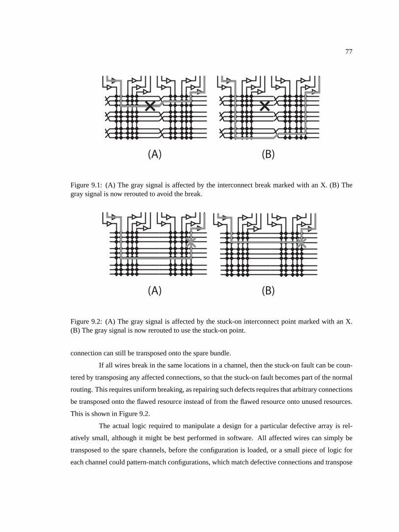
77
(A) (B)
Figure 9.1: (A) The gray signal is affected by the interconnect break marked with an X. (B) Thegray signal is now rerouted to avoid the break.
(A) (B)
Figure 9.2: (A) The gray signal is affected by the stuck-on interconnect point marked with an X.(B) The gray signal is now rerouted to use the stuck-on point.
connection can still be transposed onto the spare bundle.
If all wires break in the same locations in a channel, then the stuck-on fault can be coun-
tered by transposing any affected connections, so that the stuck-on fault becomes part of the normal
routing. This requires uniform breaking, as repairing such defects requires that arbitrary connections
be transposed onto the flawed resource instead of from the flawed resource onto unused resources.
This is shown in Figure 9.2.
The actual logic required to manipulate a design for a particular defective array is rel-
atively small, although it might be best performed in software. All affected wires can simply be
transposed to the spare channels, before the configuration is loaded, or a small piece of logic for
each channel could pattern-match configurations, which match defective connections and transpose

78
them onto spare channels.
As interconnect represents at least 3/4 of the resources in the SFRA architecture, and this
scheme allows one defect to occur in each independent routing channel, the actual number of defects
tolerated is substantial when considered over the entire die.
9.2 Memory Blocks
Semantically,C-slowed RAM behaves somewhat differently from conventional RAMs,
as the high address bits are derived from aC index counter to isolate each thread’s memory. More
details of these semantics are included in Chapter 10.
When embedding memory blocks in a fixed-frequency FPGA, there are two options: ex-
pose all the address bits and require that the counter be externally generated, or hide the upper
address bits and use an internal counter.
Exposing all the address bits gains maximum flexibility, but requires more interconnect
resources, as now more address bits need to be routed to each memory block. One useful possibility
is to provide a dedicated counter for each column of memory blocks, which drives onto vertical
wires. Since most memories will operate on the sameC-factor, all memory block can safely share
the same counter, even though the counter is out of phase with respect to the different blocks.
This also reduces the general interconnect load, as the high bits are now primarily driven
by the vertical column, with no switches being used to route the connections. Especially in a corner-
turn network, where switches are a limited resource, sharing the switch capacity among all memory
blocks offers substantial savings.
Even without a dedicated counter in each column, the interconnect costs will, in practice,
be relatively low. Due to the high fanout of such counters, the router will preferentially route the
tread count using a single switch per bit, onto the vertical channel associated with each stripe of
memory.
Thus although exposing all address wires for the memories may result in additional inter-
connect cost, the total cost will be reasonable as the router will tend to insure that each bit in the
counter only uses one switch per column of memories, due to the high-fanout nature of these counter
bits. This suggests that large memory blocks should expose all address bits rather than hiding the
upper bits through the use of internal counters.
79
9.3 Hardware Assisted Routing
Although there is less clear benefit for hardware-assisted routing, given that the corner-
turn structure has fast global and detailed routing algorithms, a version with depopulated C-boxes
might benefit from hardware assisted routing.
The scheme, proposed in Huang et al [33], relies on the observation of limited crossover
points and parallel searching of a large search space. Since global routing has very limited freedom,
and it is unclear how to transpose (rather than rip-up) connections in hardware, this scheme is not
easily adapted to global routing.
Detailed routing, however, is probably adaptable to the Huang scheme, albeit with a mod-
ification. The basic concept of the scheme is to search all possible routes in parallel with a signal
broadcast from the source and to randomly remove an existing set of signals when conflicts arise.
If each rebuffering connection in the interconnect has an additional bit to record when
a connection is used, as well as an additional bit for each connection between an output and the
general interconnect, the Huang scheme can be employed to perform detailed routing.
In this scheme, an output which wishes to be routed broadcasts a search signal, which
is then propagated on all connections where no signal is currently active. If this signal reaches the
destination, this is used to guide allocation of the signal. Otherwise, a random channel is victimized.
This may be useful if depopulated C-boxes are utilized, but as the current intercon-
nect uses fully populated C-boxes, enabling fastO(n lg n) software routing, it is unclear whether
hardware-assisted routing is desirable when using a corner-turn interconnect.
It may also be possible to perform hardware-assisted global routing during the pushroute
phase, although it will clearly be less efficient than pushrouting. For hardware-assisted routing, the
two possible global routes are examined. If both are free, one is randomly allocated. If neither
global route is free, a random route is selected for victimization.
This random victimization will act as a random walk along the possible pushroute search
path. Thus if there is only a minor amount of routing pressure, it should be possible to find a
solution. If routing pressure is more significant, this mechanism will generally fail as it is far less
effective than a comprehensive search.

80
9.4 Heterogeneous channels
It is commonly observed that most FPGA designs follow Rent’s Rule[39, 21]. In this for-
mulation, the bisection bandwidth of the design is relatively reduced the farther up in the hierarchy.
Yet as designs get larger, the overall interconnect requirement increases.
When such designs are placed with conventional placement tools, the center of the array
may be more congested than the periphery. This becomes more prevelant when an FPGA, as part
of a larger system-on-a-chip, uses a non-rectangular layout. Thus it has been suggested that FPGAs
might have heterogeneous channels [29], where the X and Y channels are of significantly different
capacity. Additionally, it has been considered (although Betz and Rose argue against this in [10])
that an FPGA could contain more routing resources near the center.
A corner-turn interconnect can easily support such channels. As the C-boxes remain as
full crossbars, reducing the capacity of a given channel has no effect on the other channels in the
array or the routing problem. Thus the outside channels can be reduced in capacity without a
significant effect on the rest of the design.
Additionally, the layout used by the SFRA is highly adaptable to a variable channel-width,
as the channel itself consists of a replicated series of tiles. By removing the tiles in the middle which
represent a bundle of wires, the channel can be reduced in capacity without permuting any other
portion of the layout. Thus unlike previous architectures, a corner-turn network can easily support
this style without serious impacting either the toolflows or the layout complexity.
9.5 Summary
Beyond fast-routing and pipelinable interconnect, a corner-turn architecture has some
other implications. This style of interconnect can tolerate numerous defects in the channel by sim-
ply transposing around faults. Memory blocks can easily be integrated into this structure, without a
significant concern for the extra address bits required for aC-slowed memory block. There is some
potential for hardware-assisted routing if this feature is desirable. Finally, this style of interconnect
can easily support heterogeneous channels.

81
Part II
Retiming
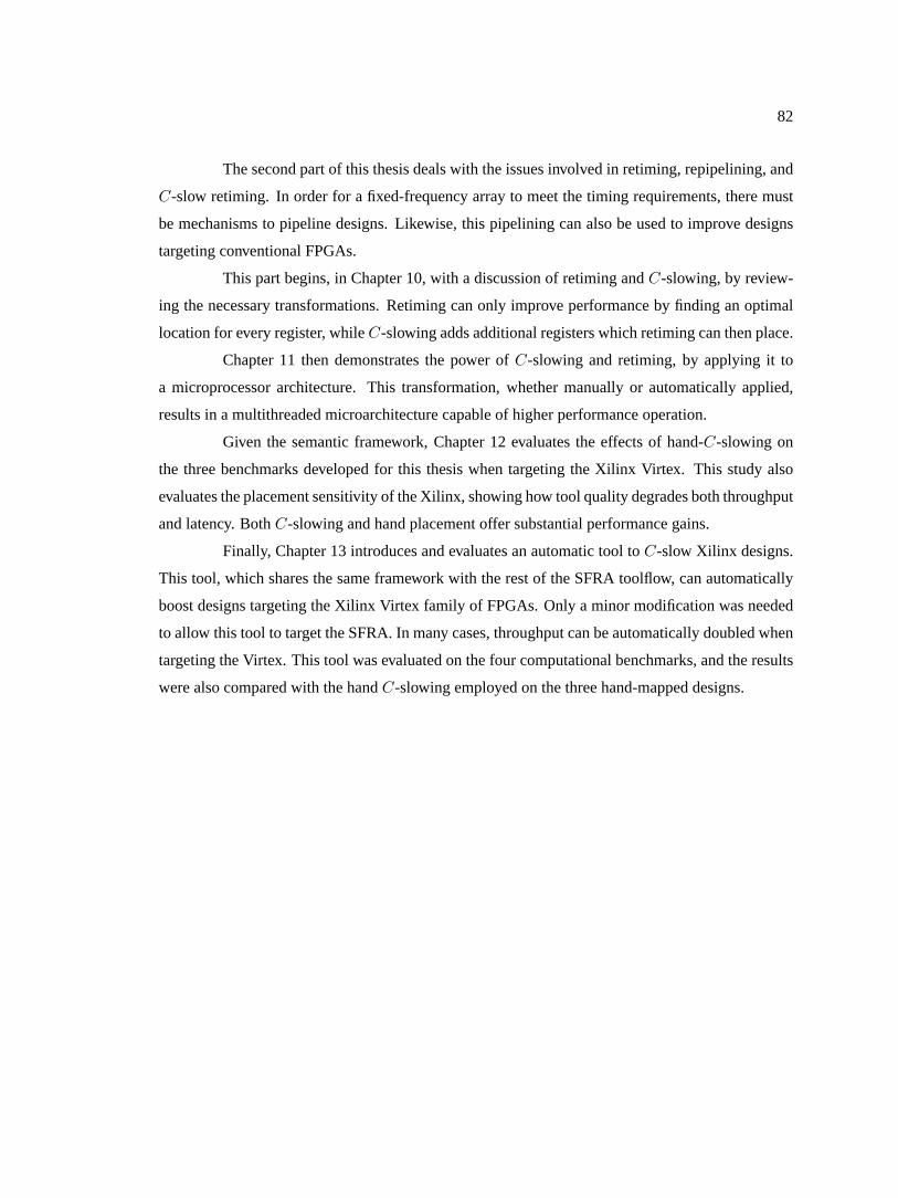
82
The second part of this thesis deals with the issues involved in retiming, repipelining, and
C-slow retiming. In order for a fixed-frequency array to meet the timing requirements, there must
be mechanisms to pipeline designs. Likewise, this pipelining can also be used to improve designs
targeting conventional FPGAs.
This part begins, in Chapter 10, with a discussion of retiming andC-slowing, by review-
ing the necessary transformations. Retiming can only improve performance by finding an optimal
location for every register, whileC-slowing adds additional registers which retiming can then place.
Chapter 11 then demonstrates the power ofC-slowing and retiming, by applying it to
a microprocessor architecture. This transformation, whether manually or automatically applied,
results in a multithreaded microarchitecture capable of higher performance operation.
Given the semantic framework, Chapter 12 evaluates the effects of hand-C-slowing on
the three benchmarks developed for this thesis when targeting the Xilinx Virtex. This study also
evaluates the placement sensitivity of the Xilinx, showing how tool quality degrades both throughput
and latency. BothC-slowing and hand placement offer substantial performance gains.
Finally, Chapter 13 introduces and evaluates an automatic tool toC-slow Xilinx designs.
This tool, which shares the same framework with the rest of the SFRA toolflow, can automatically
boost designs targeting the Xilinx Virtex family of FPGAs. Only a minor modification was needed
to allow this tool to target the SFRA. In many cases, throughput can be automatically doubled when
targeting the Virtex. This tool was evaluated on the four computational benchmarks, and the results
were also compared with the handC-slowing employed on the three hand-mapped designs.

83
Chapter 10
Retiming, C-slow Retiming, and
Repipelining
Retiming, a process originally developed by Leiserson et al [41], is a process which can
automatically increase the clock rate of a circuit by finding an optimal placement for all registers
to minimize the critical path. Two variants, repipelining andC-slow retiming, offer the ability to
reduce the critical path still further by adding additional registers before retiming proceeds.
Although an important optimization for conventional FPGAs, retiming is a critical frame-
work for developing fixed-frequency architectures. In order to meet the array’s fixed-frequency, a
design must ensure that every path is properly registered. Repipelining orC-slow retiming enables
a design to be transformed to meet these constraints. Without automated repipelining orC-slow
retiming, the designer must manually ensure that these constraints are met by the design.
Thus, for a complicated design targeting a fixed-frequency architecture, automatedC-
slowing or repipelining is essential. Without this transformation, designers are restricted to using
tools or creating designs which meet the architectural constraints without modification. Such a
restriction is obviously unacceptable.
AlthoughC-slow retiming can be applied to both conventional FPGAs and fixed-frequency
architectures, the process is considerably faster (O(n2) rather thanO(n2 lg n)) and requires less
memory (O(n) rather thanO(n2)) when targeting a fixed-frequency architecture like the SFRA
instead of a conventional architecture like the Virtex.
84
Condition Constraint
normal edge fromu → v r(u)− r(v) ≤ w(e)edge fromu → v r(u)− r(v) ≤ w(e)− 1must be registerededge fromu → v r(u)− r(v) ≤ 0 andcan never be registered r(v)− r(u) ≤ 0Critical Paths r(u)− r(v) ≤ W (u, v)− 1must be registered for all u, v such thatD(u, v) > P
Table 10.1: The constraint system used by the retiming process.r(u) is the lag computed for eachnode,w(e) is the initial number of registers on an edge,W (u, v) is the minimum number of registersbetweenu andv, andD(u, v) is the critical path betweenu andv
10.1 Retiming
Leiserson’s retiming treats a synchronous circuit as a directed graph, with delays on the
nodes representing combination delays and weights on the edges representing registers in the design.
An additional node represents the external world, with appropriate edges added to account for all
the I/Os. Two matrices are calculated,W andD, that represent the number of registers and critical
path between every pair of nodes in the graph. Each node also has a lag valuer that is calculated by
the algorithm and used to change the number of registers which will be placed on any given edge.
Conventional retiming does not change the design semantics: all input and output timings remain
unchanged, while minor design constraints are imposed on the use of FPGA features. More details
and formal proofs of correctness can be found in Leiserson’s original paper [41].
A graphical example of the results is shown in Figure 10.1. The initial graph has a critical
path of 5, which is clearly non-optimal. After retiming, the graph now has a critical path of 4. Yet
the I/O semantics have not changed, as any input will still require 3 cycles to affect the output.
In order to determine whether a critical pathP can be achieved, the retiming algorithm
creates a series of constraints to calculate the lag on each node. All these constraints are of the form
x − y ≤ k that can be solved inO(n2) time by using the Bellman/Ford shortest path algorithm.
The primary constraints ensure correctness: no edge will have a negative number of registers, while
every cycle will always contain the original number of registers. All IO passes through an interme-
diate node insuring that input and output timings do not change. These constraints can be modified
to ensure that a particular line will contain no registers or a mandatory minimum number of registers
to meet architectural constraints without changing the complexity of the equations.
85
(A) (B)
IN OUT
1 1
1 1 22 IN OUT
1 1
1 1 22
Figure 10.1: (A): A small graph before retiming. The nodes represent logic delays, with the inputsand outputs passing through mandatory, fixed registers. The critical path is 5. The input and outputregisters can not be moved. (B): The same graph after retiming. The critical path is reduced from 5to 4. Yet the I/O semantics have not changed, as it still requires three cycles for a datum to proceedfrom input to output.
A second set of constraints attempts to ensure that every path longer than the critical
path will contain at least one register, by creating an additional constraint for every path longer
than the critical path. Calculating theses constraints requires solving the “all-pairs shortest-path”
problem to determine the critical path from every node to every other node. The actual constraints
are summarized in Table 10.1.
This process is iterated to find the minimum critical path that meets all the constraints.
The lag calculated by these constraints can then be used to change the design to meet this critical
path. For each edge, a new register weightw′ is calculated, withw′(e) = w(e)− r(u) + r(v).
In practice, the Bellman/Ford process can be radically shortcutted. If the solution exists,
the constraint solver tends to converge very quickly. Thus, if an iteration does not change any of the
edge weights, a solution has been discovered and the process halts. Thus without a practical loss in
quality, The process can arbitrarily halt after a few dozen or hundred iterations.
A second optimization is to utilize the last computed set as a starting point.1 In conven-
tional retiming, the Bellman/Ford process is invoked multiple times to find the lowest satisfiable
critical path, while fixed-frequency repipelining orC-slow retiming uses the Bellman/Ford algo-
rithm to discover the minimum amount of additional registers needed to satisfy the constraint. In
both cases keeping the last failed or successful solution in the data structure provides a starting point
which can significantly speed the process if a solution exists.
The biggest problem with the Leiserson approach is the computation of theW andD
1This optimization was discovered by accident, when the previous solution was not erased from the data structure.
86
matrices for general retiming.2 The simplistic approach, using Dijkstra’s algorithm, requiresO(n3)
time andO(n2) space. Solving the all-pairs shortest-path problem, which needs a matrix represen-
tation, still requiresO(n2lg(n)) time andO(n2) space.
Retiming in this form imposes only minimal design limitations: there can be no asyn-
chronous resets or similar elements, as it only applies to synchronous circuits. A synchronous
global reset imposes too many constraints to allow effective retiming. Local synchronous resets and
enables just produce small, self loops that have no effect on the correct operation of the algorithm.
Most other design features can be accommodated simply by adding appropriate con-
straints. As an example, all tristated lines can not have registers applied to them, while mandatory
elements, such as those seen in synchronous memories or mandated I/O registers, can be easily
accommodated by mandating registers on the appropriate nets.
Memories themselves can be retimed like any other element in the design, with dual
ported memories treated as a single node for retiming purposes. Memories that are synthesized
with a negative clock edge (to create the design illusion of asynchronous memories) can either be
unchanged or switched to operate on the positive edge with constraints to mandate the placement of
registers.3
Initial register conditions can also be calculated if desired, but this process is NP hard in
the general case. Cong and Wu [20] have an algorithm that computes initial states by restricting the
design to forward retiming only, so it propagates the information and registers forward throughout
the computation. This is because solving initial states for all registers moved forward is straightfor-
ward, but backward movement is NP hard,4 as it reduces to satisfiability.
Likewise, the computing of initial conditions proves very costly in practice. In the ASIC
model, all flip-flops start in an undefined state, and the designer must create a small state machine
in order to reset the design. FPGAs, however, have all flip-flops start in a known, user defined state.
When a dedicated global reset is applied, all theses flip-flops are reset into this known state. This has
serious implications in retiming. If the decision is made to utilize the ASIC model, then retiming is
free to safely ignore initial conditions because explicit reset logic in state machines will still operate
correctly as this is reflected in the I/O semantics. However without the ability to violate the initial
conditions with an ASIC-style model, retiming quality often suffers, as additional logic is required
or limits are placed on where flip-flops may be moved in a design.
2Fortunately, as discussed later, this step is not required for fixed-frequency retiming.3For some cases, this may produce a set of unsolvable constraints, thus requiring that the memory remain a negative
edge device.4And may not posses a valid solution for nonsensical cases.
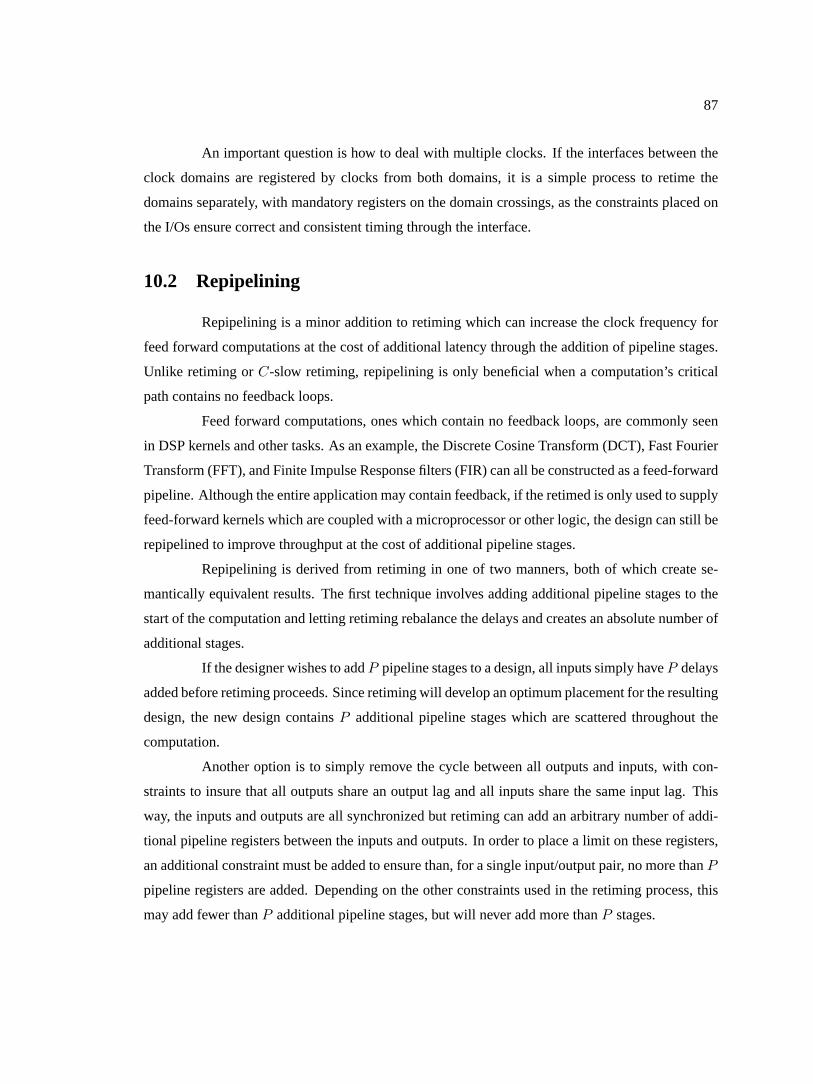
87
An important question is how to deal with multiple clocks. If the interfaces between the
clock domains are registered by clocks from both domains, it is a simple process to retime the
domains separately, with mandatory registers on the domain crossings, as the constraints placed on
the I/Os ensure correct and consistent timing through the interface.
10.2 Repipelining
Repipelining is a minor addition to retiming which can increase the clock frequency for
feed forward computations at the cost of additional latency through the addition of pipeline stages.
Unlike retiming orC-slow retiming, repipelining is only beneficial when a computation’s critical
path contains no feedback loops.
Feed forward computations, ones which contain no feedback loops, are commonly seen
in DSP kernels and other tasks. As an example, the Discrete Cosine Transform (DCT), Fast Fourier
Transform (FFT), and Finite Impulse Response filters (FIR) can all be constructed as a feed-forward
pipeline. Although the entire application may contain feedback, if the retimed is only used to supply
feed-forward kernels which are coupled with a microprocessor or other logic, the design can still be
repipelined to improve throughput at the cost of additional pipeline stages.
Repipelining is derived from retiming in one of two manners, both of which create se-
mantically equivalent results. The first technique involves adding additional pipeline stages to the
start of the computation and letting retiming rebalance the delays and creates an absolute number of
additional stages.
If the designer wishes to addP pipeline stages to a design, all inputs simply haveP delays
added before retiming proceeds. Since retiming will develop an optimum placement for the resulting
design, the new design containsP additional pipeline stages which are scattered throughout the
computation.
Another option is to simply remove the cycle between all outputs and inputs, with con-
straints to insure that all outputs share an output lag and all inputs share the same input lag. This
way, the inputs and outputs are all synchronized but retiming can add an arbitrary number of addi-
tional pipeline registers between the inputs and outputs. In order to place a limit on these registers,
an additional constraint must be added to ensure than, for a single input/output pair, no more thanP
pipeline registers are added. Depending on the other constraints used in the retiming process, this
may add fewer thanP additional pipeline stages, but will never add more thanP stages.
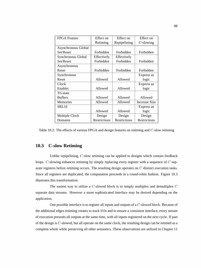
88
FPGA Feature Effect on Effect on Effect onRetiming Repipelining C-slowing
Asynchronous GlobalSet/Reset Forbidden Forbidden ForbiddenSynchronous Global Effectively EffectivelySet/Reset Forbidden Forbidden ForbiddenAsynchronousReset Forbidden Forbidden ForbiddenSynchronous Express asReset Allowed Allowed logicClock Express asEnables Allowed Allowed logicTri-stateBuffers Allowed Allowed AllowedMemories Allowed Allowed Increase SizeSRL16 Express as
Allowed Allowed logicMultiple Clock Design Design DesignDomains Restrictions Restrictions Restrictions
Table 10.2: The effects of various FPGA and design features on retiming andC-slow retiming
10.3 C-slow Retiming
Unlike repipelining,C-slow retiming can be applied to designs which contain feedback
loops. C-slowing enhances retiming by simply replacing every register with a sequence ofC sep-
arate registers before retiming occurs. The resulting design operates onC distinct execution tasks.
Since all registers are duplicated, the computation proceeds in a round-robin fashion. Figure 10.3
illustrates this transformation.
The easiest way to utilize aC-slowed block is to simply multiplex and demultiplexC
separate data streams. However a more sophisticated interface may be desired depending on the
application.
One possible interface is to register all inputs and outputs of aC-slowed block. Because of
the additional edges retiming creates to track I/Os and to ensure a consistent interface, every stream
of execution presents all outputs at the same time, with all inputs registered on the next cycle. If part
of the design isC-slowed, but all operate on the same clock, the resulting design can be retimed as a
complete whole while preserving all other semantics. These observations are utilized in Chapter 11
89
(A) (B)
IN OUT
1 1
1 1 22 IN OUT
1 1
1 1 22
Figure 10.2: (A): The example from Figure 10.1 which is converted to2-slow operation. The criticalpath remains unchanged, but now the design will operate on two independant streams in a round-robin fashion. (B): The design is now retimed. By taking advantage of the extra flip-flops, thecritical path has been reduced from 5 to 2.
when discussing the effects ofC-slowing on a microprocessor core.
However,C-slowing imposes some more significant FPGA design constraints, as sum-
marized in Table 10.2. Register clock enables and resets must be expressed as logic features, since
each independent thread must see a different view of the reset or enable. Thus, they can remain
features in the design but can not be implemented by current FPGAs using the native enables and
resets. Other specialized features, such as Xilinx SRL16s,5 can not be utilized in aC-slow design
for the same reasons.
One important challenge is how to properlyC-slow memory blocks. In most cases, one
desires the complete illusion that each stream of execution is completely independent and un-
changed. To create this illusion, the memory capacity must be increased by a factor ofC, with
additional address lines driven by a counter. This ensures that each stream of execution enjoys a
completely separate memory space.
For dual-ported memories, this potentially enables a greater freedom in retiming: the two
ports can have different lags, as long as the difference in lag isC − 1 or less. After retiming, the
difference in lag is added to the appropriate port’s thread counter. This modification ensures that
each stream of execution will read and write to both ports in order, while enabling slightly more
freedom for retiming to proceed. However, this optimization is not used in the tools targeting either
the SFRA or the Xilinx.
C-slowing normally guarantees that all streams view independent memories. However a
designer may desire shared memory common to all streams. Such memories could be embedded in
a design but the designer would need to consider how multiple streams would affect the semantics
5A mode where the LUT can act as a 16 bit shift register
90
and would need to notify any automatic tool to treat the memory in a special manner. Otherwise,
there are no other semantic effects imposed byC-slow retiming.
10.4 Retiming for Conventional FPGAs
Most FPGA architectures are especially amenable to repipelining orC-slow retiming,
as the FPGAs are generally register-rich when compared with most designs. Thus increasing the
number of registers will not necessarily create a larger design, if the registers are well-allocated.
An additional benefit for many architectures is the ability to separately use the logic cells
and registers under a wide variety of conditions. This enables registers to be used that would other-
wise go completely unused in a design without impacting the logic utilization.
When retiming for FPGAs, the location of retiming in the toolflow is an important con-
sideration: it can occur before, during, or after the placement process. There are advantages and
disadvantages for all three approaches.
Before-placement is often the simplest but may encounter some limitations. Such retiming
simply estimates interconnect delay, performs retiming, and then lets the packing and placement
tools proceed.
If the placement tool only places complete cells, rather than district elements, the retiming
tool can’t effectively scavenge unused flip-flops without distorting the placement process. This is
because packing unrelated logic will cause the placement tool to perform poorly, as the compromise
position for the unrelated logic is often significantly unoptimal.
Another disadvantage with pre-placement retiming is the significant factor that intercon-
nect delays play in FPGA timing. Thus, any retiming tools gains substantial benefits from a detailed
understanding of the interconnect delays in a design, information which can only be crudely esti-
mated before placement occurs.
Yet preplacement retiming offers the potential ability to combine logic by moving regis-
ters. As an example, assume that a design contains a 2 input logic function, a register, and then
another two input logic function. If the retiming tool moves the register in either direction, the re-
sulting design can be packed into a single 4-LUT instead of two independent 4-LUTs, saving both
area and reducing the critical path.
Post-placement retiming is also convenient, as the delays are now all completely known
and flip flops can be safely scavenged without affecting the placement process. The main difficulties
occur when attempting a large degree ofC-slowing, because allocating large numbers of flip-flops
91
can prove problematic unless placements are modified.
A combined placement and retiming tool is the ideal solution, except that it may require
a partial or complete restructuring of the placement process. Such a tool, such as Singh’s [63], can
even perform effective retiming when a large number of registers need to be allocated, as it can then
permute the design’s placement during the allocation process.
The need for mixed placement and retiming depends heavily on the target architecture.
Singh’s target, the academic Toronto model [11], has the flip-flop only driveable from the LUT
output. Thus to scavenge an unused flip-flop, the LUT can’t be used either. Thus post-placement
retiming would often have to use a flip-flop a greater distance away, even when a closer, unused flip-
flop was available, simply because the associated LUT was used. Thus this tool benefited greatly
from combined placement and retiming, even for retiming withoutC-slowing.
This contrasts sharply with the commercial FPGAs. The Xilinx Virtex’s [82] Flip Flop
can be used independently except when the carry chain is driven or initiated, the F5 or F6 muxes
utilized, or the BX/BY inputs are used for routing. Similarly, the Altera Stratix [4] can use a flip-
flop as a LUT input instead of an output or use the flip-flop independently when the LUT is only
used as a 3-LUT instead of a 4-LUT.
When the Flip-Flop can be used independently of the associated LUT, the advantages
of mixed placement/retiming become less significant, as the tool can more easily obtain new flip-
flops from unused logic. Similarly, when long-delay chains are required, an intelligent heuristic
could create a chain of long-delay paths which would scavenge most of the flip-flops from the low-
congestion areas outside the critical regions. Thus, although combined placement/retiming offers
some advantages, these advantages are diminished on modern FPGAs.
It is for this reason that the tool created to retime Virtex designs (described in Chapter 13)
uses post-placement retiming, as the Virtex is very ameniable to post-placement flip-flop scaveng-
ing.
10.5 Retiming for Fixed Frequency FPGAs
Unlike conventional FPGAs, retiming for fixed frequency FPGAs does not require the
creation of a global critical-path constraint, as simply insuring all local requirements will guarentee
that the final design meets the architecture’s critical path. Instead, retiming attempts to solve these
local constraints: ensuring that every path through the interconnect meets the delay model inherent
in the FPGA. Once these local constraints are met, the final design will operate at the array’s clock
92
frequency.
Because there are no longer global constraints, theW andD matrixes are not created.
This results in substantial savings as theO(n3) Dijkstra’s step or theO(n2 lg n) optimal solution
for the all-pairs shortest-path problem dominates execution time, while theW and D matrixes
requireO(n2) memory.
Since a fixed-frequency FPGA doesn’t require the global constraints, having to just solve
a set of local constraints requires linear, not quadratic memory andO(n2) rather thanO(n2lg(n))
execution time. This speeds up the retiming process considerably.
Additionally, only a single invocation of the constraint solver is necessary to determine
whether the current level of pipelining can meet the constraints imposed by the target architecture.
Unfortunately, most designs do not possess sufficient pipelining to meet these constraints, instead
requiring a significant level of repipelining orC-slow retiming to meet the constraints. This level
can be discovered in two ways.
The first solution is simply to allow the user to specify a desired level of repipelining or
C-slowing. The retiming system then adds the specified number of delays and attempts to solve the
system. If a solution is discovered, it is used. Otherwise the user is notified that the design can’t be
repipelined or retimed to meet the desired constraints for the given level ofC-slowing.
The second requires searching to find the minimal level of repipelining orC-slowing
necessary to meet the constraints. Although this requires multiple iterations of the constraint solver,
fixed-frequency retiming only requires local constraints. Without the task of developing the global
constraints, this process proceeds quickly. Due to this searching and the lack of global constraints
in fixed frequency retiming, it is probably best to use a series of additional registers on the input
to perform repipelining, as this creates a design with the minimum number of additional pipeline
stages. The tool developed for the SFRA uses the latter approach: finding the minimumC-slow
retiming required to meet the fixed-frequency constraints.
Unlike conventional FPGAs, fixed-frequency FPGAs require retiming considerably later
in the toolflow. Until routing delays are known, it is impossible to create a valid retiming. Since
invariably the constraints required depend on placement, the final retiming process must occur after-
wards. Some arrays, such as the HSRA [74] have deterministic routing structures, enabling retiming
to be performed either before or after routing. Other interconnect structures, such as the SFRA, lack
deterministic routing and require retiming to be performed after routing. Thus the SFRA retiming
tool, although it performs an initial retiming before routing, can only create a final retiming after
routing completes.
93
Finally, as fixed-frequency arrays may use considerably more pipelining than conven-
tional arrays, retiming registers are a significant architectural feature. These programmable delay
chains (discussed in more detail in Chapter 6), either on inputs or outputs, allow the array to imple-
ment longer delay chains. A common occurrence after aggressiveC-slow retiming is a design with
several signals requiring considerable delay. Therefore, dedicated resources to implement these
features are effectively required to create a viable fixed-frequency FPGA.
10.6 Previous Retiming Tools
There have been no published commercial or academicC-slow retiming or repipelining
tool-flows apart from flow developed by DeHon et al for the HSRA [74]. The retiming process was
accomplished by modifying the design and callingsis , havingsis retime the resulting design.6
Since the HSRA contained a deterministic network, only placement information was required for
retiming to proceed.
Conventional retiming is far more common. There have been two previously significant
academic retiming tools targeted towards FPGAs. The first, by Cong and Wu [20] combined retim-
ing with technology mapping. This approach enables retiming to occur before placement without
adding undue constraints on the placer, since the retimed registers are packed only with their asso-
ciated logic. The disadvantage is lack of precision, as delays can only be crudely estimated before
placement. It is unsuitable for significantC-slowing asC-slowing creates significantly more regis-
ters which can pose problems with logic packing and placement.
The second, by Singh and Brown [63], combined retiming with placement. This operated
by modifying the placement algorithm to be aware that retiming was occurring and then modifying
the retiming portion to enable permutation of the placement as retiming proceeds. They demon-
strated how combining placement and retiming performs significantly better than retiming either
before or after placement.
The simplified FPGA model used has a logic block where the flip-flop cannot be used
independently of the LUT, constraining the ability of post-placement retiming to allocate new reg-
isters. Thus, the need to permute the placement to allocate registers is significantly exacerbated in
their target architecture.
Some commercial HDL synthesis tools, notably Synopsys FPGA Compiler [72] and Syn-
6Chameleon Systems was developing a retiming andC-slowing system for their architecture but public informationis not available and the company is currently defunct.

94
plify [71] also support retiming. Because this retiming occurs fairly early in the mapping and
optimization processes, it suffers from a lack of precision about placement and routing delays. The
Amplify tool [70] can produce a higher quality retiming because it contains placement informa-
tion. Likewise, since these tools attempt to maintain the FPGA model of initial conditions, both on
startup and in the face of a global-reset signal, this adds considerable logic to the design.
10.7 Summary
This section reviewed the semantics of the retiming process, repipelining, andC-slow
retiming, and how these processes interact with both conventional and fixed-frequency FPGAs. On
a conventional FPGA, retiming andC-slow retiming offer improved performance with only mild
semantic restrictions, albeit requiringO(n2) memory andO(n2lg(n)) time. On a fixed-frequency
FPGA,C-slow retiming is an essential transformation, requiringO(n) memory andO(n2) time.
95
Chapter 11
Applying C-Slow Retiming to
Microprocessor Architectures
C-slow retiming applies to all designs which are capable of using the task level parallelism
provided, regardless of the design’s complexity. Since it represents an automatic transformation, it
can be applied to a diverse number of applications and designs.
One of the more fascinating observations is that the core of a microprocessor can be
C-slow retimed. The resulting core has multithreaded semantics identical to an “Interleaved Multi-
threaded” [40] architecture operating at a higher clock rate. Each individual thread runs slower, but
the aggregate throughput is increased as now multiple tasks can be completed in parallel, sharing
the hardware.
Although the created architecture is semantically an interleaved-multithreaded architec-
ture, this is a unique and novel approach for two reasons: it represents an automatically applied
transformation and offers higher throughput, not simply memory-utilization advantages.
11.1 Introduction
There have been numerous multithreaded architectures, but they all share a common
theme: increase system throughput by enabling multiple streams of execution, or threads, to op-
erate simultaneously. These architectures generally fall into four classes: context-switching always
without bypassing (HEP [66] and Tera [6]), context-switching on event (Intel IXP [35]), interleaved-
multithreaded, and Symmetric Multithreaded (SMT) [75].
The ideal goal of all these architectures is to increase system throughput by operating

96
on multiple streams of execution. Ideally, every stream is unaffected by other running streams,
but some interference effects may occur. Appendix B includes a more detailed survey of previous
multithreaded architectures and where interference and synergistic effects happen.
The general concept ofC-slow retiming [41] (discussed in more detail in Chapter 10) can
be applied to highly complex designs, including microprocessors. Unlike a filterbank or encryp-
tion algorithm, it is not simply a matter of inserting registers and balancing delays. Nevertheless,
the changes necessary are comparatively small and the benefits substantial: producing a simple,
statically scheduled, higher clock rate, multithreaded architecture which is semantically equivalent
to an interleaved-multithreaded architecture: alternating between a fixed number of threads in a
round-robin fashion, to create the illusion of a multiprocessor system.
Unlike the interleaved-multithreaded architecture, theC-slowed core offers two advan-
tages: it can be largely constructed through an automatic transformation, and the resulting design
operates at a higher clock rate, improving throughput as well as memory behavior.
C-slowing requires three minor architectural changes: enlarging and modifying the regis-
ter file and TLB, slightly modifying the interrupt semantics, and replacing the caches and memory
interface. Beyond that, it is simply a matter of replacing every pipeline register in both the control
logic and datapath withC registers, then moving the registers to balance the delays, as is traditional
in theC-slow retiming transformation and which can be performed by an automatic tool. The re-
sulting design, as expected, has full multithreaded semantics and improved throughput through a
significantly higher clock rate.
If the core itself isC-slowed, and the cache and I/O logic restructured to accommodate
the changes, the resulting design can operate at a significantly higher throughput as now there is
significantly finer pipelining. The automaticC-slow tool, discussed in Chapter 13, shows that it
is possible to effectively double the throughput on a design consisting of a conventional 5-stage
pipeline, at a reasonable cost in area, when creating a 2-thread processor.
11.2 C-slowing a Microprocessor
An alternative approach to both interleaved-multithreading (which doesn’t take advantage
of finer pipelining opportunities) and SMT designs is to start with a conventional core andC-slow
the design: inserting additional register stages and thereby increasing the clock rate through finer
pipelining. This can obviously be applied to microarchitectures where the clock period used is
significantly longer than that supported by the process and where the applications would benefit
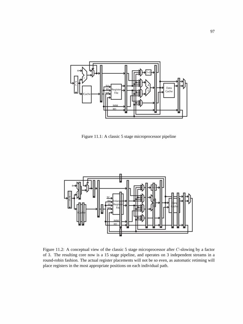
97
RegisterFile
RARB
IMMRD
ALU
?=0
DataCache
WB
+
4
PC
ICache
Figure 11.1: A classic 5 stage microprocessor pipeline
RARB
IMMRD
WB
+
4
PC
TCEnlargedRegister
File
?=0
ALU
DataCache
ICache
Figure 11.2: A conceptual view of the classic 5 stage microprocessor afterC-slowing by a factorof 3. The resulting core now is a 15 stage pipeline, and operates on 3 independent streams in around-robin fashion. The actual register placements will not be so even, as automatic retiming willplace registers in the most appropriate positions on each individual path.

98
from thread level parallelism. The resulting core will behave like an interleaved multithreaded
architecture, but will have a greater aggregate throughput achieved through the fine pipelining.
In order to avoid the complexities of deep pipelines or dynamic thread dispatch, theC-
slowed design simply switches betweenC threads on every clock cycle. The register file and trans-
lation buffers need to be increased to create an independent architectural state for each thread, while
the interrupt semantics needs minor changes to accommodate the separate threaded nature. Beyond
that, the remaining changes in the core are almost exclusively limited to those resulting from adding
and retiming the pipeline stages, which can be conducted automatically. Outside the core, including
the cache, logic must be modified to account for the new multithreaded semantics.
The biggest complications whenC-slowing a microprocessor are selecting the implemen-
tation semantics for the various memories through the design. The first type keeps the traditional
C-slow semantics of complete independence, where each thread sees a completely independent
view, usually by duplication. This applies to the register file and most of the state registers in the
system. This will occur automatically ifC-slowing is performed by a tool, as this is the normal
semantics forC-slowed memory.
The second is completely shared memory, where every thread sees the same memory,
such as the caches and main memory of the system. Most such memories exist in the non-C-slowed
portion, so are unaffected by an automatic tool.
The third is dynamically shared, where a hardware thread ID or a software thread con-
text ID is tagged to each entry, with only the valid tags being used. This is best used for branch
predictors and similar caches, and breaks the automaticC-slow semantics. Such memories need to
be constructed manually, but offer potential efficiency advantages as they don’t need to increase in
size, but can’t be constructed automatically and may be subject to interference or synergistic effects.
11.2.1 Register File
The biggest architectural changes are to the register file: it needs to be increased by a fac-
tor of C, with a hardware thread counter to select which group of registers are being accessed. Now
each thread will see an independent set of registers, with all reads and writes for the different threads
going to separate memory locations. Apart from the thread selection and natural enlargement, the
only piece remaining is to pipeline the register access. If necessary, theC independently accessed
sections can be banked, in order to allow the register file to operate at a higher clock frequency.
Naturally, this linearly increases the size of the register file, but pipelining the new larger

99
file isn’t difficult since each thread accesses a disjoint register set, allowing staggered access to the
banks if desired. This matches the automatic memory transformations whichC-slowing creates:
increasing the size and insuring that each task has an independent view of memory.
For FPGA implementations, such as the Virtex, where there already exist pipelined mem-
ory structures, no changes beyond the increase in size are required as the memories generally support
very fast, pipelined access.
11.2.2 TLB
In order to maintain the illusion that the different threads are running on completely dif-
ferent processors, it is important that each thread have an independent translation of memory. The
easiest solution is to apply the same transformations to the TLB that were applied to the register
file: increasing the size byC, with each thread accessing its own set, and pipelining access. Again,
this is the natural result of applying theC-slow semantics from an automatic tool.
The other option is to tag each TLB entry. The interference effect may be significant if the
associativity or size of the TLB is low. In such a case, and considering the generally small nature
of most TLBs, increasing the size (although perhaps by less than a factor ofC) would be advisable.
Software thread ID tags, rather than hardware ID tags, are preferable because this reduces the cost
of context switching if a shared TLB is utilized and may also provide some synergistic effects. In
either case, a shared TLB will require interlocking between TLB writes to prevent synchronization
bugs.
11.2.3 Caches and Memory
If the caches are physically addressed, it is simply a matter of pipelining access to improve
throughput without splitting the memory. Because of the interlocked execution of the threads and the
pipelined nature of the modified caches, no additional coherency mechanisms are required except
to interlock any existing test-and-set or atomic read/write instructions between the threads to insure
that each instruction has time to be completed.
Such cache modifications occur outside theC-slow semantics, suggesting that the cache
needs to be changed manually. Thus the cache and memory controller must be manually updated to
support pipelined access from the distinct threads, and exist outside of theC-slowed core itself.
Unfortunately, virtually addressed caches are significantly more complicated: they re-
quire that each tag include thread ownership (to prevent one thread from viewing another’s version
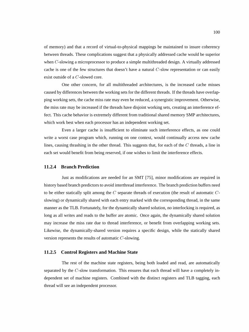
100
of memory) and that a record of virtual-to-physical mappings be maintained to insure coherency
between threads. These complications suggest that a physically addressed cache would be superior
whenC-slowing a microprocessor to produce a simple multithreaded design. A virtually addressed
cache is one of the few structures that doesn’t have a naturalC-slow representation or can easily
exist outside of aC-slowed core.
One other concern, for all multithreaded architectures, is the increased cache misses
caused by differences between the working sets for the different threads. If the threads have overlap-
ping working sets, the cache miss rate may even be reduced, a synergistic improvement. Otherwise,
the miss rate may be increased if the threads have disjoint working sets, creating an interference ef-
fect. This cache behavior is extremely different from traditional shared memory SMP architectures,
which work best when each processor has an independent working set.
Even a larger cache is insufficient to eliminate such interference effects, as one could
write a worst case program which, running on one context, would continually access new cache
lines, causing thrashing in the other thread. This suggests that, for each of theC threads, a line in
each set would benefit from being reserved, if one wishes to limit the interference effects.
11.2.4 Branch Prediction
Just as modifications are needed for an SMT [75], minor modifications are required in
history based branch predictors to avoid interthread interference. The branch prediction buffers need
to be either statically split among theC separate threads of execution (the result of automaticC-
slowing) or dynamically shared with each entry marked with the corresponding thread, in the same
manner as the TLB. Fortunately, for the dynamically shared solution, no interlocking is required, as
long as all writes and reads to the buffer are atomic. Once again, the dynamically shared solution
may increase the miss rate due to thread interference, or benefit from overlapping working sets.
Likewise, the dynamically-shared version requires a specific design, while the statically shared
version represents the results of automaticC-slowing.
11.2.5 Control Registers and Machine State
The rest of the machine state registers, being both loaded and read, are automatically
separated by theC-slow transformation. This ensures that each thread will have a completely in-
dependent set of machine registers. Combined with the distinct registers and TLB tagging, each
thread will see an independent processor.
101
11.2.6 Interrupts
Just as the rest of the control logic is pipelined, with control registers duplicated, the
same transformations need to be applied to the interrupt logic. Thus, every external interrupt will
be interpreted by the rules corresponding to every virtual processor running in the pipeline. Yet
since the control registers are duplicated, the OS can enforce policies where different interrupts
are handled by different execution streams. Similarly, internally driven interrupts (such as traps or
watchdog timers), whenC-slowed, will be independent between threads, asC-slowing will insure
that each thread only sees its own interrupts.
Thus the OS could insure that one virtual thread receives one set of externally sourced
interrupts, while another receives a different set. This also suggests that interrupts be presented to
all threads of execution, enabling each thread (or even multiple threads) to service the appropriate
interrupt.
11.2.7 Interthread Synchronization
If the underlying microarchitectures contains instructions for synchronization, they may
require some minor modifications to the core’s external memory controller to ensure that syn-
chronous operations, such as test-and-set or atomic read-write, are updated properly when the cache
is highly pipelined. As the controller and caches already exist outside the normalC-slow semantics,
and require manual changes, these additional modifications are not severe.
Two options can be employed: Either the memory controller stalls competing operations
or the controller can check addresses and only stall conflicting requests. In either case, the controller
must know that a request is part of an atomic operation, not a normal memory read or write.
If the microarchitectures does not contain any synchronization instructions, it is still pos-
sible to build synchronization primitives which rely on the in-order memory semantics. To build
such primitives, an interrupts-off read-check-write-wait-read cycle is sufficient to build locks, as
long as the wait is sufficiently long to cover the check time and pipeline latency.
11.2.8 Power Consumption
Unfortunately, one of the significant disadvantages ofC-slowing is increased power con-
sumption. The primary reason is the increase in both the number of pipeline stages (byC), the
increased load on the clock distribution (again by a factor ofC), and the increased clock rate (by
nearlyC). This is an unavoidable consequence of increasing performance in this manner, but the
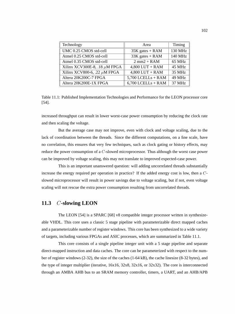
102
Technology Area Timing
UMC 0.25 CMOS std-cell 35K gates + RAM 130 MHzAtmel 0.25 CMOS std-cell 33K gates + RAM 140 MHzAtmel 0.35 CMOS std-cell 2 mm2 + RAM 65 MHzXilinx XCV300E-8, .18µM FPGA 4,800 LUT + RAM 45 MHzXilinx XCV800-6, .22µM FPGA 4,800 LUT + RAM 35 MHzAltera 20K200C-7 FPGA 5,700 LCELLs + RAM 49 MHzAltera 20K200E-1X FPGA 6,700 LCELLs + RAM 37 MHz
Table 11.1: Published Implementation Technologies and Performance for the LEON processor core[54].
increased throughput can result in lower worst-case power consumption by reducing the clock rate
and then scaling the voltage.
But the average case may not improve, even with clock and voltage scaling, due to the
lack of coordination between the threads. Since the different computations, on a fine scale, have
no correlation, this ensures that very few techniques, such as clock gating or history effects, may
reduce the power consumption of aC-slowed microprocessor. Thus although the worst case power
can be improved by voltage scaling, this may not translate to improved expected-case power.
This is an important unanswered question: will adding uncorrelated threads substantially
increase the energy required per operation in practice? If the added energy cost is low, then aC-
slowed microprocessor will result in power savings due to voltage scaling, but if not, even voltage
scaling will not rescue the extra power consumption resulting from uncorrelated threads.
11.3 C-slowing LEON
The LEON [54] is a SPARC [68] v8 compatible integer processor written in synthesize-
able VHDL. This core uses a classic 5 stage pipeline with parameterizable direct mapped caches
and a parameterizable number of register windows. This core has been synthesized to a wide variety
of targets, including various FPGAs and ASIC processes, which are summarized in Table 11.1.
This core consists of a single pipeline integer unit with a 5 stage pipeline and separate
direct-mapped instruction and data caches. The core can be parameterized with respect to the num-
ber of register windows (2-32), the size of the caches (1-64 kB), the cache linesize (8-32 bytes), and
the type of integer multiplier (iterative, 16x16, 32x8, 32x16, or 32x32). The core is interconnected
through an AMBA AHB bus to an SRAM memory controller, timers, a UART, and an AHB/APB

103
Instruction CyclesJMPL 2Double load 2Single store 2Double store 3SMUL/UMUL 1/2/4/35*SDIV/UDIV 35Taken Trap 4Atomic load/store 3All other instructions 1
Table 11.2: The latency for various instructions in the LEON pipeline [54].
bridge.
The Leon core used for benchmarking was modified to exclude the caches and external
logic. The register file was not manually increased, but had sufficient resources to hold teh additional
logic. Then the resulting design was passed through the automaticC-slow retiming tool described in
Chapter 13,1 with the resulting core nearly doubling in throughput for a2-slow version: increasing
in performance from 23 MHz without retiming to 46 MHz after 2-slowing and retiming. Since this
core excluded the caches and other logic, the costs of changing the external logic were not measured,
but only the effects on the core itself.
11.4 Summary
This chapter demonstrated the generality of theC-slow transformation and how it can
be applied to a highly complex design. If applied to a microprocessor core, an “Interleaved Mul-
tithreaded” architecture is created: offering higher throughput on multithreaded workloads by in-
creasing the pipelining. Only very minor architectural changes are required outside the changes
introduced by theC-slow transformation.
1More details on this process are described in Chapter 13.

104
Chapter 12
The Effects of Placement and Hand
C-slowing
The hand-mapped benchmarks: AES, Smith/Waterman, and the synthetic datapath, were
all implemented with hand placement and handC-slowing. Hand-placement enables later compar-
isons in Chapter 14 to exclude artifacts introduced by automatic placement, while handC-slowing
is used to calibrate the automatic tool described in Chapter 13.
Beyond providing designs for future study and comparisons, this can also be used to
evaluate the importance of both transformations and the quality of the Xilinx placement tools, by
removing the placement and additional retiming from the designs and comparing the resulting qual-
ity. Combining handC-slowing with hand-placement can more than double the throughput on some
designs.
Likewise, removing the placement from a design often degrades performace, illustrating
the tool sensitivity of designs targeting conventional FPGAs. This sensitivity is far less significant
with fixed-frequency arrays such as the SFRA, as will be seen in Chapter 14.
12.1 The Effects of Hand Placement andC-slow Retiming
Since hand-placement creates high quality datapaths and systolic structures appropriate
to both the design and target architecture, hand placements can be used to evaluate the placement
quality of automatic tools. In general, a good hand placement offers superior performance when
compared with current automatic placement tools which don’t exploit datapath regularity. It is
possible to create datapath placement tools [38, 15], but these techniques are currently not included
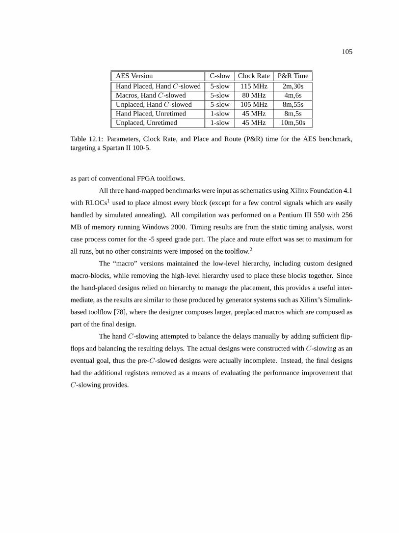
105
AES Version C-slow Clock Rate P&R Time
Hand Placed, HandC-slowed 5-slow 115 MHz 2m,30sMacros, HandC-slowed 5-slow 80 MHz 4m,6sUnplaced, HandC-slowed 5-slow 105 MHz 8m,55sHand Placed, Unretimed 1-slow 45 MHz 8m,5sUnplaced, Unretimed 1-slow 45 MHz 10m,50s
Table 12.1: Parameters, Clock Rate, and Place and Route (P&R) time for the AES benchmark,targeting a Spartan II 100-5.
as part of conventional FPGA toolflows.
All three hand-mapped benchmarks were input as schematics using Xilinx Foundation 4.1
with RLOCs1 used to place almost every block (except for a few control signals which are easily
handled by simulated annealing). All compilation was performed on a Pentium III 550 with 256
MB of memory running Windows 2000. Timing results are from the static timing analysis, worst
case process corner for the -5 speed grade part. The place and route effort was set to maximum for
all runs, but no other constraints were imposed on the toolflow.2
The “macro” versions maintained the low-level hierarchy, including custom designed
macro-blocks, while removing the high-level hierarchy used to place these blocks together. Since
the hand-placed designs relied on hierarchy to manage the placement, this provides a useful inter-
mediate, as the results are similar to those produced by generator systems such as Xilinx’s Simulink-
based toolflow [78], where the designer composes larger, preplaced macros which are composed as
part of the final design.
The handC-slowing attempted to balance the delays manually by adding sufficient flip-
flops and balancing the resulting delays. The actual designs were constructed withC-slowing as an
eventual goal, thus the pre-C-slowed designs were actually incomplete. Instead, the final designs
had the additional registers removed as a means of evaluating the performance improvement that
C-slowing provides.

106
AES Version C-slow Latency Bandwidth Area
Hand Placed, HandC-slowed 5-slow 480 ns 1.3 Gb/s 773 slices, 10 BlockRAMsMacros, HandC-slowed 5-slow 690 ns .930 Gb/s 805 slices, 10 BlockRAMsUnplaced, HandC-slowed 5-slow 520 ns 1.2 Gb/s 945 slices, 10 BlockRAMsHand Placed, Unretimed 1-slow 240 ns .520 Gb/s 461 slices, 10 BlockRAMsUnplaced, Unretimed 1-slow 240 ns .520 Gb/s 477 slices, 10 BlockRAMs
Table 12.2: Latency, Throughput, and area values for the AES benchmark, targeting a Spartan II100-5
12.2 AES Results
As can be seen in Table 12.1, the effect of C-slow retiming on AES performance is quite
significant. Even without datapath placement, it offers over 100 MHz performance and 1.2 Gbps
throughput, a 130% improvement in throughput at the cost of a 100% increase in area on the Spartan
II series of parts. The area cost needed for this additional throughput, although seemingly high, is
not really prohibitive as the initial design is limited by the availability of BlockRAMs to implement
the S-boxes, not the FPGA logic itself. Thus the additional resources represent otherwise unused
logic in this design.
This good showing for simulated annealing is to be expected, because although AES has a
large amount of structure when seen at the macro-level, the mixing nature of ciphers means that this
structure does not appear at the bit level, enabling conventional automatic placement to be effective.
Even so, datapath placement when added to C-slow retiming offers further increases in
performance (10%) and a significant reduction in area (20%). This is due to the more efficient pack-
ing which the datapath-placed version employs, with closely related (but seemingly independent)
logic packed together as well as guaranteeing that all registers were packed with associated LUT
outputs.3
In general, the heavily retimed versions for AES impose a significantly greater area over-
head than seen in the other benchmarks. This is largely because the design is BlockRAM limited,
1An RLOC is a placement directive, telling the Xilinx placement tool where a particular feature should be placed inthe FPGA.
2There exist well-known and directly observed deficiencies in the Xilinx ISE 4.1 router which require maximum effortto overcome, even when the router is provided with a high-quality, hand-placed datapath.
3The Xilinx mapping/packing tool, when the density is low, is very conservative about packing logic as the placementtool only operates on packed slices. If the mapper makes a bad decision and inappropriately packs unrelated logic, thiswill substantially degrade performance. Thus, when there are sufficient resources, the Xilinx packing tool tends to err onthe side of caution and avoids combining logic.

107
Smith/WatermanVersion C-slow Clock Rate P&R Time String Clock Area
Hand Placed,HandC-slowed 4-slow 100 MHz 3m,55s 25 MHz 1497 slicesUnplaced,HandC-slowed 4-slow 90 MHz 5m,20s 22.5 MHz 1530 slicesHand Placed,Unretimed 1-slow 45 MHz 2m,20s 45 MHz 1170 slicesUnplaced,Unretimed 1-slow 40 MHz 2m,50s 40 MHz 1112 slices
Table 12.3: Parameters, clock rate, and place and route time for the Smith/Waterman benchmark, 8cells, targeting a Spartan II-200-5
implying that LUTS are not the critical resource and therefore allowing more resources to be used
for retiming. Additionally, in order to minimize the critical path, both the BlockRAM inputs and
outputs are registered, adding 256 registers to the encryption core. A similar cost is needed for
the subkey generation, where 64 bits of registers are required to pipeline the memory access and
128 SRL16s are needed to balance out the delays in subkey generation. The placement distributes
the computation across the long cross-chip communications present in this design, with associated
pipelining to insure high clock rate.
Of greater concern is the poor performance shown when the toolflow is given a design
containing preplaced word-oriented macros but no higher level structure. Simulated annealing often
makes small mistakes when given a fairly highly utilized design, but these mistakes are considerably
magnified when given the 8-bit preplaced, primitive blocks used to compose the Rijndael implemen-
tation as minor vertical offsets are now magnified due to the larger blocks involved. A 20% decrease
in throughput is the result when compared to the version withall placement constraints removed!
12.3 Smith/Waterman results
Smith/Waterman (Table 12.3) shows a similar, impressive speedup between the retimed
and unretimed versions of 120%, but a much lower 30% penalty in area. The significantly lower
area overhead, when compared to the AES benchmark, is due to less aggressiveC-slowing which
is designed to match the structure of the computation.
If the design wasC-slowed more aggressively, the resulting design would have signifi-

108
DatapathVersion C-slow Clock Rate P&R Time Thread Clock Area
Hand Placed,HandC-slowed 3-slow 105 MHz 5m40s 35 MHz 415 slicesMacros,HandC-slowed 3-slow 105 MHz 7m40s 35 MHz 415 slicesUnplaced,HandC-slowed 3-slow 105 MHz 7m0s 35 MHz 404 slicesHand Placed,Unretimed 1-slow 55 MHz 5m50s 55 MHz 364 slicesUnplaced,Unretimed 1-slow 50 MHz 6m0s 50 MHz 365 slices
Table 12.4: Parameters, clock rate, and place and route time for the synthetic datapath, targeting aSpartan II-150-5
cantly higher area overhead, as most of the additional registers could not be packed into the existing
logic blocks. Since the design is a systolic computation and does not use any BlockRAMs, it is
critically important that the increased area not overtake the increased performance.
Similarly, the best clock cycle is close to the limit for a 16-bit adder. Without breaking the
carry chain and using a carry-select or pipelined-carry adder, it is effectively impossible to generate
a substantial increase in clock rate over the aggressivelyC-slowed version. Additionally, the Virtex
architecture can’t pipeline the carry-chain without crossing onto the more general interconnect,
which limits the benefit of pipelining small (< 16 bit) adders.
As before, removing the datapath placement constraints has a significant (10%-15%) per-
formance impact on the final design, as well as increasing place and route time, when compared
to the preplaced versions. There is no separate “macro” version, as the bulk of the design is com-
posed of adders which always retain relative placement information to comply with the constraints
imposed by the carry chain.
12.4 Synthetic Datapath Results
As in Smith/Waterman, the more limitedC-slowing of the synthetic datapath produced
significant performance benefits (90% improvement) while limiting the area impact (15% penalty)
and the latency penalty (35% penalty), as seen in Table??. Again, this is due to the limited nature
of theC-slowing, attempting to match the available resources in the design.

109
Of interest, however, is the limited effect of removing the datapath constraints on the
retimed version. In the case of the macroblock-based retimed version, simulated annealing appears
to have worked well because the placement problem becomes a 1-D packing problem rather than
a conventional 2-D placement problem due to the height of the macros compared with the size of
the chip. As a result, simulated annealing creates a mostly aligned datapath, and there are no severe
misalignments due to vertical stacking of components.
The pure simulated-annealing placement for the retimed datapath worked surprisingly
well due to the very fine nature of the placement problem, the comparatively low device utilization,
and the butterfly network effects (first noted by Singh in [65]), which apply to the layout of the
shifter representing a large portion of this design. Although simulated annealing does produce good
results for this benchmark, there is a natural increase in place and route time.
12.5 Summary
This chapter shows the significant effects of datapath placement andC-slow retiming on
the three hand-placed benchmarks. These transformations, when implemented by hand, can more
than double throughput, at a reasonable cost in area and latency. These benchmark implementations
will be used again in Chapter 13 to gauge the effectiveness of the automaticC-slow retiming tool
and in Chapter 14 to enable comparisons between the SFRA and the Xilinx Virtex.
110
Chapter 13
Automatically Applying C-Slow
Retiming to Xilinx FPGAs
Fixed Frequency FPGAs offer substantial improvements in throughput over conventional
FPGAs through fine-grained pipelining. In order to utilize the pipeline registers, repipelining or
C-slow retiming is essential. Yet as these transformations are applicable to conventional FPGAs, it
is important to separate the architectural benefits of Fixed Frequency operation from the throughput
gains fromC-slow retiming.
To quantify the effects ofC-slow retiming on real designs and to facilitate a direct compar-
ison between a proposed fixed-frequency architecture and a commercial FPGA, this thesis develops
a prototypeC-slow retiming tool that operates after placement, targeting the Xilinx Virtex [82] fam-
ily of FPGAs.1 This tool is deliberately simplistic, as it is designed simply to assess the costs and
benefits ofC-slow retiming when applied with minimal disruption to a commercial FPGA toolflow.
13.1 Retiming and the Xilinx Toolflow
The Xilinx toolflow operates in several stages: Synthesis or schematic capture, translation,
mapping, placement, routing, and static timing analysis. During synthesis, the design is converted
from an HDL representation to an output netlist. This netlist is translated to Xilinx.ngd format
for use by the remaining tools use. Mapping takes the logical elements (gates, flip-flops, and other
features), combining them into Xilinx slices. Once packed into slices, the packing is not modified
in the normal flow. Thus, when there are suitable resources available, the packing is deliberately1This line includes the Xilinx Virtex, Virtex E, Spartan II and Spartan II-E lines.
111
conservative, choosing to underutilize the array resources to avoid packing unrelated items in the
same slice. At high utilization, the packing tool will have no choice but to pack potentially unrelated
items.
After mapping, the placement tool places these slices in the array. Since the placement
tool operates on slices and larger macros, the presence of unrelated logic packed into a slice can
seriously disturb the results. Following placement, mapping attempts to minimize delays. Although
the process is formally complete after routing, several steps are still employed. Bit-generation
converts the design into a bitfile, which can be loaded into the array. Static timing analysis computes
the critical path, while back-annotation enables timing-accurate simulation.
Between mapping, placement, routing, and static timing analysis, designs are carried in an
.ncd binary format. In order to facilitate additional tools, Xilinx defines a text-based.xdl format
and a translator to convert between.xdl and.ncd . A minor limitation is that the.ncd format
does not include some user-imposed placement constraints, such asrloc origin 2 constraints.
By operating on the.xdl file format, it is possible to modify designs at any point in the
mapping, placement, routing, and timing analysis pathway. Arbitrary design modifications, as long
as they don’t create an invalid design, can be introduced into the design flow. The only limitations
are that significant changes will prevent backannotation from operating correctly, as backannotation
tracks design modifications through undocumented auxiliary files.
An important question is when to integrate the modifications into the toolflow: pre-
placement, post-placement, or post-routing. A decision was made to abandon the notion of modi-
fying the placement itself, as this introduces severe complications, while post-routing offers effec-
tively no benefits and would require either rerunning or replacing the routing process.
Because of the lack of designer placed constraints in the.xdl file, the placement tool
only operating on slices rather than elements, and the lack of good timing information before place-
ment, it was decided to perform all transformations after placement. If a tool desired pre-placement
retiming, the effects of packing flip-flops with unrelated logic would significantly skew the place-
ment and routing process.
This is especially important because the flip-flops in the Virtex slice can be used inde-
pendently of the logic through the BX and BY inputs under almost all cases. The only exceptions
are when the F5 or F6 muxes are used, when the LUT is used for routing, the LUTs are used as
memory devices, or when the carry-in is driven by external logic or a fixed constant. Yet because
2A means of specifying the absolute placement of design components.

112
SynplifyHDL Synthesis
Schematic
VHDL/Verilog
Xilinx VirtexTranslate & Map
ReplaceCEs
Xilinx VirtexPlacement
ResearchXilinx C-Slow
Xilinx VirtexRouting
Xilinx VirtexTiming Analysis
UnoptimizedXilinx Clock Rate
ResearchSFRA C-Slow
ResearchSFRA Router
Xilinx VirtexRouting
Xilinx VirtexTiming Analysis
OptimizedXilinx Clock Rate
ResearchSFRA C-Slow
SFRA FinalC-slow Factor
Figure 13.1: The complete toolflow created for this research. This section focuses on the Xilinxretiming tool, with its comparisons to the unoptimized Xilinx designs.
the placement tool operates on slices, flip-flops that are packed with unrelated logic will severely
impact placement quality.
13.2 An Automated C-Slow Tool for Virtex FPGAs
A modified toolflow was created as a series of perl scripts, used to invoke the Xilinx
synthesis, mapping, and placement tools, before converting the design to.xdl . This .xdl file is
loaded into a Java tool that performs the actualC-slowing and retiming. After retiming, the design
is converted back to.ncd before the Xilinx router and static timing analyzer are invoked. An
additional option allows the sameC-slow tool to target the SFRA, in conjunction with the SFRA
router. This toolflow uses maximum effort for the Xilinx tools, and is illustrated in Figure 13.1.
The tool first loads the design and ensures that it contains no features that would inhibit
C-slow retiming, such as clock enables, LUTs as RAM, SRL16s, or set/reset connections. Once
the design is verified, it is converted to a directed graph that represents the retiming problem. All
registers in the design are removed and replaced with edge weights, allowing them to be freely
moved. BlockRAMs and I/O pad registers are likewise removed and replaced with mandatory
constraints. Any negative-edge clocked memories are changed to operate on a positive clock, with
113
constraints to insure that registers will be placed on the outputs.
The tool creates estimates of logic and interconnect delay. Logic delays are based on
the published datasheet numbers for LUT evaluation, BlockRAM evaluation, carry chain costs, and
other architectural features. For estimating interconnect delay, the tool uses a simple Manhattan
distance metric that abstracts out the different interconnect types, using a linear cost model based
on an initial cost and then an extension cost. This cost-model was derived from a combination of
Xilinx datasheet timings and empirical experimentation. Once the tool creates a final cost estimate
for all components in a design, the design can then beC-slowed by simply multiplying the number
of registers on any given edge by the specifiedC. If only retiming is desired,C is simply set to 1.
Now having loaded the design and estimated all delays, the tool performs classical re-
timing with no regard to limiting the number of resulting registers or other constraints. This first
requires aO(V 3) operation3 to enumerate all possible critical paths in the design and the number of
registers currently along each such path, creating theW andD matrices which hold these values.
This also requiresO(n2) memory to store these matrices.
The next step involves determining the shortest critical path that the design can be retimed
to meet. This process uses a binary search to find the lowest critical path possible. Determining
whether a particular critical path can be achieved, the local constraints global constraints to ensure
that all longer paths are registered. The local constraints will ensure that there are no “negative”
registers on any link and that the number of registers around every path in the design remains
unchanged. Since all constraints are inequalities, the Bellman/Ford shortest-path algorithm is used,
anO(V 2) operation. The binary search iterates 10 times in order to find the best solution.
There are several minor techniques that speed up this process. If a solution exists, the
Bellman/Ford algorithm quickly converges, allowing us to perform far fewer iterations than are
required to guarantee convergence. Instead of performing theV iterations,V/20 appears highly
effective as even on the larger benchmarks. If a solution exists, it is discovered in few iterations even
on the most complex benchmark used. Additionally, if a solution is discovered, future iterations will
not change. Thus the tool detects if a solution is found and stop the process after a single additional
iteration where no changes occur. This offers a huge performance boost, reducing the overall cost
of the constraint solver by nearly50%.
An additional tweak involves carrying over the attempted solution from the last run. Since
this is either a correct solution for slightly more relaxed constraints or a mostly-correct solution for
3This could be replaced with anO(V 2 lg V ) step, but would necessitate changing the representations used
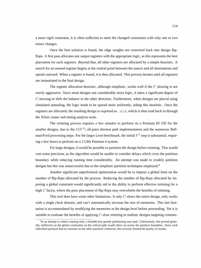
114
a more rigid constraint, it is often sufficient to meet the changed constraints with only one or two
minor changes.
Once the best solution is found, the edge weights are converted back into design flip-
flops. A first pass allocates any output registers with the appropriate logic, as this represents the best
placement for such registers. Beyond that, all other registers are allocated by a simple heuristic. A
search for an unused register begins at the central point between the source and all destinations and
spirals outward. When a register is found, it is then allocated. This process iterates until all registers
are instantiated in the final design.
The register allocation heuristic, although simplistic, works well if theC slowing is not
overly aggressive. Since most designs use considerably more logic, it takes a significant degree of
C-slowing to shift the balance in the other direction. Furthermore, when designs are placed using
simulated annealing, the logic tends to be spread more uniformly, aiding this heuristic. Once the
registers are allocated, the resulting design is exported as.xld , which is then read back in through
the Xilinx router and timing analysis tools.
The retiming process requires a few minutes to perform on a Pentium III 550 for the
smaller designs, due to theO(V 3) all-pairs shortest path implementation and the numerous Bell-
man/Ford processing steps. For the larger Leon benchmark, the initialV 3 step is substantial, requir-
ing a few hours to perform on a 2 GHz Pentium 4 system.
For large designs, it would be possible to partition the design before retiming. This would
cost some precision, as the algorithm would be unable to consider delays which cross the partition
boundary while reducing running time considerably. An attempt was made to crudely partition
designs but this was unsuccessful due to the simplistic partition techniques employed.4
Another significant unperformed optimization would be to impose a global limit on the
number of flip-flops allocated by the process. Reducing the number of flip-flops allocated by im-
posing a global constraint would significantly aid in the ability to perform effective retiming for a
highC factor, where the poor placement of flip-flops may overwhelm the benefits of retiming.
This tool does have some other limitations. It onlyC-slows the entire design, only works
with a single clock domain, and can’t automatically increase the size of memories. This last limi-
tation is accommodated by modifying the memories at the design level before proceeding. Yet it is
suitable to evaluate the benefits of applyingC-slow retiming to realistic designs targeting commer-
4In an attempt to reduce running time, a breadth-first greedy partitioning was used. Unfortuntaly, this proved gener-ally ineffective as the global constraints on the critical path would often cut across the partition boundries. Since eachindividual partition had no estimate on the other partition’s behavior, this severely limited the quality of results.
115
Figure 13.2:C-slowing and retiming all the benchmarks and the effects on throughput and latency.A C-slow factor of 1 just performs retiming. Throughput is substantially improved, roughly dou-bling the throughput in the best case. As expected,C-slowing does increase the latency for a singlecomputation.
cial FPGAs, and demonstrates that throughputs can be substantially increased by using automated
C-slow retiming tools.
13.3 Results
In order to evaluate the quality of results, this tool was applied to all four application-based
benchmarks described in Chapter 3 targeting various members of the Xilinx Virtex [82] family of
FPGAs. All were placed and routed using Xilinx Foundation 4.1i with maximum effort. All timings
are reported by the Xilinx static timing analysis tool. For the hand-placed benchmarks, the results
of the automatic tool are compared with the careful hand-constructed retimings to verify the quality
of this tool.
Figure 13.2 graphically depicts the effects on all benchmarks. Just retiming (aC-slow
factor of one) offers only a small amount of benefit, while more agressiveC-slowing can increase the
throughput substantially. In most cases, the optimumC-slow factor for a given benchmark nearly
doubles the throughput. For all benchmarks, there comes a point where additionalC-slowing offers
little or no benefit. Naturally, this increase in throughput also degrades latency, with the equivelent
clock rate for a single stream of execution substantially worsened.
More details and the results for the individual benchmarks are presented in the following

116
Version LUT Associated LUT Unassociated Clock Stream ClockFlip Flops Flip Flops MHz MHz
None 48 MHz 48 MHz5-slow by hand 105 MHz 21 MHz
Retimed automatically 150 0 47 MHz 47 MHz2-slow automatically 302 289 64 MHz 32 MHz3-slow automatically 348 668 75 MHz 25 MHz4-slow automatically 447 899 87 MHz 21 MHz5-slow automatically 462 1324 88 MHz 18 MHz
Table 13.1: The effects of C-slow retiming the AES encryption core placed with simulated anneal-ing on a Spartan II 100. This tool produces highly competitive results, able to nearly double thethroughput using automated transformations.
Version LUT Associated LUT Independent Clock Stream ClockFlip Flops Flip Flops MHz MHz
None 48 MHz 48 MHz5-slow by hand 115 MHz 23 MHz
Retimed automatically 132 37 50 MHz 50 MHz2-slow automatically 332 110 74 MHz 37 MHz3-slow automatically 404 515 95 MHz 32 MHz4-slow automatically 660 459 86 MHz 22 MHz5-slow automatically 660 885 105 MHz 21 MHz
Table 13.2: The effects of C-slow retiming the hand placed AES encryption core targeting a SpartanII 100. For 5-slow retiming, the throughput more than doubled when compared with the original,unretimed version.
subsections.
13.3.1 AES Encryption
For testing purposes, the process began with AES implementation that was hand placed
and hand retimed 5-slow to operate at 115 MHz on a Spartan 2 100, speedgrade 5. Removing the
placement information reduces the clock to 105 MHz, while removing both placement and retiming
information reduces the clock to 48 MHz. This design requires 10 BlockRAMs and about 800
LUTs. Experiments were performed on both the simulated annealing and hand placed versions,
comparing the automated results ofC-slowing with the manual results for both hand-placed and
automatically-placed versions. Table 13.1 shows the effects ofC-slow retiming on the design when
117
automated placement is used. Table 13.2 shows the benefits for a hand placed design.
The tool reports both the number of flip-flops that are bundled with associated logic and
the number that have to be scavenged from unused elements of the FPGA for this automatic tool. In
any case, this design is BlockRAM, not LUT limited, so large numbers of registers can be allocated
without an area penalty. The clock rate represents the total throughput of the system, while the
stream clock is the latency for any single task or stream of execution (simply the clock rate divided
by theC-slow factor). AggressiveC-slowing increases overall throughput for multiple execution
streams at the cost of single thread latency.
For both cases, although the results are still somewhat inferior to the hand-crafted imple-
mentations, they are highly competitive, with throughput more than doubling for the hand placed,
5-slow version. As expected, retiming withoutC-slowing provides negligible benefit, as the critical
path is defined by a single cycle feedback loop.
The limitations on the tool for a highC factor are due to an inability to alter the logic
placement in response to the numerous registers that need to be added and the simple heuristic used
to allocate the flip flops. The hand-placed version contains a subkey generation module, expressing
roughly 1/3 of the interconnect in 1/5 of the FPGA area. This poses significant difficulties for the
tool when allocating large numbers of flip-flops. Additionally, the hand-created implementations
used SRL16s to create a compact 128b wide, 3 cycle long delay chain in the subkey generation
core, a technique not employed by this tool. This creates an enormous amount of pressure on the
retiming tool, which has to add approximatly 512 registers (for 5-slow operation) into the subkey
generation module, yet that module is in a region of the chip containing only 480 flip-flops.
There are other factors that affect the resulting quality. The heuristics to calculate in-
terconnect delay are simply linear functions of Manhattan distance and don’t capture the costs of
various interconnect types, and the procedures for allocating flip flops are comparatively crude.
Additionally, theC-slow retiming process needs to allocate a considerable number of registers, be-
cause even at the highest level, there are 256 bits of datapath which requireC-slowing. Even the best
case, using an omnicient tool capable of restructuring the implementation, a5-slow implementation
would require allocating over 1000 registers throughout the design.
One particular point of interest is the 4-slow case for hand placement. WhenC-slowing,
the latency for each thread is always worse, with the hope that the total throughput increases. It
is not fully understood why the change from 3-slow to 4-slow reduces the throughput, while the
transition from 4-slow to 5-slow increases it. This probably involves poor heuristics used to allocate
new flip-flops that do not occur in the 5-slow case but are apparent in the 4-slow version, as these

118
C-slow LUT Associated LUT Unassociated Clock Stream ClockFactor Flip Flops Flip Flops MHz MHz
None 43 MHz 43 MHz4-slow by hand 90 MHz 22 MHz
Retimed automatically 628 287 40 MHz 40 MHz2-slow automatically 762 1010 69 MHz 34 MHz3-slow automatically 811 1723 84 MHz 28 MHz4-slow automatically 832 2524 76 MHz 25 MHz
Table 13.3: The effects of C-slow retiming on the Smith/Waterman Implementation, for simulatedannealing placement on a Spartan II 200. The 3 slow version almost doubles the throughput, whilethe automatic 4 slow version has passed the point of diminishing returns due to the large number offlip flops that required allocation.
C-slow LUT Associated LUT Unassociated Clock Stream ClockFactor Flip Flops Flip Flops MHz MHz
Original 45 MHz 45 MHz4-slow by hand 100 MHz 25 MHz
Retimed automatically 555 321 41 MHz 41 MHz2-slow automatically 813 972 57 MHz 29 MHz3-slow automatically 752 1167 86 MHz 28 MHz
Table 13.4: The effects of C-slow retiming on the Smith/Waterman Implementation for hand place-ment on a Spartan II 200. Again, a highC factor nearly doubles the throughput.
heuristics are designed to place individual flip flops rather than the longer chains of flip-flops which
are needed in the subkey-generation module. The hand-placed version is particularly difficult for
the automated tool, as 1/2 of the dataflow (the subkey generation) is confined to 1/5th of the FPGA,
yet requires nearly as many registers.
13.3.2 Smith/Waterman
A hand mapped, placed, and hand retimed 4-slow Smith/Waterman cell was utilized, able
to operate at 100 MHz on a Spartan II 200. This cell uses a 5 bit alphabet, 5 bit costs, affine gap
distance, and 16 bit arithmetic quantities, with the string being matched against compiled into the
configuration. Removing the placement information reduces the clock to 90 MHz. Removing both
placement and retiming information reduces the clock to 44 MHz. This design requires about 1700
LUTs, of which most are adders.

119
C-slow LUT Associated LUT Unassociated Clock Thread ClockFactor Flip Flops Flip Flops MHz MHz
None 51 MHz 51 MHz3-slow by hand 105 MHz 35 MHz
Retimed automatically 201 96 54 MHz 54 MHz2-slow automatically 294 284 86 MHz 43 MHz3-slow automatically 326 470 91 MHz 30 MHz4-slow automatically 326 779 82 MHz 20 MHz
Table 13.5: The effects of C-slow retiming on the synthetic microprocessor core targeting a SpartanII 150-5, placed with simulated annealing.
C-slow LUT Associated LUT Unassociated Clock Thread ClockFactor Flip Flops Flip Flops MHz MHz
None 55 MHz 55 MHz3-slow by hand 105 MHz 35 MHz
Retimed automatically 165 37 59 MHz 59 MHz2-slow automatically 238 281 85 MHz 43 MHz3-slow automatically 289 501 88 MHz 29 MHz4-slow automatically 289 830 88 MHz 22 MHz
Table 13.6: The effects of C-slow retiming on the hand placed synthetic microprocessor datapathtargeting a Spartan II 150-5
The results are summarized in Table 13.3 and Table 13.4. The slight performance decrease
for retiming withoutC-slowing is due to imprecision in the delay-modeling that resulted in some
slightly poor decisions. Again, this design is limited by a single-cycle feedback loop, so retiming
without C-slowing was not expected to be beneficial. Beyond that,C-slow retiming shows the
expected performance gains, with not quite double the throughput for the3-slow, automatically
placed version at 84 MHz.
The tool was deliberately conservative: never using an unrelated flip-flop when the carry
chain was used, instead of being slightly more selective by monitoring the carry-in state. This
is a fairly significant restriction on the Smith/Waterman benchmark as the design consists almost
entirely of adders and multiplexors, yet the tool still produces effective results.
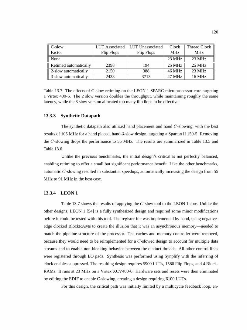
120
C-slow LUT Associated LUT Unassociated Clock Thread ClockFactor Flip Flops Flip Flops MHz MHz
None 23 MHz 23 MHz
Retimed automatically 2398 194 25 MHz 25 MHz2-slow automatically 2150 388 46 MHz 23 MHz3-slow automatically 2438 3713 47 MHz 16 MHz
Table 13.7: The effects of C-slow retiming on the LEON 1 SPARC microprocessor core targetinga Virtex 400-6. The 2 slow version doubles the throughput, while maintaining roughly the samelatency, while the 3 slow version allocated too many flip flops to be effective.
13.3.3 Synthetic Datapath
The synthetic datapath also utilized hand placement and handC-slowing, with the best
results of 105 MHz for a hand placed, hand-3-slow design, targeting a Spartan II 150-5. Removing
the C-slowing drops the performance to 55 MHz. The results are summarized in Table 13.5 and
Table 13.6.
Unlike the previous benchmarks, the initial design’s critical is not perfectly balanced,
enabling retiming to offer a small but significant performance benefit. Like the other benchmarks,
automaticC-slowing resulted in substantial speedups, automatically increasing the design from 55
MHz to 91 MHz in the best case.
13.3.4 LEON 1
Table 13.7 shows the results of applying theC-slow tool to the LEON 1 core. Unlike the
other designs, LEON 1 [54] is a fully synthesized design and required some minor modifications
before it could be tested with this tool. The register file was implemented by hand, using negative-
edge clocked BlockRAMs to create the illusion that it was an asynchronous memory—needed to
match the pipeline structure of the processor. The caches and memory controller were removed,
because they would need to be reimplemented for aC-slowed design to account for multiple data
streams and to enable non-blocking behavior between the distinct threads. All other control lines
were registered through I/O pads. Synthesis was performed using Synplify with the inferring of
clock enables suppressed. The resulting design requires 5900 LUTs, 1580 Flip Flops, and 4 Block-
RAMs. It runs at 23 MHz on a Virtex XCV400-6. Hardware sets and resets were then eliminated
by editing the EDIF to enable C-slowing, creating a design requiring 6100 LUTs.
For this design, the critical path was initially limited by a multicycle feedback loop, en-
121
abling conventional retiming to offer a limited benefit. Conventional retiming also eliminated the
fragmented cycle from the memory access by converting the BlockRAM to positive-edge clocking
and forcing the design to rebalance itself, offering a potential improvement in clock rate.
2-slow retiming showed a highly significant performance increase. LEON contains a
higher ratio of logic to pipeline registers when compared to the other benchmarks, implying that the
latency penalties for retiming would be comparatively lower. This situation the best possible case,
where the combined benefits of retiming andC-slowing produced a design where single threaded
throughput remains constant but aggregate throughput was doubled.
3-slow retiming attempted to allocate too many registers to create an efficient design,
resulting in such a marginal performance increase as to be negligible. This limitation suggests that
future work on better heuristics to limit flip-flop creating and improving allocation would provide
considerable benefits.
13.4 Architectural Recommendations for the Xilinx
It is possible to improve the Xilinx architecture to allow this tool to operate more ef-
fectively. Most limitations were discovered when aggressiveC-slowing was used, and therefore
many registers were required. It is possible to add 2 registers to the CLB without increasing I/O
requirements, if the registers lack the clock enable and reset functionality.
SinceC-slowing needs to use logic to implement set and clock enable functionality, these
inputs are no longer needed for such designs. By driving two new registers from the CE and SR
inputs, it becomes possible to use 4 registers forC-slowing. Likewise, these new registers can
drive the XB and YB outputs, signals which are only used to tap the carry chain and for occasional
CLB-routing purposes.
This would not improve the mildlyC-slowed designs, where almost no flip-flops need
to be scavanged, but should offer a significant gain on the agressivelyC-slowed designs, when
considerably more flip-flops need to be allocated. The final performance was limited by the flip-
flop allocation, not theC-slowing itself.
13.5 Retiming for the SFRA
In addition to retiming designs targeting the Xilinx Virtex, this tool also provides for the
fixed-frequency retiming used with the SFRA. As detailed in Section 10.5, fixed-frequency retiming

122
only requires local constraints, and rather than iterating to find a minimum critical path for a given
C, the process iterates to find the minimumC which meets all constraints.
Since the SFRA operates on the same design, and uses the same CLB layout, the same
retiming tool is used to target both architectures. The only difference is the SFRA retiming tool is
run twice, once before routing (using an approximate delay model) and once after routing (using
the final delays produced by routing).
13.6 Summary
This chapter describes a tool for automatically improving the performance of Xilinx de-
signs throughC-slowing and retiming. This tool was evaluated on the four benchmarks used
throughout this thesis, and directly compared with hand implementations to verify the quality of
the results. In many cases, throughput can be more than doubled using this tool.
This tool was evaluated on four benchmarks, three which contained handC-slowed ver-
sions. Although not quite matching the quality of handC-slowing, the automatic tool provides
significant performance gains. Even a highly complex, synthesized design like the LEON Sparc
core showed large improvements, doubling in throughput!

123
Part III
Comparisons, Reflections and
Conclusions

124
The final part of this thesis presents a comprehensive comparison between the SFRA and
the Xilinx Virtex, an analysis of the overall suitability of the fixed-frequency approach, the open-
questions remaining with the SFRA and corner-turn architectures, and a final conclusions.
Chapter 14 directly compares the SFRA with the Xilinx Virtex. For the same design, the
SFRA routing algorithms are an order of magnitude faster, as are the SFRA retiming algorithms.
Because of its pipelined, fixed-frequency nature, designs can run at significantly higher throughput
when compared to the Virtex.
Chapter 15 discusses the tradeoff between latency and throughput. In general, fixed-
frequency FPGAs offer higher throughput, but at the cost of substantially increased latency. On
throughput-bound applications, this is an acceptable tradeoff, but significantly degrades perfor-
mance on latency bound applications.
Chapter 16 discusses the remaining open questions. The first is the interaction between
power consumption andC-slowing, as there are complicated second-order effects which haven’t
been analyzed. The second is the interaction between the corner-turn topology and coarser-grained
FPGAs. In this area, corner-turning should be more efficient. The final open-question is the effect on
depopulating the C-boxes in a corner-turn array, and whether this could be done without adversely
affecting routability.
Chapter 17 summarizes this thesis, acting as an overall conclusion. It reviews the major
results, and includes an evaluation of both what was effective and what is less effective in the thesis
results.
125
Chapter 14
Comparing the SFRA with the Xilinx
Virtex
In order to provide quantitative comparisons between the Virtex and SFRA architectures,
the benchmarks discussed in Chapter 3 were mapped to both architectures. This chapter compares
the results of mapping the benchmark designs, with a focus on the differences in toolflow time,
design throughput, throughput normalized to area, and latency.
Not only does this chapter compare the SFRA with a commercial FPGA (the Xilinx Vir-
tex), but also compares the SFRA with the Virtex after the Virtex designs are improved through
automatic C-slowing (as described in Chapter 13).
14.1 Benchmark Designs
The benchmarks used for this comparison, AES encryption, Smith/Waterman sequence
matching, the synthetic datapath, and the LEON 1 microprocessor core, are described in detail in
Chapter 3 and Appendix A.
The AES and Smith/Waterman designs are both heavily optimized for the Virtex archi-
tecture. These applications are very appropriate for aggressiveC-slowing, as most usages attempt
to optimize throughput, not latency. Both benchmarks were hand-mapped, with both hand-placed
and automatically placed versions. Thus it is possible to differentiate between placement either by
hand or through simulated annealing and the subsequent effects on the router. The two benchmarks
stress different aspects, as AES uses bitwise operations and table lookups while Smith/Waterman is
almost entirely 16-bit arithmetic operations.
126
The synthetic datapath and the LEON 1 microprocessor core represent designs selected
for their datapath nature rather than their appropriateness for aggressiveC-slowing.1 Both designs
stress datapath functionality, although they are generated using different techniques. The synthetic
datapath is a carefully implemented, hand constructed design with both hand and automatically-
placed versions, while LEON 1 is fully synthesized and contains a large mix of control logic as well
as datapath. Being over 6000 LUTs, LEON 1 is a very substantial design.
Although the synthetic datapath and LEON 1 are not generally appropriate candidates
for aggressiveC-slow retiming, the datapath nature is a common construction which appears in
many applications, including image processing and other tasks, which do benefit from aggressive
C-slowing.
All these benchmarks were also accelerated using theC-slow tool discussed in Chap-
ter 13. Thus the comparisons don’t simply include unmodified Xilinx designs but Xilinx designs
which were accelerated using the same technique, fine-grained pipelining throughC-slowing, which
enables the SFRA to achieve high throughput.
14.2 The SFRA Target
The SFRA architecture, described in more detail in Chapter 5, uses a 120 wire routing
channel, fully populated C-boxes, and 2 turns in addition to the BX/BY inputs, for an effectively 6
turn array. All wires are broken every 3 CLBs with a bidirectional buffer, and every 9 CLBs they are
registered. The carry chain is registered every 4 CLBs (8 bits). All BlockRAM access is pipelined,
requiring 3 cycles.
As described in more detail in Chapter 5, the SFRA should be able to operate at at least
300 MHz in a .18 micron process based on simulating the critical path within the interconnect. This
timing estimate is used to specify the SFRA’s performance on this target architecture. Likewise,
the SFRA appears to be about 3.9 times larger than the Virtex, as the interconnect’s connectivity is
significantly richer.
14.3 The Xilinx Target
The Xilinx designs in Chapters 3 and 13 were mapped to the .22µm Spartan II and Virtex
architectures. As the .18µm Virtex E and Spartan IIe architectures have different BlockRAM
1Chapter 11 discusses how a minor degree ofC-slowing can accelerate a microprocessor core.
127
locations, this incompatibility prevents theC-slowing tool and the SFRA router from operating
properly. Additionally, upgrading the toolflow from 4.1 to the latest version, necessary to support
the Spartan IIe, would pose compatibility problems as the Foundation 5.1xdl tool will not accept
designs produced by the automaticC-slowing tool.
Instead, the Xilinx clock-rates are scaled to the .18µm process to account for the per-
formance difference. In Appendix A, the AES design was modified to account for the different
placement parameters and targeted at both the Spartan II (implemented in a .22µm process) and
the Virtex-E (implemented in the .18µm process). The resulting design improved from 115 MHz
to 155 MHz, an increase of 35%. To be conservative, a performance improvement of 40% is as-
sumed throughout the rest of this chapter. Table 14.1 summarizes the adjusted clock rates for all the
benchmark designs and parameters.
14.4 Toolflow Comparisons
All these benchmarks were placed using the Xilinx placement tools (version 4.1) with
maximum effort selected. The Xilinx router times are for maximum effort, as there are performance
drawbacks when lower effort is used. To provide an effective comparison, these benchmarks were
also retimed using the retiming tool developed for the Virtex. This tool can effectively double the
throughput on the benchmarks when targeting the Xilinx Virtex, and compares well with hand-
retiming. Thus the comparisons aren’t only with what the Xilinx toolflow currently supports, but
also potential improvements. All tools were run on a 550-MHz Pentium III with 256 MB of memory
running Windows 2000. The same placements are used for both the Virtex and SFRA targets.
The toolflow times for both architectures are summarized in Table 14.2. Thanks to the
polynomial-time heuristics, the SFRA router is one to two orders of magnitude faster than the Xilinx
router. This is despite the considerable effort Xilinx devotes to minimizing router run-time, while
the SFRA router is coded in straightforward Java with little care to optimizing performance.
It is impossible to directly compare router “quality”, as the SFRA and Xilinx routers have
vastly different targets. The SFRA router does minimize turn use and wire length, so the resulting
routes are minimum cost and nearly minimum delay.
Both retiming implementations, the SFRA retiming tool and the Xilinx retiming tool, are
simply two execution options within the same code base. The SFRA retiming is not reported in
isolation, but simply recoded as the combined toolflow time which includes data-loading, routing,
and the two retiming passes. Since most of the time involves retiming, this number reflects the cost
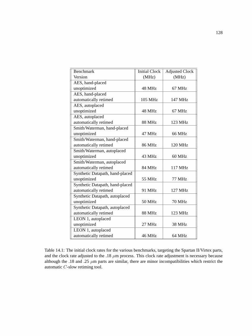
128
Benchmark Initial Clock Adjusted ClockVersion (MHz) (MHz)AES, hand-placedunoptimized 48 MHz 67 MHzAES, hand-placedautomatically retimed 105 MHz 147 MHzAES, autoplacedunoptimized 48 MHz 67 MHzAES, autoplacedautomatically retimed 88 MHz 123 MHzSmith/Waterman, hand-placedunoptimized 47 MHz 66 MHzSmith/Waterman, hand-placedautomatically retimed 86 MHz 120 MHzSmith/Waterman, autoplacedunoptimized 43 MHz 60 MHzSmith/Waterman, autoplacedautomatically retimed 84 MHz 117 MHzSynthetic Datapath, hand-placedunoptimized 55 MHz 77 MHzSynthetic Datapath, hand-placedautomatically retimed 91 MHz 127 MHzSynthetic Datapath, autoplacedunoptimized 50 MHz 70 MHzSynthetic Datapath, autoplacedautomatically retimed 88 MHz 123 MHzLEON 1, autoplacedunoptimized 27 MHz 38 MHzLEON 1, autoplacedautomatically retimed 46 MHz 64 MHz
Table 14.1: The initial clock rates for the various benchmarks, targeting the Spartan II/Virtex parts,and the clock rate adjusted to the .18µm process. This clock rate adjustment is necessary becausealthough the .18 and .25µm parts are similar, there are minor incompatibilities which restrict theautomaticC-slow retiming tool.
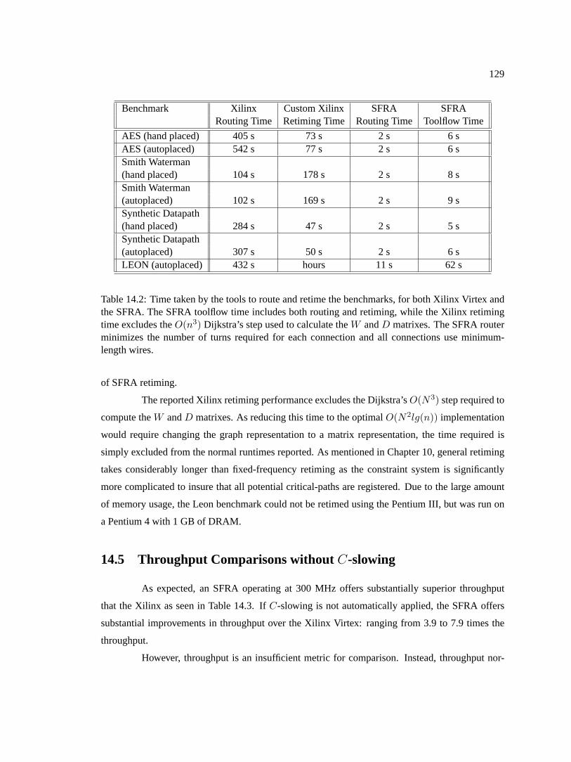
129
Benchmark Xilinx Custom Xilinx SFRA SFRARouting Time Retiming Time Routing Time Toolflow Time
AES (hand placed) 405 s 73 s 2 s 6 sAES (autoplaced) 542 s 77 s 2 s 6 sSmith Waterman(hand placed) 104 s 178 s 2 s 8 sSmith Waterman(autoplaced) 102 s 169 s 2 s 9 sSynthetic Datapath(hand placed) 284 s 47 s 2 s 5 sSynthetic Datapath(autoplaced) 307 s 50 s 2 s 6 sLEON (autoplaced) 432 s hours 11 s 62 s
Table 14.2: Time taken by the tools to route and retime the benchmarks, for both Xilinx Virtex andthe SFRA. The SFRA toolflow time includes both routing and retiming, while the Xilinx retimingtime excludes theO(n3) Dijkstra’s step used to calculate theW andD matrixes. The SFRA routerminimizes the number of turns required for each connection and all connections use minimum-length wires.
of SFRA retiming.
The reported Xilinx retiming performance excludes the Dijkstra’sO(N3) step required to
compute theW andD matrixes. As reducing this time to the optimalO(N2lg(n)) implementation
would require changing the graph representation to a matrix representation, the time required is
simply excluded from the normal runtimes reported. As mentioned in Chapter 10, general retiming
takes considerably longer than fixed-frequency retiming as the constraint system is significantly
more complicated to insure that all potential critical-paths are registered. Due to the large amount
of memory usage, the Leon benchmark could not be retimed using the Pentium III, but was run on
a Pentium 4 with 1 GB of DRAM.
14.5 Throughput Comparisons withoutC-slowing
As expected, an SFRA operating at 300 MHz offers substantially superior throughput
that the Xilinx as seen in Table 14.3. IfC-slowing is not automatically applied, the SFRA offers
substantial improvements in throughput over the Xilinx Virtex: ranging from 3.9 to 7.9 times the
throughput.
However, throughput is an insufficient metric for comparison. Instead, throughput nor-

130
Benchmark Adjusted Xilinx SFRA Expected Speedup AreaClock Rate C-slow for 300 MHz Normalized
(MHz) Factor SFRA Speedup
AES (hand placed) 67 MHz 24 slow 4.4x 1.1xAES (autoplaced) 67 MHz 27 slow 4.4x 1.1xSmith/Waterman(hand placed) 66 MHz 31 slow 4.4x 1.1xSmith/Waterman(autoplaced) 60 MHz 37 slow 5.0x 1.3xSynthetic Datapath(hand placed) 77 MHz 21 slow 3.9x 1.0xSynthetic Datapath(autoplaced) 70 MHz 23 slow 4.2x 1.1xLEON (autoplaced) 38 MHz 67 slow 7.9x 2.2x
Table 14.3: Throughput and Throughput/Area results for the unoptimized Virtex benchmarks whencompared with an 300 MHz SFRA.
malized to area is a better metric. As the Virtex architecture requires 42000µm2 per CLB, while
the SFRA requires 160000µm2 for the same amount of logic, resulting throughput is divided by
3.9 (the area ratio) to obtain an area normalized throughput.
This normalization is required as any application which can benefit fromC-slowing can
also have its throughput increased through replication, as the prerequisites forC-slowing a design
can also be matched through replication.
Nevertheless, the SFRA is competitive with the Xilinx Virtex, as the increased area is
countered by the greater throughput. On all benchmarks, the SFRA meets or exceeds (by up to a
factor of 2) the Xilinx throughput, even after area normalization. This is considered a highly positive
result, as the SFRA is a single-person effort while the Virtex is a 5th generation commercial product
from a highly successful company.
Additionally, the SFRA’s interconnect style is more appropriate to a coarse-grained archi-
tecture, but as there has been no commercially successful coarse-grained FPGA, this interconnect
topology must be compared at a less efficient point in the design space.
Another area of interest is the slightly greater sensitivity of the SFRA to poor placement,
but only in terms of latency. AES, although regular when viewed at a macro level, is composed
of highly irregular bit-mixing operations, preventing the SFRA from significantly benefiting from
a hand-placed datapath. Thus both versions, hand placed and automatically placed, show similar
131
performance.
Smith/Waterman, on the other hand, is composed of aligned arithmetic operations. With
automatic placement, the cumulative effect of small misalignments becomes substantial throughout
the feedback loop, while the hand-placed version insures that all dataflow is carefully aligned. Thus
the latency required is significantly larger for the automatically placed version.
Even so, although the Xilinx placer is not optimized for the SFRA architecture, it does a
respectable although not remarkable job when placing designs for this different interconnect. The
general success of the Xilinx placement tool is probably due to the timing domains which result
from a Hex-line based interconnect structure. Although Xilinx does not provide a great detail on the
timing domains produced, the resulting domains of a Virtex prototype which uses length 8 instead
of length 6 segmented wires is well described in [52].
For the Xilinx Hexline/Octline style of interconnect, the direct horizontal and vertical
alignments are the fastest, followed by the group offset around the point. Thus the cost for a slight
offset is significantly more than direct alignment, but the cost of a larger offset is not substantially
greater. This generally matches the SFRA architecture, although the penalties are different.
However, both automatically placed and manually placed designs targeting the SFRA
have the same throughput if fullC-slowing is acceptable. On a conventional FPGA such as the Vir-
tex, a bad placement will reduce both latency and throughput. Yet on a fixed-frequency architecture,
a bad placement only affects latency, not throughput, as the throughput is an intrinsic property of
the target architecture if suitable parallelism is exploited.
This is a key distinction between a conventional FPGA and a fixed-frequency FPGA. A
poor placement on the Xilinx both reduces throughput and increases latency. Yet the SFRA, like
any other fixed-frequency architecture supportingC-slowing, will only show increased latency. So
although automatically-placed benchmarks are not as effectively mapped to the SFRA, the relative
throughput improvement over the Xilinx is increased when both arrays have designs with suboptimal
placement.
14.6 Throughput Comparisons withC-slowing
Naturally, much of the SFRA’s benefits derive from theC-slowing transformation itself.
By using the tool described in Chapter 13 to improve the quality of Xilinx designs, it is possible to
separate the benefits ofC-slowing from the benefits of fixed-frequency operation. These results are
summarized in Table 14.4.

132
Benchmark Adjusted Xilinx SFRA Expected Speedup AreaClock Rate C-slow for 300 MHz Normalized
(MHz) Factor SFRA Speedup
AES (hand placed) 147 MHz 5-slow 24 slow 2.0x .5xAES (autoplaced) 123 MHz 5-slow 27 slow 2.4x .6xSmith/Waterman(hand placed) 120 MHz 3-slow 31 slow 2.5x .6xSmith/Waterman(autoplaced) 117 MHz 3-slow 37 slow 2.5x .6xSynthetic Datapath(hand placed) 127 MHz 3-slow 21 slow 2.4x .6xSynthetic Datapath(autoplaced) 123 MHz 3-slow 23 slow 2.4x .6xLEON (autoplaced) 64 MHz 2-slow 67 slow 4.6x 1.2x
Table 14.4: Performance results for automaticallyC-slowed applications when compared with an300 MHz SFRA.
SinceC-slowing effectively doubles the throughput of the designs targeting the Virtex,
this naturally reduces the SFRA’s advantages in throughput and throughput/area. AfterC-slowing,
the Virtex offers generally superior throughput/area. Additionally, a bit-oriented corner-turn FPGA
is significantly less-efficient than a word-oriented array due to the nature of the fully-populated C-
boxes. Thus it is expected that the Virtex’s structure, which is designed for bit-oriented operations,
would have an efficiency advantage. Yet as there are no successful commercial word-oriented arrays
with public tool interfaces, the SFRA must be architecturally compatible with a bit-oriented array.
It is interesting that on the highly complex Leon benchmark, even afterC-slowing the
Virtex design, the SFRA still maintains superior throughput per area. Also,C-slowing for the
SFRA is an order of magnitude faster than the process required toC-slow designs targeting the
Virtex.
14.7 Latency Comparisons
As expected, the greatest penalty imposed by a fixed-frequency architecture is signifi-
cantly higher computational latency, as seen in Table 14.5. If only a single task can be supported,
the equivalent clock rate is simply the array’s clock rate divided by the requiredC-slow factor. Since
a fixed-frequency array has considerably more registers along each path, the resulting design has
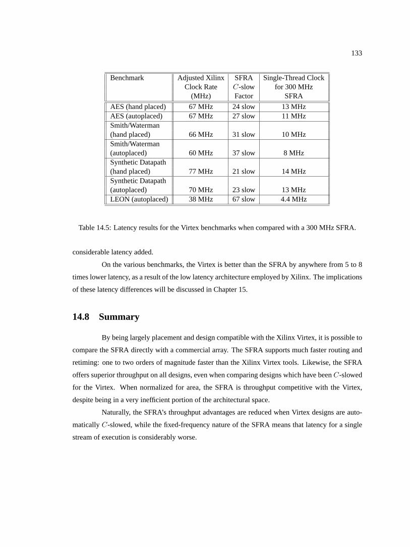
133
Benchmark Adjusted Xilinx SFRA Single-Thread ClockClock Rate C-slow for 300 MHz
(MHz) Factor SFRA
AES (hand placed) 67 MHz 24 slow 13 MHzAES (autoplaced) 67 MHz 27 slow 11 MHzSmith/Waterman(hand placed) 66 MHz 31 slow 10 MHzSmith/Waterman(autoplaced) 60 MHz 37 slow 8 MHzSynthetic Datapath(hand placed) 77 MHz 21 slow 14 MHzSynthetic Datapath(autoplaced) 70 MHz 23 slow 13 MHzLEON (autoplaced) 38 MHz 67 slow 4.4 MHz
Table 14.5: Latency results for the Virtex benchmarks when compared with a 300 MHz SFRA.
considerable latency added.
On the various benchmarks, the Virtex is better than the SFRA by anywhere from 5 to 8
times lower latency, as a result of the low latency architecture employed by Xilinx. The implications
of these latency differences will be discussed in Chapter 15.
14.8 Summary
By being largely placement and design compatible with the Xilinx Virtex, it is possible to
compare the SFRA directly with a commercial array. The SFRA supports much faster routing and
retiming: one to two orders of magnitude faster than the Xilinx Virtex tools. Likewise, the SFRA
offers superior throughput on all designs, even when comparing designs which have beenC-slowed
for the Virtex. When normalized for area, the SFRA is throughput competitive with the Virtex,
despite being in a very inefficient portion of the architectural space.
Naturally, the SFRA’s throughput advantages are reduced when Virtex designs are auto-
maticallyC-slowed, while the fixed-frequency nature of the SFRA means that latency for a single
stream of execution is considerably worse.
134
Chapter 15
Latency and Throughput: Is
Fixed-Frequency a Superior Approach?
“Never underestimate the bandwidth of a station wagon full of tapes hurling down the highway”
-Andrew S Tannenbaum
Fixed-frequency FPGAs, by virtue of a higher degree of pipelining, offer superiorthrough-
putover conventional FPGAs on a wide variety of tasks. Yet throughput alone is a misleading met-
ric, as any application that can benefit from a high degree of automatic repipelining orC-slowing
and retiming can also easily benefit from replication.
If an application is feed-forward, every datum is independent. Thus, it is possible to start
with a design for a single pipeline and simply replicate that pipeline to increase the throughput.
If an application can beC-slowed, there areC independent tasks. Thus, the initial design can be
replicatedC times instead of beingC-slowed. The application can also benefit from a compromise:
An initial core isC-slowed, and then replicated if even more throughput is desired.
By this observation, throughput is an insufficient metric for comparison, as it is half of an
efficiency metric, throughput/area or throughput/$ that needs to be considered. If greater throughput
is desired, more resources can be acquired to speed the computation. Eventually limits are reached,
but for most applications where fixed-frequency arrays are intended, the throughput limits are often
very high. Thus throughput/area represents a cost, not an intrinsic property, for implementations
that can benefit from aggressive repipelining,C-slowing, or replication.
Throughput’s scalability contrasts sharply withlatency, the time required to complete
the computation for a single element. Initially, the latency for a computation can be improved by

135
expending more resources, up to the point where resource limits no longer constrain the design’s
critical path. Beyond this point, adding more resources will not improve a design’s latency.
A good illustration of the relationship between throughput and latency appears in the
network world. Whenever more network bandwidth is required, it is usually possible to aggregate
links. Thus if a single T1 line, at 1.5 Mbps, has insufficient bandwidth, a second line can usually be
added for a linear increase in cost and complexity.
Yet network latency, the time it takes to transmit a single datum, is an intrinsic property
of the network’s implementation. Increasing the amount of resources employed generally cannot
improve network latency. In the ultimate limit, network latency is bounded by the speed of light, as
information can’t be sent any faster.
One of the highest bandwidth networks, described famously by Tannenbaum, involves
simply moving physical media from one location to another. Yet this technique is seldom employed,
as the latency is often unacceptably high despite the outstanding throughput and throughput/$.
The same tradeoffs apply to computational fabrics. Fixed-frequency FPGAs, that provide
high throughput through fine pipelining, increase the latency. The more aggressive the pipelining
involved, the greater the latency penalty. Additionally, a conventional FPGA could be treated as
nearly fixed-frequencythroughC-slowing tools when targeting throughput-limited designs, but a
fixed-frequency FPGA, unless there are architectural changes to bypass registers, can’t behave like
a conventional FPGA for latency bound tasks.
15.1 The Limits of Parallelism
The compiler community has long recognized the limits on parallelism. Anyloop-carried
dependency, a reference to a value computed in a previous iteration of the loop, acts to limit the
amount of parallel computation that can be performed. Even on an infinitely parallel machine, such
as a hypothetical infinite superscalar or VLIW architecture, the computational performance for the
loop will be limited by the time it takes to complete each loop iteration sequentially. In the extreme
case, where everything else can be computed in parallel, the latency of the loop’s iteration will
bound the maximum performance of the system.
Many important applications, including those that work well on FPGAs, include latency-
bound tasks. Cryptography, as discussed in Section 15.2, will often be latency bound. Other tasks,
such as Zero Length Encoding (ZLE) are also inherently sequential.

136
15.2 Latency and Cryptography
An effective illustration where computational latency is important arises from cryptogra-
phy. The NIST recommended modes of operation [51] for using block ciphers such as AES [50] are
ECB (Electronic Code Book), CBC (Cipher Block Chaining), CFB (Ciphertext Feedback Mode),
OFB (Output Feedback Mode), and CTR (Counter) modes. Of the five modes, CBC, CFB, and OFB
have inate feedback loops, requiring the complete encryption of one block before the next block can
be processed.
ECB and CTR modes attempt to provide security without creating inter-block feedback
loops, enabling these modes to be fully pipelined. Yet both these modes suffer significant limita-
tions. If an encrypted block is repeated when using ECB mode, the output will be repeated as well,
a serious limitation. Worse, both ECB and CTR mode provide no integrity or authentication. As a
result, these modes are very easy for implementers to misuse.
These limits on authentication and integrity enable an attacker who can replace encrypted
messages to distort communications. As an example, if an attacker knows that CTR mode is being
used, the decrypted block1 is the messageM , and the encrypted block isE, the attacker can sub-
stitute the messageM ′ by replacingE with E xor M xor M ′, because the firstxor will recover
the encrypted counter block and the secondxor will now be equivalent to counter-mode encrypting
M ′.2
The commonly-employed solution is to provide a separate integrity, or authentication
step, in the cryptographic pipeline to detect such manipulations. This is accomplished by either
cryptographically hashing the message and encrypting the result3 or using a message authentication
code (MAC) that is transmitted at the end of the message. Hashes are usually separate algorithms
that contain feedback loops, while MACs are based on block ciphers.
Although there is an explicitly parallel MAC, PMAC [13], most MACs, such as XCBC
MAC [12], RMAC [37] and the classic CBC MAC contain inter-block feedback. Because message
integrity and authentication is critical for real systems, if the hash or MAC requires a feedback
loop, it will be latency, not throughput, that limits the peak performance for encrypting a single
1This could be guessed. A good target would be default values (such as a shipping or billing address) that the attackerdesires to change.
2This attack works because CTR mode encrypts a counter value andxors the counter value with the messageM tocreate the encrypted blockE, enabling anyone who knows bothE andM to obtain the encrypted value of the counter.This is an intrinsic weakness ofall stream ciphers. While AES is a block cipher, CTR mode converts a block cipher intoa stream cipher.
3Note that this method can, when used with Counter mode, still enable an attacker to substitute a message if theattacker knows the entire message, the hash function, and any salting used.

137
communication channel.
Even in the case of PMAC, there is a final step that requires the completion of all previous
encryptions, before the final encryption is performed. For applications such as IPsec, each packet
needs its own authentication. Thus PMAC may still be latency-bound when small packets need to
be encrypted.
15.3 Latency and Fixed-Frequency FPGAs
Fixed-frequency arrays almost invariably add registers to the design to meet the array’s
intrinsic timing requirements. Although such registers, when added through repipelining orC-slow
retiming, do not degrade throughput,4 these registers will produce a serious impact on computational
latency.
The latency is added through three mechanisms: a greater number of setup and clk→Q
times, the irregular addition of additional pipelining, and extra registers before or after the critical
loop if C-slowing is employed. The setup and hold times impose a minimum added latency, while
the irregular pipelining represents the worst-case addition. TheC-slowing registers represent a tool
deficiency that may be addressable to a limited degree, although it would disrupt the cleanC-slow
semantics.
Consider a design where the latency is defined by a computational path withi registers that
is retimed and mapped to a variable frequency array as well as a fixed-frequency array. The design,
after remapping for the fixed-frequency array, now hasj registers on the computational path. Even
if the computational path is perfectly divided for the fixed-frequency FPGA, it now passes through
j− i additional registers. Thus the latency will be increased, at an absolute minimum, byj− i setup
and clk→Q times.
Additionally, if the division is not perfect, additional latency will be added to the design.
Every division whose computation and communication is less than the full array’s cycle-time rep-
resents wasted time that is added to the latency. These failures in division arise from architectural
restrictions, not just tool limitations. As an example, if the cycle-time for a fixed-frequency array
enables a signal to travel through four sections of interconnect before a register is required, a fifth
section of interconnect will always result in a significant latency penalty. Similarly, crossing only
three segments of interconnect may take as long as crossing four segments.
TheC-slowing penalty arises whenC registers are required to meet timing through one
4Indeed, these registers enable high throughput operation.

138
cycle of the computation, but the total graph of the computation now has more registers than are
strictly necessary to meet timing. A common case is when an inner loop isC-slowed, but the input
and output paths now also haveC-additional registers applied.
This could be corrected by smarter tools. However the resulting design will lose theC-
slow semantics and may have an awkward timing and interface model. ThusC-slowing, although
finding a solution that guarantees optimal throughput with the minimum number of additional exe-
cution streams, will not find a solution that minimizes latency for a single computation.
The net result is that a fixed-frequency FPGA will have substantially worse latency, when
compared with a conventional FPGA, an observation clearly demonstrated in Chapter 14. The more
aggressively pipelined the fixed-frequency array, the greater the penalty, as there are now even more
registers on the critical path.
15.4 Pseudo-Fixed-Frequency FPGA tools
If a fixed-frequency model is desired but the only FPGA available is a conventional array,
it is possible to modify aC-slowing tool to impose a pseudo-fixed-frequency constraint. In this
case, theC-slow tool would operate like a fixed-frequency tool: generate a set of local constraints
which will insure that any connection exceeding the delay are registered and then iterate to find the
minimumC which meets these constraints.
The constraint generation, however, does not involve just local constraints. It is necessary
to partially solve the shortest-paths problem from each source node to discover the frontier where all
signals will require registering. Thus although it is not the complete all-pairs-shortest-path problem,
the worst-case running time and memory usage is the same. All such links will then need to be
considered in the constraint-solving test, increasing the complexity of the constraint-solver as well.
However, with a conventional array, it may not be possible to meet a given timing con-
straints if too many flip-flops are allocated, as there is no longer an architectural guarantee that
every connection will be appropriately registered. Thus even when utilizing aC-slow tool, the pro-
cess may fail to meet the target clock, suggesting that if a conventional array is to be utilized in a
fixed-frequency mode, there will need to be fallback positions (such as time-multiplexed I/O logic
combined with replication of a slower core) to enable a slower internal clock rate while maintaining
an externally fixed interface.
139
15.5 Recommendations & Conclusions
If throughput/area or throughput/$ are the primary requirement a fixed-frequency FPGA’s
advantages outweigh the latency penalty. Traditionally, there have been numerous reconfigurable
arrays designed to perform only limited tasks. For example, feed-forward pipelines as targeted by
PipeRench [57], or pipelined datapaths as targeted by Garp [30], represent subclasses of the general
class of throughput-bound designs which benefit from aggressive pipelining orC-slow retiming.
If an array is designed for general computation, not just the tasks that benefit from high
throughput through fine pipelining, the latency limitations for a fixed-frequency design are substan-
tial. Worse, throughput deficiencies can be largely corrected by expending more resources (only
affecting various system costs), while latency limits are fundamental to the computational fabric
and can’t be corrected without changing the fabric itself. This is especially visible if there are a
family of computational devices of various sizes utilizing the same computational fabric.
This strongly suggests that any fixed-frequency FPGA that is targeted as a general compu-
tational fabric or coprocessor needs to be able to act like a conventional FPGA. Most or all registers
should be bypassable with the resulting array’s clock frequency determined by the mapped design
if low latency operation is desired. Likewise, interconnect should be constructed for low latency
operation when the registers are bypassed.
A compromise, where the array’s clock can be one of several different, prearranged fre-
quencies, will substantially help latency-bound tasks, but the difference between the optimum fre-
quency and the operating frequency may still hurt latency.
Such semi fixed-frequency arrays will still be comparatively area-inefficient, when com-
pared to conventional FPGAs, when the tasks are latency-bound. Due to the fully registered inter-
connect and similar restrictions, the basic logic tile will be substantially larger. As seen in Chap-
ter 13 and discussed earlier in this chapter, it is possible to aggressivelyC-slow conventional FPGA
designs to increase their throughput at a very minor area penalty. However, reducing the latency of
a fixed-frequency array by bypassing registers, does not reduce the area cost of the fixed-frequency
approach.
These observations suggest an alternate approach: a conventional array with several fixed
clock frequencies, using the modified tool techniques to impose a pseudo fixed-frequency constraint,
might serve the same purpose as a fixed-frequency FPGA when throughput is required but offer
superior performance on latency bound tasks.
Chapter 13 demonstrates thatC-slow retiming can substantially increase the throughput

140
of designs targeting a conventional FPGA. It would be only a minor modification to select a target
critical path and attempt to discover the minimumC required to meet the desired path, instead of
the tool’s model of finding the minimum critical path for a givenC.
Because there are several high quality, commercial FPGA designs available that are al-
ready optimized for low-latency operation and can achieve high throughput with better tools, in-
cluding being used in a pseudo-fixed-frequency manner, conventional FPGAs should be strongly
considered, even with the additional complications, when implementing reconfigurable coproces-
sors and related elements if latency is a concern.
141
Chapter 16
Open Questions
As it is impossible to cover all possible issues in a thesis, there are several issues that may
be considered for future work. There are three major unresolved issues involving the topics in this
thesis: the power implications ofC-slowing, the relative costs of corner-turn based coarse-grained
FPGAs, and proper strategies for depopulating the C-boxes while still maintaining fast-routing.
16.1 Power Consumption andC-slowing
Higher-throughput, achieved through high-speed clocking, naturally increases the power
consumption of a design, just as replicating units for higher throughput also increases power con-
sumption. In both cases, if lower power is desired, the higher throughput design can be modified to
save power by reducing the clock rate and operating voltage.
The common equation for dynamic power,P = CV 2F , suggests that lowering the fre-
quency linearly lowers the voltage and throughput. However, as first observed by Chandrakasan
et al [17], the lowering of the frequency also allows the voltage to be lowered, resulting in power
savings. This works quite effectively when replication is utilized, as replication doesn’t increase the
activity-factor of each node.
Unlike the replicated case, it is highly design and usage-dependent whether aC-slowed
design would offer power savings if both frequency and voltage were reduced. Although the finer
pipelining allows the frequency and the voltage to be scaled back to a significant degree while
maintaining throughput, the activity factor of each signal may now be considerably higher.
As each of theC streams of execution is completely independent, it is safe to assume
that every wire will now have an activity factor of 50%, as the separate streams will probably be
142
uncorrelated. Whether the initial design beforeC-slowing has a comparable activity factor is highly
input and design dependent.
If the original design’s activity factor is low then theC-slowed design will consume more
power even after lowering the frequency and voltage, as more signals will switch on each clock
cycle. While if the original design’s activity factor is already high than theC-slowed design will
result in substantial power savings, as the voltage can now be safely lowered while maintaining the
same level of throughput. Thus although theC-slowing transformation may have a minor affect on
worst-case power (and can even result in significant savings through voltage-scaling), the impact on
average-case power may be substantial.
As a concrete example, a block-cipher core, such as the AES core, will effectively have
a 50% activity factor on all lines even for a single stream of execution. Thus, aC-slowed design
won’t increase the activity factor, suggesting thatC-slowing may be appropriate for a low-power
cryptographic core.
Yet the Smith/Waterman core would experience dramatically increased power consump-
tion afterC-slowing. Because the inner loop involves repeatedly adding and subtracting 5 bit quan-
tities from a 16 bit register, the upper bits will experience a much lower activity factor. Thus, after
C-slowing, Smith/Waterman will utilize considerably more power per calculation as the activity
factor will be substantially increased.
A related question involves treating clock-gated circuits whenC-slowing. If the gated-
clock is converted to a clock-enable (and therefore converted into explicit logic), the semantics
should be properly maintained, although this will result in substantially increased power consump-
tion.
A potential alternative observes that many of these gated register-results don’t represent
clock-enabled registers but instead are “don’t-care” values, where the register contents simply won’t
matter. Such registers, instead of using a gated clock, could utilize a feedback loop to preserve the
last value. Although this violates theC-slow semantics, the result doesn’t matter due to the don’t-
care nature of the value will prevent the register and downstream nodes from changing in value.
Unfortunately, this doesn’t offer clock distribution savings, and it is unclear the total level of power
savings which would result.

143
16.2 Corner-Turn Interconnect and Coarse-Grained FPGAs
The corner-turn topology’s use of fully-populated C-boxes is considerably less efficient
for bit-oriented arrays when compared with word-oriented arrays. As an example, a corner-turn
interconnect designed for 8 bit words uses only1/8 the number of switches per wire and only1/8
of the configuration storage per wire.
Since the SFRA’s interconnect is switch dominated rather than wire dominated, reducing
the number of switches per wire reduces the cost of the interconnect while still maintaining the fast
routing, defect tolerance, and related properties.
Unfortunately, it is unknown (and currently unknowable) how much these interconnect
savings will change the relative costs if comparisons like those of Chapter 14 are desired. There
are no commercially successful coarse-grained FPGAs and the problem of efficiently mapping to a
coarser-grained structure remain unsolved, although there are considerable efforts, including Oskin
et al’s attempt to develop a sea-of-ALUs to map arbitrary C-code [69], as well as several startups
[16, 26].
If a successful sea-of-ALUs or similar coarse-grained FPGA was developed, it would then
be straightforward to estimate the cost of a corner-turn network by taking the layout components for
the SFRA, depopulating the switches to match the target’s wire schedule, and adapting the routing
tool to accept the target’s input format. But until such an array and accompanying toolflow is
created, it is impossible to perform reasonable comparisons.
16.3 Depopulated C-boxes
Another question is whether the C-boxes can be depopulated while still maintaining the
fast-routing properties. As the current C-boxes are switch dominated, depopulating theses C-boxes
should result in substantial area savings.
The key question is whether there exists a substantial depopulation where detailed rout-
ing can still occur independent of global routing. Global routing relies that all turns have identical
behavior, thus the selection of a particular turn at a particular switchpoint is irrelevant. Global
routing’s search techniques requires that turns be interchangeable, as without this requirement, the
search would not be choosing between equal-cost paths. Without this property, the individual chan-
nels would not be independent and global routing could not be separated from detailed routing.
Likewise, even if all turns are identical, it is an open question whether there exist fast-
144
heuristics to perform detailed routing within these depopulated channels. Although conventional
FPGA routing algorithms could be employed, these heuristics lack the speed and comprehensive
nature of channel independent packing which guarentee a fixed routing overhead andO(n lg n)
runtime. Naturally, most depopulations would prevent the defect tolerance technique described in
Chapter 9 from being applied.
16.4 Summary
This section developed the major open questions arising from this thesis. The power-
effects caused byC-slowing are generally unknown and highly design dependent. Comparing the
relative costs of a corner-turning, coarse-grained array when compared with a conventional coarse-
grained array are limited by the difficulty in mapping designs to such arrays. Finally, depopulated
C-boxes will complicate routing, and it is an open question if a suitable depopulation can maintain
fast global and detailed routing while saving area.
145
Chapter 17
Conclusion
The first part of this thesis presented a new FPGA interconnect topology, a “corner-turn”
interconnect, and used this to develop the SFRA FPGA architecture. Unlike other FPGA topologies,
the corner-turn topology supports fast routing, pipelined interconnect, and a degree of fine grained
defect tolerance, while maintaining conventional Manhattan placement properties. Routing for a
corner-turn array uses fast, polynomial time heuristics. A 6000 LUT design can be routed in 11
second, vastly faster than the 7 minutes to needed to route the same design when targeting a Xilinx
Virtex.
The SFRA is a fixed-frequency FPGA, using the corner-turn interconnect, which is largely
placement and design comparable with the Xilinx Virtex FPGA. Thus the same design can be
mapped to both a Virtex and the SFRA to facilitate high-quality comparisons. Simultaneously,
the SFRA can utilize existing synthesis and placement tools.
The second part of this thesis extended the understanding ofC-slow retiming. This pow-
erful transformation can be applied whenever there is available task-level parallelism. One signifi-
cant application is applying this transformation to a microprocessor core, automatically producing
a multithreaded architecture. Each thread will operate at a lower clock frequency, but the aggre-
gate design’s throughput will be substantially improved through the action of multiple threads. An
automaticC-slow retiming tool was developed for designs targeting the Xilinx Virtex, effectively
doubling the throughput on the benchmark designs.
Since the SFRA is fixed-frequency, it requires theC-slowing tool to automatically remaps
all designs so they operate at the SFRA’s clock. Not only does this guarantee the clock-rate for all
successfully mapped designs, but retiming for a fixed-frequency architecture like the SFRA runs
substantially faster than retiming for a conventional FPGA like the Virtex.
146
The resulting designs, when targeted for the SFRA, run substantially faster. As an ex-
ample, the AES core whenC-slowed and mapped to the Xilinx would run at approximately 150
MHz, but would operate at 300 MHz in a comparable SFRA. Even when normalized for area, the
SFRA is reasonably competitive with the Virtex, given that the corner-turn architecture is better
targeted at coarse-grained FPGAs while the Virtex is a 5th generation commercial product, with an
interconnect topology highly optimized for bit-oriented tasks.
In the following sections, there are four areas of this thesis which are reviewed in more
detail. The first is benchmark selection, as the choice of benchmarks greatly aided this research.
The second is the SFRA architecture and the implications discovered in its design. The third area is
the effects ofC-slowing, which is applicable to a wide variety of designs. The final section involves
how this research might benefit commercial products.
17.1 Benchmark Selection
Evaluations are often limited by the quality of the benchmarks. Although having more
benchmarks would have offered more datapoints, an early decision was made to focus on a few,
high-quality benchmarks (Chapter 3 and Appendix A). Most of the existing FPGA benchmarks
are either the proprietary property of the FPGA companies (who assemble their own application-
based suites), microbenchmarks such as the MCNC suite, or functional benchmarks which require
reimplementation for various targets.
The three benchmarks created specifically for this thesis proved to be remarkably flexible
evaluation tools. By including both hand and automatic placement, these benchmarks could be used
to gauge the quality of the Xilinx placement tool (Chapter 12) and to isolate the effects of placement
when comparing the Virtex with the SFRA (Chapter 14). Likewise, the handC-slowing allowed an
evaluation of the automaticC-slowing tool (Chapter 13).
Since the same benchmarks were used for both theC-slowing tool and the SFRA evalua-
tion, the SFRA was compared with the Xilinx both before and after the benefits ofC-slowing were
included (Chapter 14). Although including theC-slowed results for the Virtex make the SFRA seem
less favorable in comparison, this allowed the final results to separate the benefits ofC-slowing from
the benefits of a fixed-frequency interconnect, which leads to the conclusion that it is generally su-
perior to use a general FPGA with better tools, rather than a fixed-frequency array (Chapter 15).
Finding publicly available, application-based designs which use hand placement, let alone
handC-slowing, are nearly impossible. Although such designs are constructed on a regular basis

147
by professional designers,1 these designs are invariably proprietary.
Thus although creating benchmarks specifically for this thesis involved considerable ef-
fort (and therefore limited the number of benchmarks), these benchmarks proved extremely useful.
These custom benchmarks enabled studies which would not be possible with synthesized bench-
marks or microbenchmarks, as those benchmarks would require substantial reengineering.
17.2 The SFRA
The SFRA introduced two substantially new concepts: the corner-turn interconnect and
a fixed-frequency architecture which maintains Manhattan placement. Unlike previous academic
FPGAs, the SFRA is compatible with a successful, commercial FPGA, which enables direct com-
parisons.2
17.2.1 Corner Turn Interconnect and Fast Routing
The corner-turn interconnect structure offered several benefits, including Manhattan place-
ment, fast routing, and the ability to efficiently pipeline switchpoints. It is the Manhattan placement
and fast routing, not pipelined switchpoints, which offer the greatest benefits.
Since the corner-turn array maintains Manhattan placement, it can be used as a replace-
ment topology for large classes of FPGAs. This is especially appropriate for coarser-grained FP-
GAs, where the relative cost of corner-turn switches is reduced (Chapter 9).
The fast-routing advantage, an order of magnitude faster than a conventional FPGA (Chap-
ters 8 and 14), is a substantial improvement. Current FPGA routing algorithms take minutes to
complete, making them unsuitable for runtime design generation.
17.2.2 Compatibility
Unlike previous fixed-frequency arrays and other academic designs, the SFRA is largely
design and toolflow compatible with a modern FPGA, the Xilinx Virtex. The design-decision to
make the SFRA compatible with the Virtex proved to be an excellent aid in the research, as direct
1As just one example, Andraka Consulting Group’s (www.andraka.com) primary business is focused on creatinghand-placed, finely-pipelined designs.
2There have been a few academic arrays which are compatible with the Xilinx 6200, but that array was never com-mercially successful, and the 6200’s interconnect is both very restricted and very poor compared to a modern FPGAdesign.
148
compatibility offered two huge advantages by creating a complete toolflow and allowing direct
comparisons.
Having a compatible toolflow enabled better benchmarks: rather than small minibench-
marks like the MCNC suite, this thesis used 4 application-based benchmarks, all of which represent
important tasks for modern FPGAs. Being able to map a fully synthesized benchmark (LEON)
helped to established that the SFRA is truly a generic fixed-frequency array.
Likewise, compatibility also ensured that the upstream tools were of high quality. It takes
considerable effort to develop a high quality synthesis, packing, and placement tool. Although
commercial tools have their limitations (as evaluated in Chapter 12), market competition generally
ensures a reasonable quality of results. Thus by insuring compatibility, these high quality tools
could be used. And by including both hand and automatically placed versions of the three hand-
benchmarks, any artifacts which might have been introduced can be isolated.
By being directly compatible, the SFRA was also directly comparable to the Virtex (Chap-
ter 14). Most new FPGA architectures have to rely purely on internal comparisons, benchmarking
the FPGA against internal variants. The SFRA is different because it was compared with an existing
commercial product.
The SFRA router runs an order of magnitude faster (routing the 6000 LUT LEON core
in 11 seconds, when compared with several minutes for the Xilinx router), while retiming also runs
an order of magnitude faster. The SFRA, when the comparable Virtex designs are not automatically
C-slowed, offers better throughput per area. When the Virtex designs wereC-slowed, the Virtex
proved marginally superior, suggesting that a pseudo-fixed-frequency approach might be superior,
as it provides both improved throughput, easier interfacing, and better latency (Chapter 15).
Without the ability to conduct apples-to-apples comparisons, the benefits and costs of the
SFRA could not have been accurately estimated. This suggests that future academic FPGA designs
would also benefit from being as compatible as possible, as it allows a much better evaluation of the
costs and benefits associated with a new design.
17.2.3 Fixed Frequency Operation
Although the SFRA demonstrates that a fixed-frequency FPGA can be made design and
toolflow compatible with conventional architectures, that frequency guarantees can be maintained
on arbitrary designs, and can be throughput/area competitive with a commercial FPGA, this thesis
also demonstrated that fixed-frequency operation is of fairly limited overall benefit.
149
TheC-slowing and retiming tool (Chapter 13), although taking longer to complete when
targeting the Xilinx Virtex, offers substantial improvements in throughput. Without the automatic
C-slowing, the Virtex is significantly worse in throughput/area, but becomes competitive when this
or a similar tool is employed.
Yet a fixed-frequency architecture like the SFRA is substantially worse than a conven-
tional FPGA when latency is a concern (Chapter 15). As latency represents an intrinsic property of
the design and FPGA architecture, while throughput represents only a cost, it is probably better to
optimize the array for low latency and then rely on automatic tools to achieve a target throughput in
a pseudo-fixed-frequency manner, although pseudo-fixed-frequency does not provide a guaranteed
clock rate for all designs.
17.3 C-slowing and Retiming
Retiming andC-slowing are critical transformations for VLSI and FPGA CAD, able to
substantially increase throughput at a very low cost in area and complexity.
Although always known as a powerful transformation, the observation that aC-slowed
microprocessor is not only possible, but provides already understood multithreaded semantics, is
both novel and useful (Chapter 11). This can be used in both hand-implemented and automatically-
synthesized cores to create higher throughput, multithreaded designs.
Multithreading in this manner offers the most benefits forin-order designs, in sharp con-
trast to SMT which applies to out-of-order architectures. Thus interleaved-multithreading through
C-slowing can be effectively applied to large classes of in-order architectures, including vector pro-
cessors and in-order superscalar designs. It is probably worth evaluating a hypothetical two-thread,
narrow issue (3 instruction/cycle) IA64 to see what the costs and benefits are when this technique is
applied to a complex, conventional architecture.
AutomaticC-slowing offers substantial benefits (Chapter 13). All benchmarks showed
significant increases in throughput at a relatively minor cost in additional registers. In practice,
these additional registers only cost power, not area, as the tool is using unutilized registers in the
FPGA to enableC-slowing. The throughput benefits are substantial, doubling the throughput on the
synthesized LEON benchmark, and nearly doubling the throughput on all tested benchmarks.
The retiming transformation is much faster when applied to a fixed-frequency architec-
ture. This suggests that if retiming for a conventional FPGA could be approximated with local-
delays, without creating the global delay matrixes and global constraints, this should result in sub-
150
stantially improved performance with only a minor loss in precision.
17.4 Applications to Commercial Products
Three significant contributions of this thesis, automaticC-slow retiming, the effects of
C-slowing a microprocessor, and the corner-turn topology, offer substantial benefits for future com-
mercial products.
Several existing FPGA synthesis tools include retiming, but all lack the ability toC-
slow designs. Two changes to conventional synthesis tools would greatly increase their ability to
automatically improve designs.
The first addition would be aC-slow directive which could be added to the HDL source.
When applied to a block of code, theC-slow directive replaces every register withC registers in
series, increases all inferred memories by a factor ofC, and adds a thread-counter to all memo-
ries to enforce isolation. This would allow individual blocks to beC-slowed (and even recursively
C-slowed down in the hierarchy), while presenting a straightforward interface (cycle-by-cycle in-
terleaving of execution) to the external logic.
The second change would be a compiler or HDL flag which would disable initial con-
ditions. If the designer uses explicit startup logic on the state machines, then there is no need to
preserve initial conditions or global set/reset properties. This substantially increases the quality of
the resultingC-slowed design, while imposing only a minor penalty on the designer. By combining
both changes, conventional synthesis tools could provide benefits which are comparable or even
superior to those shown by the automaticC-slowing tool created for this thesis (Chapter 13).
C-slowing a microprocessor represents a new variant on multithreaded architectures. Al-
though interleaved-multithreading has been previously proposed,C-slowing not only increases the
memory-access efficiency, but also increases the clock rate through additional pipeliningwithout
increasing the complexity of the control and bypassing logic.
Since it can be applied to effectively arbitrary in-order cores, and can even be assisted
by automatic tools,C-slowing should offer a substantial throughput benefit to a wide range of
future processors, including embedded cores, in-order VLIW DSPs, network processors, and vector
microprocessors.
Finally, the corner-turn array, although actually inefficient when constructing a bit-oriented
array like the SFRA, is far more efficient when targeting a coarse grained (8, 16, 32, or 64 bit word)
reconfigurable architecture. Since the significant penalty for a corner-turn interconnect (the fully

151
populated C-boxes) is reduced by a coarse-grained architecture, while the benefits (including defect
tolerance, fast routing, heterogeneous channels, and possibly pipelined switchpoints) remain, this
interconnect seems very well suited to future coarse-grained reconfigurable devices.

152
Bibliography
[1] Altera Inc., 101 Innovation Drive, San Jose, CA 95134.ARM-Based Embedded Processor
Device Overview, 2000.
[2] Altera Inc., 101 Innovation Drive, San Jose, CA 95134.Apex II Programmable Logic Device
Family Data Sheet, 2002.
[3] Altera Inc., 101 Innovation Drive, San Jose, CA 95134.The Nios Embedded Processor, http:/
/www.altera.com/products/devices/nios/overview/nio-overview.html, 2002.
[4] Altera Inc., 101 Innovation Drive, San Jose, CA 95134.Stratix FPGA Family Data Sheet,
2002.
[5] Altera Inc., 101 Innovation Drive, San Jose, CA 95134.Stratix GX FPGA Family Data Sheet,
2002.
[6] Robert Alverson, David Callahan, Daniel Cummings, Brian Koblenz, Allan Porterfield, and
Burton Smith. The Tera computer system. InProceedings of the1990 International Conference
on Supercomputing, pages 1–6, 1990.
[7] Amphion Semiconductor.CS5210-40: High Performance AES Encryption Cores, 2001. http:/
/www.amphion.com/cs5210.html.
[8] Ray Andraka. Public comments in comp.arch.fpga.
[9] Peter Bellows and Brad Hutchings. JHDL – an HDL for reconfigurable systems. In Kenneth L.
Pocek and Jeffrey Arnold, editors,IEEE Symposium on FPGAs for Custom Computing Ma-
chines, Los Alamitos, CA, April 1998. IEEE Computer Society Press.
153
[10] Vaughn Betz and Jonathan Rose. Directional bias and non-uniformity in fpga routing architec-
tures. InProceeding of the IEEE/ACM International Conference on Computer-Aided Design,
pages 652–659, 1996.
[11] Vaugn Betz and Jonathan Rose. Vpr: A new packing, placement, and routing tool for fpga
research. InSeventh International Workshop on Field-Programmable Logic and Applications,
1997.
[12] John Black and Phillip Rogaway. A suggestion for handling arbitrary-length messages
with the cbc mac, http://csrc.nist.gov/cryptotoolkit/modes/proposedmodes/xcbc-mac/xcbc-
mac-spec.pdf.
[13] John Black and Phillip Rogaway. A block-cipher mode of operation for parallelizable message
authentication. InTheory and Application of Cryptographic Techniques, pages 384–397, 2002.
[14] Duncan A Buell, Jeffrey M Arnold, and Walter J Kleinfelder.Splash 2: FPGAs in a Custom
Computing Machine. IEEE Computer Society, 1996.
[15] Timothy Callahan. Automatic Compilation of C for Hybrid Reconfigurable Architectures.
PhD thesis, University of California, Berkeley, 2002. http://brass.cs.berkeley.edu/ timothyc/
callahanphd.pdf.
[16] Chameleon systems reconfigurable communication platform.
[17] Anantha Chandrakasan, Samuel Sheng, and Robert Brodersen. Low-power cmos digital de-
sign, 1992.
[18] Pawel Chodowiec, Po Khuon, and Kris Gaj. Fast implementations of secret key block cyphers
using mixed inner- and outer-round pipelining. InProceedings of the International Symposium
on Field Programmable Gate Arrays, February 2001.
[19] Michael Chu, Nicholas Weaver, Kolja Sulimma, Andre DeHon, and John Wawrzynek. Object
oriented circuit-generators in Java. In Kenneth L. Pocek and Jeffrey Arnold, editors,IEEE
Symposium on FPGAs for Custom Computing Machines, pages 158–166, Los Alamitos, CA,
April 1998. IEEE Computer Society Press.
[20] Jason Cong and Chang Wu. Optimal FPGA mapping and retiming with efficient initial state
computation. InDesign Automation Conference, pages 330–335, 1998.
154
[21] Andr‘e DeHon. Rent’s rule based switching requirements (extended abstract).
[22] Andre DeHon. Reconfigurable Architectures for General Purpose Computing. PhD thesis,
MIT, 1996.
[23] E. M. Sentovich, K. J. Singh, L. Lavagno, C. Moon, R. Murgai, A. Saldanha, H. Savoj, P. R.
Stephan, R. K. Brayton and A. Sangiovanni-Vincentelli. SIS: A system for sequential circuit
synthesis. Technical report, UC Berkeley, 1992.
[24] Carl Ebeling, Darren C Cronquist, and Paul Franklin. Rapid - reconfigurable pipelined dat-
apath. InThe 6th International Workshop on Field Programmable logic and Applications,
1996.
[25] AJ Elbirt, W Yip, B Chetwynd, and C Parr. An fpga implementation and performance eval-
uation of the aes block cypher candidate algorithm finalists. InProceedings of the Third
Advanced Encryption Standard Candidate Conference, pages 13–27, April 2000.
[26] Elixent d-fabrix reconfigurable algorithm processing, http://www.elixent.com.
[27] Christopher W. Fraser. A language for writing code generators. InProceedings of the SIG-
PLAN ’89 Conference on Programming language design and implementation, pages 238–245.
ACM Press, 1989.
[28] Kris Gaj and Pawel Chodowiec. Comparison of the hardware performance of the aes can-
didates using reconfigurable hardware. InProceedings of the Third Advanced Encryption
Standard Candidate Conference, pages 40–54, April 2000.
[29] Peter Hallschmid and Steven J. E. Wilton. Detailed routing architectures for embedded pro-
grammable logic ip cores. InNinth international symposium on Field programmable gate
arrays, pages 69–74. ACM Press, 2001.
[30] John R. Hauser and John Wawrzynek. Garp: A mips processor with a reconfigurable coproces-
sor. InProceedings of the IEEE Symposium on Field-Programmable Gate Arrays for Custom
Computing Machines, pages 12–21. IEEE, April 1997.
[31] John Reid Hauser.Augmenting a Microprocessor with Reconfigurable Hardware. PhD
thesis, University of California, Berkeley, 2000. http://www.jhauser.us/publications/
AugmentingProcWithReconfigHardware.html.

155
[32] Helion Technologies. High Performance AES (Rijndael) cores, 2001. http://
www.heliontech.com/core2.htm.
[33] Randy Huang, John Wawrzynek, and Andre DeHon. Stochastic, spatial routing for hyper-
graphs, trees, and meshes. InProceedings of the 2003 ACM/SIGDA eleventh international
symposium on Field programmable gate arrays, pages 78–87. ACM Press, 2003.
[34] Michael Hutton, Vinson Chan, Peter Kazarian, Victor Maruri, Tony Ngai, Jim Park, Rakesh
Patel, Bruce Pedersen, Jay Schleicher, and Sergey Shumarayev. Interconnect enhancements for
a high-speed pld architecture. InTenth ACM International Symposium on Field-Programmable
Gate Arrays, pages 3–10. ACM Press, 2002.
[35] Intel. Intel ixp1200 network processor, http://www.intel.com/design/network/products/
npfamily/ixp1200.htm.
[36] Intel. Intel hyper-threading technology, 2001. http://developer.intel.com/technology/
hyperthread/.
[37] E. Jaulmes, A. Joux, and F. Valette. the security of randomized cbc-mac beyond the birthday
paradox limit – a new construction, 2002.
[38] Andreas Koch. Structured design implementation: a strategy for implementing regular data-
paths on fpgas. InProceedings of the 1996 ACM fourth international symposium on Field-
programmable gate arrays, pages 151–157. ACM Press, 1996.
[39] B. S. Landman and R. L. Russo. On pin versus block relationship for partitions of logic
circuits. InIEEE Transactions on Computers, 1971.
[40] James Laudon, Anoop Gupta, and Mark Horowitz. Interleaving: A multithreading technique
targeting multiprocessors and workstations. InProceedings of the6th International Conference
on Architectural Support for Programming Languages and Operating Systems, pages 308–
318, 1994.
[41] Charles Leiserson, Flavio Rose, and James Saxe. Optimizing synchronous circuitry by retim-
ing. In Third Caltech Conference On VLSI, March 1993.
[42] Guy Lemieux, Paul Leventis, and David Lewis. Generating highly-routable sparse crossbars
for plds. InProceedings of the International Symposium on Field Programmable Gate Arrays,
pages 155–164, February 2000.
156
[43] Guy Lemieux and David Lewis. Using sparse crossbars within lut. InNinth international
symposium on Field programmable gate arrays, pages 59–68. ACM Press, 2001.
[44] David Lewis, Vaughn Betz, David Jefferson, Andy Lee, Chris Lane, Paul Leventis, Sandy Mar-
quardt, Cameron McClintock, Bruce Pedersen, Giles Powell, Srinivas Reddy, Chris Wysocki,
Richard Cliff, and Jonathan Rose. The stratix. routing and logic architecture. InProceedings
of the international symposium on Field programmable gate arrays, pages 12–20. ACM Press,
2003.
[45] Helger Lipmaa. Aes candidates: A survey of implementations, of implementations. constantly
updated on-line table, available from http://www.tml.hut.fi/helger/aes.
[46] Andrea Lodi, Mario Toma, and Fabio Campi. A pipelined configurable gate array for embed-
ded processors. InProceedings of the international symposium on Field programmable gate
arrays, pages 21–30. ACM Press, 2003.
[47] Larry McMurchie and Carl Ebeling. Pathfinder: A negotiation-based performance-driven
router for FPGAs. InFPGA, pages 111–117, 1995.
[48] Oskar Mencer, Martin Morf, and Michael J. Flynn. PAM-Blox: High performance FPGA
design for adaptive computing. In Kenneth L. Pocek and Jeffrey Arnold, editors,IEEE Sym-
posium on FPGAs for Custom Computing Machines, pages 167–174, Los Alamitos, CA, 1998.
IEEE Computer Society Press.
[49] E. Mirsky and A. DeHon. MATRIX: A reconfigurable computing architecture with config-
urable instruction distribution and deployable resources. In Kenneth L. Pocek and Jeffrey
Arnold, editors,IEEE Symposium on FPGAs for Custom Computing Machines, pages 157–
166, Los Alamitos, CA, 1996. IEEE Computer Society Press.
[50] NIST. Federal information processing standards publication 197: Advanced encryption stan-
dard, 2001. http://csrc.nist.gov/publications/fips/fips197/fips-197.pdf.
[51] NIST. Recommendations for block cypher modes of operation, nist special publication 800-
38a, 2001. http://csrc.nist.gov/publications/nistpubs/800-38a/sp800-38a.pdf.
[52] Emil S. Ochotta, Patrick J. Crotty, Charles R. Erickson, Chih-Tsung Huang, Rajeev Jayara-
man, Richard C. Li, Joseph D. Linoff, Luan Ngo, Hy V. Nguyen, Kerry M. Pierce, Douglas P.

157
Wieland, Jennifer Zhuang, and Scott S. Nance. A novel predictable segmented fpga routing
architecture. InProceedings of the 1998 ACM/SIGDA sixth international symposium on Field
programmable gate arrays, pages 3–11. ACM Press, 1998.
[53] Paracel genematcher2, http://www.paracel.com/products/genematcher2.php.
[54] Gaisler Research. The LEON SPARC Processor, http://www.gaisler.com/leonmain.html.
[55] Raphael Rubin and Andr’e DeHon. Design of fpga interconnect for multilevel metalization.
In Proceedings of the international symposium on Field programmable gate arrays, pages
154–163. ACM Press, 2003.
[56] Atri Rudra, Pradeep Dubey, Charanjit Jutla, Vijay Kumar, Josyula R Rao, and Pankaj Rohatgi.
Efficent rijndael encryption implementation with composite field arithmetic. InProceedings
of the Chryptographic Hardware in Embedded Systems (CHES) Workshop, pages 171–184,
2001.
[57] Herman Schmit. Incremental reconfiguration for pipelined applications. InProceedings of
the IEEE Symposium on Field-Programmable Gate Arrays for Custom Computing Machines,
pages 47–55. IEEE, April 1997.
[58] Herman Schmit and Vikas Chandra. Fpga switch block layout and evaluation. InTenth ACM
International Symposium on Field-Programmable Gate Arrays, pages 11–18. ACM Press,
2002.
[59] Bruce Schneier, John Kelsey, Doug Whiting, David Wagner, Chris Hall, and Niels Ferguson.
Twofish: A 128-bit block cypher. Inhttp://www.counterpane.com/twofish.html, 1998.
[60] Akshay Sharma, Carl Ebeling, and Scott Hauck. Piperoute: a pipelining-aware router for
fpgas. InProceedings of the international symposium on Field programmable gate arrays,
pages 68–77. ACM Press, 2003.
[61] Amit Singh, Arindam Mukherjee, and Malgorzata Marek-Sadowska. Interconnect pipelin-
ing in a throughput-intensive fpga architecture. InNinth international symposium on Field
programmable gate arrays, pages 153–160. ACM Press, 2001.
[62] Deshanand P. Singh and Stephen D. Brown. The case for registered routing switches in field
programmable gate arrays. InNinth international symposium on Field programmable gate
arrays, pages 161–169. ACM Press, 2001.
158
[63] Deshanand P. Singh and Stephen D. Brown. Integrated retiming and placement for field pro-
grammable gate arrays. InTenth ACM International Symposium on Field-Programmable Gate
Arrays, pages 67–76. ACM Press, 2002.
[64] S. Singh and P. James-Roxby. Lava and jbits: From hdl to bitstreams in seconds, 2001.
[65] Satnam Singh. Death of the rloc? InProceedings of the 2000 IEEE Symposium on Field
Programmable Custom Computing Machines, pages 155–164, February 2000.
[66] Burton J Smith. Architecture and applications of the HEP multiprocessor computer system.
[67] Temple Smith and Michael Waterman. Identification of common molecular subsequences.
Journal of Molecular Biology, 147:195–197, 1981.
[68] SPARC International, Inc. http://www.sparc.org.
[69] Steven Swanson, Ken Michelson, and Mark Oskin. Wavescalar, http://
www.cs.washington.edu/homes/oskin/wavescalar.pdf.
[70] Amplify, http://www.synplicity.com/products/amplify/.
[71] Synplify pro, http://www.synplicity.com/products/synplifypro/index.html.
[72] Synopsys Inc.Synopsys FPGA Compiler II.
[73] Decypher bioinformatics accelerator, http://www.timelogic.com/decypherintro.html.
[74] William Tsu, Kip Macy, Atul Joshi, Randy Huang, Norman Walker, Tony Tung, Omid
Rowhani, Varghese George, John Wawrzynek, and Andre DeHon. HSRA: High-speed, hi-
erarchical synchronous reconfigurable array. InProceedings of the International Symposium
on Field Programmable Gate Arrays, pages 125–134, February 1999.
[75] Dean Tullsen, Susan Eggers, and Henry Levy. Simultaneous multithreading: Maximizing on-
chip parallelism. InProceedings of the 22rd Annual International Symposium on Compute r
Architecture, pages 392–403, June 1995.
[76] US Department of Commerce/National Institute of Standards and Technology. Federal in-
formation processing standards publication 46-3, data encryption standard (DES), http://
csrc.nist.gov/publications/fips/fips46-3/fips46-3.pdf, 1999.

159
[77] S. Wolter, H. Matz, A. Schubert, and R. Laur. The vlsi implementation of the international
data encryption algorithm idea. Proceedings of the IEEE International Symposium on Circuits
and Systems, vol. 1, pp. 397–400, 1995.
[78] Xilinx system generator for dsp, http://www.xilinx.com/xlnx/
xil prodcatproduct.jsp?title=systemgenerator.
[79] Xilinx, Inc. JBits SDK, http://www.xilinx.com/products/jbits/.
[80] Xilinx, Inc. Xilinx CORE Generation System, http://www.xilinx.com/products/logicore/
coregen/.
[81] Xilinx, Inc., 2100 Logic Drive, San Jose, CA 95124.Xilinx 6200 Field Programmable Gate
Arrays, 1996.
[82] Xilinx, Inc., 2100 Logic Drive, San Jose, CA 95124.Virtex Series FPGAs, 1999.
[83] Xilinx, Inc., 2100 Logic Drive, San Jose, CA 95124.Virtex 2 Series FPGAs, 2001.
[84] Xilinx, Inc., 2100 Logic Drive, San Jose, CA 95124.Virtex 2 Pro Series FPGAs, 2002.
[85] Xilinx, Inc., 2100 Logic Drive, San Jose, CA 95124.Spartan 3 1.2V FPGA Family, 2003.
[86] Xilinx, Inc., 2100 Logic Drive, San Jose, CA 95124.Xilinx Microblize Soft Processor, http://
www.xilinx.com/xlnx/xilprodcatproduct.jsp?title=microblaze, 2003.
160
Appendix A
Case Study: AES Encryption
Many current high performance FPGA designs often require considerable effort, with
hand placement and careful pipelining needed to achieve high throughput. One of the primary goals
of a fixed-frequency array is to reduce this pressure: any design which is throughput bound and
which can be mapped to the target fabric will operate at the desired clock rate. Likewise, automatic
tools for conventional arrays which can repipeline designs for higher performance also ease pressure
on the designer.
This appentix presents a typical high performance design using current tools targeting
commercial FPGAs, able to operate at 115 MHz on a<$10 commercial FPGA. It clearly demon-
strates the design techniques needed to achieve high performance on conventional FPGAs. Since
a fixed-frequency FPGA can automate and ease the process of producing high throughput designs,
understanding the effort required for conventional high-performance design provides excellent mo-
tivation for the remaining work in this thesis.
This design also provides an illustration of how throughput and latency are often different
goals: a throughput oriented design may offer superior throughput, but the latency for an individual
calculation is significantly worse. Likewise, throughput can be easily scaled, but latency can’t
be improved by adding more resources. These themes on latency and throughput are discussed
Chapter 15, as these tradeoffs directly reflect on the suitability of fixed-frequency FPGAs.
This design represents one of the three hand-constructed benchmarks in Chapter 3 used
throughout this thesis. The techniques used to implement this benchmark: careful placement and
handC-slowing are also employed on the other two hand-implemented benchmarks.
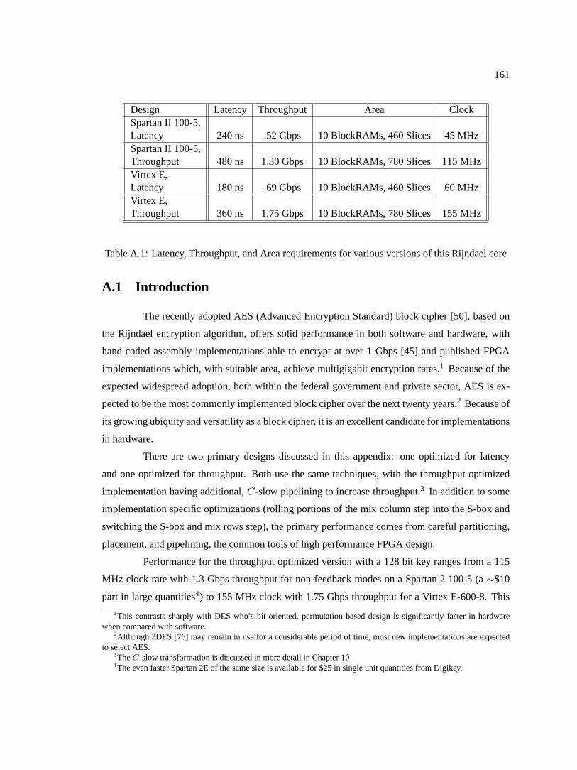
161
Design Latency Throughput Area ClockSpartan II 100-5,Latency 240 ns .52 Gbps 10 BlockRAMs, 460 Slices 45 MHzSpartan II 100-5,Throughput 480 ns 1.30 Gbps 10 BlockRAMs, 780 Slices 115 MHzVirtex E,Latency 180 ns .69 Gbps 10 BlockRAMs, 460 Slices 60 MHzVirtex E,Throughput 360 ns 1.75 Gbps 10 BlockRAMs, 780 Slices 155 MHz
Table A.1: Latency, Throughput, and Area requirements for various versions of this Rijndael core
A.1 Introduction
The recently adopted AES (Advanced Encryption Standard) block cipher [50], based on
the Rijndael encryption algorithm, offers solid performance in both software and hardware, with
hand-coded assembly implementations able to encrypt at over 1 Gbps [45] and published FPGA
implementations which, with suitable area, achieve multigigabit encryption rates.1 Because of the
expected widespread adoption, both within the federal government and private sector, AES is ex-
pected to be the most commonly implemented block cipher over the next twenty years.2 Because of
its growing ubiquity and versatility as a block cipher, it is an excellent candidate for implementations
in hardware.
There are two primary designs discussed in this appendix: one optimized for latency
and one optimized for throughput. Both use the same techniques, with the throughput optimized
implementation having additional,C-slow pipelining to increase throughput.3 In addition to some
implementation specific optimizations (rolling portions of the mix column step into the S-box and
switching the S-box and mix rows step), the primary performance comes from careful partitioning,
placement, and pipelining, the common tools of high performance FPGA design.
Performance for the throughput optimized version with a 128 bit key ranges from a 115
MHz clock rate with 1.3 Gbps throughput for non-feedback modes on a Spartan 2 100-5 (a∼$10
part in large quantities4) to 155 MHz clock with 1.75 Gbps throughput for a Virtex E-600-8. This
1This contrasts sharply with DES who’s bit-oriented, permutation based design is significantly faster in hardwarewhen compared with software.
2Although 3DES [76] may remain in use for a considerable period of time, most new implementations are expectedto select AES.
3TheC-slow transformation is discussed in more detail in Chapter 104The even faster Spartan 2E of the same size is available for $25 in single unit quantities from Digikey.
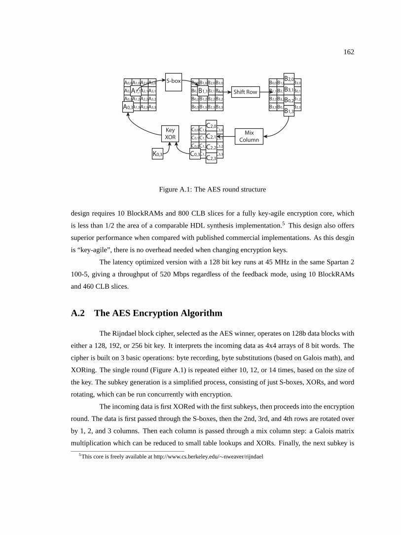
162
A0,3
A0,2
A0,1
A0,0
A1,3
A1,2
A1,1
A1,0
A2,3
A2,2
A2,1
A2,0
A3,3
A3,2
A3,1
A3,0 S-box
A1,1
B0,3
B0,2
B0,1
B0,0
B1,3
B1,2
A1,1
B1,0
B2,3
B2,2
B2,1
B2,0
B3,3
B3,2
B3,1
B3,0
B1,1
B3,3
B2,2
B1,1
B0,0
B0,3
B3,2
B2,1
B1,0
B1,3
B0,2
B3,1
B2,0
B2,3
B1,2
B0,1
B3,0
Shift Row
B2,0
B1,3
B3,1
B0,2
MixColumn
C0,3
C0,2
C0,1
C0,0
C1,3
C1,2
C1,1
C1,0
C2,3
C2,2
C2,1
C2,0
C3,3
C3,2
C3,1
C3,0C2,0
C2,3
C2,1
C2,2
K0,3 C0,3
KeyXOR
A0,3
Figure A.1: The AES round structure
design requires 10 BlockRAMs and 800 CLB slices for a fully key-agile encryption core, which
is less than 1/2 the area of a comparable HDL synthesis implementation.5 This design also offers
superior performance when compared with published commercial implementations. As this desgin
is “key-agile”, there is no overhead needed when changing encryption keys.
The latency optimized version with a 128 bit key runs at 45 MHz in the same Spartan 2
100-5, giving a throughput of 520 Mbps regardless of the feedback mode, using 10 BlockRAMs
and 460 CLB slices.
A.2 The AES Encryption Algorithm
The Rijndael block cipher, selected as the AES winner, operates on 128b data blocks with
either a 128, 192, or 256 bit key. It interprets the incoming data as 4x4 arrays of 8 bit words. The
cipher is built on 3 basic operations: byte recording, byte substitutions (based on Galois math), and
XORing. The single round (Figure A.1) is repeated either 10, 12, or 14 times, based on the size of
the key. The subkey generation is a simplified process, consisting of just S-boxes, XORs, and word
rotating, which can be run concurrently with encryption.
The incoming data is first XORed with the first subkeys, then proceeds into the encryption
round. The data is first passed through the S-boxes, then the 2nd, 3rd, and 4th rows are rotated over
by 1, 2, and 3 columns. Then each column is passed through a mix column step: a Galois matrix
multiplication which can be reduced to small table lookups and XORs. Finally, the next subkey is
5This core is freely available at http://www.cs.berkeley.edu/∼nweaver/rijndael

163
(A)
Encrypt
Decrypt
Plaintext 1
Cyphertext 1
Encrypt
Plaintext 2
Cyphertext 2
Decrypt
Plaintext 1 Plaintext 2
Encrypt
Decrypt
Plaintext 1
Cyphertext 1
Encrypt
Plaintext 2
Cyphertext 2
Decrypt
Plaintext 1 Plaintext 2
IV
IV
(B)
Encrypt
Encrypt
Counter 1
Cyphertext 1
Plaintext 1
Counter 1
Plaintext 1Encrypt
Encrypt
Counter 2
Cyphertext 2
Plaintext 2
Counter 2
Plaintext 2
(C)
Figure A.2: Three Common Operating Modes. A) Electronic Code Book (ECB), B) Cipher BlockChaining (CBC), C) Counter (CTR)
XORed in and the round structure repeated, except for the final round which omits the mix-column
step.
Subkey generation consists of a feed forward structure operating on 32 bits at a time.
For the 128 bit version, each 32 bit subkey is XORed with the previous subkey and subkey from 4
iterations before. Every 4th subkey is handled slightly differently, being rotated, passing through
a set of S-boxes, and then XOR-ed with a row-based counter. The 192 and 256 bit versions use a
similar procedure.
A.3 Modes of Operation
In order to improve the security of block ciphers, different modes of operation are com-
monly used to prevent repeated inputs from encrypting to the same value. Most modes use feed-
back to achieve this, which slow down hardware implementations due to loop carried dependencies.
Three such modes are shown in Figure A.2: Electronic Code Book (ECB), Cipher Block Chaining
(CBC), and Counter (CTR) mode.
ECB mode is the simplest mode of operation, with each data block being encrypted by
the cipher to create the ciphertext. Because there are no feedback loops, this provides good perfor-
mance. However if a plaintext is repeated using the same key, the ciphertext will also be repeated.
Thus, ECB mode is commonly not used in practice because of such concerns.
CBC mode provides good security, by creating an initial vector (a random sequence which
is sent with the message), and XORing each plaintext with the last ciphertext before encryption. This
mode has very nice properties with respect to errors and manipulations (as an error in ciphertext
transmission will corrupt the resulting plaintext for the current block and create a single error in the
164
next block, but nothing beyond that) and substitution. Unfortunately, CBC mode creates a feedback
loop for encryption. As a result, CBCk mode is often used, where theith plaintext is XORed with
thei− kth ciphertext before encryption, to lengthen this feedback loop.
CTR mode, rather than encrypting the plaintext, encrypts a counter. This encrypted value
is then XORed with the plaintext to create the encrypted cyphertext. The counter is then incremented
before the next block is encrypted. To decrypt the ciphertext, the same counter value is encrypted
with the same key, with the resulting block XORed with the ciphertext. Effectively, CTR mode
turns the block cipher into a stream cipher.
CTR mode provides both good security (as identical ciphertext only indicates that the
source blocks were different) and is an excellent choice for hardware implementations because of the
lack of feedback in the design. It also only requires an encryption core to perform both encryption
and decryption operations. The only concerns are that it doesn’t prevent the manipulation of the
encrypted text, requiring the use of an additional message authentication code6 and the counter
values must never be reused for a given key or all security is compromised.
A.4 Implementing Block Ciphers in Hardware
In general, most block ciphers consist of a single round type which is applied to a data
block multiple times, with a different subkey applied in each round. By repeating this process
several times, the data is obscured by the key. To decrypt the block, an inverted round is used and
the subkeys applied in the reverse order. The amount of control logic is usually miniscule, a simple
round counter and a mux to select between an input block and the output from the last round.
The subkeys are either stored in a local memory or generated concurrently with encryp-
tion. If generated concurrently, this is a “key agile” implementation, with subkey setup occurring
along with encryption. Key agile implementations are very useful in applications such as encrypted
routers, where the encryption keys may need to change on a packet by packet basis. For ciphers
which are amenable to a key agile implementation (such as Rijndael or Twofish [59]), it is often
best to use a key agile implementation, as it removes the need to store the expanded subkeys, even
if the application does not require key agility.
When an application will use a feedback mode such as CBC mode, and cannot take ad-
vantage of interleaving multiple data streams, an implementation should be optimized for latency
because a block can’t be encrypted until the previous block has been encrypted. A latency-oriented
6The limitation imposed by lacking integrity is discussed in Chapter 15
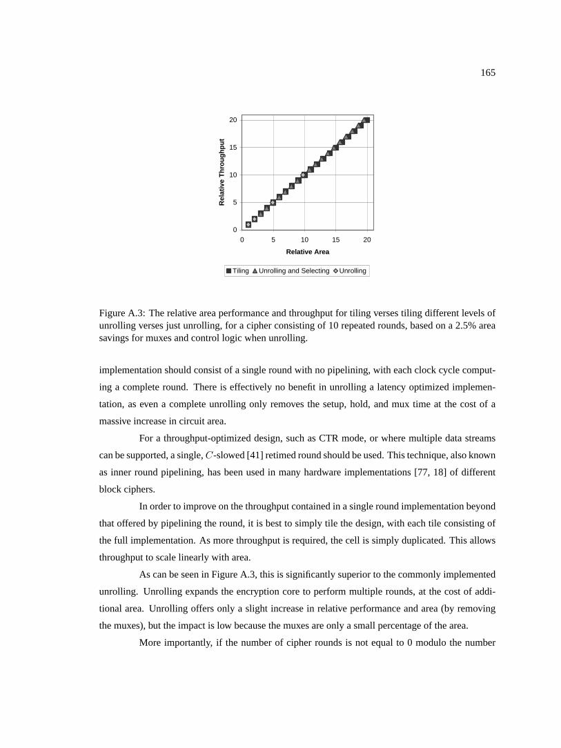
165
0
5
10
15
20
0 5 10 15 20
Relative Area
Rel
ativ
e T
hro
ug
hp
ut
Tiling Unrolling and Selecting Unrolling
Figure A.3: The relative area performance and throughput for tiling verses tiling different levels ofunrolling verses just unrolling, for a cipher consisting of 10 repeated rounds, based on a 2.5% areasavings for muxes and control logic when unrolling.
implementation should consist of a single round with no pipelining, with each clock cycle comput-
ing a complete round. There is effectively no benefit in unrolling a latency optimized implemen-
tation, as even a complete unrolling only removes the setup, hold, and mux time at the cost of a
massive increase in circuit area.
For a throughput-optimized design, such as CTR mode, or where multiple data streams
can be supported, a single,C-slowed [41] retimed round should be used. This technique, also known
as inner round pipelining, has been used in many hardware implementations [77, 18] of different
block ciphers.
In order to improve on the throughput contained in a single round implementation beyond
that offered by pipelining the round, it is best to simply tile the design, with each tile consisting of
the full implementation. As more throughput is required, the cell is simply duplicated. This allows
throughput to scale linearly with area.
As can be seen in Figure A.3, this is significantly superior to the commonly implemented
unrolling. Unrolling expands the encryption core to perform multiple rounds, at the cost of addi-
tional area. Unrolling offers only a slight increase in relative performance and area (by removing
the muxes), but the impact is low because the muxes are only a small percentage of the area.
More importantly, if the number of cipher rounds is not equal to 0 modulo the number
166
of unrolled rounds, the efficiency is seriously reduced because of wasted logic during the last iter-
ation through the cipher. Thus, unrolling is only good when the number of unrolled rounds equals
0 modulo the total number of rounds. This is especially difficult if a multiple-key-length AES
implementation is desired, as the different key lengths require different numbers of rounds.
Tiling the appropriate level of unrolled rounds to match the throughput requirements of-
fers only a very small benefit over simple tiling, while greatly increasing the complexity as now sev-
eral designs (a single round, and all unrolling such that the cipher rounds modulo unrolled rounds =
0) are required to be designed, implemented, and tested.
Similarly, since tiling can achieve arbitrary throughput by replication, encryption through-
put is not a good metric for performance oriented block cipher implementations in hardware. In-
stead, throughput/area or throughput/cost are much more representative as these reflect the actual
cost of an implementation.
A.5 Implementing AES in Hardware
The optimum hardware implementation for AES is a single round with agile subkey gen-
eration, as unrolling offers negligible benefits. Due to the reasonable size of AES subkey generation,
and the flexibility a key agile implementation allows, key agile implementations are preferable to
stored-key implementations. Since most applications require subkey generation, there is no reason
not to include a key agile subkey generation module.
If high throughput is desired, the single round and associated subkey generation should
be manually or automaticallyC-slowed. If the design either uses CTR mode or another parallel
mode, or multiple streams can be encrypted simultaniously, the high-throughput design should be
used. The pipelining greatly increases throughput without adding a major impact on the area. This
pipelining can either be performed manually, as discussed in this chapter, or automated using tools
like the one described in Chapter 13. If low latency is required, the additional pipeline stages should
be removed to create a low-latency, rather than high-throughput implementation.
If the implementation technology supports ROMs (such as ASICs) or embedded prepro-
grammed RAMs (such as many FPGAs including the Virtex), they should be used to implement the
S-boxes. If the memories are larger than what is required to store the S-boxes, portions of the Galois
multiplications from the mix-column should be rolled into the design. Otherwise, if the implemen-
tation fabric doesn’t include embedded ROMs, techniques such as those in [56] should be used to
compose the S-boxes.

167
S-Boxes SubkeyXORs
DelayRegisters
SubkeyLoading/Producing
DelayRegisters
Subkey XORsand RCON
S-Boxes
Figure A.4: The Subkey Generation Implementation in a Xilinx Spartan II-100. Arrowheads are thelocation of pipeline stages, dataflow shown at 16 bit granularity.
In general, hand-layout offers significant performance benefits over HDL synthesis and
should be employed if high performance is desired. Often the best layout reflects the structure of
the cipher itself, with the data mostly kept in place and the operations applied. The only exception
is when the S-boxes need to be logically distinct from the rest of the design (as commonly seen in
Xilinx FPGAs, where the BlockRAMs are in separate columns), in which case a meet-in-the-middle
style structure may be appropriate.
A.6 AES Subkey Generation
Since the subkey generation depends on the key size, with the larger key sizes requiring
greater area, this core uses the 128 bit size, as this key-length is commonly usable while being more
compact than other implementations. Additionally, since fewer rounds are required, it offers greater
performance when compared with longer key lengths. This implementation is fully key-agile to
eliminate the time required for subkey setup and to eliminate the need for subkey storage. Since a
set of subkeys requires 176 bytes to store, the savings can be significant.
This implementation (Figure A.4) loads the keys in the center of the design and produces
128-bits of subkey after each pass through the pipeline. The subkey pieces are then passed to the
shift registers (SRL16s), with the one 32-bit quantity being word rotated and passed to registers in
front of the BlockRAMs used to implement the S-boxes. Due to the time required for communi-
cation, a register is placed to register the S-box inputs. Because of the considerable clk→q delay
on the BlockRAMs, the outputs are also registered. The keys are then mixed together, registered,
then transfered back to the middle. This meet-in-the-middle structure allows the rotation to occur
efficiently and matches the layout of the encryption core, which also includes a meet-in-the-middle
topology. The design effectively requires all of a 4 by 30 block of CLBs, requiring roughly 240
CLB slices and 2 BlockRAMs to implement.

168
This pipeline takes 5 stages to produce a set of subkeys, which matches the 5 stage pipelin-
ing required for the encryption core. For a latency optimized version, all pipeline stages except the
mandatory register in the BlockRAM and a single register for each intermediate value can be re-
moved, creating the low latency version.
A 192 or 256 bit implementation would be larger, because it requires retiming for either
6 or 8 32 bit subkeys. Additionally, it would require muxing the S-box inputs in order to handle the
slightly different rules involved in subkey generation. However, it would not slow down the rate at
which subkeys could be generated.
Although this implementation performs encryption only, a key-agile decryption core would
take roughly the same area by using the reverse S-boxes and inverse logic. Instead of accepting the
key, the last round’s subkeys are accepted and the process works in reverse. If the last set of subkeys
were not available (due to the structure of the protocol), a separate encryption subkey module could
be used to create the last set of subkeys, which are then stored or passed to the decryption module.
If a non-key-agile core were desired, replacing the 2 BlockRAMs and 240 slices would
provide 23 kb of storage. Since a single set of subkeys requires 1.4 kb to store, this could provide
enough storage for 16 sets of subkeys.
A.7 AES Encryption Core
The encryption core (Figure A.5) is structurally similar to the subkey core, but sparser, as
it is spread out over an 16 CLB high section to match the pitch of the BlockRAMs used to implement
the S-boxes. The general layout is very similar to the description: a 4x4 array of words which is
loaded in the middle. The left half of the array is processed on the left side, with the right half on
the right side. The input is XORed with the appropriate keys and loaded into muxes located next to
the S-boxes (area already used for pipeline registers).
The layout is pitch matched to the S-boxes, with each BlockRAM performing two simul-
taneous S-box lookups. Since the BlockRAMs are twice the size of the S-boxes, the Galois∗03
operation is also included, as needed for the Mix-Column step. Additionally, to improve the meet-
in-the-middle structure, the row-swap and S-box operations were exchanged. The Mix-Column step
uses the results of the S-box and S-box∗03 operation, computes the results∗02, and XORs them
together for each output word.
On the first cycle of the round, the data is moved from the registers in the middle to
registers on the periphery, next to the S-boxes. On the next cycle, the data is loaded into the S-
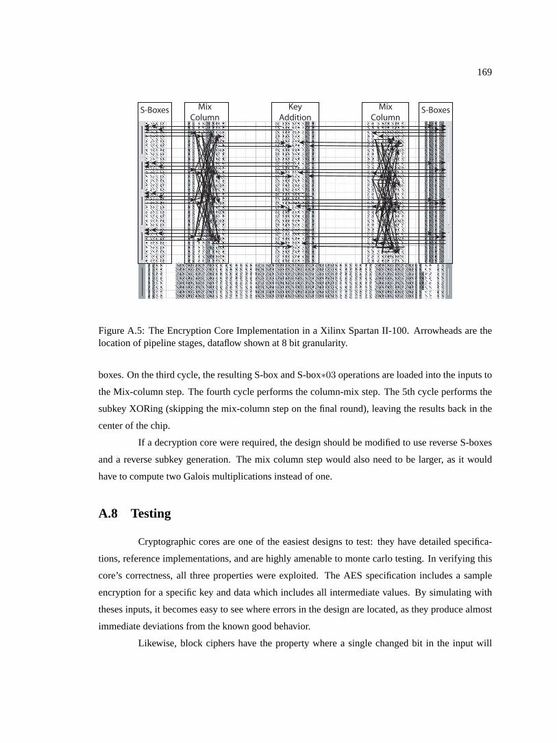
169
S-Boxes MixColumn
KeyAddition
MixColumn
S-Boxes
Figure A.5: The Encryption Core Implementation in a Xilinx Spartan II-100. Arrowheads are thelocation of pipeline stages, dataflow shown at 8 bit granularity.
boxes. On the third cycle, the resulting S-box and S-box∗03 operations are loaded into the inputs to
the Mix-column step. The fourth cycle performs the column-mix step. The 5th cycle performs the
subkey XORing (skipping the mix-column step on the final round), leaving the results back in the
center of the chip.
If a decryption core were required, the design should be modified to use reverse S-boxes
and a reverse subkey generation. The mix column step would also need to be larger, as it would
have to compute two Galois multiplications instead of one.
A.8 Testing
Cryptographic cores are one of the easiest designs to test: they have detailed specifica-
tions, reference implementations, and are highly amenable to monte carlo testing. In verifying this
core’s correctness, all three properties were exploited. The AES specification includes a sample
encryption for a specific key and data which includes all intermediate values. By simulating with
theses inputs, it becomes easy to see where errors in the design are located, as they produce almost
immediate deviations from the known good behavior.
Likewise, block ciphers have the property where a single changed bit in the input will

170
result in a massive number of changes in the output, the “avalanche” property. To exploit this for
testing, the output of the cipher is used as both the key and data for the next round of input. The
reference code is also run in the same mode, with any difference between the reference and the
design being debugged would be immediately noticed, as even a single bit error anywhere in the
core would quickly cascade resulting in vastly different results for the outputs of the reference and
the tested design.
During testing, almost all bugs were actually trapped during the detailed, part by part
encryption test, but the monte carlo test provided excellent verification of the initial debugging
process.
A.9 Performance
This design was implemented on both a Spartan-II 100-5 and a Virtex-E 600-8, using
Xilinx Foundation 4.1 tools. The Spartan II is fabricated in a .22µm process and is optimized for
low cost and low silicon area, while the Virtex-E is fabricated in a .18µm process and is optimized
for performance. They are functionally identical in the basic structure, although the Virtex-E parts
have additional memories, and the design was only modified slightly in placement between the two
parts. All toolflows were maximum effort, with timing reported by static timing analysis.
In order to provide the performance of a latency optimized version, all pipeline stages
were removed except for the mandatory stage for the BlockRAM. This results in a design which
performs a round per clock cycle, albeit with a slower clock. This removes the penalty for additional
setup and hold times, as well as eliminates the effects of unbalanced pipeline stages.
The performance, as summarized in Table A.1, is very impressive. Even on the low cost
part, a throughput-oriented implementation provides 1.3 Gbps throughput for non-feedback modes
(CBCk where k≥ 5, ECB, and CTR modes), while the latency optimized version provides 500
Mbps regardless of the feedback mode. Virtex-E provides, as expected, performance improvements
due to its faster operation.
A.10 Other implementations
Tables A.2 and A.3 have an summary of various reported hardware implementations, their
throughput, and their area cost. Both the Amphion [7] and Helion [32] are commercially available
IP cores which have been mapped to both Virtex series FPGAs and standard cell processes. Both
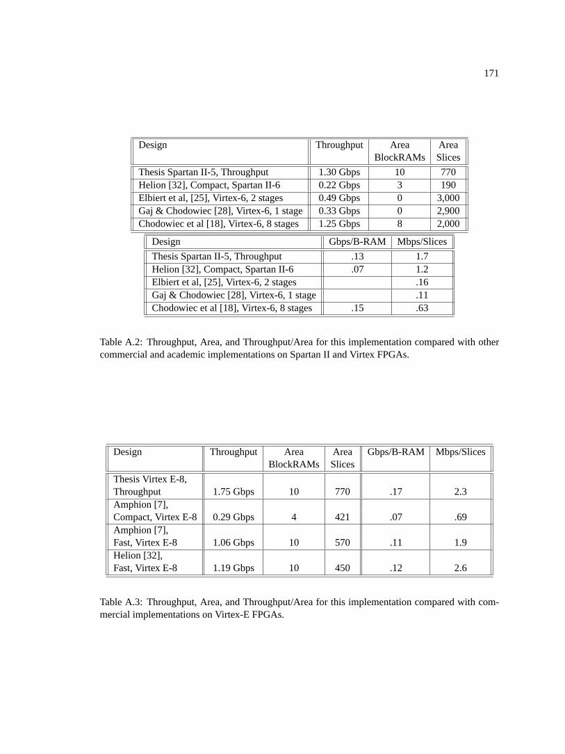
171
Design Throughput Area AreaBlockRAMs Slices
Thesis Spartan II-5, Throughput 1.30 Gbps 10 770Helion [32], Compact, Spartan II-6 0.22 Gbps 3 190Elbiert et al, [25], Virtex-6, 2 stages 0.49 Gbps 0 3,000Gaj & Chodowiec [28], Virtex-6, 1 stage 0.33 Gbps 0 2,900Chodowiec et al [18], Virtex-6, 8 stages 1.25 Gbps 8 2,000
Design Gbps/B-RAM Mbps/Slices
Thesis Spartan II-5, Throughput .13 1.7Helion [32], Compact, Spartan II-6 .07 1.2Elbiert et al, [25], Virtex-6, 2 stages .16Gaj & Chodowiec [28], Virtex-6, 1 stage .11Chodowiec et al [18], Virtex-6, 8 stages .15 .63
Table A.2: Throughput, Area, and Throughput/Area for this implementation compared with othercommercial and academic implementations on Spartan II and Virtex FPGAs.
Design Throughput Area Area Gbps/B-RAM Mbps/SlicesBlockRAMs Slices
Thesis Virtex E-8,Throughput 1.75 Gbps 10 770 .17 2.3Amphion [7],Compact, Virtex E-8 0.29 Gbps 4 421 .07 .69Amphion [7],Fast, Virtex E-8 1.06 Gbps 10 570 .11 1.9Helion [32],Fast, Virtex E-8 1.19 Gbps 10 450 .12 2.6
Table A.3: Throughput, Area, and Throughput/Area for this implementation compared with com-mercial implementations on Virtex-E FPGAs.
172
compact cores are sub-round implementation with microcoded datapaths, while both high speed
implementations are a single round (with unspecified pipelining) and include subkey generation.
The Amphion core uses a highly opitimzed HDL implementation which is synthesized
and retargeted for both Virtex, Altera, and standard cell models, while the Helion core is heavily
specialized to the Virtex architecture using unstated, architecture specific optimizations. As a result,
the Helion core shows greater performance in the same area. When compared with this chapter’s
core, the Helion fast core (which has the best performance of the available commercial implemen-
tations) actually gets better performance/slice, but worse performance/BlockRAM and worse total
performance for a single round when compared to this chapter’s implementation.
Three academic implementations have been reported, using HDL synthesis, targeting a
Virtex-6 speedgrade part. The Virtex parts targeted are only slightly faster than the Spartan II used
for this core, so it can be directly compared with out Spartan II numbers. None of these implemen-
tations included subkey generation, and all used HDL synthesis, where a language specified design
is compiled to the target architecture. The first, by Elbiert et al, [25], included several design points.
The optimal throughput per area implementation reported for a single round was a 2 stage pipeline,
using 3000 slices, without taking advantage of the BlockRAMs. It offered about 500 Mbps through-
put. The second, by Gaj & Chodowiec [28], was a similar structure but without any pipelining. As
expected, it only gets 330 Mbps throughput, while still requiring 2900 slices.
The third, a revision of the second version, by Chodowiec et al [18], used an 8 stage
pipeline. It is the HDL implementation which is most comparable to the benchmark implementation
used in this thesis, as the target is very comparable to the Spartan II and is aggressively pipelined.
Although it achieves a comparable (albeit slightly slower) throughput, it requires over twice the
number of slices due to the inefficiencies of HDL synthesis and requires an 8 stage pipeline instead
of a 5 stage pipeline to achieve the same performance.
A.11 Reflections
By careful use of hand mapping and selection, pipelining, and target specific optimiza-
tions, one can produce compact, high performance AES implementations on FPGAs. 1.3 Gbps on
nonfeedback modes, or 500 Mbps on feedback modes, are generally achievable on very low cost
FPGAs such as the Spartan II 100, using 10 BlockRAMs and 770 slices. The throughput-oriented
implementations can be scaled to arbitrary throughput by simple tiling. Making the implementation
fully key-agile offers significant flexibility benefits while only adding a small area cost.
173
In general, applications such as AES are excellent choices for evaluating tools and archi-
tectures. A highly pipelined design can be compared with an unpipelined design which is automat-
ically C-slowed (as seen in Chapter 13, while the placement can be removed to evaluate the quality
of placement tools (discussed in Chapter 3).
For such experiments, there are substantial advantages in utilizing known important ap-
plications and kernels, as they are highly representative of real designs. The major disadvantage
is that the best results are achieved, as in this case, by careful optimization for a particular target
architecture. Thus these high quality benchmarks require significant implementer effort to create.
A.12 Summary
This appendix demonstrated the design techniques needed to create a high performance
design targeting a conventional FPGA. It shows that high performance designs, although possible,
require considerable effort to construct a good placement and a high performance pipeline. One of
the primary goals of a fixed-frequency architecture is to eliminate much of these efforts for high-
throughput designs, as the architecture and tools guarantee a throughput for all successfully mapped
designs.
The cryptographic example also illustrates the important distinction between latency and
throughput, how throughput can be arbitrarily scaled but latency reaches intrinsic limits, and how a
design optimized for throughput suffers from significantly worse latency. These themes will be re-
visited in Chapter 15, discussing the relationships between latency, throughput, and fixed-frequency
FPGAs.

174
Appendix B
Other Multithreaded Architectures
As seen in Chapter 11, automaticC-slowing of a microprocessor core can automatically
create a multithreaded processor architecture. This appendix reviews other multithreaded architec-
tures, their goals, and the various synergistic and interference effects which occur. TheC-slowed
architecture, and interleaved architectures in general, have fewer interference effects when com-
pared with an SMT (Symmetric Multithreaded) architecture.
B.1 Previous Multithreaded Architectures
The HEP [66] was the first major multithreaded architecture. The HEP processing node
uses a simple 8 stage pipeline without forwarding and a large register file. Every clock cycle,
instructions from a different thread are issued into the pipeline. The HEP design allows for a con-
siderable amount of latency to be hidden through multiple threads, but significantly impacts single
thread performance.
Tera [6] was an extension of the HEP architecture, designed to accommodate memory
access in the pipeline. The Tera processing node had no data caches, instead choosing to hide
memory latency by switching to other threads. Although effective at hiding memory latency, nearly
70 threads are required to fully utilize a processing node on memory-intensive tasks.
“Context switching on event” has also been used to hide memory latency, in systems such
as the Intel IXP 1200 [35] network processor. The other operations in each microcoded core requires
only a single cycle, but memory may take many cycles. In order to hide memory latency, the core
will context-switch to one of three other threads, when there is a memory miss.
Interleaved Multithreading [40] was proposed as a compromise technique between the
175
“no bypassing” of HEP and Tera and the “context switch on cache-miss” semantics used in the IXP
and others. This mechanism had 2 or more threads executing in a round-robin fashion, with the goal
of having more memory requests outstanding as each thread would be issuing independent requests
without incurring the context switch penalty on memory miss.
The interleaved architecture was justified because context-switching on a memory miss
introduces bubbles into the pipeline which result in a loss of efficiency. The interleaved model never
took advantage of the increased pipeline opportunities to gain higher overall throughput.
A different multithreaded approach, symmetric multithreaded, was developed initially
by at the University of Washington [75]. This approach modifies the issue rules and register file
of a wide superscalar architecture to issue from multiple threads simultaneously. This requires
modifying the issue logic, retirement logic, increasing the register file, and some other assorted
changes. SMT does not result in an improved clock frequency.
This techniques is highly productive to modifying a wide superscalar, as such architec-
tures tend to waste many of the available issues slots. The measured efficiency is claimed to better
than comparable superscalar, shared die SMP, or multithreaded architectures. If one also modifies
the translation and interrupt handling, one can create an SMP style programming model.
SMT offers several advantages: with a comparatively minor addition in complexity it
offers significant benefits in throughput while having a low effect on single thread throughput. Un-
fortunately, SMT is only applicable to wide superscalar architectures where there exists a consider-
able number of unused functional units. So, although the technique itself adds comparatively little
complexity, it is only applicable to highly complex architectures.
Intel has commercialized a 2-thread version based on the Pentium 4 core [36], creating a
design with 2 logical processors contained within a single physical processor. Intel has not released
many details about the internal architecture, but has reported that all architectural state (including
segment and interrupt registers) is duplicated to create an SMP programming model. Intel uses the
term “Hyperthreaded” rather than SMT.
An additional, backwards-compatiblepause instruction is added to insure that spin-
loops do not consume resources which could be devoted to the other virtual processor, while a
halt instruction should be added to the OS idle loop. Intel did not increase the number of physical
registers in the design. Since the P4 core uses register renaming, mapping 8 architectural registers
to 128 physical registers, there is really no need to increase the size of the register file when creating
an SMT based on the P4 core, although this adds another potential point-of-contention between the
two threads.
176
B.2 Synergistic and interference effects
Anytime a multithreaded architecture shares resources between threads, there is a poten-
tial for interference or synergistic effects. Interference effects, where the two threads degrade each
others performance, are more common, as synergistic effects can only occur when the independent
threads benefit from shared results.
For all the multithreaded architectures, these effects will show up in memory behavior.
SMT has additional interference effects with functional-unit congestion and physical register limi-
tations. The most substantial effects occur in the cache and memory, where the different working
sets interact. The traditional cache miss sources, compulsory, capacity, conflict, and coherency, also
need to includeincoherancywhen discussing multithreaded systems.
In a conventional multiprocessor, when two processors share a working set, this will often
create coherency misses as the writes of one processor are forced to update or invalidate the other’s
cache entries. The opposite occurs on a multithreaded architecture, as a disjoint working set will
cause significantly more pressure on the cache, while a common working set will provide synergistic
benefits as the two threads will share the working set, reducing the cache misses. These cache effects
will occur on both theC-slowed/interleaved architecture and on SMT architectures.
An SMT also has interference effects with the functional units and physical registers. As
an example, the SMT Pentium 4 retains the same number of functional units and physical registers,
so when operating in multithreaded mode the two threads compete for the same resources. Since
threadsnevershare registers (allowing sharing breaks the programming model of two independent
processors), this can only degrade performance if the combined load of both threads requires more
than 128 physical registers to achieve maximum throughput.
Likewise, two floating-point intensive tasks on an SMT will interfere substantially, as they
are competing for access to the same functional units, an effect which would not occur if the two
tasks used different resources.
These register and functional-unit effects do not occur on an interleaved orC-slowed
architecture, as each thread is allocated exclusive access to all functional units. Thus each thread is
guaranteed access to these resources, whether or not the other task desires similar access.