the short channel mosfet dr. lynn fuller - rit - people short channel mosfet page 1 the short...
TRANSCRIPT
© March 21, 2009 Dr. Lynn Fuller, Professor
Rochester Institute of TechnologyMicroelectronic Engineering
The Short Channel MOSFET
Page 1
The Short Channel MOSFET
Dr. Lynn Fuller Webpage: http://people.rit.edu/lffeee Microelectronic Engineering
Rochester Institute of Technology 82 Lomb Memorial Drive Rochester, NY 14623-5604 Tel (585) 475-2035 Fax (585) 475-5041
Email: [email protected] Department Webpage: http://www.microe.rit.edu
3-21-2009 MOSFET_S.PPT
ROCHESTER INSTITUTE OF TECHNOLOGYMICROELECTRONIC ENGINEERING
© March 21, 2009 Dr. Lynn Fuller, Professor
Rochester Institute of TechnologyMicroelectronic Engineering
The Short Channel MOSFET
Page 2
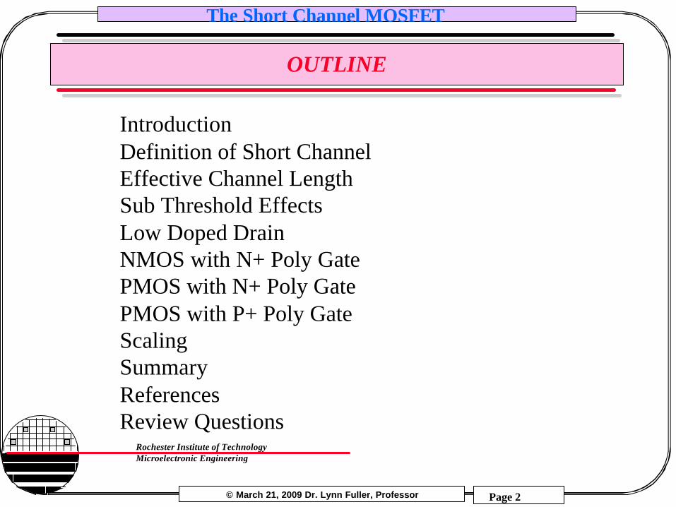
OUTLINE
IntroductionDefinition of Short ChannelEffective Channel LengthSub Threshold EffectsLow Doped DrainNMOS with N+ Poly GatePMOS with N+ Poly GatePMOS with P+ Poly GateScalingSummaryReferencesReview Questions
© March 21, 2009 Dr. Lynn Fuller, Professor
Rochester Institute of TechnologyMicroelectronic Engineering
The Short Channel MOSFET
Page 3
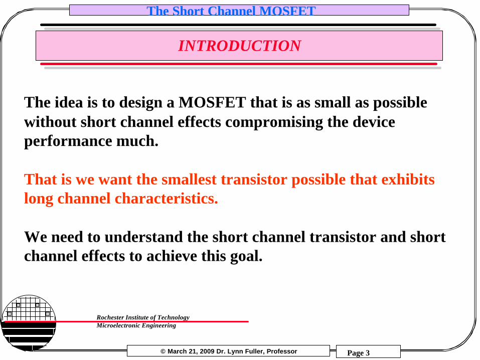
INTRODUCTION
The idea is to design a MOSFET that is as small as possible without short channel effects compromising the device performance much.
That is we want the smallest transistor possible that exhibits long channel characteristics.
We need to understand the short channel transistor and short channel effects to achieve this goal.
© March 21, 2009 Dr. Lynn Fuller, Professor
Rochester Institute of TechnologyMicroelectronic Engineering
The Short Channel MOSFET
Page 4
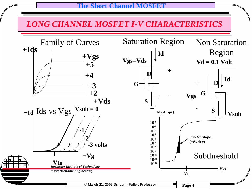
LONG CHANNEL MOSFET I-V CHARACTERISTICS
Id (Amps)
10-5
VgsVt
Sub Vt Slope (mV/dec)
10-410-310-2
10-1010-910-810-710-6
10-11
10-12
G
D
S
Vgs=VdsId
+
-
+Ids+Vgs
+Vds
+5+4+3+2
+Vg
+Id
Vto
Vsub = 0
-2-1
-3 volts
G
D
S
Vgs
Id+
-Vsub
Vd = 0.1 Volt
Family of Curves
Ids vs Vgs
Subthreshold
Saturation Region Non SaturationRegion
© March 21, 2009 Dr. Lynn Fuller, Professor
Rochester Institute of TechnologyMicroelectronic Engineering
The Short Channel MOSFET
Page 5
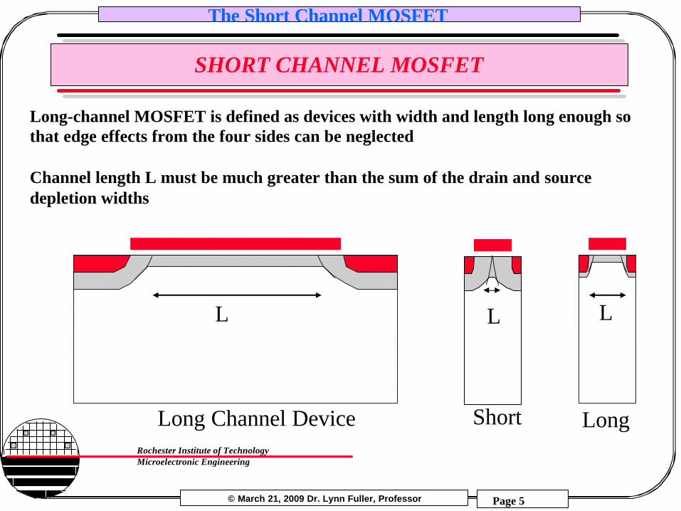
SHORT CHANNEL MOSFET
Long-channel MOSFET is defined as devices with width and length long enough so that edge effects from the four sides can be neglected
Channel length L must be much greater than the sum of the drain and source depletion widths
L L L
Long Channel Device Short Long
© March 21, 2009 Dr. Lynn Fuller, Professor
Rochester Institute of TechnologyMicroelectronic Engineering
The Short Channel MOSFET
Page 6
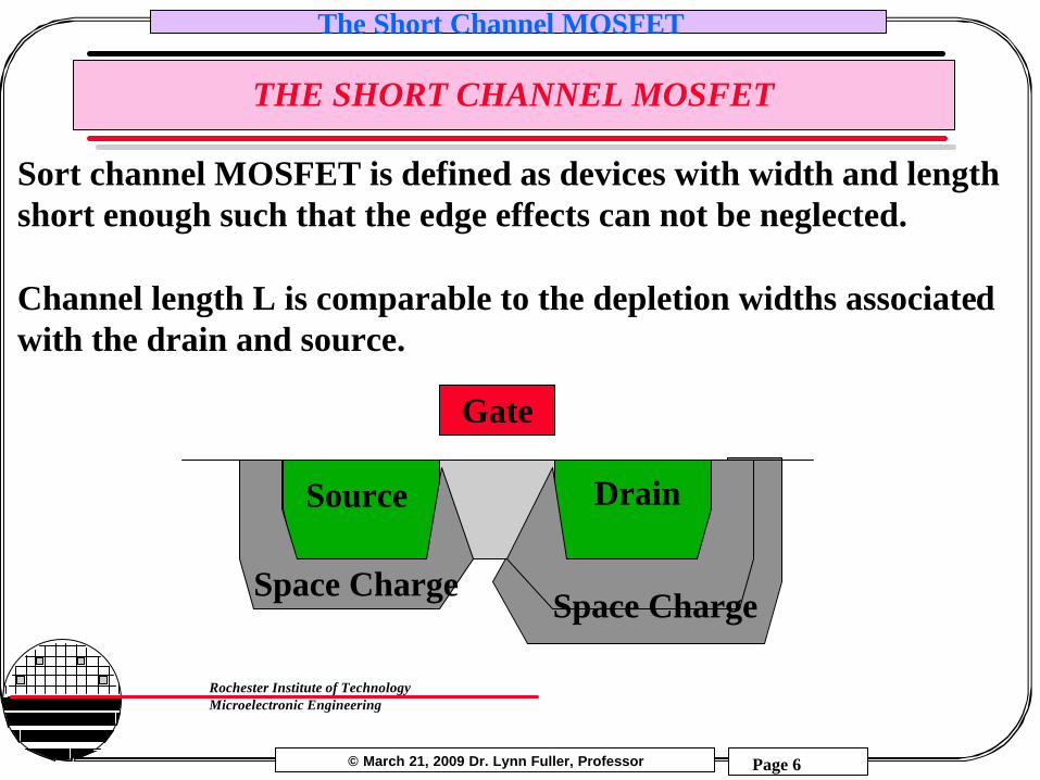
THE SHORT CHANNEL MOSFET
Sort channel MOSFET is defined as devices with width and length short enough such that the edge effects can not be neglected.
Channel length L is comparable to the depletion widths associated with the drain and source.
Gate
Source Drain
Space ChargeSpace Charge
© March 21, 2009 Dr. Lynn Fuller, Professor
Rochester Institute of TechnologyMicroelectronic Engineering
The Short Channel MOSFET
Page 7
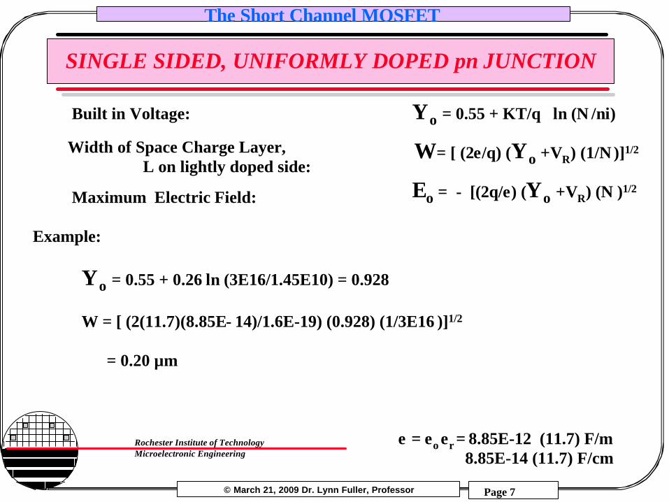
SINGLE SIDED, UNIFORMLY DOPED pn JUNCTION
W= [ (2ε/q) (Ψο +VR) (1/N )]1/2
Εο = - [(2q/ε) (Ψο +VR) (N )1/2
Ψο = 0.55 + KT/q ln (N /ni)Built in Voltage:
Width of Space Charge Layer, L on lightly doped side:
Example:
Maximum Electric Field:
ε = εo εr = 8.85E-12 (11.7) F/m8.85E-14 (11.7) F/cm
Ψο = 0.55 + 0.26 ln (3E16/1.45E10) = 0.928
W = [ (2(11.7)(8.85Ε−14)/1.6E-19) (0.928) (1/3E16 )]1/2
= 0.20 µm
© March 21, 2009 Dr. Lynn Fuller, Professor
Rochester Institute of TechnologyMicroelectronic Engineering
The Short Channel MOSFET
Page 8
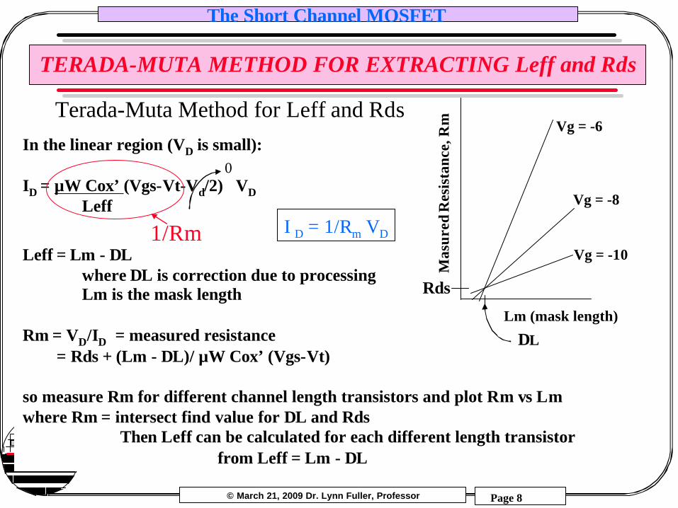
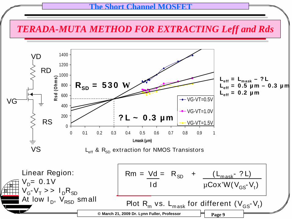
TERADA-MUTA METHOD FOR EXTRACTING Leff and Rds
In the linear region (VD is small):
ID = µW Cox’ (Vgs-Vt-Vd/2) VDLeff
Leff = Lm - ∆L where ∆L is correction due to processingLm is the mask length
Rm = VD/ID = measured resistance= Rds + (Lm - ∆L)/ µW Cox’ (Vgs-Vt)
so measure Rm for different channel length transistors and plot Rm vs Lmwhere Rm = intersect find value for ∆L and Rds
Then Leff can be calculated for each different length transistorfrom Leff = Lm - ∆L
Vg = -6
Vg = -10
Vg = -8
Lm (mask length)
Mas
ured
Res
ista
nce,
Rm
∆L
Terada-Muta Method for Leff and Rds
Rds
I D = 1/Rm VD1/Rm
0
© March 21, 2009 Dr. Lynn Fuller, Professor
Rochester Institute of TechnologyMicroelectronic Engineering
The Short Channel MOSFET
Page 9
TERADA-MUTA METHOD FOR EXTRACTING Leff and Rds
Rm = Vd = RSD + (Lmask- ? L)µCox’W(VGS-Vt)Id
Plot Rm vs. Lmask for different (VGS-Vt)
Linear Region:VD= 0.1VVG-VT >> IDRSDAt low ID, VRSD small
0
200
400
600
800
1000
1200
1400
0 0.1 0.2 0.3 0.4 0.5 0.6 0.7 0.8 0.9 1
Lmask (µm)
Rsd
(O
hms)
VG-VT=0.5V
VG-VT=1.0V
VG-VT=1.5V
RSD = 530 Ω
? L ~ 0.3 µm
VG
VD
VS
RD
RS
Leff & RSD extraction for NMOS Transistors
Leff = Lmask – ? LLeff = 0.5 µm – 0.3 µmLeff = 0.2 µm
© March 21, 2009 Dr. Lynn Fuller, Professor
Rochester Institute of TechnologyMicroelectronic Engineering
The Short Channel MOSFET
Page 10
SHORT CHANNEL EFFECTS
Channel Length ModulationThreshold Voltage Roll-offNarrow Gate Width EffectsReverse Short Channel EffectsPunch ThroughMobility DegradationVelocity Saturation
© March 21, 2009 Dr. Lynn Fuller, Professor
Rochester Institute of TechnologyMicroelectronic Engineering
The Short Channel MOSFET
Page 11
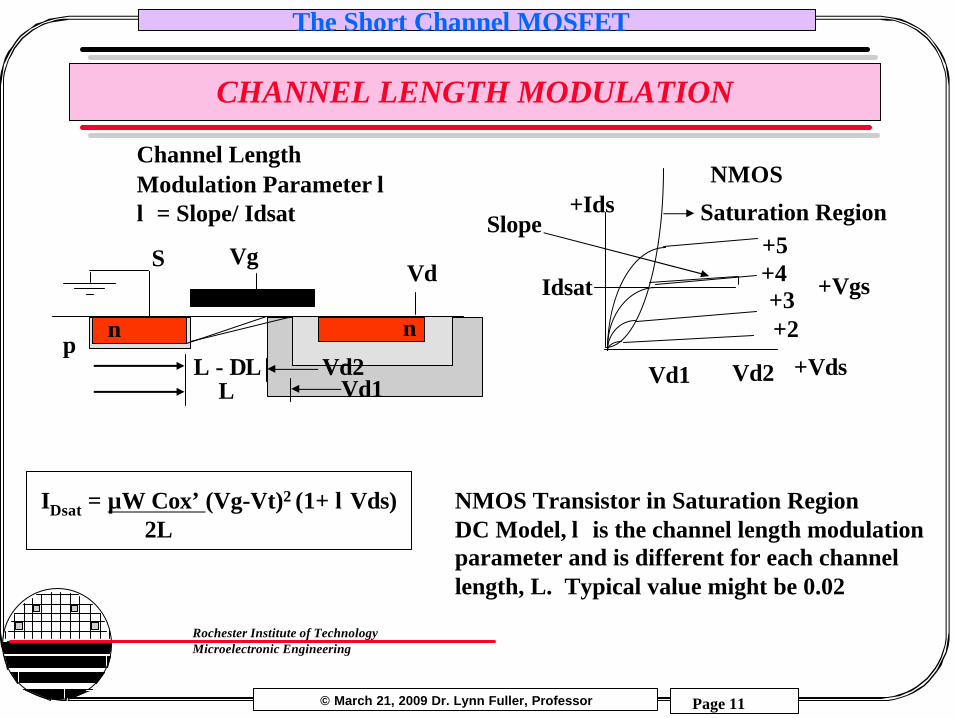
CHANNEL LENGTH MODULATION
IDsat = µW Cox’ (Vg-Vt)2 (1+ λVds) NMOS Transistor in Saturation Region2L DC Model, λ is the channel length modulation
parameter and is different for each channellength, L. Typical value might be 0.02
Channel Length Modulation Parameter λλ = Slope/ Idsat
n n
S VgVd
p
LL - ∆L
Vd1Vd2
Slope+Ids
+Vgs
+Vds
NMOS
+5+4+3+2
Saturation Region
Vd1 Vd2
Idsat
© March 21, 2009 Dr. Lynn Fuller, Professor
Rochester Institute of TechnologyMicroelectronic Engineering
The Short Channel MOSFET
Page 12
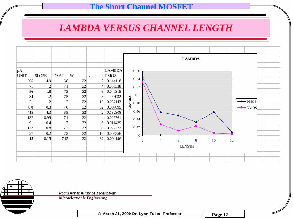
LAMBDA VERSUS CHANNEL LENGTH
µA LAMBDAUNIT SLOPE IDSAT W L PMOS NMOS
205 4.9 6.8 32 2 0.144118 0.13230871 2 7.1 32 4 0.056338 0.02676156 1.8 7.3 32 6 0.049315 0.01142934 1.2 7.5 32 8 0.032 0.02222221 2 7 32 16 0.057143 0.0055568.8 0.3 7.6 32 32 0.007895 0.004196415 4.3 6.5 32 2 0.132308137 0.95 7.1 32 4 0.02676191 0.4 7 32 6 0.011429
137 0.8 7.2 32 8 0.02222227 0.2 7.2 32 16 0.00555615 0.15 7.15 32 32 0.004196
LAMBDA
0
0.02
0.04
0.06
0.08
0.1
0.12
0.14
0.16
2 4 6 8 16 32
LENGTH
LA
MB
DA
PMOS
NMOS
© March 21, 2009 Dr. Lynn Fuller, Professor
Rochester Institute of TechnologyMicroelectronic Engineering
The Short Channel MOSFET
Page 13
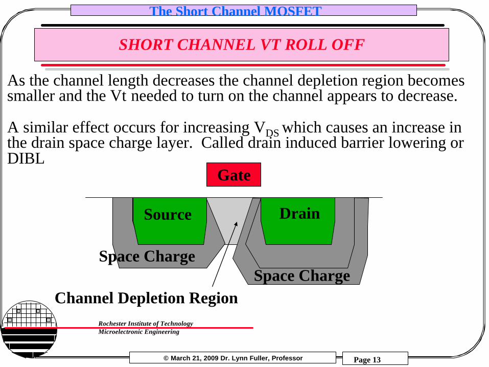
SHORT CHANNEL VT ROLL OFF
As the channel length decreases the channel depletion region becomes smaller and the Vt needed to turn on the channel appears to decrease.
A similar effect occurs for increasing VDS which causes an increase in the drain space charge layer. Called drain induced barrier lowering or DIBL
Gate
Space Charge
Channel Depletion Region
Drain
Space Charge
Source
© March 21, 2009 Dr. Lynn Fuller, Professor
Rochester Institute of TechnologyMicroelectronic Engineering
The Short Channel MOSFET
Page 14
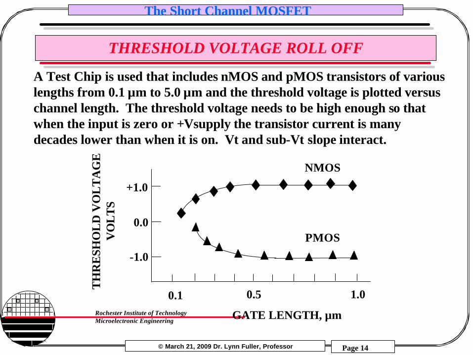
THRESHOLD VOLTAGE ROLL OFF
A Test Chip is used that includes nMOS and pMOS transistors of various lengths from 0.1 µm to 5.0 µm and the threshold voltage is plotted versus channel length. The threshold voltage needs to be high enough so that when the input is zero or +Vsupply the transistor current is many decades lower than when it is on. Vt and sub-Vt slope interact.
TH
RE
SHO
LD
VO
LT
AG
EV
OL
TS
0.5 1.00.1
+1.0
0.0
-1.0
NMOS
PMOS
GATE LENGTH, µm
© March 21, 2009 Dr. Lynn Fuller, Professor
Rochester Institute of TechnologyMicroelectronic Engineering
The Short Channel MOSFET
Page 15
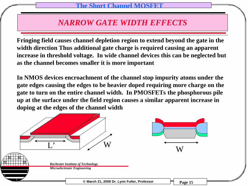
NARROW GATE WIDTH EFFECTS
Fringing field causes channel depletion region to extend beyond the gate in the width direction Thus additional gate charge is required causing an apparent increase in threshold voltage. In wide channel devices this can be neglected but as the channel becomes smaller it is more important
In NMOS devices encroachment of the channel stop impurity atoms under the gate edges causing the edges to be heavier doped requiring more charge on the gate to turn on the entire channel width. In PMOSFETs the phosphorous pile up at the surface under the field region causes a similar apparent increase in doping at the edges of the channel width
L’ W W
© March 21, 2009 Dr. Lynn Fuller, Professor
Rochester Institute of TechnologyMicroelectronic Engineering
The Short Channel MOSFET
Page 16
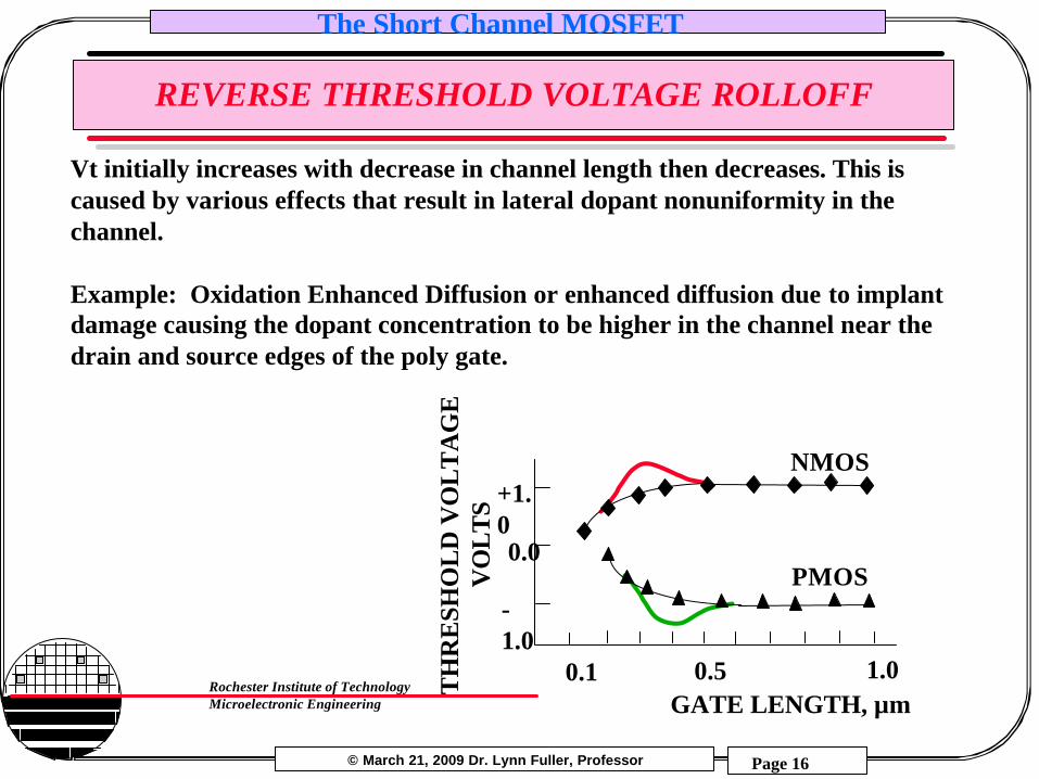
REVERSE THRESHOLD VOLTAGE ROLLOFF
Vt initially increases with decrease in channel length then decreases. This is caused by various effects that result in lateral dopant nonuniformity in the channel.
Example: Oxidation Enhanced Diffusion or enhanced diffusion due to implant damage causing the dopant concentration to be higher in the channel near the drain and source edges of the poly gate.
TH
RE
SHO
LD
VO
LT
AG
EV
OL
TS
0.5 1.00.1
+1.00.0
-1.0
NMOS
PMOS
GATE LENGTH, µm
© March 21, 2009 Dr. Lynn Fuller, Professor
Rochester Institute of TechnologyMicroelectronic Engineering
The Short Channel MOSFET
Page 17
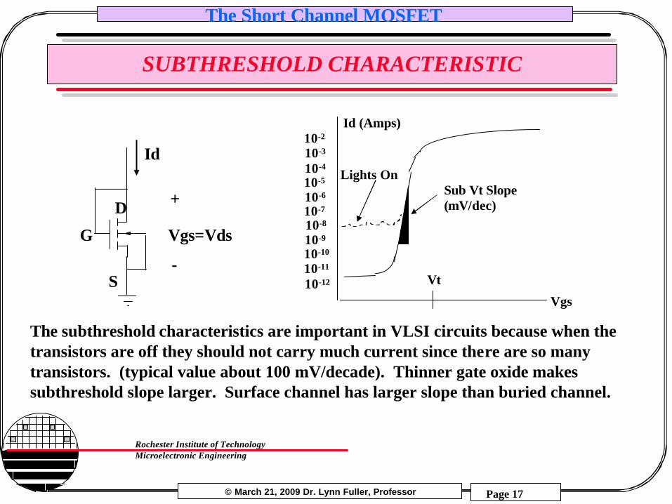
SUBTHRESHOLD CHARACTERISTIC
The subthreshold characteristics are important in VLSI circuits because when thetransistors are off they should not carry much current since there are so many transistors. (typical value about 100 mV/decade). Thinner gate oxide makes subthreshold slope larger. Surface channel has larger slope than buried channel.
Id (Amps)
10-5
Vgs
Vt
Sub Vt Slope (mV/dec)
10-410-310-2
10-1010-910-810-710-6
10-11
10-12
Lights On
G
D
S
Vgs=Vds
Id
+
-
© March 21, 2009 Dr. Lynn Fuller, Professor
Rochester Institute of TechnologyMicroelectronic Engineering
The Short Channel MOSFET
Page 18
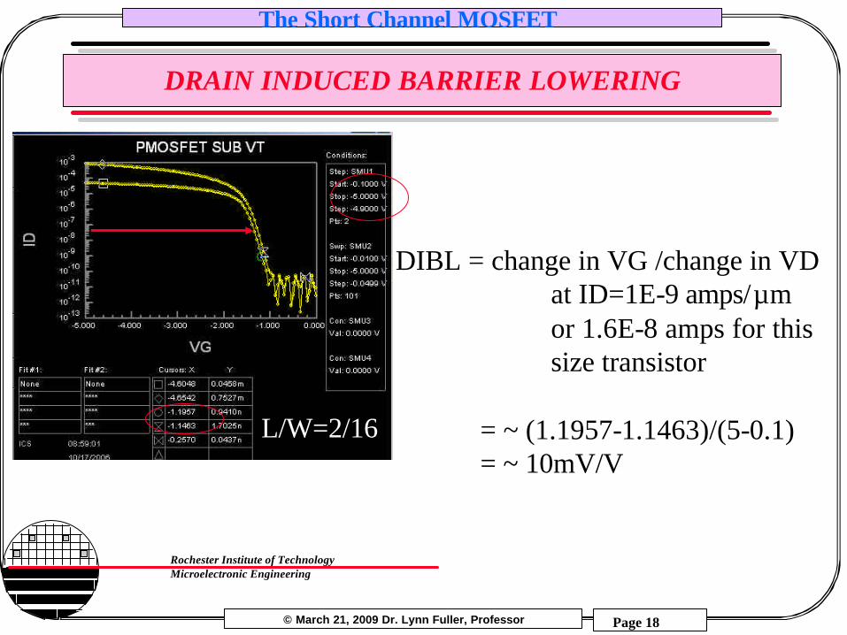
DRAIN INDUCED BARRIER LOWERING
DIBL = change in VG /change in VDat ID=1E-9 amps/µmor 1.6E-8 amps for thissize transistor
= ~ (1.1957-1.1463)/(5-0.1)= ~ 10mV/V
L/W=2/16
© March 21, 2009 Dr. Lynn Fuller, Professor
Rochester Institute of TechnologyMicroelectronic Engineering
The Short Channel MOSFET
Page 19
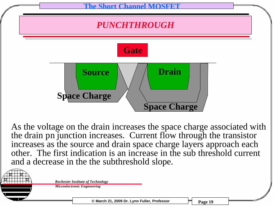
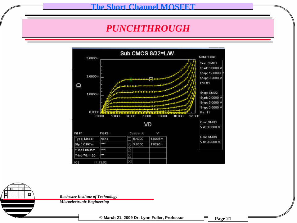
PUNCHTHROUGH
As the voltage on the drain increases the space charge associated with the drain pn junction increases. Current flow through the transistor increases as the source and drain space charge layers approach each other. The first indication is an increase in the sub threshold current and a decrease in the the subthreshold slope.
Gate
Space Charge
Drain
Space Charge
Source
© March 21, 2009 Dr. Lynn Fuller, Professor
Rochester Institute of TechnologyMicroelectronic Engineering
The Short Channel MOSFET
Page 20
PUNCHTHROUGH
Id (Amps)
10-5
VgsVt
Sub Vt Slope (mV/dec)
10-410-310-2
10-1010-910-810-710-6
10-11
10-12
Id (Amps)
10-5
VgsVt
Sub Vt Slope (mV/dec)
10-410-310-2
10-1010-910-810-710-6
10-11
10-12
Vds = 0.1
Vds =3
Vds = 6
Vds = 0.1
Vds =3
Vds = 6
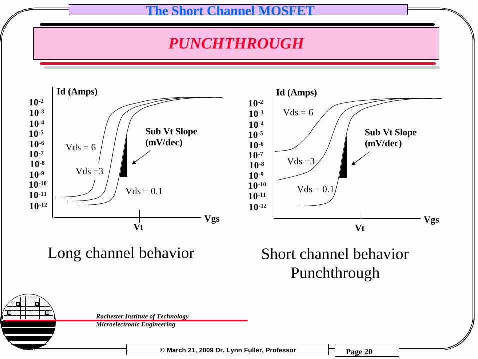
Long channel behavior Short channel behaviorPunchthrough
© March 21, 2009 Dr. Lynn Fuller, Professor
Rochester Institute of TechnologyMicroelectronic Engineering
The Short Channel MOSFET
Page 21
PUNCHTHROUGH
© March 21, 2009 Dr. Lynn Fuller, Professor
Rochester Institute of TechnologyMicroelectronic Engineering
The Short Channel MOSFET
Page 22
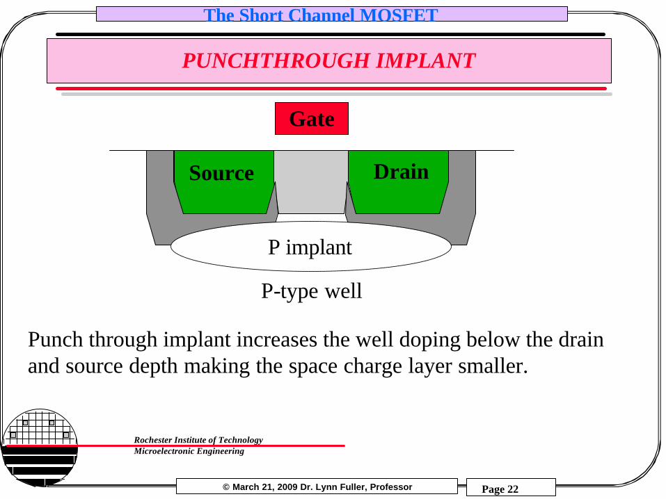
PUNCHTHROUGH IMPLANT
Gate
Source Drain
P implant
Punch through implant increases the well doping below the drain and source depth making the space charge layer smaller.
P-type well
© March 21, 2009 Dr. Lynn Fuller, Professor
Rochester Institute of TechnologyMicroelectronic Engineering
The Short Channel MOSFET
Page 23
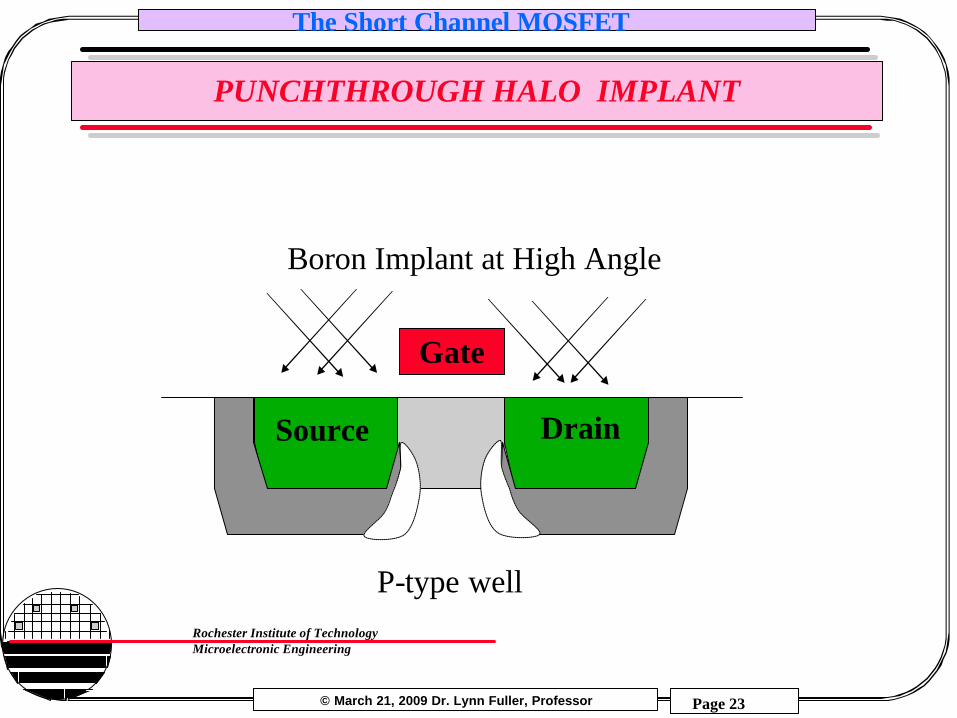
PUNCHTHROUGH HALO IMPLANT
Gate
Source Drain
Boron Implant at High Angle
P-type well
© March 21, 2009 Dr. Lynn Fuller, Professor
Rochester Institute of TechnologyMicroelectronic Engineering
The Short Channel MOSFET
Page 24
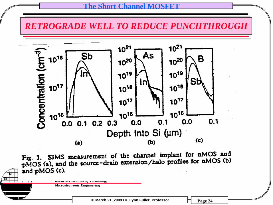
RETROGRADE WELL TO REDUCE PUNCHTHROUGH
© March 21, 2009 Dr. Lynn Fuller, Professor
Rochester Institute of TechnologyMicroelectronic Engineering
The Short Channel MOSFET
Page 25
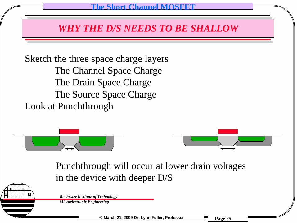
WHY THE D/S NEEDS TO BE SHALLOW
Sketch the three space charge layersThe Channel Space ChargeThe Drain Space ChargeThe Source Space Charge
Look at Punchthrough
Punchthrough will occur at lower drain voltages in the device with deeper D/S
© March 21, 2009 Dr. Lynn Fuller, Professor
Rochester Institute of TechnologyMicroelectronic Engineering
The Short Channel MOSFET
Page 26
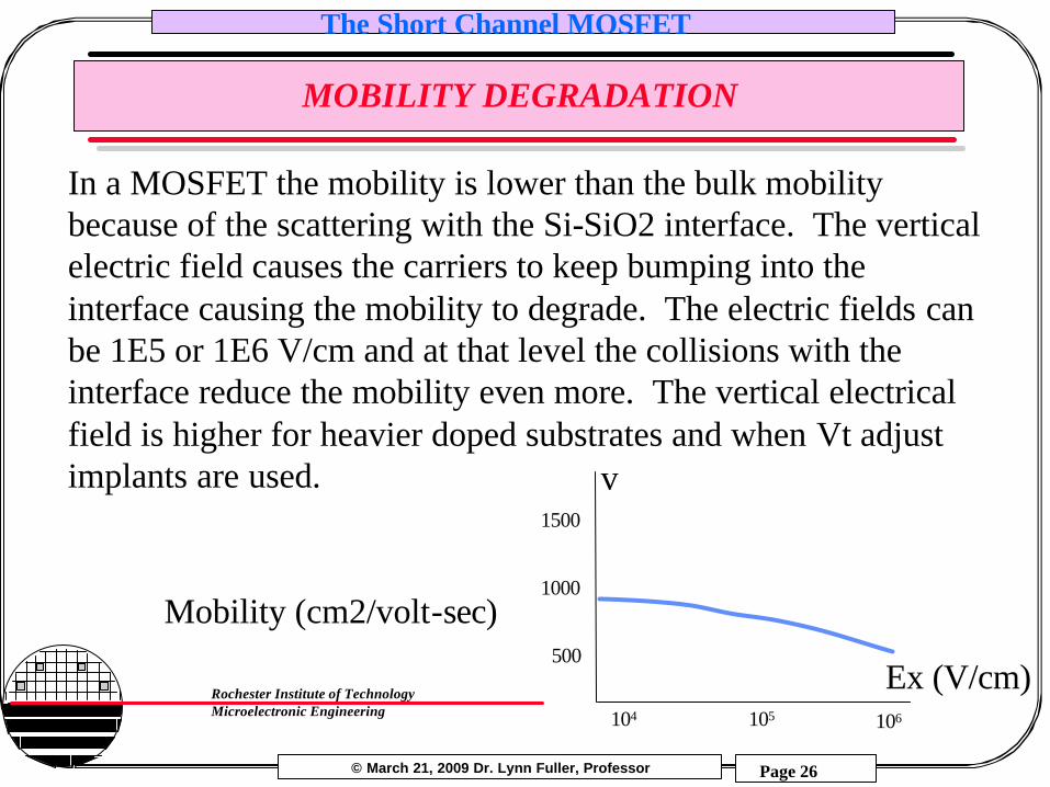
MOBILITY DEGRADATION
In a MOSFET the mobility is lower than the bulk mobility because of the scattering with the Si-SiO2 interface. The vertical electric field causes the carriers to keep bumping into the interface causing the mobility to degrade. The electric fields can be 1E5 or 1E6 V/cm and at that level the collisions with the interface reduce the mobility even more. The vertical electrical field is higher for heavier doped substrates and when Vt adjust implants are used.
Ex (V/cm)
v
Mobility (cm2/volt-sec)500
1500
1000
104 105 106
© March 21, 2009 Dr. Lynn Fuller, Professor
Rochester Institute of TechnologyMicroelectronic Engineering
The Short Channel MOSFET
Page 27
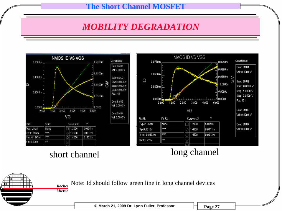
MOBILITY DEGRADATION
Note: Id should follow green line in long channel devices
short channel long channel
© March 21, 2009 Dr. Lynn Fuller, Professor
Rochester Institute of TechnologyMicroelectronic Engineering
The Short Channel MOSFET
Page 28
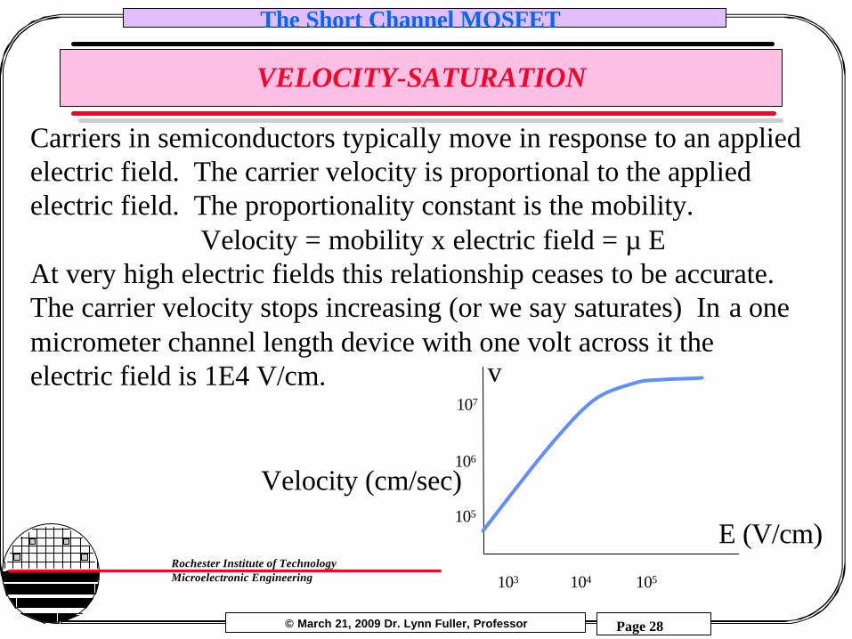
VELOCITY-SATURATION
Carriers in semiconductors typically move in response to an applied electric field. The carrier velocity is proportional to the applied electric field. The proportionality constant is the mobility.
Velocity = mobility x electric field = µ EAt very high electric fields this relationship ceases to be accurate. The carrier velocity stops increasing (or we say saturates) In a one micrometer channel length device with one volt across it the electric field is 1E4 V/cm.
E (V/cm)
v
Velocity (cm/sec)105
107
106
103 104 105
© March 21, 2009 Dr. Lynn Fuller, Professor
Rochester Institute of TechnologyMicroelectronic Engineering
The Short Channel MOSFET
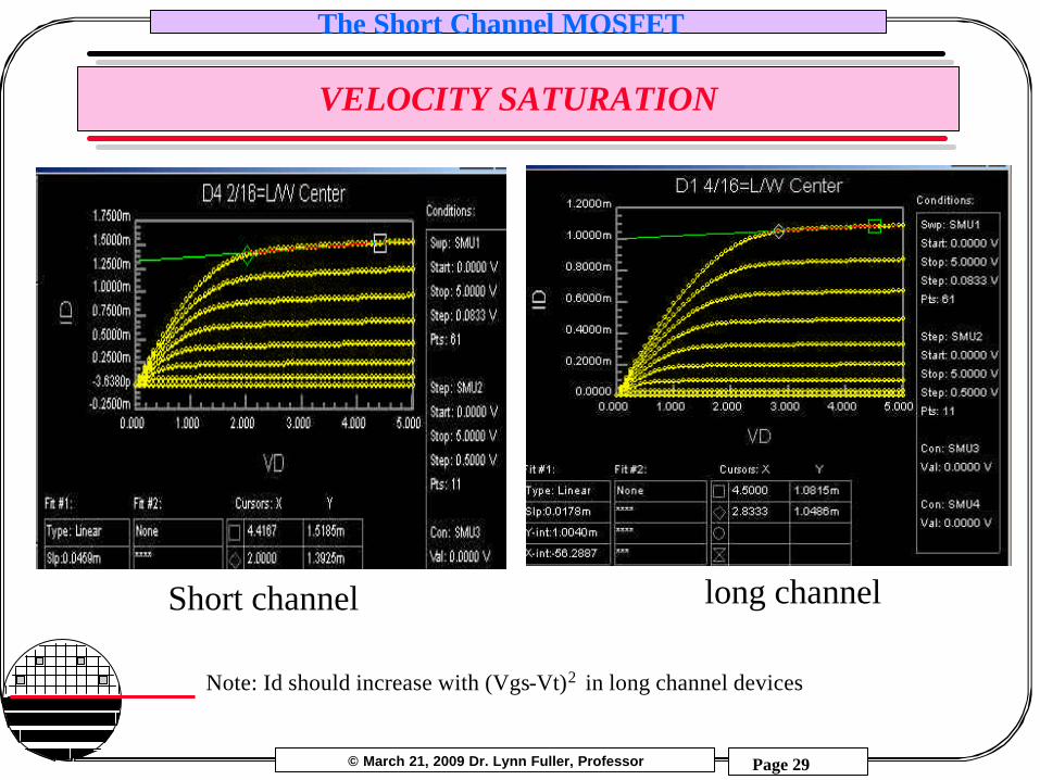
Page 29
VELOCITY SATURATION
Note: Id should increase with (Vgs-Vt)2 in long channel devices
Short channel long channel
© March 21, 2009 Dr. Lynn Fuller, Professor
Rochester Institute of TechnologyMicroelectronic Engineering
The Short Channel MOSFET
Page 30
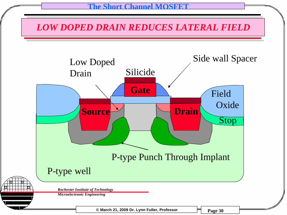
LOW DOPED DRAIN REDUCES LATERAL FIELD
Source
Gate
Drain
Side wall Spacer
FieldOxide
Stop
Low DopedDrain
P-type wellP-type Punch Through Implant
Silicide
© March 21, 2009 Dr. Lynn Fuller, Professor
Rochester Institute of TechnologyMicroelectronic Engineering
The Short Channel MOSFET
Page 31
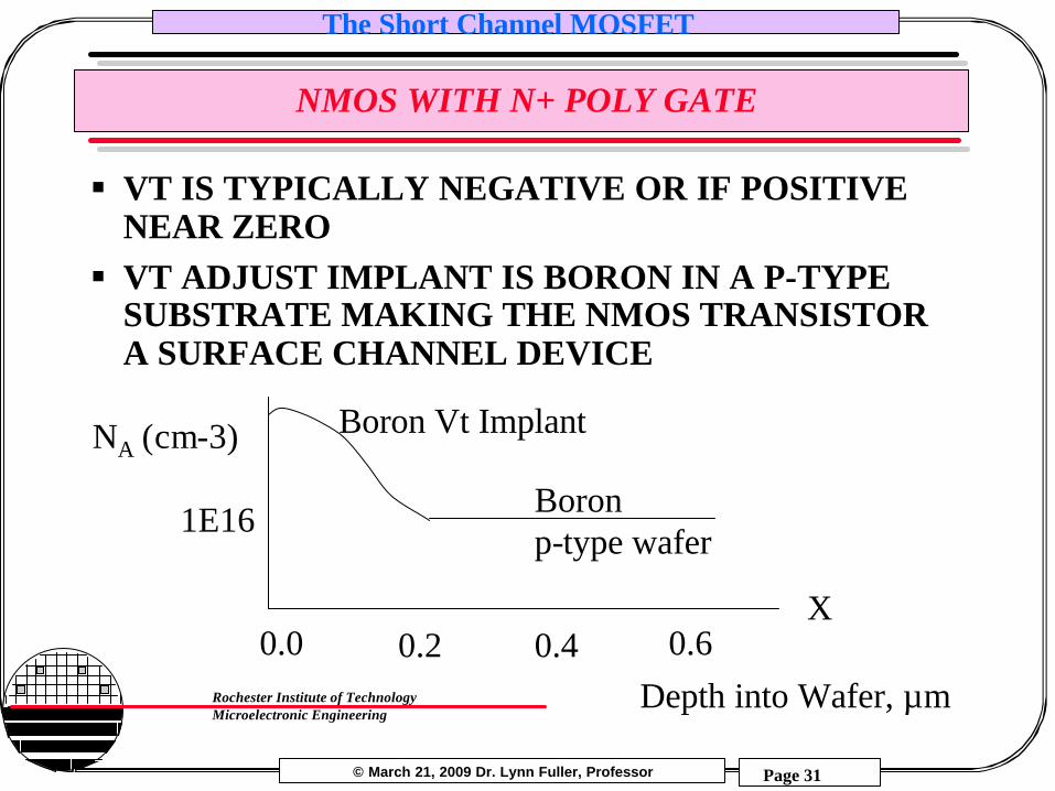
NMOS WITH N+ POLY GATE
§ VT IS TYPICALLY NEGATIVE OR IF POSITIVE NEAR ZERO§ VT ADJUST IMPLANT IS BORON IN A P-TYPE
SUBSTRATE MAKING THE NMOS TRANSISTOR A SURFACE CHANNEL DEVICE
1E16
NA (cm-3)
0.0 0.2 0.4 0.6X
Depth into Wafer, µm
Boronp-type wafer
Boron Vt Implant
© March 21, 2009 Dr. Lynn Fuller, Professor
Rochester Institute of TechnologyMicroelectronic Engineering
The Short Channel MOSFET
Page 32
PMOS WITH N+ POLY GATE
§ VT CAN NOT BE POSITIVE BECAUSE ALL THE CONTRIBUTORS TO THE VT ARE NEGATIVE. EVEN MAKING QSS=0 AND ND = ZERO DOES NOT MAKE VT POSITIVE
§ VT IS TYPICALLY MORE NEGATIVE THAN DESIRED LIKE -2 VOLTS
§ VT ADJUST IMPLANT IS BORON IN AN N-TYPE SUBSTRATE MAKING THE PMOS TRANSISTOR A BURIED CHANNEL DEVICE (CHARGE CARRIERS MOVE BETWEEN DRAIN AND SOURCE AT SOME DISTANCE AWAY FROM THE GATE OXIDE/SILICON INTERFACE
© March 21, 2009 Dr. Lynn Fuller, Professor
Rochester Institute of TechnologyMicroelectronic Engineering
The Short Channel MOSFET
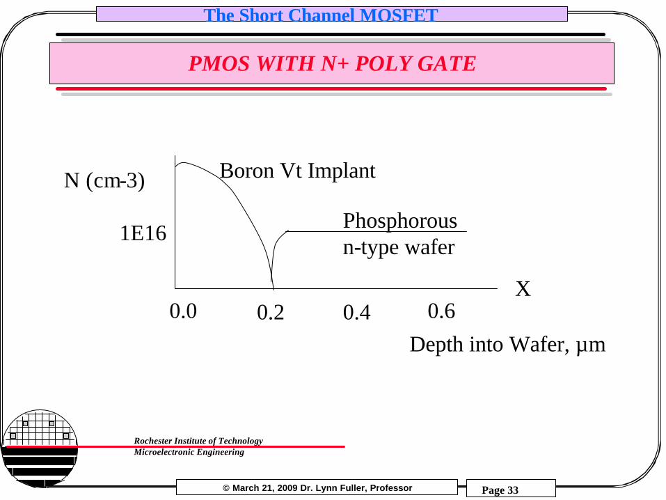
Page 33
PMOS WITH N+ POLY GATE
1E16
N (cm-3)
0.0 0.2 0.4 0.6X
Depth into Wafer, µm
Phosphorousn-type wafer
Boron Vt Implant
© March 21, 2009 Dr. Lynn Fuller, Professor
Rochester Institute of TechnologyMicroelectronic Engineering
The Short Channel MOSFET
Page 34
PMOS WITH P+ POLY GATE
§ CHANGES WORK FUNCTION OF THE METAL§ THUS METAL-SEMICONDUCTOR WORKFUNCTION
DIFFERERNCE BECOMES ABOUT +1 VOLT RATHER THAN ~0 VOLTS.
§ THIS MAKES VT MORE POSITIVE THAN DESIRED SO AN ION IMPLANT OF N-TYPE IMPURITY IS NEEDED MAKING THE DEVICE A SURFACE CHANNEL DEVICE RATHER THAN A BURIED CHANNEL DEVICE.
© March 21, 2009 Dr. Lynn Fuller, Professor
Rochester Institute of TechnologyMicroelectronic Engineering
The Short Channel MOSFET
Page 35
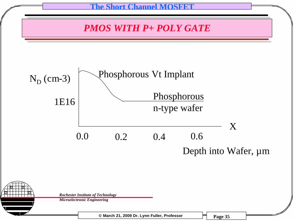
PMOS WITH P+ POLY GATE
1E16
ND (cm-3)
0.0 0.2 0.4 0.6X
Depth into Wafer, µm
Phosphorousn-type wafer
Phosphorous Vt Implant
© March 21, 2009 Dr. Lynn Fuller, Professor
Rochester Institute of TechnologyMicroelectronic Engineering
The Short Channel MOSFET
Page 36
SURFACE CHANNEL VS BURIED CHANNEL
§ SURFACE CHANNEL DEVICES EXHIBIT HIGHER SUBTHRESHOLD SLOPE§ SURFACE CHANNEL DEVICES ARE LESS
SENSITIVE TO PUNCH THROUGH§ SURFACE CHANNEL DEVICES HAVE LESS
SEVERE THRESHOLD VOLTAGE ROLLOFF§ SURFACE CHANNEL DEVICES HAVE HIGHER
TRANSCONDUCTANCE§ SURFACE CHANNEL DEVICES HAVE ABOUT
15% LOWER CARRIER MOBILITY
© March 21, 2009 Dr. Lynn Fuller, Professor
Rochester Institute of TechnologyMicroelectronic Engineering
The Short Channel MOSFET
Page 37
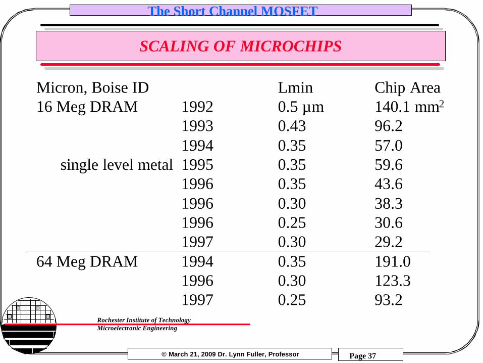
SCALING OF MICROCHIPS
Micron, Boise ID Lmin Chip Area16 Meg DRAM 1992 0.5 µm 140.1 mm2
1993 0.43 96.21994 0.35 57.0
single level metal 1995 0.35 59.61996 0.35 43.61996 0.30 38.31996 0.25 30.61997 0.30 29.2
64 Meg DRAM 1994 0.35 191.01996 0.30 123.31997 0.25 93.2
© March 21, 2009 Dr. Lynn Fuller, Professor
Rochester Institute of TechnologyMicroelectronic Engineering
The Short Channel MOSFET
Page 38
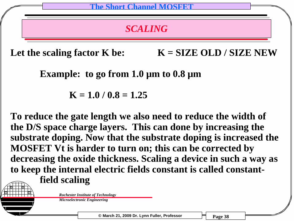
SCALING
Let the scaling factor K be: K = SIZE OLD / SIZE NEW
Example: to go from 1.0 µm to 0.8 µm
K = 1.0 / 0.8 = 1.25
To reduce the gate length we also need to reduce the width of the D/S space charge layers. This can done by increasing the substrate doping. Now that the substrate doping is increased theMOSFET Vt is harder to turn on; this can be corrected by decreasing the oxide thickness. Scaling a device in such a way as to keep the internal electric fields constant is called constant-
field scaling
© March 21, 2009 Dr. Lynn Fuller, Professor
Rochester Institute of TechnologyMicroelectronic Engineering
The Short Channel MOSFET
Page 39
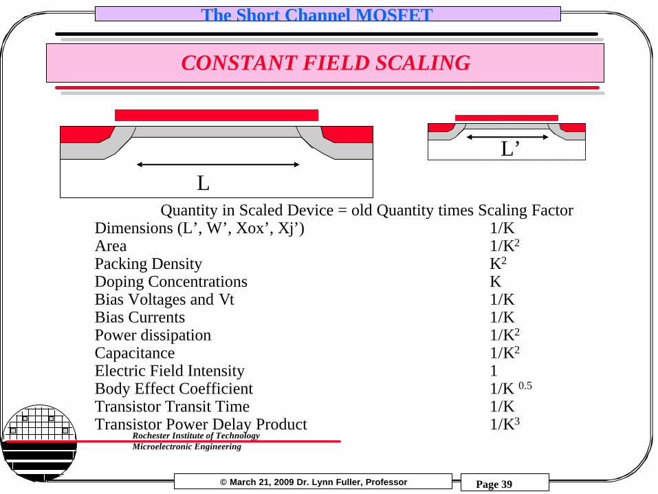
CONSTANT FIELD SCALING
L
L’
Quantity in Scaled Device = old Quantity times Scaling FactorDimensions (L’, W’, Xox’, Xj’) 1/KArea 1/K2
Packing Density K2
Doping Concentrations KBias Voltages and Vt 1/KBias Currents 1/KPower dissipation 1/K2
Capacitance 1/K2
Electric Field Intensity 1Body Effect Coefficient 1/K 0.5
Transistor Transit Time 1/KTransistor Power Delay Product 1/K3
© March 21, 2009 Dr. Lynn Fuller, Professor
Rochester Institute of TechnologyMicroelectronic Engineering
The Short Channel MOSFET
Page 40
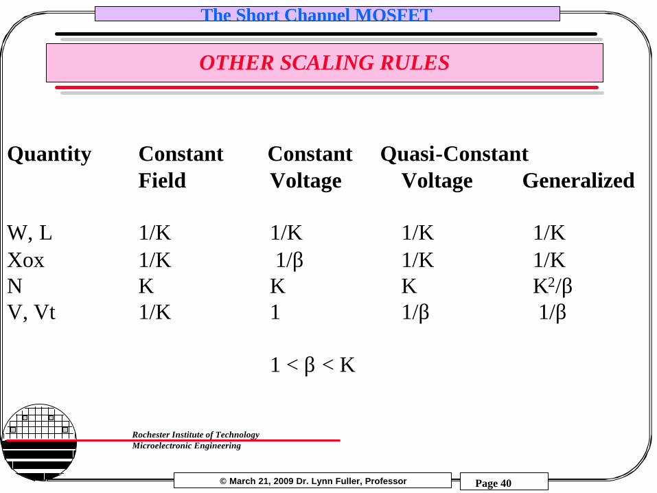
OTHER SCALING RULES
Quantity Constant Constant Quasi-Constant Field Voltage Voltage Generalized
W, L 1/K 1/K 1/K 1/KXox 1/K 1/β 1/K 1/KN K K K K2/βV, Vt 1/K 1 1/β 1/β
1 < β < K
© March 21, 2009 Dr. Lynn Fuller, Professor
Rochester Institute of TechnologyMicroelectronic Engineering
The Short Channel MOSFET
Page 41
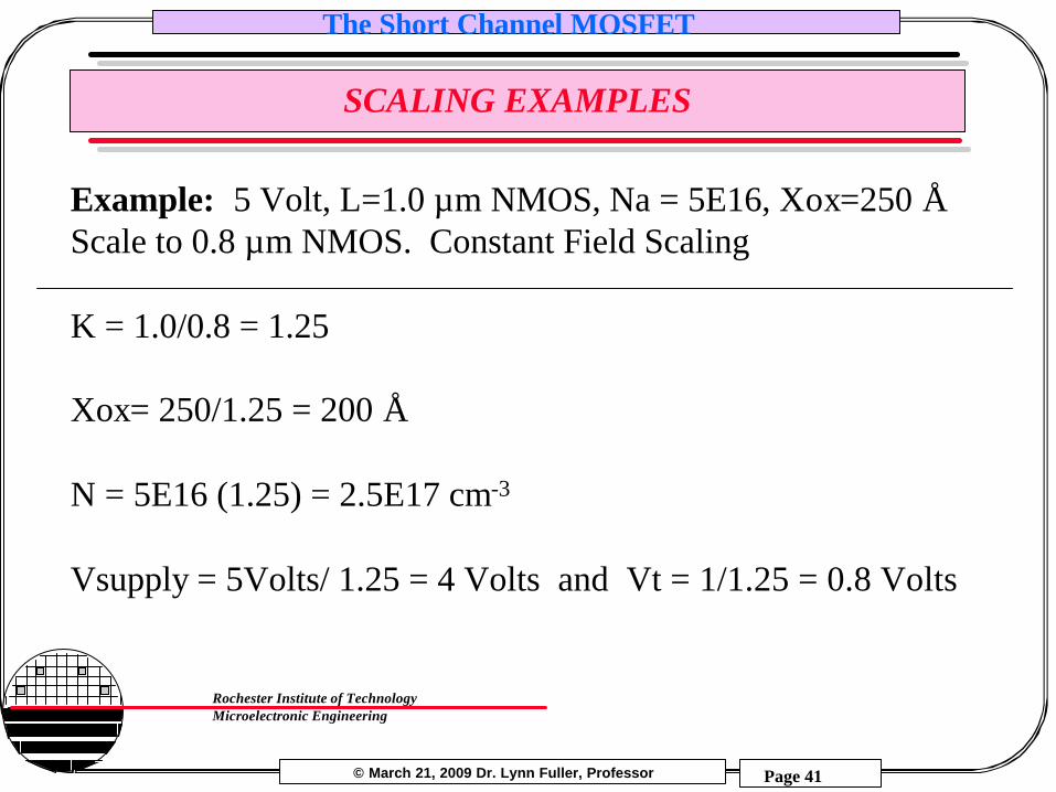
SCALING EXAMPLES
Example: 5 Volt, L=1.0 µm NMOS, Na = 5E16, Xox=250 ÅScale to 0.8 µm NMOS. Constant Field Scaling
K = 1.0/0.8 = 1.25
Xox= 250/1.25 = 200 Å
N = 5E16 (1.25) = 2.5E17 cm-3
Vsupply = 5Volts/ 1.25 = 4 Volts and Vt = 1/1.25 = 0.8 Volts
© March 21, 2009 Dr. Lynn Fuller, Professor
Rochester Institute of TechnologyMicroelectronic Engineering
The Short Channel MOSFET
Page 42
GATE OXIDE THICKNESS
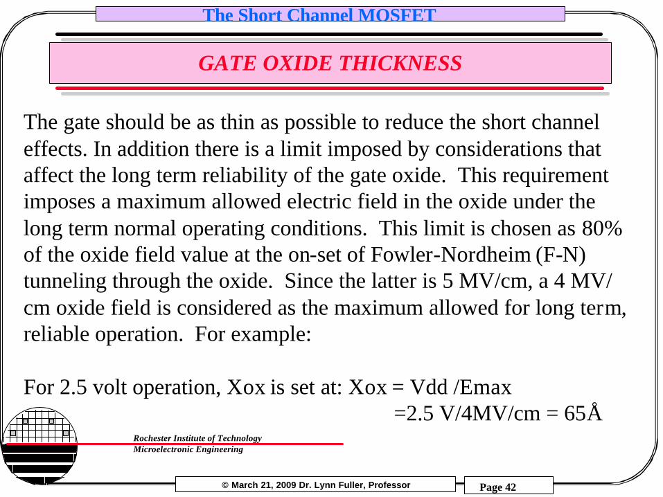
The gate should be as thin as possible to reduce the short channel effects. In addition there is a limit imposed by considerations that affect the long term reliability of the gate oxide. This requirement imposes a maximum allowed electric field in the oxide under the long term normal operating conditions. This limit is chosen as 80% of the oxide field value at the on-set of Fowler-Nordheim (F-N) tunneling through the oxide. Since the latter is 5 MV/cm, a 4 MV/ cm oxide field is considered as the maximum allowed for long term, reliable operation. For example:
For 2.5 volt operation, Xox is set at: Xox = Vdd /Emax=2.5 V/4MV/cm = 65Å
© March 21, 2009 Dr. Lynn Fuller, Professor
Rochester Institute of TechnologyMicroelectronic Engineering
The Short Channel MOSFET
Page 43
SALICIDE
Ti Salicide will reduce the sheet resistance of the poly and the drain and source regions. Salicide is an acronym for Self Aligned Silicide and Silicide is a material that is a combination of silicon and metal such as Ti, W or Co. These materials are formed by depositing a thin film of the metal on the wafer and then heating to form a Silicide. The Silicide forms only where the metal is in contact with the Silicon or poly. Etchants can remove the metaland leave the Silicide thus the term Self Aligned Silicide or SALICIDE.
© March 21, 2009 Dr. Lynn Fuller, Professor
Rochester Institute of TechnologyMicroelectronic Engineering
The Short Channel MOSFET
Page 44
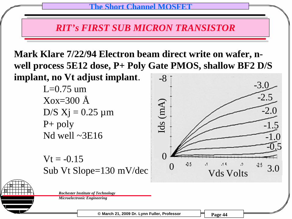
RIT’s FIRST SUB MICRON TRANSISTOR
Mark Klare 7/22/94 Electron beam direct write on wafer, n-well process 5E12 dose, P+ Poly Gate PMOS, shallow BF2 D/S implant, no Vt adjust implant.
L=0.75 umXox=300 ÅD/S Xj = 0.25 µmP+ polyNd well ~3E16
Vt = -0.15Sub Vt Slope=130 mV/dec
-3.0-2.5-2.0-1.5-1.0-0.5
0 3.0Vds VoltsId
s (m
A)
0
-8
© March 21, 2009 Dr. Lynn Fuller, Professor
Rochester Institute of TechnologyMicroelectronic Engineering
The Short Channel MOSFET
Page 45
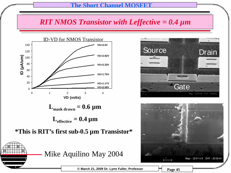
RIT NMOS Transistor with Leffective = 0.4 µm
0
20
40
60
80
100
120
140
0 1 2 3 4
VD (volts)
ID (
µA/u
m)
VG=3.5V
VG=2.92V
VG=2.33V
VG=1.75V
VG=1.17V
VG=0.58V
Lmask drawn = 0.6 µm
Leffective = 0.4 µm
*This is RIT’s first sub-0.5 µm Transistor*
Gate
Source Drain
ID-VD for NMOS Transistor
Mike Aquilino May 2004
© March 21, 2009 Dr. Lynn Fuller, Professor
Rochester Institute of TechnologyMicroelectronic Engineering
The Short Channel MOSFET
Page 46
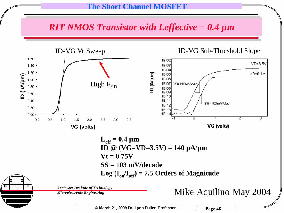
RIT NMOS Transistor with Leffective = 0.4 µm
0.00
0.20
0.40
0.60
0.80
1.00
1.20
1.40
1.60
0.0 0.5 1.0 1.5 2.0 2.5 3.0 3.5
VG (volts)
ID (
µA/µ
m)
ID-VG Sub-Threshold SlopeID-VG Vt Sweep
High RSD
Leff = 0.4 µmID @ (VG=VD=3.5V) = 140 µA/µmVt = 0.75VSS = 103 mV/decadeLog (Ion/Ioff) = 7.5 Orders of Magnitude
Mike Aquilino May 2004
© March 21, 2009 Dr. Lynn Fuller, Professor
Rochester Institute of TechnologyMicroelectronic Engineering
The Short Channel MOSFET
Page 47
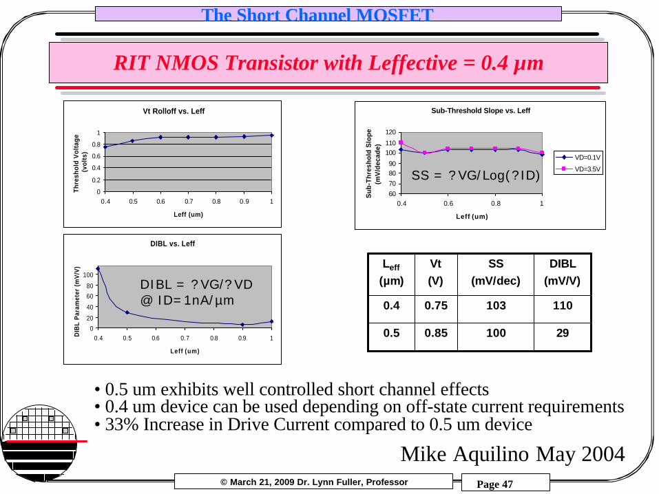
RIT NMOS Transistor with Leffective = 0.4 µm
Vt Rolloff vs. Leff
0
0.2
0.4
0.6
0.8
1
0.4 0.5 0.6 0.7 0.8 0.9 1
Leff (um)
Thre
shol
d V
olta
ge
(vo
lts)
Sub-Threshold Slope vs. Leff
60708090
100110
120
0.4 0.6 0.8 1
Leff (um)
Su
b-T
hre
sho
ld S
lop
e (m
V/d
ecad
e)
VD=0.1V
VD=3.5V
DIBL vs. Leff
0
20
40
60
80
100
0.4 0.5 0.6 0.7 0.8 0.9 1
Leff (um)
DIB
L P
aram
eter
(m
V/V
)
DIBL = ? VG/? VD@ ID=1nA/µm
SS = ? VG/Log(?ID)
291000.850.5
1101030.750.4
DIBL (mV/V)
SS (mV/dec)
Vt(V)
Leff
(µm)
• 0.5 um exhibits well controlled short channel effects• 0.4 um device can be used depending on off-state current requirements• 33% Increase in Drive Current compared to 0.5 um device
Mike Aquilino May 2004
© March 21, 2009 Dr. Lynn Fuller, Professor
Rochester Institute of TechnologyMicroelectronic Engineering
The Short Channel MOSFET
Page 48
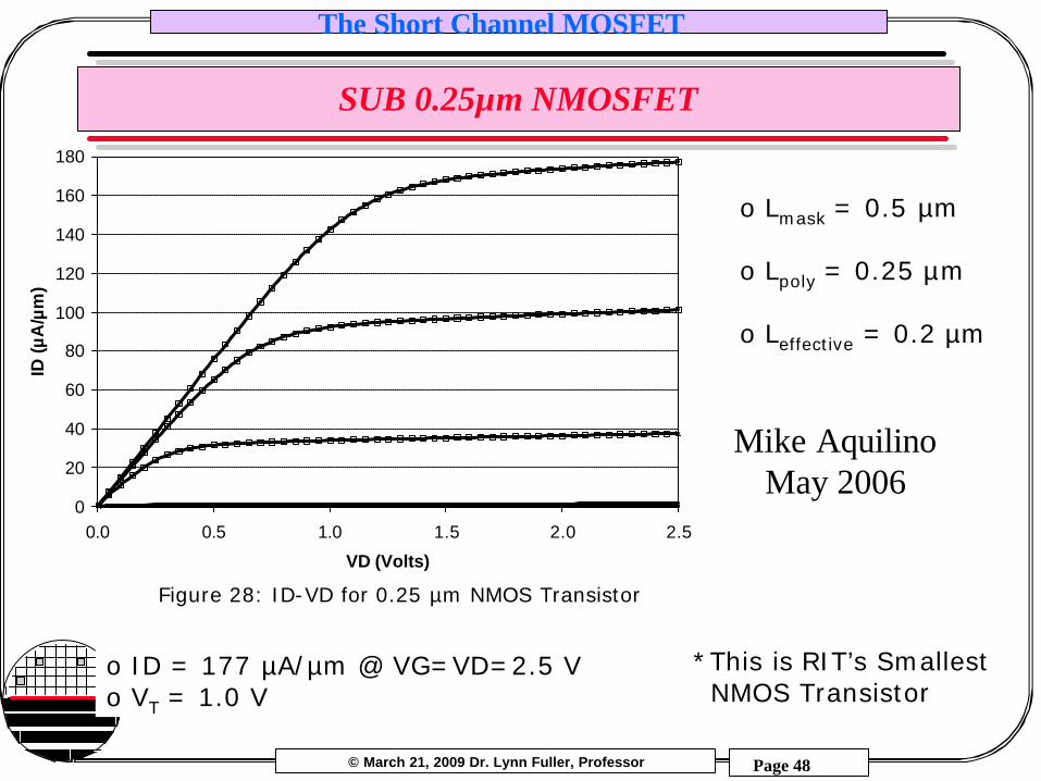
SUB 0.25µm NMOSFET
o ID = 177 µA/µm @ VG=VD=2.5 Vo VT = 1.0 V
o Lmask = 0.5 µm
o Lpoly = 0.25 µm
o Leffective = 0.2 µm
Figure 28: ID-VD for 0.25 µm NMOS Transistor
*This is RIT’s SmallestNMOS Transistor
0
20
40
60
80
100
120
140
160
180
0.0 0.5 1.0 1.5 2.0 2.5
VD (Volts)
ID (
µA
/µm
)
Mike AquilinoMay 2006
© March 21, 2009 Dr. Lynn Fuller, Professor
Rochester Institute of TechnologyMicroelectronic Engineering
The Short Channel MOSFET
Page 49
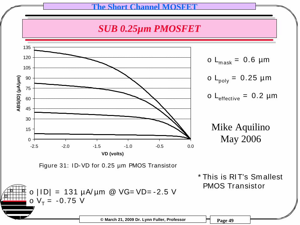
SUB 0.25µm PMOSFET
o Lmask = 0.6 µm
o Lpoly = 0.25 µm
o Leffective = 0.2 µm
o |ID| = 131 µA/µm @ VG=VD=-2.5 Vo VT = -0.75 V
Figure 31: ID-VD for 0.25 µm PMOS Transistor
*This is RIT’s SmallestPMOS Transistor
0
15
30
45
60
75
90
105
120
135
-2.5 -2.0 -1.5 -1.0 -0.5 0.0
VD (volts)
AB
S(I
D)
(µA
/µm
)
Mike AquilinoMay 2006
© March 21, 2009 Dr. Lynn Fuller, Professor
Rochester Institute of TechnologyMicroelectronic Engineering
The Short Channel MOSFET
Page 50
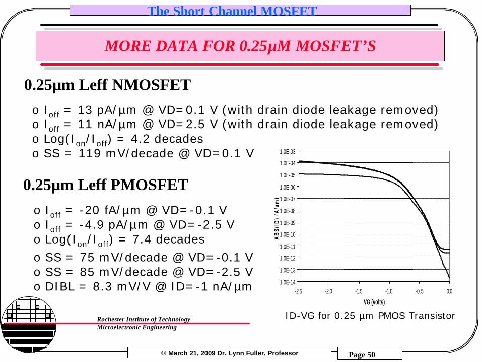
MORE DATA FOR 0.25µM MOSFET’S
o Ioff = -20 fA/µm @ VD=-0.1 Vo Ioff = -4.9 pA/µm @ VD=-2.5 Vo Log(Ion/Ioff) = 7.4 decadeso SS = 75 mV/decade @ VD=-0.1 Vo SS = 85 mV/decade @ VD=-2.5 Vo DIBL = 8.3 mV/V @ ID=-1 nA/µm
o Ioff = 13 pA/µm @ VD=0.1 V (with drain diode leakage removed)o Ioff = 11 nA/µm @ VD=2.5 V (with drain diode leakage removed)o Log(Ion/Ioff) = 4.2 decadeso SS = 119 mV/decade @ VD=0.1 V
0.25µm Leff NMOSFET
0.25µm Leff PMOSFET
1.0E-14
1.0E-13
1.0E-12
1.0E-11
1.0E-10
1.0E-09
1.0E-08
1.0E-07
1.0E-06
1.0E-05
1.0E-04
1.0E-03
-2.5 -2.0 -1.5 -1.0 -0.5 0.0
VG (volts)
AB
S(ID
) (A
/µm
)
ID-VG for 0.25 µm PMOS Transistor
© March 21, 2009 Dr. Lynn Fuller, Professor
Rochester Institute of TechnologyMicroelectronic Engineering
The Short Channel MOSFET
Page 51
REFERENCES
1. Device Electronics for Integrated Circuits, Richard S. Muller, Theodore I. Kamins, John Wiley & Sons., 1977.
2. Silicon Processing for the VLSI Era, Vol. 2&3., Stanley Wolf, Lattice Press, 1995.
3. The Science and Engineering of Microelectronic Fabrication, Stephen A. Campbell, Oxford University Press, 1996.
4. The MOS Transistor, Yannis Tsividis, 2nd Edition, McGraw Hill, 1999
© March 21, 2009 Dr. Lynn Fuller, Professor
Rochester Institute of TechnologyMicroelectronic Engineering
The Short Channel MOSFET
Page 52
HOMEWORK – SHORT CHANNEL MOSFETs
1. In short channel devices the threshold voltage becomes less than expected for long channel devices. Why.2. Explain reverse short channel effect.3. What is the effect of narrow channel width on transistor device characteristics.4. What is the purpose of low doped drain structures?5. How does mobility degradation and velocity saturation effect transistor device characteristics?6. Why is P+ doped poly used for PMOS transistors.7. What is the difference between mask channel length and effective channel length.8. What is punchthrough? What processing changes can be made to compensate for punchthrough?9. When scaling from 2 um to 1.5 um give new values for: device dimensions W,L,Xox, doping concentration, bias voltages, bias currents, power dissipation, transit time. 10. What is SALICIDE process. Why is it used?