the study of structural, morphological and optical
TRANSCRIPT

This is a repository copy of The study of structural, morphological and optical properties of(Al, Ga)-doped ZnO: DFT and experimental approaches.
White Rose Research Online URL for this paper:http://eprints.whiterose.ac.uk/143993/
Version: Accepted Version
Article:
Sikam, P, Moontragoon, P, Ikonic, Z et al. (2 more authors) (2019) The study of structural, morphological and optical properties of (Al, Ga)-doped ZnO: DFT and experimental approaches. Applied Surface Science, 480. pp. 621-635. ISSN 0169-4332
https://doi.org/10.1016/j.apsusc.2019.02.255
© 2019 Elsevier B.V. All rights reserved. Licensed under the Creative Commons Attribution-Non Commercial No Derivatives 4.0 International License (https://creativecommons.org/licenses/by-nc-nd/4.0/).
[email protected]://eprints.whiterose.ac.uk/
Reuse
This article is distributed under the terms of the Creative Commons Attribution-NonCommercial-NoDerivs (CC BY-NC-ND) licence. This licence only allows you to download this work and share it with others as long as you credit the authors, but you can’t change the article in any way or use it commercially. More information and the full terms of the licence here: https://creativecommons.org/licenses/
Takedown
If you consider content in White Rose Research Online to be in breach of UK law, please notify us by emailing [email protected] including the URL of the record and the reason for the withdrawal request.
1
The study of structural, morphological and optical properties of (Al, Ga)-doped ZnO:
DFT and experimental approaches
Pornsawan Sikam1, Pairot Moontragoon1,2,3*, Zoran Ikonic4, Thanayut Kaewmaraya1,2 ,
Prasit Thongbai1,2
1Department of Physics, Khon Kaen University, Khon Kaen, 40002, Thailand. 2Integrated Nanotechnology Research Center (INRC), Department of Physics, Khon Kaen
University, Khon Kaen, 40002, Thailand. 3Thailand Center of Excellence in Physics, Commission on Higher Education, Bangkok,
10400, Thailand. 4School of Electronic and Electrical Engineering, University of Leeds, Woodhouse Lane,
Leeds LS2 9JT, United Kingdom.
*Corresponding author at: Department of Physics, Faculty of Science, Khon Kaen University,
Khon Kaen, 40002, Thailand.
Tel.: +66 87 5149482; fax: +66 43 202374.
E-mail addresses [email protected] (P. Moontragoon)
2
ABSTRACT
ZnO is widely studied for several applications such as a photocatalyst, a working
electrode for dye-sensitized solar cells and for thermoelectric devices. This work studies the
effect of an increase in the number of carriers by doping ZnO with Al and Ga. The 6.25 mol%
of Al-doped ZnO, 6.25 mol% of Ga-doped ZnO, and 12.5 mol% of (Al, Ga) co-doped ZnO
nanoparticles were prepared using combustion method. The prepared samples were then
characterized by X-ray diffraction, transmission electron microscope, energy-dispersive X-ray
spectroscopy and UV-visible spectroscopy techniques. Moreover, density functional theory
(DFT) was also employed for computational studies of Al and Ga doped ZnO. Optimized
structures, density of states (DOS) and band structures of these materials were calculated using
Vienna Ab initio Simulation Package code. From this study, Al and Ga are found to play an
important role in morphology and optical properties of the ZnO, changing the band gap and
Fermi level of ZnO. Then, the prepared samples were characterised for their thermoelectric
properties, and modelling of thermoelectric properties of ZnO, Al-doped ZnO, Ga-doped ZnO
and (Al, Ga)-co doped ZnO was performed using BoltzTraP code. Furthermore, the Seebeck
coefficient, electrical conductivity, relaxation time, electronic thermal conductivity and power
factor were studied. The experimental and computational results are pointing in the same
direction, that the thermoelectric properties of the ZnO are changed by doping: the
semiconducting ZnO transforms into metallic ZnO when doped with Al and Ga. This leads to
ZnO showing new thermoelectric properties, in particular the Ga-doped ZnO and (Al, Ga)-co
doped ZnO: they provide high electrical conductivity and power factor. Therefore, it is
expected that these good properties might promote the ZnO to be a potential candidate for
applications, especially in high efficiency thermoelectric devices.
Keywords: Thermoelectric properties, DFT, Al -doped ZnO, Ga-doped ZnO, (Al-Ga)-co
doped ZnO
3
1. Introduction
ZnO is a semiconductor which is cheap to synthesize using various methods such as
hydrothermal [1], combustion [2], microemulsion [3] and sol-gel [4]. Because of the very
simple routes to prepare the ZnO, there are a number of research efforts trying to apply it in
various applications: solar cells [5], photocatalysts for degradation reaction [6, 7], transistors
[8] and gas sensors [9]. In addition, in the last two decades the ZnO has attracted attention for
its prospects to be used in thermoelectric devices [10-14]. An advantage of ZnO thermoelectric
devices is that semiconductors are commonly known from theory to provide a larger Seebeck
coefficient than metals. However, semiconductors have smaller electrical conductivity than
metals. Thus, ZnO is a potential candidate for efficient thermoelectric devices. There is an
exploration route to improve thermoelectric properties of ZnO by doping it with other atoms,
so that one could engineer the band structure and improve thermoelectric properties of the host
materials [2, 14, 15].
Briefly about the thermoelectric properties, the dimensionless figure of merit ZT is defined
to be a thermoelectric performance indicator, where ZT = (S2jT)/せ and S is the Seebeck
coefficient, giving the voltage difference between two points per unit temperature difference,
j is the electrical conductivity, T the temperature and せ the thermal conductivity, where せ = せe
+ せl where せe is the electronic thermal conductivity and せl is the lattice thermal conductivity or
phonon thermal conductivity [11, 13].
In 1997, Tsubota et al. [11] reported that the power factor at 1000 oC of the ZnO is about
4×10⁻⁴ Wm-1K-2 which is less than that of Zn0.95Al 0.05O; it is about 13×10-4 Wm-1K-2. Here, it
is interesting to note that Al doping increases the power factor at higher temperature, compared
to the pure ZnO. In the same direction as in the report of Ohtaki et al. [12], the ZT of
Zn0.98Al0.02O of around 0.2 was observed. However, there is an observed disadvantage:Tsubota
et al. [11] foundd that there is decrease in magnitude of the Seebeck coefficient when Al is
added into the ZnO structure. Moreover, an increase in electrical conductivity and the decrease
in magnitude of the Seeback coefficient when Al atoms were added into the ZnO are also shown
by Qu et al. [10] and Jantrasee et al. [13]. In addition to Al doping, Ga is also used for doping
ZnO. Khuili et al. [16] gave a computational result in 2016 that electrical conductivity of the
Al -doped ZnO and Ga-doped ZnO shows larger values than that of the pure ZnO.
From this point, it is realized that adding other atoms into the host ZnO structure, especially
Al and Ga, might enhance the thermoelectric performance of ZnO because introducing Al and
Ga in ZnO increases the carriers density in the system, which is expected to increase electrical
conductivity, because of electrons added in the ZnO. A following interesting question is on

4
how the thermoelectric properties of ZnO will be affected if the Al and Ga atoms are together
doped into the ZnO; that is, co-doping of Al and Ga in ZnO. Thus, this work studies the effects
of the Al and Ga doping on the structural, optical and thermoelectric properties of the ZnO host
structure via experimental and first-principles calculation approaches. In the experiment,
combustion method is chosen to synthesize the ZnO, Al-doped ZnO, Ga-doped ZnO and (Al,
Ga)-doped ZnO because this synthesis is very simple and faster than other methods. Moreover,
the density functional theory (DFT) study with generalized gradient approximation (GGA) is
employed for computational study.
2. Experimental details
2.1 Synthesis details
The ZnO, Zn1-xAl xO, Zn1-xGaxO and Zn1-2xAl xGaxO (x = 0.0625) nanoparticles were
synthesized using a combustion method. Firstly, Zn(CH3CO2)2 was dissolved in deionized (DI)
water. Next, AlN3O9.9H2O solution was added into the ZnO solution with continuous stirring
for the preparation of Zn1-xAl xO. After that, dissolved citric acid in ethanol and dissolved
polyethylene glycol (PEG) in ethanol were mixed into the previous solution while being stirred
continually. Then, the final solution was continuously stirred and heated at 220 °C. After the
solution transform to gel, it was heated into an oven at 350 °C for an hour, combustion process.
After cooling down, as-synthesized powder will be obtained. The next step is that the precursor
would be calcined at 500 °C in normal atmosphere for 8-hours with heating rate 1 oC/minute.
In case of Zn1-xGaxO, GaN3O9.xH2O solution would be added instead of the AlN3O9.9H2O
solution and, both GaN3O9.xH2O and AlN3O9.9H2O were added for the
Zn1-2xAl xGaxO.
2.2 Characterizations
Having calcined, the produced powders were characterized for their structure and
examined for composition elements using X-ray diffraction technique (XRD, PANalytical,
EMPYREAN) and energy-dispersive X-ray spectroscopy analysis (EDX, SEC, SNE-4500M),
respectively. Then, the transmission electron microscopy (TEM) photographs and selected area
electron diffraction (SAED) were studied via the transmission electron microscopy (FEI,
TECNAI G2 20). Additionally, the optical band gap of prepared samples was examined by
using UV-Vis spectroscopy (Shimadzu, UV-3101PC) in absorbance mode under ultraviolet
and visible spectra radiation. Finally, synthesized powder was hot pressed and polished as bulk.
Then, the Seebeck coefficient and electrical conductivity of prepared samples were found using
TRC-ZTM2.

5
3. Computational details
First of all, a 222 supercell of ZnO was used as initial model. This system contains
32 atoms, i.e. sixteen zinc atoms and sixteen oxygen atoms. In case of density of states (DOS),
band structure and phonon calculation, Vienna Ab initio Simulation Package (VASP) [17] with
Projector-augmented plane wave pseudopotential method (PAW) [18] were employed under
the generalized gradient approximation (GGA) of the scheme of Perdew–Burke–Ernzerh
(PBE) to treat exchange and correlation energy. In this calculation, 400 eV cutoff energy for
plane waves was used, and the orbitals of Zn(d10 p2) and O(s2 p4) were treated as valence
electrons. After that, a Zn atom was replaced by Al and Ga atoms for Al-doped ZnO and Ga-
doped ZnO, respectively. Moreover, two atoms of Zn were substituted by one atom of Al and
one atom of Ga for (Al,Ga)-co doped ZnO. For Al and Ga, electrons in Al(s2p1) and Ga(s2p1)
orbitals were treated as valence electrons. 553 k-point meshes in the Brillouin zone were
employed in optimization while 13137 of k-point grids were utilized to calculate DOS and
band structures. The study of thermoelectric properties, 212121 of k-point grids were used
for the calculation of thermoelectric properties under the semi-classical Boltzmann transport
theory in BoltzTraP [10, 19-21].
4. Results and discussion
In the first step, total energy of Al and Ga substitution on Zn and O sites is calculated
to examine which host atoms these doping atoms could replace. The calculated total energy of
Al and Ga doping on the ZnO structure is presented in Table 1. Here, the substitution of Al and
Ga atoms on the Zn sites shows a smaller total energy, compared to the O sites. This shows
that the added Al and Ga might replace the Zn sites. Therefore, this work will study the pure
ZnO and Zn-site substitution by Al and Ga named as undoped ZnO, Zn1-xAl xO, Zn1-xGaxO and
Zn1-2xAl xGaxO (x = 0.0625).
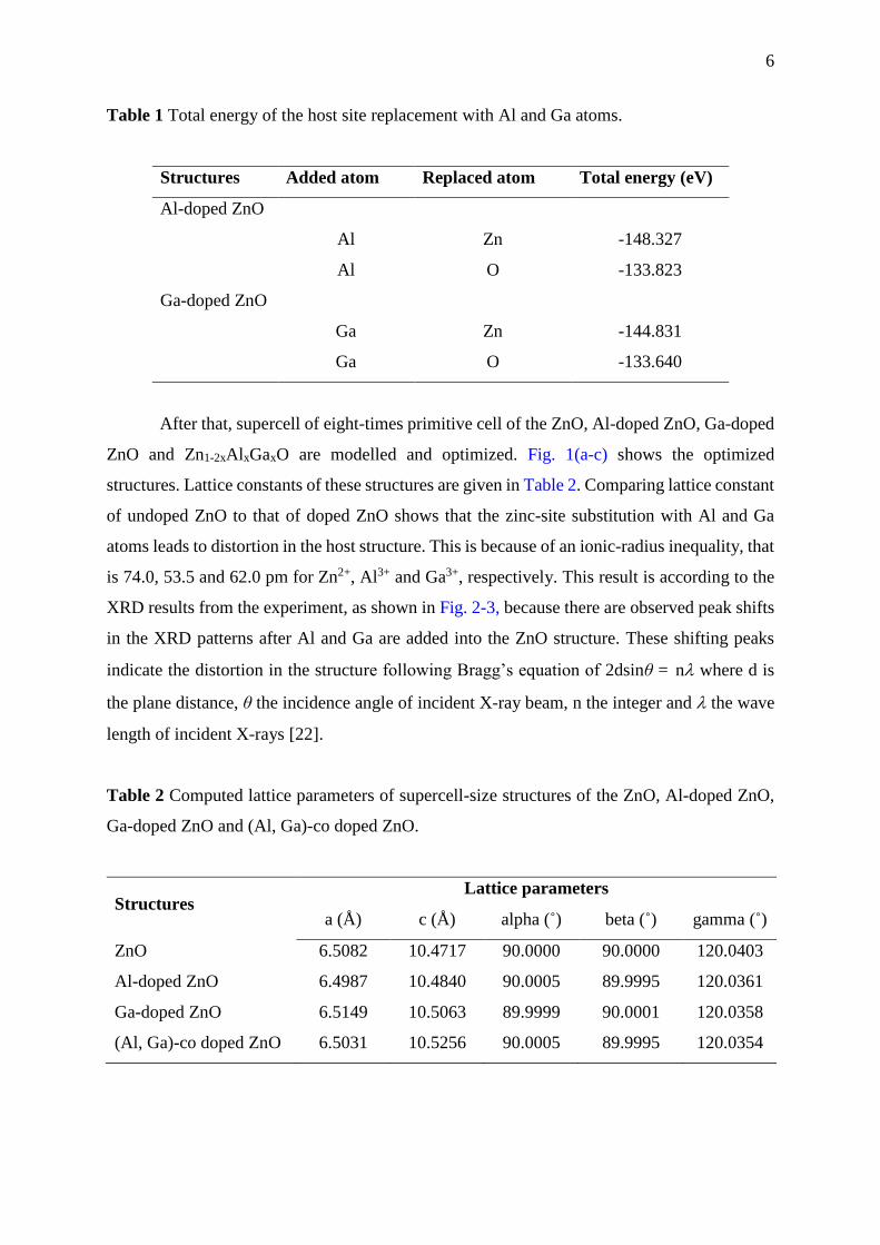
6
Table 1 Total energy of the host site replacement with Al and Ga atoms.
Structures Added atom Replaced atom Total energy (eV)
Al-doped ZnO
Al Zn -148.327
Al O -133.823
Ga-doped ZnO
Ga Zn -144.831
Ga O -133.640
After that, supercell of eight-times primitive cell of the ZnO, Al -doped ZnO, Ga-doped
ZnO and Zn1-2xAl xGaxO are modelled and optimized. Fig. 1(a-c) shows the optimized
structures. Lattice constants of these structures are given in Table 2. Comparing lattice constant
of undoped ZnO to that of doped ZnO shows that the zinc-site substitution with Al and Ga
atoms leads to distortion in the host structure. This is because of an ionic-radius inequality, that
is 74.0, 53.5 and 62.0 pm for Zn2+, Al3+ and Ga3+, respectively. This result is according to the
XRD results from the experiment, as shown in Fig. 2-3, because there are observed peak shifts
in the XRD patterns after Al and Ga are added into the ZnO structure. These shifting peaks
indicate the distortion in the structure following Bragg’s equation of 2dsinし = n where d is
the plane distance, し the incidence angle of incident X-ray beam, n the integer and the wave
length of incident X-rays [22].
Table 2 Computed lattice parameters of supercell-size structures of the ZnO, Al-doped ZnO,
Ga-doped ZnO and (Al, Ga)-co doped ZnO.
Structures Lattice parameters
a (Å) c (Å) alpha (̊) beta (̊) gamma (̊)
ZnO 6.5082 10.4717 90.0000 90.0000 120.0403
Al -doped ZnO 6.4987 10.4840 90.0005 89.9995 120.0361
Ga-doped ZnO 6.5149 10.5063 89.9999 90.0001 120.0358
(Al, Ga)-co doped ZnO 6.5031 10.5256 90.0005 89.9995 120.0354

7
Overall, the ZnO, Al -doped ZnO, Ga-doped ZnO and (Al, Ga)-co doped ZnO were
successfully synthesized using the combustion method in the experimental part. All prepared
samples show hexagonal wurtzite structure of ZnO (ICDD: 36-1451) as the main phase, as seen
in Fig. 2. Comparing the as-prepared and calcined samples, calcination makes the observed
peaks sharper. That is, the heat treatment leads to more regular atomic arrangement.
Nonetheless, an existence of the added Al and Ga contents is confirmed by the EDX analysis,
as shown in Fig. 4. The presented data is an elemental composition as a relative percentage.
In addition to success in the doping Al and Ga on the ZnO structure, nanoparticles are
obtained as well, as seen in Fig. 5. From the TEM images it follows that particle size changes,
from an average size around 80-100 nm to 20-40 nm, by the added Al and Ga contents. The
smaller particle size and shape edge might be caused by the reduced structural formation,
compared to the updoped ZnO. This is because the added atoms might inhibit the wurtzite
structural formation of Zn and O, leading to some defects in the structures, and decrease the
particle size. Moreover, the crystal planes of the ZnO wurtzite structure are observed in all
prepared samples, as seen in SAED patterns in Fig. 5.
Moving to the calculation aspects, Fig. 6 shows the total DOS (TDOS) of the undoped
ZnO, Al-doped ZnO, Ga-doped ZnO and (Al, Ga)-co doped ZnO, computed using 13×13×7 k-
point grids. Comparing TDOS of the doped to the undoped ZnO, there is a shift of the valence
band maximum from 1.13 eV for the ZnO to 1.32 eV for the Ga-doped ZnO, 1.40 eV for the
co-doped system and 1.41 eV for the Al doping. This might affect the band gap and band edge
of the materials, and it also might affect their thermoelectric properties (TE). However, more
details concerning the optical properties will be discussed later. In addition, upwards shift of
the Fermi level (Ef) is also observed. In the ZnO, the Ef is positioned at the highest states of
valence band, while in the doped system the Ef locates in the conduction band, according to the
report of Jantrasee et al. and Khuili et al. [13, 16]. This point indicates that adding Al and Ga
atoms in the ZnO structure leads to shift of Fermi level upwards, because the Zn2+ site
substitution with Al3+ and Ga3+ is the n-type doping; i.e. more free electrons will be generated
from donor states, resulting in the shifting of the Ef state to higher level (in the conduction
band). This point is important because the Fermi level affects the TE properties [14].
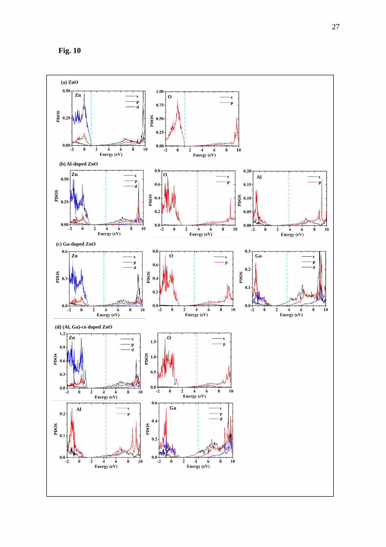
Partial DOS and projected DOS, as shown in Fig. 6-10, will be considered next. For the
undoped ZnO, the maximum state is occupied by Zn and O carriers, d-orbital electrons of Zn
and p-orbital electrons of O, according to the report of Hachimi et al. [23]. After that, when Al
and Ga atoms are added into the ZnO structure, there are new states observed above the 1.13
eV, as previously seen in the total DOS. From the Fig. 10, the interaction in the highest states

8
of doped systems results from d-orbital for Zn, o-orbital for O, p-orbital for Al and d-orbital
for Ga. Moreover, comparing the projected DOS graphs of Zn and O in the doped systems to
that for the undoped system, the Zn and O show different DOS, especially in the top of valence
band. Therefore, it could be claimed that new states in the top of valence band come from
interaction of Al and Ga with the nearest neighbor atom, Zn and O. Here, it is seen that adding
Al and Ga on the ZnO could engineer DOS of the ZnO, which might lead to appreciating its
optical and TE properties. This result is according to the report of Khuili et al. [16].
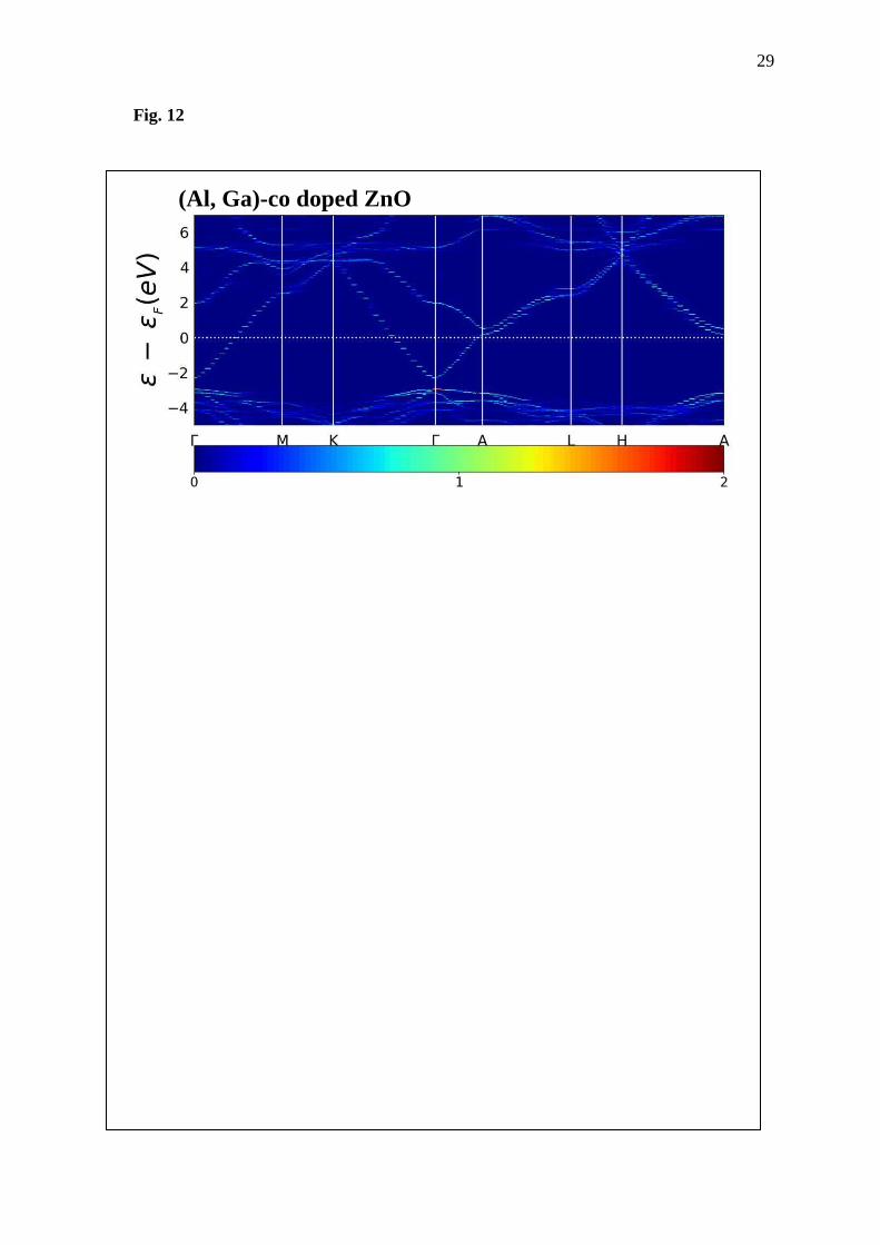
Another evidence presenting the difference of the ZnO and doped ZnO is their band
structure. Here, the band-up structures of supercell models are computed using band-up code
[24, 25] and shown in Fig. 11-12. Three-dimensional plots have the wave vector on the x axis,
the о-оF on the y axis and, the electron density on the z axis; represented by color from the
minimum value of blue (zero) to the maximum value of red. Here, ZnO shows direct band gap
because the maximum valence band and minimum conduction band are at the same d point, in
agreement with the literature, e.g. Honglin et al. and Mohamad et al. [26, 27]. Gap between
valence band and conduction band (Eg) is 0.76 eV. Moreover, there is light electron density at
the top of valence band. It is possible that electron hoping probability from the valence band to
the conduction band in pure ZnO may be smaller than in the doped ZnO. This is due to the fact
that all doped systems show heavy electron density on the top of valence band, almost twice as
large as the electron density. Additionally, not only the ZnO, but also all doped materials show
the direct band gap behavior. As for the band gap width, the Eg is 0.60, 0.53 and 0.64 eV for
the Al doping, Ga substitution and co-doped ZnO structures, respectively.
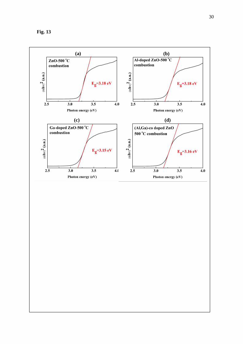
Then, the band gap of prepared samples will be discussed next. Graphs of photon
energy and (ghち)2 are illustrated in Fig. 13, where g is the absorption coefficient, h the Plank’s
constant and ち the photon frequency. This plot follows an equation of ghち = k(hち-Eg)n/2 when
k and n are constants, where n would be 1 and 4 for direct and indirect band gap materials,
respectively [28, 29]. From the results, ZnO shows the band gap of 3.18 eV while the Eg of the
doped systems is 3.18, 3.15 and 3.16 eV for Al-doped ZnO, Ga-doped ZnO and (Al, Ga)-co
doped ZnO, respectively. Comparing the DFT band structures to the optical band gap obtained
from the experiment, there is a considerable difference of obtained band gaps from these two
approaches. The large underestimate of the value of Eg obtained from the DFT study is caused
by unrealistic interaction force of electron-electron, electron-nucleus and nucleus-nucleus
interaction, due to limitations of the DFT calculation. However, the DFT is employed in this
work because less resources are required in calculation compared to Hartree-Fock
approximation. Although the obtained band gap from the first-principles calculation is not

9
equal to the experimental result, it can provide important evidences; this is what happens when
the Zn sites are replaced by Al and Ga atoms, such as partial DOS, projected DOS and
electronic band structures. However, an essential point of the band gap of these material is that
band gap of the doped ZnO is wider than that of the undoped ZnO. From this point, it is good
for the photocatalyst application of the ZnO because narrower band gap after Al and Ga adding
could support photocatalytic performance under the Sun radiation. Thus, it is possible that the
Al and Ga doping of the ZnO structure could organize the electron-occupied energy level and
band structure of the ZnO which might lead to the change in optical and thermoelectric
properties of the ZnO. Since electrons are fermions, the probability of occupying any energy
level is given by Fermi-Dirac distribution, the electron distribution will be a function of the Ef
and the Seebeck coefficient depends on both the Eg and Ef of semiconductor materials [30].
Thus, if there is change in both Ef and Eg when the Al and Ga were added into the ZnO, as
shown in the calculation results, it is possible that Al and Ga doping on the ZnO might improve
the TE properties of the ZnO.
Nevertheless, there is an option to correct the band gap in first-principles calculation.
This is by adding Hubbard parameter for d-orbital elements. The Hubbard parameter will be
added to adjust the interaction of d-orbital electrons. Here, the Hubbard parameter of Ueff as
9.0 eV (U=10.0 eV and J= 1.0 eV) and 7.0 eV is employed for Zn and Ga, respectively,
following the report of Jantrasee et al. [13] and Dong et al. [31]. In this work, the GGA+U
using k-point meshes of 21×21×21 for the ZnO and 13×13×7 for the doped systems will be
employed to calculate thermoelectric properties of undoped ZnO and doped ZnO because the
Fermi level of the doped systems is at conduction band already for 13×13×7 k-point grids.
DOS of these systems are calculated and shown in Fig 14-15. From the DOS, it is seen that the
Ef of the materials sits near the conduction band. The appearance of the Ef under the minimum
conduction band indicates that these materials should be n-type semiconductors due to majority
carriers being electrons, they generate donor states in the forbidden band, resulting in shift of
Ef from the middle gap for undoped semiconductors to the near conduction band for n-type
materials. The next step is to use the output data from these calculations for the thermoelectric
properties.

10
Thermoelectric properties calculated using BoltzTraP code for the ZnO and doped ZnO
are shown in Fig 16. From the graphs, the zinc oxide shows the negative value with magnitude
of Seebeck coefficient around 242 µV/K. This result is in accordance with the experimental
reports of Tsubota et al. and Qu et al. [10, 11]. Then, electronic thermal conductivity tends to
slightly increase with increasing temperature, corresponding to the reported results of Qu et al.
[10]. Comparing the doped ZnO to the pure ZnO, magnitude of the Seebeck coefficient of the
doped systems is obviously smaller than that of the pure ZnO, while electric conductivity per
relaxation time and electronic thermal conductivity per relaxation time of the doped ZnO are
higher than that of the pure ZnO. It is clear that Al and Ga doping of the ZnO could improve
electrical conductivity of the ZnO, according to the report of Khuili et al. and Qu et al. [10,
16].
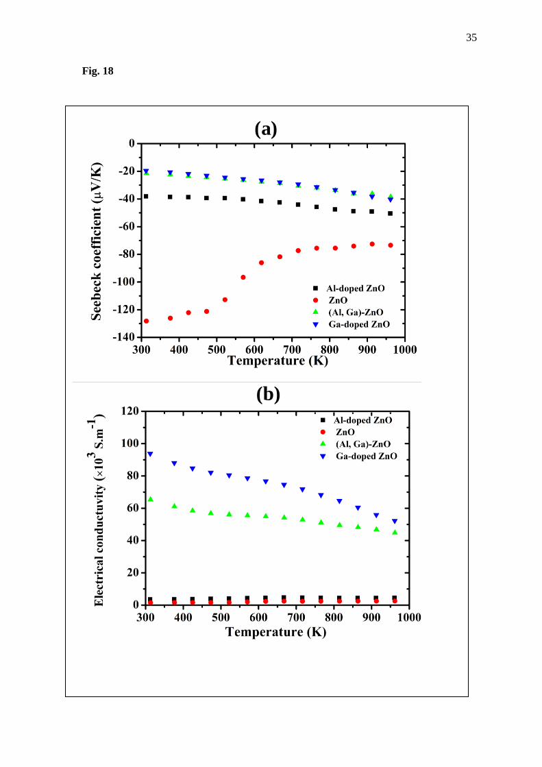
Moving to consider experimental parts, the plots of the thermoelectric properties of the
synthesized undoped ZnO and doped ZnO are shown in Fig. 17. The ZnO illustrates negative
value of the Seebeck coefficient with magnitude in range from about 70 to 128 たV/K.
Comparing the doped to the undoped ZnO, the decrease in magnitude of the Seebeck
coefficient of the ZnO with temperature increase is observed, while all the doped ZnO materials
show a larger magnitude with increasing temperature. Moreover, the doped ZnO shows
negative value of the Seebeck coefficient, similar to the undoped ZnO. However, the magnitude
of the Seebeck coefficient of the Al-doped ZnO is smaller than that of ZnO. From this point,
the observed experimental results are in accordance with the obtained computational results.
In case of the electrical conductivity j, the ZnO shows trend to increase with increasing
temperature, which is the same trend to the Al-doped ZnO; this trend is according to the
calculated result and report of the Qu et al. [10]. Nonetheless, the value of the electrical
conductivity of the Al-doped ZnO is a bit larger than that of the ZnO. For Ga-doped ZnO and
(Al, Ga)-doped ZnO, their electrical conductivity decreases with temperature increasing from
room temperature to 1000 K. However, it is still much larger than for the ZnO and Al-doped
ZnO. Both Ga-doped ZnO and (Al, Ga)-doped ZnO show a much appreciated electrical
conductivity because their electrical conductivity is very large compared to undoped ZnO and
Al -doped ZnO. From this result one can infer that Ga doping and cooperation of Al and Ga
could change semiconductor ZnO to be a metallic ZnO with high j.
Considering the electrical conductivity of the prepared samples and the calculation
result, obtained using BoltzTraP code (j/), it is assumed that at the same temperature, their
electrical conductivity would be the same. In this work, difference of the temperature of the

11
experiment and calculation is different up to 6.0 K. Therefore, electrical conductivity j of the
DFT calculation will be as shown in Fig. 18(up). After that, the relaxation time of materials
in Fig. 16 could be calculated using the electrical conductivity from Fig. 18(up). Then, the
relaxation time will be obtained as seen in Fig. 18(down). Here, it is seen that the ZnO shows
the largest value of the relaxation time. Their relaxation time is decreasing with temperature
increasing from 5.77 to 1.77×10⁻¹⁵ s for the temperature from 300 to 1000 K. This might be
because heating could lead carriers to have smaller relaxation time. This relaxation time is not
much smaller than that in the report of Ozgur et al., the reported 17×10-15 s for carrier
concentration of the order of 1016 cm-3 [32]. In case of doped ZnO, their relaxation time is much
smaller, compared to the ZnO. It might be due to their metallic behavior. This is because there
are more electrons there than in the undoped ZnO.
Next, the electronic thermal conductivity e will be obtained from the e/, using the
values of in Fig. 18(down). The obtained e are shown in Fig. 19(up). Additionally, the e is
calculated using Wiedemann-Franz law of e= LjT where L is the Lorenz factor (2.45×10⁻⁸
V2/K2), j the electrical conductivity and T the temperature [13, 33]. The j is in Fig. 18(up).
Here, the obtained e from two approaches almost equal. From the results, it is seen that ZnO
and Al-doped ZnO show very low electronic thermal conductivity while Ga doping and co
doping have the large e. Thus, Ga doping and (Al, Ga)-co doping on the ZnO could promote
both electrical and electronic conductivity of the ZnO because both properties come from
electron motion, conducting both electricity and heat.
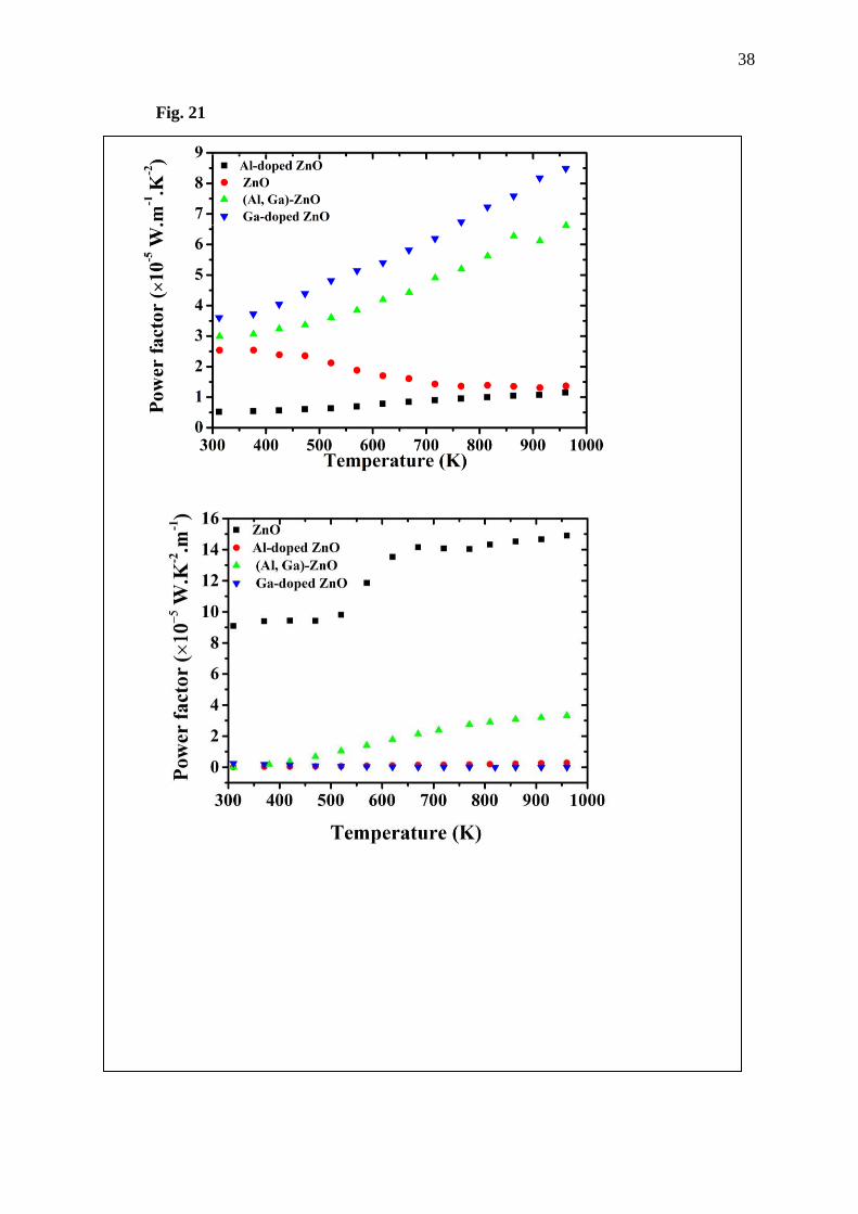
Finally, ability to transform heat to electrical energy of the prepared materials is studied
via power factor P , where P = S2j , where S is the Seebck coefficient and j the electrical
conductivity. Fig. 20(up) shows the graphs of power factor of the synthesized ZnO and doped
ZnO. Here, the power factor of the ZnO drops with temperature increase, which points out that
ability of ZnO to convert heat to electrical energy will decrease when it is used at higher
temperature. Nevertheless, an appreciated result is observed in the doped ZnO. The all doped
ZnO materials show greater power factor with temperature increase, especially Ga and (Al,
Ga)-co doped ZnO. This point is very interesting because it points out that Ga doping and (Al,
Ga)-co doping on the ZnO can improve the power factor of the ZnO and it gives much better
results than only Al-doped ZnO. In case of the Fig. 20(down), it is showing the power factor
obtained results from the DFT calculation. The massive power factor of the ZnO is observed.
This might be due to the fact that the Seebeck coefficient of the ZnO in Fig. 16 is very large
compared to the doped systems, about 10 times. Additionally, to calculate the power factor, the

12
Seebeck coefficient will be squared. Thus, the power factor of the ZnO should be about 100
times larger, compared to the doped ZnO. However, the possible reason that the power factor
of the ZnO is not 100 times larger than that of the doped ZnO is that electrical conductivity of
the doped ZnO is greater than the undoped ZnO. However, the difference of the calculation
and experimental results might come from the assumption that electrical conductivity of the
DFT calculation is equal to that of the experiment. Another reason is the temperature difference
of the calculation results and the experimental result as mentioned above. Moreover, the
employed parameters in calculations, such as Habbard parameter U and number of k-points,
might effect to the obtained results as well. Nonetheless, it cannot be denied that calculation
approach is still important because it can provide predictive guidelines and answer many
questions about experimental results.
From the thermoelectric properties obtained in this study of the undoped and doped
ZnO, it is possible that more electron carriers in the ZnO, when Al and Ga were added, results
in metallic behavior of the ZnO. The number of electron carriers is similar to Electron Sea,
leading to metallic behavior of the ZnO. Metals always show higher electrical conductivity
than the semiconductors, while the magnitude of Seebeck coefficient of the semiconductor is
greater than that of the metals. From this study, ZnO semiconductor, which shows large values
of Seebeck coefficient and very small electrical conductivity per relaxation time, transforms to
metallic ZnO, with smaller Seebeck coefficient, and with huge electrical conductivity and large
power factor, when Al and Ga were doped into the structure. This is due to the fact that the
Seebeck coefficient depends on the voltage difference of two points per temperature difference,
as mentioned above, and V=IR where V is the potential difference between two points, I the
current flowing through the resistance and R the resistance, obeying Ohm’s law. Thus, the
higher electrical conductivity is, the smaller is the Seebeck coefficient. This causes a decrease
of the Seebeck coefficient and ZT when Al and Ga are added into the ZnO. From this point, it
is clear that adding Al and Ga could change thermoelectric properties of the ZnO from the
semiconductor behavior to the metallic behavior with the very large electrical conductivity and
power factor.
5. Conclusions
In this work, structural, optical and thermoelectric properties of the ZnO, Al-doped
ZnO, Ga-doped ZnO and (Al, Ga)-co doped ZnO were studied via experimental and first-
principles calculation approaches. In experiment, nanoparticles of ZnO, Al-doped ZnO, Ga-
doped ZnO and (Al, Ga)-co doped ZnO are synthesized using combustion method. The results

13
from the XRD and SAED analysis confirm that main phase of the prepared samples is the
wurtzite structure without any secondary phases observed. Additionally, the DFT study with
GGA approximation is used via VASP code for calculating the supercells of these materials.
From the study, it is seen that the Al and Ga adding on the ZnO structures enables one to
engineer the ZnO’s band structure. There are new states at top of valence band which come
from interaction of valence electrons of Zn, O, Al and Ga atoms. The change in band structures
and DOS of the ZnO after Al and Ga are added into the structures indicates that the dopant
systems would show the impressive optical and thermoelectric properties. In this work, the
synthesized Ga-doped ZnO and (Al, Ga)-co doped ZnO materials could significantly improve
the thermoelectric properties of the ZnO, especially electrical conductivity and power factor.
Here, it is possible that they would be potential candidates to be thermoelectric materials for
high performance thermoelectric devices, because they could be synthesized using not very
complex routes, and they can provide a very high power factor. Additionally, another observed
benefit is that the calculated results agree well with experimental results. Therefore, great
properties observed in the calculated results of the ZnO and doped ZnO could be examined in
the real materials, not only in the simulation.
Acknowledgments
Funding for this work is provided by Thailand Research Fund under Grant No.
RTA5680008, Integrated Nanotechnology Research Center (INRC), Khon Kaen University,
Thailand, the Nanotechnology Center (NANOTEC), NSTDA, Ministry of Science and
Technology, Thailand, through its program of Center of Excellence Network, Science
Achievement Scholarship of Thailand (SAST).
References
1. Edalati, K., et al., Low-temperature hydrothermal synthesis of ZnO nanorods: Effects of zinc salt concentration, various solvents and alkaline mineralizers. Materials Research Bulletin, 2016. 74: p. 374-379.
2. Sikam, P., et al., Structural, Optical, Electronic and Magnetic Properties of Fe-Doped ZnO Nanoparticles Synthesized by Combustion Method and First-Principle Calculation. Journal of Superconductivity and Novel Magnetism, 2016. 29(12): p. 3155-3166.
3. Wang, Y., et al., Synthesis of ZnO nanoparticles from microemulsions in a flow type microreactor. Chemical Engineering Journal, 2014. 235: p. 191-197.
4. Hasnidawani, J.N., et al., Synthesis of ZnO Nanostructures Using Sol-Gel Method. Procedia Chemistry, 2016. 19: p. 211-216.

14
5. Huang, J., Z. Yin, and Q. Zheng, Applications of ZnO in organic and hybrid solar cells. Energy & Environmental Science, 2011. 4(10): p. 3861-3877.
6. Lee, K.M., et al., Recent developments of zinc oxide based photocatalyst in water treatment technology: A review. Water Research, 2016. 88: p. 428-448.
7. Chen, X., et al., Preparation of ZnO Photocatalyst for the Efficient and Rapid Photocatalytic Degradation of Azo Dyes. Nanoscale Research Letters, 2017. 12(1): p. 143.
8. Xu, X., et al., Low-voltage zinc oxide thin-film transistors with solution-processed channel and dielectric layers below 150竺°C. Applied Physics Letters, 2012. 101(22): p. 222114.
9. Biasotto, G., et al., Gas sensor applications of zinc oxide thin film grown by the polymeric precursor method. Ceramics International, 2014. 40(9, Part B): p. 14991-14996.
10. Qu, X., et al., Thermoelectric properties and electronic structure of Al-doped ZnO. Solid State Communications, 2011. 151(4): p. 332-336.
11. Tsubota, T., et al., Thermoelectric properties of Al-doped ZnO as a promising oxide material for high-temperature thermoelectric conversion. Journal of Materials Chemistry, 1997. 7(1): p. 85-90.
12. Ohtaki, M., et al., Highϋtemperature thermoelectric properties of (Zn1−xAlx)O. Journal of Applied Physics, 1996. 79(3): p. 1816-1818.
13. Jantrasee, S., S. Pinitsoontorn, and P. Moontragoon, First-Principles Study of the Electronic Structure and Thermoelectric Properties of Al-Doped ZnO. Journal of Electronic Materials, 2014. 43(6): p. 1689-1696.
14. Sikam, P., et al., Enhanced thermoelectric properties of N-doped ZnO and SrTiO3: A first-principles study. Applied Surface Science, 2018. 446: p. 47-58.
15. Sikam, P., et al., DFT calculation and experimental study on structural, optical and magnetic properties of Co-doped SrTiO3. Applied Surface Science, 2018. 446: p. 92-113.
16. Khuili, M., et al., Comparative first principles study of ZnO doped with group III elements. Journal of Alloys and Compounds, 2016. 688: p. 368-375.
17. Kresse, G. and J. Furthmüller, Efficiency of ab-initio total energy calculations for metals and semiconductors using a plane-wave basis set. Computational Materials Science, 1996. 6(1): p. 15-50.
18. Blöchl, P.E., Projector augmented-wave method. Physical Review B, 1994. 50(24): p. 17953-17979.
19. Madsen, G.K.H. and D.J. Singh, BoltzTraP. A code for calculating band-structure dependent quantities. Computer Physics Communications, 2006. 175(1): p. 67-71.
20. Jantrasee, S., P. Moontragoon, and S. Pinitsoontorn, Optical and magnetic properties of doped ZnO: Experi-mental and simulation. Journal of Optoelectronics and Advanced Materials, 2016. 18(11-12): p. 1033-1039.
21. Jantrasee, S., P. Moontragoon, and S. Pinitsoontorn, Thermoelectric properties of Al-doped ZnO: Experiment and simulation. Journal of Semiconductors, 2016. 37(9).
22. The reflection of X-rays by crystals. Proceedings of the Royal Society of London. Series A, 1913. 88(605): p. 428.
23. Hachimi, A.G.E., et al., First-principles prediction of the magnetism of 4f rare-earth-metal-doped wurtzite zinc oxide. Journal of Rare Earths, 2014. 32(8): p. 715-721.
24. Medeiros, P.V.C., S. Stafström, and J. Björk, Effects of extrinsic and intrinsic perturbations on the electronic structure of graphene: Retaining an effective primitive cell band structure by band unfolding. Physical Review B, 2014. 89(4): p. 041407.
15
25. Medeiros, P.V.C., et al., Unfolding spinor wave functions and expectation values of general operators: Introducing the unfolding-density operator. Physical Review B, 2015. 91(4): p. 041116.
26. Li, H., et al., First-principles study of p-type conductivity of N-Al/Ga/In co-doped ZnO. Physica Scripta, 2015. 90(2): p. 025803.
27. Mohamad, A.A., et al., First-principles calculation on electronic properties of zinc oxide by zinc–air system. Journal of King Saud University - Engineering Sciences, 2017. 29(3): p. 278-283.
28. Zhang, L., et al., Rapid synthesis of ultrafine K2Ln2Ti3O10 (Ln=La, Nd, Sm, Gd, Dy) series and its photoactivity. Journal of Solid State Chemistry, 2005. 178(3): p. 761-768.
29. Liu, C., et al., Influence of Fe-doping on the structural, optical and magnetic properties of ZnO nanoparticles. Journal of Magnetism and Magnetic Materials, 2012. 324(20): p. 3356-3360.
30. Azároff, L.V. and J.J. Brophy, Electronic processes in materials. 1963: McGraw-Hill. 31. Dong, L., et al., Effects of oxygen vacancies on the structural and optical properties
of く-Ga2O3. Scientific Reports, 2017. 7: p. 40160. 32. Özgür, Ü., et al., A comprehensive review of ZnO materials and devices. Journal of
Applied Physics, 2005. 98(4): p. 041301. 33. Scott, J.F., H.G. Bohn, and W. Schenk, Ionic Wiedemann–Franz law. Applied Physics
Letters, 2000. 77(16): p. 2599-2600.

16
LIST OF FIGURE CAPTIONS
Fig. 1 2×2×2 supercell of (a) ZnO, (b) Al-doped ZnO, (c) Ga-doped ZnO and (d) (Al, Ga)-co
doped ZnO where grey balls as the zinc atoms, red the oxygen, blue the aluminum and
green the gallium.
Fig. 2 XRD patterns of as-prepared and calcined samples.
Fig. 3 XRD patterns in range from 35.75 to 37.25 degree of 2theta of samples calcined at
500 oC.
Fig. 4 Elemental composition of (a) undoped ZnO, (b) Al-doped ZnO, (c) Ga-doped ZnO and
(d) (Al, Ga)-co doped ZnO calcined at 500 oC.
Fig. 5 (left) TEM images and (right) SAED patterns of undoped ZnO, Al-doped ZnO, Ga-
doped ZnO and (Al, Ga)-co doped ZnO calcined at 500 oC.
Fig. 6 Total DOS calculated using the GGA scheme of the PBE of (a) ZnO, (b) Al-doped ZnO,
(c) Ga-doped ZnO and (d) (Al, Ga)-co doped ZnO where Fermi level (Ef) is at 1.13,
3.82, 3.67 and 4.39 eV, respectively.
Fig. 7 Total and partial DOS calculated by the GGA approximation of the ZnO where the Ef
is at 1.13 eV, along dash line.
Fig. 8 Total and partial DOS of (a) Al-doped ZnO and (b) Ga-doped ZnO when the Ef is
addressed by dash line, locating at 3.82 and 3.67 eV for the Al-doped ZnO and Ga-
doped ZnO, respectively, computed by the DFT with GGA method.
Fig. 9 Obtained total and partial DOS from the calculation of DFT with GGA approach of (Al,
Ga)-co doped ZnO with the dash line of Ef at 4.39 eV
Fig. 10 Projected DOS calculated by the GGA approximation of (a) ZnO, (b) Al-doped ZnO,
(c) Ga-doped ZnO and (d) (Al, Ga)-co doped ZnO.
Fig. 11 Band structures, computed by the GGA scheme, of (a) ZnO, (b) Al-doped ZnO and (c)
Ga-doped ZnO.
Fig. 12 Band structure of (Al, Ga)-co doped ZnO obtained from the first-principles calculation
method with GGA approximation.
Fig. 13 Optical band gap of (a) ZnO, (b) Al-doped ZnO, (c) Ga-doped ZnO and (d) (Al, Ga)-
co doped ZnO: experimental results.
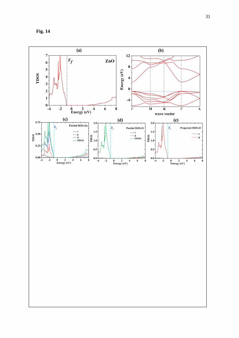
Fig. 14 DOS and band structure of primitive ZnO calculated using HSE calculation.
Fig. 15 DOS calculated using GGA+U approach of (a) 21×21×21 k-point meshes of ZnO and,
13×13×7 k-point meshes of (b) Al-doped ZnO, (c) Ga-doped ZnO and (d) (Al, Ga)-
17
doped ZnO where the Ef is at 1.96, 3.82, 3.63 and 4.37 eV for the ZnO, Al-doped ZnO,
Ga-doped ZnO and (Al, Ga)-co doped ZnO, respectively.
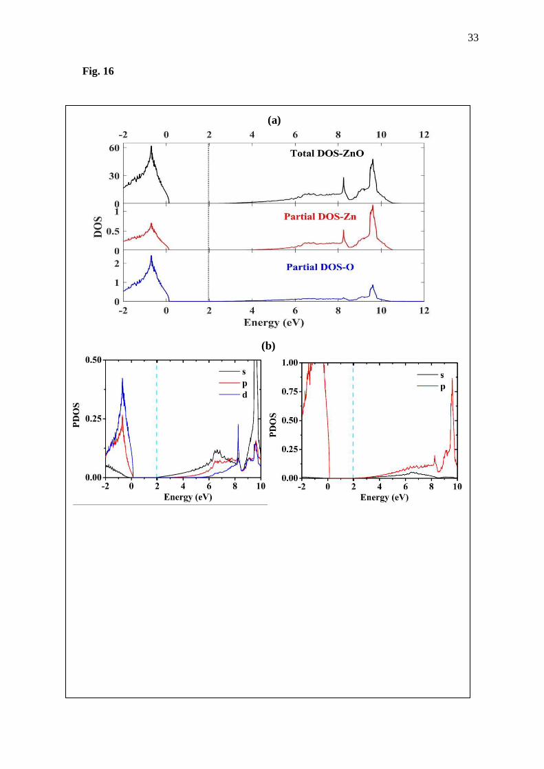
Fig. 16 (a) Total DOS and partial DOS and, (b) projected DOS of the (left) Zn and (right) O of
the ZnO computed using k-point meshes of 21×21×21 using GGA+U scheme.
Fig. 17 Thermoelectric properties calculated by BolzTraP code of (a) Seebeck coefficient, (b)
electrical conductivity divided by relaxation time and (c) electronic thermal
conductivity per relaxation time of ZnO, Al-doped ZnO, Ga-doped ZnO and (Al, Ga)-
co doped ZnO.
Fig. 18 Thermoelectric properties of (a) Seebeck coefficient and (b) electrical conductivity j
of prepared materials.
Fig. 19 (up) Electrical conductivity j and (down) relaxation time: calculation part.
Fig. 20 Electronic thermal conductivity obtained from (up) BoltzTraP code and (down)
Wiedemann-Franz law: calculation part.
Fig. 21 Power factor of ZnO, Al-doped ZnO, Ga-doped ZnO and (Al, Ga)-co doped ZnO: (up)
experiment part and (down) DFT part.
18
Fig. 1
(a) (b)
(c) (d)
19
Fig. 2

20
Fig. 3

21
Fig. 4
Element Wt% At% CK 08.57 30.41 OK 08.14 21.68 CuK 04.04 02.71 ZnK 64.41 41.99 AuL 14.85 03.21 Matrix Correction ZAF
(a)Element Wt% At% CK 09.77 33.19 OK 08.78 22.39 AlK 01.44 02.17 CuK 03.08 01.98 ZnK 58.34 36.42 AuL 18.60 03.85 Matrix Correction ZAF
(b)
Element Wt% At% CK 07.00 22.08 OK 17.75 42.03 CuK 01.11 00.66 ZnK 51.39 29.78 GaK 03.06 01.66 AuL 19.69 03.79 Matrix Correction ZAF
(c)
Element Wt% At% CK 13.24 33.62 OK 20.04 38.19 AlK 05.11 05.77 CuK 02.27 01.09 ZnK 36.00 16.79 GaK 03.27 01.43 AuL 20.07 03.11 Matrix Correction ZAF
(d)

22
Fig. 5
ZnO
Al-doped ZnO
Ga-doped ZnO
(Al, Ga)-doped ZnO

23
Fig. 6
(a) (b)
(c) (d)

24
Fig. 7
ZnO

25
Fig. 8
(a) Al-doped ZnO
(b) Ga-doped ZnO

26
Fig. 9
(Al, Ga)-co doped ZnO
27
Fig. 10
Zn O
(a) ZnO
Zn O Al
(b) Al-doped ZnO
Zn O Ga
(c) Ga-doped ZnO
(d) (Al, Ga)-co doped ZnO
Zn O
Al Ga

28
Fig. 11
(a) ZnO
(b) Al-doped ZnO
(c) Ga-doped ZnO
29
Fig. 12
(Al, Ga)-co doped ZnO
30
Fig. 13
(a) (b)
(c) (d)
31
Fig. 14

32
Fig. 15
33
Fig. 16
(a)
(b)

34
Fig. 17
(a)
(b)
(c)
35
Fig. 18
(a)
(b)

36
Fig. 19

37
Fig. 20
38
Fig. 21