thermal conductivity of suspended single crystal
TRANSCRIPT
This document is downloaded from DR‑NTU (https://dr.ntu.edu.sg)Nanyang Technological University, Singapore.
Thermal conductivity of suspended single crystalCH3NH3PbI3 platelets at room temperature
Shen, Chao; Du, Wenna; Wu, Zhiyong; Xing, Jun; Ha, Son Tung; Shang, Qiuyu; Xu, Weigao;Xiong, Qihua; Liu, Xinfeng; Zhang, Qing
2017
Shen, C., Du, W., Wu, Z., Xing, J., Ha, S. T., Shang, Q., . . . Zhang, Q. (2017). Thermalconductivity of suspended single crystal CH3NH3PbI3 platelets at room temperature.Nanoscale, 9(24), 8281‑8287. doi:10.1039/c7nr01894k
https://hdl.handle.net/10356/141421
https://doi.org/10.1039/c7nr01894k
© 2017 The Royal Society of Chemistry. All rights reserved. This paper was published inNanoscale and is made available with permission of The Royal Society of Chemistry.
Downloaded on 23 Feb 2022 20:04:20 SGT

1 / 20
Thermal Conductivity of Suspended Single Crystal CH3NH3PbI3
Platelets at Room Temperature
Chao Shen,1,5,# Wenna Du,2# Zhiyong Wu,2 Jun Xing,3 Son Tung Ha,3 Qiuyu Shang,4 Weigao Xu3, Jun Zhang1,5, Qihua Xiong,3,* Xinfeng Liu,2,* and Qing Zhang4,*
1State Key Laboratory for Superlattices and Microstructures, Institute of Semiconductors, Chinese Academy of Sciences, Beijing 100083, P. R. China 2Division of Photonics, CAS Key Laboratory of Standardization and Measurement for Nanotechnology, CAS Center for Excellence in Nanoscience, National Center for Nanoscience and Technology, Beijing 100190, P. R. China 3Division of Physics and Applied Physics, School of Physical and Mathematical Sciences, Nanyang Technological University, Singapore 637371 4Department of Materials Science and Engineering, College of Engineering, Peking University, Beijing 100871, P. R. China 5College of Materials Science and Opto-Electronic Technology, University of Chinese Academy of Science, Beijing 100049, China
*Email address: [email protected], [email protected] and [email protected]

2 / 20
Abstract
Recently, organic-inorganic lead halide perovskite have gained great attentions for its
breakthrough in photovoltaic and opto-electronics. However, its thermal transport
properties that affecting device lifetime and stability are still rarely explored. Here,
thermal conductivity properties of single crystal CH3NH3PbI3 platelets grown by
chemical vapor deposition are studied via non-contact micro-photoluminescence (PL)
spectroscopy. We develop a measurement methodology and derive expressions
suitable for the thermal conductivity extraction for micro-sized perovskite. The room
temperature thermal conductivity of ~0.14±0.02 W/m·K is extracted from the
dependence of the PL peak energy on the excitation laser power and independently
measured PL peak temperature coefficient. With changing the film thickness from 80
to 400 nm, thermal conductivity does not show obvious thickness dependence,
indicating that the minimal substrate effects due to the advantage of suspended
configuration. The ultra-low thermal conductivity of perovskite, especially thin films,
suggests promising applications for thermal isolation, such as thermal insulation and
thermal electrics.
Keywords: Thermal conductivity, hybrid perovskite, CH3NH3PbI3
photoluminescence, platelet

3 / 20
Introduction
Mixed organic–inorganic halides with perovskite crystalline structure such as
CH3NH3PbI3 have received much attention for their great potentials in low cost,
flexible solar cells.1-4 Due to their high absorption coefficient and large carrier
diffusion length, the power conversion efficiency of solution processed perovskite
solar cell has reached ~24%, which is close to commercial crystalline silicon solar
cells.5-8 As a semiconductor, perovskites also show engineered wide-band gap, low
non-radiative recombination rate and high external quantum efficiency, which are
promising for other opto-electronic devices including lasers, LED, photodetector.7, 9-11
In these opto-electronic devices, knowing the thermal transport properties of active
materials is essential for their application. The light irradiation and electric injection
inevitably increases device temperature locally due to heating effect, which can
enormously influence device performance and lifetime. For instance, in solar cell and
lasers, absorbed photon is relaxes its excess energy via generation of hot carriers,
which then transfer their kinetic energy to crystal lattice through momentum
scattering and induce device temperature increase. In light emitting devices, large
local heating effect may occur because of low electric injection efficiency, which
induces device temperature increase and hampers emission efficiency of devices.
Therefore, for perovskite based opto-electronic devices, better understanding of
thermal transport properties of perovskites is important for not only improving device
performance, but also exploring new thermal-related applications. However, so far the
study on thermal properties of perovskite is still limited.12, 13 Furthermore, especially

4 / 20
for perovskite micro-sized single crystals, there are limited methods to evaluate its
thermal conductivity, although they are frequently used as photodetectors, sensors and
micro-laser devices.
In this work, we report an experimental investigation of thermal conduction of
CH3NH3PbI3 single crystals with the help of confocal micro-photoluminescence
(micro-PL) spectroscopy. A measurement methodology and derive expressions
suitable for the thermal conductivity evaluation is developed for micro-sized single
crystal perovskite samples. High-quality CH3NH3PbI3 (MAPbI3) platelet are grown by
two-step chemical vapor deposition (CVD) method. The room temperature value of
thermal conductivity is extracted from laser power dependent PL peak energy. The
thermal conductivity value κ is evaluated to be 0.14±0.02 W/m·K at room
temperature and this value shows little difference with different thickness from 80 to
400 nm.
Results and discussion
High quality MAPbI3 nanoplatelets are synthesized by a home-built vapor phase
deposition system with a standard two-step preceding reported in our previous
literatures. As shown in Figure 1a, PbI2 powder (99.999%, Aldrich) source and
pre-cleaned SiO2/Si substrate were placed into a quartz tube installed on the
home-built vapor phase deposition equipment. The temperature and pressure inside
the quartz tube were set and stabilized at 380 °C and 200 Torr for 20 min with a
continuous flow of high purity Ar premixed with 5% H2 gas. The furnace was allowed
5 / 20
to cool down naturally to ambient temperature. The PbI2 platelets was then transferred
onto SiO2 substrate patterned with hole arrays. To prepare substrate with holes, we
first patterns a layer of resist on a SiO2/Si wafer using photolithography, and then
transfer the pattern to the substrate using a potassium hydroxide wet etching and
reactive ion etching (RIE). The PbI2 platelets sitting SiO2/Si substrate were then put
into fresh quartz tube together with methyl ammonium iodide (MAI) located in the
center area. The intercalation of methyl ammonium halide molecules via gas-solid
hetero-phase reaction was carried out at 115 °C for 2 hours under a pressure of 50
Torr to convert the suspended PbI2 platelet to CH3NH3PbI3.14 The furnace was
allowed to cool down naturally to ambient temperature.
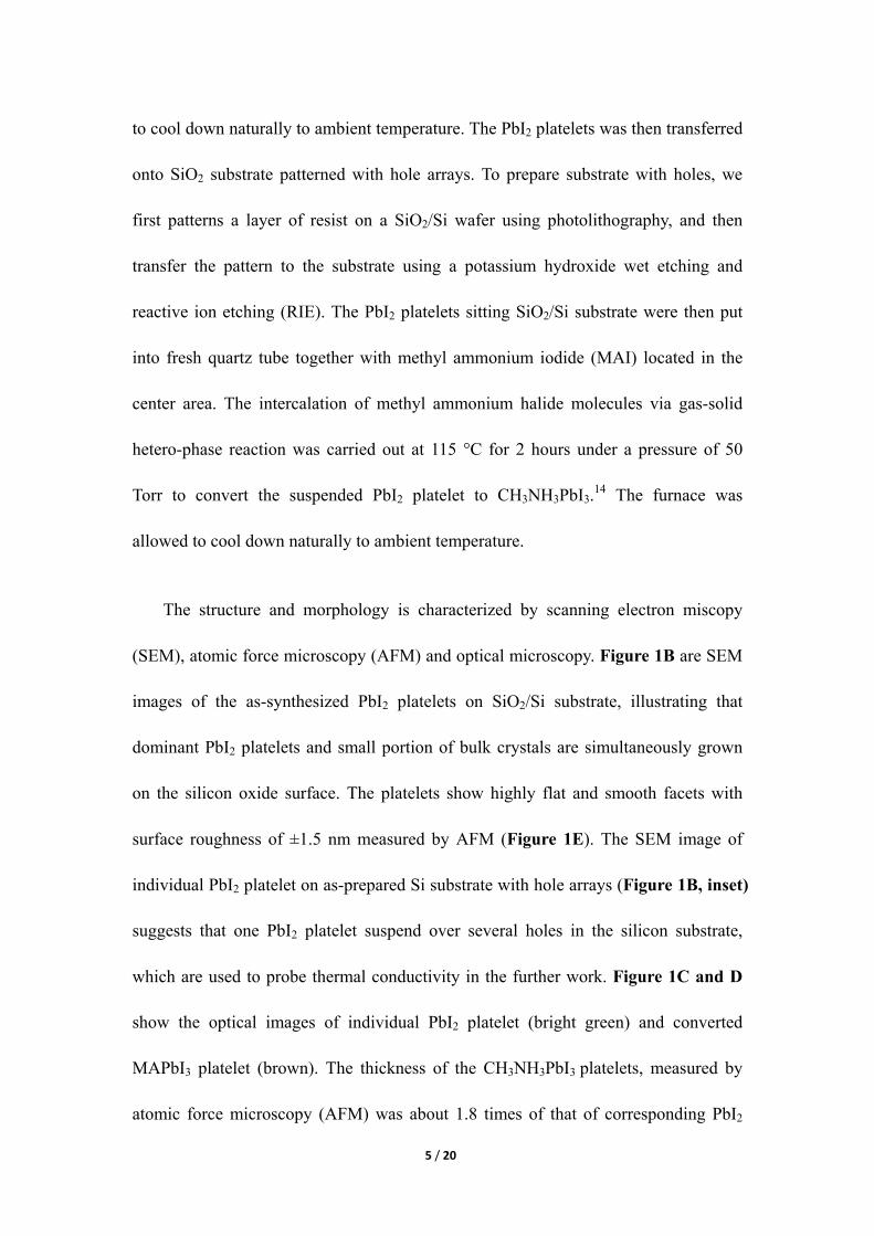
The structure and morphology is characterized by scanning electron miscopy
(SEM), atomic force microscopy (AFM) and optical microscopy. Figure 1B are SEM
images of the as-synthesized PbI2 platelets on SiO2/Si substrate, illustrating that
dominant PbI2 platelets and small portion of bulk crystals are simultaneously grown
on the silicon oxide surface. The platelets show highly flat and smooth facets with
surface roughness of ±1.5 nm measured by AFM (Figure 1E). The SEM image of
individual PbI2 platelet on as-prepared Si substrate with hole arrays (Figure 1B, inset)
suggests that one PbI2 platelet suspend over several holes in the silicon substrate,
which are used to probe thermal conductivity in the further work. Figure 1C and D
show the optical images of individual PbI2 platelet (bright green) and converted
MAPbI3 platelet (brown). The thickness of the CH3NH3PbI3 platelets, measured by
atomic force microscopy (AFM) was about 1.8 times of that of corresponding PbI2

6 / 20
platelets. It agrees well with the ratio of the c lattice constant between the two
compounds reported in previous studies, suggesting the successful conversion of PbI2
to MAPbI3.
To confirm the fully conversion of PbI2 to perovskite, Raman spectra of these
samples before and after conversion were conducted. In the measured range of 10 to
160 cm −1, the Raman spectra reveal four distinct bands at ~14, 70, 94, and 110 cm −1
as shown in Figure S3, which indicate that the CH3NH3PbI3 platelets maintain the 4H
polytype of PbI2. The phonon vibration located at ~14 cm−1 was assigned to , the
shear-motion rigid-layer mode of PbI2 with 4H polytype, while the Raman peaks at
~70, 94, and 110 cm−1 were assigned to , and , respectively. Figure 2A
shows x-ray diffraction pattern and optical microscopy images (inset) of
as-synthesized PbI2 platelet (upper panel) and MAPbI3 platelets after MAI
intercalation (bottom panel). Before conversion, due to the hexagonal structure of
PbI2, the XRD patterns exhibit four strong peaks at ~12.6°, 25.4°, 38.6° and 52.2°,
which are corresponding to crystal direction 001, 002, 003 and 004, which is in good
agreement with previous studies. After conversion, the identical peaks disappeared,
and several other peaks from tetragonal CH3NH3PbI3 were detected as shown in the
below part of Figure 2.15 The XRD pattern suggests a crystalline structure of the
as-grown perovskite. Peaks from PbI2 disappear suggesting the fully conversion from
PbI2 to CH3NH3PbI3. Fringe spacing (0.31 nm, see inset of Figure 2C) matches well
with the inter-planar spacing of the (220) plane from the tetragonal CH3NH3PbI3
crystal, while the fringe spacing of 0.70 nm in inset of Figure 2B matches well to the

7 / 20
inter-planar spacing of the (001) plane of the tetragonal PbI2. Moreover, the
absorption (blue dots) and PL (orange squares) spectroscopy of PbI2 and CH3NH3PbI3
platelets at room temperature also indicates successful conversion of PbI2 to
CH3NH3PbI3 (see Figure 2B and C). The absorption and PL spectroscopy of PbI2
platelets suggests absorption edge around 500 nm and single PL peak with Gaussian
profile centered at ~500 nm (Figure 2B). In MAPbI3 (Figure 2C), the absorption
edge and PL emission moves located at ~770 nm, which is consistent with band edge
emission of CH3NH3PbI3.14 The conversion time from PbI2 to CH3NH3PbI3 was
optimized to be 2 hours with the help of X-ray diffraction (XRD) study (Figure S2).
When the conversion time was too short (~ 1h),the PbI2 and CH3NH3PbI3 coexisted
from the XRD pattern. With the advance of time, the PbI2 peaks totally disappear at
the conversion complete stage.
In semiconductors, electronic and phonon structure including band gap and
phonon energy is highly dependent on temperature. For example, with the increasing
of temperature, semiconductor band gap become narrower because of the lattice
expansion. Therefore, band edge PL and Raman modes can be used as the temperature
indicator.16, 17 Both of PL and Raman spectroscopy are considered as reliable,
non-contact methods to probe local temperature of semiconductors. However,
CH3NH3PbI3 has low Raman scattering cross section. To do efficient temperature
measurement via Raman spectroscopy, excitation laser energy may be too high to
destroy sample. Considering outstanding emission properties of CH3NH3PbI3,
confocal PL microscopy is adopted to measure local temperature.

8 / 20
Figure 3A shows temperature dependent PL spectroscopy of individual MAPbI3
platelet. The power of pump laser (λ=532 nm) was kept as low as 5 μW to minimize
the laser heating effect. As temperature increases from 280 to 330 K, the MAPbI3
platelet on SiO2 substrate exhibits single emission peak due to band-edge emission,
which shifts monotonically from 771 nm (1.608 eV) to 767 nm (1.617 eV) (Figure
3A). The PL peak position shows blue shift with the increasing of temperature. The
widely-observed temperature dependent behavior in perovksite is different from that
in transitional technological-important semiconductors such as Si and GaAs 18,19. The
possible reason is the electron-phonon coupling and will be discussed in future. The
PL peak center energy E of CH3NH3PbI3 is extracted out and plotted versus
temperature T (Figure 3B), which could be well fitted as a linear function of
E=E0+α·T. The coefficient α is 0.16±0.02 meV/K within the temperature range from
280 K to 330 K. The linear PL emission energy as a function with temperature allows
us to easily monitor local temperature fluctuation by PL spectroscopy.
In order to measure the thermal conductivity properties, the MAPbI3 platelet was
then suspended to build an isolated thermal system to eliminate influence of
environment thermal conduction (Figure 3C). First of all, we conducted a detailed
analysis on the thermal dynamics for the isolated MAPbI3 system. In absorption and
emission process, the absorbed photons stimulate hot carriers with non-zero kinetic
energy, which then decay quickly to band edge and transfer their kinetic energy to the
lattice through scattering before recombination. Thermal equilibrium process of
photon generated hot carriers results in heating of samples. The heat can be

9 / 20
transported by three pathways: material conduction, gas convection and radiation. In
our case, the samples locate in vacuum and have small temperature differences with
environment, thus the gas convection and radiation can be negligible. Therefore, the
laser generated heat in the suspended area can only dissipate by conducting to
surrounding area along the platelet itself. According to Fourier's law, the thermal
conduction through cross-section of suspended sample is Q T dSκ= − ∇ ⋅ , where Q
is heating power per unit time, κ is thermal conductivity, ∇T is temperature gradient
of the cross sectional area element dS. As shown in Figure 3D, since SiO2/Si substrate
can be taken as a thermal reservoir, the temperature increase of non-suspended area is
small and undetectable. As a result, the temperature rise is strictly confined in
suspended area. After integrating differential form of Fourier's law from excitation
spot to the edge of suspended area in a two-dimensional circular geometry, the
thermal conductivity can be written as, ( / )Q Tκ γ= ⋅ Δ , where 2 1ln( / ) / 2R R hγ π= is
structure factor, ΔT is the energy difference between excitation laser spot position and
laser heated area and thermal reservoir. R1, R2, h is excitation laser spot diameter, hole
diameter and sample thickness, respectively. For a typical sample and thermal system,
the structure factor is a constant. The temperature difference between excitation spot
and thermal reservoir ∆T is linear to excitation laser power. Therefore, thermal
conductivity can be expressed as following equation:1 21 2( ) / ( )i iQ Q T Tκ γ= ⋅ − − , where
Ti1 and Ti2 are the laser excited area temperatures under heating powers Q1 and Q2,
respectively. According to above equation, the thermal conductivity can be extracted
out directly from power dependent photoluminescence spectroscopy.

10 / 20
Next, power dependence of PL spectroscopy of suspended MAPbI3 platelets is
conducted. A 532 nm solid state laser is adopted to obtain strong emission and ensure
high heat effect according to MAPbI3 absorption spectroscopy. For ultraviolet lasers,
the heat is too strong to damage the sample even under low power; for longer
wavelength lasers, the heating effect is too small to be detected. The laser power
was kept below 35 μW in our experiments to exclude band filling effect induced peak
shift.20 The laser spot radius is ~0.5 μm. As shown in Figure 4A-B, when excitation
laser power P increases from 10 μW to 35 μW, the PL peak shifts from 764.24 nm
(c.a. EPL =1.622 eV) to766.48 (c.a. EPL =1.617 eV). According to temperature
dependent PL spectroscopy (Fig. 3B), the peak shifts suggests temperature increase of
29.6 K. The PL emission energy is extracted out, which can be well fitted by a linear
function of laser power P (Figure 4C). The slope is δEPL/δP=0.26±0.01 meV/μW.
The effective power of laser excitation Q that contributes to thermal energy or
temperature increase of MAPbI3 is then evaluated. Firstly, the Equilibrium carriers
near to band carriers loss their energy through three recombination processes:
non-radiative, radiative, and Auger. For non-radiative and Auger processes, carriers
energy will converted to lattice vibration; while for radiative process, the carrier
energy will escape as photons. The laser excitation induced heating power Q can be
written as Q =P·β, where P is laser power, β is the heating factor. The heating factor β
can be written as ( ( ) / (1 ))laser PL PLp E E Eβ η η= ⋅ ⋅ + −− ; where Elaser = 2.33 eV and EPL
= 1.61 eV are respectively the laser photon energy and the averaged PL photon energy;
p is absorption rate, η is quantum yield. The PL quantum efficiency of CH3NH3PbI3 is

11 / 20
~90 ±5 % in our measurement because of the relatively small non-radiative and
Auger rate.21 The room temperature absorption coefficient of CH3NH3PbI3 at 532 nm
is about 5.5×104 cm-1, and the calculated absorption p is about 82% for 300 nm
platelets, which is in agreement with our absorption measurement using
micro-spectrometer.9 Thus, a heating factor of β = 0.31±0.1 is deduced which can be
used to calculate heating power. Combining the temperature coefficient of emission
peaks shift α =δE/δT=0.16±0.01 meV/K, heating factor β = 0.31±0.01 and the
structure factor γ = (7±1)×105 m-1, we obtained averaged thermal conductivity value
to be κ = 0.14±0.02 W/m·K.
To have a further understanding, we have measured the thermal conductivity of
CH3NH3PbI3 platelets with different thickness from ~80 to 400 nm, as shown in
Figure 5. The value of thermal conductivity keeps almost constant (~0.14 W/m·K) in
the range of 80-400 nm. Two obvious features can be concluded from the thickness
dependent measurement of thermal conductivity. Firstly, the measured values of ~0.14
W/m·K were at the same magnitude of single crystals of perovskite (0.5 W/m·K by
Pisoni et al.;12 0.3 W/m·K by Guo et al.;22 0.59 W/m·K by Qian et al.23) as reported in
previous literature; however, slightly smaller than these reported values. The interface
effect should play an important role in the thermal transport behavior due to the
suspended platelet configuration without any substrates in our experiments. For the
same reason, Guo et al. observed the reduction of thermal conductivity on Al2O3
substrate compared with that on Si substrate.22 Secondly, the thermal conductivity
shows no dependence on the layer thickness. This independence behavior

12 / 20
demonstrates the phonon surface scattering take almost no effects in this thickness
range (80-400 nm). Furthermore, the grain boundary scattering induced by the
morphological disorder can also be excluded because of the single crystal structure of
our samples. Therefore, the thickness independence of thermal conductivity indicates
that the uniformity of the as-grown perovskite single crystal platelet.
Conclusion
In summary, we reported a non-contact optical method to measure thermal
conductivity of single crystal MAPbI3 platelets. A measurement methodology and
derive expressions suitable for thermal conductivity evaluation for micro-sized
perovskite are explored. The substrate effect is minimized due to the advantage of
suspended configuration. Using this expression, thermal conductivity at room
temperature of κ=0.14±0.02 W/m·K is obtained for two-step CVD grown MAPbI3.
The thermal conductivity does not change with nanoplatelets thickness, suggesting
that the uniformity of as-prepared perovskite platelets. The ultra-low thermal
conductivity indicates that the MAPbI3 platelets can be a promising candidate,
especially very thin films, for thermal insulation and thermal electrics related usage.
Experimental methods
The crystalline structure and morphology are characterized by Atomic Force
Microscope (Veeco Dimension V), scanning electron microscopy (SEM, JEOL
7001F), X-ray diffraction (XRD; Bruker D8-Advance) and TEM (FEI Tecnai F20). A
WITec alpha300 RAS Raman system with a piezo crystal controlled scanning stage,
an objective lens of 100× magnification (numerical aperture, NA =0.95), and an

13 / 20
Electron Multiplying CCD was used for recording Raman spectra. All the Raman
spectra were recorded under an excitation laser of 532 nm (E laser = 2.33 eV).
Micro-PL spectroscopy of individual platelets is conducted by confocal triple-grating
spectrometer (Horiba-JY T6400) in a backscattering configuration. Micro-absorption
spectra from single perovskite platelet are measured on a home-made micro-based
measurement system. A 532 nm solid state laser is focused by an objective (Nikon,
50×, NA=0.45) and excites on platelets with beam diameter of ~1μm. The PL
emission signal is collected by the same objective and dispersed by monochromator
with 600 g/cm grating and then analyzed by liquid helium cooled charge-coupled
device (CCD, Princeton Instruments). A 532 nm long-pass filter is used to block
excitation laser line. Continuous-flow microscopy cryostat is used for
low-temperature PL spectra measurement. The SiO2/Si substrate with platelets was
pasted onto sample stage using GE vanish (Oxford Bearings Limited Company).
Acknowledgements
Q.Z acknowledges the support of start-up funding from Peking University,
one-thousand talent programs from Chinese government, open research fund program
of the state key laboratory of low-dimensional quantum physics. X.F.L thanks the
support from the Ministry of Science and Technology (No.2016YFA0200700),
National Natural Science Foundation of China (No.21673054), Key Research
Program of Frontier Science, CAS (No.QYZDB-SSW-SYS031) and Open Project of
Key Laboratory for UV-emitting Materials and Technology of Ministry of Education
(130028699). C.S thanks the support from NSFC Grant No. 11404324.
14 / 20
References
(1) Lee, M. M.; Teuscher, J.; Miyasaka, T.; Murakami, T. N.; Snaith, H. J. Efficient Hybrid Solar Cells Based on Meso-Superstructured Organometal Halide Perovskites. Science 2012, 338, 643-647.
(2) Burschka, J.; Pellet, N.; Moon, S. J.; Humphry-Baker, R.; Gao, P.; Nazeeruddin, M. K.; Gratzel, M. Sequential deposition as a route to high-performance perovskite-sensitized solar cells. Nature 2013, 499, 316-9.
(3) Liu, M. Z.; Johnston, M. B.; Snaith, H. J. Efficient planar heterojunction perovskite solar cells by vapour deposition. Nature 2013, 501, 395-8.
(4) Heo, J. H.; Im, S. H.; Noh, J. H.; Mandal, T. N.; Lim, C. S.; Chang, J. A.; Lee, Y. H.; Kim, H. J.; Sarkar, A.; Nazeeruddin, M. K.; Gratzel, M.; Seok, S. I. Efficient inorganic-organic hybrid heterojunction solar cells containing perovskite compound and polymeric hole conductors. Nat Photonics 2013, 7, 487-492.
(5) Park, N.-G.; Grätzel, M.; Miyasaka, T.; Zhu, K.; Emery, K. Towards stable and commercially available perovskite solar cells. Nature Energy 2016, 1, 16152.
(6) Bi, D.; Yi, C.; Luo, J.; Décoppet, J.-D.; Zhang, F.; Zakeeruddin, Shaik M.; Li, X.; Hagfeldt, A.; Grätzel, M. Polymer-templated nucleation and crystal growth of perovskite films for solar cells with efficiency greater than 21%. Nature Energy 2016, 1, 16142.
(7) Yuan, M.; Quan, L. N.; Comin, R.; Walters, G.; Sabatini, R.; Voznyy, O.; Hoogland, S.; Zhao, Y.; Beauregard, E. M.; Kanjanaboos, P.; Lu, Z.; Kim, D. H.; Sargent, E. H. Perovskite energy funnels for efficient light-emitting diodes. Nat Nano 2016, 11, 872-877.
(8) Yang, W. S.; Noh, J. H.; Jeon, N. J.; Kim, Y. C.; Ryu, S.; Seo, J.; Seok, S. I. High-performance photovoltaic perovskite layers fabricated through intramolecular exchange. Science 2015, 348, 1234-1237.
(9) Xing, G. C.; Mathews, N.; Lim, S. S.; Yantara, N.; Liu, X. F.; Sabba, D.; Gratzel, M.; Mhaisalkar, S.; Sum, T. C. Low-temperature solution-processed wavelength-tunable perovskites for lasing. Nat Mater 2014, 13, 476-480.
(10) Zhang, Q.; Ha, S. T.; Liu, X.; Sum, T. C.; Xiong, Q. Room-Temperature Near-Infrared High-Q Perovskite Whispering-Gallery Planar Nanolasers. Nano Letters 2014, 14, 5995-6001.
(11) Niu, L.; Zeng, Q.; Shi, J.; Cong, C.; Wu, C.; Liu, F.; Zhou, J.; Fu, W.; Fu, Q.; Jin, C.; Yu, T.; Liu, X.; Liu, Z. Controlled Growth and Reliable Thickness-Dependent Properties of Organic–Inorganic Perovskite Platelet Crystal. Advanced Functional Materials 2016, 26, 5263-5270.
(12) Pisoni, A.; Jaćimović, J.; Barišić, O. S.; Spina, M.; Gaál, R.; Forró, L.; Horváth, E. Ultra-Low Thermal Conductivity in Organic–Inorganic Hybrid Perovskite CH3NH3PbI3. The Journal of Physical Chemistry Letters 2014, 5, 2488-2492.
(13) Naikaew, A.; Prajongtat, P.; Lux-Steiner, M. C.; Arunchaiya, M.; Dittrich, T. Role of phase composition for electronic states in CH3NH3PbI3 prepared from CH3NH3I/PbCl2 solution. Applied Physics Letters 2015, 106.
(14) Ha, S. T.; Liu, X. F.; Zhang, Q.; Giovanni, D.; Sum, T. C.; Xiong, Q. H.

15 / 20
Synthesis of Organic-Inorganic Lead Halide Perovskite Nanoplatelets: Towards High-Performance Perovskite Solar Cells and Optoelectronic Devices. Adv Opt Mater 2014, 2, 838-844.
(15) Baikie, T.; Fang, Y.; Kadro, J. M.; Schreyer, M.; Wei, F.; Mhaisalkar, S. G.; Graetzel, M.; White, T. J. Synthesis and crystal chemistry of the hybrid perovskite (CH3NH3)PbI3 for solid-state sensitised solar cell applications. Journal of Materials Chemistry A 2013, 1, 5628-5641.
(16) Zhang, J.; Li, D. H.; Chen, R. J.; Xiong, Q. H. Laser cooling of a semiconductor by 40 kelvin. Nature 2013, 493, 504-508.
(17) Wehrenfennig, C.; Liu, M. Z.; Snaith, H. J.; Johnston, M. B.; Herz, L. M. Charge carrier recombination channels in the low-temperature phase of organic-inorganic lead halide perovskite thin films. Apl Mater 2014, 2.
(18) Odonnell, K. P.; Chen, X. Temperature-Dependence of Semiconductor Band-Gaps. Applied Physics Letters 1991, 58, 2924-2926.
(19) Yu, C. L.; Chen, Z.; Wang, J. J.; Pfenninger, W.; Vockic, N.; Kenney, J. T.; Shum, K. Temperature dependence of the band gap of perovskite semiconductor compound CsSnI3. J Appl Phys 2011, 110.
(20) Liu, X.; Zhang, Q.; Yip, J. N.; Xiong, Q.; Sum, T. C. Wavelength Tunable Single Nanowire Lasers Based on Surface Plasmon Polariton Enhanced Burstein–Moss Effect. Nano Letters 2013, 13, 5336-5343.
(21) Wehrenfennig, C.; Eperon, G. E.; Johnston, M. B.; Snaith, H. J.; Herz, L. M. High Charge Carrier Mobilities and Lifetimes in Organolead Trihalide Perovskites. Adv Mater 2014, 26, 1584-1589.
(22) Luo, Z. G. S. J. Y. J. S. M. P. V. K. a. T. Structural Phase- and Degradation-Dependent Thermal Conductivity of CH3NH3PbI3 Perovskite Thin Films. J. Phys. Chem. C 2016, 120, 8.
(23) Xin Qian, X. G., and Ronggui Yang. Lattice thermal conductivity of organic-inorganic hybrid perovskite CH3NH3PbI3. Applied Physics Letters 2016, 108.

Figu
Figuplatthe ConplatconvimaCH3
(C) platmeahighof th
ure and Ca
ure 1 (A) Stelets on hoPbI2 platele
nverting thetelets grownverted to C
ages of in
3NH3PbI3 pland (D) by
telets and Casured by Aher comparehe c lattice
aption
Schematic le arrays: Pets on SiO2 e suspendedn on SiO2/
CH3NH3PbI3
ndividual Platelet. (E)-y AFM charCH3NH3PbIAFM). The ed to the coconstant be
illustration PbI2 platelet
substrate ond PbI2 plat/Si substrate
3. The scalePbI2 platel-(F) ThicknracterizationI3 platelet cthickness o
orrespondinetween the tw
16 / 20
of the prepts being gronto the as-ptelet to CHe. The insee bar insideet and co
ness of PbI2
n. Note thacorrespondiof the CH3Nng PbI2 platewo compou
paration proown on SiO2
prepared Si H3NH3PbI3.et shows Se the imageorrespondin
2 platelet anat the differng to the d
NH3PbI3 plaelets, whichunds.
ocedures of
2/Si substratsubstrate w(B) SEM
EM image e is 5 μm. (g convertend CH3NH3
rence in coldifference iatelets was ah agrees we
f the perovsate; Transfer
with hole arrimage of
of after b(C)-(D) Oped product
3PbI3 platellor for the in thicknessabout 1.8 ti
ell with the r
skite rring ays; PbI2
being ptical t of et in PbI2
s (as imes ratio

Figuand peakCH3
as-gconvhighof 0PbI2
singFrinof th
ure 2 (A) Xafter conv
ks of PbI2 (
3NH3PbI3 wgrown PbI2 version. (Bh-resolution0.70 nm mat
2. The scalegle CH3NH3
nge spacinghe tetragona
XRD patterversion to C001, 002, 0were detect
platelet anB) The abson TEM (HRtches well te bar inside
3PbI3 platel of 0.31 nmal CH3NH3P
rn of the asCH3NH3PbI03, 004) disted. The upnd the loweorption and
RTEM) imagto the inter-e the imageets. Inset is
m matches wPbI3. The sc
17 / 20
s-grown CVI3 platelets sappeared, apper inset er inset is
d PL spectrge showing-planar space is 1 nm. (s a HRTEMwell to the icale bar insi
VD synthesi(below). A
and several shows the the photo
ra of singleg the lattice cing of the ((C) The abs
M image shonter-planar ide the imag
ized PbI2 pAfter conve
peaks belonmicroscopeof the sam
e PbI2 plateof crystal.
(001) plane sorption andowing the la
spacing of ge is 1 nm.
platelets (abersion, idenng to tetrage photo of
me platelet elets. Inset Fringe spa
of the hexad PL spectrattice of crythe (220) p
ove) ntical gonal
one after is a
acing agon ra of ystal. plane

Figutemrelacoefsetulasesubsconlase
ure 3 (A)mperature raation betweefficient was
up for the ner light focstrate. (D) ductivity ex
er. Red area
) Normalizange from 2en PL emiss obtained
non-contact used on a Zoom-in a
xtraction fois the suspe
zed PL spe280 to 330 sion peaks through thethermal coplatelet, w
area for der micro sizeended area.
18 / 20
ectra of sK, excitedand the tem
e linear fittonductivity which is sueducing the ed perovskiGray color
ingle CH3Nd by 532 nmmperature, ing slope. (measuremespended on
expressionite. Green sr area is the
NH3PbI3 pm laser at 5the peak sh(C) Schema
ent, it shownto holes an suitable fspot represeheat sink re
platelets in 5 μW. (B) hift temperaatic experim
ws the excitaarray on silfor the therents the focueservoir.
the The
ature ment ation licon rmal used

Figulaseoffsdiffeof bcollcon
ure 4 (A) Ner power; thset verticallferent laser pband edge lected fromfocal system
Normalizedhe laser wavly for claripowers to sPL peak en
m different sm. The mea
d PL spectrvelength is 5ty. (B) Zooshow the shnergy shift samples undsurement en
19 / 20
ra of one ty532 nm. Allomed PL d
hift clearly.with laser
der the lasenvironment
ypical suspl the spectradata of the (C) The expower diff
er excitationt was kept a
ended platea except the
suspendedperimental
fference. Thn of 532 nmt room temp
elet at diffee bottom oned platelet u
data and fithe spectra wm by usingperature.
erent e are
under tting were g the

FiguIn th
ure 5 Thickhe range of
kness depenf 80 to 400 n
ndent thermnm, the valu
20 / 20
mal conductiues of therm
ivity values mal conducti
for CH3NHivity keep a
H3PbI3 platealmost const
elets. tant.