thermal impact of thermal interface materials and …
TRANSCRIPT

THERMAL IMPACT OF THERMAL INTERFACE
MATERIALS AND HEAT SPREADER CO-
PLANARITY OF THE ELECTRONIC
PACKAGING
PANG SHI SHIANG
UNIVERSITI SAINS MALAYSIA
2020

THERMAL IMPACT OF THERMAL INTERFACE MATERIALS AND HEAT
SPREADER CO-PLANARITY OF THE ELECTRONIC PACKAGING
by
PANG SHI SHIANG
Thesis submitted in fulfilment of the
requirements for the degree of
Master of Science
June 2020

ii
ACKNOWLEDGEMENT
This thesis is a synergistic effort of many minds. It gives me a great pleasure to
witness the completion of the thesis that I would like to share my gratitude to those who
had given me relentless inspiration, wisdom, assistance and support.
First and foremost, I would like to express my appreciation to my thesis
supervisor, Prof. Ir. Dr. Mohd Zulkifly Abdullah, who had provided guidance,
supervision and advice throughout the research work. His patience and sacrifices to meet
up especially during weekends was very much valued and his inputs were instrumental
to the completion of this thesis.
Secondly, I would like to express my sincere gratitude to my company,
Broadcom Ltd, especially to Mr. Sam Karikalan who is my manager for the financial
support and motivation in this thermal research. Besides that, I am also thankful to my
technical lead, Dr. Zeki Celik for sharing his knowledge and guidance and nevertheless,
I am also grateful to my peer, Mr. Svensson Chai for sharing his knowledge and
participation in brainstorming activities throughout the research. They never failed to
assist me despites their busy schedules that I am indebted to them.
Lastly, I would like to take this opportunity to express my deepest gratitude to
my family members; my mother, my wife and my mother-in-law for their patience,
understanding, motivation and support in helping to take care of my twin children while
I am tied up with the research.

iii
TABLE OF CONTENTS
ACKNOWLEDGEMENT ............................................................................................. ii
TABLE OF CONTENTS ............................................................................................. iii
LIST OF TABLES ........................................................................................................ vi
LIST OF FIGURES ..................................................................................................... vii
LIST OF ABBREVIATIONS .................................................................................... xiii
ABSTRAK …………………………………………………………………………...xiv
ABSTRACT …………………………………………………………………………..xv
CHAPTER 1 INTRODUCTION ...................................................................................1
1.1 Introduction ............................................................................................................1
1.2 Problem Statement .................................................................................................3
1.3 Research Objectives ...............................................................................................5
1.4 Scopes .....................................................................................................................6
1.5 Outline of Thesis ....................................................................................................7
CHAPTER 2 LITERATURE REVIEW .......................................................................9
2.1 Introduction ............................................................................................................9
2.2 Flip Chip Package ..................................................................................................9
2.2.1 Flip Chip Package Construction .................................................................9
2.2.2 Reviews on Heat Spreader .......................................................................12
2.2.3 Reviews on Thermal Interface Material ...................................................13
2.3 Thermal Management of Flip Chip Package ........................................................19
2.3.1 Thermal Resistance ..................................................................................19
2.3.2 Heat Transfer Mechanisms .......................................................................23
Page

iv
2.4 Summary of Overall Literature Review ...............................................................28
CHAPTER 3 NUMERICAL AND EXPERIMENTAL INVESTIGATIONS .........30
3.1 Introduction ..........................................................................................................30
3.2 Numerical Approach ............................................................................................30
3.2.1 Computational Fluid Dynamics ................................................................30
3.2.2 Modelling of Package and Board .............................................................33
3.2.3 Simulation for Junction-to-Ambient ........................................................37
3.2.4 Simulation for Junction-to-Board .............................................................40
3.2.5 Simulation for Junction-to-Case ...............................................................42
3.2.6 Meshing ....................................................................................................44
3.3 Experimental Investigations .................................................................................49
3.3.1 Junction-to-Ambient Measurement and Data Validation .........................49
3.3.2 Junction-to-Board Measurement and Data Validation .............................51
3.3.3 Junction-to-Case Measurement and Data Validation ...............................53
3.4 Discussion and Summary .....................................................................................55
CHAPTER 4 COMPUTATIONAL FLUID DYNAMICS THERMAL ANALYSIS
………….………………………………………………………………………………56
4.1 Introduction ..........................................................................................................56
4.2 TIM1 Material ......................................................................................................57
4.3 Heat Spreader Co-planarity ..................................................................................63
4.3.1 Concave Profile ........................................................................................64
4.3.2 Convex Profile (Paste Type TIM1 Material) ...........................................69
4.3.3 Convex Profile (Film Type TIM1 Material) ............................................74
4.4 Discussions and Recommendations .....................................................................79
4.4.1 TIM1 Material Selection & Implementation ............................................79
4.4.2 Heat Spreader Co-planarity Tolerances ...................................................80

v
CHAPTER 5 CONCLUSION AND FUTURE RECOMMENDATIONS ...............84
5.1 Overall Conclusions .............................................................................................84
5.2 Limitations of Research ........................................................................................85
5.3 Recommendations for Future Research ...............................................................86
REFERENCES ..............................................................................................................88
APPENDIX A: JEDEC Thermal Characterization Standard
APPENDIX B: Lumped Model Calculations
APPENDIX C: Simulations Data Validation and Correlation
APPENDIX D: Simulations Data
APPENDIX E: TIM1 Datasheet
LIST OF PUBLICATIONS

vi
LIST OF TABLES
Page
Table 2.1 Package Material Thermal Conductivity List (IDT Application Note, 2014) . 10
Table 2.2 Convection Heat Transfer Coefficient (Cengel, 2004) .................................... 26
Table 2.3 Surface Emissivity of Common Electronic Materials (Cengel, 2004) ............ 28
Table 3.1 Material Assignment of the Test Board ........................................................... 34
Table 3.2 Material Assignment of the Package ............................................................... 35
Table 3.3 θJA Simulation Setup Summary ....................................................................... 38
Table 3.4 θJB and θJc Simulation Setup Summary ............................................................ 42
Table 3.5 θJA Measurements and Simulations Data Comparison .................................... 50
Table 3.6 θJB Measurements and Simulations Data Comparison .................................... 52
Table 3.7 θJC Measurements and Simulations Data Comparison .................................... 54
Table 4.1 Thermal Conductivities of Lumped Models .................................................... 57
Table 4.2 Material Properties of TIM1 Material ............................................................. 58
Table 4.3 Heat Transfer in θJA ......................................................................................... 60
vii
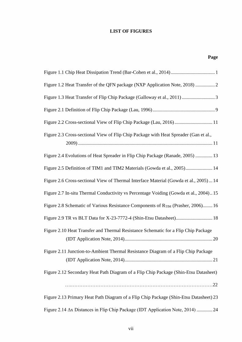
LIST OF FIGURES
Page
Figure 1.1 Chip Heat Dissipation Trend (Bar-Cohen et al., 2014) .................................... 1
Figure 1.2 Heat Transfer of the QFN package (NXP Application Note, 2018) ................ 2
Figure 1.3 Heat Transfer of Flip Chip Package (Galloway et al., 2011) ........................... 3
Figure 2.1 Definition of Flip Chip Package (Lau, 1996) ................................................... 9
Figure 2.2 Cross-sectional View of Flip Chip Package (Lau, 2016) ............................... 11
Figure 2.3 Cross-sectional View of Flip Chip Package with Heat Spreader (Gan et al.,
2009) .............................................................................................................. 11
Figure 2.4 Evolutions of Heat Spreader in Flip Chip Package (Ranade, 2005) .............. 13
Figure 2.5 Definition of TIM1 and TIM2 Materials (Gowda et al., 2005) ...................... 14
Figure 2.6 Cross-sectional View of Thermal Interface Material (Gowda et al., 2005) ... 14
Figure 2.7 In-situ Thermal Conductivity vs Percentage Voiding (Gowda et al., 2004) .. 15
Figure 2.8 Schematic of Various Resistance Components of RTIM (Prasher, 2006)........ 16
Figure 2.9 TR vs BLT Data for X-23-7772-4 (Shin-Etsu Datasheet).............................. 18
Figure 2.10 Heat Transfer and Thermal Resistance Schematic for a Flip Chip Package
(IDT Application Note, 2014) ........................................................................ 20
Figure 2.11 Junction-to-Ambient Thermal Resistance Diagram of a Flip Chip Package
(IDT Application Note, 2014) ........................................................................ 21
Figure 2.12 Secondary Heat Path Diagram of a Flip Chip Package (Shin-Etsu Datasheet)
….……………………………………………………………………………22
Figure 2.13 Primary Heat Path Diagram of a Flip Chip Package (Shin-Etsu Datasheet) 23
Figure 2.14 Δx Distances in Flip Chip Package (IDT Application Note, 2014) ............. 24

viii
Figure 3.1 Steps in CFD Simulations (Andersson et al., 2012) ....................................... 32
Figure 3.2 Package with JEDEC 2s2p Board Assembly ................................................. 33
Figure 3.3 Metal Layers of 2s2p Test Board ................................................................... 34
Figure 3.4 Modelling of a 40mm x 40mm Flip Chip Package ........................................ 36
Figure 3.5 Cross-sectional View of Flip Chip Package Modelling ................................. 36
Figure 3.6 Metal Layers of Substrate ............................................................................... 36
Figure 3.7 Isometric View of Junction-to-Ambient Modelling ....................................... 37
Figure 3.8 Temperature Distribution of θJA Simulation................................................... 39
Figure 3.9 Airflow Path of θJA Simulation....................................................................... 39
Figure 3.10 Airflow Pattern of θJA Simulation ................................................................ 40
Figure 3.11 Isometric View of Junction-to-Board Modelling ......................................... 41
Figure 3.12 Cross-sectional View of Junction-to-Board Modelling ................................ 41
Figure 3.13 Temperature Distribution of θJB Simulation ................................................. 42
Figure 3.14 Isometric View of Junction-to-Case Modelling ........................................... 43
Figure 3.15 Cross-sectional View of Junction-to-Case Modelling .................................. 44
Figure 3.16 Temperature Distribution of θJC Simulation ................................................. 44
Figure 3.17 Meshing Preview .......................................................................................... 46
Figure 3.18 Grid Dependency Study with Different Mesh Sizes .................................... 46
Figure 3.19 Mesh Quality (Face Alignment) ................................................................... 47
Figure 3.20 Mesh Quality (Volume) ................................................................................ 48
Figure 3.21 Mesh Quality (Skewness) ............................................................................. 48
Figure 3.22 θJA Measurement Setup ................................................................................ 50
Figure 3.23 θJB Measurement Setup ................................................................................ 52

ix
Figure 3.24 θJC Measurement Setup ................................................................................ 54
Figure 4.1 Simulation Data: θJA vs BLT for Various TIM1 Materials ............................ 59
Figure 4.2 Temperature Distribution of θJA Simulation (TIM1 material = X23-7772-4;
BLT = 0.12 mm) ............................................................................................ 60
Figure 4.3 Simulation Data: θJB vs BLT for Various TIM1 Materials ............................ 60
Figure 4.4 Temperature Distribution of θJB Simulation (TIM1 material = X23-7772-4;
BLT = 0.12 mm) ............................................................................................ 61
Figure 4.5 Simulation Data: θJC vs BLT for Various TIM1 Materials ............................ 61
Figure 4.6 Temperature Distribution of θJC Simulation (TIM1 material = X23-7772-4;
BLT = 0.12 mm) ............................................................................................ 62
Figure 4.7 Heat Spreader with Concave Profile Deflection ............................................ 64
Figure 4.8 Temperature Distribution of θJA Simulation (Concave Profile with 0.12 mm
Deflection) ..................................................................................................... 65
Figure 4.9 Simulation Data: θJA vs Deflection (Concave Profile) ................................... 66
Figure 4.10 Temperature Distribution of θJB Simulation (Concave Profile with 0.12 mm
Deflection) ..................................................................................................... 67
Figure 4.11 Simulation Data: θJB vs Deflection (Concave Profile) ................................. 67
Figure 4.12 Temperature Distribution of θJC Simulation (Concave Profile with 0.12 mm
Deflection) ..................................................................................................... 68
Figure 4.13 Simulation Data: θJC vs Deflection (Concave Profile) ................................. 68
Figure 4.14 Heat Spreader with Convex Profile (Paste Type TIM1 Material) ................ 69
Figure 4.15 Temperature Distribution of θJA Simulation (Convex Profile with Paste Type
TIM1 Material and 0.12 mm Deflection) ...................................................... 70
Figure 4.16 Simulation Data: θJA vs Deflection (Convex Profile with Paste Type TIM1
Material) ......................................................................................................... 71
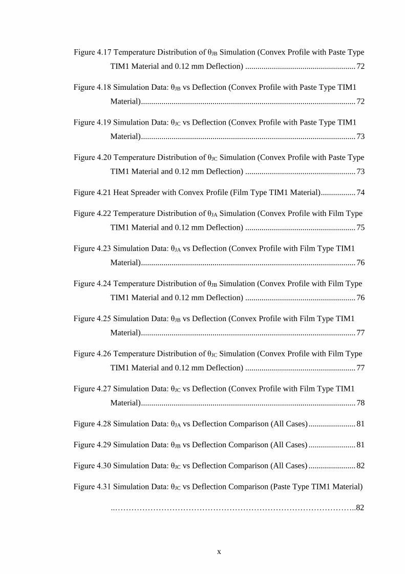
x
Figure 4.17 Temperature Distribution of θJB Simulation (Convex Profile with Paste Type
TIM1 Material and 0.12 mm Deflection) ...................................................... 72
Figure 4.18 Simulation Data: θJB vs Deflection (Convex Profile with Paste Type TIM1
Material) ......................................................................................................... 72
Figure 4.19 Simulation Data: θJC vs Deflection (Convex Profile with Paste Type TIM1
Material) ......................................................................................................... 73
Figure 4.20 Temperature Distribution of θJC Simulation (Convex Profile with Paste Type
TIM1 Material and 0.12 mm Deflection) ...................................................... 73
Figure 4.21 Heat Spreader with Convex Profile (Film Type TIM1 Material) ................. 74
Figure 4.22 Temperature Distribution of θJA Simulation (Convex Profile with Film Type
TIM1 Material and 0.12 mm Deflection) ...................................................... 75
Figure 4.23 Simulation Data: θJA vs Deflection (Convex Profile with Film Type TIM1
Material) ......................................................................................................... 76
Figure 4.24 Temperature Distribution of θJB Simulation (Convex Profile with Film Type
TIM1 Material and 0.12 mm Deflection) ...................................................... 76
Figure 4.25 Simulation Data: θJB vs Deflection (Convex Profile with Film Type TIM1
Material) ......................................................................................................... 77
Figure 4.26 Temperature Distribution of θJC Simulation (Convex Profile with Film Type
TIM1 Material and 0.12 mm Deflection) ...................................................... 77
Figure 4.27 Simulation Data: θJC vs Deflection (Convex Profile with Film Type TIM1
Material) ......................................................................................................... 78
Figure 4.28 Simulation Data: θJA vs Deflection Comparison (All Cases) ....................... 81
Figure 4.29 Simulation Data: θJB vs Deflection Comparison (All Cases) ....................... 81
Figure 4.30 Simulation Data: θJC vs Deflection Comparison (All Cases) ....................... 82
Figure 4.31 Simulation Data: θJC vs Deflection Comparison (Paste Type TIM1 Material)
..……………………………………………………………………………..82

xi
LIST OF SYMBOLS
Anominal Nominal area of heat transfer m2
Areal Real area of heat transfer m2
h Convection heat transfer coefficient W/m2. ⁰C
j∗ Radiant emittance of a black body W/m2
k Thermal conductivity of material W/m.K
P Applied pressure Pa
PH Heat dissipation of the device W
Qcond Heat flow by conduction W
Qconv Heat flow by convection W
Qrad Heat flow by radiation W
RBoard Thermal resistance of printed circuit board ⁰C/W
RBump Thermal resistance of solder bump ⁰C/W
RC Area-normalized thermal contact resistance K.m2/W
RDie Thermal resistance of die ⁰C/W
RDie/TIM Contact resistance of die to TIM ⁰C/W
RSub Thermal resistance of substrate ⁰C/W
RSB Thermal resistance of solder ball ⁰C/W
RTIM/HS Contact resistance of TIM to heat spreader ⁰C/W
RTIM Area-normalized thermal resistance K.m2/W
TA Ambient temperature ⁰C
TB Board temperature ⁰C
TC Case temperature ⁰C
TJ Junction temperature of the device ⁰C
ΔT
Δx
Temperature gradient in x direction K/m

xii
σ Constant of proportionality W/m2K4
σC Surface roughness of two contact surface m
ε Emissivity
ƟBA Thermal resistance board-to-ambient ⁰C/W
ƟCA Thermal resistance case-to-ambient ⁰C/W
ƟJA Thermal resistance junction-to-ambient ⁰C/W
ƟJB Thermal resistance junction-to-board ⁰C/W
ƟJC Thermal resistance junction-to-case ⁰C/W

xiii
LIST OF ABBREVIATIONS
BGA Ball Grid Array
BLT Bond Line Thickness
CFD Computational Fluid Dynamics
CTE Coefficient of Thermal Expansion
JEDEC Joint Electron Device Engineering Council
PCB Printed Circuit Board
POD Package Outline Drawing
QFN Quad Flat No-leads
TIM Thermal Interface Material
TIM1 Thermal Interface Material 1
TIM2 Thermal Interface Material 2

xiv
IMPAK TERMA BAGI BAHAN ANTARA MUKA TERMA DAN PENYEBAR
HABA BAGI PAKEJ ELEKTRONIK
ABSTRAK
Tesis ini membentangkan impak terma yang disebabkan oleh sifat-sifat bahan
antara muka terma dan kerataan penyebar haba ke atas pakej elektronik flip chip yang
diintegrasikan bersama penyebar haba. Bahan antara muka terma mempengaruh
kecekapan pemindahan haba dari silikon ke bungkusan pakej elektronik flip chip.
Kerataan penyebar haba mengubah prestasi terma dalam pakej elektronik flip chip
secara kerata, terutamanya rintangan pemindahan terma dari silikon ke bungkusan pakej
elektronik. Kajian berangka menggunakan ANSYS Icepak telah dijalankan untuk
menyiasat kesan terma yang disebabkan oleh sifat-sifat bahan antara muka terma dan
kemerosotan terma yang disebabkan oleh penyebar haba yang mempunyai pesongan
cekung atau cembung sebanyak 0.12 mm. Keputusan menunjukkan bahawa ketebalan
dan kekonduksian terma bahan antara muka terma mempengaruh prestasi pemindahan
haba dalam pakej elektronik flip chip. Keputusan juga menunjukkan bahawa pesongan
cekung menyebabkan penambahbaikan sebanyak 44 peratus sementara pesongan
cembung menyebabkan kemerosotan sebanyak 80 peratus ke atas rintangan terma dari
silikon ke bungkusan pakej elektronik flip chip. Hasil dari penyelidikan mencadangkan
panduan dan cadangan reka bentuk untuk pemilihan bersama pelaksanaan bahan antara
muka terma. Kekonduksian terma yang lebih tinggi dan bahan antara muka terma yang
lebih nipis harus dipilih untuk prestasi terma yang lebih baik untuk pakej elektronik flip
chip. Penemuan ini juga mengesyorkan toleransi kerataan kurang daripada 0.07 mm
untuk penyebar haba dalam pakej elektronik flip chip yang bersaiz 60 mm x 60 mm
dengan pelesapan haba sebanyak 150 W.

xv
THERMAL IMPACT OF THERMAL INTERFACE MATERIALS AND HEAT
SPREADER CO-PLANARITY OF THE ELECTRONIC PACKAGING
ABSTRACT
This thesis presents the thermal impact of thermal interface material 1 (TIM1)
and heat spreader co-planarity to the flip chip package with heat spreader. The TIM1
material influences the efficiency of heat transfer from silicon die to the heat spreader
while the co-planarity of heat spreader affects the thermal performance of the flip chip
package significantly, especially on the junction-to-case thermal resistance of the
package. Numerical studies using ANSYS Icepak were conducted to investigate the
thermal impact contributed by the TIM1 material properties and thermal degradation due
to heat spreader co-planarity in either concave or convex with deflections up to 0.12
mm. The result indicated that the bond line thickness (BLT) and the thermal
conductivity of the TIM1 material affected the thermal performance of the flip chip
package. The result also showed that with concave deflection improved up to 44 %
while convex deflection degraded up to 80 % of the junction-to-case thermal resistance
of the flip chip package. The outcome of the study is to propose design guidelines and
recommendations for TIM1 material selection and implementation. Higher thermal
conductivity and lower the BLT of TIM1 material shall be selected for better thermal
performance of the flip chip package. The findings also recommended the co-planarity
tolerance for the heat spreader shall not be greater than 0.07 mm for a 60 mm x 60 mm
flip chip package with a heat dissipation of 150 W.

1
CHAPTER 1
INTRODUCTION
1.1 Introduction
The heat dissipation of electronic packaging is a growing challenge over the
years due to demanding high performance and highly integrated functionalities of the
electronic packages ranging from the industry to consumer products. The chip heat
dissipation trend in the industries, such as the desktop, server and automotive
application are on rising trends in the past decade as presented by Bar-Cohen (2014).
The heat dissipation trend of the automotive application as illustrated in Figure 1.1
shows the heat dissipation is reaching 300 W with the heat flux around 240 W/cm2.
These electronic packages are processing big data at high speed, significantly produce
heat that needs to be dissipated into the environment. Therefore, thermal management
of electronic packages becomes very crucial to ensure the functionality, better
reliability and longer life span of the package.
Figure 1.1 Chip Heat Dissipation Trend (Bar-Cohen et al., 2014)

2
In most of the high heat dissipation electronic packaging, a heat spreader is
integrated to the electronic package to allow direct heat transfer from the silicon die in
either direction; through the bottom or the top of the packaging. Heat transfer through
the bottom occurs in downward direction to dissipate heat via the printed circuit board
such as Quad Flat No-leads (QFN) package. The heat transfer of the QFN package as
defined by NXP is shown in Figure 1.2. The QFN package usually has lower pin
counts and provides lesser electronic functionalities compared to Ball Grid Array
(BGA) packages. The downward direction will not be discussed in the research.
Figure 1.2 Heat Transfer of the QFN package (NXP Application Note, 2018)
On the other hand, the heat transfer through the top and dissipates heat in
upward direction through an external heat sink attached to the top of the packaging
such as the flip chip package with integrated heat spreader is studied and discussed. A
common example of the case study of the latter can be found is the microprocessor of
computer, which a highly thermal conductivity heat spreader that is made of copper,
placed at the top of the silicon die that helps to accelerate heat transfer from the silicon
die to an external heat sink. The heat will eventually dissipate into the environment by
a natural or forced air convection system. The heat transfer of the flip chip package

3
with heat spreader and an external heat sink as presented by Galloway et al. (2011) as
shown in Figure 1.3.
Figure 1.3 Heat Transfer of Flip Chip Package (Galloway et al., 2011)
The heat spreader is usually made by sheet metal forming and therefore,
inherits manufacturing tolerances such as the co-planarity and surface finishing
characteristics. When a heat spreader is required on a flip chip package, the thermal
interface material or known as the TIM1 material in the industry is introduced to fill
up the air gap between the silicon die and the heat spreader. The TIM1 material
functions to ensure effective heat transfer between the silicon die and the heat
spreader. Therefore, the TIM1 material and the co-planarity of heat spreader are the
key determination factors that vary the thermal resistance between junction and the
case of the package, which is known as junction-to-case thermal resistance, ƟJC. The
scope of this research is mainly to investigate the thermal impact of the TIM1 material
and the co-planarity of heat spreader to a flip chip electronic packaging using
computational fluid dynamics (CFD) simulation approach.
1.2 Problem Statement
Packaging thermal characterization data that comply with JEDEC standard is
pre-requisite for any new electronic package introduction into the market. These data
are made available to end users and could be found in all the package datasheets. The

4
characterization data include the junction-to-ambient thermal resistance or theta-JA
(ƟJA), the junction-to-board thermal resistance or theta-JB (ƟJB) and the junction-to-
case thermal resistance or theta-JC (ƟJC). ƟJA value is essential to the end user during
the heat sink selection in the system design as presented by Lee (1995) and to
determine whether a natural or forced air convection cooling design is needed. While
ƟJB and ƟJC are very crucial to the design engineer especially when the product
designer wants to predict the maximum junction temperature (TJUNCTION or TJ) of the
electronic package in the system using CFD simulation. Most of the CFD simulation
tools allow packaging modeling simplification by using two resistance model or also
known as 2R model without the need to build a detail packaging model in the
simulation as presented by Shidore et al. (2001) and (2007). The 2R model is defined
in JESD 15-3 (2008) and the 2R refers to the ƟJB and ƟJC values provided in the
package datasheet.
The thermal characterization data are generated from thermal simulation
analyses based on detailed packaging models which are modelled by the package
thermal engineer. Normally, thermal characterization analyses are carried out with the
assumptions that all parts in the packaging are at nominal and perfect conditions.
There is no co-planarity issue on all the parts and the TIM1 material fills up the air
gap between the silicon die and the heat spreader perfectly without any void.
However, in reality, the warpage can be easily found on the heat spreader and it
becomes even more severe when the package size is bigger with heat spreader of
larger surface area. The co-planarity of the heat spreader creates void in TIM1
material will eventually degrades the heat transfer from silicon die to the heat
spreader. As a result, the junction-to-case thermal resistance increases significantly.

5
Typically, for a flip chip package with a heat spreader, ƟJC in the range of 0.05
to 0.10 ⁰C/W as presented by Galloway et al. (2018). For a high power package, a
small variation of ƟJC value will cause a significant difference on TJ. For instance, a
package with a heat dissipation of 300 W undergo a variation of 0.05 ⁰C/W on ƟJC
will cause 15 ⁰C difference at the junction temperature. Therefore, the accuracy of ƟJC
value is very important in order to prevent overestimation or underestimation of the
maximum junction temperature of the package that will increase total product cost by
introducing unnecessary cooling system. A comprehensive investigation needs to be
carried out to further understand the relation and the impact of TIM1 material and co-
planarity of the heat spreader to a high power flip chip package.
1.3 Research Objectives
The objectives of this research are as the following:
a) To conduct steady state thermal simulation analysis to determine the
behavior of TIM1 material to the thermal performance of the flip chip
package.
b) To come out with simulation model that able to mimic the void created
by the heat spreader co-planarity and determine the impact to the
thermal performance of the flip chip package using CFD simulation
approach.
c) To come out with design recommendations and guidelines for future
package development based on the findings from simulation analysis.

6
1.4 Scopes
Thermal simulations that are carried out to investigate the thermal impact of
the TIM1 material and co-planarity of the heat spreader include the simulation to
characterize the junction-to-ambient thermal resistance, junction-to-board thermal
resistance and the junction-to-case thermal resistance of the package. The junction-to-
ambient thermal resistance simulations are in compliance with JEDEC, JESD51-2 and
JESD51-2A and run at natural convection environment until steady state are reached.
While the junction-to-board and junction-to-case thermal resistance simulations are
compliance with JEDEC, JESD51-8 and JESD51-14 (Draft) respectively. These
characterizations are simulated under pure conduction condition until steady state are
reached.
There are total of four different TIM1 materials with different thermal
conductivities and contact resistances are selected for the thermal performance
investigation. The thermal performance of TIM1 materials are compared at the severe
bond line thickness (BLT) of 0.08 mm, 0.12 mm and 0.16 mm with the assumptions
that the heat spreaders are perfectly flat without co-planarity issue.
Whereas, the heat spreader with concave and convex profiles with deflection
of 0.02 mm, 0.04 mm, 0.06 mm, 0.08 mm, 0.10 mm and 0.12 mm are investigated
under heat spreader co-planarity study. The TIM1 material is fixed to Shin-Etsu X23-
7772-4 with thermal conductivity, kTIM1 is 3.8 W/m.K and BLT is 0.12 mm in all the
heat spreader co-planarity investigations.

7
1.5 Outline of Thesis
There are a total of five chapters in this thesis. Chapter 1 discusses about the
current trend of the electronic packaging and provided some backgrounds on the
issues faced by electronic package engineer in the industry. Also stated are the
problem statement, objectives, scope of the research and the outline of this thesis.
Chapter 2 provides a comprehensive literature review to go through the
detailed construction and thermal management of a flip chip package. Several key
elements that influenced the thermal characteristic of the flip chip package are
addressed in this section.
Subsequently, Chapter 3 explains the simulation models used throughout the
research. The simulation modelling, meshing and boundary conditions are discussed
in detail. Last but not least, the evidence of correlation between simulation results and
the actual experimental measurement results are presented and subsequently these
simulation models with similar settings are used as the baselines for the future
simulations.
Chapter 4 presents the simulation results throughout this research. The
simulations are divided into two groups, the variation of TIM1 material and the co-
planarity of the heat spreader. The co-planarity of heat spreader includes the concave
deflection, convex deflection with paste type and film type TIM1 material
configurations. Discussion of the findings, design guidelines and recommendations
are presented at the end of the chapter.

8
The final chapter, Chapter 5 provides an overall conclusion from the
investigations, the limitations of the research and recommendations for the future
research.

9
CHAPTER 2
LITERATURE REVIEW
2.1 Introduction
This chapter presents the literature reviews based on JEDEC standards,
technical papers, patents, journals and final year projects from previous students. The
reviews of the flip chip package technology included the detailed constructions of the
flip chip package, the heat spreader technologies and the TIM1 materials in the flip
chip package. The thermal management of the flip chip package, mainly the thermal
resistances and heat transfer mechanism of a flip chip package are also being reviewed
in this chapter.
2.2 Flip Chip Package
2.2.1 Flip Chip Package Construction
Lau (1996) defined a flip chip as a chip that is attached to the pads of a
substrate or another chip with various interconnect materials and methods, as long as
the chip surface was facing the substrate as show in Figure 2.1.
Figure 2.1 Definition of Flip Chip Package (Lau, 1996)
10
Lau (1996) described that the chip or the silicon die is bumped before flipped
onto a substrate. The bumps are distributed across the entire chip and not only located
on the die edge and therefore intellectual property (IP) blocks could be placed all over
the surface of the die. This allows designer to place more IP blocks per die, which
reduces the chip size and optimise signal integrity. The substrate provides connectivity
from silicon die to the external print circuit board via bumps and solders balls. It also
absorbs heat from silicon die via bumps and dissipates heat to the print circuit board
via solder balls. The underfill material is used to fill the air gap between the bumps,
silicon die and the substrate, providing better adhesion of the silicon die to the
substrate. At the same time, underfill also helps in heat transfer between silicon die
and the substrate as the underfill thermal conductivity is usually higher than air as
listed in Table 2.1. The cross-sectional view of the flip chip package is shown in
Figure 2.2.
Table 2.1 Package Material Thermal Conductivity List (IDT Application Note, 2014)

11
Figure 2.2 Cross-sectional View of Flip Chip Package (Lau, 2016)
For a high power flip chip package, a heat spreader is placed on top of the
silicon die to provide more superior heat transfer from silicon die to the external
environment. And the heat spreader is usually made of high thermal conductivity
material such as copper with k = 387.6 W/m.K. A thermal interface material (TIM)
would be used as the gap filler to fill up the air gap between silicon die and the heat
spreader and therefore provide more effective heat conduction between silicon die and
the heat spreader. The cross-sectional view of a flip chip package with integrated heat
spreader as presented by Gan et al. (2009) is shown in Figure 2.3.
Figure 2.3 Cross-sectional View of Flip Chip Package with Heat Spreader (Gan et al.,
2009)

12
2.2.2 Reviews on Heat Spreader
The evolution of flip chip package was described by Ranade (2005) in the
article ‘Packaging Technology Ready for Change’. The flip chip package has evolved
from the drivers such as performance, cost, I/O density and thermal impedance have
pushed the package designers to develop suitable solutions instead of ‘one size fits all’
solutions in the traditional flip chip package design. The thermal impedance and cost
that drove the subcomponent costs reduction on the flip chip package has pushed for
the evolution of heat spreader design in flip chips.
The outlines of the evolution of heat spreader design in flip chip packages are
shown in Figure 2.4. A single piece of stamped heat spreader that pushed the Ni-
plated stiffener and heat spreader combination to the end is driven by the process
simplification and cost. Future improvements include a strip format overmolded
substrates with drop-in heat spreaders or simple bare die with direct attachment of
heat sinks as presented by Ranade (2005).

13
Figure 2.4 Evolutions of Heat Spreader in Flip Chip Package (Ranade, 2005)
2.2.3 Reviews on Thermal Interface Material
Gowda et al. (2005) explained the thermal interface material between silicon
die and heat spreader is typically designated as TIM1 and the thermal interface
material between heat spreader and an external heat sink is designated as TIM2 as
shown in Figure 2.5. The thermal interface material solutions exist in several forms,
such as adhesive, greases, gels, phase change material and pads. Each of these TIM
solutions have certain advantages and disadvantages. Most of the thermal interface
materials consist of polymer matrix, such as an epoxy or silicone resin and thermally
conductive filler such as boron nitride, alumina, aluminium, zinc oxide and silver.

14
Figure 2.5 Definition of TIM1 and TIM2 Materials (Gowda et al., 2005)
Gowda et al. (2005) further described several performance metrics that were
used to describe the thermal performance of the thermal interface material namely, the
thermal conductivity, apparent or in-situ conductivity, thermal resistance and thermal
impedance. Thermal conductivity is the ability to conduct heat across the material.
Apparent or in-situ conductivity takes into account of the contact resistances between
thermal interface material and the interface components. In fact, the apparent or in-situ
conductivity more precisely represents the actual performance of the thermal interface
material. Thermal resistance and impedance represent the resistances of heat flow
across the interface material. Figure 2.6 illustrates the cross-sectional view of thermal
interface material.
Figure 2.6 Cross-sectional View of Thermal Interface Material (Gowda et al., 2005)

15
In another publication, Gowda et al. (2004) also reported the effect of void and
their characteristics to the thermal performance of the TIM material adhesive layers.
Voids were quantified and experimented to check for the in-situ thermal conductivity
for several TIM materials, as shown in Figure 2.7. The report showed that the
increasing of void sizes in the TIM materials decrease the in-situ thermal conductivity
of the TIM materials that applicable to both of the TIM1 and TIM2 materials.
However, the voids are investigated independently and the relation of void created due
the co-planarity of heat spreader is not addressed in the study.
Figure 2.7 In-situ Thermal Conductivity vs Percentage Voiding (Gowda et al., 2004)
Mahajan (2004) described after inserting a thermal interface material to solid
surfaces, the effective thermal resistance, RTIM, at the interface will have two
components. The bulk resistance, Rbulk, of the thermal interface material arising from
its finite thermal conductivity and the contact resistance, RC between the thermal
interface material and the adjoining solids, as shown in Figure 2.8. RTIM can be
calculated from Equation 1, this applicable to both of the TIM1 and TIM2 materials.

16
Figure 2.8 Schematic of Various Resistance Components of RTIM (Prasher, 2006)
(1)
Where RTIM = area-normalized thermal resistance of TIM (K.m2/W)
BLT = bond line thickness of TIM (m)
kTIM = thermal conductivity of TIM (W/m.K)
RC1 & RC2 = area-normalized thermal contact resistances (K.m2/W)
In order to optimise the heat transfer by conduction, RTIM should be
minimized. This could be accomplished by reducing the BLT, increase thermal
conductivity and reduce the contact resistances RC1 and RC2.
𝑹𝑻𝑰𝑴 = 𝑩𝑳𝑻
𝒌𝑻𝑰𝑴+ 𝑹𝑪𝟏 + 𝑹𝑪𝟐

17
Prasher et al. (2003) addressed the bond line thickness is a function of various
parameters such as the application pressure and the particle volume fraction. The bond
line thickness could be calculated from Equation 2. The higher the application
pressure onto the thermal interface material would reduce the bond line thickness and
thus reduce the thermal resistance of thermal interface material.
(2)
Where BLT = bond line thickness of TIM (m)
𝞽y = yield stress of TIM (MPa)
P = applied pressure (Pa)
Prasher et al. (2001) stated that the total of contact resistances of the thermal
interface material could be determined by Equation 3.
(3)
Where RC1+2 = total contact resistances (K.m2/W)
σ1 & σ2 = surface roughness of two contact surfaces (m)
kTIM = thermal conductivity of TIM (W/m.K)
Anominal = nominal area of heat transfer (m2)
Areal = real area of heat transfer (m2)
Areal is always smaller than the nominal contributed by the air trapped in the
wetting area. The contact resistance could be minimized by decreasing the surface
𝑩𝑳𝑻 = 𝟏. 𝟑𝟏 𝒙 𝟏𝟎−𝟒 (𝞽𝒚
𝑷)
𝟎.𝟏𝟔𝟔
𝑹𝑪𝟏+𝟐 = (𝝈𝟏+𝝈𝟐
𝟐𝒌𝑻𝑰𝑴) (
𝑨𝒏𝒐𝒎𝒊𝒏𝒂𝒍
𝑨𝒓𝒆𝒂𝒍)

18
roughness, increase the thermal conductivity of interface material and minimise the air
trapped in the interface area.
The thermal resistance versus bond line thickness chart (TR vs BLT) could be
found in the thermal interface material datasheet. For instance, the TR vs BLT chart
for X-23-7772-4 TIM1 material from Shin-Etsu is shown in Figure 2.9. The thermal
conductivity shown in the chart represents the apparent thermal conductivity which is
always lower than the bulk thermal conductivity, 3.8 W/m.K as given in the datasheet.
The thermal contact resistance given in the TR vs BLT graph could be referred to the
total contact resistance across the interface material which consisted of the contact
resistances on the top and the bottom of the interface material as shown in Figure 2.6
and Figure 2.8. This explains why the apparent or in situ thermal conductivity is
essential for package development during thermal interface material selection.
Figure 2.9 TR vs BLT Data for X-23-7772-4 (Shin-Etsu Datasheet)
19
2.3 Thermal Management of Flip Chip Package
2.3.1 Thermal Resistance
The application note of IDT (2014) explained that thermal resistance is the
measure of a material’s capability to resist the heat flow which could be in the form of
conduction, convection or radiation. Thermal resistance is commonly used to evaluate
and compare the thermal performance of the electronic package based on JEDEC
standard. The relationship between thermal resistance, heat flow and the temperature
differences is shown in Equation 4.
(4)
Where Ɵ = thermal resistance (⁰C/W)
ΔT = temperature differences across the material (⁰C)
P = heat flow or the power applied to the material (W)
IDT (2014) further described that junction-to-ambient thermal resistance (ƟJA)
measured the ability of a package to dissipate heat from the silicon die to the ambient
environment through convection and radiation. The junction-to-ambient thermal
resistance (ƟJA) under this condition could be determined from Equation 5 as defined
in JEDEC standard, JESD 51-2 and JESD 51-2A.
(5)
Where ƟJA = thermal resistance from junction-to-ambient (⁰C/W)
TJ = junction temperature of the device at steady state (⁰C)
Ɵ = 𝜟𝑻
𝑷
ƟJA
= 𝑻𝑱 −𝑻𝑨
𝑷𝑯
20
TA = ambient temperature at steady state (⁰C)
PH = heat dissipation of the device (W)
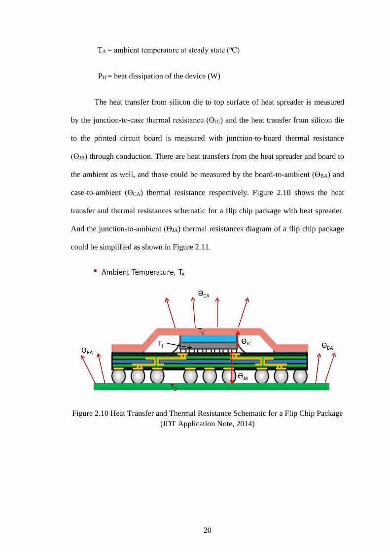
The heat transfer from silicon die to top surface of heat spreader is measured
by the junction-to-case thermal resistance (ƟJC) and the heat transfer from silicon die
to the printed circuit board is measured with junction-to-board thermal resistance
(ƟJB) through conduction. There are heat transfers from the heat spreader and board to
the ambient as well, and those could be measured by the board-to-ambient (ƟBA) and
case-to-ambient (ƟCA) thermal resistance respectively. Figure 2.10 shows the heat
transfer and thermal resistances schematic for a flip chip package with heat spreader.
And the junction-to-ambient (ƟJA) thermal resistances diagram of a flip chip package
could be simplified as shown in Figure 2.11.
Figure 2.10 Heat Transfer and Thermal Resistance Schematic for a Flip Chip Package
(IDT Application Note, 2014)

21
Figure 2.11 Junction-to-Ambient Thermal Resistance Diagram of a Flip Chip Package
(IDT Application Note, 2014)
Junction-to-board thermal resistance (ƟJB) is used to measure the conduction
of heat from silicon die to the print circuit board. The junction-to-board thermal
resistance (ƟJB) under this condition could be determined from Equation 6 according
to JEDEC standard, JESD 51-8.
(6)
Where ƟJB = thermal resistance from junction-to-board (⁰C/W)
TJ = junction temperature of the device at steady state (⁰C)
TB = board temperature at steady state (⁰C)
PH = heat dissipation of the device (W)
Heat conduction from the silicon die to the printed circuit board is shown in
Figure 2.12. Each of the silicon die, bumps, underfill, substrate, solderballs and board
ƟJB
= 𝑻𝑱 −𝑻𝑩
𝑷𝑯

22
has its own thermal resistance. The junction-to-board thermal resistance of the
package is the summation of all these thermal resistances and could be calculated
from Equation 7.
Figure 2.12 Secondary Heat Path Diagram of a Flip Chip Package (Shin-Etsu
Datasheet)
(7)
Junction-to-case thermal resistance (ƟJC) measured the ability of a package to
conduct heat from silicon die to case. The junction-to-case thermal resistance (ƟJC)
under this condition could be determined from Equation 8:
(8)
Where ƟJC = thermal resistance from junction-to-case (⁰C/W)
TJ = junction temperature of the device at steady state (⁰C)
TC = case temperature at steady state (⁰C)
PH = heat dissipation of the device (W)
Figure 2.13 shows the detailed heat path from the active side of die to the top
of lid, heat spreader. Each of the components such as silicon die, TIM1 material and
ƟJC
= 𝑻𝑱 −𝑻𝑪
𝑷𝑯
ƟJB
= RJB
= RDie
+ RBump
+ RSub
+ RSB
+ RBoard

23
heat spreader has its own thermal resistance. There are two contact resistances along
the heat path, one at the top and another at the bottom of the TIM1 material. The
existence of these two contact resistances are contributed by the bond line thickness
between TIM1 material with the silicon die and the heat spreader. The contact
resistance is contributed by the surface roughness of the parts itself. The summation of
these thermal resistances develops the junction-to-case thermal resistance of the
package and could be summarized and calculated from Equation 9.
Figure 2.13 Primary Heat Path Diagram of a Flip Chip Package (Shin-Etsu Datasheet)
(9)
2.3.2 Heat Transfer Mechanisms
According to heat transfer textbook by Cengel (2004), there are three modes of
heat transfer occurred in a system, for instance the heat dissipation from a
semiconductor packaging to the ambient. Heat can be transferred by conduction,
convection and radiation.
Conduction is the measured of heat transfer between two material that are in
direct contact. Fourier’s law of heat conduction states that the time rate of heat
transfer though a material is proportional to the negative of temperature gradient and
ƟJC
= RJC
= RDie
+ RDie/TIM
+ RTIM
+ RTIM/HS
+ RHS
24
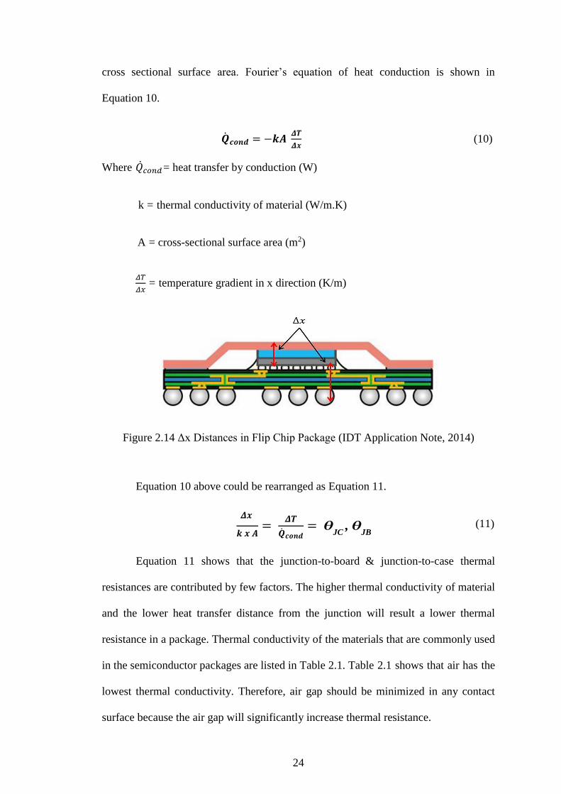
cross sectional surface area. Fourier’s equation of heat conduction is shown in
Equation 10.
��𝒄𝒐𝒏𝒅 = −𝒌𝑨 𝜟𝑻
𝜟𝒙 (10)
Where ��𝑐𝑜𝑛𝑑 = heat transfer by conduction (W)
k = thermal conductivity of material (W/m.K)
A = cross-sectional surface area (m2)
𝛥𝑇
𝛥𝑥 = temperature gradient in x direction (K/m)
Figure 2.14 Δx Distances in Flip Chip Package (IDT Application Note, 2014)
Equation 10 above could be rearranged as Equation 11.
(11)
Equation 11 shows that the junction-to-board & junction-to-case thermal
resistances are contributed by few factors. The higher thermal conductivity of material
and the lower heat transfer distance from the junction will result a lower thermal
resistance in a package. Thermal conductivity of the materials that are commonly used
in the semiconductor packages are listed in Table 2.1. Table 2.1 shows that air has the
lowest thermal conductivity. Therefore, air gap should be minimized in any contact
surface because the air gap will significantly increase thermal resistance.
𝜟𝒙
𝒌 𝒙 𝑨=
𝜟𝑻
��𝒄𝒐𝒏𝒅= Ɵ
JC , Ɵ
JB