thermoelectric cooler (tec) controller data sheet · pdf filethermoelectric cooler (tec)...
TRANSCRIPT

Thermoelectric Cooler (TEC) Controller Data Sheet ADN8831
Rev. A Information furnished by Analog Devices is believed to be accurate and reliable. However, no responsibility is assumed by Analog Devices for its use, nor for any infringements of patents or other rights of third parties that may result from its use. Specifications subject to change without notice. No license is granted by implication or otherwise under any patent or patent rights of Analog Devices. Trademarks and registered trademarks are the property of their respective owners.
One Technology Way, P.O. Box 9106, Norwood, MA 02062-9106, U.S.A. Tel: 781.329.4700 www.analog.com Fax: 781.461.3113 ©2005–2012 Analog Devices, Inc. All rights reserved.
FEATURES Two integrated zero drift, rail-to-rail, chop amplifiers TEC voltage and current operation monitoring Programmable TEC maximum voltage and current Programmable TEC current heating and cooling limits Configurable PWM switching frequency up to 1 MHz Power efficiency: > 90% Temperature lock indication Optional internal or external clock source Clock phase adjustment for multiple drop operation Supports negative temperature coefficient (NTC) thermistors
or positive temperature coefficient (PTC) resistance thermal detectors (RTDs)
5 V typical and optional 3 V supplies Standby and shutdown mode availability Adjustable soft start feature 5 mm × 5 mm 32-lead LFCSP
APPLICATIONS Thermoelectric cooler (TEC) temperature control DWDM optical transceiver modules Optical fiber amplifiers Optical networking systems Instruments requiring TEC temperature control
GENERAL DESCRIPTION The ADN8831 is a monolithic TEC controller. It has two inte-grated, zero drift, rail-to-rail comparators, and a PWM driver. A unique PWM driver works with an analog driver to control external selected MOSFETs in an H-bridge. By sensing the thermal detector feedback from the TEC, the ADN8831 can drive a TEC to settle the programmable temperature of a laser diode or a passive component attached to the TEC module.
The ADN8831 supports NTC thermistors or positive tempera-ture coefficient (PTC) RTDs. The target temperature is set as an analog voltage input either from a DAC or from an external resistor divider driven by a reference voltage source.
A proportional integral differential (PID) compensation network helps to quickly and accurately stabilize the ADN8831 thermal control loop. An adjustable PID compensation network example is described in the AN-695 Application Note, Using the ADN8831 TEC Controller Evaluation Board. A typical reference voltage of 2.5 V is available from the ADN8831 for thermistor temperature sensing or for TEC voltage/current measuring and limiting in both cooling and heating modes.
FUNCTIONAL BLOCK DIAGRAM
AMPLIFIERChop2
AMPLIFIERChop1
IN1P
IN1N
OUT1
IN2P
IN2N
OUT2
LIMITER/MONITOR
REF SOFT STARTSHUTDOWN OSCILLATOR
TMPGD VREF SS/SB PHASE FREQSYNCI/SD
LINEARMOSFETDRIVER
PWMMOSFETDRIVER
LFB
LPGATE
LNGATE
SFB
SPGATE
SNGATE
COMPSW
SW
COMPOSC
SYNCO
CONTROL
ILIMC ILIMH ITEC VLIM VTEC CS
0466
3-00
1
Figure 1.

ADN8831 Data Sheet
Rev. A | Page 2 of 20
TABLE OF CONTENTS Features .............................................................................................. 1 Applications ....................................................................................... 1 General Description ......................................................................... 1 Functional Block Diagram .............................................................. 1 Revision History ............................................................................... 2 Detailed Block Diagram .................................................................. 3 Specifications ..................................................................................... 4
Electrical Characteristics ............................................................. 4 Absolute Maximum Ratings ............................................................ 6
Thermal Characteristics .............................................................. 6 ESD Caution .................................................................................. 6
Pin Configuration and Function Descriptions ............................. 7 Typical Performance Characteristics ............................................. 9 Theory of Operation ...................................................................... 11
Oscillator Clock Frequency ....................................................... 12 Oscillator Clock Phase ............................................................... 12
Temperature Lock Indicator ..................................................... 13 Soft Start on Power-Up .............................................................. 13 Shutdown Mode ......................................................................... 13 Standby Mode ............................................................................. 13 TEC Voltage/Current Monitor ................................................. 13 Maximum TEC Voltage Limit .................................................. 13 Maximum TEC Current Limit ................................................. 14
Applications Information .............................................................. 15 Signal Flow .................................................................................. 15 Thermistor Setup ........................................................................ 15 Thermistor Amplifier (Chop1) ................................................ 15 PID Compensation Amplifier (Chop2) .................................. 16 MOSFET Driver Amplifier ....................................................... 17
Outline Dimensions ....................................................................... 18 Ordering Guide .......................................................................... 18
REVISION HISTORY 8/12—Rev. 0 to Rev. A
Changes to Features and General Description Sections .............. 1 Moved Figure 2 ................................................................................. 3 Changes to Figure 2 .......................................................................... 3 Changes to Table 1 ............................................................................ 4 Changes to Table 2 and Table 3 ....................................................... 6 Changes to Figure 3 and Table 4 ..................................................... 7 Changes to Theory of Operation Section and Figure 12 ........... 11 Changes to Figure 14 and Figure 15 ............................................. 11 Changes to Oscillator Clock Frequency Section and Oscillator Clock Phase Section ....................................................................... 12 Changes to Soft Start on Power-Up Section, Shutdown Mode Section, Standby Mode Section, and TEC Voltage/Current Monitor Section .............................................................................. 13 Changes to Figure 17 ...................................................................... 15 Changes to PID Compensation Amplifier (Chop2) Section .... 16 Changes to MOSFET Driver Amplifier Section and Figure 21 .. 17 Updated Outline Dimensions ....................................................... 18 Changes to Ordering Guide .......................................................... 18
9/05—Revision 0: Initial Version

Data Sheet ADN8831
Rev. A | Page 3 of 20
DETAILED BLOCK DIAGRAM
ADN8831
REFERENCE
VB
1.25V
80kΩ2kΩ
10kΩ
8
7
6
5
4
3
2
1ILIMC
IN1P
IN1N
OUT1
IN2P
IN2N
OUT2
32 31 30 29 28 27 26 25
24
22
21
18
17
1615141211109
TEMPERATUREGOOD
2.5V
20
19
COMPSW
SFB
PGND
SNGATE
DR
IVER
SW
SPGATE
PVDD
COMPOSCSOFT START
SB250mV
OSCILLATOR
SD
SDDETECT
13
ITEC
ILIMC
ILIMH100kΩ
100kΩ
20kΩ
20kΩ
LFB
LINEAR AMPLIFIER
LPGATELNGATELFB
VB
VC
23VB
gm3
gm2
gm1VC
20kΩ20kΩ
20kΩ
20kΩ
1.25V
1.25V
VB
Chop2
Chop1
VB= 2.5V, VDD > 4.0V= 1.5V, VDD < 4.0V
ILIMH VLIM VTEC ITEC CS
VOLTAGELIMIT
25kΩ
20kΩ 20kΩ
5kΩ
SFB LFB
1.25V1kΩ
25kΩ
VREF
0466
3-00
3
5kΩ
1kΩ
AVDD PHASE TMPGD AGND FREQ SYNCO SYNCI/SDSS/SB Figure 2. Detailed Block Diagram

ADN8831 Data Sheet
Rev. A | Page 4 of 20
SPECIFICATIONS ELECTRICAL CHARACTERISTICS VDD = 3.0 V to 5.0 V, TA = 25°C, unless otherwise noted. Table 1. Parameter1 Symbol Test Conditions/Comments Min Typ Max Unit PWM OUTPUT DRIVER
Output Transition Time tR, tF CL = 3300 pF 20 ns Nonoverlapping Clock Delay 40 80 ns Output Resistance RO (SNGATE, SPGATE) IL = 10 mA, VDD = 3.0 V 6 Ω Output Voltage Swing2 SFB VLIM = VREF 0 VDD V
LINEAR OUTPUT AMPLIFIER Output Resistance RO, LNGATE IOUT = 2 mA, VDD = 3.0 V 200 Ω RO, LPGATE IOUT = 2 mA, VDD = 3.0 V 100 Ω Output Voltage Swing2 LFB 0 VDD V
POWER SUPPLY Power Supply Voltage VDD 3.0 5.5 V Supply Current ISY PWM not switching 8 12 mA −40°C ≤ TA ≤ +85°C 15 mA Shutdown Current ISD SYNCI/SD = 0 V 8 µA
Soft Start Charging Current ISS VSS = 0 V 8 µA Undervoltage Lockout3 UVLO Low to high threshold 2.2 2.6 V Standby Current ISB SYNCI/SD = VDD, SS/SB = 0 V 2 mA
Standby Threshold VSB SYNCI/SD = VDD 150 200 mV
ERROR/COMPENSATION AMPLIFIERS Input Offset Voltage VOS1 VCM1 = 1.5 V, VIN1P − VIN1M 10 100 μV VOS2 VCM2 = 1.5 V, VIN2P − VIN2M 10 100 μV Input Voltage Range VCM1, VCM2 0 VDD V Common-Mode Rejection Ratio CMRR1, CMRR2 VCM1, VCM2 = 0.2 V to VDD − 0.2 V 120 dB Output Voltage High VOH1, VOH2 VDD − 0.03 V Output Voltage Low VOL1, VOL2 25 mV Power Supply Rejection Ratio PSRR1, PSRR2 3.0 V ≤ VDD ≤ 5.0 V 110 dB Output Current IOUT1, IOUT2 Sourcing and sinking 5 mA Gain Bandwidth Product GBW1, GBW2 VOUT = 0.5 V to (VDD − 1 V) 2 MHz
OSCILLATOR Sync Range fCLK SYNCI/SD connected to external
clock 300 1000 kHz
Oscillator Frequency fCLK COMPOSC = VDD, RFREQ = 118 kΩ, SYNCI/SD = VDD, VDD = 5.0 V
800 1000 1250 kHz
Nominal Free-Run Oscillation Frequency
fCLK-NOMINAL COMPOSC = VDD, SYNCI/SD = VDD 200 1000 kHz
Phase Adjustment Range2 ΦCLK VPHASE = 0.13 V, fSYNCI/SD = 1 MHz 50 Degrees
VPHASE = 2.3 V, fSYNCI/SD = 1 MHz 330 Degrees
Phase Adjustment Default ΦCLK PHASE = open 180 Degrees REFERENCE VOLTAGE
Reference Voltage VREF IREF = 2 mA 2.35 V IREF = 0 mA 2.37 2.47 2.57 V

Data Sheet ADN8831
Rev. A | Page 5 of 20
Parameter1 Symbol Test Conditions/Comments Min Typ Max Unit LOGIC Controls
Logic Low Output Voltage VOL TMPGD, SYNCO, IOUT = 0 A 0.2 V Logic High Output Voltage VOH TMPGD, SYNCO, IOUT = 0 A VDD − 0.2 V Logic Low Input Voltage VIL 0.2 V Logic High Input Voltage VIH 3 V Output High Impedance VDD = 5.0 V 35 Ω Output Low Impedance VDD = 5.0 V 20 Ω Output High Impedance VDD = 3.0 V 50 Ω Output Low Impedance VDD = 3.0 V 25 Ω
TEC CURRENT MEASUREMENT ITEC Gain AV, ITEC (VITEC – VREF/2) / (VLFB − VCS) 25 V/V ITEC Output Range High VITEC, HIGH No load VDD − 0.05 V ITEC Output Range Low VITEC, LOW 0.05 V ITEC Input Range2 VCS, VLFB 0 VDD V ITEC Bias Voltage VITEC, B VLFB = VCS = 0 1.10 1.20 1.30 V Maximum ITEC Driving Current IOUT, TEC ±1.5 mA
TEC VOLTAGE MEASUREMENT VTEC Gain AV, VTEC (VVTEC – VREF/2)/(VLFB − VSFB) 0.23 0.25 0.28 V/V VTEC Output Range2 VVTEC VDD = 5.0 V 0.05 2.5 V VTEC Bias Voltage2 VVTEC, B VLFB = VSFB = 0 V 1.20 1.25 1.35 V VTEC Output Load Resistance RVTEC IVTEC = 300 μA 35 Ω
VOLTAGE LIMIT VLIM Gain AV, LIM (VLFB − VSFB)/VVLIM 5 V/V VLIM Input Range2 VVLIM 0 VDD V VLIM Input Current, Cooling IVLIM, COOL VOUT2 < VREF/2 100 nA VLIM Input Current, Heating IVLIM, HEAT VOUT2 > VREF/2 IFREQ mA VLIM Input Current Accuracy, Heating IVLIM, HEAT IVLIM/IFREQ 0.8 1.0 1.18 A/A
CURRENT LIMIT ILIMC Input Voltage Range VILIMC VREF/2 VDD − 1 V ILIMH Input Voltage Range VILIMH 0.1 VREF/2 V ILIMC Limit Threshold VTH, ILIMC VITEC = 2.0 V, RS = 20 mΩ 1.98 2.0 2.02 V ILIMH Limit Threshold VTH, ILIMH VITEC = 0.5 V 0.48 0.5 0.52 V
TEMPERATURE GOOD High Threshold VOUT1, TH1 IN2M tied to OUT2, VIN2P = 1.5 V 1.55 1.60 V Low Threshold VOUT1, TH2 IN2M tied to OUT2, VIN2P = 1.5 V 1.40 1.45 V
1 Logic inputs meet typical CMOS I/O conditions for source/sink current (~1 µA). 2 Guaranteed by design or indirect test methods. 3 The ADN8831 does not work when the supply voltage is less than UVLO.
ADN8831 Data Sheet
Rev. A | Page 6 of 20
ABSOLUTE MAXIMUM RATINGS Absolute maximum ratings at 25°C, unless otherwise noted.
Table 2. Parameter Rating Supply Voltage 6 V Input Voltage GND to VS + 0.3 V Storage Temperature Range −65°C to +150°C Junction Temperature 125°C Lead Temperature (Soldering, 60 sec) 300°C
Stresses above those listed under Absolute Maximum Ratings may cause permanent damage to the device. This is a stress rating only; functional operation of the device at these or any other conditions above those indicated in the operational section of this specification is not implied. Exposure to absolute maximum rating conditions for extended periods may affect device reliability.
THERMAL CHARACTERISTICS θJA is specified for the worst-case conditions, that is, a device soldered in a circuit board for surface-mount packages.
Table 3. Thermal Resistance Package Type θJA θJC Unit 32-lead LFCSP (ACPZ) 33.4 1.02 °C/W
ESD CAUTION

Data Sheet ADN8831
Rev. A | Page 7 of 20
PIN CONFIGURATION AND FUNCTION DESCRIPTIONS
NOTES1. THE LFCSP PACKAGE HAS AN EXPOSED PADDLE
THAT SHOULD BE CONNECTED TO AGND (PIN 12)AND THE ASSOCIATED PCB GROUND PLANE.
PIN 1INDICATOR
1ILIMC2IN1P3IN1N4OUT15IN2P6IN2N7OUT28VREF
24 COMPSW23 SFB22 PGND21 SNGATE20 SW19 SPGATE18 PVDD17 COMPOSC
9A
VDD
10PH
ASE
11TM
PGD
12A
GN
D13
FREQ
14SS
/SB
15SY
NC
O16
SYN
CI/S
D
32IL
IMH
31VL
IM30
VTEC
29IT
EC28
CS
27LF
B26
LNG
ATE
25LP
GA
TE
TOP VIEW(Not to Scale)
ADN8831
0466
3-00
2
Figure 3. Pin Configuration
Table 4. Pin Function Descriptions Pin No. Mnemonic Type Description 1 ILIMC Analog Input Sets TEC Cooling Current Limit. 2 IN1P Analog Input Noninverting Input to Error Amplifier. 3 IN1N Analog Input Inverting Input to Error Amplifier. 4 OUT1 Analog Output Output of Error Amplifier. 5 IN2P Analog Input Noninverting Input to Compensation Amplifier. 6 IN2N Analog Input Inverting Input to Compensation Amplifier. 7 OUT2 Analog Output Output of Compensation Amplifier. 8 VREF Analog Output 2.5 V Voltage Reference Output. 9 AVDD Power Power for Nondriver Sections. 3.0 V minimum; 5.5 V maximum. 10 PHASE Analog Input Sets SYNCO Clock Phase Relative to SYNCI/SD Clock.
11 TMPGD Digital Output Logic Output. Active high. Indicates when the OUT1 voltage is within ±100 mV of IN2P voltage. 12 AGND Ground Analog Ground. Connect to low noise ground. 13 FREQ Analog Input Sets Switching Frequency with an External Resistor. 14 SS/SB Analog Input Sets Soft Start Time for Output Voltage. Pull low (VTEC = 0 V) to put the ADN8831 into standby
mode. 15 SYNCO Digital Output Phase Adjustment Clock Output. Phase set from PHASE pin. Used to drive SYNCI/SD of other
ADN8831 devices. 16 SYNCI/SD Digital Input Optional Clock Input. If not connected, clock frequency is set by FREQ pin. Pull low to put
the ADN8831 into shutdown mode. Pull high to negate shutdown mode. 17 COMPOSC Analog Output Compensation for Oscillator. Connect to PVDD when in free-run mode, connect to R-C
network when in external clock mode. 18 PVDD Power Power for Output Driver Sections. 3.0 V minimum; 5.5 V maximum. 19 SPGATE Analog Output PWM Output Drives External PMOS Gate. 20 SW Analog Input Connects to PWM FET Drains. 21 SNGATE Analog Output PWM Output Drives External NMOS Gate. 22 PGND Ground Power Ground. External NMOS devices connect to PGND. Connect to digital ground. 23 SFB Analog Input PWM Feedback. Connect to the TEC module negative (−) terminal. 24 COMPSW Analog Input Compensation Pin for Switching Amplifier. 25 LPGATE Analog Output Linear Output Drives External PMOS Gate. 26 LNGATE Analog Output Linear Output Drives External NMOS Gate. 27 LFB Analog Input Linear Feedback. Connect to H-Bridge transistor output and current sense resistor. 28 CS Analog Input Linear Feedback. Connect to the TEC module positive (+) terminal. 29 ITEC Analog Output Indicates TEC Current.

ADN8831 Data Sheet
Rev. A | Page 8 of 20
Pin No. Mnemonic Type Description 30 VTEC Analog Output Indicates TEC Voltage. 31 VLIM Analog Input Sets Maximum Voltage Across TEC Module. 32 ILIMH Analog Input Sets TEC Heating Current Limit. 33 EP Metal paddle at the
back of package Exposed Pad. The LFCSP package has an exposed pad that should be connected to AGND (Pin 12) and the associated PCB ground plate.

Data Sheet ADN8831
Rev. A | Page 9 of 20
TYPICAL PERFORMANCE CHARACTERISTICS
0466
3-00
4
SPGATE SNGATE
10ns/DIV
VOLT
AG
E (1
V/D
IV)
TA = 25°CVDD = 5V
Figure 4. SPGATE and SNGATE Rise Time Using Circuit Shown Figure 12 04
663-
005
VOLT
AG
E (1
V/D
IV)
SPGATESNGATE
TA = 25°CVDD = 5V
10ns/DIV
Figure 5. SNGATE and SPGATE Fall Time Using Circuit Shown in Figure 12
0466
3-00
6
0 0.4 0.8 1.2 1.6 2.0 2.40
60
120
180
240
300
360
VPHASE (V)
PHA
SE S
HIF
T (D
egre
es)
SYNCI/SD = 1MHzTA = 25°CVDD = 5V
Figure 6. Clock Phase Shift vs. Phase Voltage
0466
3-00
7
00
360
60
120
180
240
300
0.4 0.8 1.2 1.6 2.0 2.4VPHASE (V)
PHA
SE S
HIF
T (D
egre
es)
SYNCI/SD = 1MHzTA = 25°CVDD = 3V
Figure 7. Clock Phase Shift vs. Phase Voltage
0466
3-00
8
–40 –15 10 35 602.465
2.485
85
2.470
2.475
2.480
TEMPERATURE (°C)
V REF
(V)
VDD = 5V
Figure 8. VREF vs. Temperature
0466
3-00
9
00
1000
1000
200
400
600
800
250 500 750RFREQ (kΩ)
SWIT
CH
ING
FR
EQU
ENC
Y (k
Hz)
VDD = 5VTA = 25°C
Figure 9. Switching Frequency vs. RFREQ

ADN8831 Data Sheet
Rev. A | Page 10 of 20
0466
3-01
0
–40640
740
85
660
680
700
720
–15 10 35 60TEMPERATURE (°C)
SWIT
CH
ING
FR
EQU
ENCY
(kH
z)
VDD = 5V
Figure 10. Switching Frequency vs. Temperature
0466
3-01
1
200 400 600 8000
15
1000
3
6
9
12
SWITCHING FREQUENCY (kHz)
SUPP
LY C
UR
REN
T (m
A)
VDD = 5VTA = 25°C
Figure 11. Supply Current vs. Switching Frequency

Data Sheet ADN8831
Rev. A | Page 11 of 20
THEORY OF OPERATION The ADN8831 is a single chip TEC controller that sets and stabilizes a TEC temperature. A voltage applied to the input of the ADN8831 corresponds to a target TEC temperature setpoint (TEMPSET). By controlling an external FET H-bridge, the appropriate current is then applied to the TEC to pump heat either to or away from an object attached to the TEC. The objective temperature is measured with a thermal sensor attached to the TEC and the sensed temperature (voltage) is fed back to the ADN8831 to complete a closed thermal control loop of the TEC. For best stability, the thermal sensor is to be closed to the object. In most laser diode modules, a TEC and a NTC thermistor are already mounted in the same package to regulate the laser diode temperature.
The ADN8831 integrates two self-correcting, auto-zero amplifiers (Chop1 and Chop2). The Chop1 amplifier usually takes a thermal sensor input and converts or regulates the input to a linear voltage output. The OUT1 (Pin 4) voltage is proportional to the object temperature. The OUT1 (Pin 4) voltage is fed into the compensation amplifier (Chop2) and compared with a tempera-ture setpoint voltage, creating an error voltage that is proportional to the difference. When using the Chop2 amplifier, a PID network is recommended, as shown in Figure 12.
Adjusting the PID network optimizes the step response of the TEC control loop. A compromised settling time and the maximum current ringing become available when this is done. Details of how to adjust the compensation network are in the PID Compensation Amplifier (CHOP2) section. The TEC is differentially driven in an H-bridge configuration. The ADN8831 drives external MOSFET transistors to provide the TEC current. To further improve the power efficiency of the system, one side of the H-bridge uses a PWM driver. Only one inductor and one capacitor are required to filter out the switching frequency. The other side of the H-bridge uses linear output without requiring any additional circuitry. This proprietary configuration allows the ADN8831 to provide efficiency of >90%. For most applica-tions, a 4.7 μH inductor, a 22 μF capacitor, and a switching frequency of 1 MHz, maintain less than 0.5% worst-case output voltage ripple across a TEC.
The maximum voltage across the TEC and current flowing through the TEC is to be set using the VLIM (Pin 31) and ILIMC (Pin 1)/ILIMH (Pin 32). Additional details are in the Maximum TEC Voltage Limit section and the Maximum TEC Current Limit section.
0466
3-01
2PGNDAGNDTMPGD
ITEC
VTEC
IN1N
IN2P
OUT1
IN1P
ILIMH
ILIMC
VLIM
AVDDVREF
PVDD
5Ω
LPGATE
LFB
LNGATE
CS
COMPSW
SFB
COMPOSC
SPGATE
SYNCI/SD
SW
SYNCO
PHASE
FREQ
SS/SB
SNGATE
TEMP GOOD INDICATOR
TEC CURRENT OUTPUT
TEC VOLTAGE OUTPUT
TEMPERATURE SET INPUT
30.1kΩ
10µF27nF
THERMISTOR
10kΩ
10kΩ
10kΩ
10kΩ
10kΩ
10kΩ
17.8kΩ
8.2kΩ
8.2kΩ
IN2N
OUT2
7.68kΩ
17.8kΩ
0.1µF
0.1µF 0.1µFVDD3.0V TO 5.5V
0.1µF
40µF
RSENSE
10kΩ
118kΩ
1kΩ
0.1µF
3.3µH
60µF
VDD
TEC
NC
NC
NC = NO CONNECT Figure 12. Typical Application Circuit 1
ADN8831 Data Sheet
Rev. A | Page 12 of 20
OSCILLATOR CLOCK FREQUENCY The ADN8831 has an internal oscillator to generate the switching frequency for the output stage. This oscillator can be set in either free-run mode or synchronized to an external clock signal.
Free-Run Operation
The switching frequency is set by a single resistor connected from FREQ (Pin 13) to ground. Table 5 shows RFREQ for some common switching frequencies. For free-run operation, connect SYNCI/SD (Pin 16) and COMPOSC (Pin 17) to PVDD (Pin 18).
Table 5. Switching Frequencies vs. RFREQ
fSWITCH RFREQ 250 kHz 484 kΩ 500 kHz 249 kΩ 750 kHz 168 kΩ
1 MHz 118 kΩ
Higher switching frequencies reduce the voltage ripple across the TEC. However, high switching frequencies create more power dissipation in the external transistors due to the more frequent charging and discharging of the transistor gate capacitances.
ADN8831
COMPOSC
FREQ
SYNCI/SD
VDD
VDD
RFREQ
0466
3-01
3
Figure 13. Free-Run Mode
External Clock Operation
The switching frequency of the ADN8831 can be synchronized with an external clock. Connect the clock signal to SYNCI/SD (Pin 16) and connect COMPOSC (Pin 17) to an R-C network. This network compensates a PLL to lock on to the external clock.
ADN8831
COMPOSC
FREQ
SYNCI/SD
1MΩ
0466
3-01
4EXT. CLOCKSOURCE
1kΩ 0.1µF
1nF
Figure 14. Synchronize to an External Clock
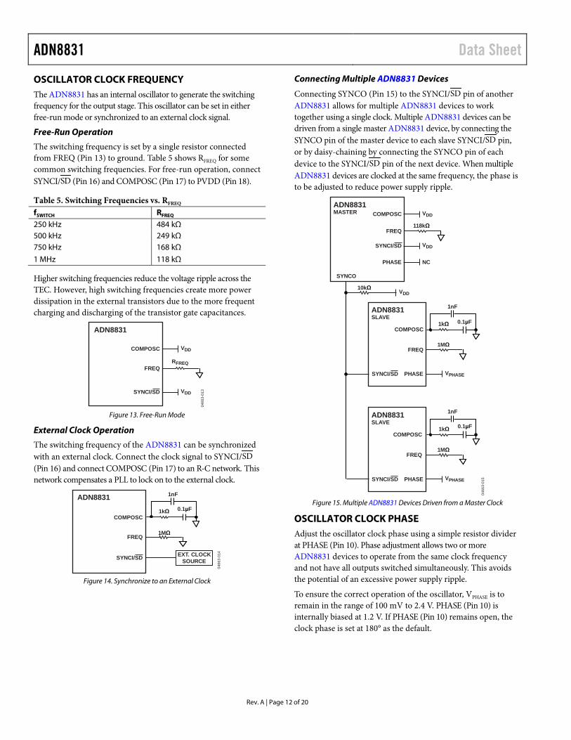
Connecting Multiple ADN8831 Devices
Connecting SYNCO (Pin 15) to the SYNCI/SD pin of another ADN8831 allows for multiple ADN8831 devices to work together using a single clock. Multiple ADN8831 devices can be driven from a single master ADN8831 device, by connecting the SYNCO pin of the master device to each slave SYNCI/SD pin, or by daisy-chaining by connecting the SYNCO pin of each device to the SYNCI/SD pin of the next device. When multiple ADN8831 devices are clocked at the same frequency, the phase is to be adjusted to reduce power supply ripple.
ADN8831MASTER COMPOSC
FREQ
SYNCI/SD
VDD
VDD
118kΩ
ADN8831SLAVE
COMPOSC
FREQ1MΩ
1kΩ 0.1µF
1nF
VPHASEPHASE
ADN8831SLAVE
COMPOSC
FREQ1MΩ
1kΩ 0.1µF
1nF
VPHASEPHASE
PHASE NC
10kΩVDD
0466
3-01
5
SYNCO
SYNCI/SD
SYNCI/SD
Figure 15. Multiple ADN8831 Devices Driven from a Master Clock
OSCILLATOR CLOCK PHASE Adjust the oscillator clock phase using a simple resistor divider at PHASE (Pin 10). Phase adjustment allows two or more ADN8831 devices to operate from the same clock frequency and not have all outputs switched simultaneously. This avoids the potential of an excessive power supply ripple.
To ensure the correct operation of the oscillator, VPHASE is to remain in the range of 100 mV to 2.4 V. PHASE (Pin 10) is internally biased at 1.2 V. If PHASE (Pin 10) remains open, the clock phase is set at 180° as the default.

Data Sheet ADN8831
Rev. A | Page 13 of 20
TEMPERATURE LOCK INDICATOR The TMPGD (Pin 11) outputs a logic high when the OUT1 (Pin 4) voltage reaches the IN2P (Pin 5) temperature setpoint (TEMPSET) voltage. The TMPGD has a detection range of ±25 mV and a 10 mV typical hysteresis. This allows direct interfacing either to the microcontrollers or to the supervisory circuitry.
SOFT START ON POWER-UP The ADN8831 can be programmed to ramp up for a specified time after the power supply is turned on or after the SD pin is deasserted. This feature, called soft start, is useful for gradually increasing the duty cycle of the PWM amplifier. The soft start time is set with a single capacitor connected from SS (Pin 14) to ground. The capacitor value is calculated by the following equation:
SSSS C×=τ 150
where: CSS is the value of the capacitor in microfarads. τSS is the soft start time in milliseconds.
To set a soft start time of 15 ms, CSS is to equal 0.1 μF.
SHUTDOWN MODE The shutdown mode sets the ADN8831 into an ultralow current state. The current draw in shutdown mode is typically 8 µA. The shutdown input, SD (Pin 16), is active low. To shut down the device, drive SD to logic low. Once a logic high is applied, the ADN8331 is reactivated after the time delay set by the soft start circuitry. Refer to the Soft Start on Power-Up section for more details.
STANDBY MODE The ADN8831 has a standby mode that deactivates a MOSFET driver stage. The current draw for the ADN8831 in standby mode is less than 2 mA. The standby input SS/SB (Pin 14) is active low. After applying a logic high, the ADN8331 reactivates following the delay. In standby mode, only SYNCO (Pin 15) has a clock output. All the other function blocks are powered off.
TEC VOLTAGE/CURRENT MONITOR The TEC real time voltage and current are detectable at VTEC (Pin 30) and ITEC (Pin 29), respectively.
Voltage Monitor
VTEC (Pin 30) is an analog voltage output pin with a voltage proportional to the actual voltage across the TEC. A center VTEC voltage of 1.25 V corresponds to 0 V across a TEC. The output voltage is calculated using the following equation:
)(25.0V25.1 SFBLFBVTEC VVV −×+=
Current Monitor
ITEC (Pin 29) is an analog voltage output pin with a voltage proportional to the actual current through the TEC. A center ITEC voltage of 1.25 V corresponds to 0 A through the TEC. The output voltage is calculated using the following equation:
)(25V25.1 CSLFBITEC VVV −×+= The equivalent TEC current is calculated using the following equation:
SENSE
ITECTEC R
VI
×
−=
25V25.1
MAXIMUM TEC VOLTAGE LIMIT The maximum TEC voltage is set by applying a voltage at VLIM (Pin 31) to protect the TEC. This voltage can be set with a resistor divider or a DAC. The voltage limiter operates in bidirectional TEC voltage, and cooling and heating voltage.
Using a DAC
Both the cooling and heating voltage limits are set at the same levels when a voltage source directly drives VLIM (Pin 31). The maximum TEC voltage is calculated using the following equation:
VLIMMAXTEC VV ×= 5)(
where: VTEC (MAX) is the maximum TEC voltage. VVLIM is the voltage applied at VLIM (Pin 31).
Using a Resistor Divider
Separate voltage limits are set using a resistor divider. The internal current sink circuitry connected to VLIM (Pin 31) draws a current when the ADN8831 drives the TEC in a heating direction, which lowers the voltage at VLIM (Pin 31). The current sink is not active when the TEC is driven in a cooling direction; therefore, the TEC heating voltage limit is always lower than the cooling voltage limit.
ADN8831VLIM
VLIM
FREQ
RA
RB
RFREQ
VREF
ISINK
0466
3-01
6
Figure 16. Using a Resistor Divider

ADN8831 Data Sheet
Rev. A | Page 14 of 20
The sink current is set by the resistor connected from FREQ (Pin 13) to ground. The sink current is calculated using the following equation:
FREQSINK R
IV25.1
=
where: ISINC is the sink current at VLIM (Pin 31). RFREQ is the resistor connected at FREQ (Pin 13).
The cooling and heating limits are calculated using the following equations:
BA
BREFCOOLVLIM RR
RVV
+×
=,
BASINKCOOLVLIMHEATVLIM RRIVV ×−= ,,
MAXIMUM TEC CURRENT LIMIT To protect the TEC, separate maximum TEC current limits in cooling and heating directions are set by applying a voltage at ILIMC (Pin 1) and ILIMH (Pin 32). Maximum TEC currents are calculated using the following equations:
SENSE
ILIMCCOOLMAXTEC R
VI
×−
=25
V25.1,,
SENSE
ILIMHHEATMAXTEC R
VI
×−
=25
V25.1,,

Data Sheet ADN8831
Rev. A | Page 15 of 20
APPLICATIONS INFORMATION
0466
3-01
7
Chop1–
+
Chop2–
+IN1P IN2P
IN2NIN1NOUT1 OUT2
17.68kΩ
7.68kΩ RXRFB
RTH
(10kΩ @ 25°C)
VREF
VREF/2R
7432
VTEMPSET
5 6
VOUT1 VOUT2
Z1 Z2
TEC
LPF
SFB
SPGATE
SNGATE
LPGATE
LNGATE
LFB
PWM
LINEAR
THERMISTOR INPUTAMPLIFIERAV = RFB/(RTH + RX) – RFB/R
PID COMPENSATORAMPLIFIERAV = Z2/Z1
MOSFET DRIVERAV = 5
CONTROL
Figure 17. Signal Flow Block Diagram
SIGNAL FLOW The ADN8831 integrates two auto-zero amplifiers defined as the Chop1 amplifier and the Chop2 amplifier. Both of the amplifiers can be used as standalone amplifiers, therefore, the implementation of temperature control can vary. Figure 17 shows the signal flow through the ADN8831, and a typical implementation of the temperature control loop using the Chop1 amplifier and the Chop2 amplifier.
In Figure 17, the Chop1 amplifier and the Chop2 amplifier are configured as the thermistor input amplifier and the PID compensation amplifier, respectively. The thermistor input amplifier gains the thermistor voltage then outputs to the PID compensation amplifier. The PID compensation amplifier then compensates a loop response over the frequency domain.
The output from the compensation loop at OUT2 is fed to the linear MOSFET gate driver. The voltage at LFB is fed with OUT2 into the PWM MOSFET gate driver. Including the external transistors, the gain of the differential output section is fixed at 5. For details on the output drivers, see the MOSFET Driver Amplifier section.
THERMISTOR SETUP The thermistor has a nonlinear relationship to temperature; near optimal linearity over a specified temperature range can be achieved with the proper value of RX placed in series with the thermistor. First, the resistance of the thermistor must be known, where
HIGHTHHIGH
MIDTHMID
LOWTHLOW
TRRTRRTRR
@@@
=
=
=
TLOW and THIGH are the endpoints of the temperature range and TMID is the average. In some cases, with only B constant available , RTH is calculated using the following equation:
−=
RRTH TT
BRR 11exp
where: RTH is a resistance at T[K]. RR is a resistance at TR[K].
RX is calculated using the following equation:
−+−+
=MIDHIGHLOW
HIGHLOWHIGHMIDMIDLOWX RRR
RRRRRRR
22
THERMISTOR AMPLIFIER (Chop1) The Chop1 amplifier can be used as a thermistor input amplifier. In Figure 17, the output voltage is a function of the thermistor temperature. The voltage at OUT1 is expressed as
21 REFFB
XTH
FBOUT1
VR
RRR
RV ×
+−
+=
where: RTH is a thermistor. RX is a compensation resistor.
R is calculated using the following equation:
CTHX RRR °+= 25@
VOUT1 is centered around VREF/2 at 25°C. With the typical values shown in Figure 17, an average temperature-to-voltage coefficient is −25 mV/°C at a range of +5°C to +45°C.

ADN8831 Data Sheet
Rev. A | Page 16 of 20
0466
3-01
8
–15 5 25 450
2.5
65
0.5
1.0
1.5
2.0
TEMPERATURE(°C)
VO
UT
1 (
V)
Figure 18. VOUT1 vs. Temperature
PID COMPENSATION AMPLIFIER (Chop2) Use the Chop2 amplifier as the PID compensation amplifier. The voltage at OUT1 feeds into the PID compensation amplifier. The frequency response of the PID compensation amplifier is dictated by the compensation network. Apply the temperature set voltage at IN2P. In Figure 17, the voltage at OUT2 is calcu-lated using the following equation:
)( TEMPSETOUT1TEMPSETOUT2 VVZ1Z2
VV
The user sets the exact compensation network. This network varies from a simple integrator to PI, PID, or any other type of network. The user also determines the type of compensation and component values because they are dependent on the thermal response of the object and the TEC. One method for empirically determining these values is to input a step function to IN2P, therefore changing the target temperature, and adjusting the compensation network to minimize the settling time of the TEC temperature.
A typical compensation network for temperature control of a laser module is a PID loop consisting of a very low frequency pole and two separate zeros at higher frequencies. Figure 19 shows a simple network for implementing PID compensation. To reduce the noise sensitivity of the control loop, an additional pole is added at a higher frequency than the zeros. The bode plot of the magnitude is shown in Figure 20. The unity-gain crossover frequency of the feedforward amplifier is calculated using the following equation:
TECGAINR3C1
f
802
1dB0
To ensure stability, the unity-gain crossover frequency is to be lower than the thermal time constant of the TEC and thermistor. However, this thermal time constant is sometimes unspecified making it difficult to characterize. There are many texts written on loop stabilization, and it is beyond the scope of this data sheet to discuss all methods and trade offs in optimizing compensation networks.
ADN8831
CHOP2–
+
IN2P IN2N4 76
OUT1 OUT25
C1
CFC2R2
R3
VTEMPSET
R1
0466
3-01
9
Figure 19. Implementing a PID Compensation Loop
0466
3-02
0
FREQUENCY (Hz Log Scale)
MA
GN
ITU
DE
(L
og
Sca
le)
0dB
12πR3C1
R1R3
12πR3C2
12πR1C1
12πC2 (R2 + R3)
R1R2 || R3
Figure 20. Bode Plot for PID Compensation
With an ADN8831-EVALZ board, AN-695, an application note shows how to determine the PID network components for a stable TEC subsystem performance.

Data Sheet ADN8831
Rev. A | Page 17 of 20
MOSFET DRIVER AMPLIFIER The ADN8831 has two separate MOSFET drivers: a switched output or pulse-width modulated (PWM) amplifier, and a high gain linear amplifier. Each amplifier has a pair of outputs that drive the gates of external MOSFETs which, in turn, drive the TEC as shown in Figure 17. A voltage across the TEC is monitored via SFB (Pin 23) and LFB (Pin 27). Although both MOSFET drivers achieve the same result, to provide constant voltage and high current, their operation is different. The exact equations for the two outputs are
)25.1(40 −−= OUT2BLFB VVV
)25.1(5 −+= OUT2LFBSFB VVV
where: VOUT2 is the voltage at OUT2 (Pin 7). VB is determined by VDD as
]V0.4[V5.1 <= DDB VV
]V0.4[V5.2 >= DDB VV
The voltage at OUT2 (Pin 7) is determined by the compensation network that receives temperature set voltage and thermistor voltage fed by the input amplifier. VLFB has a low limit of 0 V and an upper limit of VDD. Figure 21 shows the graphs of these equations.
0
2.5
5.0
LFB
(V)
0
2.5
5.0
SFB
(V)
–5.0
–2.5
0
2.5
5.0
0 0.25 0.75 1.25 1.75 2.25 2.75
VTEC
(V)
LFB
-SFB
0466
3-02
1
OUT2 (V) Figure 21. OUT2 Voltage vs. TEC Voltage

ADN8831 Data Sheet
Rev. A | Page 18 of 20
OUTLINE DIMENSIONS
COMPLIANT TO JEDEC STANDARDS MO-220-WHHD. 1124
08-A
10.50BSC
BOTTOM VIEWTOP VIEW
PIN 1INDICATOR
32
916
17
24
25
8
EXPOSEDPAD
PIN 1INDICATOR
3.253.10 SQ2.95
SEATINGPLANE
0.05 MAX0.02 NOM
0.20 REF
COPLANARITY0.08
0.300.250.18
5.105.00 SQ4.90
0.800.750.70
FOR PROPER CONNECTION OFTHE EXPOSED PAD, REFER TOTHE PIN CONFIGURATION ANDFUNCTION DESCRIPTIONSSECTION OF THIS DATA SHEET.
0.500.400.30
0.25 MIN
Figure 22. 32-Lead Lead Frame Chip Scale Package [LFCSP_VQ]
5 mm× 5 mm Body, Very Thin Quad (CP-32-7)
Dimensions Shown in Millimeters
ORDERING GUIDE Model1 Temperature Range Package Description Package Option ADN8831ACPZ-R2 −40C to +85C 32-Lead Lead Frame Chip Scale Package [LFCSP_VQ] CP-32-7
ADN8831ACPZ-REEL7 −40C to +85C 32-Lead Lead Frame Chip Scale Package [LFCSP_VQ] CP-32-7
ADN8831-EVALZ −40C to +85C Evaluation Board 1 Z = RoHS Compliant Part.

Data Sheet ADN8831
Rev. A | Page 19 of 20
NOTES

ADN8831 Data Sheet
Rev. A | Page 20 of 20
NOTES
©2005–2012 Analog Devices, Inc. All rights reserved. Trademarks and registered trademarks are the property of their respective owners. D04663-0-8/12(A)