thermoelectric properties of ultrascaled silicon...
TRANSCRIPT
THERMOELECTRIC PROPERTIES OF ULTRASCALED SILICON NANOWIRES
by
Edwin Bosco Ramayya
A dissertation submitted in partial fulfillment of
the requirements for the degree of
Doctor of Philosophy
(Electrical Engineering)
at the
UNIVERSITY OF WISCONSIN–MADISON
2010

c© Copyright by Edwin Bosco Ramayya 2010
All Rights Reserved
iv
TABLE OF CONTENTS
Page
LIST OF TABLES . . . . . . . . . . . . . . . . . . . . . . . . . . . . . . . . . . . . . . . vi
LIST OF FIGURES . . . . . . . . . . . . . . . . . . . . . . . . . . . . . . . . . . . . . . vii
ABSTRACT . . . . . . . . . . . . . . . . . . . . . . . . . . . . . . . . . . . . . . . . . . xiv
1 Introduction . . . . . . . . . . . . . . . . . . . . . . . . . . . . . . . . . . . . . . . . 1
1.1 Thermoelectric Effects . . . . . . . . . . . . . . . . . . . . . . . . . . . . . . . . 21.2 Figure Of Merit For Thermoelectric Cooling . . . . . . . . . . . . . . . . . . . . . 41.3 Semiconductors in Thermoelectric Applications . . . . . . . . . . . . . . . . . . . 81.4 Motivation for this Work . . . . . . . . . . . . . . . . . . . . . . . . . . . . . . . 91.5 Aims of this Work . . . . . . . . . . . . . . . . . . . . . . . . . . . . . . . . . . . 12
1.5.1 Electron Transport Simulator . . . . . . . . . . . . . . . . . . . . . . . . . 121.5.2 Phonon Transport Simulator . . . . . . . . . . . . . . . . . . . . . . . . . 131.5.3 Thermoelectric Simulator . . . . . . . . . . . . . . . . . . . . . . . . . . 13
2 Electronic Transport in Silicon Nanowires . . . . . . . . . . . . . . . . . . . . . . . 15
2.1 Historical Overview . . . . . . . . . . . . . . . . . . . . . . . . . . . . . . . . . . 152.1.1 Electronic Bandstructure Modification in Nanowires . . . . . . . . . . . . 162.1.2 Acoustic Phonon Confinement in Nanowires . . . . . . . . . . . . . . . . 19
2.2 Preliminary Research : Electron Mobility in SiNWs . . . . . . . . . . . . . . . . . 202.2.1 Introduction and Motivation . . . . . . . . . . . . . . . . . . . . . . . . . 212.2.2 Device Structure and Simulator Components . . . . . . . . . . . . . . . . 232.2.3 Scattering due to Bulk Acoustic Phonons, Intervalley Phonons, and Sur-
face Roughness . . . . . . . . . . . . . . . . . . . . . . . . . . . . . . . . 252.2.4 Effect of Decreasing Channel Width on Mobility . . . . . . . . . . . . . . 272.2.5 Acoustic Phonon Confinement . . . . . . . . . . . . . . . . . . . . . . . . 312.2.6 Electron Mobility in SiNWs Revisited: The role of acoustic phonon con-
finement and surface roughness scattering . . . . . . . . . . . . . . . . . . 352.3 Conclusion . . . . . . . . . . . . . . . . . . . . . . . . . . . . . . . . . . . . . . 40

v
Page
3 Thermoelectric Figure of Merit . . . . . . . . . . . . . . . . . . . . . . . . . . . . . 42
3.1 Derivation of Electronic Coefficients in ZT . . . . . . . . . . . . . . . . . . . . . 423.2 Electrical Conductivity . . . . . . . . . . . . . . . . . . . . . . . . . . . . . . . . 443.3 Lattice Thermal Conductivity . . . . . . . . . . . . . . . . . . . . . . . . . . . . . 47
3.3.1 Lattice Thermal Conductivity Using the Klemens-Callaway Method . . . . 493.3.2 Lattice Thermal Conductivity from 1D BTE . . . . . . . . . . . . . . . . . 513.3.3 Thermal Conductivity Using the Monte Carlo Method . . . . . . . . . . . 53
3.4 Electronic Thermal Conductivity . . . . . . . . . . . . . . . . . . . . . . . . . . . 603.5 The Seebeck Coefficient . . . . . . . . . . . . . . . . . . . . . . . . . . . . . . . 61
3.5.1 Electronic Seebeck Coefficient . . . . . . . . . . . . . . . . . . . . . . . . 613.5.2 Phononic Seebeck Coefficient : Phonon Drag . . . . . . . . . . . . . . . . 61
3.6 ZT Dependence on the Silicon Nanowire Cross Section . . . . . . . . . . . . . . . 633.7 Conclusion . . . . . . . . . . . . . . . . . . . . . . . . . . . . . . . . . . . . . . 65
4 Summary and Future Work . . . . . . . . . . . . . . . . . . . . . . . . . . . . . . . 66
4.1 Summary . . . . . . . . . . . . . . . . . . . . . . . . . . . . . . . . . . . . . . . 664.2 Future Work . . . . . . . . . . . . . . . . . . . . . . . . . . . . . . . . . . . . . . 68
4.2.1 Lattice Thermal Conductivity Modeling . . . . . . . . . . . . . . . . . . . 694.2.2 Density of States Broadening . . . . . . . . . . . . . . . . . . . . . . . . . 70
LIST OF REFERENCES . . . . . . . . . . . . . . . . . . . . . . . . . . . . . . . . . . . 71
APPENDICES
Appendix A: Calculation of Electron Scattering Rates . . . . . . . . . . . . . . . . . 78Appendix B: Self-consistent Poisson-Schrodinger-Monte Carlo Solver . . . . . . . . 89Appendix C: Ensemble Monte Carlo Solver for Acoustic Phonon Transport . . . . . . 98

DISCARD THIS PAGE
vii
LIST OF FIGURES
Figure Page
1.1 Schematic to illustrate the Seebeck effect. A temperature gradient across the lengthof an open-circuited semiconductor results in a voltage V across it. . . . . . . . . . . 3
1.2 Schematic to illustrate the Peltier effect. A current through the semiconductor resultsin removal of heat at contact #1 and heating at contact #2 due to the difference in theheat carried by the carriers in different materials. . . . . . . . . . . . . . . . . . . . . 4
1.3 Schematic of thermocouples used in thermoelectric (Peltier) coolers (left) and powergenerators (right). Thermoelectric devices are generally made of several thermocou-ples connected in parallel. The two legs of the couple are electrically in series butthermally in parallel. . . . . . . . . . . . . . . . . . . . . . . . . . . . . . . . . . . . 5
1.4 Variation of electrical and thermal conductivity, the Seebeck coefficient, and the ther-moelectric figure of merit in insulators, semiconductors, and metals. ZT is found tobe maximum in semiconductors. . . . . . . . . . . . . . . . . . . . . . . . . . . . . . 8
1.5 History of thermoelectric figure of merit, ZT , at 300 K. Since the discovery of thethermoelectric properties of Bi2Te3 and its alloys with Sb and Se in the 1950s, nobulk material with ZT300K > 1 has been discovered. Recent studies in nanostructuredthermoelectric materials have led to a sudden increase in ZT300K > 1 [1]. . . . . . . . 10
2.1 Crystal structure of an idealized silicon NW. The NW unit cell is shown on the right.Each base unit contains four atoms. The faces are parallel to the four equivalent 110planes and the wire is oriented along [001]. . . . . . . . . . . . . . . . . . . . . . . . 17
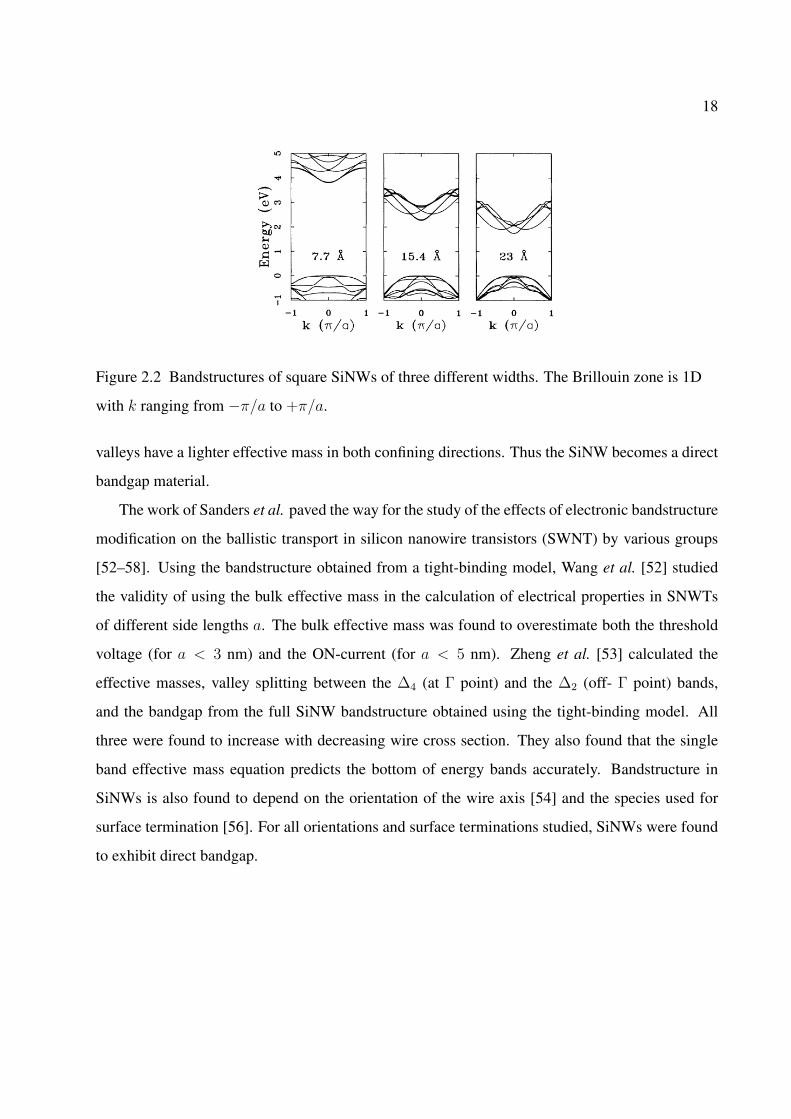
2.2 Bandstructures of square SiNWs of three different widths. The Brillouin zone is 1Dwith k ranging from −π/a to +π/a. . . . . . . . . . . . . . . . . . . . . . . . . . . . 18
viii
Figure Page
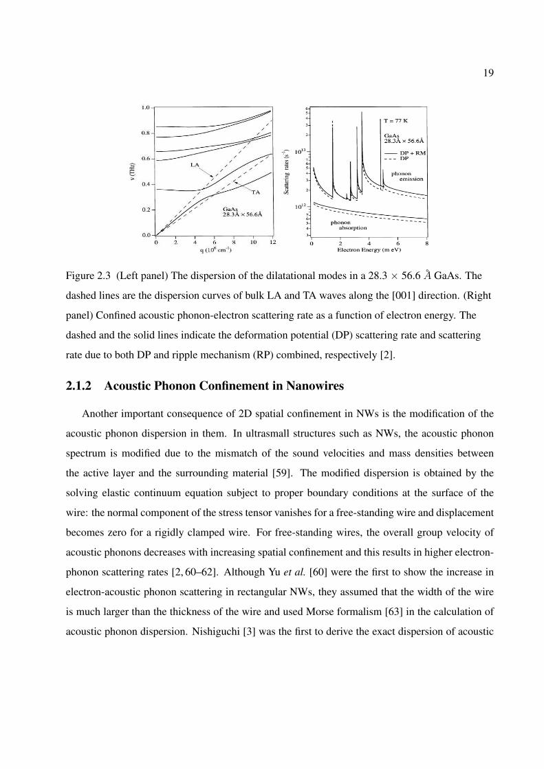
2.3 (Left panel) The dispersion of the dilatational modes in a 28.3 × 56.6 A GaAs. Thedashed lines are the dispersion curves of bulk LA and TA waves along the [001] di-rection. (Right panel) Confined acoustic phonon-electron scattering rate as a functionof electron energy. The dashed and the solid lines indicate the deformation potential(DP) scattering rate and scattering rate due to both DP and ripple mechanism (RP)combined, respectively [2]. . . . . . . . . . . . . . . . . . . . . . . . . . . . . . . . . 19
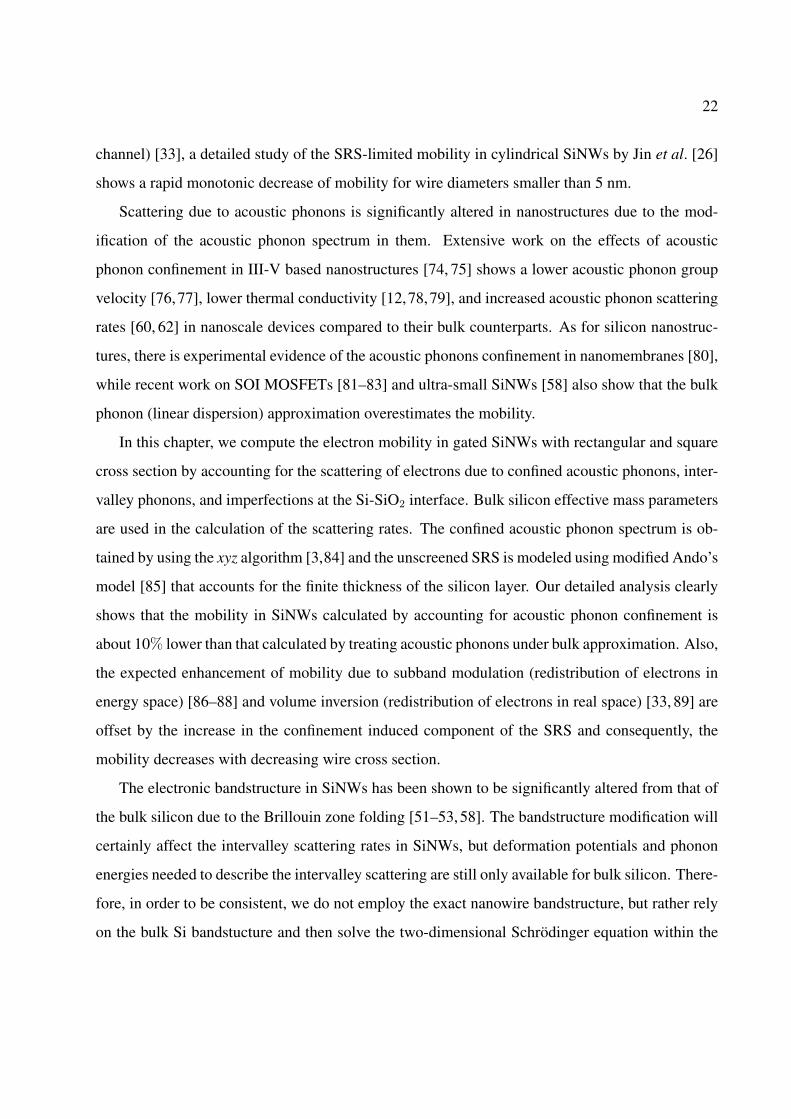
2.4 Schematic of the simulated 8×8 nm2 SiNW on ultrathin SOI. . . . . . . . . . . . . . 23
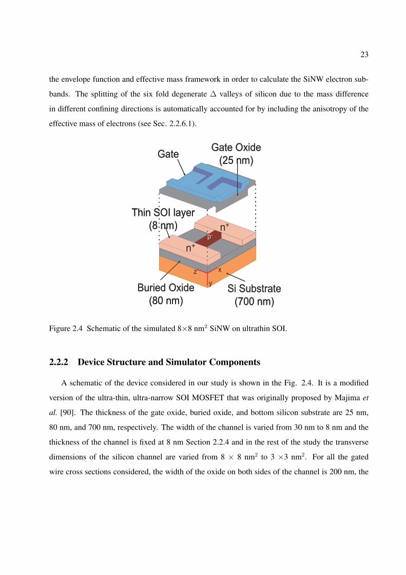
2.5 Flowchart of the simulator developed to calculate the electron mobility in SiNWs. . . 24
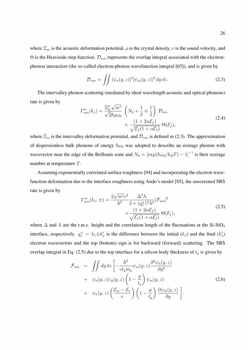
2.6 Variation of the field-dependent mobility with varying SiNW width. The wire thick-ness is kept constant at 8 nm. . . . . . . . . . . . . . . . . . . . . . . . . . . . . . . . 28
2.7 Variation of the overlap integral for the lowest subband with varying wire width, ob-tained from (2.3) at a constant sheet density of Ns = 2.9× 1011cm−2. . . . . . . . . . 29
2.8 Variation of the average distance of carriers from the top interface (below the gate) forvarious wire widths as a function of the effective transverse field. . . . . . . . . . . . 30
2.9 Electron distribution across the nanowire, for the wire width of 30 nm (left panel) and8 nm (right panel). In both panels, the transverse field is 1 MV/cm, the wire thicknessis 8 nm, and the color scale is in ×1019cm−3. . . . . . . . . . . . . . . . . . . . . . . 30
2.10 Confined acoustic phonon dispersion (dilatational mode) calculated using the xyz al-gorithm [3] for an 8× 8 nm2 SiNW. Only the lowest 10 phononic subbands are shown.Dispersion in the first one third of the first Brillouin zone is shown for clarity. . . . . . 31
2.11 Electron-acoustic phonon scattering rate of an 8 × 8 nm2 SiNW at the channel sheetdensity of Ns = 8.1× 1011 cm−2, calculated assuming the bulk and confined phononapproximations. The electron-bulk acoustic phonon intersubband spikes are at around20 meV, 52 meV, 85 meV, and 95 meV and they correspond to the electron scatteringfrom the lowest subband to the 2nd, 3rd, 4th, and the 5th lowest subbands. The set ofspikes indicated by Ab and Em correspond to the absorption and emission of phononsfrom different phonon subbands. . . . . . . . . . . . . . . . . . . . . . . . . . . . . . 34
2.12 Variation of the field-dependent mobility for an 8 × 8 nm2 SiNW assuming bulkacoustic phonons (solid line) and confined acoustic phonons (dashed line). . . . . . . 36
2.13 Variation of the electron mobility with SiNW cross section at three different transversefields. . . . . . . . . . . . . . . . . . . . . . . . . . . . . . . . . . . . . . . . . . . . 37
ix
Figure Page
2.14 Variation of the electron population at a low transverse field (1.4×10⁻² MV/cm). Thesolid line shows the total population of the electrons in the lowest subband in each ofthe four ∆4 valley pairs and the dashed line shows population of the ∆2 valley pair,with varying spatial confinement. . . . . . . . . . . . . . . . . . . . . . . . . . . . . 38
2.15 Electron density across the nanowire at a high transverse field (1.04 MV/cm). Whenthe cross section is reduced from 8 × 8 nm2 (bottom right panel) to 3 × 3 nm2 (topleft), the onset of volume inversion is evident. The color scale is in 5 ×1018 cm−3. . . 39
2.16 Variation of the electron-phonon overlap with SiNW cross section at a low transversefield (1.4 ×10⁻² MV/cm). This results in a fourfold increase in the intrasubbandphonon scattering rates, as the thickness and width of square wires are varied from 8nm to 3 nm. . . . . . . . . . . . . . . . . . . . . . . . . . . . . . . . . . . . . . . . . 40
3.1 Cross section of an ungated SiNW surrounded by thermal oxide. The wire is doped to1.6 × 1019 cm−3 with arsenic. . . . . . . . . . . . . . . . . . . . . . . . . . . . . . . 45
3.2 Electrical conductivity in square SiNWs as a function of the wire cross section fordifferent interface roughnesses. The rapid drop in conductivity for wires of crosssection below 5 × 5 nm2 is because of a significant increase in surface roughnessscattering in ultra-small wires. The conductivity decreases with increase in the rms ofthe roughness at the Si/SiO2 interface. . . . . . . . . . . . . . . . . . . . . . . . . . . 46
3.3 Thermal simulator flowchart developed to solve the phonon Boltzmann equation. . . . 49
3.4 Group velocity of dilatational modes for an 8 x 8 nm2 SiNW. On average, acousticphonon group velocity is reduced to less than 50 % of the bulk value (9.13 x 105 cm/s). 50
3.5 Phononic component of thermal conductivity as a function of the SiNW cross sectioncalculated assuming completely diffuse scattering at the boundaries. (red solid line)κl calculated from Klemens-Callaway’s expression. (blue dotted line with circles)κl calculated from the 1D phonon BTE. κl rolls off for larger wires because morephononic bands are needed; the κl extrapolated from smaller cross section is shownin black solid line. Thermal conductivity in SiNWs is almost two orders of magnitudesmaller than that in bulk silicon because of strong phonon-boundary scattering. Notethat this is true only in the limit of complete diffuse scattering at the boundaries (whichcorresponds to boundary rms roughness of about ∆ = 3 nm [4]). . . . . . . . . . . . . 51
x
Figure Page
3.6 (left panel) The exponentially correlated surface generated using FFT for ∆ = 0.3 nmand Λ = 2.5 nm. (right panel) A sample trajectory of showing a phonon hitting thesurface and spending sometime before getting out. . . . . . . . . . . . . . . . . . . . 54
3.7 Schematic of a nanowire showing, the initial distribution of phonons: red and bluedots indicate phonons at temperature 310 K and 290 K, respectively. . . . . . . . . . . 56
3.8 Transient temperature profile along the length of the wire for ballistic and diffusephonon transport. (left panel) For the ballistic case, in steady state, the temperatureis constant along the wire with discontinuities at the two end cells. (right panel) Indiffusive transport, a linear temperature profile is established along the wire when thesystem reaches steady state. The time taken to reach a steady state increases with theincrease in the length of the wire. The length of the wire in the left and the right panelare 4 µm and 200 nm, respectively. . . . . . . . . . . . . . . . . . . . . . . . . . . . 57
3.9 Phononic contribution to the thermal conductivity as a function of the SiNW cross sec-tion for two different roughness at Si/SiO2 interface. Thermal conductivity in SiNWsis more than an order of magnitude smaller than that in bulk silicon because of strongphonon-boundary scattering. . . . . . . . . . . . . . . . . . . . . . . . . . . . . . . . 59
3.10 Electronic contribution to thermal conductivity as a function of the SiNW cross sec-tion for different roughness at Si/SiO2 interface. κe follows the same trend as σ vari-ation with cross section and roughness. As in bulk silicon, κe is smaller than κl. . . . . 60
3.11 Electronic (left) and phonon-drag (right) components of the Seebeck coefficient asa function of the SiNW cross section and rms of surface roughness. The electroniccomponent of the Seebeck coefficient is more than an order of magnitude greaterthan the phonon-drag component. Phonon drag component decreases with increasingroughness at the interface, because of the decrease in the mean free path of phonons. . 62
3.12 The flowchart of the electrothermal simulator used to calculate the ZT of SiNWs. . . . 64
3.13 ZT variation with the nanowire cross section. In extremely thin wires, contrary toconventional belief, decreasing the cross section does not result in an exponential in-crease in ZT because of the rapid decrease in electrical conductivity owing to strongelectron-surface roughness scattering. ZT obtained assuming complete diffuse bound-ary scattering for phonons (red) is definitely an overestimation. ZT obtained using theactual surface defined by rms = 0.25 nm in phonon Monte Carlo (blue). Predictionfrom Hicks and Dresselhauss [5], showing exponential increase in ZT with decreasingwire cross section (black). . . . . . . . . . . . . . . . . . . . . . . . . . . . . . . . . 64
xi
Figure Page
4.1 Variation of the power factor with doping density for a 5 nm× 5 nm silicon nanowire.There is an optimal doping density for which the power factor is maximal whichdepends on the wire cross section and the rms roughness of the wire. . . . . . . . . . . 68
4.2 Density of states of a 5 nm × 5 nm SiNW (black) and effect of two levels of surfaceroughness, 0.14 nm (red) and 0.4 nm (magenta). Roughness smears the high peaksin the DOS, negating potential benefits that quantum confinement could have on theSeebeck coefficient. . . . . . . . . . . . . . . . . . . . . . . . . . . . . . . . . . . . 70
B.1 Flowchart for the Self-consistent Poisson-Schrodinger solver. . . . . . . . . . . . . . 91
B.2 Results from the Poisson-Schrodinger-Monte Carlo Solver. (top panel) The potentialprofile along the y direction (top left) and the z direction (top right) obtained from theself-consistent Poisson-Schrodinger solver. (bottom panel) Variation of the electronenergy (left) and velocity (right) with time from the EMC. Steady state (indicated bysaturation of energy and velocity) is reached on picosecond timescales.. . . . . . . . . 93
B.3 Flight dynamics of the ensemble Monte Carlo method. The horizontal lines show thetrajectories of particles 1 through N along the time axis, and each star-like symbol onthe horizontal line represents a scattering event. The vertical dotted lines indicate thesampling times, spaced by dt, at which the electron distribution function f is evaluatedfrom the ensemble. . . . . . . . . . . . . . . . . . . . . . . . . . . . . . . . . . . . . 95
B.4 Flowchart of the ensemble Monte Carlo transport kernel. . . . . . . . . . . . . . . . 97
C.1 (top) Normal three-phonon scattering: two phonons with wavevectors K1 and K2
interact to give the third phonon of wavevector K3 and vice versa. In this case thenet momentum of the phonon system is unaltered. Although this type of scatteringdoes not pose any resistance to the heat flow directly, it can not be ignored, becauseit changes the distribution of phonons thereby increasing or decreasing the umklappthree phonon scattering. (bottom) Umklapp three-phonon scattering: two phononswith wavevectors K1 and K2 interact to give the third phonon of wavevector K3. Inthis case the momentum is conserved up to an integer multiple of the inverse latticevector G. This directly poses resistance to heat flow because it can reverse/change thedirection of the heat flow. . . . . . . . . . . . . . . . . . . . . . . . . . . . . . . . . . 99
C.2 Acoustic phonon dispersion for LA and TA phonons in silicon in the fist Brillouinzone obtained using a quadratic fit of the experimental data [6]. . . . . . . . . . . . . 102
xii
Figure Page
C.3 Transient temperature profile along the length of the wire for diffuse phonon trans-port.In diffuse transport, a linear temperature profile is established along the length ofthe wire when the system reaches steady state. The time taken to reach a steady stateincreases with the increase in the length of the wire. . . . . . . . . . . . . . . . . . . 104
C.4 The steady state temperature profile along the wire (left panel). Only phonon-phononscattering is considered. In the case of diffuse scattering, the steady state profile islinear along the wire. The transient energy of all the phonons in the wire (right panel).The energy of the system increases with time and saturates as the system reaches thesteady state indicated by a linear temperature profile. . . . . . . . . . . . . . . . . . . 104
C.5 The steady state temperature profile along the wire (left panel). Only phonon-phononscattering is considered. In the case of diffuse scattering, the steady state profile islinear along the wire. In this case TH = 85 K and TL = 75 K. The mean free path ofphonons in this case is few microns, therefore, we can see discontinuity in temperatureat the two end cells and linear profile inside the wire signifying quasi-ballistic phonontransport. The transient energy of all the phonons in the wire (right panel). The energyof the system increases with time and saturates as the system reaches the steady stateindicated by a linear temperature profile along the wire. . . . . . . . . . . . . . . . . . 105
C.6 The steady state temperature profile along the wire (left panel). phonon-phonon +boundary-phonon scattering are considered. In the case of diffuse scattering, thesteady state profile should be linear along the wire but it clearly is not linear. Thetransient energy of all the phonons in the wire (right panel). The energy of the sys-tem should increase with time, but it decreases and saturates in steady state. Thisis because of incorrect randomization of phonons at the boundaries which results inincrease in flux leaving the wire. . . . . . . . . . . . . . . . . . . . . . . . . . . . . . 108
C.7 The steady state temperature profile along the wire (left panel). 10 × phonon-phonon+ boundary-phonon scattering are considered. In the case of diffuse scattering, thesteady state profile should be linear along the wire but it clearly is not linear. Theprofile is more linear in the wire compared to the case with less phonon-phonon scat-tering. The transient energy of all the phonons in the wire (right panel). The energy ofthe system now increases with time but it saturates at a level lower than where it should[see Fig. C.4]. More phonon scattering tries to bring back the phonon distribution towhat it should be, therefore we get a better result in this case. . . . . . . . . . . . . . . 108
xiii
Figure Page
C.8 The steady state temperature profile along the wire (left panel). Only boundary-phonon scattering are considered. In the case of diffuse scattering, the steady stateprofile should be linear along the wire but it is parabolic. The transient energy ofall the phonons in the wire (right panel). The energy of the system should increasewith time, but it decreases and saturates in steady state. This is because of incorrectrandomization of phonons at the boundaries. . . . . . . . . . . . . . . . . . . . . . . 109
C.9 Variation of the average |q| of phonons in a cell with time. As more and more phononsundergo boundary scattering, the average qz component increases at the expense of theother two. Therefore the flux leaving the wire will be more than that injected into it.This is the reason for the fall in temperature inside the wire when boundary scatteringis introduced in our simulation [see Fig.(C.6)] . . . . . . . . . . . . . . . . . . . . . . 109
xiv
ABSTRACT
Thermoelectric devices convert heat to electricity or electricity to heat. The efficiency of ther-
moelectric (TE) devices is quantified by an unitless quantity called the thermoelectric figure of
merit, ZT = S2σT/κ, where S, σ, and κ are the Seebeck coefficient, electrical conductivity, and
thermal conductivity, respectively, and T is the operating temperature. For a material to be con-
sidered for TE applications, ZT should be at least 1. Bulk silicon has a ZT of about 0.01 and is
typically not a good candidate for TE conversion. ZT in silicon nanowires (SiNWs) of cross section
50 nm × 50 nm has been experimentally shown to be almost two orders of magnitude larger than
that of bulk silicon, opening up the possibility of all-silicon on-chip cooling. The ZT increase in
SiNWs is attributed to two orders of magnitude reduction in κ because of severe phonon-boundary
scattering. It is also believed that the power factor (S2σ) can be increased by decreasing the wire
cross section further, opening up the possibility of achieving ZT > 1 in ultrascaled SiNWs. In
this work, the room-temperature ZT of highly doped ultrascaled silicon nanowires of square cross
section (3 nm × 3 nm to 8 nm × 8 nm) is calculated by solving the electron and phonon Boltz-
mann transport equations (BTE) with a proper account of the two dimensional confinement of both
electrons and phonons.
The electronic part of the simulator developed has two components: the first is a self-consistent
2D Poisson-2D Schrodinger solver and the second is an electron ensemble Monte-Carlo (EMC)
transport kernel. The former is used to calculate the electronic states and the self-consistent po-
tential distribution across the wire and the latter simulates electron transport along the axis of the
wire under the influence of the confining potential in the transverse directions and a very small
xv
lateral electric field along the wire. The scattering of electrons due to acoustic phonons, inter-
valley phonons, ionized impurities, and the imperfections (roughness) at the Si-SiO2 interface are
included in the EMC transport kernel. The roughness is described by an exponentially varying au-
tocorrelation function with rms ∆ and correlation length Λ. The electronic simulator calculates the
electrical conductivity as well as the electronic components of the Seebeck coefficient and thermal
conductivity.
The lattice thermal conductivity is calculated from the thermal simulator which solves the
acoustic phonon BTE using the Monte Carlo technique. The full dispersion of acoustic phonons
is used in the phonon EMC transport kernel. The surface of SiNW used in the phonon EMC is
generated using a Fast Fourier Transform (FFT) technique from a given autocorrelation function.
Phonon scattering with impurites, other phonons (both normal and umklapp 3-phonon processes),
and the boundaries of the wire are included in the phonon EMC to describe the phonon transport in
SiNWs accurately. Apart from the lattice thermal conductivity, the thermal simulator is also used
to calculate the acoustic phonon mean free path, which is then used to calculate the phonon drag
component of the Seebeck coefficient.
The electrical conductivity decreases with deceasing wire cross section because of the strong
increase in the electron surface roughness scattering and phonon scattering. With increasing con-
finement, the energy separation between the conduction band edge (EC) and the Fermi level (EF )
increases, which results in an increase in the average energy carried by electrons, therefore the
Seebeck coefficient increases as the wire cross section decreases. The power factor does not show
an exponential increase with decreasing wire cross section as predicted in earlier theoretical stud-
ies because the electrical conductivity there is almost 6-fold decrease in σ and less than 2-fold
increase in the Seebeck coefficient when the wire cross section is decreased from 8 nm × 8 nm to
3 nm × 3 nm. The thermal conductivity decreases with decreasing wire cross section because of
the increase in phonon-boundary scattering. For the roughness parameters considered (∆ = 0.25
nm and Λ = 2.5 nm), the lattice thermal conductivity is about 25-75 times smaller (depending on
the wire cross section) than that of bulk silicon. The phonon drag component of the Seebeck coef-
ficient is negligibly small in SiNWs because of a strong reduction in the phonon mean free path.
xvi
Also, as in bulk silicon, the electronic contribution to thermal conductivity is more than an order
of magnitude smaller than the contribution from phonons.
The ZT in SiNWs calculated from the themoelectric simulator is about 30 times larger than
that in bulk silicon: the enhancement in ZT occurs primarily because of the decrease in the lattice
thermal conductivity due to strong phonon-boundary scattering and not due to an enhancement in
the power factor. ZT does not increase drastically with decreasing wire cross as predicted by ear-
lier studies, because in ultra-narrow wires, roughening (apart from degrading thermal conductivity)
severely degrades electrical conductivity. It is extremely important to account for the actual rough
surface when solving the electron and phonon BTE in order to estimate ZT in nanostructures.

1
Chapter 1
Introduction
Thermoelectric phenomena include conversion of electricity to heat and heat to electricity using
solid state devices. A thermoelectric (TE) generator converts a temperature difference between
two ends of a conductor to a bias voltage, whereas a TE refrigerator utilizes electrical current
to create a temperature difference between two ends of a conductor, by pumping heat from cold
end to hot end. TE devices have attracted much attention among researchers because they do not
have any moving parts or fluids [liquids or gases like chloroflurocarbons (CFCs) that are used in
conventional refrigerators]. Most of the failures in conventional generators and refrigerators [7]
arise due to the failure of moving parts or fluid leaks. The absence of moving parts and fluids
make TE devices very reliable. Unlike conventional refrigerators, which pollute the atmosphere
because of CFC leaks, TE coolers are environmentally friendly. But TE devices are still not a
commercially-viable alternative to conventional generators and coolers because of their extremely
low efficiency. At present, TE coolers are only used for niche applications (such as cooling laser
diodes [8]) which require high reliability, small size, and light weight rather than high efficiency.
In the future, TE generators could be used to tap the heat waste generated in automobiles to make
automobiles more efficient, or power parts of integrated circuits [9, 10].
In 1911, Altenkirch [11], showed that the performance of TE devices can be described by an
unitless quantity called the thermoelectric figure of merit, ZT . The thermoelectric figure of merit
of a material is defined as ZT = S2σT/κ, where S, σ, and κ are the Seebeck coefficient, electrical
conductivity, and thermal conductivity, respectively and T is the average temperature between the
hot and the cold end. S2σ has to be as high as possible to ensure maximal conversion of electric
2
power to heat and to minimize the Joule heating losses in the material, whereas thermal conduc-
tivity should be as small as possible to maintain the temperature gradient between the heat source
and the heat sink (low κ will ensure that the heat is carried by the charge carriers from the source
to the sink under the influence of the applied electric field rather than by the carriers diffusing
in the opposite direction due to the presence of the thermal gradient). ZT > 3.0 is required to
replace conventional chloroflurocarbon (CFC) based coolers by TE coolers, but increasing ZT of
bulk semiconductors beyond 1.0 has been a big challenge due to the interdependence of σ and κe
(the electronic contribution to the thermal conductivity). ZT of quasi-one-dimensional (1D) struc-
tures, such as nanowires, is much higher than that of their bulk counterparts primarily because of
a reduction in phonon thermal conductivity, κl, due to enhanced phonon-boundary scattering and
reduced acoustic phonon group velocity [5, 12]. While most previous work [10, 13–15] focused
on Bi2Te3 as a potential candidate for solid-state TE applications due to its superior ZT , recent
studies [16,17] have shown that silicon nanowires (SiNWs) can be candidates for future TE appli-
cations owing to almost two orders of magnitude reduction in κl with respect to the bulk-silicon
value of 148 WK−1m−1. Silicon-based TE microcoolers are of tremendous interest due to the low
price and abundance of silicon, the maturity of silicon processing and the potential for seemless
integration of silicon-based coolers on chip.
1.1 Thermoelectric Effects
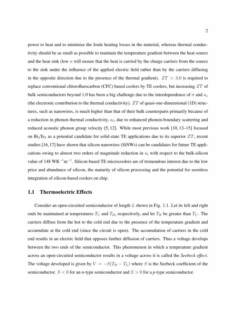
Consider an open-circuited semiconductor of length L shown in Fig. 1.1. Let its left and right
ends be maintained at temperatures TC and TH , respectively, and let TH be greater than TC . The
carriers diffuse from the hot to the cold end due to the presence of the temperature gradient and
accumulate at the cold end (since the circuit is open). The accumulation of carriers in the cold
end results in an electric field that opposes further diffusion of carriers. Thus a voltage develops
between the two ends of the semiconductor. This phenomenon in which a temperature gradient
across an open-circuited semiconductor results in a voltage across it is called the Seebeck effect.
The voltage developed is given by V = −S(TH − TL) where S is the Seebeck coefficient of the
semiconductor. S < 0 for an n-type semiconductor and S > 0 for a p-type semiconductor.
3
+ V
TH TC
Figure 1.1 Schematic to illustrate the Seebeck effect. A temperature gradient across the length of
an open-circuited semiconductor results in a voltage V across it.
The phenomenon by which a thermal gradient is induced between two junctions of dissimilar
conductors (contact #1 and #2 in Fig. 1.2) because of the flow of an electrical current is called
the Peltier effect and is characterized by Π, the Peltier coefficient of the material. The Peltier effect
arises because the carriers carry different amounts of heat in different materials, but the circuit
constraints the electric current to be constant. The two thermoelectric effects are related by the
Kelvin relation Π = ST . Fig. 1.2 shows a semiconductor with two metal contacts maintained at a
constant temperature T . Let J be the current per unit area flowing through it. The heat flux due to
this current is given by JQM = ΠMJ and JQS = ΠSJ in the metal and semiconductor, respectively,
where ΠM and ΠS are the Peltier coefficients of the metal and the semiconductor. Since the current
through the structure is constant, the difference in the heat current at contact #1 and contact #2
are given by ∆JQ1 = JQin − JQout = (ΠM − ΠS)J and ∆JQ2 = JQin − JQout = (ΠS − ΠM)J,
respectively. If ΠS is more negative than ΠM , ∆JQ1 > 0 at contact #1, whereas ∆JQ2 < 0 at
contact #2, i.e., heat is released at contact #1 and heat is absorbed at contact #2. Thus, contact
#1 will get hot while the other contact will get cold.
These two thermoelectric effects are reversible. The two irreversible effects that lower the effi-
ciency of the thermoelectric devices below the thermodynamic limit are Joule heating and thermal
conduction. The former results in a loss of heat due to the resistivity of the material, whereas the

4
∆JQ2 ∆JQ1
I
Contact
#2
Contact
#1
n-type semiconductor I
Figure 1.2 Schematic to illustrate the Peltier effect. A current through the semiconductor results
in removal of heat at contact #1 and heating at contact #2 due to the difference in the heat
carried by the carriers in different materials.
latter results in the flow of heat that opposes the temperature gradient which has to be maintained
for the proper operation of a TE device. These two effects should be minimized in thermoelectric
devices.
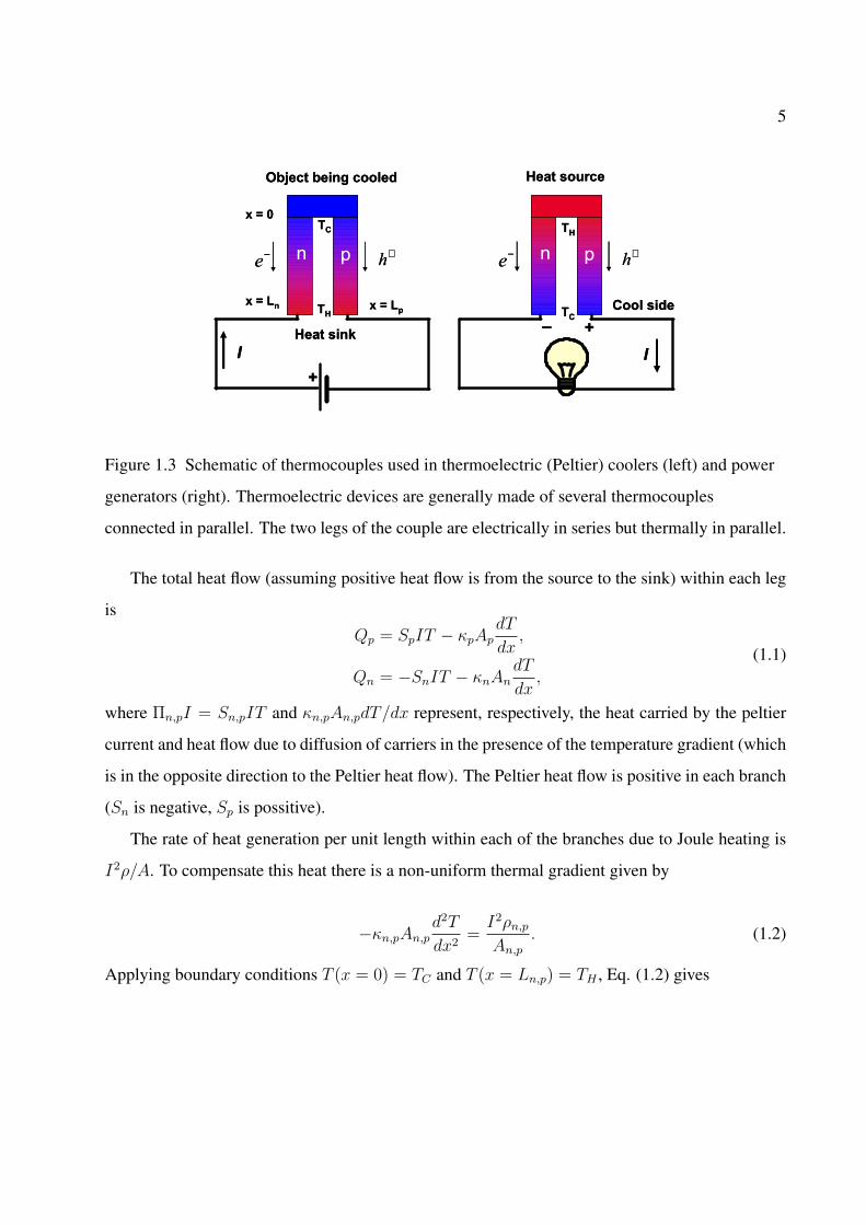
1.2 Figure Of Merit For Thermoelectric Cooling
To calculate the the figure of merit of a thermoelectric cooler, let us consider the schematic
shown in the left panel of Fig. 1.3 (the right panel shows the schematic of a thermoelectric genera-
tor - the same figure of merit can be shown to describe the efficiency of a thermoelectric generator
also) [18, 19]. When a current flows, both electrons and holes move from the top to the bottom,
thereby cooling the top due to the Peltier effect. Let A, L, S, Π, κ, and ρ be the cross sectional
area, length, Seebeck coefficient, Peltier coefficient, thermal conductivity, and electrical resistiv-
ity of each leg of the thermocouple. Subscripts n and p indicate the quantity corresponding to
the n and p branch, respectively. Let us assume that the only electrical resistance is that of the
thermocouple branches and that the only paths for heat flow between the source and the sink are
thermocouple branches, i.e., we assume there is no transfer of heat through the ambient, convec-
tion, and radiation.
5
−e
n p +h
+
Heat sink
I
Object being cooled
TC
TH
x = 0
x = Ln x = Lp
−e
n p +h
+
Heat sink
I
Object being cooled
TC
TH
x = 0
x = Ln x = Lp
Heat source
−e
n p +h
+–
Cool side
I
TH
TC
Heat source
−e
n p +h
+–
Cool side
I
TH
TC
Figure 1.3 Schematic of thermocouples used in thermoelectric (Peltier) coolers (left) and power
generators (right). Thermoelectric devices are generally made of several thermocouples
connected in parallel. The two legs of the couple are electrically in series but thermally in parallel.
The total heat flow (assuming positive heat flow is from the source to the sink) within each leg
isQp = SpIT − κpAp
dT
dx,
Qn = −SnIT − κnAndT
dx,
(1.1)
where Πn,pI = Sn,pIT and κn,pAn,pdT/dx represent, respectively, the heat carried by the peltier
current and heat flow due to diffusion of carriers in the presence of the temperature gradient (which
is in the opposite direction to the Peltier heat flow). The Peltier heat flow is positive in each branch
(Sn is negative, Sp is possitive).
The rate of heat generation per unit length within each of the branches due to Joule heating is
I2ρ/A. To compensate this heat there is a non-uniform thermal gradient given by
−κn,pAn,pd2T
dx2=
I2ρn,p
An,p
. (1.2)
Applying boundary conditions T (x = 0) = TC and T (x = Ln,p) = TH , Eq. (1.2) gives
6
−κn,pAn,pdT
dx= −
I2ρn,p
(x− Ln,p
2
)
An,p
+κn,pAn,p∆T
Lp,n
. (1.3)
Using Eq.(1.3) in Eq.(1.1), the rate at which the source is cooled (QC = (Qp + Qn)|x=0) can be
written as
QC = (Sp − Sn) ITC −K∆T − 1
2I2R, (1.4)
where K and R are the total thermal conductance (in parallel) and the resistance (in series) of the
n and the p branches. They are defined by
K =κpAp
Lp
+κpAn
Ln
, R =ρpLp
Ap
+ρpLn
An
. (1.5)
Thus the total extra load on the thermoelectric current (power in) is the sum of the diffusive heat
flow due to the total thermal conductance of the two branches and exactly half of the energy lost
due to the total Joule heating in the two branches (note that one half of the heat due to the Joule
heating goes to the source and the other half ends up in the sink).
The electrical power consumed (W ) by the thermocouple is the sum of the power lost due to
Joule heating and the work done against the Seebeck voltage:
W = I (Sp − Sn) ∆T + I2R. (1.6)
The coefficient of performance (φ) of a thermoelectric cooler is defined as the ratio of the rate at
which heat is removed from the source (QC) to the rate at which electrical energy is consumed by
the thermocouple (W ). From Eq. (1.4) and Eq. (1.6)
φ =(Sp − Sn) ITC −K∆T − 1
2I2R
I (Sp − Sn) ∆T + I2R. (1.7)
If there are no irreversible effects, we would find φ = TC/∆T , the Carnot limit for cooling. The
current corresponding to the maximum coefficient of performance φmax is obtained by settingdφdI
= 0. This gives the current
7
Iφmax =(Sp − Sn) ∆T
R (1 + ZTM)1/2 + R, (1.8)
where TM = (TC + TH) /2 is the mean temperature and Z = (Sp − Sn)2 /RK is the figure of
merit. Substituting Iφmax in Eq. (1.7), the maximum coefficient of performance can be written as
φmax =TC
[(1 + ZTM)1/2 − TH/TC
]
∆T[TC (1 + ZTM)1/2 + 1
] (1.9)
It can be seen that φmax tends to the Carnot efficiency TC/∆T when ZTM →∞. Therefore, ZTM
characterizes the efficiency of a TE material and it has to be as high as possible. To have high Z,
the Seebeck coefficients should be large and of opposite signs in the two branches, while thermal
conductance and electrical resistance should be low. The figure of merit can be seen as a parameter
which indicates that the reversible thermoelectric effects should dominate over irreversible effects,
such as heat conduction and Joule heating.
Z of a thermocouple depends on the dimensions of its branches. It can be maximized by
minimizing RK. From Eq. (1.5), we can show that product RK is minimal when
LnAp
LpAn
=
(ρpκn
ρnκp
)1/2
. (1.10)
With this condition, the figure of merit becomes
Z =(Sp − Sn)2
[(κpρp)
1/2 + (κpρp)1/2
]2 . (1.11)
Maximizing Z becomes complicated because it involves optimizing the material properties of both
legs of the thermocouple. Therefore, figure of merit is generally defined for a given single material
as
Zp,n =S2
p,nσp,n
κp,n
, (1.12)
where σp,n = 1/ρp,n. This figure of merit is equal to the actual figure of merit only in few spe-
cial cases. One such case is when the n and p branches have equivalent material properties i.e.,
8
Sp = −Sn and σp/κp = σn/κn. Another case is when one of the legs is a superconductor (for a
superconductor, the Seebeck coefficient and resistivity are zero).
σ
κ S
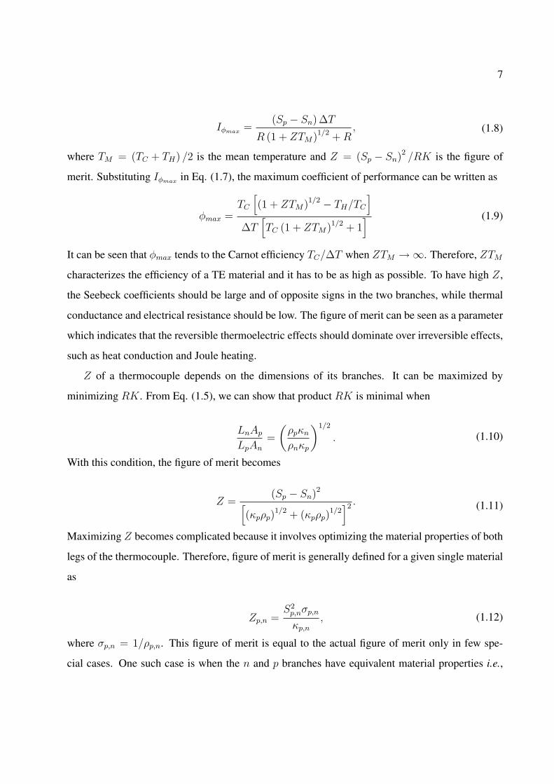
Figure 1.4 Variation of electrical and thermal conductivity, the Seebeck coefficient, and the
thermoelectric figure of merit in insulators, semiconductors, and metals. ZT is found to be
maximum in semiconductors.
1.3 Semiconductors in Thermoelectric Applications
The problem in maximizing ZT lies within the fact that S, σ, and κ are interdependent. In-
creasing σ is generally accompanied by an increase in κ and a decrease in S. Fig. 1.4 shows
the general variation of the three coefficients that determine ZT in insulators, semiconductors,
and metals. Though insulators have a high S, they are extremely resistive to the current flow,
and therefore poor candidates for TE applications. Metals, on the other hand, have a very high
σ because they have a high electron density. Metals also have equally high κ because the major-
ity heat carriers in metals are electrons. σ and κ in metals are related by the Wiedemann-Franz
law, κ ∼= κe = π2/3(KB/e)2Tσ, where KB is the Boltzmann constant and T is the temperature.
9
Therefore, increasing σ results in increased κe. This rules out the possibility of using metals for
TE applications.
In the case of semiconductors, thermal and electrical conductivity are almost decoupled. The
former is dominated by phonons whereas the latter is completely determined by either electrons or
holes (depending on semiconductor type). This fact can be used to simultaneously increase σ and
decrease κ, which makes semiconductors ideal for TE applications.
Some of the desired properties of the semiconductors that are used for TE applications are
listed below:
• Highly symmetric crystal structure, so that there are multiple band extrema which in turn
results in high DOS near the Fermi Level. This will result in high S. Narrow bandgap of the
order of 10 KBT has also been shown to result in high S.
• Non-polar, so that the polar optical phonon scattering is not present. This will decrease the
electron scattering rate and therefore result in high σ.
• Crystals with heavy atoms, so that acoustic phonons have a small group velocity. This will
decrease κ.
• Large unit cell with many atoms per unit cell, so that there are many optical phonon modes.
Optical modes have much lower velocity than the acoustic modes. If there are more optical
modes, then most of the heat will be carried by the optical modes that have very low velocity.
This will result in low κ.
• Alloys of different materials, so that the mass-difference scattering of phonons results in low
κ.
1.4 Motivation for this Work
Fig. 1.5 shows the progress made in obtaining a higher TE figure of merit over the past 60
years. Goldsmid and Douglas [13] in 1954 used Bi2Te3 for their initial study of TE refrigeration
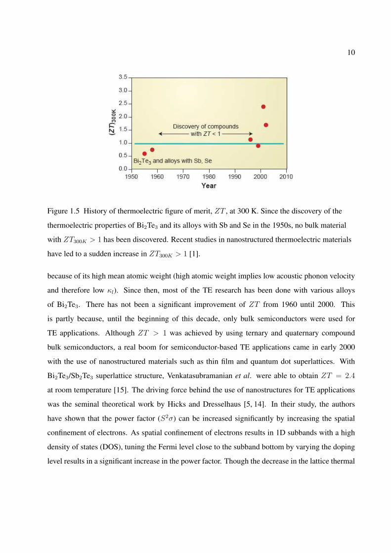
10
Figure 1.5 History of thermoelectric figure of merit, ZT , at 300 K. Since the discovery of the
thermoelectric properties of Bi2Te3 and its alloys with Sb and Se in the 1950s, no bulk material
with ZT300K > 1 has been discovered. Recent studies in nanostructured thermoelectric materials
have led to a sudden increase in ZT300K > 1 [1].
because of its high mean atomic weight (high atomic weight implies low acoustic phonon velocity
and therefore low κl). Since then, most of the TE research has been done with various alloys
of Bi2Te3. There has not been a significant improvement of ZT from 1960 until 2000. This
is partly because, until the beginning of this decade, only bulk semiconductors were used for
TE applications. Although ZT > 1 was achieved by using ternary and quaternary compound
bulk semiconductors, a real boom for semiconductor-based TE applications came in early 2000
with the use of nanostructured materials such as thin film and quantum dot superlattices. With
Bi2Te3/Sb2Te3 superlattice structure, Venkatasubramanian et al. were able to obtain ZT = 2.4
at room temperature [15]. The driving force behind the use of nanostructures for TE applications
was the seminal theoretical work by Hicks and Dresselhaus [5, 14]. In their study, the authors
have shown that the power factor (S2σ) can be increased significantly by increasing the spatial
confinement of electrons. As spatial confinement of electrons results in 1D subbands with a high
density of states (DOS), tuning the Fermi level close to the subband bottom by varying the doping
level results in a significant increase in the power factor. Though the decrease in the lattice thermal
11
conductivity with increasing spatial confinement was not considered, Hicks and Dresselhaus have
shown that ZT > 10 is possible in nanowires with extremely small cross sections (< 1 × 1 nm2).
Since then, our understanding of transport of both charge and heat in nanostructures has changed
substantially, but is far from mature [16,20]. It is now known [12,16,17,20–23] that heat transport
becomes substantially different on the nanoscale, and researchers have started to appreciate the
role of acoustic phonon confinement [12, 21, 23–25] and the influence of the boundaries on both
charge and heat transport [16, 20, 25, 26].
Silicon has been largely ignored by the TE researchers because ZT = 0.01 for bulk silicon,
almost two orders of magnitude smaller than that of materials such as Bi2Te3 and well below the
ZT of thin-film superlattice structures [15]. The primary reason for such a low ZT in bulk silicon
is that it has a high thermal conductivity. But, early this year there were two back-to-back papers
in Nature showing ZT close to 1 in SiNWs [16, 17], which is nearly a 100-fold increase with
respect to the ZT of bulk silicon. Boukai et al. [17] attribute this increase to the phonon-drag (Sph)
contribution to the thermopower S. The other paper [16], focusing on rough silicon nanowires,
attributed the increase in ZT to the decrease in κl by two orders of magnitude as a result of phonon
scattering from the boundary, roughness features and point defects. However, the decrease is κl,
especially in thinner wires, could not be explained by accepted theory [12, 24], and the authors
speculate [16] that a phenomenon such as phonon localization may be taking place.
Though recent reports of high ZT in SiNWs is good news for the semiconductor industry (be-
cause of the various advantages of silicon listed before), the lack of theoretical understanding of
the observed increase in ZT in them is a serious concern because it prevents us from optimiz-
ing the wires for TE applications. Optimization of SiNW ZT requires a detailed knowledge of
their electronic and thermal properties. Unfortunately, so far, we have insufficient theoretical and
experimental data on both.
The effect of increasing spatial confinement on the variation of κl in nanowires has been ex-
tensively studied over the past few years [12, 21, 24, 27, 28], but there are still uncertainties. A
reliable estimate of ZT for a nanowires also requires a thorough understanding of the size effects
on the electronic portion of thermal conductivity (κe), the Seebeck coefficient (S), and electrical

12
conductivity (σ). Room-temperature electron transport in relatively long nanowires received less
attention than heat transport, and until recently there was little consensus as to how these structures
actually behave. Recent studies of the electron mobility in SiNWs show a non-trivial variation of
the electron relaxation times with decreasing SiNW dimensions [25, 26]. As electron relaxation
determines the variation of S, κe, and σ, calculation of these parameters by solving the electron
Boltzmann transport equation (BTE) becomes very important.
1.5 Aims of this Work
The primary objective of this work is to develop a thermoelectric simulator to compute ZT of
SiNWs. This involves three parts: 1). Developing an electronic simulator to study the diffusive
(dominated by scattering) electron transport in SiNWs; 2). Developing a phononic simulator to
study the diffusive phonon transport in SiNWs; 3). Couple the two simulators to calculate ZT of
SiNWs.
1.5.1 Electron Transport Simulator
• Develop a self-consistent Poisson-Schrodinger solver to obtain the potential profile and the
electronic wavefunctions in SiNWs.
• Derive the scattering rate of electrons due to acoustic phonons (both bulk and confined),
intervalley phonons, roughness at Si/SiO2 interface, and impurities. This should account for
the one-dimensional (1D) nature of electrons and include scattering to various valleys and
subbands.
• Calculate the acoustic phonon dispersion in nanowires. As acoustic phonons are also con-
fined in SiNWs, the modified dispersion in them needs to be calculated.
• Develop a 1D Monte-Carlo simulator to solve the electron Boltzmann transport equation
(BTE). Calculate the electron mobility and electrical conductivity in gated and ungated
SiNWs.
13
• Derive the expression for the electronic contribution to thermal conductivity and the Seebeck
coefficient from the 1D electron BTE and compute them.
The results from this part of the work have led to four conference presentations [29–32] and four
journal publications [25, 33–35]. A comprehensive study of electronic transport in SiNWs is pre-
sented in Chapter 2.
1.5.2 Phonon Transport Simulator
• Develop a Monte Carlo transport kernel to compute κl in SiNWs using bulk phonons.
• Use the full acoustic phonon dispersion calculated previously in the Klemens-Callaway ex-
pression to compute κl in SiNWs.
• Derive the lattice thermal conductivity from the 1D phonon BTE accounting for 2D confine-
ment of acoustic phonons.
• Derive the expression for the scattering rate of phonons with other phonons, electrons, im-
purities, and rough boundaries, by properly accounting for 2D confinement of phonons and
electrons in NWs. Compute the κl from the expression derived from 1D phonon BTE.
• Develop a Monte Carlo phonon transport kernel to calculate the κl in SiNWs. This should
use the full dispersion of SiNWs and the 1D phonon scattering rates calculated previously.
• Generate the surface of SiNWs from a given exponentially varying autocorrelation function
and use it in the Monte Carlo transport kernel to capture the effect of phonon localization at
the boundaries of the wire.
The results from this part of the work have led to two conference presentations [36, 37] and one
journal publication [28].
1.5.3 Thermoelectric Simulator
• Use σ, S, and κl (obtained using the Klemens-Callaway expression) to get an estimate of the
ZT of SiNWs.

14
• Use σ, S, and κl (obtained with confined acoustic phonons and a Monte Carlo transport
kernel) to accurately compute the ZT of SiNWs.
The results from this part of the work have led to eight conference presentations [38–45] (nom-
inated for best paper award) and one journal paper in preparation [46]. The study of thermal
transport and the ZT computed from the electrothermal (coupled electron and thermal) simulator
are presented in Chapter 3.
The summary and direction for the future extension of this work are presented in Chapter
4. The expressions for the electron scattering rates (with acoustic phonons, intervalley phonons,
impurities, and interface roughness) that are used in the electron Monte Carlo transport kernel,
are derived in Appendix A. The details of the self-consistent Poisson-Schrodinger-Monte Carlo
solver which was developed to simulate the electron transport in SiNWs is presented in Appendix
B. Finally, the details of the Monte Carlo kernel which solves the phonon BTE is presented in
Appendix C.
15
Chapter 2
Electronic Transport in Silicon Nanowires
2.1 Historical Overview
The study of electronic transport in nanowires started almost three decades ago with the semi-
nal work by Sakaki [47] in 1980. Sakaki showed that the elastic scattering in nanowires (NWs) is
suppressed drastically due to a reduction in the final density of states (DOS) for scattering. Elec-
trons in NWs are confined in two transverse directions and are free to move only along the axis of
the wire. In the extreme quantum limit (electrons occupy only the lowest subband), for an elastic
scattering process, an electron in the initial state ki can only be scattered to the final state kf = −ki
accompanied by a large change in momentum (2ki), since the 1D constant energy surface has only
two discrete states. In the case of bulk structures, the constant energy surface is a sphere of radius
ki, so electrons can be scattered to various states including those in the vicinity of ki. Sakaki con-
sidered scattering from remote impurities and showed that the mobility as high as 108 cm2/Vs can
be achieved in GaAs NWs at low temperatures because of the substantial reduction of the DOS for
scattering in NWs. While the approximations in this work would underestimate the effect of impu-
rities located close to the wire and remote impurity scattering is certainly not the only mechanism
limiting the mobility in NWs, the work of Sakaki provided strong impetus for the further study of
electronic transport in quasi-1D structures.
In the following year, Arora [48] calculated the scattering rate due to acoustic phonons and
point defects in thin rectangular wire under the relaxation time approximation (RTA) and found
them both to increase with decreasing wire cross section. He also showed that the ratio of the
conductivity in the wire to the bulk conductivity is proportional to the area of the wire cross
16
section. This result contradicts the previous result of Sakaki, who assumed Coulomb scattering
from remote impurities alone in the calculation of the mobility. Lee and Spector [49] calculated
the impurity-limited mobility by accounting for both background and remote impurities using the
same approximation as in Sakaki’s work. They found the scattering rate from background impu-
rities to be much higher than that from the remote impurities and independent of the wire cross
section (probably lost due to the delta-function approximation of wavefunctions along the trans-
verse directions). They also confirmed the acoustic phonon-limited mobility trend in NWs shown
by Arora.
Lee and Vassel [50] considered scattering of electrons from acoustic phonons, impurities (both
remote and background), and polar optical phonons and calculated the mobility in wires of various
cross sections and different temperatures. For the whole temperature range, they found the mobility
in NWs to decrease with decreasing wire cross section. At very low temperatures, where the
scattering from impurities dominates transport, mobility in NWs was found to be higher than that
in bulk. At room temperature, where phonons dominate electron transport, the mobility in wires of
cross section smaller than 12 x 12 nm2 was found to be lower than that of the bulk, but for larger
cross sections the mobility of the wire was greater than in the bulk.
2.1.1 Electronic Bandstructure Modification in Nanowires
All the work discussed above was done on GaAs NWs, with the bulk bandstructure, and assum-
ing unconfined phonons as in the bulk. Sanders et al. [51], in their work on the electronic transport
in free-standing silicon nanowires (SiNWs), indicated yet another important consequence of 2D
confinement of electrons in NWs – the modification of the electronic bandstructure because of the
change in the dimensionality of the Brillouin zone. The Brillouin zone becomes 1D in NWs since
the crystal structure is periodic only along the wire axis. Sanders et al. considered SiNWs with
axis along [001] and the faces of the wire are 110. The primitive cell from which the wire is
constructed is shown in Fig. 2.1. It contains four silicon atoms (as opposed to only two atoms in
a bulk silicon primitive cell); the length of the primitive cell along the axis is a and the transverse
dimensions are a/√
2, where a is the lattice constant (a = 5.43A). The Brillouin zone in SiNWs

17
Figure 2.1 Crystal structure of an idealized silicon NW. The NW unit cell is shown on the right.
Each base unit contains four atoms. The faces are parallel to the four equivalent 110 planes and
the wire is oriented along [001].
is 1D and it extends from −π/a to +π/a, as opposed to −2π/a to +2π/a in bulk silicon along
[100]. This is because of the doubling of the length of the unit cell along the wire axis. The
conduction band in bulk silicon is indirect and is composed of six equivalent ∆ valleys located at
±0.85× (2π/a) = ±1.7π/a along each of the <100> directions. In case of the SiNWs with axis
along [001], four of the ∆4 valleys along the transverse directions ([010], [010], [100], and [100])
are projected onto the Γ point in the 1D Brillouin zone and their energies are determined by the
effective masses along the [110] and [110] confinement directions. The two ∆2 valleys along [001]
of the bulk Brillouin zone are zone-folded to ±0.3π/a in SiNWs and become the off-Γ states. The
energy bands derived from these are at higher energies than those at the Γ point since the [001]
18
Figure 2.2 Bandstructures of square SiNWs of three different widths. The Brillouin zone is 1D
with k ranging from −π/a to +π/a.
valleys have a lighter effective mass in both confining directions. Thus the SiNW becomes a direct
bandgap material.
The work of Sanders et al. paved the way for the study of the effects of electronic bandstructure
modification on the ballistic transport in silicon nanowire transistors (SWNT) by various groups
[52–58]. Using the bandstructure obtained from a tight-binding model, Wang et al. [52] studied
the validity of using the bulk effective mass in the calculation of electrical properties in SNWTs
of different side lengths a. The bulk effective mass was found to overestimate both the threshold
voltage (for a < 3 nm) and the ON-current (for a < 5 nm). Zheng et al. [53] calculated the
effective masses, valley splitting between the ∆4 (at Γ point) and the ∆2 (off- Γ point) bands,
and the bandgap from the full SiNW bandstructure obtained using the tight-binding model. All
three were found to increase with decreasing wire cross section. They also found that the single
band effective mass equation predicts the bottom of energy bands accurately. Bandstructure in
SiNWs is also found to depend on the orientation of the wire axis [54] and the species used for
surface termination [56]. For all orientations and surface terminations studied, SiNWs were found
to exhibit direct bandgap.
19
Figure 2.3 (Left panel) The dispersion of the dilatational modes in a 28.3 × 56.6 A GaAs. The
dashed lines are the dispersion curves of bulk LA and TA waves along the [001] direction. (Right
panel) Confined acoustic phonon-electron scattering rate as a function of electron energy. The
dashed and the solid lines indicate the deformation potential (DP) scattering rate and scattering
rate due to both DP and ripple mechanism (RP) combined, respectively [2].
2.1.2 Acoustic Phonon Confinement in Nanowires
Another important consequence of 2D spatial confinement in NWs is the modification of the
acoustic phonon dispersion in them. In ultrasmall structures such as NWs, the acoustic phonon
spectrum is modified due to the mismatch of the sound velocities and mass densities between
the active layer and the surrounding material [59]. The modified dispersion is obtained by the
solving elastic continuum equation subject to proper boundary conditions at the surface of the
wire: the normal component of the stress tensor vanishes for a free-standing wire and displacement
becomes zero for a rigidly clamped wire. For free-standing wires, the overall group velocity of
acoustic phonons decreases with increasing spatial confinement and this results in higher electron-
phonon scattering rates [2, 60–62]. Although Yu et al. [60] were the first to show the increase in
electron-acoustic phonon scattering in rectangular NWs, they assumed that the width of the wire
is much larger than the thickness of the wire and used Morse formalism [63] in the calculation of
acoustic phonon dispersion. Nishiguchi [3] was the first to derive the exact dispersion of acoustic
20
phonons in free-standing NWs of rectangular cross section. In his work he also showed that the
Morse formalism captures only the first phononic mode correctly. The dispersion [3] and the
scattering rates [2] calculated by Nishiguchi are shown in Fig. 2.3. Only intrasubband scattering
was accounted for in his study.
Experimental results on electronic transport in SiNWs were first reported by Cui et al. in 2003.
The mobility in SiNWs was found to be higher than in bulk silicon. The increase in mobility
was attributed to the reduced DOS for scattering as suggested by Sakaki [47]. In the following
year, Koo et al. [64] also reported the electron mobility in SiNW FETs to be two times higher
than that in bulk MOSFETs, supporting the results of Cui et al. In the same year, Kotlyar et
al. [65] showed that the phonon-limited mobility in SiNWs is much lower than that in the bulk
silicon because of the increase in the electron-phonon wavefunction overlap with decreasing cross
section. Unlike all previous theoretical studies of transport in NWs, they considered a detailed
multisubband transport and used the electronic wavefunctions and subbands obtained from solving
coupled Schrodinger and Poisson equations self-consistently in the calculation of the scattering
rates. Wang et al. reported that the surface roughness scattering (SRS) becomes less important
in the case of ultrasmall SiNWs [66]. Jin et al. [26] did a detailed calculation of both phonon-
limited and SRS-limited mobility in cylindrical SiNWs and found both to decrease with decreasing
wire cross section. A similar mobility reduction in SiNWs has been reported this year by both
theoretical [25, 67] and experimental groups [68].
2.2 Preliminary Research : Electron Mobility in SiNWs
The results on the study of diffusive electron transport in SiNWs presented in this section were
taken from two of my journal papers:
1. E.B. Ramayya, D. Vasileska, S.M. Goodnick, and I. Knezevic, ”Electron mobility in silicon
nanowires,” IEEE Transactions on Nanotechnology 6, 113-117 (2007).
21
2. E.B. Ramayya, D. Vasileska, S.M. Goodnick, and I. Knezevic, ”Electron transport in sili-
con nanowires: the role of acoustic phonon confinement and surface roughness scattering,”
Journal of Applied Physics 104, 063711 (2008).
2.2.1 Introduction and Motivation
The low-field electron mobility is one of the important parameters that determines the per-
formance of field-effect transistors (FETs), thermoelectric (TE) coolers and sensors. Although
its importance in ultra-short channel MOSFETs has been debated [69, 70], it certainly affects the
conductivity of the wire interconnects, the figure of merit of TE coolers and the responsiveness
of nanowire sensors. The study of the electron mobility in SiNWs so far has been inconclusive:
Kotlyar et al. [65], Jin et al. [26], and more recently other research groups [25, 67, 68, 71] have
shown that the mobility in a SiNW decreases with cross section, whereas the works of Sakaki [47],
Cui et al. [72], Koo et al. [64], and Sharma et al. [73] show higher mobility in SiNWs compared
to bulk MOSFETs. The contradiction stems from two opposing effects that determine the electron
mobility as we move from 2D to 1D structures: one is a decrease in the density of states (DOS) for
scattering [47] that results in reduced scattering rates and thereby an enhancement in the mobility;
the second is an increase in the so-called electron-phonon wavefunction overlap [65] that results
in increased electron-phonon scattering rates and consequently lower mobility. While important,
these two competing phenomena do not paint a full picture of low-field transport in SiNWs, in
which the effect of spatial confinement on the scattering due to surface roughness and acoustic
phonons must be addressed.
Surface roughness scattering (SRS) is by far the most important cause of mobility degradation
in conventional MOSFETs at high transverse fields. Intuitively, one would expect the SRS to be
even more detrimental in SiNWs than conventional MOSFETs because SiNWs have four Si-SiO2
interfaces, as opposed to one such interface in conventional MOSFETs. Although recent work has
shown that the SRS is in fact less important in SiNWs than in bulk MOSFETs due to a reduction in
the DOS [66] and the onset of volume inversion (redistribution of electrons throughout the silicon
22
channel) [33], a detailed study of the SRS-limited mobility in cylindrical SiNWs by Jin et al. [26]
shows a rapid monotonic decrease of mobility for wire diameters smaller than 5 nm.
Scattering due to acoustic phonons is significantly altered in nanostructures due to the mod-
ification of the acoustic phonon spectrum in them. Extensive work on the effects of acoustic
phonon confinement in III-V based nanostructures [74, 75] shows a lower acoustic phonon group
velocity [76,77], lower thermal conductivity [12,78,79], and increased acoustic phonon scattering
rates [60, 62] in nanoscale devices compared to their bulk counterparts. As for silicon nanostruc-
tures, there is experimental evidence of the acoustic phonons confinement in nanomembranes [80],
while recent work on SOI MOSFETs [81–83] and ultra-small SiNWs [58] also show that the bulk
phonon (linear dispersion) approximation overestimates the mobility.
In this chapter, we compute the electron mobility in gated SiNWs with rectangular and square
cross section by accounting for the scattering of electrons due to confined acoustic phonons, inter-
valley phonons, and imperfections at the Si-SiO2 interface. Bulk silicon effective mass parameters
are used in the calculation of the scattering rates. The confined acoustic phonon spectrum is ob-
tained by using the xyz algorithm [3,84] and the unscreened SRS is modeled using modified Ando’s
model [85] that accounts for the finite thickness of the silicon layer. Our detailed analysis clearly
shows that the mobility in SiNWs calculated by accounting for acoustic phonon confinement is
about 10% lower than that calculated by treating acoustic phonons under bulk approximation. Also,
the expected enhancement of mobility due to subband modulation (redistribution of electrons in
energy space) [86–88] and volume inversion (redistribution of electrons in real space) [33, 89] are
offset by the increase in the confinement induced component of the SRS and consequently, the
mobility decreases with decreasing wire cross section.
The electronic bandstructure in SiNWs has been shown to be significantly altered from that of
the bulk silicon due to the Brillouin zone folding [51–53,58]. The bandstructure modification will
certainly affect the intervalley scattering rates in SiNWs, but deformation potentials and phonon
energies needed to describe the intervalley scattering are still only available for bulk silicon. There-
fore, in order to be consistent, we do not employ the exact nanowire bandstructure, but rather rely
on the bulk Si bandstucture and then solve the two-dimensional Schrodinger equation within the
23
the envelope function and effective mass framework in order to calculate the SiNW electron sub-
bands. The splitting of the six fold degenerate ∆ valleys of silicon due to the mass difference
in different confining directions is automatically accounted for by including the anisotropy of the
effective mass of electrons (see Sec. 2.2.6.1).
Thin SOI layer
(8 nm)
Gate
Buried Oxide
(80 nm)
n+
Gate Oxide
(25 nm)
Si Substrate
(700 nm)
x
y
z
n+
p-
Thin SOI layer
(8 nm)
Gate
Buried Oxide
(80 nm)
n+
Gate Oxide
(25 nm)
Si Substrate
(700 nm)
x
y
z
n+
p-
Figure 2.4 Schematic of the simulated 8×8 nm2 SiNW on ultrathin SOI.
2.2.2 Device Structure and Simulator Components
A schematic of the device considered in our study is shown in the Fig. 2.4. It is a modified
version of the ultra-thin, ultra-narrow SOI MOSFET that was originally proposed by Majima et
al. [90]. The thickness of the gate oxide, buried oxide, and bottom silicon substrate are 25 nm,
80 nm, and 700 nm, respectively. The width of the channel is varied from 30 nm to 8 nm and the
thickness of the channel is fixed at 8 nm Section 2.2.4 and in the rest of the study the transverse
dimensions of the silicon channel are varied from 8 × 8 nm2 to 3 ×3 nm2. For all the gated
wire cross sections considered, the width of the oxide on both sides of the channel is 200 nm, the
24
channel is doped to 3 × 1015 cm−3, and the channel is assumed to be homogeneous and infinitely
long.
Poisson Solver
Schrödinger Solver
Monte Carlo
Transport Kernel
Low Field Electron Mobility
Surface Roughness
Acoustic Phonons
Intervalley Phonons
SOR
ARPACK
Poisson Solver
Schrödinger Solver
Monte Carlo
Transport Kernel
Low Field Electron Mobility
Surface Roughness
Acoustic Phonons
Intervalley Phonons
SOR
ARPACK
Figure 2.5 Flowchart of the simulator developed to calculate the electron mobility in SiNWs.
The simulator developed to calculate the electron mobility has two components: the first is
a self-consistent 2D Poisson-2D Schrodinger solver and the second is a Monte-Carlo transport
kernel. The former is used to calculate the electronic states and the self-consistent potential distri-
bution along the cross section of the wire and the latter simulates the transport along the wire axis.
The finite barrier at the Si-SiO2 interface results in the electron wavefunction penetration through
the interface and into the oxide. The wavefunction penetration is accounted for by including a
few mesh points in the oxide while solving the Schrodinger equation. ARPACK package [91] was
used to solve the 2D Schrodinger equation and successive over-relaxation (SOR) method was used
to solve the 2D Poisson equation. The convergence of the coupled Schrodinger-Poisson solver is
found to be faster when Poisson equation is solved using SOR method than when Poisson equation
is solved using incomplete LU (ILU) method.
The Monte Carlo transport kernel is used to simulate the electron transport along the axis of
the wire under the influence of the confining potential in the transverse directions and a very small
lateral electric field along the channel. The long wire approximation implies that the transport
is diffusive (the length exceeds the carrier mean free path), and therefore justifies the use of the
Monte Carlo method [92,93] to simulate electron transport. Electrons are initialized such that their
25
average kinetic energy is (1/2)KBT (thermal energy for 1D) and are distributed among different
subbands obtained from the Poisson-Schrodinger solver in accordance with the equilibrium dis-
tribution. Since the electrons are confined in two transverse directions, they are only scattered in
either the forward or the backward direction; consequently, just the carrier momentum along the
length of the wire needs to be updated after each scattering event. Mobility is calculated from the
ensemble average of the electron velocities [92].
2.2.3 Scattering due to Bulk Acoustic Phonons, Intervalley Phonons, and Sur-face Roughness
The SRS is modeled using Ando’s model [85], intervalley scattering was calculated using bulk
phonon approximation, and the intravalley acoustic phonons were treated in both the bulk-mode
and confined-mode approximations. Since the wire is very lightly doped, the effect of impurity
scattering was not included. Nonparabolic band model for silicon, with the nonparabolicity factor
α = 0.5eV −1, was used in the calculation of scattering rates. A detailed derivation of the 1D
scattering rates is given in Appendices A.1 (phonon scattering) and A.2 (SRS). Here, for brevity,
only the final expressions for the scattering rates are given.
For an electron with an initial lateral wavevector kx and parabolic kinetic energy Ekx = h2k2x/(2m
∗)
in subband n [with subband energy En and electron wavefunction ψn(y, z)], scattered to subband
m [with subband energy Em and electron wavefunction ψm(y, z)], the final kinetic energy Ef is
given by
Ef = En − Em +
√1 + 4αEkx − 1
2α+ hω, (2.1)
where hω = 0 for elastic (bulk intravalley acoustic phonon and surface roughness) scattering,
hω = ±hω0 for the absorption/emission of an approximately dispersionless intervalley phonon
of energy hω0, while in the case of confined acoustic phonons (below) the full phonon subband
dispersion is incorporated.
The intravalley acoustic phonon scattering rate due to bulk acoustic phonons is given by
Γacnm(kx) =
Ξ2ackBT
√2m∗
h2ρυ2Dnm
(1 + 2αEf )√Ef (1 + αEf )Θ(Ef ), (2.2)
26
where Ξac is the acoustic deformation potential, ρ is the crystal density, v is the sound velocity, and
Θ is the Heaviside step-function. Dnm represents the overlap integral associated with the electron-
phonon interaction (the so-called electron-phonon wavefunction integral [65]), and is given by
Dnm =
∫∫|ψn(y, z)|2|ψm(y, z)|2 dy dz. (2.3)
The intervalley phonon scattering (mediated by short wavelength acoustic and optical phonons)
rate is given by
Γivnm(kx) =
Ξ2iv
√m∗
√2hρω0
(N0 +
1
2∓ 1
2
)Dnm
× (1 + 2αEf )√Ef (1 + αEf )Θ(Ef ),
(2.4)
where Ξiv is the intervalley deformation potential, and Dnm is defined in (2.3). The approximation
of dispersionless bulk phonons of energy hω0 was adopted to describe an average phonon with
wavevector near the edge of the Brillouin zone and N0 = [exp(hω0/kBT )− 1]−1 is their average
number at temperature T .
Assuming exponentially correlated surface roughness [94] and incorporating the electron wave-
function deformation due to the interface roughness using Ando’s model [85], the unscreened SRS
rate is given by
Γsrnm(kx,±) =
2√
m∗e2
h2
∆2Λ
2 + (q±x )2Λ2|Fnm|2
× (1 + 2αEf )√Ef (1 + αEf )Θ(Ef ),
(2.5)
where ∆ and Λ are the r.m.s. height and the correlation length of the fluctuations at the Si-SiO2
interface, respectively. q±x = kx±k′x is the difference between the initial (kx) and the final (k′x)
electron wavevectors and the top (bottom) sign is for backward (forward) scattering. The SRS
overlap integral in Eq. (2.5) due to the top interface for a silicon body thickness of ty is given by
Fnm =
∫∫dy dz
[− h2
etymy
ψm(y, z)∂2ψn(y, z)
∂y2
+ ψn(y, z)εy(y, z)
(1− y
ty
)ψm(y, z) (2.6)
+ ψn(y, z)
(Em − En
e
)(1− y
ty
)∂ψm(y, z)
∂y
].
27
The SRS overlap integral was derived assuming the interfaces to be uncorrelated. For the
bottom interface, the integration should be performed from the bottom interface to the top interface
and the integral for the side interfaces can be obtained by interchanging y and z in Eq. (2.6). The
first term in Eq. (2.6) is the confinement-induced part of the SRS and it increases with decreasing
wire cross section. This term does not depend on the position of the electrons in the channel and
hence results in high SRS even at low transverse fields from the gate. The second and third terms
in Eq. (2.6) depend on the average distance of electrons from the interface, so they contribute to
the SRS only at high transverse fields from the gate. For wires of cross section smaller than 5 ×5 nm2, major contribution to SRS comes from the confinement-induced term in Eq. (2.6), and it
increases rapidly with decreasing wire cross section.
Scattering rates given by Eqs. (2.2)–(2.5) are calculated using the wavefunctions and potential
obtained from the self-consistent Poisson-Schrodinger solver. Parameters used for calculating the
intervalley scattering were taken from Ref. TakagiJJAP98, the acoustic deformation potential was
taken from Ref. BuinNL08, and ∆ = 0.3 nm and Λ = 2.5 nm were used to characterize the SRS
due to each of the four interfaces. The SRS parameters were obtained by fitting the mobility of
an 8 × 30 nm2 SiNW in the high transverse field region (where the SRS dominates) with the
corresponding mobility observed in ultra-thin SOI of similar thickness [88].
2.2.4 Effect of Decreasing Channel Width on Mobility
The variation of the field-dependent mobility with decreasing channel width was investigated
on a series of SiNWs, while keeping the channel thickness at 8 nm. Fig. 2.6 shows the mobility
for SiNWs with the widths of 30 nm, 16 nm and 8 nm. Two important results regarding the
mobility behavior in the width range considered can be deduced from Fig. 2.6: (i) the mobility at
high transverse fields, which is dominated by the SRS, increases with decreasing wire width and
(ii) the mobility at low-to-moderate transverse fields, determined by phonon scattering, decreases
with decreasing wire width. In the calculation of SRS overlap integral, infinite wire thickness was
assumed as in the original Ando’s derivation. With ts →∞ assumption the integral becomes
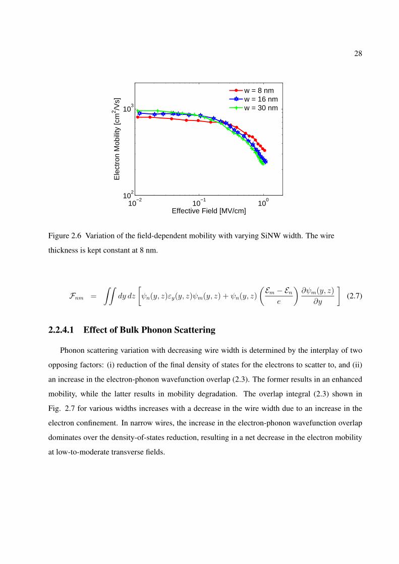
28
10−2
10−1
100
102
103
Effective Field [MV/cm]
Ele
ctro
n M
obili
ty [c
m2 /V
s]
w = 8 nmw = 16 nmw = 30 nm
Figure 2.6 Variation of the field-dependent mobility with varying SiNW width. The wire
thickness is kept constant at 8 nm.
Fnm =
∫∫dy dz
[ψn(y, z)εy(y, z)ψm(y, z) + ψn(y, z)
(Em − En
e
)∂ψm(y, z)
∂y
](2.7)
2.2.4.1 Effect of Bulk Phonon Scattering
Phonon scattering variation with decreasing wire width is determined by the interplay of two
opposing factors: (i) reduction of the final density of states for the electrons to scatter to, and (ii)
an increase in the electron-phonon wavefunction overlap (2.3). The former results in an enhanced
mobility, while the latter results in mobility degradation. The overlap integral (2.3) shown in
Fig. 2.7 for various widths increases with a decrease in the wire width due to an increase in the
electron confinement. In narrow wires, the increase in the electron-phonon wavefunction overlap
dominates over the density-of-states reduction, resulting in a net decrease in the electron mobility
at low-to-moderate transverse fields.

29
5 10 15 20 25 300
1
2
3
4
5x 10
12
Channel Width [nm]
Ove
rlap
Inte
gral
[cm
−2 ]
Figure 2.7 Variation of the overlap integral for the lowest subband with varying wire width,
obtained from (2.3) at a constant sheet density of Ns = 2.9× 1011cm−2.
2.2.4.2 Effect of Surface Roughness Scattering
The SRS overlap integral given by (2.7) has three terms. Two are due to deformation of the
wavefunction, and the third, dominant term depends on the strength of the field perpendicular to
the interface. Since the field normal to the side interfaces is very weak, SRS due to these interfaces
is much less efficient than scattering due to the top and bottom ones. The decrease in SRS with
decreasing wire width can be understood by following the behavior of the average distance (2.8)
of the carriers from the top interface:
〈y〉 =1
Nl
∑i,ν
N i,νl
∫∫|ψν
i (y, z)|2y dy dz , (2.8)
where Nl is the total line density and N i,νl is the line density in the ith subband of the νth valley.
In Fig. 2.8, we can see that the carriers are moving away from the top interface as the width of the
wire is decreased, and are therefore not strongly influenced by the interface. This behavior is also
observed in the case of ultrathin double-gate SOI FETs, and is due to the onset of volume inversion
[89, 95]. As the SiNW approaches the volume inversion limit, carriers cease to be confined to the
interfaces, but are distributed throughout the silicon volume. Fig. 2.9 shows the distribution of
carriers in a 30 nm wire and a 8 nm wire at the same effective field; we can clearly see that the
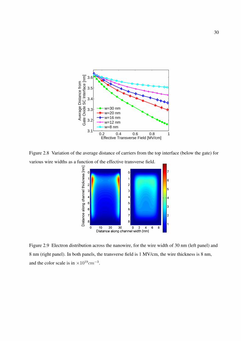
30
0.2 0.4 0.6 0.8 13.1
3.2
3.3
3.4
3.5
3.6
Effective Transverse Field [MV/cm]
Ave
rage
Dis
tanc
e fr
om
Gat
e O
xide
SC
Inte
rfac
e [n
m]
w=30 nmw=20 nmw=16 nmw=12 nmw=8 nm
Figure 2.8 Variation of the average distance of carriers from the top interface (below the gate) for
various wire widths as a function of the effective transverse field.
Figure 2.9 Electron distribution across the nanowire, for the wire width of 30 nm (left panel) and
8 nm (right panel). In both panels, the transverse field is 1 MV/cm, the wire thickness is 8 nm,
and the color scale is in ×1019cm−3.
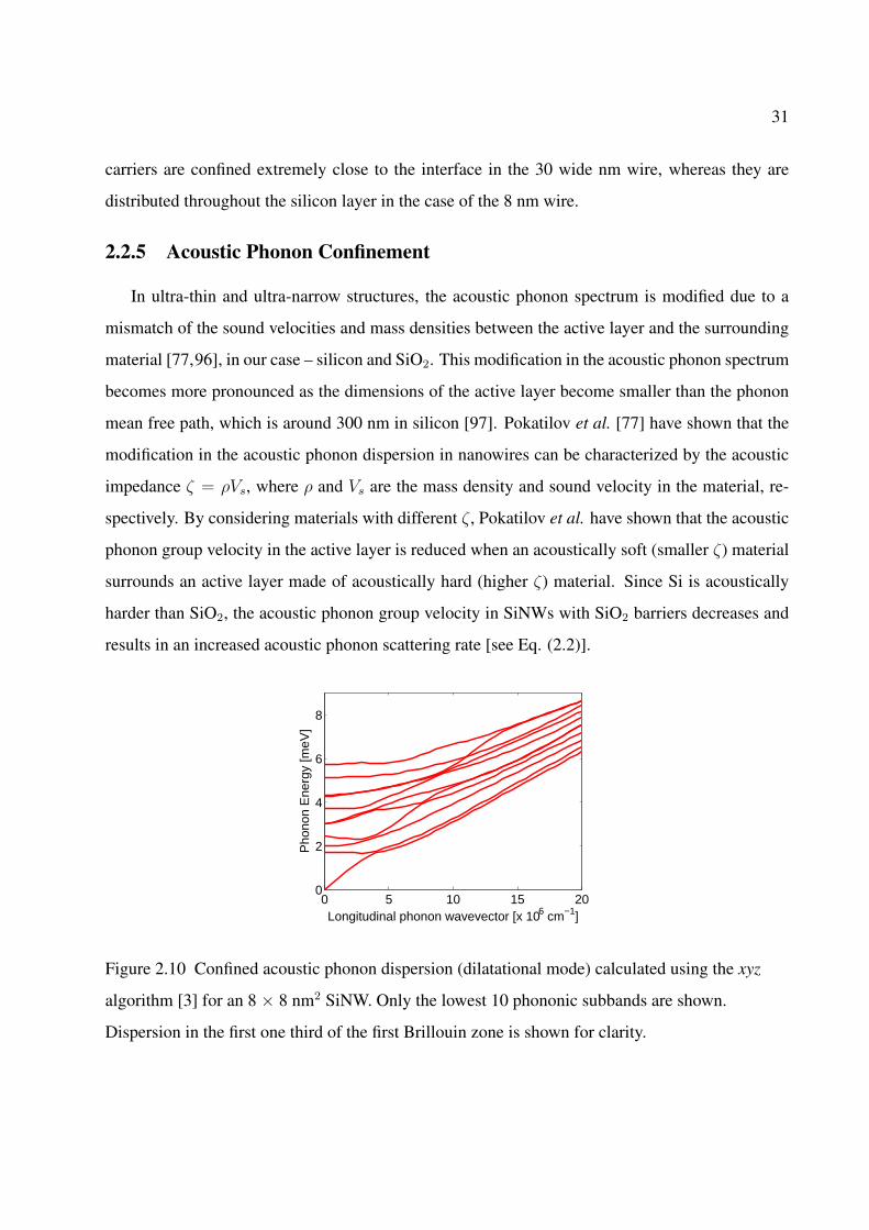
31
carriers are confined extremely close to the interface in the 30 wide nm wire, whereas they are
distributed throughout the silicon layer in the case of the 8 nm wire.
2.2.5 Acoustic Phonon Confinement
In ultra-thin and ultra-narrow structures, the acoustic phonon spectrum is modified due to a
mismatch of the sound velocities and mass densities between the active layer and the surrounding
material [77,96], in our case – silicon and SiO2. This modification in the acoustic phonon spectrum
becomes more pronounced as the dimensions of the active layer become smaller than the phonon
mean free path, which is around 300 nm in silicon [97]. Pokatilov et al. [77] have shown that the
modification in the acoustic phonon dispersion in nanowires can be characterized by the acoustic
impedance ζ = ρVs, where ρ and Vs are the mass density and sound velocity in the material, re-
spectively. By considering materials with different ζ , Pokatilov et al. have shown that the acoustic
phonon group velocity in the active layer is reduced when an acoustically soft (smaller ζ) material
surrounds an active layer made of acoustically hard (higher ζ) material. Since Si is acoustically
harder than SiO2, the acoustic phonon group velocity in SiNWs with SiO2 barriers decreases and
results in an increased acoustic phonon scattering rate [see Eq. (2.2)].
0 5 10 15 200
2
4
6
8
Longitudinal phonon wavevector [x 106 cm−1]
Pho
non
Ene
rgy
[meV
]
Figure 2.10 Confined acoustic phonon dispersion (dilatational mode) calculated using the xyz
algorithm [3] for an 8 × 8 nm2 SiNW. Only the lowest 10 phononic subbands are shown.
Dispersion in the first one third of the first Brillouin zone is shown for clarity.
32
2.2.5.1 Confined Acoustic Phonon Dispersion
The first step in accounting for the acoustic phonon confinement in mobility calculation is
to calculate the modified acoustic phonon dispersion. Using the adiabatic bond charge model [98]
(microscopic calculation, accurate but computationally involved), Hepplestone and Srivastava have
shown the validity of the elastic continuum model (macroscopic calculation, less accurate but eas-
ier to implement) for wire dimensions greater than 2.5 nm. [99] Hence, in this work we have used
the elastic continuum model to calculate the modified phonon spectrum. Most of the previous stud-
ies of acoustic phonon confinement in nanowires have used approximate hybrid modes proposed
by Morse [63] (valid for wires with thickness much less than the width) to calculate the dispersion
spectrum. Nishiguchi et al. [3] calculated the dispersion spectrum using xyz algorithm [84] and
found that the Morse formalism is valid only for the lowest phonon subband. Since one acoustic
phonon subband is surely not enough to accurately describe scattering with electrons, in this work,
we have used Nishiguchi et al.’s approach to calculate the acoustic phonon dispersion, although it
is computationally intensive. The basis functions used to expand the phonon mode displacements
in Nishiguchi et al.’s approach are powers of Cartesian coordinates, and the number of basis func-
tions required to fully describe the modes depends on the number of modes required. For an 8
× 8 nm2 SiNW, we have found that the lowest 35 phononic subbands are enough to calculate the
scattering rate. Also, we found that about 176 basis functions are sufficient to fully describe the
displacement of those 35 phononic modes. The number of phononic bands required decreases with
the decrease in wire cross section.
Two types of boundary conditions are often used to calculate the acoustic phonon spectrum in
nanostructures: a) The free-standing boundary condition (FSBC) assumes that all the surfaces are
free, so normal components of the stress tensor vanish at the surfaces, and b) The clamped-surface
boundary condition (CSBC) assumes that the surfaces are rigidly fixed, so the displacement of
phonon modes is zero at the surfaces. Generally, the CSBC (FSBC) results in higher (lower)
phonon group velocity than the bulk case [82]. For the wires considered in this work, neither
of these boundary conditions holds exactly, since these wires are actually embedded in the SiO2.
Ideally, one needs to solve the elastic continuum equation, taking into account the continuity of

33
displacement and stress at all Si-SiO2 interfaces, and then apply the boundary conditions at the
outer surfaces. But, this is almost numerically impossible for the structure considered because it
would be equivalent to solving the 2D Schrodinger equation in a device with the cross section of
about 800 × 400 nm2, three (five if the metal-Si interface is included) interfaces along the depth,
and two interfaces along the width. Donetti et al., in their work on a SiO2-Si-SiO2 sandwich
structure, considered continuity of the displacement and stress at the interfaces to calculate the
phonon dispersion [82]. They found it to be close to the results from FSBC. Therfore, in this work,
we have used the FSBC to calculate the acoustic phonon spectrum of SiNWs. Fig. 2.10 shows
the calculated acoustic phonon dispersion of the lowest 10 dilatational modes for an 8 × 8 nm2
SiNW. Apart from these dilatational modes, depending on the rotational symmetry of the confined
acoustic phonon displacement, there are two sets of flexural modes and one set of torsional modes
in SiNWs. A detailed description of the symmetry of all these phonon modes can be found in
Ref. [3].
2.2.5.2 Scattering due to Confined Acoustic Phonons
The modification of the acoustic phonon dispersion due to confinement, shown in Fig. 2.10,
implies that the linear dispersion and elastic scattering approximation can no longer be used in
calculating the scattering rate. The modified scattering rate which takes into account confined
acoustic phonon modes is given by
Γacnm(kx) =
Ξ2ac
2WH
∑J
∑i=1,2
(NJqxi
+1
2±1
2
)
× 1
ωJ(qxi)∣∣∣χ†
JqxiEχJqxi
∣∣∣|Lnm(J, qxi
)|2|g′(qxi
)| ,
where qx is the lateral wavevector of the acoustic phonon, g(qx) = E − E ′∓hωJ(qx), qx1 and qx2
are the two possible roots of g(qx) = 0, and g′(qx1) and g′(qx2) are the derivatives of g(qx) with
respect to qx evaluated at qx1 and qx2 , respectively. Index J stands for the different acoustic phonon
modes and NJqx is the number of acoustic phonons of energy hωJ(qx). Overlap integralLnm(J, qx)
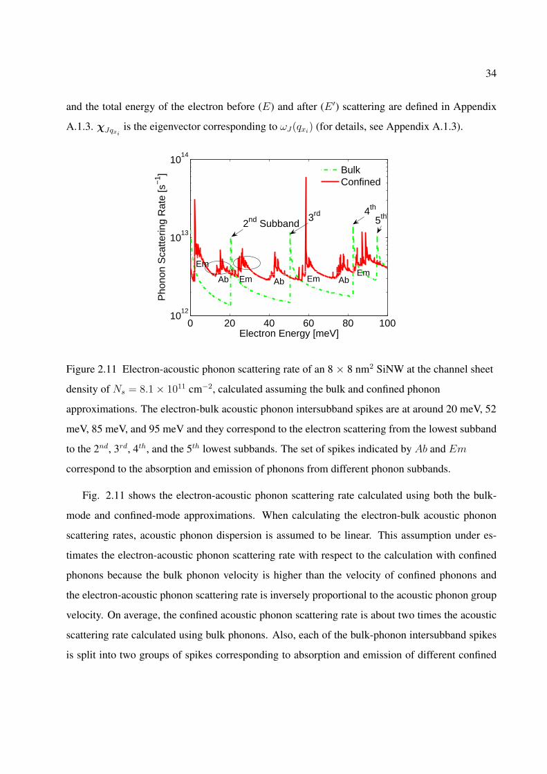
34
and the total energy of the electron before (E) and after (E ′) scattering are defined in Appendix
A.1.3. χJqxiis the eigenvector corresponding to ωJ(qxi
) (for details, see Appendix A.1.3).
0 20 40 60 80 10010
12
1013
1014
Electron Energy [meV]
Pho
non
Sca
tterin
g R
ate
[s−
1 ] BulkConfined
2nd Subband4th
3rd5th
Ab Em Em
EmEm
Ab Ab
Figure 2.11 Electron-acoustic phonon scattering rate of an 8 × 8 nm2 SiNW at the channel sheet
density of Ns = 8.1× 1011 cm−2, calculated assuming the bulk and confined phonon
approximations. The electron-bulk acoustic phonon intersubband spikes are at around 20 meV, 52
meV, 85 meV, and 95 meV and they correspond to the electron scattering from the lowest subband
to the 2nd, 3rd, 4th, and the 5th lowest subbands. The set of spikes indicated by Ab and Em
correspond to the absorption and emission of phonons from different phonon subbands.
Fig. 2.11 shows the electron-acoustic phonon scattering rate calculated using both the bulk-
mode and confined-mode approximations. When calculating the electron-bulk acoustic phonon
scattering rates, acoustic phonon dispersion is assumed to be linear. This assumption under es-
timates the electron-acoustic phonon scattering rate with respect to the calculation with confined
phonons because the bulk phonon velocity is higher than the velocity of confined phonons and
the electron-acoustic phonon scattering rate is inversely proportional to the acoustic phonon group
velocity. On average, the confined acoustic phonon scattering rate is about two times the acoustic
scattering rate calculated using bulk phonons. Also, each of the bulk-phonon intersubband spikes
is split into two groups of spikes corresponding to absorption and emission of different confined
35
phonon modes. In order to account for both intrasuband and intersubband transitions, all the four
sets of acoustic phonon modes are included in the calculation of the confined acoustic phonon-
electron scattering rates. But, it should be noted that the dominant contribution to the scattering
rate comes from the dilatational modes (for all other sets of modes the overlap integral Lnm(J, qx)
in Eq.(2.9) vanishes for intrasubband scattering due to their symmetry).
2.2.6 Electron Mobility in SiNWs Revisited: The role of acoustic phonon con-finement and surface roughness scattering
In this section, we emphasize the importance of acoustic phonon confinement in SiNWs, and
then vary the cross section of the wire to investigate the effect of increasing spatial confinement on
electron mobility. SRS overlap integral given by Eq. (2.6) is used to calculate the SRS to account
for the finite thickness and width of the wire.
The electron mobility in an 8 × 8 nm2 wire, with and without phonon confinement, is shown
in Fig. 2.12. In the low transverse field regime, the mobility calculated with confined acoustic
phonons is about 10 % smaller than that obtained with bulk phonons. This clearly indicates that
confined acoustic phonons need to be properly included in the study of electrical transport in
SiNWs. The mobility values for 8 × 8 nm2 are very close to the experimentally observed mobility
in an ultra-thin SOI of similar thickness [88]. In the rest of the article the acoustic phonons are
treated under confined mode approximation.
To determine the cross sectional dependence of electron mobility in SiNWs and to understand
the confinement effects on the spatial and k-space distribution of electrons, the cross section of
the wire was varied from 8 × 8 nm2 to 3 × 3 nm2. The variation of the electron mobility with
decreasing wire cross section at a low (1.4 ×10⁻² MV/cm), moderate (2.4 ×10⁻¹ MV/cm) and
high (1.04 MV/cm) transverse field is are plotted in Fig. 2.13.
2.2.6.1 Subband Modulation
One of the most important factors that determine the energy and occupation probability of a
subband in each of the ∆6 valleys (equivalent in bulk silicon) is the effective mass in the direction
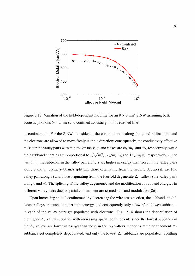
36
10−2
10−1
100
300
400
500
600
700
Effective Field [MV/cm]
Ele
ctro
n M
obili
ty [c
m2 /V
s]
ConfinedBulk
Figure 2.12 Variation of the field-dependent mobility for an 8 × 8 nm2 SiNW assuming bulk
acoustic phonons (solid line) and confined acoustic phonons (dashed line).
of confinement. For the SiNWs considered, the confinement is along the y and z directions and
the electrons are allowed to move freely in the x direction; consequently, the conductivity effective
mass for the valley pairs with minima on the x, y, and z axes are ml,mt, and mt, respectively, while
their subband energies are proportional to 1/√
m2t , 1/
√mtml, and 1/
√mtml, respectively. Since
mt < ml, the subbands in the valley pair along x are higher in energy than those in the valley pairs
along y and z. So the subbands split into those originating from the twofold degenerate ∆2 (the
valley pair along x) and those originating from the fourfold degenerate ∆4 valleys (the valley pairs
along y and z). The splitting of the valley degeneracy and the modification of subband energies in
different valley pairs due to spatial confinement are termed subband modulation [86].
Upon increasing spatial confinement by decreasing the wire cross section, the subbands in dif-
ferent valleys are pushed higher up in energy, and consequently only a few of the lowest subbands
in each of the valley pairs get populated with electrons. Fig. 2.14 shows the depopulation of
the higher ∆2 valley subbands with increasing spatial confinement: since the lowest subbands in
the ∆4 valleys are lower in energy than those in the ∆2 valleys, under extreme confinement ∆2
subbands get completely depopulated, and only the lowest ∆4 subbands are populated. Splitting
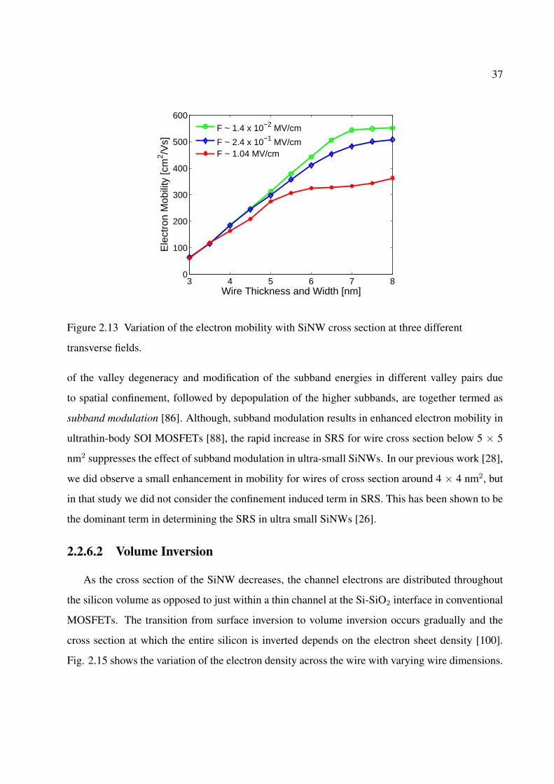
37
3 4 5 6 7 80
100
200
300
400
500
600
Wire Thickness and Width [nm]
Ele
ctro
n M
obili
ty [c
m2 /V
s]
F ~ 1.4 x 10⁻² MV/cm
F ~ 2.4 x 10⁻¹ MV/cmF ~ 1.04 MV/cm
Figure 2.13 Variation of the electron mobility with SiNW cross section at three different
transverse fields.
of the valley degeneracy and modification of the subband energies in different valley pairs due
to spatial confinement, followed by depopulation of the higher subbands, are together termed as
subband modulation [86]. Although, subband modulation results in enhanced electron mobility in
ultrathin-body SOI MOSFETs [88], the rapid increase in SRS for wire cross section below 5 × 5
nm2 suppresses the effect of subband modulation in ultra-small SiNWs. In our previous work [28],
we did observe a small enhancement in mobility for wires of cross section around 4 × 4 nm2, but
in that study we did not consider the confinement induced term in SRS. This has been shown to be
the dominant term in determining the SRS in ultra small SiNWs [26].
2.2.6.2 Volume Inversion
As the cross section of the SiNW decreases, the channel electrons are distributed throughout
the silicon volume as opposed to just within a thin channel at the Si-SiO2 interface in conventional
MOSFETs. The transition from surface inversion to volume inversion occurs gradually and the
cross section at which the entire silicon is inverted depends on the electron sheet density [100].
Fig. 2.15 shows the variation of the electron density across the wire with varying wire dimensions.
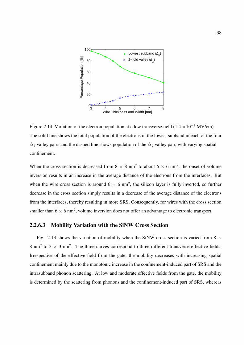
38
3 4 5 6 7 80
20
40
60
80
100
Wire Thickness and Width [nm]
Per
cent
age
Pop
ulat
ion
[%]
Lowest subband (∆4)
2−fold valley (∆2)
Figure 2.14 Variation of the electron population at a low transverse field (1.4 ×10⁻² MV/cm).
The solid line shows the total population of the electrons in the lowest subband in each of the four
∆4 valley pairs and the dashed line shows population of the ∆2 valley pair, with varying spatial
confinement.
When the cross section is decreased from 8 × 8 nm2 to about 6 × 6 nm2, the onset of volume
inversion results in an increase in the average distance of the electrons from the interfaces. But
when the wire cross section is around 6 × 6 nm2, the silicon layer is fully inverted, so further
decrease in the cross section simply results in a decrease of the average distance of the electrons
from the interfaces, thereby resulting in more SRS. Consequently, for wires with the cross section
smaller than 6 × 6 nm2, volume inversion does not offer an advantage to electronic transport.
2.2.6.3 Mobility Variation with the SiNW Cross Section
Fig. 2.13 shows the variation of mobility when the SiNW cross section is varied from 8 ×8 nm2 to 3 × 3 nm2. The three curves correspond to three different transverse effective fields.
Irrespective of the effective field from the gate, the mobility decreases with increasing spatial
confinement mainly due to the monotonic increase in the confinement-induced part of SRS and the
intrasubband phonon scattering. At low and moderate effective fields from the gate, the mobility
is determined by the scattering from phonons and the confinement-induced part of SRS, whereas
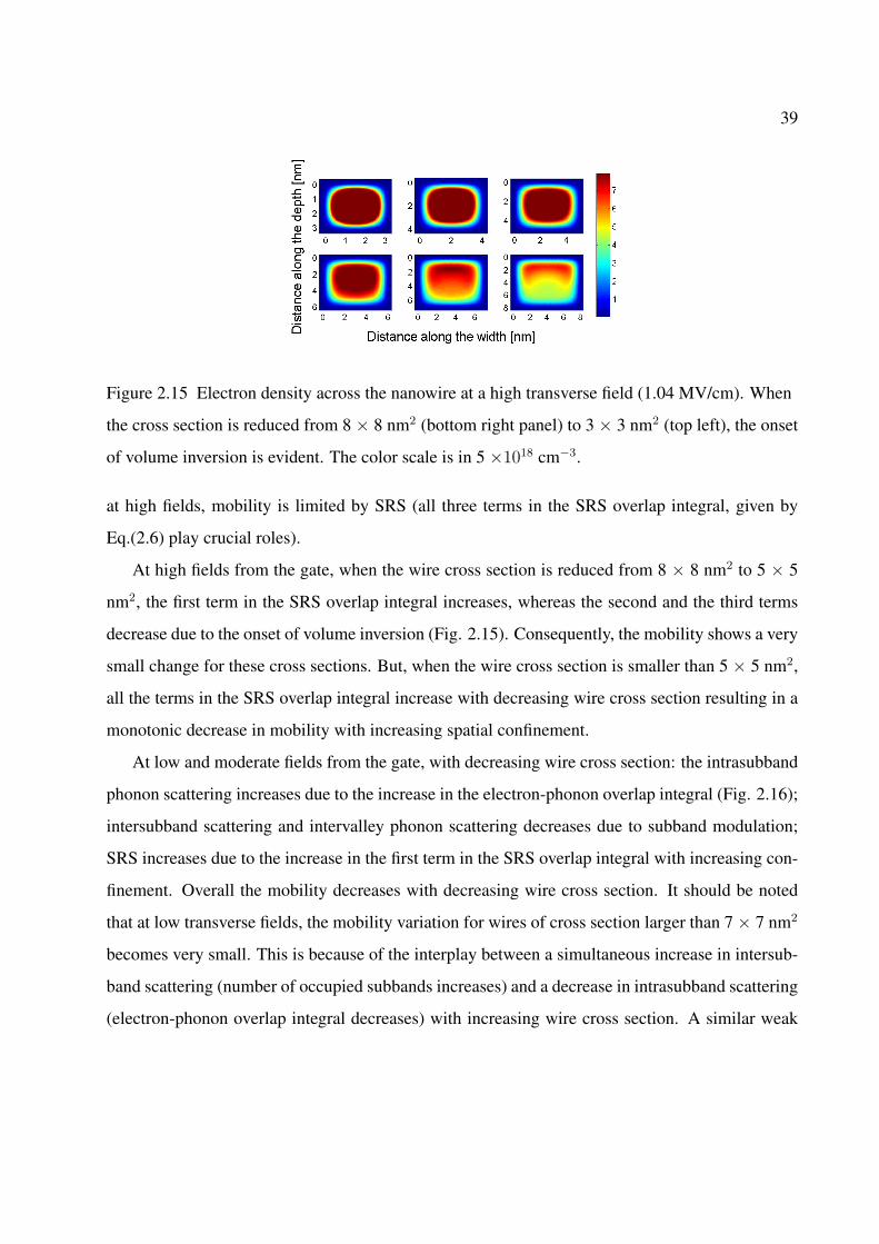
39
Figure 2.15 Electron density across the nanowire at a high transverse field (1.04 MV/cm). When
the cross section is reduced from 8 × 8 nm2 (bottom right panel) to 3 × 3 nm2 (top left), the onset
of volume inversion is evident. The color scale is in 5 ×1018 cm−3.
at high fields, mobility is limited by SRS (all three terms in the SRS overlap integral, given by
Eq.(2.6) play crucial roles).
At high fields from the gate, when the wire cross section is reduced from 8 × 8 nm2 to 5 × 5
nm2, the first term in the SRS overlap integral increases, whereas the second and the third terms
decrease due to the onset of volume inversion (Fig. 2.15). Consequently, the mobility shows a very
small change for these cross sections. But, when the wire cross section is smaller than 5 × 5 nm2,
all the terms in the SRS overlap integral increase with decreasing wire cross section resulting in a
monotonic decrease in mobility with increasing spatial confinement.
At low and moderate fields from the gate, with decreasing wire cross section: the intrasubband
phonon scattering increases due to the increase in the electron-phonon overlap integral (Fig. 2.16);
intersubband scattering and intervalley phonon scattering decreases due to subband modulation;
SRS increases due to the increase in the first term in the SRS overlap integral with increasing con-
finement. Overall the mobility decreases with decreasing wire cross section. It should be noted
that at low transverse fields, the mobility variation for wires of cross section larger than 7 × 7 nm2
becomes very small. This is because of the interplay between a simultaneous increase in intersub-
band scattering (number of occupied subbands increases) and a decrease in intrasubband scattering
(electron-phonon overlap integral decreases) with increasing wire cross section. A similar weak
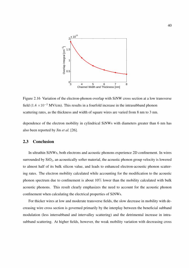
40
3 4 5 6 7 80
0.5
1
1.5
2x 10
13
Channel Width and Thickness [nm]
Ove
rlap
Inte
gral
[cm
−2 ]
Figure 2.16 Variation of the electron-phonon overlap with SiNW cross section at a low transverse
field (1.4 ×10⁻² MV/cm). This results in a fourfold increase in the intrasubband phonon
scattering rates, as the thickness and width of square wires are varied from 8 nm to 3 nm.
dependence of the electron mobility in cylindrical SiNWs with diameters greater than 6 nm has
also been reported by Jin et al. [26].
2.3 Conclusion
In ultrathin SiNWs, both electrons and acoustic phonons experience 2D confinement. In wires
surrounded by SiO2, an acoustically softer material, the acoustic phonon group velocity is lowered
to almost half of its bulk silicon value, and leads to enhanced electron-acoustic phonon scatter-
ing rates. The electron mobility calculated while accounting for the modification to the acoustic
phonon spectrum due to confinement is about 10% lower than the mobility calculated with bulk
acoustic phonons. This result clearly emphasizes the need to account for the acoustic phonon
confinement when calculating the electrical properties of SiNWs.
For thicker wires at low and moderate transverse fields, the slow decrease in mobility with de-
creasing wire cross section is governed primarily by the interplay between the beneficial subband
modulation (less intersubband and intervalley scattering) and the detrimental increase in intra-
subband scattering. At higher fields, however, the weak mobility variation with decreasing cross
41
section stems from the competing influences of the beneficial volume inversion and the detrimental
enhancement of the confinement-induced SRS term.
For very thin wires (below the 5×5 nm2 cross section), the mobility decreases monotonically
with increasing spatial confinement and becomes virtually independent of the transverse electric
field. This occurs primarily due to the increase in the field-independent, confinement-induced
part of the SRS in Eq.(2.6), and second due to the increase in intrasubband phonon scattering.
In contrast to bulk MOSFETs, in which the SRS plays an important role only for high fields
from the gate, electrons in very thin SiNWs are strongly influenced by the roughness regardless
of the transverse field. This finding is important both for FETs with multiple gates, such as the
FinFET [101], as well as for ungated ultrathin wires used for TE applications [5] or interconnects.
42
Chapter 3
Thermoelectric Figure of Merit
The thermoelectric coefficients required to calculate ZT in a material can be derived from
the electron and phonon BTE [18,19]. Previous theoretical studies of ZT [5,102] in wires assume
extreme quantum limit and a constant relaxation time (obtained from the bulk mobility) to calculate
the electronic coefficients such as the electronic contribution to the Seebeck Coefficient (Se), the
electronic contribution to the thermal conductivity (κe), and the electrical conductivity (σ). But, as
indicated in the previous chapter, none of these assumptions are valid for the wire cross sections
considered in this study. As for the phononic thermal conductivity (κl) calculation in NWs, two
distinct approaches have been employed: one is to solve the Boltzmann transport equation (BTE)
for phonons, and the other is to employ molecular dynamics (MD) simulations.
3.1 Derivation of Electronic Coefficients in ZT
The expressions required to calculate the electronic contribution to the Seebeck coefficient,
thermal conductivity, and electrical conductivity can be derived from the 1D electron BTE (follow-
ing the procedure used in the calculation of these coefficients in bulk semiconductors [18, 103]).
In steady state, the BTE for electrons in subband n of valley ν in the RTA is given by
f νn(E)− f ν
n0(E)
τ νn (E)
= −kx∂f ν
n(E)
∂kx
− x∂f ν
n(E)
∂x, (3.1)
where f νn0(E) and f ν
n(E) represent the unperturbed (equilibrium Fermi function) and perturbed
electron distribution functions, respectively. kx and x are the wavevector and position of electron
and the dots above these indicate the partial derivative with respect to time. τ νn (E) is the relaxation
time for an electron with kinetic energy E . Assuming low field (both electrical and thermal),
43
|f νn(E) − f ν
n0(E)| << f νn0(E), therefore f ν
n(E) on the rhs of Eq. (3.1) can be replaced by f νn0(E).
Also, by accounting for the dependence of the Fermi distribution function on displacement through
both the electric field and thermal gradient, the electron BTE can be rewritten as
f νn(E)− f ν
n0(E)
τ νn (E)
= υνn(E)
∂f νn0(E)
∂E[∂EF
∂x+Eν
n + E − EF
T
∂T
∂x
], (3.2)
where υνn(E) is the velocity of the electron in x direction, EF is the Fermi level, Eν
n is the subband
energy, and T is the temperature.
The electronic contribution to the Seebeck coefficient and the thermal conductivity are calcu-
lated from the electrical current density and the rate of heat flow in wires. The electrical current
density is given by
j = − e
Ω
∑
kx
υνn(E)f ν
n(E), (3.3)
where e is the electron charge magnitude and Ω = LWH is the volume of the SiNW of cross
section W ×H and length L.
Substituting f νn(E) from Eq. (3.2) in Eq. (3.3), we get
j = − e
Ω
∑
kx
[υνn(E)]2τ ν
n (E)∂f ν
n0(E)
∂(E)
[∂EF
∂x+En + E − EF
T
∂T
∂x
]. (3.4)
Converting the sum over kx to integral over E , the above equation can be expressed as
j = − 2√
2e
πhWH√
mν
∫dE√Eτ ν
n (E)∂f ν
n0(E)
∂(E)
[∂EF
∂x+En + E − EF
T
∂T
∂x
]. (3.5)
Since the energy carried by each electron is En + E − EF , the rate of heat flow is given by
w =1
Ω
∑
kx
υνn(E)[En + E − EF ]f ν
n(E). (3.6)
Substituting f νn(E) from Eq. (3.2) and converting the sum over k to integral over E as in the
calculation of the current density, the rate of heat flow can be rewritten as
w =2√
2
πhWH√
mν
∫dE√E [En + E − EF ]τ ν
n (E)∂f ν
n0(E)
∂E[∂EF
∂x+En + E − EF
T
∂T
∂x
]. (3.7)
The electronic contributions to the Seebeck coefficient and the lattice thermal conductivity are
defined at zero current. The Seebeck coefficient is defined as limx→0
∆V∆T
, where ∆V is the voltage
44
difference observed due to a temperature difference ∆T . In terms of the temperature gradient and
electric field F, it can be written as
Se =F
∇T=
∂EF
∂x
[e∂T
∂x
]−1
. (3.8)
By setting j = 0 in Eq. (3.5) and using the above expression, the electronic contribution to the
Seebeck coefficient, accounting for all the subbands and valleys, is
κe =1
eT
[EF −
∑ν,n
∫dE √E [En + E ]
∂fνn0(E)
∂E τ νn (E)∫
dE √E ∂fνn0(E)
∂E τ νn (E)
]. (3.9)
The electronic contribution to the lattice thermal conductivity relates the temperature gradient
to the heat flow resulting from it. It is given by
κe = −w
[∂T
∂x
]−1
. (3.10)
By substituting ∂EF /∂x from Eq. (3.5) for j = 0 in Eq. (3.7) and using the above expression,
the electronic contribution to the thermal conductivity accounting for all the subbands and valleys
is
Se =2√
2
πhWH√
mT
∑ν,n
∫dE √E [En + E ]
∂fνn0(E)
∂E τ νn (E)
2
∫dE √E ∂fν
n0(E)
∂E τ νn (E)
−∫
dE√E [En + E ]2
∂f νn0(E)
∂E τ νn (E)
.
(3.11)
3.2 Electrical Conductivity
Electrical conductivity of a material is defined as the ratio of the electrical current density to the
electric field which drives that current in the absence of a thermal gradient. In terms of the mobility
(µ) of the carriers (electrons or holes) and the charge density (ne), the electrical conductivity can
be written as σ = neµ. The electron transport simulator described in the previous chapter is used
to calculate the electrical conductivity.
The electronic bandstructure in SiNWs is altered from that of bulk silicon due to 2D confine-
ment [52,53,58,104]. This effect is included through the effective mass and the bandgap variation
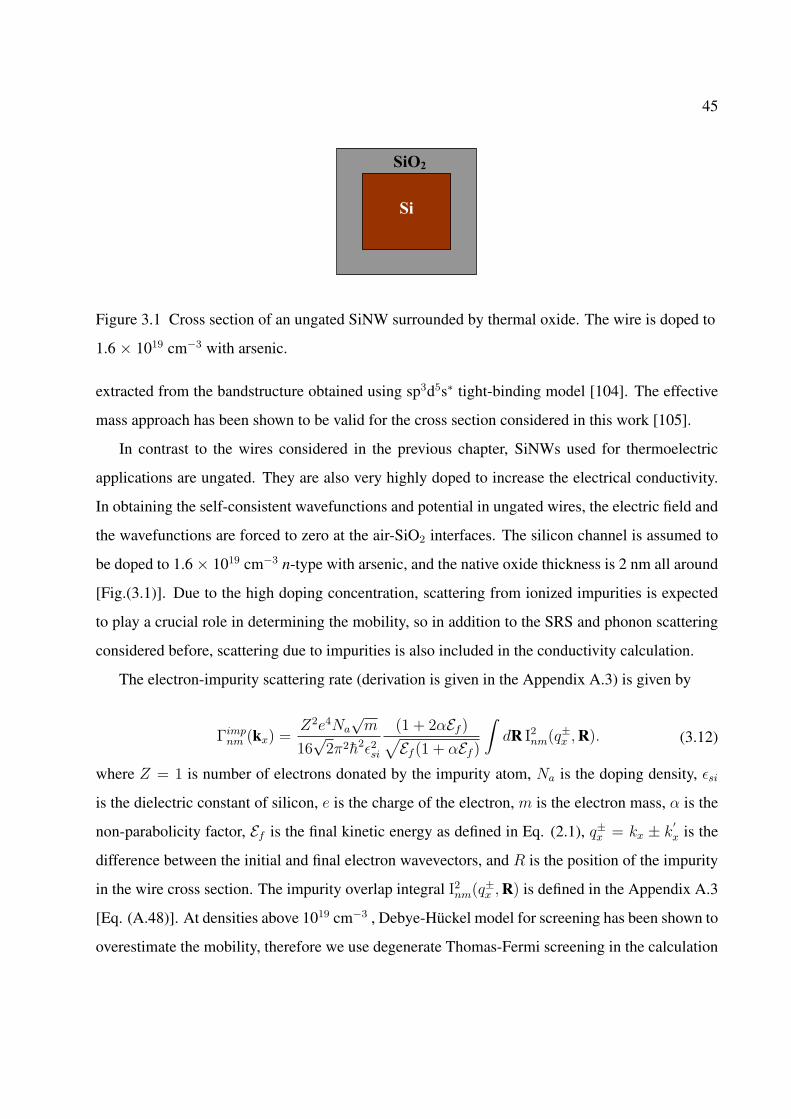
45
Si
SiO2
Figure 3.1 Cross section of an ungated SiNW surrounded by thermal oxide. The wire is doped to
1.6 × 1019 cm−3 with arsenic.
extracted from the bandstructure obtained using sp3d5s∗ tight-binding model [104]. The effective
mass approach has been shown to be valid for the cross section considered in this work [105].
In contrast to the wires considered in the previous chapter, SiNWs used for thermoelectric
applications are ungated. They are also very highly doped to increase the electrical conductivity.
In obtaining the self-consistent wavefunctions and potential in ungated wires, the electric field and
the wavefunctions are forced to zero at the air-SiO2 interfaces. The silicon channel is assumed to
be doped to 1.6× 1019 cm−3 n-type with arsenic, and the native oxide thickness is 2 nm all around
[Fig.(3.1)]. Due to the high doping concentration, scattering from ionized impurities is expected
to play a crucial role in determining the mobility, so in addition to the SRS and phonon scattering
considered before, scattering due to impurities is also included in the conductivity calculation.
The electron-impurity scattering rate (derivation is given in the Appendix A.3) is given by
Γimpnm (kx) =
Z2e4Na
√m
16√
2π2h2ε2si
(1 + 2αEf )√Ef (1 + αEf )
∫dR I2nm(q±x , R). (3.12)
where Z = 1 is number of electrons donated by the impurity atom, Na is the doping density, εsi
is the dielectric constant of silicon, e is the charge of the electron, m is the electron mass, α is the
non-parabolicity factor, Ef is the final kinetic energy as defined in Eq. (2.1), q±x = kx ± k′x is the
difference between the initial and final electron wavevectors, and R is the position of the impurity
in the wire cross section. The impurity overlap integral I2nm(q±x , R) is defined in the Appendix A.3
[Eq. (A.48)]. At densities above 1019 cm−3 , Debye-Huckel model for screening has been shown to
overestimate the mobility, therefore we use degenerate Thomas-Fermi screening in the calculation
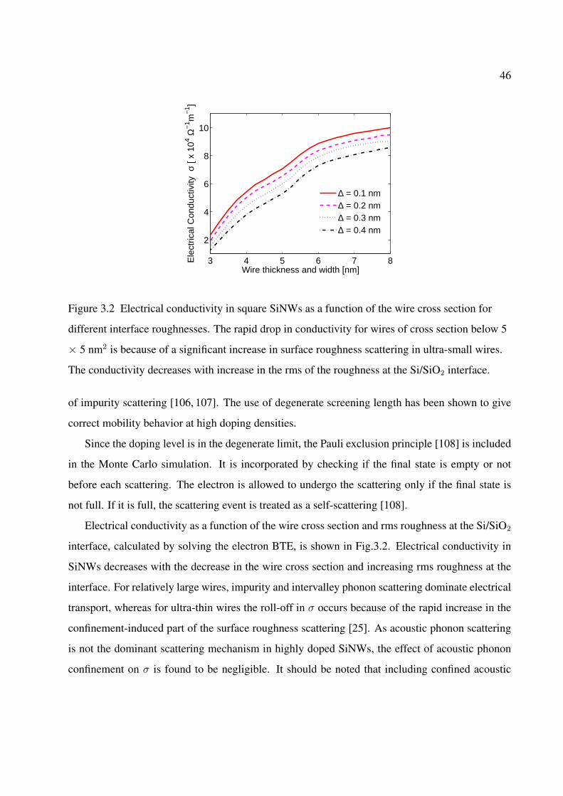
46
3 4 5 6 7 8
2
4
6
8
10
Wire thickness and width [nm]
Ele
ctric
al C
ondu
ctiv
ity σ
[ x
104 Ω
−1 m
−1 ]
∆ = 0.1 nm∆ = 0.2 nm∆ = 0.3 nm∆ = 0.4 nm
Figure 3.2 Electrical conductivity in square SiNWs as a function of the wire cross section for
different interface roughnesses. The rapid drop in conductivity for wires of cross section below 5
× 5 nm2 is because of a significant increase in surface roughness scattering in ultra-small wires.
The conductivity decreases with increase in the rms of the roughness at the Si/SiO2 interface.
of impurity scattering [106, 107]. The use of degenerate screening length has been shown to give
correct mobility behavior at high doping densities.
Since the doping level is in the degenerate limit, the Pauli exclusion principle [108] is included
in the Monte Carlo simulation. It is incorporated by checking if the final state is empty or not
before each scattering. The electron is allowed to undergo the scattering only if the final state is
not full. If it is full, the scattering event is treated as a self-scattering [108].
Electrical conductivity as a function of the wire cross section and rms roughness at the Si/SiO2
interface, calculated by solving the electron BTE, is shown in Fig.3.2. Electrical conductivity in
SiNWs decreases with the decrease in the wire cross section and increasing rms roughness at the
interface. For relatively large wires, impurity and intervalley phonon scattering dominate electrical
transport, whereas for ultra-thin wires the roll-off in σ occurs because of the rapid increase in the
confinement-induced part of the surface roughness scattering [25]. As acoustic phonon scattering
is not the dominant scattering mechanism in highly doped SiNWs, the effect of acoustic phonon
confinement on σ is found to be negligible. It should be noted that including confined acoustic

47
phonons in mobility calculation resulted in an additional 10% degradation in the case of nearly-
undoped gated SiNWs [25].
3.3 Lattice Thermal Conductivity
Solving the phonon Boltzmann transport equation requires one to identify the dominant scat-
tering mechanism for phonons a priori. Then, the energy-resolved scattering rates for each of the
important scattering mechanisms are precalculated, and typically used within the relaxation-time
approximation [12, 21, 28, 78, 109, 110] (often referred to as the Klemens- Callaway [111, 112] or
just Callaway approach in the context of thermal transport). The phonon BTE was solved within
the relaxation-time approximation for Si and Ge nanowires by Mingo et al. [24], and good overall
agreement with experiment was obtained, but the cross-over in the temperature variation of the
thermal conductivity from T 3 to T was not addressed. Mingo et al. calculated κl from the 1D
phonon BTE instead of using the Klemens-Callaway expression (which was originally derived for
bulk semiconductors) and also accounted for the modification of acoustic phonon dispersion in
wires.
Alternatively, one can use the ensemble Monte Carlo (EMC) technique [113], a stochastic
method which directly generates the phonon distribution function, and is universally regarded as
the most accurate, versatile, and robust way to solve the Boltzmann transport equation (the EMC
coincides with the solution of BTE in the long-time limit). The EMC simulation of phonon trans-
port in bulk semiconductors and thick nanowires (above about 30 nm) has shown good agreement
with experimentally observed κl [23, 114]. One major advantage of the EMC is that it can be used
to study the time-resolved heat transfer through Si nanowires. Until now, no attempt has been
made to include the modified acoustic phonon dispersion in the calculation of κl using the EMC
(phonon scattering corresponding to bulk silicon is typically used). This could be the reason why
the EMC simulation has not yet been able to match κl for the wires of cross section smaller than
30 nm.
In a molecular dynamics (MD) simulation, atoms bound in the solid obey classical laws of
motion. There are two variants of the MD technique used for phonon transport: the equilibrium
48
MD, based on the Green-Kubo formula that connects the equilibrium value of the current-current
correlation function to thermal conductivity (see, e.g., Ref. [115] and references therein), and the
nonequilibrium (or direct) MD, where κl is obtained from the thermal gradient and the heat cur-
rent directly. However, finite size effects have different effects on the two methods [116, 117].
On the upside, the molecular dynamics approach requires no assumptions on the nature of scat-
tering mechanisms that dominate phonon transport. However, the method is very computationally
intensive and depends critically on the choice of interatomic potentials. Often, empirical poten-
tials are utilized (such as the Tersoff potential [118]), as the more realistic tight-binding ones are
too computationally demanding. The MD approach is useful for very thin layers [119], ultrathin
nanowires [120,121], and zero-dimensional structures with features no greater than a few nanome-
ters. Major downside of MD approaches is the limit on the structure size. So far, MD results have
typically been reported for wires of diameter in the 2-4 nm range, very challenging to produce and
control.
Nonequilibrium MD simulations were performed on thin Si nanowires [122], ZnO nanowires
[123], SiC nanowires [124], as well as ultrathin Si films [119] and GaN nanotubes [124]. A Cal-
tech group lead by Goddard performed equilibrium (Green-Kubo) simulations to find the thermal
conductivity of bulk diamond [125], and recently to analyze thermal transport in SiNWs [17].
Here, the lattice thermal conductivity is calculated by solving the phonon BTE using three dif-
ferent approaches: (a). The Klemens-Callaway method, modified to include the acoustic phonon
confinement; (b). solving the 1D phonon BTE under relaxation time approximation; (c). solving
the phonon BTE using the Monte Carlo technique. Among these three approaches, the MC tech-
nique has been found to be the most appropriate one for the calculation of κl in rough SiNWs and
will be discussed in detail in Section 3.3.3. The flowchart of the simulator developed to solve the
phonon BTE and calculate κl is shown in Fig. 3.3. The electronic contribution to thermal con-
ductivity is calculated by solving the 1D electron BTE under the relaxation time approximation
(RTA).

49
Figure 3.3 Thermal simulator flowchart developed to solve the phonon Boltzmann equation.
3.3.1 Lattice Thermal Conductivity Using the Klemens-Callaway Method
The Klemens-Callaway expression for κl is obtained from the phonon BTE under the RTA. The
main advantage of using this kernel is that it can include the confined acoustic phonon spectrum
to an extent. The effect of confinement is included through the modified acoustic phonon group
velocity [Fig. (3.4)], which is calculated from the confined acoustic phonon dispersion using the
xyz algorithm [3]. When calculating the acoustic phonon group velocity, we have accounted for the
non-uniform energy gap between neighboring phononic bands, whereas previous studies [12, 21]
have used an average energy gap between phononic bands. This modification is very important,
because the energy gap between different phononic bands strongly depends on the wavevector of
the phonon. We have included the scattering of phonons due to other phonons, electrons, impuri-
ties, and boundaries (using a specularity parameter, α). κl for a SiNW with a square cross section
is given by [12]

50
0 2 4 6 8 10 12
2
4
6
8
10x 10
5
Acoustic phonon energy [meV]
Gro
up v
eloc
ity [c
m/s
] Sound velocityin bulk Si
Figure 3.4 Group velocity of dilatational modes for an 8 x 8 nm2 SiNW. On average, acoustic
phonon group velocity is reduced to less than 50 % of the bulk value (9.13 x 105 cm/s).
κl(T, a, α) =kB
2π2
(kBT
h
)3
×∫ θD/T
0
x4ex
(ex − 1)2
τ(x)
υ(x)L[γ(x), α]dx,
(3.13)
where x = hω/kBT , ω is the frequncy of the phonon, θD is the Debye temperature, γ(x) = a/Λ(x)
is the ratio the NW side length a and the phonon mean free path Λ(x) = υ(x)τ(x), υ is the acoustic
phonon group velocity averaged over all modes, τ(x) is the relaxation time of the acoustic phonon
due to three-phonon umklapp (τu), boundary scattering (τb), impurity scattering (τi), and electron
scattering (τe), and L defines the boundary scattering in NWs with square cross section. 0 ≤ α ≤ 1
is the fraction of specular reflection of phonons from the SiNW boundaries (α = 0 indicates fully
diffusive scattering). The expression for τu and τb were taken from Ref. [78] and τi and τe were
taken from Ref. [126] and Ref. [21], respectively. For M acoustic phonon modes, the averaged
group velocity is given by υ(x) = 1M
∑n υn(x).
The lattice thermal conductivity variation with the wire cross section with fully diffuse bound-
ary scattering is shown in Fig. 3.5. κl decreases almost linearly with decreasing wire cross section
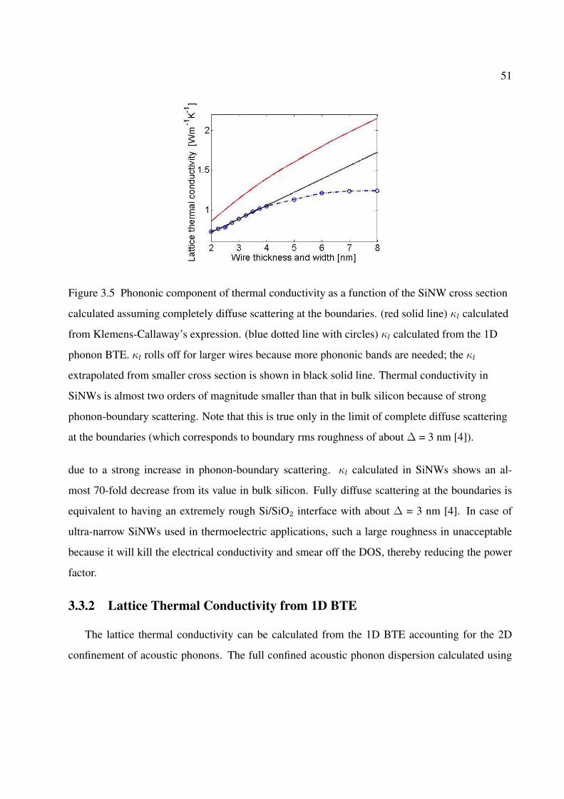
51
Figure 3.5 Phononic component of thermal conductivity as a function of the SiNW cross section
calculated assuming completely diffuse scattering at the boundaries. (red solid line) κl calculated
from Klemens-Callaway’s expression. (blue dotted line with circles) κl calculated from the 1D
phonon BTE. κl rolls off for larger wires because more phononic bands are needed; the κl
extrapolated from smaller cross section is shown in black solid line. Thermal conductivity in
SiNWs is almost two orders of magnitude smaller than that in bulk silicon because of strong
phonon-boundary scattering. Note that this is true only in the limit of complete diffuse scattering
at the boundaries (which corresponds to boundary rms roughness of about ∆ = 3 nm [4]).
due to a strong increase in phonon-boundary scattering. κl calculated in SiNWs shows an al-
most 70-fold decrease from its value in bulk silicon. Fully diffuse scattering at the boundaries is
equivalent to having an extremely rough Si/SiO2 interface with about ∆ = 3 nm [4]. In case of
ultra-narrow SiNWs used in thermoelectric applications, such a large roughness in unacceptable
because it will kill the electrical conductivity and smear off the DOS, thereby reducing the power
factor.
3.3.2 Lattice Thermal Conductivity from 1D BTE
The lattice thermal conductivity can be calculated from the 1D BTE accounting for the 2D
confinement of acoustic phonons. The full confined acoustic phonon dispersion calculated using

52
the xyz algorithm [3] is used in this calculation (instead of the modified group velocity in the
previous approach Section 3.3.1).
In steady state, the phonon Boltzmann transport equation can be written as(
∂Np(q)
∂t
)
drift
= −(
∂Np(q)
∂t
)
scat
, (3.14)
where Np(q) is the phonon distribution in the presence of scattering and the drift due to the applied
thermal gradient, while p is the phonon mode index. In the presence of the temperature gradient in
the x direction, the LHS of Eq. (3.14) becomes(
∂Np(q)
∂t
)
drift
= −υp(q)∂T
∂x
∂Np(q)
∂T, (3.15)
where υp(q) is the velocity of a phonon with wavevector q. In the relaxation-time approximation,
the change in the phonon distribution due to scattering is given by(
∂Np(q)
∂t
)
scat
=N0
p (q)−Np(q)
τp(q), (3.16)
where N0p (q) = 1/(ehωp(q)/KBT − 1) is the equilibrium phonon distribution at temperature T (the
Bose-Einstein distribution function), KB is the Boltzmann constant, ωn(q) is the frequency of
phonon with wavevector q, and τn(q) represents the combined phonon relaxation time due to their
scattering from other phonons, impurities, electrons, and the wire boundaries. Upon replacing
Np(q) by N0p (q) in Eq. (3.15), the phonon BTE under the RTA becomes
υp(q)∂T
∂x
∂N0p (q)
∂T=
N0p (q)−Np(q)
τp(q)(3.17)
The heat current carried by a phonon in the presence of a thermal gradient is given by
JQ =1
Ω
∑q,p
υp(q)hωp(q)Np(q). (3.18)
Using Np(q) from Eq. (3.17) in Eq.(3.18), and the Fourier relation between the heat current and
the thermal gradient JQ = −κl∂T/∂x, the lattice thermal conductivity can be written as
κl =1
Ω
∑q,p
υ2p(q)τp(q)hωp(q)
∂N0p (q)
∂T. (3.19)
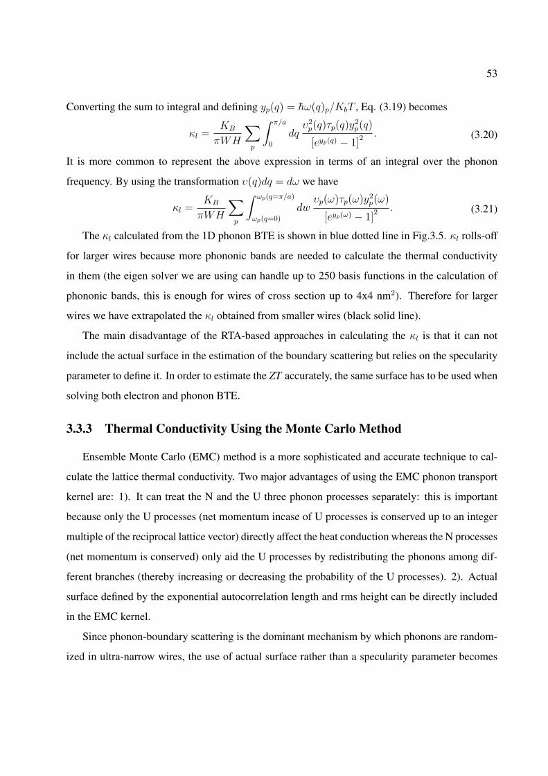
53
Converting the sum to integral and defining yp(q) = hω(q)p/KbT , Eq. (3.19) becomes
κl =KB
πWH
∑p
∫ π/a
0
dqυ2
p(q)τp(q)y2p(q)
[eyp(q) − 1]2 . (3.20)
It is more common to represent the above expression in terms of an integral over the phonon
frequency. By using the transformation υ(q)dq = dω we have
κl =KB
πWH
∑p
∫ ωp(q=π/a)
ωp(q=0)
dwυp(ω)τp(ω)y2
p(ω)
[eyp(ω) − 1]2 . (3.21)
The κl calculated from the 1D phonon BTE is shown in blue dotted line in Fig.3.5. κl rolls-off
for larger wires because more phononic bands are needed to calculate the thermal conductivity
in them (the eigen solver we are using can handle up to 250 basis functions in the calculation of
phononic bands, this is enough for wires of cross section up to 4x4 nm2). Therefore for larger
wires we have extrapolated the κl obtained from smaller wires (black solid line).
The main disadvantage of the RTA-based approaches in calculating the κl is that it can not
include the actual surface in the estimation of the boundary scattering but relies on the specularity
parameter to define it. In order to estimate the ZT accurately, the same surface has to be used when
solving both electron and phonon BTE.
3.3.3 Thermal Conductivity Using the Monte Carlo Method
Ensemble Monte Carlo (EMC) method is a more sophisticated and accurate technique to cal-
culate the lattice thermal conductivity. Two major advantages of using the EMC phonon transport
kernel are: 1). It can treat the N and the U three phonon processes separately: this is important
because only the U processes (net momentum incase of U processes is conserved up to an integer
multiple of the reciprocal lattice vector) directly affect the heat conduction whereas the N processes
(net momentum is conserved) only aid the U processes by redistributing the phonons among dif-
ferent branches (thereby increasing or decreasing the probability of the U processes). 2). Actual
surface defined by the exponential autocorrelation length and rms height can be directly included
in the EMC kernel.
Since phonon-boundary scattering is the dominant mechanism by which phonons are random-
ized in ultra-narrow wires, the use of actual surface rather than a specularity parameter becomes
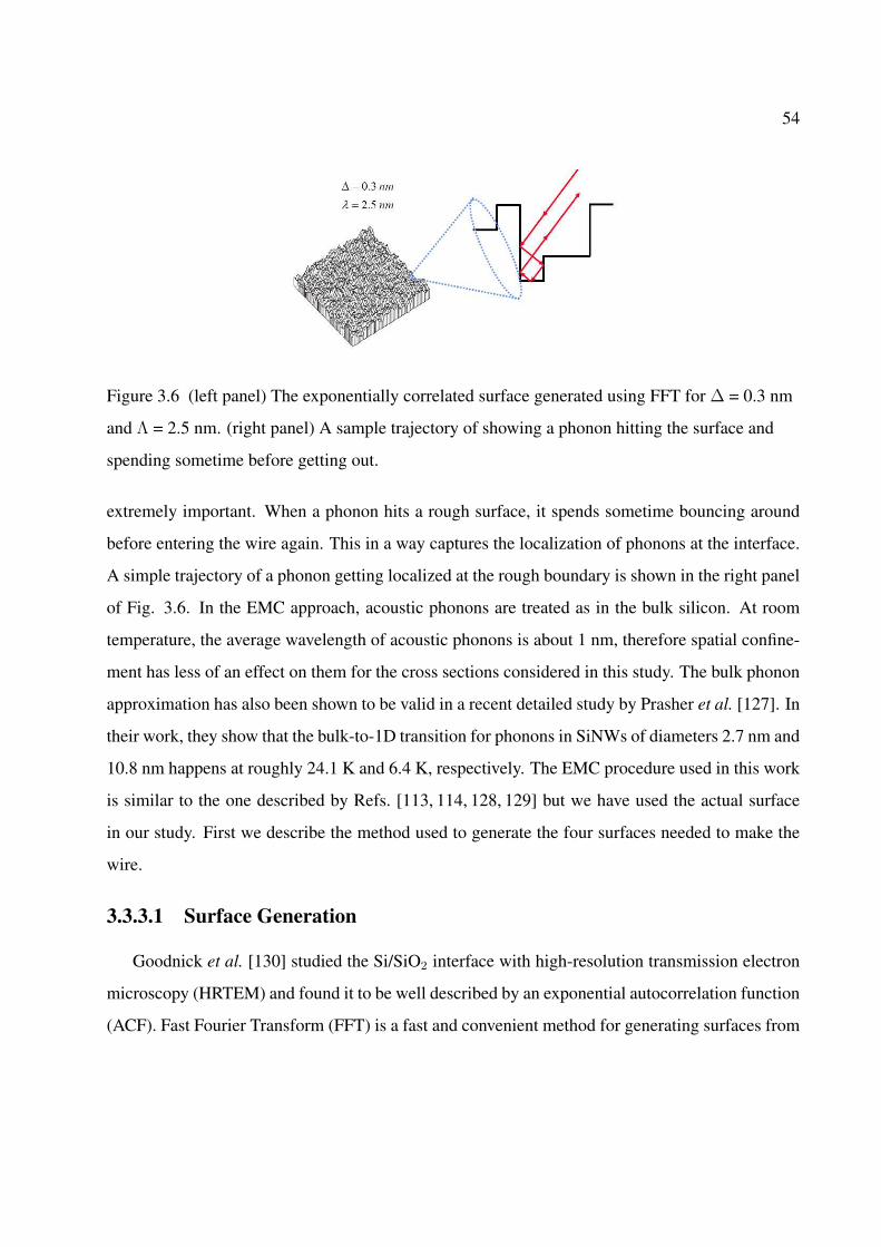
54
Figure 3.6 (left panel) The exponentially correlated surface generated using FFT for ∆ = 0.3 nm
and Λ = 2.5 nm. (right panel) A sample trajectory of showing a phonon hitting the surface and
spending sometime before getting out.
extremely important. When a phonon hits a rough surface, it spends sometime bouncing around
before entering the wire again. This in a way captures the localization of phonons at the interface.
A simple trajectory of a phonon getting localized at the rough boundary is shown in the right panel
of Fig. 3.6. In the EMC approach, acoustic phonons are treated as in the bulk silicon. At room
temperature, the average wavelength of acoustic phonons is about 1 nm, therefore spatial confine-
ment has less of an effect on them for the cross sections considered in this study. The bulk phonon
approximation has also been shown to be valid in a recent detailed study by Prasher et al. [127]. In
their work, they show that the bulk-to-1D transition for phonons in SiNWs of diameters 2.7 nm and
10.8 nm happens at roughly 24.1 K and 6.4 K, respectively. The EMC procedure used in this work
is similar to the one described by Refs. [113, 114, 128, 129] but we have used the actual surface
in our study. First we describe the method used to generate the four surfaces needed to make the
wire.
3.3.3.1 Surface Generation
Goodnick et al. [130] studied the Si/SiO2 interface with high-resolution transmission electron
microscopy (HRTEM) and found it to be well described by an exponential autocorrelation function
(ACF). Fast Fourier Transform (FFT) is a fast and convenient method for generating surfaces from
55
a given ACF. In this work we have adopted the method developed by Wu [131] to generate the
rough surface defined by rms ∆ and correlation length Λ. From a real ACF (Rr,s), an M×N
surface Zp,q can be generated by
Zp,q =M−1∑
k=0
N−1∑i=0
√Sk,iexp
(i2π
[φk,i +
kp
M+
iq
N
]), (3.22)
where p = 0, 1, 2, ..., (M − 1), q = 0, 1, 2, ..., (N − 1), Sk,i is the spectral density used to generate
the surface which is related to the ACF by Eq.(3.24), and φk,i are a set of independent random
phase angles distributed uniformly in the interval [0,2π]. In order to make Zp,q real, the following
restrictions are applied:
φk,i = −φM−k,N−i, k = 0, 1, 2, ..., M/2,
φk,0 = −φM−k,0, i = 0, 1, 2, ..., N/2,
φ0,i = −φ0,N−i,
φ0,0 = φ0,N/2 = φM/2,0 = φM/2,N/2 = 0;
(3.23)
Sk,i =1
MN
M−1∑r=0
N−1∑s=0
√Rr,sexp
(−i2π
[kr
M+
is
N
]),
k = 0, 1, 2, ..., (M − 1),
i = 0, 1, 2, ..., (N − 1).
(3.24)
From the given real ACF Rr,s, Rr,s is constructed by setting RN−r,M−s = Rr,M−s = RN−r,s =
Rr,s = Rr,s for all r = 0, 1, 2, ..., M/2 and s = 0, 1, 2, ..., N/2.
3.3.3.2 Initialization
The length of the wire is chosen such that it is much greater than the mean free path of phonons.
For the ultra-scaled wires considered in this study, the mean free path is less than 5 nm, therefore
we have set the length to be 200 nm. We find this length adequate to reach the diffuse limit i.e.
we do not see any discontinuity in the temperature profile at the contacts which is a signature of
ballistic transport (see Appendix C.1). The four surfaces of the wire are generated based on the

56
Figure 3.7 Schematic of a nanowire showing, the initial distribution of phonons: red and blue
dots indicate phonons at temperature 310 K and 290 K, respectively.
wire cross section. Then the wire is split up into 20 cells and phonons in them are initialized from
the equilibrium Bose-Einstein distribution.
The first and the last cells are treated as black bodies with a set high temperature TH and
low temperature TL, respectively. All the intermediate cells are set to the low temperature in the
beginning. The schematic of the nanowire showing the initial distribution of phonons is shown in
Fig. 3.7. The initialization of phonons involves three parts: Calculating the number of phonons in
the simulation domain; initializing phonon frequencies, wavevectors, and positions; setting up the
real-space boundary conditions.
Only acoustic phonons are included in the simulation because they are the dominant heat carri-
ers at room temperature. The dispersion of the TA (two-fold degenerate, gp = 2) and LA (gp = 1)
phonons in silicon in [100] direction has been approximated with a quadratic fit [6]. From the
dispersion and the Bose-Einstein distribution function, the number of phonons N in a volume V at
temperature T can be calculated.
N = V∑
p=LA,TA
Nw∑i=1
1
exp( hωi
KBT)− 1
q2i,p
2π2υi,p
gp∆ω, (3.25)
Nw is the number of spectral intervals between 0 and ωmaxLA with uniform spectral intervals ∆ω =
ωmaxLA /Nw. As the number of phonons N , even for a small volume of 10x10x10 nm3 at room
temperature, is about 105, a weighting factor Wt is used [128] in EMC calculation in order to
calculate the κl in a reasonable time. The number of simulated phonons is given by N = N/Wt.
Once the number of phonons that need to be simulated is calculated, the attributes of each phonon
are set.
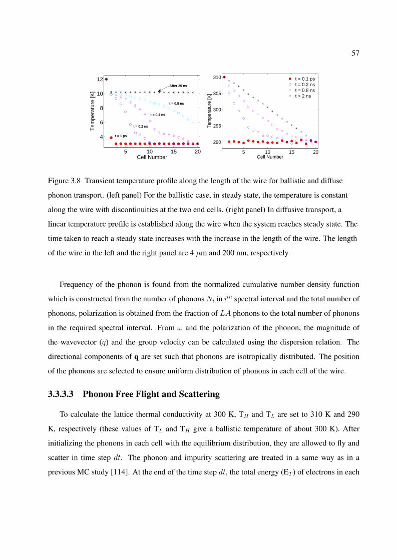
57
5 10 15 20
4
6
8
10
12
Cell Number
Tem
pera
ture
[K]
t = 1 ps
t = 0.2 ns
t = 0.4 ns
t = 0.8 ns
After 20 ns
5 10 15 20
290
295
300
305
310
Cell Number
Tem
pera
ture
[K]
t = 0.1 pst = 0.2 nst = 0.8 nst > 2 ns
Figure 3.8 Transient temperature profile along the length of the wire for ballistic and diffuse
phonon transport. (left panel) For the ballistic case, in steady state, the temperature is constant
along the wire with discontinuities at the two end cells. (right panel) In diffusive transport, a
linear temperature profile is established along the wire when the system reaches steady state. The
time taken to reach a steady state increases with the increase in the length of the wire. The length
of the wire in the left and the right panel are 4 µm and 200 nm, respectively.
Frequency of the phonon is found from the normalized cumulative number density function
which is constructed from the number of phonons Ni in ith spectral interval and the total number of
phonons, polarization is obtained from the fraction of LA phonons to the total number of phonons
in the required spectral interval. From ω and the polarization of the phonon, the magnitude of
the wavevector (q) and the group velocity can be calculated using the dispersion relation. The
directional components of q are set such that phonons are isotropically distributed. The position
of the phonons are selected to ensure uniform distribution of phonons in each cell of the wire.
3.3.3.3 Phonon Free Flight and Scattering
To calculate the lattice thermal conductivity at 300 K, TH and TL are set to 310 K and 290
K, respectively (these values of TL and TH give a ballistic temperature of about 300 K). After
initializing the phonons in each cell with the equilibrium distribution, they are allowed to fly and
scatter in time step dt. The phonon and impurity scattering are treated in a same way as in a
previous MC study [114]. At the end of the time step dt, the total energy (ET ) of electrons in each
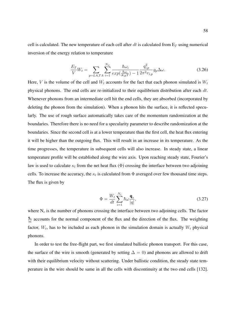
58
cell is calculated. The new temperature of each cell after dt is calculated from ET using numerical
inversion of the energy relation to temperature
ET
VWt =
∑p=LA,TA
Nw∑i=1
hωi
exp( hωi
KBT)− 1
q2i,p
2π2υi,p
gp∆ω. (3.26)
Here, V is the volume of the cell and Wt accounts for the fact that each phonon simulated is Wt
physical phonons. The end cells are re-initialized to their equilibrium distribution after each dt.
Whenever phonons from an intermediate cell hit the end cells, they are absorbed (incorporated by
deleting the phonon from the simulation). When a phonon hits the surface, it is reflected specu-
larly. The use of rough surface automatically takes care of the momentum randomization at the
boundaries. Therefore there is no need for a specularity parameter to describe randomization at the
boundaries. Since the second cell is at a lower temperature than the first cell, the heat flux entering
it will be higher than the outgoing flux. This will result in an increase in its temperature. As the
time progresses, the temperature in subsequent cells will also increase. In steady state, a linear
temperature profile will be established along the wire axis. Upon reaching steady state, Fourier’s
law is used to calculate κl from the net heat flux (Φ) crossing the interface between two adjoining
cells. To increase the accuracy, the κl is calculated from Φ averaged over few thousand time steps.
The flux is given by
Φ =Wt
dt
Nc∑i=1
hωqz
|q| , (3.27)
where Nc is the number of phonons crossing the interface between two adjoining cells. The factorqz
|q| accounts for the normal component of the flux and the direction of the flux. The weighting
factor, Wt, has to be included as each phonon in the simulation domain is actually Wt physical
phonons.
In order to test the free-flight part, we first simulated ballistic phonon transport. For this case,
the surface of the wire is smooth (generated by setting ∆ = 0) and phonons are allowed to drift
with their equilibrium velocity without scattering. Under ballistic condition, the steady state tem-
perature in the wire should be same in all the cells with discontinuity at the two end cells [132].
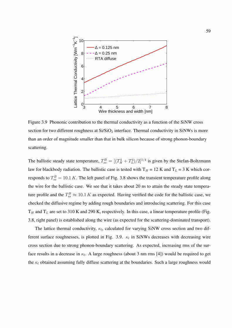
59
3 4 5 6 7 80
2
4
6
8
10
Wire thickness and width [nm]
Latti
ce T
herm
al C
ondu
ctiv
ity [W
m−
1 K−
1 ]
∆ = 0.125 nm∆ = 0.25 nmRTA diffuse
Figure 3.9 Phononic contribution to the thermal conductivity as a function of the SiNW cross
section for two different roughness at Si/SiO2 interface. Thermal conductivity in SiNWs is more
than an order of magnitude smaller than that in bulk silicon because of strong phonon-boundary
scattering.
The ballistic steady state temperature, TBss = [(T 4
H + T 4L)/2]1/4 is given by the Stefan-Boltzmann
law for blackbody radiation. The ballistic case is tested with TH = 12 K and TL = 3 K which cor-
responds to TBss = 10.1 K. The left panel of Fig. 3.8 shows the transient temperature profile along
the wire for the ballistic case. We see that it takes about 20 ns to attain the steady state tempera-
ture profile and the TBss ≈ 10.1 K as expected. Having verified the code for the ballistic case, we
checked the diffusive regime by adding rough boundaries and introducing scattering. For this case
TH and TL are set to 310 K and 290 K, respectively. In this case, a linear temperature profile (Fig.
3.8, right panel) is established along the wire (as expected for the scattering-dominated transport).
The lattice thermal conductivity, κl, calculated for varying SiNW cross section and two dif-
ferent surface roughnesses, is plotted in Fig. 3.9. κl in SiNWs decreases with decreasing wire
cross section due to strong phonon-boundary scattering. As expected, increasing rms of the sur-
face results in a decrease in κl. A large roughness (about 3 nm rms [4]) would be required to get
the κl obtained assuming fully diffuse scattering at the boundaries. Such a large roughness would
60
3 4 5 6 7 80
0.1
0.2
0.3
0.4
0.5
Wire thickness and width [nm]
κ e [Wm
−1 K
−1 ]
∆ = 0.1 nm∆ = 0.2 nm∆ = 0.3 nm∆ = 0.4 nm
Figure 3.10 Electronic contribution to thermal conductivity as a function of the SiNW cross
section for different roughness at Si/SiO2 interface. κe follows the same trend as σ variation with
cross section and roughness. As in bulk silicon, κe is smaller than κl.
destroy electrical conductivity as the SRS increases as the square of the roughness rms in ultra-
narrow wires. In the case of larger wires (like the ones considered by Hochbaum et al. [16]) where
the effect of surface roughness on σ is not so pronounced, κl can be preferentially reduced further
by roughening the surface to get high ZT .
3.4 Electronic Thermal Conductivity
The electronic contribution to thermal conductivity (κe) is calculated by solving the electron
Boltzman equation. The expression for κe is derived from the 1D electron BTE under the RTA for
a wire of cross section W×H at temperature T is given by
κe =∑ν,n
2√
2m
πhWHT
∫ √E
∂fνn0(E)
∂E(E + Eν
n)τ νn (E)dE
2
∫ √E
∂fνn0(E)
∂Eτ νn (E)dE
−∫ √
E∂f ν
n0(E)
∂E(E + Eν
n)2τ νn (E)dE
],
(3.28)
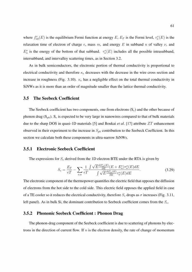
61
where f νn0(E) is the equilibrium Fermi function at energy E, EF is the Fermi level, τ ν
n (E) is the
relaxation time of electron of charge e, mass m, and energy E in subband n of valley ν, and
Eνn is the energy of the bottom of that subband. τ ν
n (E) includes all the possible intrasubband,
intersubband, and intervalley scattering times, as in Section 3.2.
As in bulk semiconductors, the electronic portion of thermal conductivity is proportional to
electrical conductivity and therefore κe decreases with the decrease in the wire cross section and
increase in roughness (Fig. 3.10). κe has a negligible effect on the total thermal conductivity in
SiNWs as it is more than an order of magnitude smaller than the lattice thermal conductivity.
3.5 The Seebeck Coefficient
The Seebeck coefficient has two components, one from electrons (Se) and the other because of
phonon drag (Sph). Se is expected to be very large in nanowires compared to that of bulk materials
due to the sharp DOS in quasi-1D materials [5] and Boukai et al. [17] attribute ZT enhancement
observed in their experiment to the increase in Sph contribution to the Seebeck Coefficient. In this
section we calculate both these components in ultra-narrow SiNWs.
3.5.1 Electronic Seebeck Coefficient
The expressions for Se derived from the 1D electron BTE under the RTA is given by
Se =EF
eT−
∑ν,n
1
eT
∫ √E
∂fνn0(E)
∂E(E + Eν
n)τ νn (E)dE∫ √
E∂fν
n0(E)
∂Eτ νn (E)dE
. (3.29)
The electronic component of the thermopower quantifies the electric field that opposes the diffusion
of electrons from the hot side to the cold side. This electric field opposes the applied field in case
of a TE cooler so it reduces the electrical conductivity, therefore Se drops as σ increases (Fig. 3.11,
left panel). As in bulk Si, the dominant contribution to Seebeck coefficient comes from the Se.
3.5.2 Phononic Seebeck Coefficient : Phonon Drag
The phonon-drag component of the Seebeck coefficient is due to scattering of phonons by elec-
trons in the direction of current flow. If n is the electron density, the rate of change of momentum
62
3 4 5 6 7 8200
220
240
260
280
300
320
340
Wire thickness and width [nm]
Se [µ
VK
−1 ]
∆ = 0.1 nm∆ = 0.2 nm∆ = 0.3 nm∆ = 0.4 nm
3 4 5 6 7 8
2
4
6
8
10
12
14
Wire thickness and width [nm]
Sph
[µV
K−
1 ]
∆ = 0.125 nm∆ = 0.25 nmRTA diffuse
Figure 3.11 Electronic (left) and phonon-drag (right) components of the Seebeck coefficient as a
function of the SiNW cross section and rms of surface roughness. The electronic component of
the Seebeck coefficient is more than an order of magnitude greater than the phonon-drag
component. Phonon drag component decreases with increasing roughness at the interface,
because of the decrease in the mean free path of phonons.
per unit volume due to a uniform electric field F is −neF. This momentum can be passed on to
impurities or defects, get lost to random thermal vibrations, or can be passed on to phonons that
carry the heat. Let η be the fraction of electron-acoustic phonon scattering rate to the total electron
scattering rate, µ be the electron mobility, and τph be the momentum relaxation time of acoustic
phonons (due to phonon scattering with other phonons, electrons, impurities, and boundary). The
net excess momentum per unit volume (∆p) carried by acoustic phonons due to their interaction
with electrons and the current density J due to the applied field are given by
∆p = −ηneτphF,
J = neµF.(3.30)
If υph is the velocity of acoustic phonons, the rate of heat flow per unit cross sectional area that
corresponds to the momentum gained from the electrons is w = υ2ph∆p. This heat flow results in a
Peltier current, characterized by the Peltier coefficient
Πph =w
j= −ηυ2
phτph
µ. (3.31)
63
The Seebeck coefficient corresponding to this can be obtained by using the Kelvin relation Sph =
Πph/T . Thus the phonon-drag component of the Seebeck coefficient is given by
Sph = −ηυ2phτph
µT. (3.32)
The phonon-drag component of the Seebeck coefficient has the same sign as that of the electronic
component of the Seebeck efficient and therefore it results in an increased thermopower.
The variation of the phononic contribution to the Seebeck coefficient with the SiNW cross sec-
tion is highly non-trivial. With decreasing wire cross section, η and τph [see Eq. (3.32)] decrease
monotonically, because of the increase in the electron scattering from SRS, and the increase in
phonon-phonon and phonon-boundary scattering, respectively. The interplay of these two varia-
tions with the mobility variation (see Chapter 2, Sec. 2.2.6.3) determines the Sph variation shown
in the right panel of Fig. 3.11. Comparing the results for Se and Sph, we find that the phonon-drag
contribution to the thermopower is negligible compared to the electronic contribution. This con-
tradicts the results shown by Boukai et al. [17]. But, the total S = Se + Sph from their experiment
agrees well with the total Seebeck coefficient from our calculations.
The phonon drag component decreases with the increase in randomization of phonons. There-
fore phonon drag component decreases with an increase in the roughness of the surface. In fact,
for κl ∼ 1 Wm−1K−1, Sph is almost 2 orders of magnitude smaller than that in bulk silicon and
therefore becomes negligibly small. It should be noted that the above results imply that Sph cannot
increase when κl decreases (this is in direct contradiction to that reported by Boukai et al. [17]).
3.6 ZT Dependence on the Silicon Nanowire Cross Section
The flowchart of the electrothermal simulator developed to model the TE figure of merit of
SiNWs is shown in Fig. (3.12). Once electrical conductivity (σ), Seebeck Coefficient (S =
Se + Sph), and thermal conductivity (κ = κe + κl) are calculated, the TE figure of merit at room
temperature is calculated from ZT = S2σ/κT . Fig. 3.13 shows the ZT variation with the wire
cross section calculated by solving the electron and phonon BTE. ZT in SiNWs is larger than that
in bulk silicon; the enhancement comes primarily because of an order of magnitude decrease in

64
phS
Monte Carlo (MC)
Method
Poisson Solver
Schrödinger Solver
Surface Roughness
Acoustic Phonons
Intervalley Phonons
Impurity
SOR
ARPACK
Relaxation Time
Approximation
Solve Electron
BoltzmannTransport Equation
ee S,κ Electron Mobility σµ),(
Solve Elastic Continuum
Equation
Acoustic Phonon
Dispersion and Group Velocity
Solve Phonon
BoltzmannTransport Equation
Relaxation Time
Approximation
Boundary - Phonon
Normal,UmklappThree Phonon
Electron, Impurity
Phonon Relaxation Time phph κτ ),(
phS phS
Monte Carlo (MC)
Method
Poisson Solver
Schrödinger Solver
Surface Roughness
Acoustic Phonons
Intervalley Phonons
Impurity
SOR
ARPACK
Relaxation Time
Approximation
Solve Electron
BoltzmannTransport Equation
ee S,κ Electron Mobility σµ),(
Monte Carlo (MC)
Method
Poisson Solver
Schrödinger Solver
Poisson Solver
Schrödinger Solver
Surface Roughness
Acoustic Phonons
Intervalley Phonons
Impurity
Surface Roughness
Acoustic Phonons
Intervalley Phonons
Impurity
SOR
ARPACK
SOR
ARPACK
Relaxation Time
Approximation
Solve Electron
BoltzmannTransport Equation
ee S,κ ee S,κ Electron Mobility σµ),(Electron Mobility σµ),(
Solve Elastic Continuum
Equation
Acoustic Phonon
Dispersion and Group Velocity
Solve Phonon
BoltzmannTransport Equation
Relaxation Time
Approximation
Boundary - Phonon
Normal,UmklappThree Phonon
Electron, Impurity
Phonon Relaxation Time phph κτ ),(
Solve Elastic Continuum
Equation
Acoustic Phonon
Dispersion and Group Velocity
Solve Phonon
BoltzmannTransport Equation
Relaxation Time
Approximation
Boundary - Phonon
Normal,UmklappThree Phonon
Electron, Impurity
Boundary - Phonon
Normal,UmklappThree Phonon
Electron, Impurity
Phonon Relaxation Time phph κτ ),(
Figure 3.12 The flowchart of the electrothermal simulator used to calculate the ZT of SiNWs.
3 4 5 6 7 80
0.5
1
1.5
2
Wire thickness and width [nm]
The
rmoe
lect
ric fi
gure
of m
erit
ZT Hicks and Dresselhaus
RTA diffuse∆ = 0.25 nm
Figure 3.13 ZT variation with the nanowire cross section. In extremely thin wires, contrary to
conventional belief, decreasing the cross section does not result in an exponential increase in ZT
because of the rapid decrease in electrical conductivity owing to strong electron-surface
roughness scattering. ZT obtained assuming complete diffuse boundary scattering for phonons
(red) is definitely an overestimation. ZT obtained using the actual surface defined by rms = 0.25
nm in phonon Monte Carlo (blue). Prediction from Hicks and Dresselhauss [5], showing
exponential increase in ZT with decreasing wire cross section (black).
65
the lattice thermal conductivity due to strong phonon-boundary scattering and not due to an en-
hancement in the power factor. ZT does not increase exponentially with decreasing wire cross as
predicted by Hicks and Dresselhauss [5], because in ultra-narrow wires, roughening (apart from
degrading thermal conductivity) severely degrades electrical conductivity.
3.7 Conclusion
A detailed electrothermal simulator has been developed to solve the electron and phonon Boltz-
mann transport equations and is used to calculate the thermoelectric figure of merit in SiNWs. ZT
in rough SiNWs has been found to be 30 times higher than that in bulk silicon because of an order
of magnitude decrease in the lattice thermal conductivity.
• As in bulk semiconductors, the Seebeck coefficient in SiNWs is determined by electrons,
while phonons dominate thermal conduction.
• Both electrical and thermal conductivity decrease with decreasing wire cross section. Com-
pared to the bulk value, the decrease in thermal conductivity is several times larger than the
decrease in electrical conductivity.
• The mean free path of phonons in nanowires is more than an order of magnitude smaller
than that in bulk silicon: the phonon drag component of the Seebeck coefficient cannot be
large in nanowires because it is proportional to the mean free path of phonons.
• The ZT in SiNWs does not increase exponentially when the wire cross section decreases be-
cause of a significant reduction in electrical conductivity with decreasing wire cross section.
• It is extremely important to account for the actual surface defined by its rms roughness in
both electronic and thermal transport calculations in order to correctly estimate the ZT in
SiNWs.
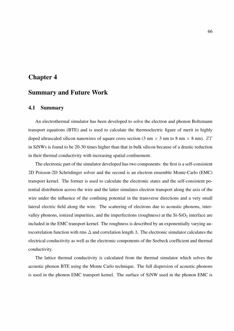
66
Chapter 4
Summary and Future Work
4.1 Summary
An electrothermal simulator has been developed to solve the electron and phonon Boltzmann
transport equations (BTE) and is used to calculate the thermoelectric figure of merit in highly
doped ultrascaled silicon nanowires of square cross section (3 nm × 3 nm to 8 nm × 8 nm). ZT
in SiNWs is found to be 20-30 times higher than that in bulk silicon because of a drastic reduction
in their thermal conductivity with increasing spatial confinement.
The electronic part of the simulator developed has two components: the first is a self-consistent
2D Poisson-2D Schrodinger solver and the second is an electron ensemble Monte-Carlo (EMC)
transport kernel. The former is used to calculate the electronic states and the self-consistent po-
tential distribution across the wire and the latter simulates electron transport along the axis of the
wire under the influence of the confining potential in the transverse directions and a very small
lateral electric field along the wire. The scattering of electrons due to acoustic phonons, inter-
valley phonons, ionized impurities, and the imperfections (roughness) at the Si-SiO2 interface are
included in the EMC transport kernel. The roughness is described by an exponentially varying au-
tocorrelation function with rms ∆ and correlation length Λ. The electronic simulator calculates the
electrical conductivity as well as the electronic components of the Seebeck coefficient and thermal
conductivity.
The lattice thermal conductivity is calculated from the thermal simulator which solves the
acoustic phonon BTE using the Monte Carlo technique. The full dispersion of acoustic phonons
is used in the phonon EMC transport kernel. The surface of SiNW used in the phonon EMC is
67
generated using a Fast Fourier Transform (FFT) technique from a given autocorrelation function.
Phonon scattering with impurites, other phonons (both normal and umklapp 3-phonon processes),
and the boundaries of the wire are included in the phonon EMC to describe the phonon transport in
SiNWs accurately. Apart from the lattice thermal conductivity, the thermal simulator is also used
to calculate the acoustic phonon mean free path, which is then used to calculate the phonon drag
component of the Seebeck coefficient.
The electrical conductivity decreases with deceasing wire cross section because of the strong
increase in the electron surface roughness scattering and phonon scattering. With increasing con-
finement, the energy separation between the conduction band edge (EC) and the Fermi level (EF )
increases, which results in an increase in the average energy carried by electrons, therefore the
Seebeck coefficient increases as the wire cross section decreases. The power factor does not show
an exponential increase with decreasing wire cross section as predicted in earlier theoretical stud-
ies because the electrical conductivity there is almost 6-fold decrease in σ and less than 2-fold
increase in the Seebeck coefficient when the wire cross section is decreased from 8 nm × 8 nm to
3 nm × 3 nm. The thermal conductivity decreases with decreasing wire cross section because of
the increase in phonon-boundary scattering. For the roughness parameters considered (∆ = 0.25
nm and Λ = 2.5 nm), the lattice thermal conductivity is about 25-75 times smaller (depending on
the wire cross section) than that of bulk silicon. The phonon drag component of the Seebeck coef-
ficient is negligibly small in SiNWs because of a strong reduction in the phonon mean free path.
Also, as in bulk silicon, the electronic contribution to thermal conductivity is more than an order
of magnitude smaller than the contribution from phonons.
The ZT in SiNWs calculated from the themoelectric simulator is about 30 times larger than
that in bulk silicon: the enhancement in ZT occurs primarily because of the decrease in the lattice
thermal conductivity due to strong phonon-boundary scattering and not due to an enhancement in
the power factor. ZT does not increase drastically with decreasing wire cross as predicted by ear-
lier studies, because in ultra-narrow wires, roughening (apart from degrading thermal conductivity)
severely degrades electrical conductivity. It is extremely important to account for the actual rough
surface when solving the electron and phonon BTE in order to estimate ZT in nanostructures.
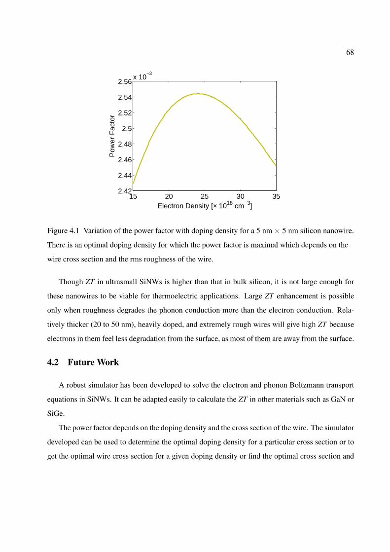
68
15 20 25 30 352.42
2.44
2.46
2.48
2.5
2.52
2.54
2.56x 10
−3
Electron Density [× 1018 cm−3]
Pow
er F
acto
r
Figure 4.1 Variation of the power factor with doping density for a 5 nm × 5 nm silicon nanowire.
There is an optimal doping density for which the power factor is maximal which depends on the
wire cross section and the rms roughness of the wire.
Though ZT in ultrasmall SiNWs is higher than that in bulk silicon, it is not large enough for
these nanowires to be viable for thermoelectric applications. Large ZT enhancement is possible
only when roughness degrades the phonon conduction more than the electron conduction. Rela-
tively thicker (20 to 50 nm), heavily doped, and extremely rough wires will give high ZT because
electrons in them feel less degradation from the surface, as most of them are away from the surface.
4.2 Future Work
A robust simulator has been developed to solve the electron and phonon Boltzmann transport
equations in SiNWs. It can be adapted easily to calculate the ZT in other materials such as GaN or
SiGe.
The power factor depends on the doping density and the cross section of the wire. The simulator
developed can be used to determine the optimal doping density for a particular cross section or to
get the optimal wire cross section for a given doping density or find the optimal cross section and
69
doping density that would give the maximum power factor. The variation of power factor for a 5
nm × 5 nm wire is shown in Fig. (4.1). We see that the power factor is maximal for a doping of
about 2.4 × 1019 cm−3. Note that σ varies with rms roughness, therefore the optimal density for a
different roughness will be different. The roughness in this case is ∆ = 0.25 nm.
4.2.1 Lattice Thermal Conductivity Modeling
In the phonon Monte Carlo, the phonons are reflected when they encounter the Si/SiO2 inter-
face. Although this is justified because of the mismatch in the acoustic impedance between silicon
and the oxide, few phonons can travel into the oxide. This effect can be included in the simula-
tion by calculating the transmission probability from the acoustic mismatch model or the diffuse
mismatch model [132].
In a recent study of thermal conductivity in ultrathin silicon membranes, Aksamija and Kneze-
vic [133] have shown that anisotropy in the phonon dispersion can play a significant role in deter-
mining the phonon-boundary scattering. In the current work, the dispersion for phonons is assumed
to be isotropic; anisotropic dispersion can be included in the future extension of this work.
In order to accurately compute lattice thermal conductivity in quasi-1D semiconductors, such
as SiNWs, a new theoretical model needs to be developed. This involves the following:
• Derive the expression for the scattering rate of phonons with other phonons, electrons, im-
purities, and rough boundaries, by properly accounting for 2D confinement of both phonons
and electrons in NWs. As phonon-boundary scattering plays a dominant role in determin-
ing κl in SiNWs, a sophisticated model similar to the Ando’s model for electron-surface
roughness scattering has to be developed.
• Use the full set of dispersion and the expression derived from the 1D phonon BTE to calcu-
late the κl.
• Investigate the phonon-drag component of the Seebeck coefficient in more detail. Guenault
[134] has suggested a current balance model for calculating Sph. This model is similar to
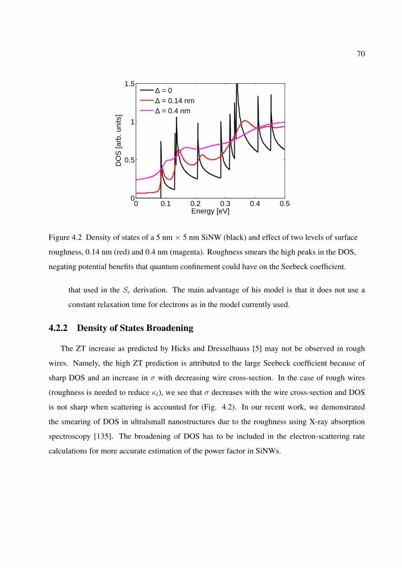
70
0 0.1 0.2 0.3 0.4 0.50
0.5
1
1.5
Energy [eV]
DO
S [a
rb. u
nits
]
∆ = 0∆ = 0.14 nm∆ = 0.4 nm
Figure 4.2 Density of states of a 5 nm × 5 nm SiNW (black) and effect of two levels of surface
roughness, 0.14 nm (red) and 0.4 nm (magenta). Roughness smears the high peaks in the DOS,
negating potential benefits that quantum confinement could have on the Seebeck coefficient.
that used in the Se derivation. The main advantage of his model is that it does not use a
constant relaxation time for electrons as in the model currently used.
4.2.2 Density of States Broadening
The ZT increase as predicted by Hicks and Dresselhauss [5] may not be observed in rough
wires. Namely, the high ZT prediction is attributed to the large Seebeck coefficient because of
sharp DOS and an increase in σ with decreasing wire cross-section. In the case of rough wires
(roughness is needed to reduce κl), we see that σ decreases with the wire cross-section and DOS
is not sharp when scattering is accounted for (Fig. 4.2). In our recent work, we demonstrated
the smearing of DOS in ultralsmall nanostructures due to the roughness using X-ray absorption
spectroscopy [135]. The broadening of DOS has to be included in the electron-scattering rate
calculations for more accurate estimation of the power factor in SiNWs.

71
LIST OF REFERENCES
[1] A. Majumdar, Science 303, 777 (2004).
[2] N. Nishiguchi, Physica E 13(1), 1 (2002).
[3] N. Nishiguchi, Y. Ando, and M. N. Wybourne, J. Phys.: Condens. Matter 9, 5751 (1997).
[4] P. Martin, Z. Aksamija, E. Pop, and U. Ravaioli, Phys. Rev. Lett. 102, 125503 (2009).
[5] L. D. Hicks and M. Dresselhaus, Phys. Rev. B 47, 16631 (1993).
[6] E. Pop, R. Dutton, and K. Goodson, J. Appl. Phys. 96, 4998 (2004).
[7] R. J. Dossat, Principles of refrigeration (Wiley, New York, 1978).
[8] M. Labudovic and J. Li, IEEE Trans. Compon. Packag. Tech. 27, 724 (2004).
[9] F. J. DiSalvo, Science 285, 703 (1999).
[10] H. J. Goldsmid, Thermoelectric Refrigeration (Plenum, New York, 1964).
[11] E. Altenkirch, Physikalische Zeitschrift 12, 920 (1911).
[12] X. Lu and J. Chu, J. Appl. Phys. 100(1), 014305 (2006).
[13] H. J. Goldsmid and R. Douglas, Br. J. Appl. Phys. 5, 386 (1954).
[14] L. D. Hicks and M. Dresselhaus, Phys. Rev. B 47, 12727 (1993).
[15] R. Venkatasubramanian, E. Siivola, T. Colpitts, and B. O’Quinn, Nature 413, 597 (2001).
[16] A. I. Hochbaum, R. Chen, R. Delgado, W. Liang, E. Garnett, M. Najarian, A. Majumdar,and P. Yang, Nature 451, 163 (2008).
[17] A. I.Boukai, Y. Bunimovich, J. Tahir-Kheli, J. Yu, W. A. G. III, and J. R. Heath, Nature 451,168 (2008).
[18] G. Nolas, J. Sharp, and J. Goldsmid, Thermoelectrics: Basic Principles and New MaterialsDevelopments (Springer, New York, 2001).
72
[19] G. A. Slack, CRC Handbook of Thermoelectrics (CRC Press, Boca Raton, FL, 1995), pp.407–440.
[20] R. Chen, A. H. P. Murphy, J. Moore, P. Yang, , and A. Majumdar, Phys. Rev. Lett. 101,105501 (2008).
[21] J. Zou and A. Balandin, J. Appl. Phys. 89(5), 2932 (2001).
[22] D. Li, Y. Wu, P. Kim, L. Shi, P. Yang, and A. Majumdar, Appl. Phys. Lett. 83, 2934 (2003).
[23] D. Lacroix, K. Joulain, D. Terris, and D. Lemonnier, Appl. Phys. Lett. 89(10), 103104(2006).
[24] N. Mingo, L. Yang, D. Li, and A. Majumdar, Nano. Lett. 3, 1713 (2003).
[25] E. B. Ramayya, D. Vasileska, S. M. Goodnick, and I. Knezevic, J. Appl. Phys. 104(6), 1(2008).
[26] S. Jin, M. V. Fischetti, and T. Tang, J. Appl. Phys. 102(8), 083715 (2007).
[27] A. Balandin and K. L. Wang, Phys. Rev. B 58(3), 1544 (1998).
[28] E. B. Ramayya, D. Vasileska, S. M. Goodnick, and I. Knezevic, J. Comput. Electron. 7, 319(2008).
[29] E. B. Ramayya, D. Vasileska, S. M. Goodnick, and I. Knezevic, presented at the NPMS-7/SIMD-5 (2005).
[30] E. B. Ramayya, D. Vasileska, S. M. Goodnick, and I. Knezevic, presented at the NSTINanotechnology Conference and Trade Show (2006).
[31] E. B. Ramayya, D. Vasileska, S. M. Goodnick, and I. Knezevic, presented at the IEEESilicon Nanoelectronics Workshop (2006).
[32] E. B. Ramayya, D. Vasileska, S. M. Goodnick, and I. Knezevic, presented at the IEEEConference on Nanotechnology (2006).
[33] E. B. Ramayya, D. Vasileska, S. M. Goodnick, and I. Knezevic, IEEE Trans. Nanotechnol.6(1), 113 (2007).
[34] I. Knezevic, E. B. Ramayya, D. Vasileska, and S. M. Goodnick, J. Comput. Theor. Nanos.6, 1725 (2009).
[35] E. Ramayya and I. Knezevic, J. Comput. Electron. 9, 206 (2010).
[36] E. B. Ramayya, D. Vasileska, S. M. Goodnick, and I. Knezevic, presented at the Meeting ofthe Electrochemical Society (2007).
73
[37] E. B. Ramayya, D. Vasileska, S. M. Goodnick, and I. Knezevic, presented at the Interna-tional Workshop on Computational Electronics (2007).
[38] E. B. Ramayya, D. Vasileska, S. M. Goodnick, and I. Knezevic, presented at the Interna-tional Conference on Nanoscience + Technology (2008).
[39] E. B. Ramayya, D. Vasileska, S. M. Goodnick, and I. Knezevic, presented at the IEEEConference on Nanotechnology (2008).
[40] E. B. Ramayya and I. Knezevic, Conference on the Physics and Chemistry of Surfaces andInterfaces (2009).
[41] E. B. Ramayya and I. Knezevic, March Meeting of the American Physical Society (2009).
[42] E. B. Ramayya and I. Knezevic, International Workshop on Computational Electronics(2009).
[43] E. B. Ramayya and I. Knezevic, March Meeting of the American Physical Society (2010).
[44] Z. Aksamija, E. B. Ramayya, and I. Knezevic, IEEE Silicon Nanoelectronics Workshop(2010).
[45] E. B. Ramayya and I. Knezevic, International Workshop on Computational Electronics(2010).
[46] E. B. Ramayya and I. Knezevic, Sumitted (2010).
[47] H. Sakaki, Jpn. J. Appl. Phys. 19(12), L735 (1980).
[48] V. Arora, Phys. Stat. Sol. (b) 105, 707 (1981).
[49] J. Lee and H. Spector, J. Appl. Phys. 54(7), 3921 (1983).
[50] J. Lee and M. Vassell, J. Phys. C: Solid State Phys. 17, 2525 (1984).
[51] G. Sanders, C. Stanton, and Y. Yang, Phys. Rev. B 48(15), 11067 (1993).
[52] J. Wang, A. Rahman, A. Ghosh, G. Klimeck, and M. Lundstrom, IEEE Trans. ElectronDevices 52(7), 1589 (2005).
[53] Y. Zheng, C. Rivas, R. Lake, K. Alam, T. B. Boykin, and G. Klimeck, IEEE Trans. ElectronDevices 52(6), 1097 (2005).
[54] C. Harris and E. O’Reilly, Physica E 32, 341 (2006).
[55] M. Nolan, S.O’Callaghan, G. Fagas, and J. Greer, Nano Lett. 7(1), 34 (2007).
[56] K. Nehari, N. Cavassilas, and F.Michelini, Appl. Phys. Lett. 90(13), 132112 (2007).

74
[57] E. Gnani, S. Reggiani, A. Gnudi, P. Parruccini, R. Colle, M. Rudan, and G. Baccarani, IEEETrans. Electron Devices 54(9), 2243 (2007).
[58] A. Buin, A. Verma, A. Svizhenko, and M. Anantram, Nano Lett. 8(2), 760 (2008).
[59] B. Auld, Acoustic fields and waves in solids (Wiley-Interscience, New York, 1973).
[60] S. Yu, K. W. Kim, M. A. Stroscio, G. J. Iafrate, and A. Ballato, Phys. Rev. B 50(3), 1733(1994).
[61] S. Yu, K. W. Kim, M. A. Stroscio, and G. J. Iafrate, Phys. Rev. B 51(7), 4695 (1995).
[62] A. Svizhenko, S. Bandyopadhyay, and M. A. Stroscio, J. Phys.: Condens. Matter 10, 6091(1998).
[63] R. W. Morse, J. Acoust. Soc. Am. 22(2), 219 (1950).
[64] S.-M. Koo, A. Fujiwara, J.-P. Han, E. M. Vogel, C. A. Richter, and J. E. Bonevich, NanoLett. 4(11), 2197 (2004).
[65] R. Kotlyar, B. Obradovic, P. Matagne, M. Stettler, and M. D. Giles, Appl. Phys. Lett. 84(25),5270 (2004).
[66] J. Wang, E. Polizzi, A. Ghosh, S. Datta, and M. Lundstrom, Appl. Phys. Lett. 87, 043101(2005).
[67] M. Lenzi, P. Palestri, E. Gnani, S. Reggiani, A. Gnudi, D. Esseni, L. Selmi, and G. Bac-carani, IEEE Trans. Electron Devices 55(8), 2086 (2008).
[68] O. Gunawan, L. Sekaric, A. Majumdar, M. Rooks, J. Appenzeller, J. W. Sleight, S. Guha,and W. Haensch, Nano Lett. 8, 1566 (2008).
[69] M. Lundstrom and Z. Ren, IEEE Trans. Electron Devices 49(1), 133 (2002).
[70] M. Lundstrom, IEDM Tech. Dig. 33(1), 789 (2003).
[71] A. Godoy, F. Ruiz, C. Sampedro, F. Gamiz, and U. Ravaioli, Solid-State Electron. 51, 1211(2007).
[72] Y. Cui, Z. Zhong, D. Wang, W. U. Wang, and C. Lieber, Nano Lett. 3(2), 149 (2003).
[73] A. Sharma, S.H.Zaidi, S. Lucero, S. Brueck, and N. Islam, IEE Proc.-Circuits Devices Syst.5(151), 422 (2004).
[74] M. Dutta, M. A. Stroscio, and K. Kim, Int. J. High Speed Electronics and Systems 9(1), 281(1998).
[75] A. A. Balandin, J. Nanoscience and Nanotechnology 5(7), 1 (2005).

75
[76] E. P. Pokatilov, D. L. Nika, and A. A. Balandin, Superlattices and Microstructures 33(3),155 (2003).
[77] E. P. Pokatilov, D. L. Nika, and A. A. Balandin, Phys. Rev. B 72(11), 113311 (2005).
[78] X. Lu, J. H. Chu, and W. Z. Shen, J. Appl. Phys. 93(2), 1219 (2003).
[79] Y. Chen, D. Li, J. R. Lukes, and A. Majumdar, J. Heat Transfer 127(10), 1129 (2005).
[80] C. M. S. Torres, A. Zwick, F. Poinsotte, J. Groenen, M. Prunilla, J. Ahopelto, A. Mlayah,and V. Paillard, Phys. Status Solidi C 1(11), 2609 (2004).
[81] F. Gamiz, P. Cartujo-Cassinello, J. B. Roldan, C. Sampedro, and A. Godoy, SOI symposiumof the Electrochemical Society (2005).
[82] L. Donetti, F. Gamiz, J. B. Roldan, and A. Godoy, J. Appl. Phys. 100(1), 013701 (2006).
[83] L. Donetti, F. Gamiz, F. Jimenez, and C. Sampedro, Appl. Phys. Lett. 88(12), 122108(2006).
[84] W. M. Visscher, A. Migliori, T. M. Bell, and R. A. Reinert, J. Acoust. Soc. Am. 90(4)(1991).
[85] T. Ando, A. B. Fowler, and F. Stern, Rev. Mod. Phys. 54, 437 (1982).
[86] S. Takagi, J. Koga, and A. Toriumi, Jpn. J. Appl. Phys. 37(3B), 1289 (1998).
[87] F. Gamiz, Appl. Phys. Lett. 84(2), 299 (2004).
[88] K. Uchida, J. Koga, and S. Takagi, J. Appl. Phys. 102, 074510 (2007).
[89] F. Balestra, S. Cristoloveanu, M. Benachir, J. Brini, and T. E. Elewa, IEEE Electron Dev.Lett. 8(9), 410 (1987).
[90] H. Majima, H. Ishikuro, and T. Hiramoto, IEEE Electron Dev. Lett. 21(8), 396 (2000).
[91] http://www.caam.rice.edu/software/ARPACK/ (2002).
[92] C. Jacoboni and L. Reggiani, Rev. Mod. Phys. 55, 645 (1983).
[93] M. V. Fischetti and S. E. Laux, Phys. Rev. B 48(4), 2244 (1993).
[94] S. M. Goodnick, D. K. Ferry, C. W. Wilmsen, Z. Liliental, D. Fathy, and O. L. Krivanek,Phys. Rev. B 32(12), 8171 (1985).
[95] F. Gamiz and M. V. Fischetti, J. Appl. Phys. 89(10), 5478 (2001).
[96] E. P. Pokatilov, D. L. Nika, and A. A. Balandin, Superlattices and Microstructures 38(3),168 (2005).

76
[97] Y. S. Ju and K. E. Goodson, Appl. Phys. Lett. 74(20), 3005 (1999).
[98] W. Weber, Phys. Rev. B 15(10), 4789 (1977).
[99] S. P. Hepplestone and G. P. Srivastava, Phys. Status Solidi C 1(11), 2617 (2004).
[100] R. Shishir and D. K. Ferry, J. Comput. Electron. 7, 305 (2008).
[101] D. Hisamoto, W.-C. Lee, J. Kedzierski, H. Takeuchi, K. Asano, C. Kuo, E. Anderson, T.-J.King, J. Bokor, and C. Hu, IEEE Trans. Electron Devices 47(12), 2320 (2000).
[102] A. W. T. T. M. Vo, V. Lordi, and G. Galli, Nano Lett. 8(4), 1111 (2008).
[103] M. Lundstrom, Fundamentals of Carrier Transport (Addison-Wesley Publishing CompanyInc., New York, 1992).
[104] R. Sajjad, K. Alam, and Q. Khosru, Semicond. Sci. Technol. 24, 045023 (2009).
[105] H. Mera, M. Persson, Y. Niquet, and M. Bescond, International Workshop on ComputationalElectronics (2010).
[106] H. Kosina and G. Kaiblinger-Grujina, Solid-State Electron. 42(3), 331 (1998).
[107] J. Watling, L. Yang, M. Borici, R. Wilkins, A. Asenov, J. Barker, and S. Roy, Solid-StateElectron. 48(8), 1337 (2004).
[108] P. Lugli and D. Ferry, IEEE Trans. Electron Devices ED-32(11), 2431 (1985).
[109] A. Khitun, A. Balandin, and K. L. Wang, Superlattices and Microstructures 26(3), 181(1999).
[110] X. Lu, W. Z. Shen, and J. H. Chu, J. Appl. Phys. 91(3), 1542 (2002).
[111] P. Klemens, Solid state physics (Academic Press, NY, 1958).
[112] J. Callaway, Phys. Rev. 113, 1046 (1959).
[113] S. Mazumder and A. Majumdar, J. Heat Transfer 123(4), 749 (2001).
[114] D. Lacroix, K. Joulain, and D. Lemonnier, Phys. Rev. B 72(6), 064305 (2005).
[115] P. K. Schelling, S. S. Phillipot, and P. Keblinski, Phys. Rev. B 65, 144306 (2002).
[116] S. G. Volz and G. Chen, Phys. Rev. B 61, 2651 (2000).
[117] P. Chantrenne and J.-L. Barrat, J. Heat Transfer 126, 577 (2004).
[118] J. Tersoff, Phys. Rev. B 39, 5566 (1989).
77
[119] P. Heino, Eur. Phys. J. B 60, 171 (2007).
[120] I. Ponomareva, D. Srivastava, and M. Menon, Nano Lett. 7(5), 1155 (2007).
[121] N. Papanikolaou, J. Phys.: Condens. Matter 20, 135201 (2008).
[122] B. Becker, P. K. Schelling, and S. R. Phillipot, J. Appl. Phys. 99, 123715 (2006).
[123] A. J. Kulkarni and M. Zhou, Nanotechnology 18, 435706 (2007).
[124] Z. Wang, F. Gao, J.-P. Crocombette, X. T. Zu, L. Yang, and W. J. Weber, Phys. Rev. B 75,153303 (2007).
[125] J. Che, T. Cagin, W. Deng, and W. A. G. III, J. Chem. Phys. 113, 6888 (2000).
[126] M. Asheghi, K. Kurabayashi, R. Kasnavi, and K. Goodson, J. Appl. Phys. 91, 5079 (2002).
[127] R. Prasher, T. Tong, and A. Majumdar, Nano Lett. 8(1), 99 (2008).
[128] R. Peterson, J. Heat Transfer 116, 815 (1994).
[129] A. Mittal and S. Mazumder, J. Heat Transfer 132, 052402 (2010).
[130] S. M. Goodnick, D. K. Ferry, C. W. Wilmsen, Z. Liliental, D. Fathy, and L. Krivanek, Phys.Rev. B 32, 8171 (1985).
[131] J.-J. Wu, Tribology International 33, 47 (2000).
[132] T. Klitsner, J. VanCleve, H. Fischer, and R. Pohl, J. Heat Transfer 38, 7576 (1988).
[133] Z. Aksamija and I. Knezevic, Phys. Rev. B (82), 045319 (2010).
[134] A. Guenault, J. Phys. F: Metal Phys. 1, 373 (1971).
[135] F. Chen, E. Ramayya, C. Euaruksakul, F. Himpsel, G. Celler, B. Ding, I. Knezevic, andM. Lagally, ACS Nano. 4, 2466 (2010).
[136] X. Aymerich-Humet, F. Serra-Mestres, and J. Millan, Solid-State Electron. 24, 981 (1981).
[137] A. Abramo, A. Cardin, L. Selmi, and E. Sangiorgi, IEEE Trans. Electron Devices 47, 1858(2000).
[138] M. Modest, Radiative Heat Transfer (Acadmic Press, New York, 2003).
78
Appendix A: Calculation of Electron Scattering Rates
A.1 Phonon Scattering
A.1.1 Bulk Acoustic Phonon Scattering Rate
The electron wavefunction in subband n, taking into account confinement along the y and z
directions and free motion along x, is
Ψn(r) = ψn(y, z)eikxx. (A.1)
The displacement field u due to longitudinal phonons in the second-quantization form can be
written as
u(r) =∑
q
√h
2ρΩωq
(aqe
iqr + a†qe−iqr
)eq, (A.2)
where, aq and a†q are the phonon annihilation and creation operators respectively, Ω is the volume,
ρ is the density, and eq is the polarization vector.
The perturbing potential which goes into the matrix element calculation is given by
Hac = Ξac∇ · u, (A.3)
where Ξac is the acoustic deformation potential and u is the phonon displacement given by Eq.(A.2).
From Eqs. (A.2) and (A.3), we can write the perturbing potential as
Hac = Ξac
∑q
√h
2ρΩωqeq · iq
(aqe
iqr − a†qe−iqr
). (A.4)
The matrix element after integrating over phonon coordinates, for scattering from subband n with
wavevector kx to subband m with k′x is given by
79
Mnm(kx, k′x) = Ξac
√h
2ρΩωqq
(Nq +
1
2∓1
2
) 12
×∫∫ [
ψn(y, z)ei(qyy+qzz)ψm(y, z)]dy dz
× 1
Lx
∫e
i(kx−k
′x±qx
)xdx,
(A.5)
where Nq is the number of phonons given by the Bose-Einstein distribution function
Nq =1
ehωq
KBT − 1. (A.6)
Defining Inm (qy, qz) as
Inm (qy, qz) =
∫∫ [ψn(y, z)ei(qyy+qzz)ψm(y, z)
]dy dz (A.7)
and after integrating over x, Eq. (A.5) yields∣∣∣Mnm(kx, k′x)
∣∣∣2
= Ξ2ac
h
2ρΩωqq2
(Nq +
1
2∓1
2
)
× |Inm (qy, qz)|2 δ(kx − k′x±qx).
(A.8)
In the equipartition approximation, the phonon number becomes
Nq≈Nq + 1≈KBT
hωq, (A.9)
so using the equipartition approximation and linear dispersion relation for acoustic phonons de-
fined by ωq = υsq in Eq. (A.8), we get
∣∣∣Mnm(kx, k′x)∣∣∣2
= 2Ξ2ac
hq2
2ρΩυsq
KBT
hυsq
× |Inm (qy, qz)|2 δ(kx − k′x + qx),
(A.10)
where υs is the sound velocity in the crystal.
Acoustic phonon scattering rate using Fermi’s Golden Rule with the elastic scattering approx-
imation is given by
Γacnm(kx) =
2π
h
∑
q‖,k′x
∣∣∣Mnm(kx, k′x)∣∣∣2
δ(E − E ′), (A.11)
80
where E and E ′ are the initial and final energies of the scattered electron in the parabolic band
approximation, respectively.
Substituting Eq. (A.10) in Eq. (A.11) and changing the sum to an integral, we get
Γacnm(kx) =
2πΩΞ2acKBT
ρΩυ2s h
∫∫|Inm (qy, qz)|2dqydqz
4π2
×∫
δ(kx − k
′x + qx
)δ(E − E ′) dk
′x
2π.
(A.12)
To evaluate Eq. (A.12), let us rewrite it as
Γacnm(kx) =
2πΞac2KBT
hρυ2s
DnmI2, (A.13)
where
I2 =1
2π
∫δ(kx − k
′x + qx)δ(E − E ′) dkx
′, (A.14)
Dnm =1
4π2
∫∫|Inm (qy, qz)|2dqydqz. (A.15)
The above equation can be written as
Dnm =1
4π2
∫dqy
∫dqz
×∫∫ [
ψn(y, z)ei(qyy+qzz)ψm(y, z)]dy dz
×∫∫ [
ψn(y′, z
′)e−i
(qyy
′+qzz
′)ψm(y
′, z
′)
]dy
′dz
′.
(A.16)
Using the identity1
2π
∫dqye
iqy(y−y′) = δ(y − y
′), (A.17)
we can write (A.16) as
Dnm =
∫∫|ψn(y, z)|2|ψm(y, z)|2 dy dz . (A.18)
Adding a nonparabolicity factor α and converting the dk′x integration to dE ′ integration, the
integral in Eq. (A.14) simplifies to
I2 =1
2π
√m∗
2h2
1 + 2αEf√Ef (1 + αEf ), (A.19)
81
where Ef is the final kinetic energy of the electron after scattering. It is defined in terms of initial
parabolic kinetic energy Ekx as
Ef = En − Em +
√1 + 4αEkx − 1
2α. (A.20)
Substituting the above simplified integrals in Eq. (A.13) we get
Γacnm(kx) =
Ξac2KBT
√2m∗
h2ρυ2s
Dnm1 + 2αEf√Ef (1 + αEf )
Θ(Ef ). (A.21)
where Θ(Ef ) is the Heaviside step function that ensures a positive kinetic energy after scattering.
A.1.2 Intervalley Scattering Rate
Intervalley scattering can be mediated by long-wavevector acoustic phonons or non-polar opti-
cal phonons. Intervalley scattering is modeled using the non-polar optical phonon model.
The perturbing potential which goes into the matrix element calculation is given by
Hiv(q) = Ξiveq · u, (A.22)
where Ξiv is the intervalley deformation potential and u is the phonon displacement given by Eq.
(A.2).
Assuming intervalley phonons to be dispersionless, i.e., ωq = ω0, Eq. (A.22) can be written as
Hiv = Ξiv
∑q
√h
2ρΩω0
(aqe
iqr + a†qe−iqr
). (A.23)
The matrix element for intervalley scattering is given by
Mnm(kx, k′x) =Ξiv
√h
2ρΩω0
(Nq +
1
2∓1
2
) 12
× Inm (qy, qz) δ(kx − k′x±qx),
(A.24)
where the emission and absorption of an optical phonon results in (Nq + 1)12 and (Nq)
12 , respec-
tively, and Inm (qy, qz) is the overlap integral defined in Eq. (A.7).

82
Following the procedure outlined above to calculate acoustic phonon scattering rate and ac-
counting for the inelastic nature of scattering due to optical phonons, we can write the optical
phonon scattering rate as
Γivnm(kx) =
πΞ2iv
ρω0
(Nq +
1
2∓1
2
)
×∫∫
|Inm (qy, qz)|2dqydqz
4π2
×∫
δ(kx − k
′x±qx
)δ(E − E ′±hω0)
dk′x
2π,
(A.25)
where δ(E − E ′±hω0) ensures the conservation of energy after absorption (top sign) and emission
(bottom sign) of a phonon of energy hω0. Simplifying this using the approach followed in the
previous section (A.1.1), intervalley phonon scattering rate can be written as
Γivnm (kx) =
Ξ2iv
√m∗
√2hρω0
(Nq +
1
2∓ 1
2
)Dnm
× (1 + 2αEf )√Ef (1 + αEf )Θ(Ef ),
(A.26)
where the final kinetic energy Ef is similar to that in Eq. (A.20), with ±hω0 to account for absorp-
tion (top sign) and emission (bottom sign) of a phonon.
A.1.3 Confined Acoustic Phonon Scattering Rate
Using the xyz algorithm, the normalized displacement components for the J th acoustic phonon
mode in terms of a complete set of basis functions Φλ can be written as
uJ,i = αJχJ,iλΦλ, (A.27)
where i = (x, y, z) represents one of the components of the displacement, αJ is the normalization
constant and χJ,iλ are the coefficients of the basis functions.
Taking the center of cross section of the wire as the origin, the basis functions in terms of
powers of Cartesian coordinates in the lateral directions are
83
Φλ(x, y, z) =
(2z
W
)r (2y
H
)s
eiqxx, (A.28)
where λ = (r, s), qx is the longitudinal wavevector of the acoustic phonon mode along the axis of
the wire, and W and H are the width and thickness of the wire, respectively.
Following the normalization procedure indicated in Ref. [3], we get the normalization constant
in Eq. (A.27) to be
αJ =1√
WHLx
√h
2ωJ
1√χ†
JEχJ
, (A.29)
where Lx is the length of the wire, ωJ is the frequency of the J th phonon mode, and χJ is the
eigenvector corresponding to ωJ . E is the matrix as defined in Ref. [3].
The acoustic phonon field, which is used to determine the perturbing potential, is given by
u =∑J,qx
[aJqxuJqx + a†Jqxu∗Jqx
]eq.
Considering Eq. (A.30) instead of Eq. (A.2) to represent the phonon displacement, the matrix
element given by Eq. (A.5) can be rewritten as
Mnm(kx, k′x) =ΞacαJ
(NJqx +
1
2∓1
2
) 12
Lnm(J, qx)
× 1
Lx
∫e
i(kx−k
′x±qx
)xdx,
(A.30)
where NJqx = [exp(hωJ(qx)/kBT )− 1]−1 is the number of acoustic phonons of energy hωJ(qx)
and Lnm(J, qx) is the electron-phonon overlap integral given by
Lnm(J, qx) =
∫∫ [ψn(y, z)
2rχJ,1λ
W
(2z
W
)r−1 (2y
H
)s
+2sχJ,2λ
H
(2z
W
)r (2y
H
)s−1
+ iqxχJ,3λ
(2z
W
)r (2y
H
)s
ψm(y, z)
]dy dz.
(A.31)
84
The square of the matrix element is then given by∣∣∣Mnm(kx, k
′x)
∣∣∣2
= Ξ2ac
(NJqx +
1
2∓1
2
)|αJ |2
× |Lnm(J, qx)|2 δ(kx − k′x±qx).
(A.32)
Considering the confined acoustic phonon scattering to be inelastic, the scattering rate can now
be written as
Γacnm (kx) =
2πΞ2ac
h
∑J,qx
(NJqx +
1
2∓1
2
)|αJ |2
× |Lnm(J, qx)|2 δ(kx − k′x±qx)δ(E − E
′±hωJ(qx)),
(A.33)
where the upper and lower signs denote absorption and emission of an acoustic phonon of energy
hωJ(qx), respectively. Integrating over qx and including the non-parabolicity factor, the scattering
rate can be written as
Γacnm(kx) =
Ξ2ac
2WH
∑J
∫dqx
(NJqx +
1
2∓1
2
)|Lnm(J, qx)|2
× 1
ωJ(qx)∣∣∣χ†
JqxEχJqx
∣∣∣δ(E − E
′±hωJ(qx)),
where the total energy of the electron before (E) and after (E ′) scattering are defined as
E = En +
√1 + 4α h2k2
x
2m− 1
2α,
E′= Em +
√1 + 4α h2(kx±qx)2
2m− 1
2α,
(A.34)
The argument of the delta function in Eq. (A.34) can have two roots. Using the identity for delta
functions with multiple roots, the final expression for the scattering rate is
Γacnm(kx) =
Ξ2ac
2WH
∑J
∑i=1,2
(NJqxi
+1
2±1
2
)
× 1
ωJ(qxi)∣∣∣χ†
JqxiEχJqxi
∣∣∣|Lnm(J, qxi
)|2|g′(qxi
)| ,
85
where g(qx) = (E−E′∓hωJ(qx)), qx1 and qx2 are the two possible roots of g(qx) = 0, and g
′(qx1)
and g′(qx2) are the derivatives of g(qx) with respect qx evaluated at qx1 and qx2, respectively.
A.2 Surface Roughness Scattering
In a very simple model used to describe the surface roughness scattering, the perturbing poten-
tial for the interface normal to the y direction is given by
Hsr = eεy(y, z)4(x), (A.35)
where 4(x) is a random function which describes the deviation of the actual interface from the
ideal flat interface and εy(y, z) is the field normal to the interface. The scattering matrix calculated
using this perturbing potential is
Mnm(kx, k′x) =e
∫∫[ψn(y, z)εy(y, z)ψm(y, z)] dy dz
× 1
Lx
∫4(x)ei(kx−k
′x)x dx.
(A.36)
Defining the term in the double integral of the above equation as Fnm, the square of the matrix
element can be written as
∣∣∣Mnm(kx, k′x)∣∣∣2
=e2F2nm
1
L2x
∫dx
′
×∫
dx4(x)4(x′)ei(x−x
′)·(kx−k
′x).
(A.37)
The average value of the matrix element given by Eq. (A.37) over many samples is actually used
to calculate the SRS. The expectation value of the square of the matrix element is given by
⟨∣∣∣Mnm(kx, k′x)∣∣∣2⟩
=e2F2nm
1
L2x
∫dx
′
×∫
dx〈4(x)4(x′)〉ei(x−x
′)·qx ,
(A.38)
where the correlation function R(x − x′) = 〈4(x)4(x
′)〉 depends only on the distance |x − x
′|,and qx = (kx − k
′x). Redefining (x− x
′) as x” we get
86
⟨∣∣∣Mnm(kx, k′x)∣∣∣2⟩
= e2F2nm
1
L2x
∫dx
′∫
dx”R(x”)eix”qx . (A.39)
Assuming exponentially correlated surface roughness [94] defined by R(x) = ∆2e−√
2|x|λ in Eq.
(A.39), we get
⟨∣∣∣Mnm(kx, k′x)∣∣∣2⟩
= e2F2nm
1
L2x
∆2Lx2√
2λ
(q±x )2λ2 + 2. (A.40)
The scattering rate due to the interface imperfections can now be written as
Γsrnm(kx) =
2π
h
∑
k′x
e2F2nm
1
Lx
∆2 2√
2λ
q2xλ
2 + 2δ(E ′ − E). (A.41)
Converting the sum over k′x to integral over dk
′x, we get
Γsrnm(kx) =
2π
he2F2
nm
2√
2λ∆2
Lx
×Lx
2π
∫dk
′x
1
(kx±k′x)2λ2 + 2
δ(E ′ − E).
(A.42)
Defining Ei =√
1+4αEkx−12α
and redefining (q±x )2 as 2m/h2(√Ei(1 + αEi) ±
√Ef (1 + αEf ))2,
the final expression for surface roughness scattering assuming non parabolic bands can be written
as
Γsrnm(kx,±) =
2√
m∗e2
h2
∆2Λ
2 + (q±x )2Λ2|Fnm|2
× (1 + 2αEf )√Ef (1 + αEf )Θ(Ef ).
(A.43)
Unlike the approach detailed above, Ando’s model [85] of interface roughness scattering ac-
counts for deformation of both the wavefunction and potential due to the imperfection at the Si-
SiO2 interfaces. The matrix element including the perturbation to wavefunction and the potential
87
using Ando’s model is given by
Mnm(kx, k′x) =
∫∫dydz
∫dx
e−ik′xx
√L
ψm(y +4(x), z)
×[H0 +4V (y +4(x), z)
]ψn(y +4(x), z)
− ψm(y, z)H0ψn(y, z)
eikxx
√L
,
(A.44)
where the unperturbed system is represented by the Hamiltonian H0 and wavefunctions ψn(y, z)
and ψm(y, z), and the perturbed system’s Hamiltonian and wavefunction are[H0 + 4V (y +
4(x), z)]
and ψm(y + 4(x), z) and ψn(y + 4(x), z). Calculating the scattering rate from this
matrix element, we find that the final expression for the SRS is same as before except that, we have
additional wavefunction deformation terms in the SRS overlap integral Fnm. The SRS overlap
integral is given in Eq. (2.6).
A.3 Impurity Scattering
Coulomb potential due to an ionized impurity of charge Ze, located at R(y0, z0) from the center
of the wire cross section, felt by an electron at position (r(y, z), x) is given by
U(r, x) = − Ze2
4πεsi
√(r− R)2 + x2
e−√
(r−R)2+x2
Ld , (A.45)
where εsi is the dielectric constant of silicon and Łd is the degenerate Thomas-Fermi screening
length [106, 107]. The matrix element for the impurity-electron scattering can be written as
Mnm(kx, k′x) =− Ze2
4πεsi
∫∫ψn(y, z)
1
Lx
∫ei(kx−k
′x)xe
−√
(r−R)2+x2
Ld√(r− R)2 + x2
dx
ψm(y, z)dy dz.
(A.46)
Defining q = |kx − k′x|,
K0(q, R) =
∫eiqxe
−√
(r−R)2+x2
Ld√(r− R)2 + x2
dx, (A.47)
88
Inm(q, R) =
∫∫ψn(y, z)K0(q, R)ψm(y, z)dy dz, (A.48)
and E and E ′ as the initial and final energies of the scattered electron in the parabolic band approx-
imation, the scattering rate from a single impurity using Fermi’s Golden Rule is
Γinm(kx) =
2π
h
Z2e4
16π2ε2siL
2x
∑
k′x
I2nm(q, R)δ(E − E ′). (A.49)
The total impurity-electron scattering rate due to an uniform doping density of Na is obtained by
integrating over the position R of the dopants
Γimpnm (kx) =
Z2e4
16π2hε2siLx
∫dR NaLx
∫dk
′x I2nm(q, R)δ(E − E ′). (A.50)
Adding a nonparabolicity factor α and converting the dk′x integration to dE
′ integration, the Eq.
(A.50) becomes
Γimpnm (kx) =
Z2e4Na
√m
16√
2π2h2ε2si
(1 + 2αEf )√Ef (1 + αEf )
∫dR I2nm(q±x , R). (A.51)
where Ef is the final kinetic energy defined in Eq. (A.20) and q±x = kx ± k′x is the difference
between the initial and final electron wavevectors as defined in the SRS derivation.

89
Appendix B: Self-consistent Poisson-Schrodinger-Monte CarloSolver
The simulator developed to calculate the electron mobility has two components: the first is
a self-consistent 2D Poisson-2D Schrodinger solver and the second is a Monte-Carlo transport
kernel. The former is used to calculate the electronic states and the self-consistent potential distri-
bution along the cross section of the wire and the latter simulates the transport along the wire axis.
For the SiNWs considered, the confinement is along the y and z directions and the electrons are
allowed to move freely in the x direction.
B.0.1 Self-consistent 2D Poisson–2D Schrodinger solver
The Hamiltonian for an electron, residing in one of the six valleys (ν) is of the form
H0(r) = −(
h2
2mνx
∂2
∂x2+
h2
2mνy
∂2
∂y2+
h2
2mνz
∂2
∂z2
)+ V (y, z)
= H0||(x) + H0⊥(y, z), (B.1)
where r = (x, y, z), V (y, z) is the potential energy profile of the confining potential in the (y, z)-
plane (obtained from the Hartree potential, the solution to the 2D Poisson’s equation), H0|| is the
parallel part of H0 (associated with the motion along the axis of the wire), and the transverse part
is defined as
H0⊥(y, z) = − h2
2mνy
∂2
∂y2− h2
2mνz
∂2
∂z2+ V (y, z). (B.2)
The basis-states of the unperturbed Hamiltonian are assumed to be of the form
ψν,n(r) =1√L
eikxxψν,n(y, z), (B.3)
where kx is the wavevector along the axis of the wire of length L and the wavefunction ψν,n(y, z)
of subband with energy Eν,n satisfies the 2D Schrodinger equation
H0⊥(y, z)ψν,n(y, z) = Eν,nψν,n(y, z). (B.4)
Because of the pronounced mass anisotropy in the Si material system and the multi-valley
nature of the lowest conduction bands, the six conduction band valleys are included through a
90
standard three-valley-pair model. Valley pair 1 along the (100) direction have masses mx = ml
and my = mz = mt, valley pair 2 along the (010) direction have masses mx = mz = mt and
my = ml, and valley pair 3 along the (001) direction have masses mx = my = mt and mz = ml.
An accurate description of the charge and potential in a nanowire requires a self-consistent
solution of the 2D Schrodinger equation [Eq. (B.4)] and the 2D Poisson equation
∂
∂y
[ε(y, z)
∂ϕ(y, z)
∂y
]+
∂
∂z
[ε(y, z)
∂ϕ(y, z)
∂z
]= −e
[N+
D −N−A + p(y, z)− n(y, z)
], (B.5)
where ϕ(y, z) is the electrostatic Hartree potential and V (y, z) = −eϕ(y, z), ε(y, z) is the spatially-
dependent dielectric constant, N+D and N−
A are the ionized donor and acceptor concentrations,
and n(y, z) and p(y, z) are the electron and hole densities, respectively. The electron density is
calculated using
n(y, z) = 2∑ν,n
Nν,n |ψν,j(y, z)|2 , (B.6)
where the factor 2 accounts for the valley degeneracy and Nν,n is the electron line density in the
n-th subband of the ν-th valley pair, given by
Nν,n =1
πh
√2mν
xkBT F−1/2
(EF − Eν,n
kBT
), (B.7)
where EF is the Fermi energy, kB is the Boltzmann constant, and T is the temperature. The
Fermi-Dirac integral of order −1/2 can be approximated as [136, 137]
F−1/2(η) =
∫ ∞
0
u−1/2du
1 + eu−η'
√π
e−η +√
π2
1√η+b+[a+(|η−b|)c]1/c
, (B.8)
where η = (EF −Eν,n)/kBT , a = 6.68, b = 1.72, and c = 4.11. These equations can be solved by
using finite difference discretization scheme described in Ref. [34]. The steps involved in solving
these two equations self-consistently is described below.
Step 1 Initialization: Poisson’s equation is solved in the entire 2D cross-section, whereas the
Schrodinger equation needs to be solved only in the silicon region and a small region of oxide
near the Si-SiO2 interface. As most of the interesting physics happens near the interfaces, a fine
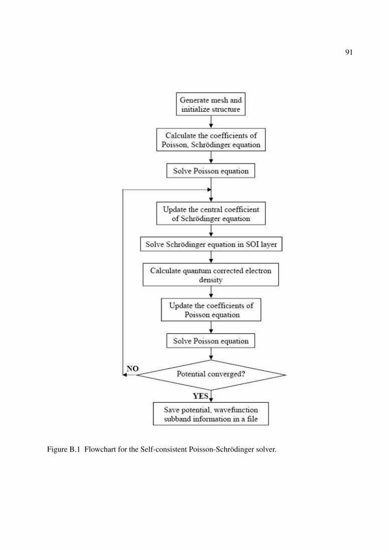
91
Figure B.1 Flowchart for the Self-consistent Poisson-Schrodinger solver.
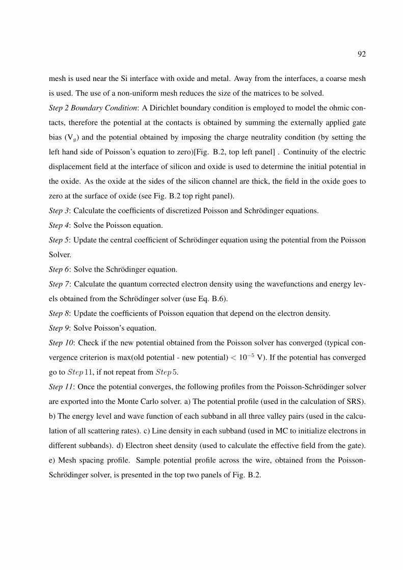
92
mesh is used near the Si interface with oxide and metal. Away from the interfaces, a coarse mesh
is used. The use of a non-uniform mesh reduces the size of the matrices to be solved.
Step 2 Boundary Condition: A Dirichlet boundary condition is employed to model the ohmic con-
tacts, therefore the potential at the contacts is obtained by summing the externally applied gate
bias (Vg) and the potential obtained by imposing the charge neutrality condition (by setting the
left hand side of Poisson’s equation to zero)[Fig. B.2, top left panel] . Continuity of the electric
displacement field at the interface of silicon and oxide is used to determine the initial potential in
the oxide. As the oxide at the sides of the silicon channel are thick, the field in the oxide goes to
zero at the surface of oxide (see Fig. B.2 top right panel).
Step 3: Calculate the coefficients of discretized Poisson and Schrodinger equations.
Step 4: Solve the Poisson equation.
Step 5: Update the central coefficient of Schrodinger equation using the potential from the Poisson
Solver.
Step 6: Solve the Schrodinger equation.
Step 7: Calculate the quantum corrected electron density using the wavefunctions and energy lev-
els obtained from the Schrodinger solver (use Eq. B.6).
Step 8: Update the coefficients of Poisson equation that depend on the electron density.
Step 9: Solve Poisson’s equation.
Step 10: Check if the new potential obtained from the Poisson solver has converged (typical con-
vergence criterion is max(old potential - new potential) < 10−5 V). If the potential has converged
go to Step 11, if not repeat from Step 5.
Step 11: Once the potential converges, the following profiles from the Poisson-Schrodinger solver
are exported into the Monte Carlo solver. a) The potential profile (used in the calculation of SRS).
b) The energy level and wave function of each subband in all three valley pairs (used in the calcu-
lation of all scattering rates). c) Line density in each subband (used in MC to initialize electrons in
different subbands). d) Electron sheet density (used to calculate the effective field from the gate).
e) Mesh spacing profile. Sample potential profile across the wire, obtained from the Poisson-
Schrodinger solver, is presented in the top two panels of Fig. B.2.
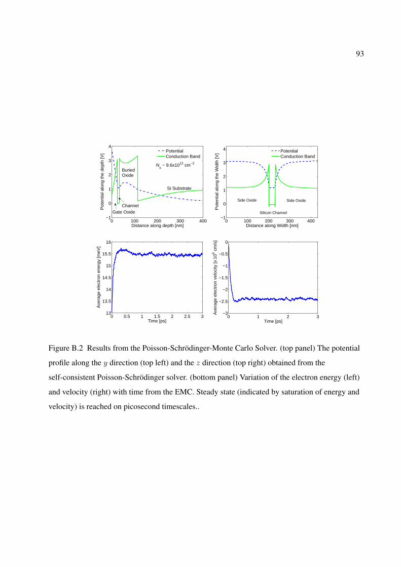
93
0 100 200 300 400−1
0
1
2
3
4
Distance along depth [nm]
Pot
entia
l alo
ng th
e de
pth
[V]
Ns ~ 9.6x1012 cm−2
PotentialConduction Band
Si Substrate
BuriedOxide
ChannelGate Oxide
0 100 200 300 400−1
0
1
2
3
4
Distance along Width [nm]
Pot
entia
l alo
ng th
e W
idth
[V] Potential
Conduction Band
Side Oxide Side Oxide
Silicon Channel
16
0 0.5 1 1.5 2 2.5 313
13.5
14
14.5
15
15.5
Time [ps]
Ave
rage
ele
ctro
n en
ergy
[meV
]
0
Ave
rage
ele
ctro
n ve
loci
ty [x
106 c
m/s
]
−0.5
−1
−1.5
−2
−2.5
0−3
1 2 3Time [ps]
Figure B.2 Results from the Poisson-Schrodinger-Monte Carlo Solver. (top panel) The potential
profile along the y direction (top left) and the z direction (top right) obtained from the
self-consistent Poisson-Schrodinger solver. (bottom panel) Variation of the electron energy (left)
and velocity (right) with time from the EMC. Steady state (indicated by saturation of energy and
velocity) is reached on picosecond timescales..

94
B.1 Semiclassical Transport Description
Electron transport in modern semiconductor devices can be described by the Boltzmann trans-
port equation (BTE), which is given in its common form as [103]
∂f
∂t+ v · ∇rf +
dpdt· ∇pf =
∑
k′S(k′, k)f(k′) [1− f(k)]− S(k, k′)f(k) [1− f(k′)] . (B.9)
The function f(r, p, t) (p = hk) is the electron distribution function, which gives the probability of
finding electrons at time t, located at position r, with momentum p. (Note all vectors in this section
are three-dimensional.) The second term (the diffusion term) on the left-hand side (LHS) of Eq.
(B.9) describes the net in-flow of electrons to an elementary volume centered at r in position space.
The third term (the drift term) on the LHS describes the net in-flow of electrons to an elementary
volume centered at p in momentum space, and is caused by external electric field. The right-hand
side (RHS) of Eq. (B.9) is the collision integral, representing the result of competition between
in-scattering and out-scattering. S(k, k′) is the transition rate from an initial state | k〉 to a final
state | k′〉, and can be calculated from the Fermi’s Golden Rule [103] as
S(k, k′) =2π
h|〈k′ | Hint | k〉|2 δ(E(k′)− E(k)∓ hω), (B.10)
where Hint is the interaction Hamiltonian and the δ-function reflects the conservation of energy.
Solution of the BTE provides the distribution function f(r, p, t) from which the macroscopic quan-
tities of interest (e.g., electron density, current density) are readily evaluated.
The BTE is a semiclassical transport description, since the LHS of the equation treats electrons
as classical particles, but the RHS treats electrons quantum mechanically (as waves). The semiclas-
sical transport description has two underlying assumptions: (i) the spatial variation of any external
potential is much greater than the de Broglie wavelength at which the wavelike nature of electrons
may be witnessed; (ii) the time of concern is much larger than the time between collisions that is
in the range of subpicoseconds. For the two assumptions to hold, dimensions of semiconductor
devices have to be relatively large and the time of concern needs to be relatively long. In addi-
tion, collisions are assumed to be mutually independent and instantaneously change the electron
momentum. Any applied electric field is treated as slowly varying, and it does not interfere with
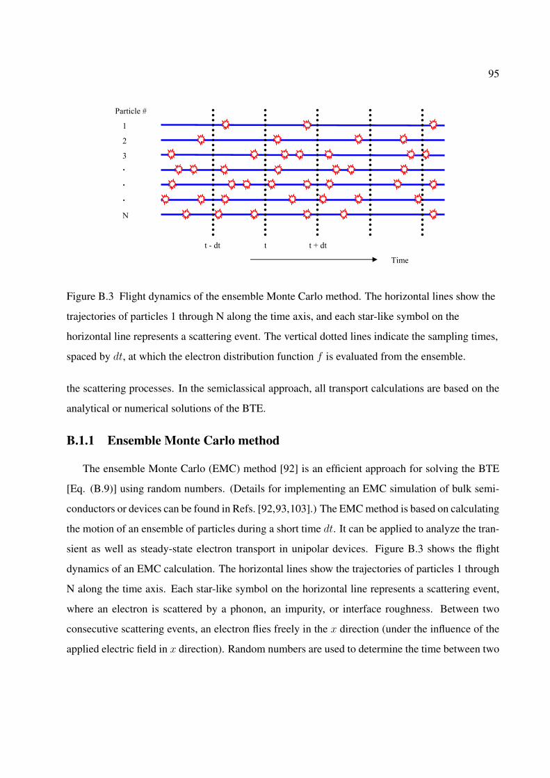
95
Time
t - dt t + dt t
1
2
N
3
.
.
.
Particle #
Figure B.3 Flight dynamics of the ensemble Monte Carlo method. The horizontal lines show the
trajectories of particles 1 through N along the time axis, and each star-like symbol on the
horizontal line represents a scattering event. The vertical dotted lines indicate the sampling times,
spaced by dt, at which the electron distribution function f is evaluated from the ensemble.
the scattering processes. In the semiclassical approach, all transport calculations are based on the
analytical or numerical solutions of the BTE.
B.1.1 Ensemble Monte Carlo method
The ensemble Monte Carlo (EMC) method [92] is an efficient approach for solving the BTE
[Eq. (B.9)] using random numbers. (Details for implementing an EMC simulation of bulk semi-
conductors or devices can be found in Refs. [92,93,103].) The EMC method is based on calculating
the motion of an ensemble of particles during a short time dt. It can be applied to analyze the tran-
sient as well as steady-state electron transport in unipolar devices. Figure B.3 shows the flight
dynamics of an EMC calculation. The horizontal lines show the trajectories of particles 1 through
N along the time axis. Each star-like symbol on the horizontal line represents a scattering event,
where an electron is scattered by a phonon, an impurity, or interface roughness. Between two
consecutive scattering events, an electron flies freely in the x direction (under the influence of the
applied electric field in x direction). Random numbers are used to determine the time between two

96
consecutive scattering events (also called the free-flight time), and to choose the proper scattering
process among many scattering mechanisms. The vertical dotted lines indicate the sampling times,
spaced by dt, at which the electron distribution function f is evaluated from the ensemble. Macro-
scopic quantities of interest (e.g., electron density, current density) can be readily evaluated from
the distribution f . The time interval dt should be chosen small enough (typically 1 femtosecond)
to capture the right electron dynamics.
Figure B.4 shows a flow chart of the ensemble Monte Carlo transport kernel used to solve
the BTE. Between scattering events, particles fly freely along the wire axis and remain in a given
subband. Input of the Monte Carlo transport kernel is provided by a self-consistent Schrodinger-
Poisson solver. Since the electrons in a wire are confined in two transverse directions, they are only
scattered in either the forward or the backward direction; consequently, just the carrier momentum
along the length of the wire needs to be updated after each scattering event. Upon reaching steady-
state (indicated by saturation of the average electron energy and drift velocity, see bottom panel of
Fig.B.2), mobility is calculated from the ensemble average of the electron velocities [92].
97
Start
Calculate scattering rates and
scattering table
t = 0
Initialize carriers i = 1
τ = freeflight(i)
Choose scattering mechanism
and select final state
New free flight time τ1
i = i+1
freeflight(i) = τ-dt
freeflight(i) = τ1-(τ-dt)
t = t+dt
Stop
τ > dt ?
N
τ1 > dt-τ ? Y
N
Y
t < total time ?
N
Y
i < Nmax ? Y
N
Final state empty ?
Update carrier state
Y
N
Figure B.4 Flowchart of the ensemble Monte Carlo transport kernel.
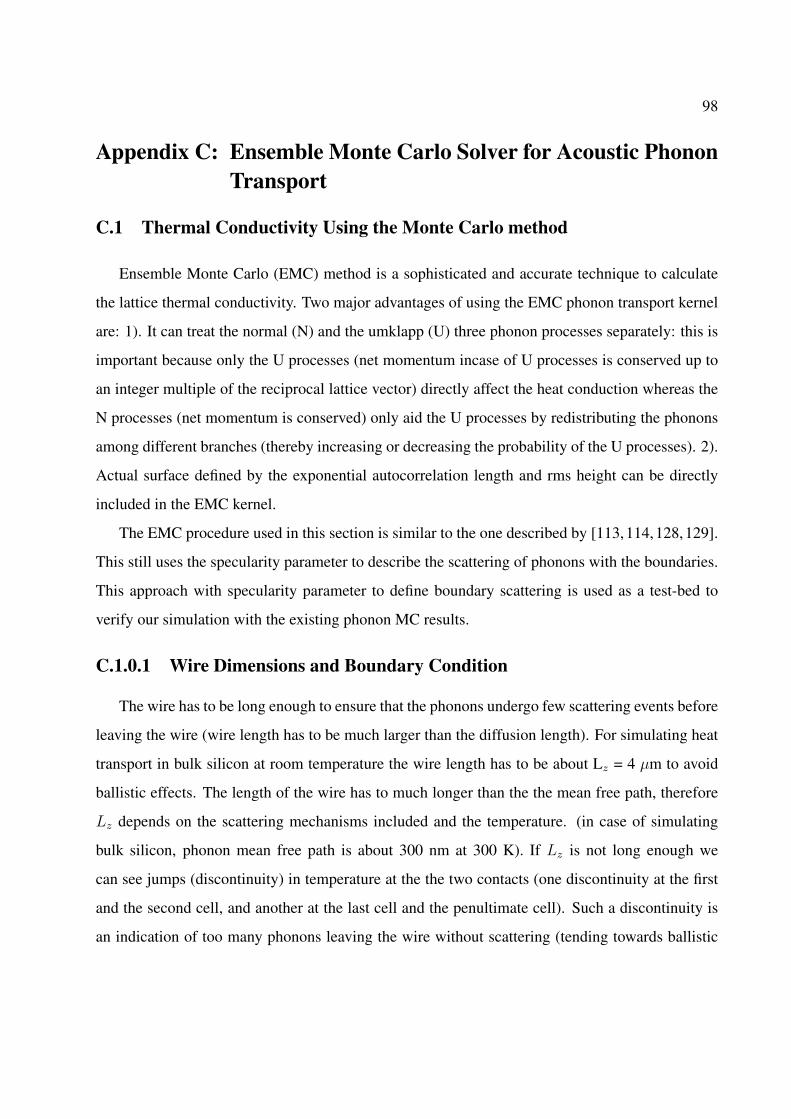
98
Appendix C: Ensemble Monte Carlo Solver for Acoustic PhononTransport
C.1 Thermal Conductivity Using the Monte Carlo method
Ensemble Monte Carlo (EMC) method is a sophisticated and accurate technique to calculate
the lattice thermal conductivity. Two major advantages of using the EMC phonon transport kernel
are: 1). It can treat the normal (N) and the umklapp (U) three phonon processes separately: this is
important because only the U processes (net momentum incase of U processes is conserved up to
an integer multiple of the reciprocal lattice vector) directly affect the heat conduction whereas the
N processes (net momentum is conserved) only aid the U processes by redistributing the phonons
among different branches (thereby increasing or decreasing the probability of the U processes). 2).
Actual surface defined by the exponential autocorrelation length and rms height can be directly
included in the EMC kernel.
The EMC procedure used in this section is similar to the one described by [113,114,128,129].
This still uses the specularity parameter to describe the scattering of phonons with the boundaries.
This approach with specularity parameter to define boundary scattering is used as a test-bed to
verify our simulation with the existing phonon MC results.
C.1.0.1 Wire Dimensions and Boundary Condition
The wire has to be long enough to ensure that the phonons undergo few scattering events before
leaving the wire (wire length has to be much larger than the diffusion length). For simulating heat
transport in bulk silicon at room temperature the wire length has to be about Lz = 4 µm to avoid
ballistic effects. The length of the wire has to much longer than the the mean free path, therefore
Lz depends on the scattering mechanisms included and the temperature. (in case of simulating
bulk silicon, phonon mean free path is about 300 nm at 300 K). If Lz is not long enough we
can see jumps (discontinuity) in temperature at the the two contacts (one discontinuity at the first
and the second cell, and another at the last cell and the penultimate cell). Such a discontinuity is
an indication of too many phonons leaving the wire without scattering (tending towards ballistic

99
Figure C.1 (top) Normal three-phonon scattering: two phonons with wavevectors K1 and K2
interact to give the third phonon of wavevector K3 and vice versa. In this case the net momentum
of the phonon system is unaltered. Although this type of scattering does not pose any resistance to
the heat flow directly, it can not be ignored, because it changes the distribution of phonons
thereby increasing or decreasing the umklapp three phonon scattering. (bottom) Umklapp
three-phonon scattering: two phonons with wavevectors K1 and K2 interact to give the third
phonon of wavevector K3. In this case the momentum is conserved up to an integer multiple of
the inverse lattice vector G. This directly poses resistance to heat flow because it can
reverse/change the direction of the heat flow.
100
transport). In order to estimate the thermal conductivity using the Fourier’s law, the transport has
to be diffusive and therefore the wire has to be long enough (so that phonons injected from the first
cell undergo enough scattering before leaving the wire). Note, for simulating phonon transport at
lower temperatures (sub 100 K) with just phonon-phonon scattering, the length of the wire has to
be more than 40 µm because the mean free path for phonons is few microns at low temperatures.
The width and thickness are assumed to be Lx = Ly = 500 nm so that the boundary scattering
with phonons is very week [114]. The axis of the wire is along the z direction and the four surfaces
of the wire are in the x and y directions. The wire is split into nz = 20 cells of dimensions 200
× 500 × 500 nm3. The boundaries along the two lateral directions are assumed to be perfectly
reflecting (in this case there is no boundary resistance, as the momentum of the phonon along
the axis of the wire is unaltered when it hits a boundary) or diffuse (the phonon directions is
randomized isotropically when it encounters a surface). The first and the last cells are treated as
black bodies and their temperatures are maintained throughout the simulation at the temperatures
to which they are initialized in the beginning (they are re-initialized at each time step to have the
same temperature). They act as the two thermal contacts. The phonons in the end cells travel with
their equilibrium velocities without undergoing any type of scattering. The phonons entering the
wire’s intermediate cells from these end cells correspond to the emission from the black bodies
and will automatically have the required distribution. When the phonons from the end cells leave
the wire, (i.e. when they hit the wall at z = 0 or z = Lz) they are deleted from the simulation.
When a phonon from an intermediate cell impinges on an end cell it is absorbed (i.e. it is deleted
from the simulation domain).
C.1.0.2 Number of Phonons and Dispersion
The first step in the initialization is to calculate the number of phonons that are to be used in
the simulation. The number of phonons N and their total energy E in a volume V at temperature
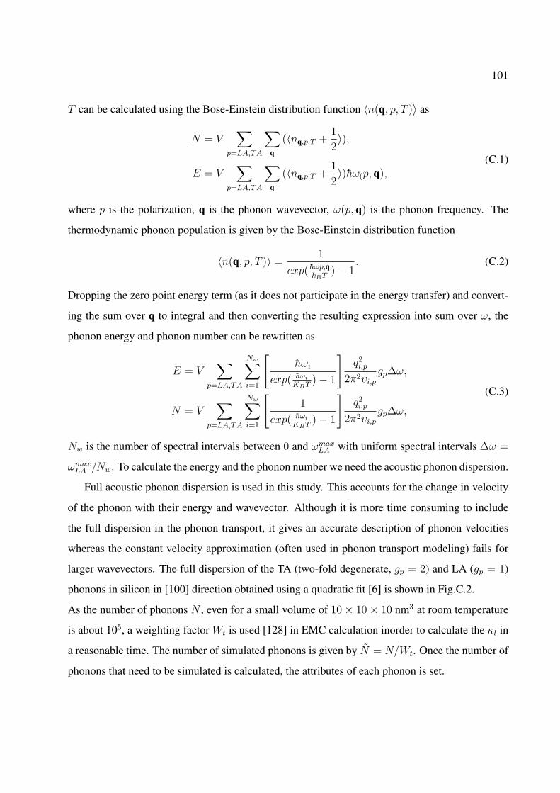
101
T can be calculated using the Bose-Einstein distribution function 〈n(q, p, T )〉 as
N = V∑
p=LA,TA
∑q
(〈nq,p,T +1
2〉),
E = V∑
p=LA,TA
∑q
(〈nq,p,T +1
2〉)hω(p, q),
(C.1)
where p is the polarization, q is the phonon wavevector, ω(p, q) is the phonon frequency. The
thermodynamic phonon population is given by the Bose-Einstein distribution function
〈n(q, p, T )〉 =1
exp( hωp,qkBT
)− 1. (C.2)
Dropping the zero point energy term (as it does not participate in the energy transfer) and convert-
ing the sum over q to integral and then converting the resulting expression into sum over ω, the
phonon energy and phonon number can be rewritten as
E = V∑
p=LA,TA
Nw∑i=1
[hωi
exp( hωi
KBT)− 1
]q2i,p
2π2υi,p
gp∆ω,
N = V∑
p=LA,TA
Nw∑i=1
[1
exp( hωi
KBT)− 1
]q2i,p
2π2υi,p
gp∆ω,
(C.3)
Nw is the number of spectral intervals between 0 and ωmaxLA with uniform spectral intervals ∆ω =
ωmaxLA /Nw. To calculate the energy and the phonon number we need the acoustic phonon dispersion.
Full acoustic phonon dispersion is used in this study. This accounts for the change in velocity
of the phonon with their energy and wavevector. Although it is more time consuming to include
the full dispersion in the phonon transport, it gives an accurate description of phonon velocities
whereas the constant velocity approximation (often used in phonon transport modeling) fails for
larger wavevectors. The full dispersion of the TA (two-fold degenerate, gp = 2) and LA (gp = 1)
phonons in silicon in [100] direction obtained using a quadratic fit [6] is shown in Fig.C.2.
As the number of phonons N , even for a small volume of 10 × 10 × 10 nm3 at room temperature
is about 105, a weighting factor Wt is used [128] in EMC calculation inorder to calculate the κl in
a reasonable time. The number of simulated phonons is given by N = N/Wt. Once the number of
phonons that need to be simulated is calculated, the attributes of each phonon is set.
102
0 2 4 6 8 100
1
2
3
4
5
6
7
Wavevector [× 109 m−1]
Pho
non
Fre
quen
cy [×
1013
rad
s−
1 ]
LA branchTA branch
Figure C.2 Acoustic phonon dispersion for LA and TA phonons in silicon in the fist Brillouin
zone obtained using a quadratic fit of the experimental data [6].
C.1.0.3 Phonon Attributes
The initial temperature of the first and the last cells are set to the hot (TH) and the cold (TL)
temperatures, respectively. All the intermediate cells are initialized to the lower temperature TL.
Given the temperature and the volume of each cell, the number of phonons that are to be simulated
in each cell N is calculated and their attributes such as the frequency, wavevector, velocity, and
polarization are determined from the phonon distribution and dispersion.
Frequency of the phonon (ω) is found from the normalized cumulative number density function
which is constructed from the number of phonons Ni in ith spectral interval and the total number
of phonons
Fi =i∑
k=1
Nk/
Nw∑
k=1
Nk. (C.4)
A random number R is selected, if Fi−1 ≤ R ≤ Fi then the phonon frequency is selected from
the ith spectral interval, ω = ω0,i + (2R − 1)∆ω2
, where ω0,i is the cental frequency of ith spectral
interval.
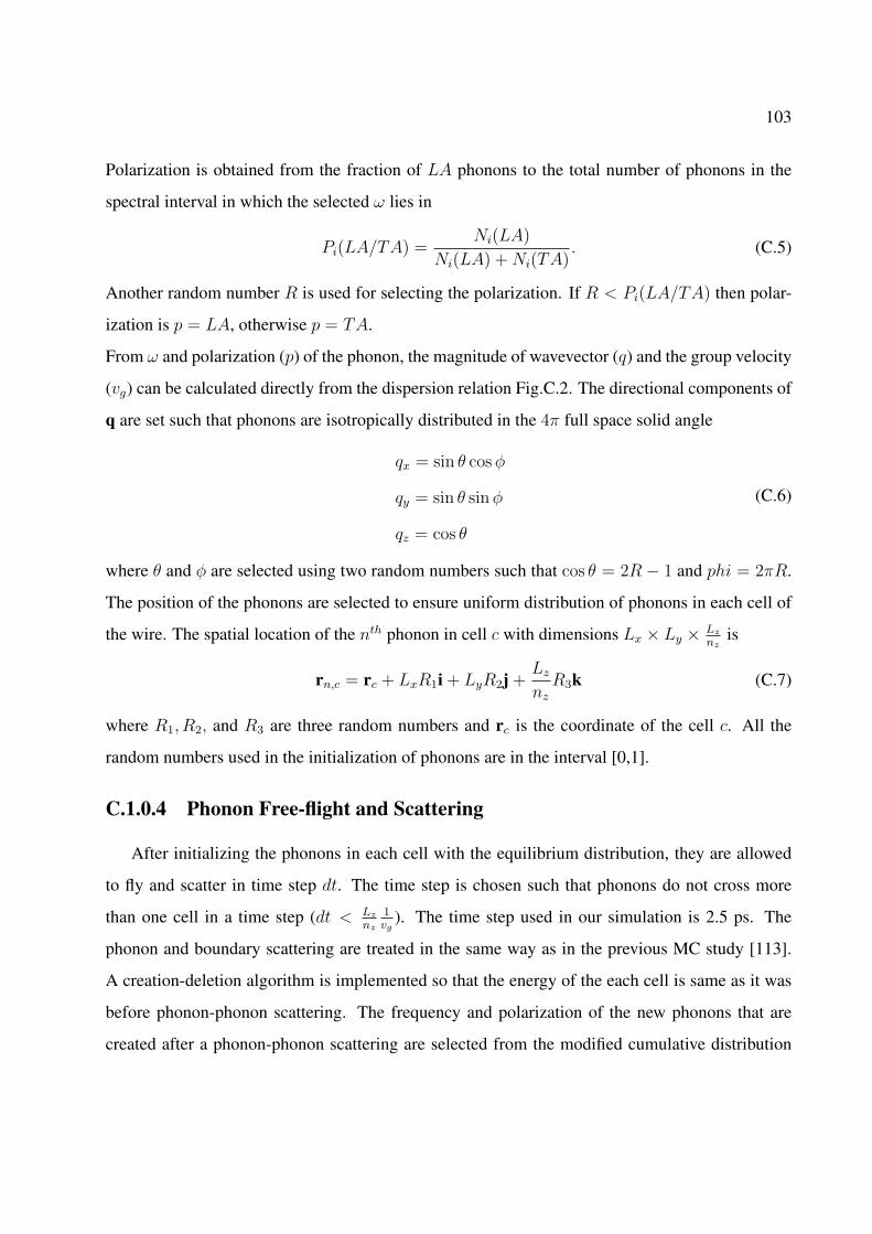
103
Polarization is obtained from the fraction of LA phonons to the total number of phonons in the
spectral interval in which the selected ω lies in
Pi(LA/TA) =Ni(LA)
Ni(LA) + Ni(TA). (C.5)
Another random number R is used for selecting the polarization. If R < Pi(LA/TA) then polar-
ization is p = LA, otherwise p = TA.
From ω and polarization (p) of the phonon, the magnitude of wavevector (q) and the group velocity
(vg) can be calculated directly from the dispersion relation Fig.C.2. The directional components of
q are set such that phonons are isotropically distributed in the 4π full space solid angle
qx = sin θ cos φ
qy = sin θ sin φ
qz = cos θ
(C.6)
where θ and φ are selected using two random numbers such that cos θ = 2R − 1 and phi = 2πR.
The position of the phonons are selected to ensure uniform distribution of phonons in each cell of
the wire. The spatial location of the nth phonon in cell c with dimensions Lx × Ly × Lz
nzis
rn,c = rc + LxR1i + LyR2j +Lz
nz
R3k (C.7)
where R1, R2, and R3 are three random numbers and rc is the coordinate of the cell c. All the
random numbers used in the initialization of phonons are in the interval [0,1].
C.1.0.4 Phonon Free-flight and Scattering
After initializing the phonons in each cell with the equilibrium distribution, they are allowed
to fly and scatter in time step dt. The time step is chosen such that phonons do not cross more
than one cell in a time step (dt < Lz
nz
1vg
). The time step used in our simulation is 2.5 ps. The
phonon and boundary scattering are treated in the same way as in the previous MC study [113].
A creation-deletion algorithm is implemented so that the energy of the each cell is same as it was
before phonon-phonon scattering. The frequency and polarization of the new phonons that are
created after a phonon-phonon scattering are selected from the modified cumulative distribution

104
5 10 15 20290
295
300
305
310
Cell Number
Tem
pera
ture
[K]
1 ps2 ns10 ns50 ns
Figure C.3 Transient temperature profile along the length of the wire for diffuse phonon
transport.In diffuse transport, a linear temperature profile is established along the length of the
wire when the system reaches steady state. The time taken to reach a steady state increases with
the increase in the length of the wire.
1 5 10 15 20290
295
300
305
310
Cell Number
Cel
l Tem
pera
ture
[K]
0 5000 10000 150005550
5600
5650
5700
5750
5800
5850
5900
Time step [normalized]
Tot
al e
nerg
y [n
orm
aliz
ed]
Figure C.4 The steady state temperature profile along the wire (left panel). Only phonon-phonon
scattering is considered. In the case of diffuse scattering, the steady state profile is linear along
the wire. The transient energy of all the phonons in the wire (right panel). The energy of the
system increases with time and saturates as the system reaches the steady state indicated by a
linear temperature profile.
105
1 5 10 15 2074
76
78
80
82
84
86
Cell Number
Cel
l Tem
pera
ture
[K]
0 2000 4000 6000 80001.15
1.2
1.25
1.3
1.35x 10
4
Time Step [normalized]
Tot
al e
nerg
y [n
orm
aliz
ed]
Figure C.5 The steady state temperature profile along the wire (left panel). Only phonon-phonon
scattering is considered. In the case of diffuse scattering, the steady state profile is linear along
the wire. In this case TH = 85 K and TL = 75 K. The mean free path of phonons in this case is few
microns, therefore, we can see discontinuity in temperature at the two end cells and linear profile
inside the wire signifying quasi-ballistic phonon transport. The transient energy of all the
phonons in the wire (right panel). The energy of the system increases with time and saturates as
the system reaches the steady state indicated by a linear temperature profile along the wire.

106
function F scati and P scat
i (LA/TA), respectively. This accounts for the change in the distribution of
phonons due to scattering. At the end of the time step dt, the total energy (ET ) of phonons in each
cell is calculated. The new temperature of each cell after dt is calculated from ET using numerical
inversion of energy relation to temperature
ET
VWt =
∑p=LA,TA
Nw∑i=1
hωi
exp( hωi
KBT)− 1
q2i,p
2π2υi,p
gp∆ω. (C.8)
Here Wt accounts for the fact that each phonon simulated is Wt physical phonons. The end cells
are re-initialized to their equilibrium distribution after each dt.
Since the second cell is at a lower temperature than the first cell, the heat flux entering it
will be higher than the outgoing flux. This will result in an increase in its temperature. As the
time progresses, the temperature in subsequent cells will also increase. In steady state, a linear
temperature profile will be established along the wire axis. Upon reaching steady state, Fourier’s
law is used to calculate κl from the net heat flux (Φ) crossing the interface between two adjoining
cells. To increase the accuracy, κl is calculated from Φ averaged over few thousand time steps.
The flux is given by
Φ =Wt
dt
Nc∑i=1
hωqz
|q| , (C.9)
where Nc is the number of phonons crossing the interface between two adjoining cells. The factorqz
|q| accounts for the normal component of the flux and the direction of the flux. The weighting
factor Wt, has to be included as each phonon in the simulation domain is actually Wt physical
phonons.
One way to check if the code is working or not is to see if the energy of the system is increasing
with time or not. Since, all the cells in the wire are initialized to a lower temperature than the
first cell temperature (contact cell), the first cell will inject more and more phonons into the wire
until steady state is reached: i.e. the energy of the system will increase until it reaches the steady
state. The steady state temperature profile for diffusive transport will be linear along the wire. The
transient temperature profile is shown in Fig. C.3 The temperature profile along the wire in steady
state and the variation of energy of the system with time are shown in Fig.(C.4).
107
The steady state temperature profile for a quasi-ballistic case is shown in Fig.(C.5). This can be
observed when the mean free path of phonons is comparable to the wire length. Since there is
scattering (although weak), a linear temperature is expected inside the wire with discontinuity at
the two contacts (because of too many injected phonons leaving the wire before undergoing any
scattering).
C.1.0.5 Diffuse Phonon-boundary Scattering
In the results shown so far, only phonon-phonon scattering is included. This was done to
verify our code with the results reported by Lacroix et al. in Ref. [114]. The code works as
expected with just phonon-phonon scattering. Then we added the boundary-phonon scattering in
the simulation. The boundary scattering is isotropic, therefore when a phonon is incident on the
surface, it is absorbed and a new phonon is emitted from that location. The emitted phonon’s
direction is isotropic with respect to the normal to the surface [114]. The temperature profile and
the energy of the system in steady state is shown in Fig. (C.6). The energy of the system and
the temperature of the intermediate cells started decreasing with time. The temperature profile in
steady state is also not linear.
To ascertain that this behavior was due to phonon-boundary scattering, we repeated the simulation
with phonon-boundary scattering and 10x phonon-phonon scattering. In this case the energy of the
system started increasing with time but it saturated at a lower value than that in Fig. (C.4). The
temperature profile is also almost linear except near the contacts [see Fig.(C.7)]. Increasing the
phonon-phonon scattering brings back the phonon distribution to what it should be and therefore
we concluded that there was something wrong with the phonon-boundary scattering.
We also simulated the phonon transport with phonon-boundary scattering only. The result is shown
in Fig. (C.8). We see a parabolic temperature profile in steady state and the energy of the system
decreases with time and saturates. This result confirms that there is some error in the handling of
the phonon-boundary scattering. The reason why the energy of the system decreases with time is
described below.

108
1 5 10 15 20275
280
285
290
295
300
305
310
315
Cell Number
Cel
l Tem
pera
ture
[K]
0 0.5 1 1.5 2
x 104
1.63
1.64
1.65
1.66
1.67
1.68x 10
4
Time step [normalized]
Tot
al e
nerg
y [n
orm
aliz
ed]
Figure C.6 The steady state temperature profile along the wire (left panel). phonon-phonon +
boundary-phonon scattering are considered. In the case of diffuse scattering, the steady state
profile should be linear along the wire but it clearly is not linear. The transient energy of all the
phonons in the wire (right panel). The energy of the system should increase with time, but it
decreases and saturates in steady state. This is because of incorrect randomization of phonons at
the boundaries which results in increase in flux leaving the wire.
1 5 10 15 20285
290
295
300
305
310
Cell Number
Cel
l Tem
pera
ture
[K]
0 0.5 1 1.5 2
x 104
5550
5600
5650
5700
Time step [normalized]
Tot
al e
nerg
y [n
orm
aliz
ed]
Figure C.7 The steady state temperature profile along the wire (left panel). 10 × phonon-phonon
+ boundary-phonon scattering are considered. In the case of diffuse scattering, the steady state
profile should be linear along the wire but it clearly is not linear. The profile is more linear in the
wire compared to the case with less phonon-phonon scattering. The transient energy of all the
phonons in the wire (right panel). The energy of the system now increases with time but it
saturates at a level lower than where it should [see Fig. C.4]. More phonon scattering tries to bring
back the phonon distribution to what it should be, therefore we get a better result in this case.
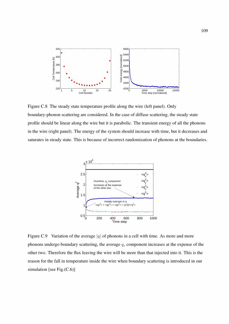
109
1 5 10 15 20220
240
260
280
300
320
Cell Number
Cel
l Tem
pera
ture
[K]
0 5000 10000 150004200
4400
4600
4800
5000
5200
5400
5600
Time step [normalized]
Tot
al e
nerg
y [n
orm
aliz
ed]
Figure C.8 The steady state temperature profile along the wire (left panel). Only
boundary-phonon scattering are considered. In the case of diffuse scattering, the steady state
profile should be linear along the wire but it is parabolic. The transient energy of all the phonons
in the wire (right panel). The energy of the system should increase with time, but it decreases and
saturates in steady state. This is because of incorrect randomization of phonons at the boundaries.
0 200 400 600 800 10000.5
1
1.5
2
2.5
3x 10
6
Time step
Ave
rage
q2
<qx2>
<qy2>
<qz2>
<q2>
Initially isotropic in q <qx2> = <qy2> = <qz2> = (1/3)*<q2>
Overtime, qz component
increases at the expenseof the other two.
Figure C.9 Variation of the average |q| of phonons in a cell with time. As more and more
phonons undergo boundary scattering, the average qz component increases at the expense of the
other two. Therefore the flux leaving the wire will be more than that injected into it. This is the
reason for the fall in temperature inside the wire when boundary scattering is introduced in our
simulation [see Fig.(C.6)]
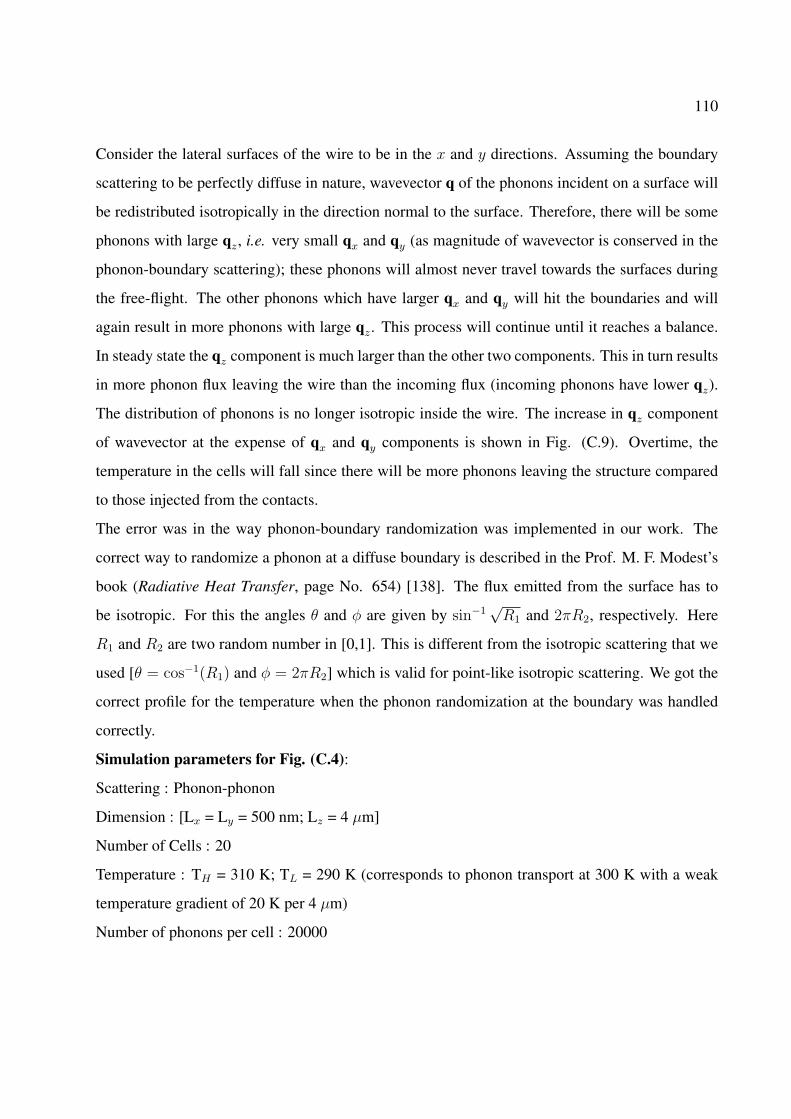
110
Consider the lateral surfaces of the wire to be in the x and y directions. Assuming the boundary
scattering to be perfectly diffuse in nature, wavevector q of the phonons incident on a surface will
be redistributed isotropically in the direction normal to the surface. Therefore, there will be some
phonons with large qz, i.e. very small qx and qy (as magnitude of wavevector is conserved in the
phonon-boundary scattering); these phonons will almost never travel towards the surfaces during
the free-flight. The other phonons which have larger qx and qy will hit the boundaries and will
again result in more phonons with large qz. This process will continue until it reaches a balance.
In steady state the qz component is much larger than the other two components. This in turn results
in more phonon flux leaving the wire than the incoming flux (incoming phonons have lower qz).
The distribution of phonons is no longer isotropic inside the wire. The increase in qz component
of wavevector at the expense of qx and qy components is shown in Fig. (C.9). Overtime, the
temperature in the cells will fall since there will be more phonons leaving the structure compared
to those injected from the contacts.
The error was in the way phonon-boundary randomization was implemented in our work. The
correct way to randomize a phonon at a diffuse boundary is described in the Prof. M. F. Modest’s
book (Radiative Heat Transfer, page No. 654) [138]. The flux emitted from the surface has to
be isotropic. For this the angles θ and φ are given by sin−1√
R1 and 2πR2, respectively. Here
R1 and R2 are two random number in [0,1]. This is different from the isotropic scattering that we
used [θ = cos−1(R1) and φ = 2πR2] which is valid for point-like isotropic scattering. We got the
correct profile for the temperature when the phonon randomization at the boundary was handled
correctly.
Simulation parameters for Fig. (C.4):
Scattering : Phonon-phonon
Dimension : [Lx = Ly = 500 nm; Lz = 4 µm]
Number of Cells : 20
Temperature : TH = 310 K; TL = 290 K (corresponds to phonon transport at 300 K with a weak
temperature gradient of 20 K per 4 µm)
Number of phonons per cell : 20000
111
Simulation parameters for Fig. (C.5):
Scattering : Phonon-phonon
Dimension : [Lx = Ly = 500 nm; Lz = 4 µm]
Number of Cells : 20
Temperature : TH = 75 K; TL = 85 K (corresponds to phonon transport at 80 K with a weak
temperature gradient of 10 K per 4 µm)
Number of phonons per cell : 20000
Simulation parameters for Fig. (C.6):
Scattering : Phonon-phonon and phonon-boundary
Dimension : [Lx = Ly = 500 nm; Lz = 4 µm]
Number of Cells : 20
Temperature : TH = 310 K; TL = 290 K (corresponds to phonon transport at 300 K with a weak
temperature gradient of 20 K per 4 µm)
Number of phonons per cell : 20000
Simulation parameters for Fig. (C.7):
Scattering : 10 × Phonon-phonon and phonon-boundary
Dimension : [Lx = Ly = 500 nm; Lz = 4 µm]
Number of Cells : 20
Temperature : TH = 310 K; TL = 290 K (corresponds to phonon transport at 300 K with a weak
temperature gradient of 20 K per 4 µm)
Number of phonons per cell : 20000
Simulation parameters for Fig. (C.8):
Scattering : phonon-boundary only
Dimension : [Lx = Ly = 500 nm; Lz = 4 µm]
Number of Cells : 20
Temperature : TH = 310 K; TL = 290 K (corresponds to phonon transport at 300 K with a weak
temperature gradient of 20 K per 4 µm)
Number of phonons per cell : 20000