thin films of copper (i) iodide doped with iodine and...
TRANSCRIPT
statu
s
soli
di
ph
ysi
ca a
Hole Conducting Materials www.pss-a.com
ORIGINAL PAPER
Thin Films of Copper (I) Iodide Doped with Iodine andThiocyanate
Landewatte Ajith DeSilva, Joshua Harwell, Anne Gaquere-Parker, Unil A. G. Perera,and Kirthi Tennakone*
It is found that thiocyanate (SCN) is an alternative dopant that greatlystabilizes the p-type semiconducting properties of CuI. Thiocyanate dopingcan be achieved by a complete removal of the excess iodine and introductionof thiocyanate via suitable precursors at ambient temperature. A method ofremoval of iodine from CuI before casting films is described. The electricaland optical properties of thiocyanate-doped CuI thin films are also discussed.
1. Introduction
Copper (I) iodide in its ambient temperature stable phaseγ-CuI is a p-type semiconductor of bandgap reported as�3.1 eV.[1–6] The high hole mobility and ease of fabricating thinfilms by different techniques makes γ-CuI a rare example of ahole conducting optically transparent material, potentiallyvaluable for opto-electronic applications.[6–8] Copper (I) iodidehas been adopted as the hole transport material in organic lightemitting diodes[9] dye-sensitized and perovskite cells,[10–12]
heterojunction diodes, and field-effect transistors.[13–15]
Thep-type semiconduction inγ-CuIdependson thepresenceofiodine in stoichiometric excess, when iodine acts as an electronacceptor generating holes in the valence band.[16] The p-typeelectrical conductivity in iodinedopedCuI is rather complexowingto volatility of iodine and dependence of conductivity on iodineconcentration. In polycrystalline CuI films, excess iodine couldpartition between grain boundaries and the bulk. If an iodine-doped CuI film deposited on glass is heated to temperature as lowas �100 �C, a part of the excess iodine escapes changing theconductivity characteristics. Again, depending on temperature
Prof. L. A. DeSilva, J. HarwellDepartment of PhysicsUniversity of West GeorgiaCarrollton, GA 30118, USA
Prof. A. Gaquere-ParkerDepartment of ChemistryUniversity of West GeorgiaCarrollton, GA 30118, USA
Prof. U. A. G. Perera, Prof. K. TennakoneDepartment of Physics and AstronomyGeorgia State UniversityAtlanta, GA 30303, USAE-mail: [email protected]
The ORCID identification number(s) for the author(s) of this articlecan be found under https://doi.org/10.1002/pssa.201700520.
DOI: 10.1002/pssa.201700520
Phys. Status Solidi A 2017, 1700520 © 21700520 (1 of 5)
and duration of storage varying amounts ofiodine accumulate in the grain boundaries.Grain boundary iodine could act as surfacedopant and the ionized donor (I�) a holetrap. Furthermore, there is evidence that themorphology of CuI polycrystalline thin-films is affected by iodine doping.[17,18]
When iodine dopant concentration is in-creased, conductivity initially increases andbegin decrease owing scattering and trap-ping by ionized donor I�, located intersti-
tially or at the grain boundaries. Recently it has been observed thatatmuchhigher iodine concentrationγ-CuI turns into a degeneratesemiconductor, reaching conductivity values above the optimumof the non-degenerate situation.[7] Presumably because of theabove features of iodine-dopedCuI, thedevicesbasedon thinfilmsof CuI do not remain stable. The first dye-sensitized solid-statesolar cell was based on CuI as a hole collector.[19] However, thestability of this device was poor, both short-circuit photocurrentandopen-circuit voltagedegradedwith timewhen the cellwaskeptexposed to light. Again, these parameters of the cell were founddecrease when the cell is stored in dark and measurementsconducted subsequently. The earlyworkers ondye-sensitized solidstate solar cells also found that the cell stability can be improved byincorporation of thiocyanate ionic liquid into the CuI coatingsolution (solution in acetonitrile) and the effect was attributed tothe functionofSCN� asa crystal growth inhibitor.[20–22] The strongadsorption of SCN� to CuI surface inhibits the growth ofcrystallite, enablingfillingpores of thenanocrystallineTiO2filmofthe heterojunction n-TiO2/Dye/p-CuI. This article describes afreshexaminationof theeffect of thiocyanateonCuI,whichrevealsthat thiocyanate (moiety SCN) acts a hole dopant inCuI, andbeingimmobile unlike I is superior to the latter and found to stabilize p-type semiconduction. Thiocyanate p-type doping of CuI isachievable, provided the stoichiometrically excess iodine is almostcompletely eliminated before introducing SCN. The note alsoindicates an extremely simple procedure for removing excessiodine from CuI, describing methods of SCN doping andcomparison of the electrical conductivity characteristics of I andSCN-doped iodine.
2. Experimental Section
Commercial (Sigma), as well as laboratory made samples of CuI,were used to prepare thin films of CuI. Commercial CuI powderis almost always partly oxidized, oxidative degradation isaggravated by light and moisture. Oxidation results in liberationof iodine via reaction in Eq. (1).
017 WILEY-VCH Verlag GmbH & Co. KGaA, Weinheim
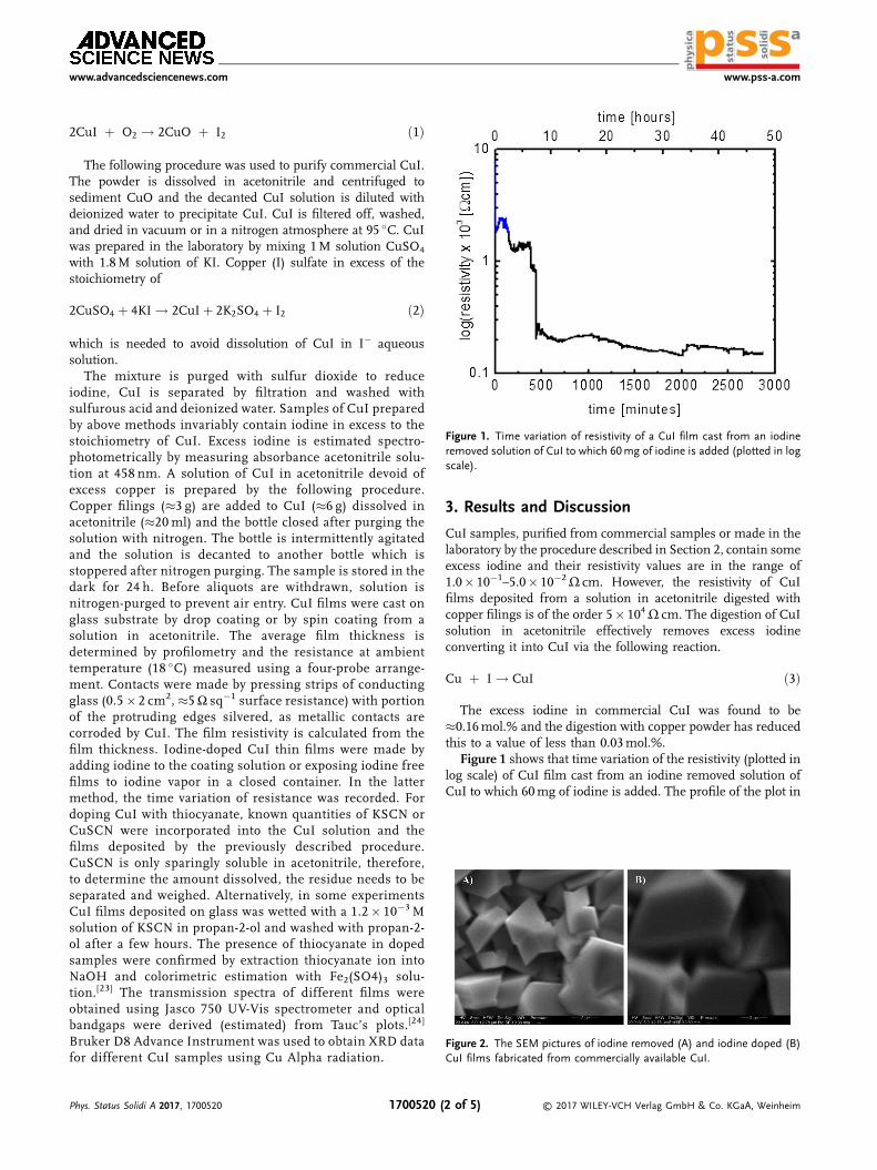
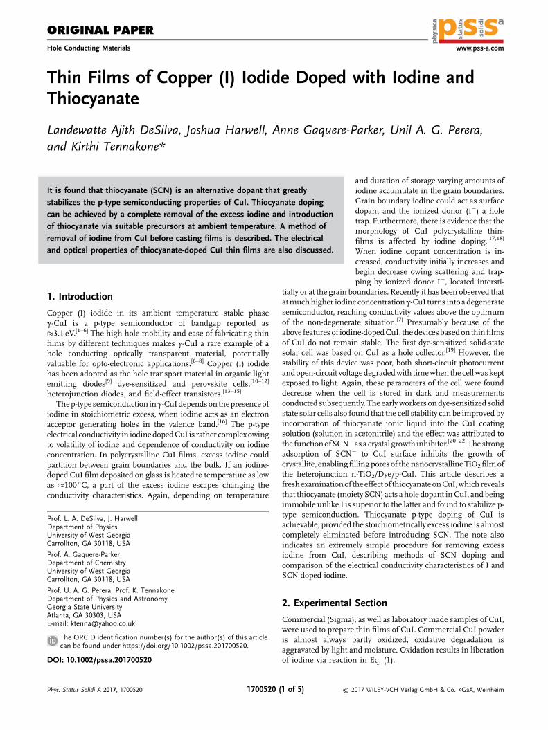
Figure 1. Time variation of resistivity of a CuI film cast from an iodineremoved solution of CuI to which 60mg of iodine is added (plotted in logscale).
Figure 2. The SEM pictures of iodine removed (A) and iodine doped (B)CuI films fabricated from commercially available CuI.
statu
s
soli
di
ph
ysi
ca a
www.advancedsciencenews.com www.pss-a.com
2CuI þ O2 ! 2CuO þ I2 ð1Þ
The following procedure was used to purify commercial CuI.The powder is dissolved in acetonitrile and centrifuged tosediment CuO and the decanted CuI solution is diluted withdeionized water to precipitate CuI. CuI is filtered off, washed,and dried in vacuum or in a nitrogen atmosphere at 95 �C. CuIwas prepared in the laboratory by mixing 1M solution CuSO4
with 1.8M solution of KI. Copper (I) sulfate in excess of thestoichiometry of
2CuSO4 þ 4KI ! 2CuIþ 2K2SO4 þ I2 ð2Þ
which is needed to avoid dissolution of CuI in I� aqueoussolution.
The mixture is purged with sulfur dioxide to reduceiodine, CuI is separated by filtration and washed withsulfurous acid and deionized water. Samples of CuI preparedby above methods invariably contain iodine in excess to thestoichiometry of CuI. Excess iodine is estimated spectro-photometrically by measuring absorbance acetonitrile solu-tion at 458 nm. A solution of CuI in acetonitrile devoid ofexcess copper is prepared by the following procedure.Copper filings (�3 g) are added to CuI (�6 g) dissolved inacetonitrile (�20ml) and the bottle closed after purging thesolution with nitrogen. The bottle is intermittently agitatedand the solution is decanted to another bottle which isstoppered after nitrogen purging. The sample is stored in thedark for 24 h. Before aliquots are withdrawn, solution isnitrogen-purged to prevent air entry. CuI films were cast onglass substrate by drop coating or by spin coating from asolution in acetonitrile. The average film thickness isdetermined by profilometry and the resistance at ambienttemperature (18 �C) measured using a four-probe arrange-ment. Contacts were made by pressing strips of conductingglass (0.5� 2 cm2, �5Ω sq�1 surface resistance) with portionof the protruding edges silvered, as metallic contacts arecorroded by CuI. The film resistivity is calculated from thefilm thickness. Iodine-doped CuI thin films were made byadding iodine to the coating solution or exposing iodine freefilms to iodine vapor in a closed container. In the lattermethod, the time variation of resistance was recorded. Fordoping CuI with thiocyanate, known quantities of KSCN orCuSCN were incorporated into the CuI solution and thefilms deposited by the previously described procedure.CuSCN is only sparingly soluble in acetonitrile, therefore,to determine the amount dissolved, the residue needs to beseparated and weighed. Alternatively, in some experimentsCuI films deposited on glass was wetted with a 1.2� 10�3 Msolution of KSCN in propan-2-ol and washed with propan-2-ol after a few hours. The presence of thiocyanate in dopedsamples were confirmed by extraction thiocyanate ion intoNaOH and colorimetric estimation with Fe2(SO4)3 solu-tion.[23] The transmission spectra of different films wereobtained using Jasco 750 UV-Vis spectrometer and opticalbandgaps were derived (estimated) from Tauc’s plots.[24]
Bruker D8 Advance Instrument was used to obtain XRD datafor different CuI samples using Cu Alpha radiation.
Phys. Status Solidi A 2017, 1700520 1700520 (
3. Results and Discussion
CuI samples, purified from commercial samples or made in thelaboratory by the procedure described in Section 2, contain someexcess iodine and their resistivity values are in the range of1.0� 10�1–5.0� 10�2Ω cm. However, the resistivity of CuIfilms deposited from a solution in acetonitrile digested withcopper filings is of the order 5� 104Ω cm. The digestion of CuIsolution in acetonitrile effectively removes excess iodineconverting it into CuI via the following reaction.
Cu þ I ! CuI ð3Þ
The excess iodine in commercial CuI was found to be�0.16mol.% and the digestion with copper powder has reducedthis to a value of less than 0.03mol.%.
Figure 1 shows that time variation of the resistivity (plotted inlog scale) of CuI film cast from an iodine removed solution ofCuI to which 60mg of iodine is added. The profile of the plot in
© 2017 WILEY-VCH Verlag GmbH & Co. KGaA, Weinheim2 of 5)
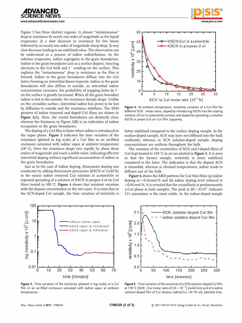
Figure 4. At ambient temperature, resistivity variation of a CuI film fordifferent SCN� molar ratios, doped by introducing KSCN into the coatingsolution of CuI in acetonitrile (circles) and doped by spreading a solutionKSCN in proan-2-ol on CuI film (squares).
statu
s
soli
di
ph
ysi
ca a
www.advancedsciencenews.com www.pss-a.com
Figure 1 has three distinct regions: 1) almost “instantaneous”drop in resistance by nearly one order of magnitude as the liquidevaporates; 2) a slow decrease in resistance for few hoursfollowed by an nearly one order of magnitude sharp drop; 3) veryslow decrease leading to an stabilized value. The observation canbe understood as a process of iodine redistribution. As thesolution evaporates, iodine segregates in the grain boundaries.Iodine in the grain boundaries acts as a surface dopant, injectingelectrons to the CuI bulk and I� residing on the surface. Thisexplains the “instantaneous” drop in resistance as the film isformed. Iodine in the grain boundaries diffuse into the CuIlattice forming an interstitial donor impurity. Iodine in the grainboundaries will also diffuse to outside, as interstitial iodineconcentration increases, the probability of trapping holes by I�
on the surface is greatly increased. When all the grain boundaryiodine is lost to the outside, the resistance sharply drops. Unlikeon the crystallite surface, interstitial iodine less prone to be lostby diffusion to outside and the resistance stabilizes. The SEMpictures of iodine removed and doped CuI films are shown inFigure 2(A). Here, the crystal boundaries are distinctly clear,whereas the fuzziness in Figure 2(B) is an indication of iodineoccupation in the grain boundaries.
The doping of a CuI film is faster when iodine is introduced inthe vapor phase. Figure 3 indicates the time variation of theresistance (plotted in log scale) of a CuI film in an air-filledenclosure saturated with iodine vapor at ambient temperature(18� C). Here the resistance drops very rapidly by about threeorders of magnitude and reach a stable value, indicating efficientinterstitial doping without significant accumulation of iodine inthe grain boundaries.
Just as in the case of iodine doping, thiocyanate doping wasconducted by adding thiocyanate precursors (KSCN or CuSCN)to the excess iodine removed CuI solution in acetonitrile orrepeated spreading of a solution of KSCN in propan-2-ol on CuIfilms heated to 105 �C. Figure 4 shows that resistant variationwith the dopant concentration in the two cases. It is seen that inthe SCN-doped CuI sample, the time variation of resistivity is
Figure 3. Time variation of the resistivity (plotted in log scale) of a CuIfilm in an air-filled enclosure saturated with iodine vapor at ambienttemperature.
Phys. Status Solidi A 2017, 1700520 1700520 (
better stabilized compared to the surface doping sample. In thesurface-doped sample, SCN may have not diffused into the bulkuniformly, whereas in SCN solution-doped sample, dopingconcentrations are uniform throughout the bulk.
The variation of the resistivities of SCN and I-doped films ofCuI kept heated to 110 �C in air are plotted in Figure 5. It is seenin that the former sample, resistivity is more stabilizedcompared to the latter. The indication is that the dopant SCNis immobile, whereas at elevated temperatures, iodine tends todiffuses out of the bulk.
Figure 6 shows the XRD patterns for CuI thin films (a) iodinedoping at� 0.16mol.% and (b) iodine doping level reduced to<0.03mol.%. It is revealed that the crystallinity is predominantlyγ-CuI phase in both samples. The peak at 2θ¼ 25.47� indicates111 orientation is the most stable. In the iodine-doped sample
Figure 5. Time variation of the resistivity of a SCN solution doped CuI filmat 110 �C (SCN�/CuI molar ratio of 2.0� 10�3) (solid line) and of a iodinesolution-doped film of CuI (excess iodine/CuI �0.1% wt) (dashed line).
© 2017 WILEY-VCH Verlag GmbH & Co. KGaA, Weinheim3 of 5)
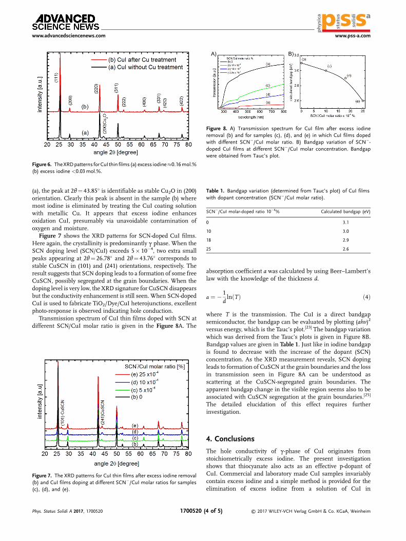
Figure 6. TheXRDpatterns forCuI thin films (a) excess iodine�0.16mol.%(b) excess iodine <0.03mol.%.
Figure 8. A) Transmission spectrum for CuI film after excess iodineremoval (b) and for samples (c), (d), and (e) in which CuI films dopedwith different SCN�/CuI molar ratio. B) Bandgap variation of SCN�-doped CuI films at different SCN�/CuI molar concentration. Bandgapwere obtained from Tauc’s plot.
Table 1. Bandgap variation (determined from Tauc’s plot) of CuI filmswith dopant concentration (SCN�/CuI molar ratio).
SCN�/CuI molar-doped ratio 10�4% Calculated bandgap (eV)
0 3.1
10 3.0
18 2.9
25 2.6
statu
s
soli
di
ph
ysi
ca a
www.advancedsciencenews.com www.pss-a.com
(a), the peak at 2θ¼ 43.85� is identifiable as stable Cu2O in (200)orientation. Clearly this peak is absent in the sample (b) wheremost iodine is eliminated by treating the CuI coating solutionwith metallic Cu. It appears that excess iodine enhancesoxidation CuI, presumably via unavoidable contamination ofoxygen and moisture.
Figure 7 shows the XRD patterns for SCN-doped CuI films.Here again, the crystallinity is predominantly γ phase. When theSCN doping level (SCN/CuI) exceeds 5� 10�4, two extra smallpeaks appearing at 2θ¼ 26.78� and 2θ¼ 43.76� corresponds tostable CuSCN in (101) and (241) orientations, respectively. Theresult suggests that SCN doping leads to a formation of some freeCuSCN, possibly segregated at the grain boundaries. When thedoping level is very low, the XRD signature for CuSCN disappearsbut the conductivity enhancement is still seen. When SCN-dopedCuI is used to fabricate TiO2/Dye/CuI heterojunctions, excellentphoto-response is observed indicating hole conduction.
Transmission spectrum of CuI thin films doped with SCN atdifferent SCN/CuI molar ratio is given in the Figure 8A. The
Figure 7. The XRD patterns for CuI thin films after excess iodine removal(b) and CuI films doping at different SCN�/CuI molar ratios for samples(c), (d), and (e).
Phys. Status Solidi A 2017, 1700520 1700520 (
absorption coefficient α was calculated by using Beer–Lambert’slaw with the knowledge of the thickness d.
α ¼ � 1dlnðTÞ ð4Þ
where T is the transmission. The CuI is a direct bandgapsemiconductor, the bandgap can be evaluated by plotting (αhν)2
versus energy, which is the Tauc’s plot.[23] The bandgap variationwhich was derived from the Tauc’s plots is given in Figure 8B.Bandgap values are given in Table 1. Just like in iodine bandgapis found to decrease with the increase of the dopant (SCN)concentration. As the XRD measurement reveals, SCN dopingleads to formation of CuSCN at the grain boundaries and the lossin transmission seen in Figure 8A can be understood asscattering at the CuSCN-segregated grain boundaries. Theapparent bandgap change in the visible region seems also to beassociated with CuSCN segregation at the grain boundaries.[25]
The detailed elucidation of this effect requires furtherinvestigation.
4. Conclusions
The hole conductivity of γ-phase of CuI originates fromstoichiometrically excess iodine. The present investigationshows that thiocyanate also acts as an effective p-dopant ofCuI. Commercial and laboratory made CuI samples invariablycontain excess iodine and a simple method is provided for theelimination of excess iodine from a solution of CuI in
© 2017 WILEY-VCH Verlag GmbH & Co. KGaA, Weinheim4 of 5)
statu
s
soli
di
ph
ysi
ca a
www.advancedsciencenews.com www.pss-a.com
acetonitrile. Thiocynate doping can be carried out by introducinga thiocyanate precursor into the coating solution or spreading aprecursor solution over thin-films of CuI. Unlike iodine, dopedthiocyanate is immobile and is not lost during thermalprocessing or storage of CuI films. The investigation alsorevealed that excess iodine in CuI enhances the oxidation of CuI.As expected, thiocyanate-doped CuI exhibits higher thermalstability compared to iodine-doped films. As thiocyanatedoping of CuI after iodine removal yields more stable films,experiments are underway to use the material as hole collectorsin dye-sensitized solar cells and also determines hole mobilitiesin the films under different conditions.
AcknowledgmentsFinancial support from UWG SRAP, COSM FRG, and SEEP programs areacknowledged. Help provided by Dr. Madhavi Thakurdesai, Birla Collage,Kalyan India with getting XRD data is also acknowledged.
Conflict of InterestThe authors declare no conflict of interest.
Keywordscopper iodide, hole conducting materials, thiocyanate doping,transparent semiconductors
Received: July 24, 2017Revised: September 26, 2017
Published online:
[1] J. X. M. Zheng-Johansson, I. Ebbsjö, R. L. McGreevy, Solid State Ion.1995, 82, 115.
[2] J. X. M. Zheng-Johansson, R. L. McGreevy, Solid State Ion. 1996,83, 35.
[3] D. A. Keen, S. Hull, J. Phys.: Condens. Matter 1994, 6, 1637.
Phys. Status Solidi A 2017, 1700520 1700520 (
[4] W. Bührer, W. Hälg, Electrochim. Acta 1977, 22, 701.[5] K. Tennakone, G. R. R. A. Kumara, A. R. Kumarasinghe,
P. M. Sirimanna, J. Photochem. Photobiol. 1996, 96, 167.[6] M. Grundmann, F.-L. Schein, M. Lorenz, T. Böntgen, J. Lenzner,
H. von Wenckstern, Phys. Status Solidi A 2013, 210, 1671.[7] C. Yang, M. Kneiβ, M. Lorenz, M. Grundmann, Proc. Natl. Acad. Sci.
USA 2016, 113, 12929.[8] N. Yamada, R. Ino, Y. Ninomiya, Chem. Mater. 2016, 28, 4971.[9] M. Shan, H. Jiang, Y. Guan, D. Sun, Y. Wang, J. Hua, J. Wang, RSC
Adv. 2017, 7, 13584.[10] K. Tennakone, G. R. R. A. Kumara, K. G. U. Wijayantha, Semicond. Sci.
Technol. 1996, 11, 1737.[11] Y. Zhou, T. Taima, T. Miyadera, T. Yamanari, M. Kitamura,
K. Nakatsu, Y. Yoshida, Nano Lett. 2012, 8, 4146.[12] P. M. Sirimanne, V. P. S. Perera, Phys. Status Solidi B 2008, 245,
1828.[13] G. A. Sepalage, S. Meyer, A. Pascoe, A. D. Scully, F. Huang, U. Bach,
Y.-B. Cheng, L. Spiccia, Adv. Funct. Mater. 2015, 25, 5650.[14] C. Yang, M. Kneiß, F.-L. Schein, M. Lorenz, M. Grundmann, Sci. Rep.
2016, 6, 21937.[15] F.-L. Scheina, H. von Wenckstern, M. Grundmann, Appl. Phys. Lett.
2013, 102, 092109.[16] K. Tennakone, G. R. R. A. Kumara, I. R. M. Kottegoda, V. P. S. Perera,
G. M. L. P. Aponsu, K. G. U. Wijayantha, Sol. Energy Mater. Sol. Cells1998, 55, 283.
[17] M. N. Amalina, Y. Azilawatia, N. A. Rasheida, M. Rusop, Proc. Eng.2013, 56, 731.
[18] C. Moditswe, C. M. Muiva, P. Luhanga, A. Juma, Ceram. Int. 2017, 43,5126.
[19] K. Tennakone, G. R. R. A. Kumara, A. R. Kumarasinghe,K. G. U. Wijayantha, P. M. Sirimanne, Semicond. Sci. Technol.1995, 10, 1689.
[20] V. P. S. Perera, M. K. I. Senevirathna, P. K. D. D. P. Pitigala,K. Tennakone, Sol. Energy Mater. Sol. Cells 2005, 86, 443.
[21] V. P. S. Perera, P. K. D. D. P. Pitigala, P. V. V. Jayaweera,K. M. P. Bandaranayake, K. Tennakone, J. Phys. Chem. B 2003, 107,13758.
[22] V. V. Giridhar, C. Kalidas, J. Solution Chem. 1982, 11, 539.[23] F. Nyasulu, R. Barlag, J. Chem. Educ. 2011, 88, 313.[24] J. Tauc, R. Grigorovici, A. Vancu, Phys. Status Solidi 1966, 15,
627.[25] M. N. Amalina, N. A. Rasheid, M. Rusop, J. Nanomater. 2012, 2012,
637637.
© 2017 WILEY-VCH Verlag GmbH & Co. KGaA, Weinheim5 of 5)