third year progress report & final report - … · third year progress report & final...
TRANSCRIPT

SAMBA
Third Year Progress Report & Final Report
Delivered May 2004
2
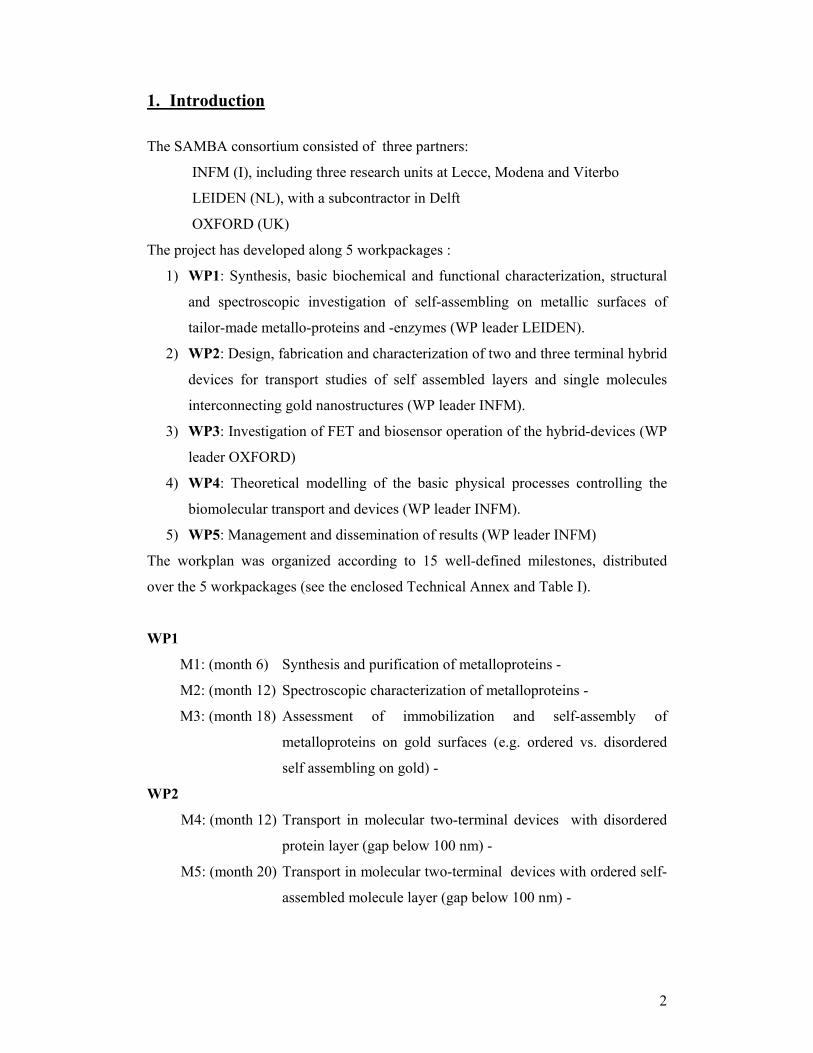
1. Introduction The SAMBA consortium consisted of three partners:
INFM (I), including three research units at Lecce, Modena and Viterbo
LEIDEN (NL), with a subcontractor in Delft
OXFORD (UK)
The project has developed along 5 workpackages :
1) WP1: Synthesis, basic biochemical and functional characterization, structural
and spectroscopic investigation of self-assembling on metallic surfaces of
tailor-made metallo-proteins and -enzymes (WP leader LEIDEN).
2) WP2: Design, fabrication and characterization of two and three terminal hybrid
devices for transport studies of self assembled layers and single molecules
interconnecting gold nanostructures (WP leader INFM).
3) WP3: Investigation of FET and biosensor operation of the hybrid-devices (WP
leader OXFORD)
4) WP4: Theoretical modelling of the basic physical processes controlling the
biomolecular transport and devices (WP leader INFM).
5) WP5: Management and dissemination of results (WP leader INFM)
The workplan was organized according to 15 well-defined milestones, distributed
over the 5 workpackages (see the enclosed Technical Annex and Table I).
WP1
M1: (month 6) Synthesis and purification of metalloproteins -
M2: (month 12) Spectroscopic characterization of metalloproteins -
M3: (month 18) Assessment of immobilization and self-assembly of
metalloproteins on gold surfaces (e.g. ordered vs. disordered
self assembling on gold) -
WP2
M4: (month 12) Transport in molecular two-terminal devices with disordered
protein layer (gap below 100 nm) -
M5: (month 20) Transport in molecular two-terminal devices with ordered self-
assembled molecule layer (gap below 100 nm) -
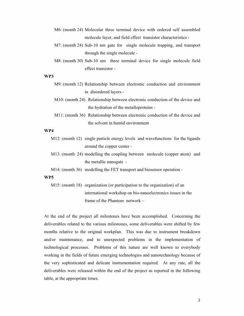
3
M6: (month 24) Molecular three terminal device with ordered self assembled
molecule layer, and field effect transistor characteristics -
M7: (month 24) Sub-10 nm gate for single molecule trapping, and transport
through the single molecule -
M8: (month 30) Sub-10 nm three terminal device for single molecule field
effect transistor -
WP3
M9: (month 12) Relationship between electronic conduction and environment
in disordered layers -
M10: (month 24) Relationship between electronic conduction of the device and
the hydration of the metalloproteins -
M11: (month 36) Relationship between electronic conduction of the device and
the solvent in humid environment
WP4
M12: (month 12) single particle energy levels and wavefunctions for the ligands
around the copper center -
M13: (month 24) modelling the coupling between molecule (copper atom) and
the metallic nanogate -
M14: (month 36) modelling the FET transport and biosensor operation -
WP5
M15: (month 18) organization (or participation to the organization) of an
international workshop on bio-nanoelectronics issues in the
frame of the Phantom network –
At the end of the project all milestones have been accomplished. Concerning the
deliverables related to the various milestones, some deliverables were shifted by few
months relative to the original workplan. This was due to instrument breakdown
and/or maintenance, and to unexpected problems in the implementation of
technological processes. Problems of this nature are well known to everybody
working in the fields of future emerging technologies and nanotechnology because of
the very sophisticated and delicate instrumentation required. At any rate, all the
deliverables were released within the end of the project as reported in the following
table, at the appropriate times.
4
This report summarises the work carried out during the third and last year, and was
prepared following the list of Milestones and Deliverables promised by the different
partners at the end of the project (see Table II for a list of the deliverables expected
for month 36). In addition, we will address some open questions concerning the
completion of milestones M6 , M7, and M13 and some criticisms raised in the 2003
reviewing round (June 2003, Brussels) resulting in a number of additional
experiments not listed in the project initial description.
For details of the results concerning the activity of the first two years of the project we
refer to the last two activity and progress reports (see enclosed files)
2.General assessment of the project 2.1 Final remarks on the results achieved within the project research activity
and collaborations.
There was generally good collaboration amongst the partners, with fruitful
exchanges through project meetings and by e-mail. The collaborations resulted in a
large number of joint publications. A number of them are in press or still in preparation.
The project also offered the chance to form a number of young researchers.
The work performed during the three years of the SAMBA project has given us
the possibility to explore a new exciting field, and to develop and disseminate new
methodologies and new knowledge at the boundary between Nanotechnology and
Biology/Biochemistry. Several of the research lines will have a natural continuation,
and particularly: (i) the realisation of new-generation, single-molecule three-terminal
devices; (ii.) the computation of the electron transfer rate for the dimer proposed by
the Leiden group, combining the computed reorganization energy and transfer
integrals; (iii) the refinement of the model for the protein-layer transistor; (iv) other
specific investigations that will follow-up novel experimental outcomes related to
electron-transfer proteins; (v) ab-initio computation of electric-field-gradient
parameters that are able to shed further light onto the electronic structure of the active
site (collaboration between ONFM-Modena and a Brazilian group external to the
SAMBA partnership) Moreover, the new expertise and know-how that we have
developed has offered the chance to start new research lines and collaborations and to
propose new projects in the area of nanobiotecnology to both the Italian MIUR and
5
the EC. These will include: (i.) lab-on-chip devices for genomics and postgenomics;
(ii.) desing of novel molecular architectures through bio self-assembly;. (iii.)
molecular computation. Moreover as a consequence of the dissemination of the
results in several domestic and international conferences, schools and workshop (on
both biomolecule chemisorption onto solid substrates and electronic detection of
small bioelectronic signals) an international microelectronic Company (ST-
Microelctronics) has started an R&D project and a joint laboratory at the NNL
laboratory (Lecce) to build a new generation of LabOnChip devices.
2.2 Exchange of students/researchers and meetings in the third year
Several short visits (1-2 weeks) were exchanged among the partners. Staff
members and various students from Oxford, Lecce and Viterbo visited the Leiden
group for periods ranging from 1 week to 8 months. One of the students from INFM
finished her PhD degree in Leiden, and also spent a considerable length of time at
Oxford. Conversely, staff and students from Leiden visited Lecce, Modena and
Viterbo a number of times. One PhD student and one postdoc from Leiden have spent
a month in Oxford, and one postdoc from Oxford visited the Leiden group. Repeated
staff visits were exchanged between INFM-Modena and INFM-Lecce.
Three general meetings were organized in Brussels and Lecce, where the
partners met to coordinate the collaboration. In addition, an international workshop
was organized (see enclosed brochure for the list of speakers and titles of
presentations)
A project WEB-page was published on www.samba-project.it and regularly
updated . SAMBA gained recognition as one of the major initiatives in the
framework of the PHANTOMS network, as highlighted both on the Phantoms WWW
and on the information CD.
6
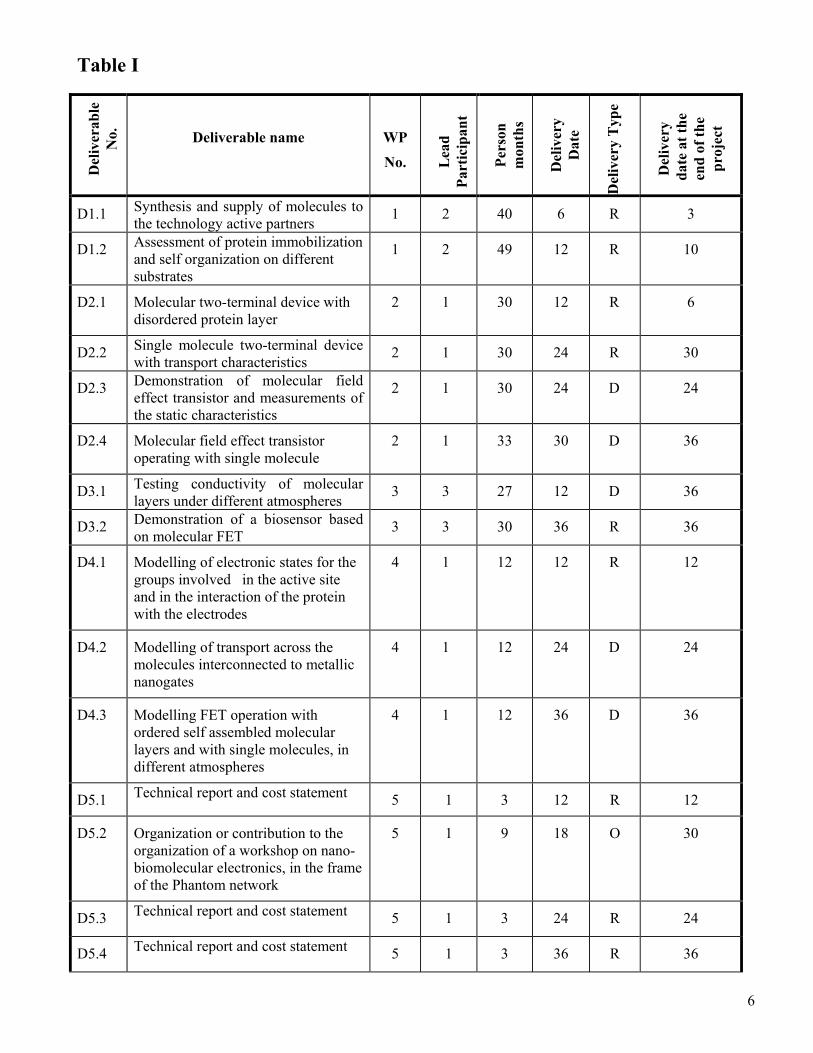
Table I
Del
iver
able
N
o.
Deliverable name
WP
No. Lea
d Pa
rtic
ipan
t
Pers
on
mon
ths
Del
iver
y D
ate
Del
iver
y T
ype
Del
iver
y
dat
e at
the
end
of th
e pr
ojec
t
D1.1 Synthesis and supply of molecules to the technology active partners 1 2 40 6 R 3
D1.2 Assessment of protein immobilization and self organization on different substrates
1 2 49 12 R 10
D2.1 Molecular two-terminal device with disordered protein layer
2 1 30 12 R 6
D2.2 Single molecule two-terminal device with transport characteristics 2 1 30 24 R 30
D2.3 Demonstration of molecular field effect transistor and measurements of the static characteristics
2 1 30 24 D 24
D2.4 Molecular field effect transistor operating with single molecule
2 1 33 30 D 36
D3.1 Testing conductivity of molecular layers under different atmospheres 3 3 27 12 D 36
D3.2 Demonstration of a biosensor based on molecular FET 3 3 30 36 R 36
D4.1 Modelling of electronic states for the groups involved in the active site and in the interaction of the protein with the electrodes
4 1 12 12 R 12
D4.2 Modelling of transport across the molecules interconnected to metallic nanogates
4 1 12 24 D 24
D4.3 Modelling FET operation with ordered self assembled molecular layers and with single molecules, in different atmospheres
4 1 12 36 D 36
D5.1 Technical report and cost statement 5 1 3 12 R 12
D5.2 Organization or contribution to the organization of a workshop on nano-biomolecular electronics, in the frame of the Phantom network
5 1 9 18 O 30
D5.3 Technical report and cost statement 5 1 3 24 R 24
D5.4 Technical report and cost statement 5 1 3 36 R 36
7
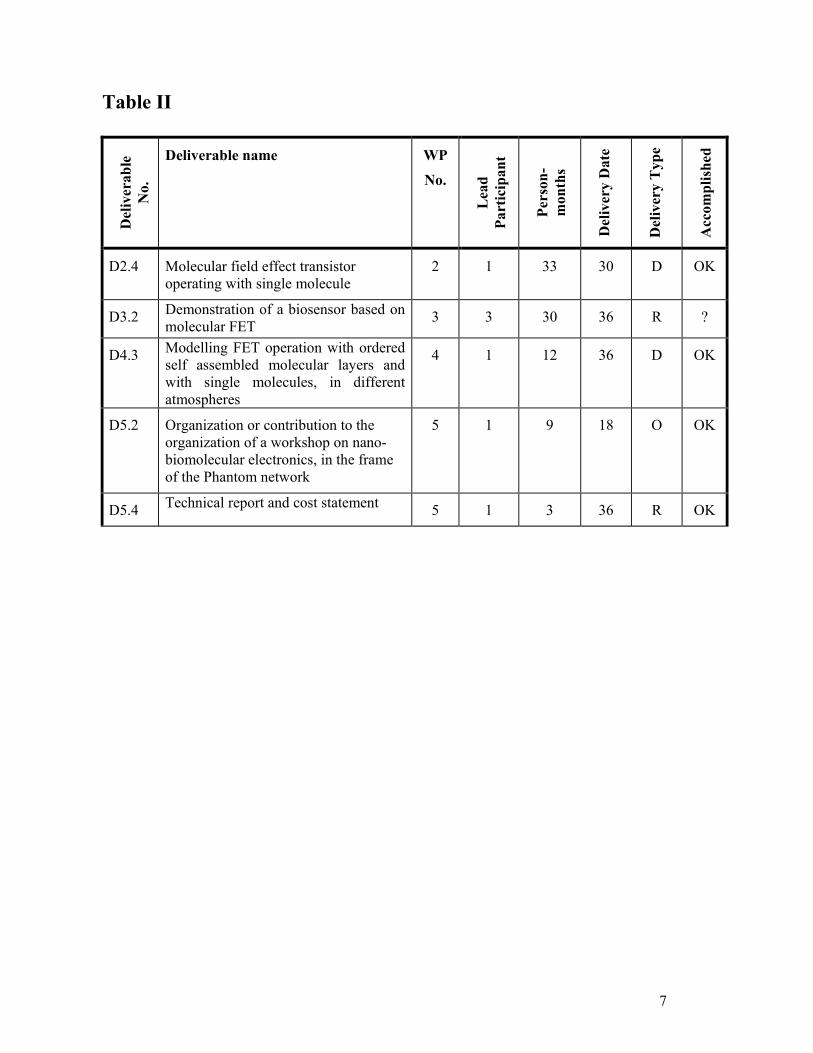
Table II
Del
iver
able
N
o.
Deliverable name WP
No.
Lea
d Pa
rtic
ipan
t
Pers
on-
mon
ths
Del
iver
y D
ate
Del
iver
y T
ype
Acc
ompl
ishe
d
D2.4 Molecular field effect transistor operating with single molecule
2 1 33 30 D OK
D3.2 Demonstration of a biosensor based on molecular FET 3 3 30 36 R ?
D4.3 Modelling FET operation with ordered self assembled molecular layers and with single molecules, in different atmospheres
4 1 12 36 D OK
D5.2 Organization or contribution to the organization of a workshop on nano-biomolecular electronics, in the frame of the Phantom network
5 1 9 18 O OK
D5.4 Technical report and cost statement 5 1 3 36 R OK
8
3.1 WP1 (Leiden)
The Leiden contribution to SAMBA concentrated on the development,
production and characterisation of protein and enzyme variants. The design of new
variants was usually based on extensive modeling. Construction at the DNA-level was
achieved by modern state-of the-art recombinant DNA techniques. Expression and
purification of the proteins/enzymes was achieved according to advanced protein
chemistry techniques. Purification protocols were developed or adjusted where
necessary. Characterisation of the proteins/enzymes was achieved by standard
biochemical techniques. Spectroscopic characterisation involved UV-VIS
spectroscopy, mass spec analysis, protein film voltammetry, cyclic voltammetry and,
when necessary, EPR and NMR spectroscopy. Activity was checked by enzymological
and kinetic techniques (stopped flow, NMR). At a later stage of the project
proteins/enzymes were also characterised for their behaviour on solid supports (gold,
mica, carbon) by means of atomic force microscopy (AFM) both under ambient
conditions and in situ.
3.1.1 DEVELOPMENT AND PRODUCTION OF VARIANTS
The group in Leiden, in collaboration with the subcontractor from Delft
University of Technology, has developed, produced and made available to the
partners within the framework of WP1, 2 and 3 the suite of electron-transfer
metalloproteins and metalloprotein enzymes listed in Table I. They were used for
immobilisation on solid surfaces, the study of their electrochemical and electronic
behaviour, and characterisation by scanning probe techniques. Both wild type proteins
and variants in their Cu, Zn, and apo forms have been expressed, purified,
characterized and shipped to INFM Viterbo, INFM Modena, INFM Lecce and
Oxford. In addition fern plastocyanin variants (w.t., F12L, G36P, F12LG36P) were
made available to the group of Prof. Takamitsu Kozhuma at Ibaraki University, Mito,
Japan, and S. antibioticus tyrosinase to the group of Prof. Shun Hiroata, Kyoto
University, to strengthen the visibility of the European research in the field, as set out
in WP5 .
A number of the ET proteins listed in Table 1 are physiological partners of the
enzymes listed in the lower half of this table. This was a consideration when choosing
the proteins for the present study, since emphasis was placed on enhancing the
chances for optimal ET rates at the electrode when using enzymes. One of the issues
9
we wanted to explore was the possibility of preparing a surface with a monolayer of
an ET protein that could act as an optimal surface for the enzyme to react with.
Examples of pairs of partners are haem containing peroxidase/cytochrome c, copper
containing nitrite reductase/peseudo-azurin, methylamine dehydrogenase/amicyanin,
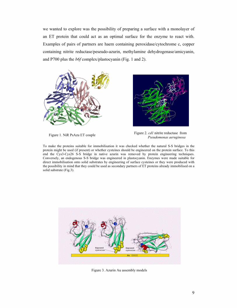
and P700 plus the b6f complex/plastocyanin (Fig. 1 and 2).
To make the proteins suitable for immobilisation it was checked whether the natural S-S bridges in the protein might be used (if present) or whether cysteines should be engineered on the protein surface. To this end the Cys3-Cys26 S-S bridge in native azurin was removed by protein engineering techniques. Conversely, an endogenous S-S bridge was engineered in plastocyanin. Enzymes were made suitable for direct immobilisation onto solid substrates by engineering of surface cysteines or they were produced with the possibility in mind that they could be used as secondary partners of ET proteins already immobilised on a solid substrate (Fig.3).
Figure 1. NiR PsAzu ET couple Figure 2. cd1 nitrite reductase from Pseudomonas aeruginosa
Figure 3. Azurin Au assembly models
10
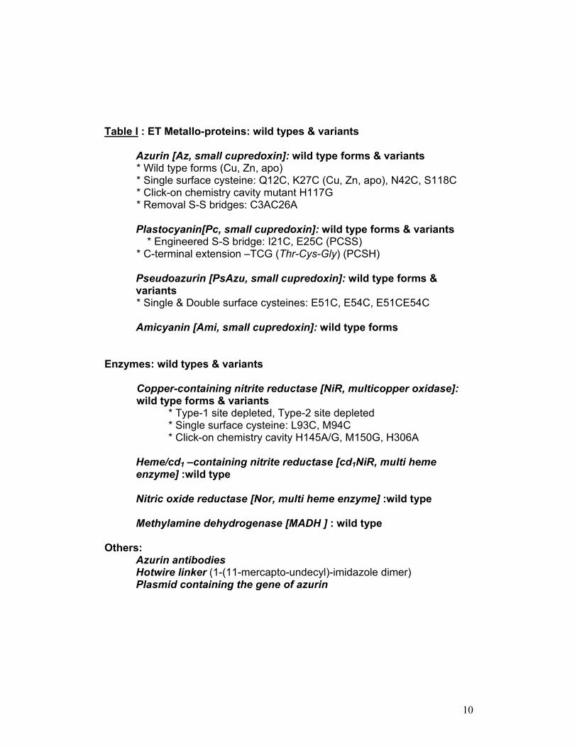
Table I : ET Metallo-proteins: wild types & variants
Azurin [Az, small cupredoxin]: wild type forms & variants * Wild type forms (Cu, Zn, apo) * Single surface cysteine: Q12C, K27C (Cu, Zn, apo), N42C, S118C * Click-on chemistry cavity mutant H117G * Removal S-S bridges: C3AC26A Plastocyanin[Pc, small cupredoxin]: wild type forms & variants
* Engineered S-S bridge: I21C, E25C (PCSS) * C-terminal extension –TCG (Thr-Cys-Gly) (PCSH) Pseudoazurin [PsAzu, small cupredoxin]: wild type forms & variants * Single & Double surface cysteines: E51C, E54C, E51CE54C Amicyanin [Ami, small cupredoxin]: wild type forms
Enzymes: wild types & variants Copper-containing nitrite reductase [NiR, multicopper oxidase]: wild type forms & variants
* Type-1 site depleted, Type-2 site depleted * Single surface cysteine: L93C, M94C * Click-on chemistry cavity H145A/G, M150G, H306A Heme/cd1 –containing nitrite reductase [cd1NiR, multi heme enzyme] :wild type Nitric oxide reductase [Nor, multi heme enzyme] :wild type Methylamine dehydrogenase [MADH ] : wild type
Others: Azurin antibodies Hotwire linker (1-(11-mercapto-undecyl)-imidazole dimer) Plasmid containing the gene of azurin
11
Finally, azurin and pseudo-azurin were engineered with more than one surface
cysteine to check if immobilisation could be improved when more than one point of
surface attachment would was available. Mutants were designed with different sets of
anchoring cysteines positioned on the side or on the south end of the proteins, thus
allowing more precise control of the orientation and flexibility of the protein.
One of the major setbacks during production of cysteine containing protein
variants is that copper can catalyse non-specific disulfide bridge formation, which
renders purification more difficult. Moreover, expressed protein, depending on the
individual mutant and the batch, may contain as much as 80% Zn in the active site
instead of the more desired Cu. Extraction of Zn ion can only be achieved by means
of unfolding, which results in large losses of protein. To increase the final yield of the
desired form of azurin, the gene of the wild type azurin and a small sub-set of the
cysteine-containing mutants were upgraded from the pUC19 vector to the pET28
vector, which usually exhibits a higher expression level. Purification protocols for
these variants have been developed taking into account the need to control the
monomeric/ dimeric ratio of the proteins. The apo- and Zn forms of the blue copper
proteins were engineered with the specific goal to investigate the effect of removing
or replacing the Cu in the active site with a redox inactive metal.
With respect to this panel of generated protein variants, those with the surface-
exposed cysteines showed a high degree of similarity with the native parent forms in
spectral/ structural behaviour as analysed with UV-vis & EPR spectroscopy and with
X-ray diffraction. In addition their redox properties in solution did not significantly
differ from their respective wild type forms.
3.1.2 CAVITY MUTANTS
Cavity mutants of azurin and nitrite reductase weredesigned to facilitate direct
connection of the active redox site to the electrode by so-called hot wires. Residues
constituting the copper sites are replaced by amino acids creating a gap in the ligand
shell of the copper. In general the cavity mutants need to be reconstituted with an
(external, click-on) ligand to obtain their native-like properties. Interestingly, the
creation of a cavity involving the axial ligand of the copper site, i.e. Met-150 in NiR
or Met-121 in Az, affects the features of the redox sites to a much lesser extent than
the ones involving the surface-exposed His-145 in NiR and His-117 in Az. However,
from the point of view of introducing the most effective (shortest) linker-ligand
12
assembly between the protein redox site and the electrode, the latter mutation, i.e., the
one involving the exposed His, is preferable.
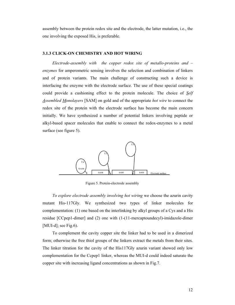
3.1.3 CLICK-ON CHEMISTRY AND HOT WIRING
Electrode-assembly with the copper redox site of metallo-proteins and –
enzymes for amperometric sensing involves the selection and combination of linkers
and of protein variants. The main challenge of constructing such a device is
interfacing the enzyme with the electrode surface. The use of these special coatings
could provide a cushioning effect to the protein molecule. The choice of Self
Assembled Monolayers [SAM] on gold and of the appropriate hot wire to connect the
redox site of the protein with the electrode surface has become the main concern
initially. We have synthesized a number of potential linkers involving peptide or
alkyl-based spacer molecules that enable to connect the redox-enzymes to a metal
surface (see figure 5).
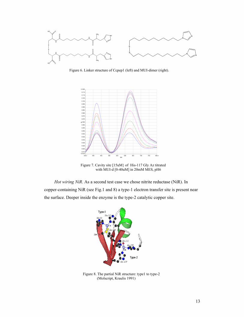
To explore electrode assembly involving hot wiring we choose the azurin cavity
mutant His-117Gly. We synthesized two types of linker molecules for
complementation: (1) one based on the interlinking by alkyl groups of a Cys and a His
residue [CCpep1-dimer] and (2) one with (1-(11-mercaptoundecyl)-imidazole-dimer
[MUI-d]; see Fig.6).
To complement the cavity copper site the linker had to be used in a dimerized
form; otherwise the free thiol groups of the linkers extract the metals from their sites.
The linker titration for the cavity of the His117Gly azurin variant showed only low
complementation for the Ccpep1 linker, whereas the MUI-d could indeed saturate the
copper site with increasing ligand concentrations as shown in Fig.7.
Figure 5. Protein-electrode assembly
13
Hot wiring NiR. As a second test case we chose nitrite reductase (NiR). In
copper-containing NiR (see Fig.1 and 8) a type-1 electron transfer site is present near
the surface. Deeper inside the enzyme is the type-2 catalytic copper site.
Figure 7. Cavity site [15uM of His-117 Gly Az titrated with MUI-d [0-40uM] in 20mM MES, pH6
350.0 400 450 500 550 600 650 700 750 800.00.01200.015
0.020
0.025
0.030
0.035
0.040
0.045
0.050
0.055
0.060
0.065
0.070
0.075
0.080
0.085
0.090
0.095
0.100
0.105
0.110
0.115
0.1200
NM
A
Figure 8. The partial NiR structure: type1 to type-2 (Molscript, Kraulis 1991)
HN
NH
N
NH2
O
NH
OHO
O
NH
NH
N
NH2
O
HN
OHO
O
S
S
NN
S
NN
S
Figure 6. Linker structure of Ccpep1 (left) and MUI-dimer (right).
14
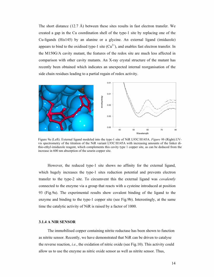
The short distance (12.7 Å) between these sites results in fast electron transfer. We
created a gap in the Cu coordination shell of the type-1 site by replacing one of the
Cu-ligands (His145) by an alanine or a glycine. An external ligand (imidazole)
appears to bind to the oxidised type-1 site (Cu2+), and enables fast electron transfer. In
the M150G/A cavity mutant, the features of the redox site are much less affected in
comparison with other cavity mutants. An X-ray crystal structure of the mutant has
recently been obtained which indicates an unexpected internal reorganisation of the
side chain residues leading to a partial regain of redox activity.
However, the reduced type-1 site shows no affinity for the external ligand,
which hugely increases the type-1 sites reduction potential and prevents electron
transfer to the type-2 site. To circumvent this the external ligand was covalently
connected to the enzyme via a group that reacts with a cysteine introduced at position
93 (Fig.9a). The experimental results show covalent binding of the ligand to the
enzyme and binding to the type-1 copper site (see Fig.9b). Interestingly, at the same
time the catalytic activity of NiR is raised by a factor of 1000.
3.1.4 A NIR SENSOR
The immobilised copper containing nitrite reductase has been shown to function
as nitrite sensor. Recently, we have demonstrated that NiR can be driven to catalyse
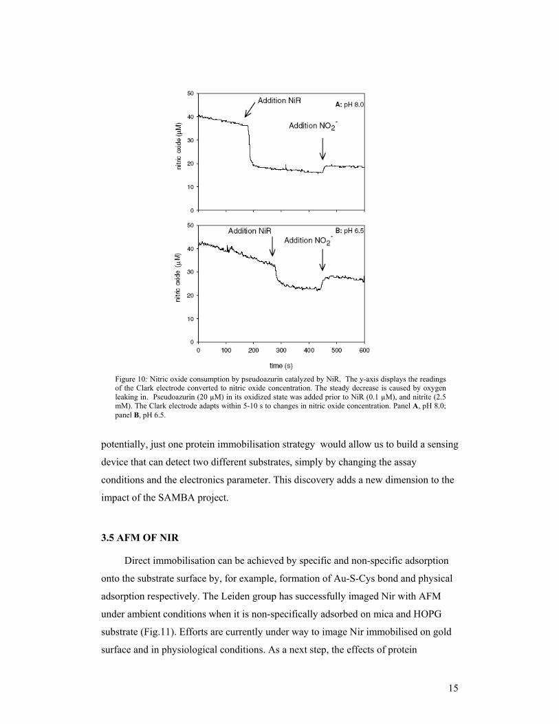
the reverse reaction, i.e., the oxidation of nitric oxide (see Fig.10). This activity could
allow us to use the enzyme as nitric oxide sensor as well as nitrite sensor. Thus,
Wavelength 40 50 60 70 80
Absorbance
0.00
0.00
0.00
0.01
0.01
Figure 9a (Left). External ligand modeled into the type-1 site of NiR L93C/H145A. Figure 9b (Right).UV-vis spectrometry of the titration of the NiR variant L93C/H145A with increasing amounts of the linker di-thio-ethyl-imidazole reagent, which complements this cavity type 1 copper site, as can be deduced from theincrease in 600 nm absorption of the azurin copper site.
15
potentially, just one protein immobilisation strategy would allow us to build a sensing
device that can detect two different substrates, simply by changing the assay
conditions and the electronics parameter. This discovery adds a new dimension to the
impact of the SAMBA project.
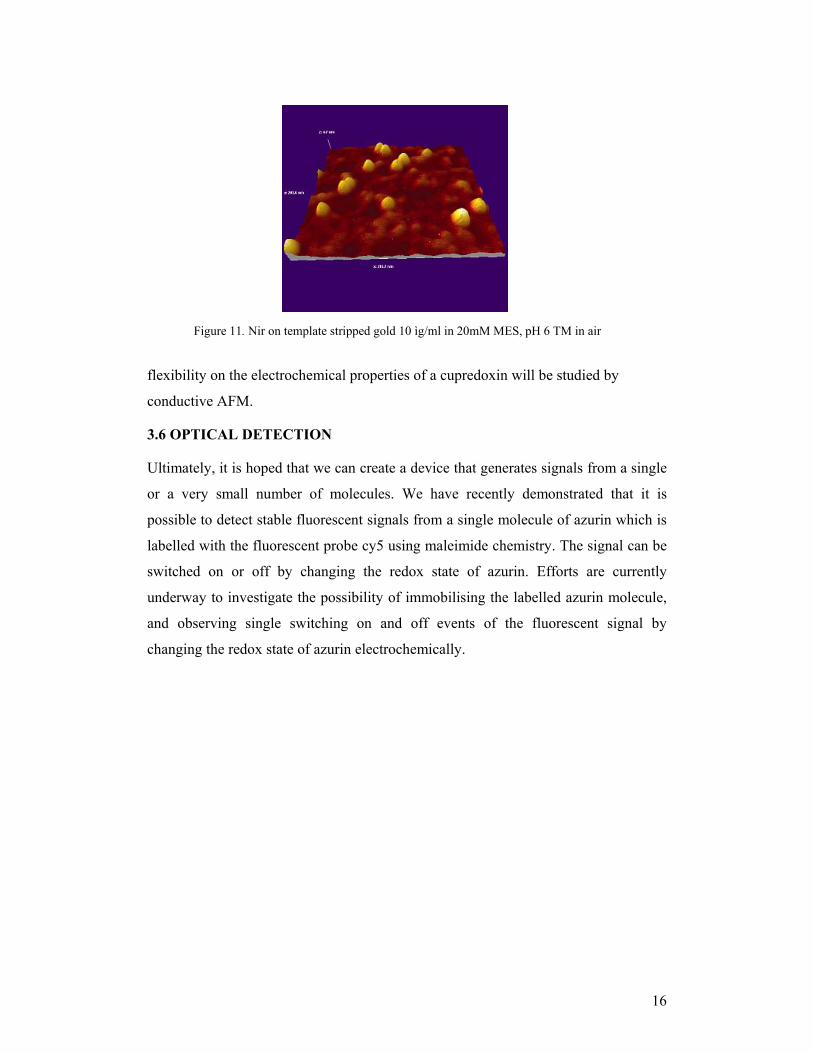
3.5 AFM OF NIR
Direct immobilisation can be achieved by specific and non-specific adsorption
onto the substrate surface by, for example, formation of Au-S-Cys bond and physical
adsorption respectively. The Leiden group has successfully imaged Nir with AFM
under ambient conditions when it is non-specifically adsorbed on mica and HOPG
substrate (Fig.11). Efforts are currently under way to image Nir immobilised on gold
surface and in physiological conditions. As a next step, the effects of protein
Figure 10: Nitric oxide consumption by pseudoazurin catalyzed by NiR. The y-axis displays the readingsof the Clark electrode converted to nitric oxide concentration. The steady decrease is caused by oxygenleaking in. Pseudoazurin (20 µM) in its oxidized state was added prior to NiR (0.1 µM), and nitrite (2.5mM). The Clark electrode adapts within 5-10 s to changes in nitric oxide concentration. Panel A, pH 8.0;panel B, pH 6.5.
16
flexibility on the electrochemical properties of a cupredoxin will be studied by
conductive AFM.
3.6 OPTICAL DETECTION
Ultimately, it is hoped that we can create a device that generates signals from a single
or a very small number of molecules. We have recently demonstrated that it is
possible to detect stable fluorescent signals from a single molecule of azurin which is
labelled with the fluorescent probe cy5 using maleimide chemistry. The signal can be
switched on or off by changing the redox state of azurin. Efforts are currently
underway to investigate the possibility of immobilising the labelled azurin molecule,
and observing single switching on and off events of the fluorescent signal by
changing the redox state of azurin electrochemically.
Figure 11. Nir on template stripped gold 10 ìg/ml in 20mM MES, pH 6 TM in air
17
3.2 WP2 3.2.1 Completion of M6 : Molecular three terminal device with ordered self
assembled molecule layer, and field effect transistor characteristics (INFM-Lecce)
3.2.1a Protein devices Different molecular devices were fabricated based on: 1. commercial azurin, purchased by Sigma Aldrich, with a copper atom inside.
2. azurins supplied by the Metalloprotein & Protein Engineering Group at the Leiden
University including: i.) recombinant azurin (Az-Cu), again a copper protein but
exhibiting a higher degree of purity; ii.) a modified azurin with a Zn atom inside
(Az-Zn); iii.) apo-azurin (Az-Apo) without any metal atom, in order to assess its
role.
3. reference devices, including empty nanojunctions and devices that were silanised
or completely functionalized but with no added protein.
Protein Field-Effect Transistors based on self-assembled monolayers of copper azurin. For this study, both the source-drain separation and the oxide thickness were 100 nm
and arrow-shaped Cr/Au planar electrodes were employed. Current-voltage
experiments were carried out by using a semiconductor parameter analyzer (HP
Agilent 4155B) in the voltage range between –6 and 6 volts (drain-source voltage), at
room temperature and ambient pressure. The gate voltage (Vg) was changed in order
to investigate its influence on the current (Ids) between the source (s) and drain (d)
electrodes. Protein immobilization on Si/SiO2 substrates was achieved (as previously
described) using a two-step procedure involving (a) the self-assembly of 3-
mercaptopropyltrimethoxysilane (3-MPTS) and (b) the reaction of the free thiol
groups of 3-MPTS with the surface disulfide bridge of Az, which is broken to form a
covalent bond to the silane-functionalized Si/SiO2 substrate. As a consequence, an
oriented monolayer is formed, i.e. a monolayer in which all the proteins have the
same orientation with respect to the substrate, due to the presence of just one disulfide
bond, i.e. a unique linking site, in the protein. Since protein adsorption on surfaces
may lead to denaturation, we examined the protein shape and fold pattern after
immobilization, as described in section 3.2.1b)
18
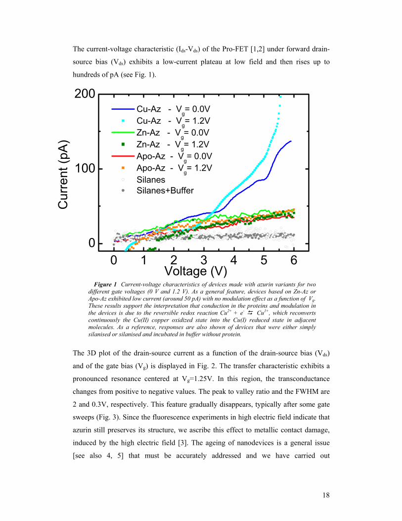
The current-voltage characteristic (Ids-Vds) of the Pro-FET [1,2] under forward drain-
source bias (Vds) exhibits a low-current plateau at low field and then rises up to
hundreds of pA (see Fig. 1).
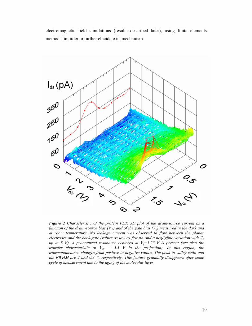
The 3D plot of the drain-source current as a function of the drain-source bias (Vds)
and of the gate bias (Vg) is displayed in Fig. 2. The transfer characteristic exhibits a
pronounced resonance centered at Vg=1.25V. In this region, the transconductance
changes from positive to negative values. The peak to valley ratio and the FWHM are
2 and 0.3V, respectively. This feature gradually disappears, typically after some gate
sweeps (Fig. 3). Since the fluorescence experiments in high electric field indicate that
azurin still preserves its structure, we ascribe this effect to metallic contact damage,
induced by the high electric field [3]. The ageing of nanodevices is a general issue
[see also 4, 5] that must be accurately addressed and we have carried out
0 1 2 3 4 5 60
100
200
C
urre
nt (p
A)
Voltage (V)
Cu-Az - Vg= 0.0V Cu-Az - Vg= 1.2V Zn-Az - Vg= 0.0V Zn-Az - Vg= 1.2V Apo-Az - Vg= 0.0V Apo-Az - Vg= 1.2V Silanes Silanes+Buffer
Figure 1 Current-voltage characteristics of devices made with azurin variants for two different gate voltages (0 V and 1.2 V). As a general feature, devices based on Zn-Az or Apo-Az exhibited low current (around 50 pA) with no modulation effect as a function of Vg. These results support the interpretation that conduction in the proteins and modulation in the devices is due to the reversible redox reaction Cu2+ + e- Cu1+, which reconverts continuously the Cu(II) copper oxidized state into the Cu(I) reduced state in adjacent molecules. As a reference, responses are also shown of devices that were either simply silanised or silanised and incubated in buffer without protein.
19
electromagnetic field simulations (results described later), using finite elements
methods, in order to further elucidate its mechanism.
Figure 2 Characteristic of the protein FET. 3D plot of the drain-source current as afunction of the drain-source bias (Vds) and of the gate bias (Vg) measured in the dark andat room temperature. No leakage current was observed to flow between the planarelectrodes and the back-gate (values as low as few pA and a negligible variation with Vgup to 8 V). A pronounced resonance centered at Vg=1.25 V is present (see also thetransfer characteristic at Vds = 5.5 V in the projection). In this region, thetransconductance changes from positive to negative values. The peak to valley ratio andthe FWHM are 2 and 0.3 V, respectively. This feature gradually disappears after somecycle of measurement due to the aging of the molecular layer
20
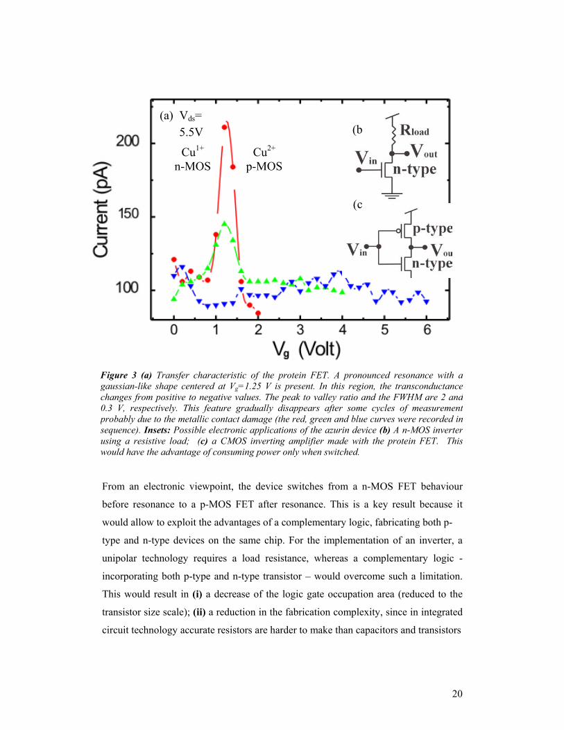
From an electronic viewpoint, the device switches from a n-MOS FET behaviour
before resonance to a p-MOS FET after resonance. This is a key result because it
would allow to exploit the advantages of a complementary logic, fabricating both p-
type and n-type devices on the same chip. For the implementation of an inverter, a
unipolar technology requires a load resistance, whereas a complementary logic -
incorporating both p-type and n-type transistor – would overcome such a limitation.
This would result in (i) a decrease of the logic gate occupation area (reduced to the
transistor size scale); (ii) a reduction in the fabrication complexity, since in integrated
circuit technology accurate resistors are harder to make than capacitors and transistors
(a) Vds= 5.5V
Cu1+ n-MOS
Cu2+
p-MOS
(b
(c
Figure 3 (a) Transfer characteristic of the protein FET. A pronounced resonance with agaussian-like shape centered at Vg=1.25 V is present. In this region, the transconductancechanges from positive to negative values. The peak to valley ratio and the FWHM are 2 and0.3 V, respectively. This feature gradually disappears after some cycles of measurementprobably due to the metallic contact damage (the red, green and blue curves were recorded insequence). Insets: Possible electronic applications of the azurin device (b) A n-MOS inverterusing a resistive load; (c) a CMOS inverting amplifier made with the protein FET. Thiswould have the advantage of consuming power only when switched.
21
and (iii) a reduction of power consumption because, as opposed to unipolar inverters
that consume power in the low state, CMOS consume power only when switching.
We ascribe these interesting results to the unique transport mechanism of our
biomolecular devices. Redox protein devices are very different from standard
inorganic semiconductors and conventional organic devices. Silicon MOSFETs and
thin-film transistor (TFTs) are based on a gate field modulating the width and the
conductance of a semiconducting channel, whereas a proposed mechanism for carbon
nanotube FETs is the Schottky-barrier dominated transport [6]. In proteins, the long-
range electron transfer (ET), which represents one of the key processes in
photosynthesis and respiration, occurs between a donor (D) and an acceptor (A) site.
Two different models for ET in proteins have been proposed [7], i.e. a superexchange
mechanism (consisting of direct quantum tunneling between the donor and acceptor)
and a sequential (incoherent) hopping between adjacent sites. The main factors
influencing the ET rate are: (1) the distance between the two redox centers (in
electron tunneling the ET rate decreases exponentially with distance, whereas in
hopping it is inversely related to the distance); (2) the nature of the micro-
environment separating the donor and the acceptor (which mediates the virtual state or
provides intermediate states, respectively), (3) the reorganization energy λ, i.e. the
energy required for all structural adjustments (in the reactants and in the surrounding
molecules) that are needed for the transfer of the electron [8] and (4) the driving force.
In particular, in the case of azurin, the essentially unchanged copper site geometry in
the Cu(II) and Cu(I) state minimizes the reorganization energy λ and favours fast
electron transfer.
The transport of electrons through systems containing redox sites (and thus in the Pro-
FET) occurs via electron hopping from one reduced (Cu(I)) molecule to an adjacent
oxidized (Cu(II)) molecule [9] (see inset of Fig. 4), which must behave as a redox
pair. For electrons to flow, therefore, both reduced and oxidized azurin must be
present and their relative proportion determines the ET rate. Let us introduce, in
analogy to solid-state physics, two functions 2Cuf + and 1Cuf + = 1 - 2Cuf + that
provide the probabilities that a copper site is in the Cu(I) and Cu(II) state, respectively
(i.e. the fraction of reduced and oxidized azurins in the layer). If Wim is the inter-
molecular transfer rate, the overall electron transfer rate WET takes the form:
22
WET(Vds,Vg) = Wim (Vds) 2Cuf + (Vg) 1Cuf + (Vg) = Wim 2Cuf + (Vg) (1- 2Cuf + (Vg))
where we have assumed that Vds and Vg influence Wim and 2Cuf + , respectively. In
other words, we propose that the inter-molecular transfer rate Wim depends on the in-
plane driving force, which is related to the bias applied between drain and source
electrodes (hopping mechanism). On the other hand, the azurin redox state is thought
to be regulated by Vg: thus, the higher Vg, the greater the fraction of oxidized azurins.
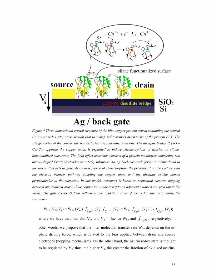
Figure 4 Three-dimensional crystal structure of the blue-copper protein azurin containing the central
Cu ion as redox site; cross-section (not to scale) and transport mechanism of the protein FET. The
site geometry of the copper site is a distorted trigonal bipyramid one. The disulfide bridge (Cys-3 –
Cys-26) opposite the copper atom, is exploited to induce chemisorptions of azurins on silane-
functionalized substrates. The field effect transistor consists of a protein monolayer connecting two
arrow-shaped Cr/Au electrodes on a SiO2 substrate. An Ag back-electrode forms an ohmic bond to
the silicon that acts as gate. As a consequence of chemisorption, the proteins sit on the surface with
the electron transfer pathway coupling the copper atom and the disulfide bridge almost
perpendicular to the substrate. In our model, transport is based on sequential electron hopping
between one reduced azurin (blue copper ion in the inset) to an adjacent oxidized one (red ion in the
inset). The gate (vertical) field influences the oxidation state of the redox site, originating the
resonance
23
This is reasonable since the protein is chemisorbed on the SiO2 surface with a known
ET route – joining the disulfide bridge to the copper site – almost perpendicular to the
surface. The probability that any two adjacent azurin molecules form a redox pair is
proportional to 2Cuf + (1- 2Cuf + ). This product is maximal when 1 – 2 2Cuf + = 0 or
2Cuf + = 0.5, i.e. when the two populations of azurin molecules are present in equal
amounts. At a particular value of Vg the fraction of oxidized molecule will equal that
of reduced molecules and therefore ET will be maximal. At higher (lower) Vg values,
the fraction of oxidized (reduced) molecules will be higher than that of reduced
(oxidized) molecules, resulting in a lower ET rate. This model explains the
phenomenon of resonance that we observe in the Pro-FET (Fig. 5) and opens the way
to a mathematical simulation of the device behaviour. Statistical considerations about
the equilibrium of the redox reaction involving the copper atom lead to a Fermi-like
functional dependence of 2Cuf + on Vg, where the midpoint potential (i.e. the voltage
at which the molecules are half oxidized and half reduced) is tuned by Vg, resulting in
a calculated probability for redox pair formation having a resonance-like shape. This
model is consistent with the interpretation of the redox peak in cyclic voltammetry
curves [10,11] and in electrochemical STM experiments [12] performed on azurins
chemisorbed on Au(111) substrates. To quantitatively simulate the device and to
identify the region involved in the ET process, Monte Carlo simulations based on this
model are currently in progress, taking into account the copper-mediated electron
transfer and the contribution from the intrinsic conductivity of the protein skeleton
(see section 3.4).
Comparison with devices based on mutant proteins The key role of the copper atom in electron transfer is further supported by a
comparison with the current-voltage curves measured in devices implemented with
two azurin variants: the first with the Cu atom replaced by a Zn atom (Zn-Az), the
second without metal atom (Apo-Az). In Fig.1, the I-V characteristics for two
different gate voltages (0 and 1.2 V, the latter corresponding to the resonance in the
transcharacteristics of the Cu-Az devices) are displayed for each protein device. The
current flowing through devices based on the two variants are significantly lower and
no modulation is observed between -6 and 6 volts. We ascribe the low conductivity of
these devices to the absence of a metal atom capable to mediate electron transfer,
24
since Apo-Az contains no metal atom, while Zn has only one oxidation state (Zn+2).
As a reference, the I-V characteristics of devices silanised or silanised and incubated
in buffer without protein are also reported in the same figure. In these cases the
currents are comparable with the noise level of empty devices.
Device aging and lifetime To complete the discussion, the issues of device ageing and lifetime have to be
addressed as a rule for molecular electronics, since the need for high throughput and
long-term stability is critical for transferring molecular electronics prototypes to
production. Device failure during operation can be accounted for by a degradation of
the molecular layer and/or a damage of nanojunctions. Even though our preliminary
data on protein fluorescence in an electric field demonstrate that the protein preserves
its structure under high fields, such fields usually lead to a damage of nanojunctions.
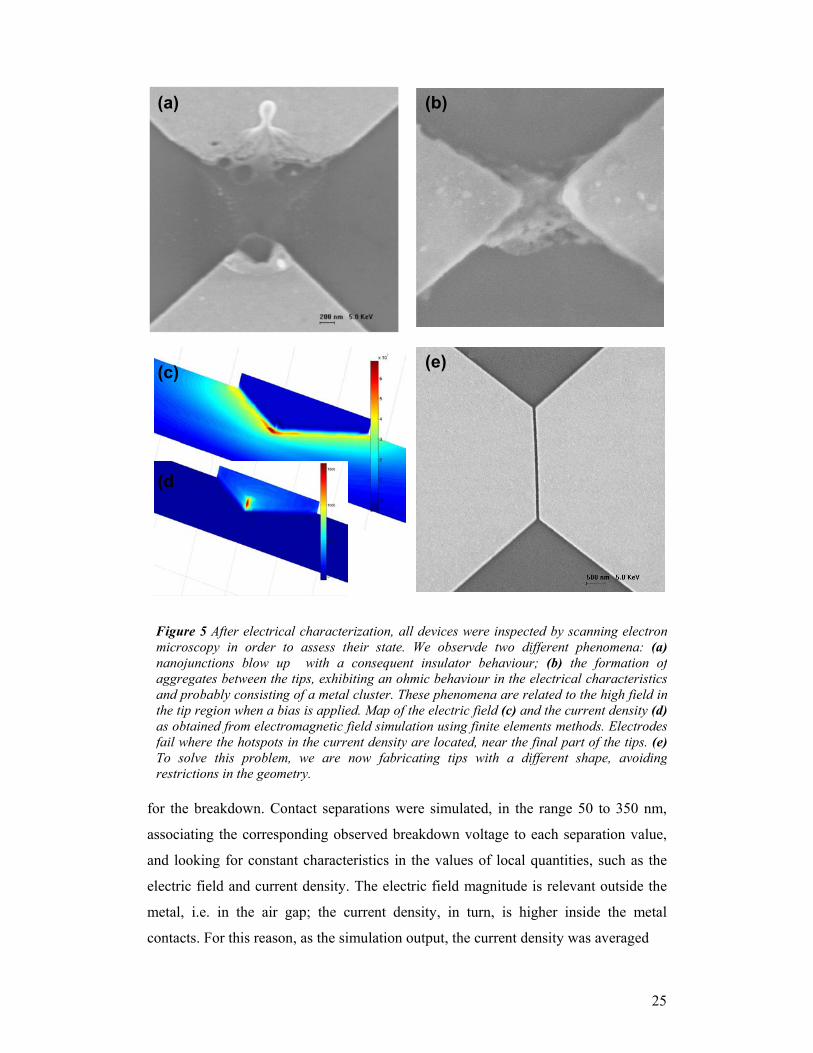
We observe two main phenomena concerning device damage: (1) blowing up of
nanojunctions (Figure 5a) or (2) the formation of various aggregates on the contacts
(Figure 5b). When we apply a bias, a very high electric field arises between the
electrodes (Figure 5c), because they are placed few tens of nanometers apart and there
is a drastic change in the dielectric constant at the interface between SiO2 and the
metal. This very intense electric field causes device damage.
A relationship was found between the contact separation and breakdown voltage,
(Fig. 6). The linear regression, with a slope of 1.1·105 V·cm-1, seems a valid model,
as expected for field-related phenomena, except that no intersection is predicted with
the origin. Furthermore, some devices were tested with azurin molecules in the gap,
some others without, and the presence of proteins was found to favour breakdown,
with a 50 % occurrence versus the 20 % of molecule-free devices. Finite elements
simulations were performed in order to investigate whether the breakdown could be
caused by the electric field or the current density (thermal effects can be excluded,
due to the characteristics of the phenomenon and the involved orders of magnitude).
The simulated geometry was pruned, with respect to the physical one, at a length of
few hundreds nanometers along the x-axis (joining the two tips). The silicon substrate,
underneath the SiO2 layer, was also reduced in thickness, due to the limited
penetration depth of current inside it. Dirichlet boundary conditions of fixed potential
were imposed on the outer borders of the tips, while Neumann conditions were set
anywhere else. No molecules were simulated, in this first model, in order to keep it as
general as possible; on the other hand, as mentioned, their presence is not necessary
25
for the breakdown. Contact separations were simulated, in the range 50 to 350 nm,
associating the corresponding observed breakdown voltage to each separation value,
and looking for constant characteristics in the values of local quantities, such as the
electric field and current density. The electric field magnitude is relevant outside the
metal, i.e. in the air gap; the current density, in turn, is higher inside the metal
contacts. For this reason, as the simulation output, the current density was averaged
(a) (b)
(c)
(d
(e)
Figure 5 After electrical characterization, all devices were inspected by scanning electronmicroscopy in order to assess their state. We observde two different phenomena: (a)nanojunctions blow up with a consequent insulator behaviour; (b) the formation ofaggregates between the tips, exhibiting an ohmic behaviour in the electrical characteristicsand probably consisting of a metal cluster. These phenomena are related to the high field inthe tip region when a bias is applied. Map of the electric field (c) and the current density (d)as obtained from electromagnetic field simulation using finite elements methods. Electrodesfail where the hotspots in the current density are located, near the final part of the tips. (e)To solve this problem, we are now fabricating tips with a different shape, avoidingrestrictions in the geometry.
26
over its hot-spot (the high-intensity area, containing the highest quartile as to the field
intensity distribution, inside the metal and close to the tip) as well as over the whole
tip, while the electric field was averaged over its own hot-spot, immediately outside
the metal tip. Due to the shape of the tips, that is the only place where a strong
interaction may take place between the field and the metal; consequently, there is no
point at taking the average electric field over the whole air gap.
Figs. 7 and 8 report these three quantities versus the contact separation: both the
electric field and current density, averaged over their respective hot-spots, decrease in
similar, nonlinear fashions, as the separation increases. The reason is the shape of the
field distribution: as the contacts get farther, the shape of the field and current density
near each tip tends to become more and more independent of the presence of the other
tip. The ‘knee’ between the more coupled and less coupled zone seems to be around
100 nm. Conversely, the average current density over the whole tip has a much more
constant trend; the calculated standard deviation is only 13.8%, versus more than 30%
found for the former quantities. In other words, the phenomenon seems to be
controlled by current density, and to need a minimum area of sufficiently
Figure 6 Empirical dependence between the activation voltage and contact separation, showing a linear regression
27
Figure 7 Average ‘hot-spot’ field, obtained by the simulations: for large separations, it tends toa constant value, confirming the linear relationship between voltage and separation, while withvery close tips the dependence becomes highly nonlinear
Figure 8 Average current density on the hot-spot (triangles) and over the whole tip (asterisks), as obtained by the simulations; the former behaves like the electric field, while the seconds is nearly constant
28
high density to be triggered; a small, though intensive hot-spot, is not enough.
Moreover, the ‘threshold’ values are reached just by applying the observed
breakdown voltages to the corresponding separation amplitudes. One can then extend
the breakdown law to smaller contact separations, just by finding what voltage must
be applied to any imposed gap, in order to obtain the needed average current density.
Fig. 9 shows the result of such procedure: for smaller gaps, the law becomes
definitely nonlinear, with the breakdown voltage decreasing more and more quickly
as the gap decreases: this phenomenon is due to the increasingly strong coupling
between the contacts, as already remarked, and shows that the apparently lack of
intersection with the origin is not real. On the other hand, for separations larger than
100 nm, the law tends to linearity, accounting for the behaviour observed in the
experimental data.
If breakdown has found a phenomenological description, much remains to be clarified
about its very nature. Electromigration is to be ruled out, at least in the form we know,
for the current is orders of magnitude lower than it usually is in this phenomenon. On
the other side, metal is clearly taken away from the contacts, and possible field-related
Figure 9 Activation law, as predicted from the simulations: the regime, linear for large separations, switches to nonlinear around 100 nm
29
explanations (e.g. field emission) contrast with the given description. Finally, the role
of azurin is still unclear: its capability of favouring breakdown might be attributed to
the increased conductivity of the inter-tip air channel – the same at the basis of protein
devices – but this is still to be ascertained and clarified in its dynamics. However, we
emphasize that the tip-geometry, though useful to realize very close electrodes,
introduces critical breaking points, related to the regions where the electric field is
higher (tips). An improvement can be obtained if discontinuities in the electrode
geometry are avoided to prevent field-induced damage. In order to reduce these
problems, we have started to fabricate electrodes with a trapezoidal shape (Figure 5d).
Moreover, we also fabricate more complex circuits (Figure 10) in order to study the
conductivity of several molecular devices in parallel. Since most of the designs and
prototypes for molecular electronics circuits and devices involve an interface between
a molecule and metal electrodes, the effects described must be carefully addressed
before molecular electronics can become of practical applicability.
3.2.2b Investigation of the structural stability of azurin monolayers in air
for device implementation We have shown that the azurin ET activity can be exploited for the realization of solid
state biomolecular transistors working in air and at room temperature. On the
biochemical and biophysical side, an important question is whether the protein
structure and function are conserved under non-physiological conditions. This is a key
technological point for the realization of such biodevices, but it is also an important
Figure 10 Nanojunctions for the study of the conductivity of several molecular devices in parallel.
30
issue from a fundamental viewpoint. In the Second Year Report, we provided a
complete and direct analysis of this issue, showing that the immobilization of azurin
in the solid state under non liquid conditions, by means of a specific chemisorption
process, does not result in protein denaturation. To this purpose, we carried out a
systematic investigation on the azurin monolayers, concluding that the immobilized
proteins do not undergo denaturation even after removal of the aqueous solvent. In
this Report, we show additional biophysical characterization of the protein
monolayers, demonstrating the possibility of inducing resonant tunnelling in azurin
even under ambient condition (thus demonstrating the retention of the proper ET
functionality of azurin molecules in air), and carefully testing the biomolecular films
in device-like conditions, namely (i) under high external electric fields and (ii) under
prolonged exposure to ambient conditions (ageing effects), which are crucial issues
for the reliability of protein-based devices.
ET functionality of azurin molecules under ambient conditions
The main focus of our study was to ascertain if immobilized azurin preserves its
electron transfer properties, especially in ambient conditions. STM permits to achieve
a very high resolution and to probe the electronic properties of analyte biomolecules,
providing crucial information on the integrity of the copper active site, and, hence, on
the functional state of the protein. STM experiments were carried out, both in buffer
solution and in air, on Cu azurin molecules covalently immobilized onto Au(111)
substrates via the disulphide bridge Cys3-Cys26.
Au(111) grown on muscovite mica sheets (Molecular Imaging) were flame-
annealed to obtain recrystallized terraces and immediately incubated in 70µM azurin
(50mM sodium acetate, pH 4.6) at 4°C for 1.5 h. After incubation, the samples were
gently rinsed with ultrapure water, dried with a soft jet of pure nitrogen, and
immediately imaged by STM in buffer solution or in air.
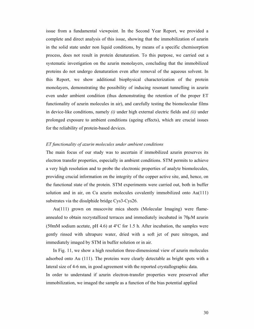
In Fig. 11, we show a high resolution three-dimensional view of azurin molecules
adsorbed onto Au (111). The proteins were clearly detectable as bright spots with a
lateral size of 4-6 nm, in good agreement with the reported crystallographic data.
In order to understand if azurin electron-transfer properties were preserved after
immobilization, we imaged the sample as a function of the bias potential applied
31
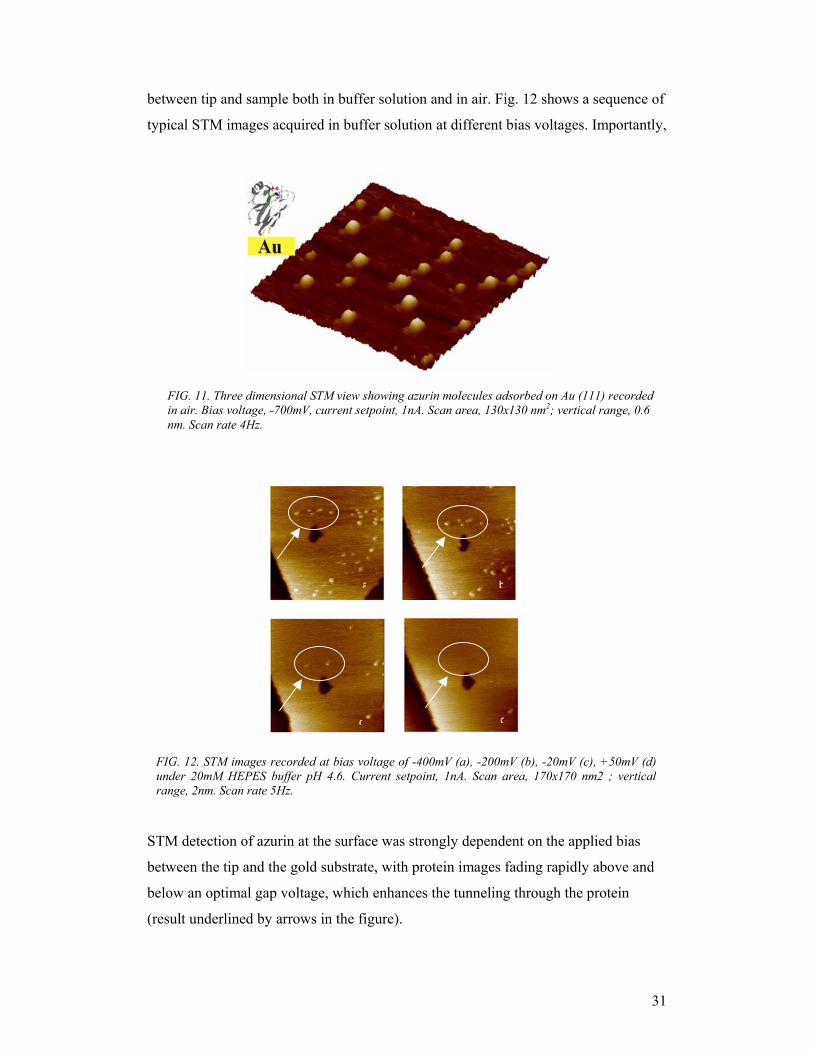
between tip and sample both in buffer solution and in air. Fig. 12 shows a sequence of
typical STM images acquired in buffer solution at different bias voltages. Importantly,
STM detection of azurin at the surface was strongly dependent on the applied bias
between the tip and the gold substrate, with protein images fading rapidly above and
below an optimal gap voltage, which enhances the tunneling through the protein
(result underlined by arrows in the figure).
FIG. 11. Three dimensional STM view showing azurin molecules adsorbed on Au (111) recorded in air. Bias voltage, -700mV, current setpoint, 1nA. Scan area, 130x130 nm2; vertical range, 0.6 nm. Scan rate 4Hz.
a b
c d
FIG. 12. STM images recorded at bias voltage of -400mV (a), -200mV (b), -20mV (c), +50mV (d)under 20mM HEPES buffer pH 4.6. Current setpoint, 1nA. Scan area, 170x170 nm2 ; verticalrange, 2nm. Scan rate 5Hz.
32
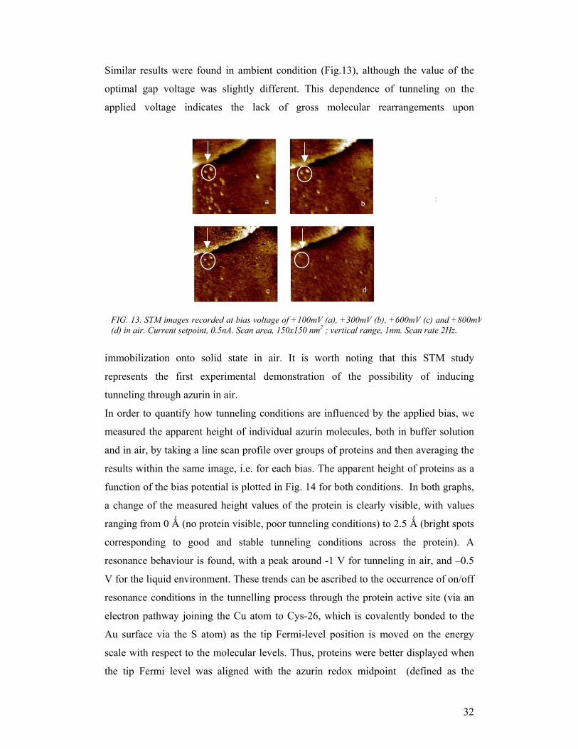
Similar results were found in ambient condition (Fig.13), although the value of the
optimal gap voltage was slightly different. This dependence of tunneling on the
applied voltage indicates the lack of gross molecular rearrangements upon
immobilization onto solid state in air. It is worth noting that this STM study
represents the first experimental demonstration of the possibility of inducing
tunneling through azurin in air.
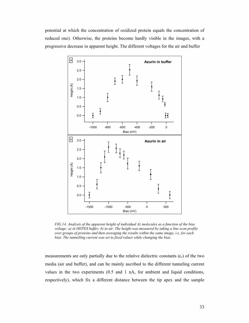
In order to quantify how tunneling conditions are influenced by the applied bias, we
measured the apparent height of individual azurin molecules, both in buffer solution
and in air, by taking a line scan profile over groups of proteins and then averaging the
results within the same image, i.e. for each bias. The apparent height of proteins as a
function of the bias potential is plotted in Fig. 14 for both conditions. In both graphs,
a change of the measured height values of the protein is clearly visible, with values
ranging from 0 Ǻ (no protein visible, poor tunneling conditions) to 2.5 Ǻ (bright spots
corresponding to good and stable tunneling conditions across the protein). A
resonance behaviour is found, with a peak around -1 V for tunneling in air, and –0.5
V for the liquid environment. These trends can be ascribed to the occurrence of on/off
resonance conditions in the tunnelling process through the protein active site (via an
electron pathway joining the Cu atom to Cys-26, which is covalently bonded to the
Au surface via the S atom) as the tip Fermi-level position is moved on the energy
scale with respect to the molecular levels. Thus, proteins were better displayed when
the tip Fermi level was aligned with the azurin redox midpoint (defined as the
a b
c d
FIG. 13. STM images recorded at bias voltage of +100mV (a), +300mV (b), +600mV (c) and +800mV(d) in air. Current setpoint, 0.5nA. Scan area, 150x150 nm2 ; vertical range, 1nm. Scan rate 2Hz.
33
potential at which the concentration of oxidized protein equals the concentration of
reduced one). Otherwise, the proteins become hardly visible in the images, with a
progressive decrease in apparent height. The different voltages for the air and buffer
measurements are only partially due to the relative dielectric constants (εr) of the two
media (air and buffer), and can be mainly ascribed to the different tunneling current
values in the two experiments (0.5 and 1 nA, for ambient and liquid conditions,
respectively), which fix a different distance between the tip apex and the sample
3.0
2.5
2.0
1.5
1.0
0.5
0.0
Hei
ght (
Å)
-1000 -800 -600 -400 -200 0Bias (mV)
Azurin in buffer
3.0
2.5
2.0
1.5
1.0
0.5
0.0
Hei
ght (
Å)
-1500 -1000 -500 0 500Bias (mV)
Azurin in air
a
b
FIG.14. Analysis of the apparent height of individual Az molecules as a function of the bias voltage: a) in HEPES buffer; b) in air. The height was measured by taking a line scan profile over groups of proteins and then averaging the results within the same image, i.e. for each bias. The tunnelling current was set to fixed values while changing the bias.
34
surface. By increasing the current, the tip is closer to the sample and the electrostatic
field felt by the protein is larger. This experimental evidence suggests that the charge
distribution on the protein surface remains the same both in air and in a liquid
environment (likely due to the retention of the hydration shells) indicating structural
robustness of the protein in both cases. These results are in agreement with similar
experiments performed by in situ EC-STM on gold-adsorbed azurins, in which (using
a bipotentiostatic control) the substrate potential was changed with respect to a
reference electrode, while the tip-sample bias was held constant.
In conclusion, we have demonstrated for the first time the possibility of inducing a
tunneling current through azurin in air. Moreover, we have demonstrated that
chemisorption of azurin in the solid state does not alter its conformation and the redox
site structure even after the removal of the aqueous solvent, and is therefore likely to
preserve its ET function(s). Such an important result discloses very interesting
perspectives for the development of hybrid nanodevices operating in non-liquid
environments.
Azurin for biomolecular electronics: a reliability study
In this section data are presented on the resilience of the metalloprotein azurin to high
electric fields and ambient conditions, which are crucial issues for the reliability of
azurin-based devices. Concerning the effect of electric fields, two models are
discussed, which agree in indicating an unexpectedly high robustness. The predictions
were confirmed by experiments in device-like conditions: no structural modifications
occur even after a 40-minute exposure to tens of MV/m. Ageing was then investigated
experimentally, at ambient conditions and without field, over several days. Only a
small conformational rearrangement was observed over the first ten hours, followed
by an equilibrium state.
i) Conformational properties of azurin in high external electric fields As shown in this report, the metalloprotein azurin can been successfully employed in
rectifying (diode-like) and modulating (transistor-like) biomolecular devices, its key
properties being the capability of exchanging electrons through its active site, via
redox reactions. Yet, two major objections are frequently raised against electronic
application of biomolecules. First, the high electric fields applied in nanometric
devices (in the order of 107 V/m) are often indicated as potential sources of rapid
35
molecular degradation. Secondarily, the structural stability of biological
macromolecules to ambient conditions (in air) is critical, and potentially affects the
durability of devices. In this study, the reliability of azurin-based devices is
investigated in both respects.
An estimate of the inner electric fields in azurin was derived by Car-Parrinello
calculation of the potential (performed by the INFM-Modena Group). The field was
then calculated as the spatial gradient of the potential, on the same computational
grid.
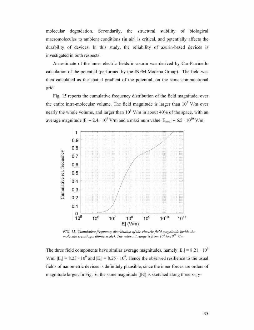
Fig. 15 reports the cumulative frequency distribution of the field magnitude, over
the entire intra-molecular volume. The field magnitude is larger than 107 V/m over
nearly the whole volume, and larger than 108 V/m in about 40% of the space, with an
average magnitude |E| = 2.4 · 109 V/m and a maximum value |Emax| = 6.5 · 1010 V/m.
The three field components have similar average magnitudes, namely |Ex| = 8.21 · 109
V/m, |Ey| = 8.23 · 109 and |Ez| = 8.25 · 109. Hence the observed resilience to the usual
fields of nanometric devices is definitely plausible, since the inner forces are orders of
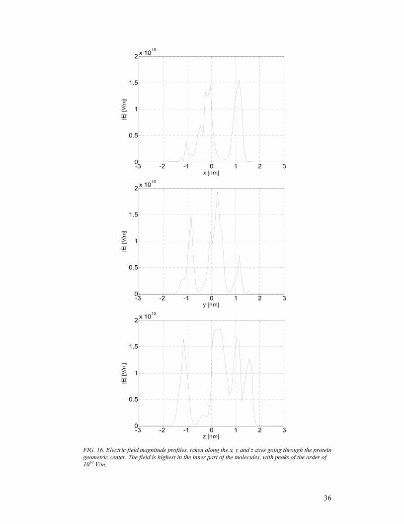
magnitude larger. In Fig.16, the same magnitude (|E|) is sketched along three x-, y-
FIG. 15: Cumulative frequency distribution of the electric field magnitude inside the molecule (semilogarithmic scale). The relevant range is from 106 to 1010 V/m.
|E| (V/m)1010
0.1
0.2
0.3
0.4
0.5
0.6
0.7
0.8 0.9
1
10 5 10 6 107 108 109 10 11 0
Cum
ulat
ive
rel.
freq
uenc
y
36
-3 -2 -1 0 1 2 30
0.5
1
1.5
2 x 10¹⁰
x [nm]
|E| [
V/m
]
-3 -2 -1 0 1 2 30
0.5
1
1.5
2 x 10¹⁰
y [nm]
|E| [
V/m
]
-3 -2 -1 0 1 2 30
0.5
1
1.5
2 x 10¹⁰
z [nm]
|E| [
V/m
]
FIG. 16. Electric field magnitude profiles, taken along the x, y and z axes going through the protein geometric center. The field is highest in the inner part of the molecules, with peaks of the order of 1010 V/m.
37
and z-parallel axes, intersecting in the geometric center of the protein; the portion of
each axis falling inside the inner volume of azurin is between -2 and 2 nm.
The same qualitative conclusions can be reached by resorting to a much simpler
analytical model, based on the approximate global geometry of azurin and its strong
dipole (≈150 D). In particular, approximating the globular-shaped azurin to a sphere,
with uniform polarization p, a well-known result of electrostatics states that the
magnitude of the inner (uniform) electric field is:
03εpE =
where ε0 is the permittivity of vacuum. p, integrated over the volume, must yield the
known dipole moment P; hence:
30
3 4)3/4( RPE
RPp
εππ=⇒=
where R is the radius of the sphere; assuming R = 2 nm, one obtains |E| = 2.8 · 108
V/m. This value, lower than that from Car-Parrinello by one order of magnitude, is
explained by the uniform orientation of the field: in this simplified model the field
sums up concordantly throughout the volume, to give the total dipole moment. In
contrast, the true field components have variable orientation; as a proof, one can
determine their algebraic average value from the Car-Parrinello calculation: Ex = -3.3
· 106 V/m, Ey = -3.3 · 106 V/m and Ez = -2.4 · 106 V/m, which is two orders of
magnitude lower than the average magnitude calculated above. For this reason, the
analytical model is conservative; this is probably the general case, with uniform-field
approximations. The dipole moment of azurin has been determined theoretically;
however, when the geometry and dipole are experimentally known, a simple model
like the one presented here may be useful for gross evaluation of molecular resilience,
avoiding cumbersome theoretical calculations.
The theoretical predictions agree in indicating that the effect of device-level electric
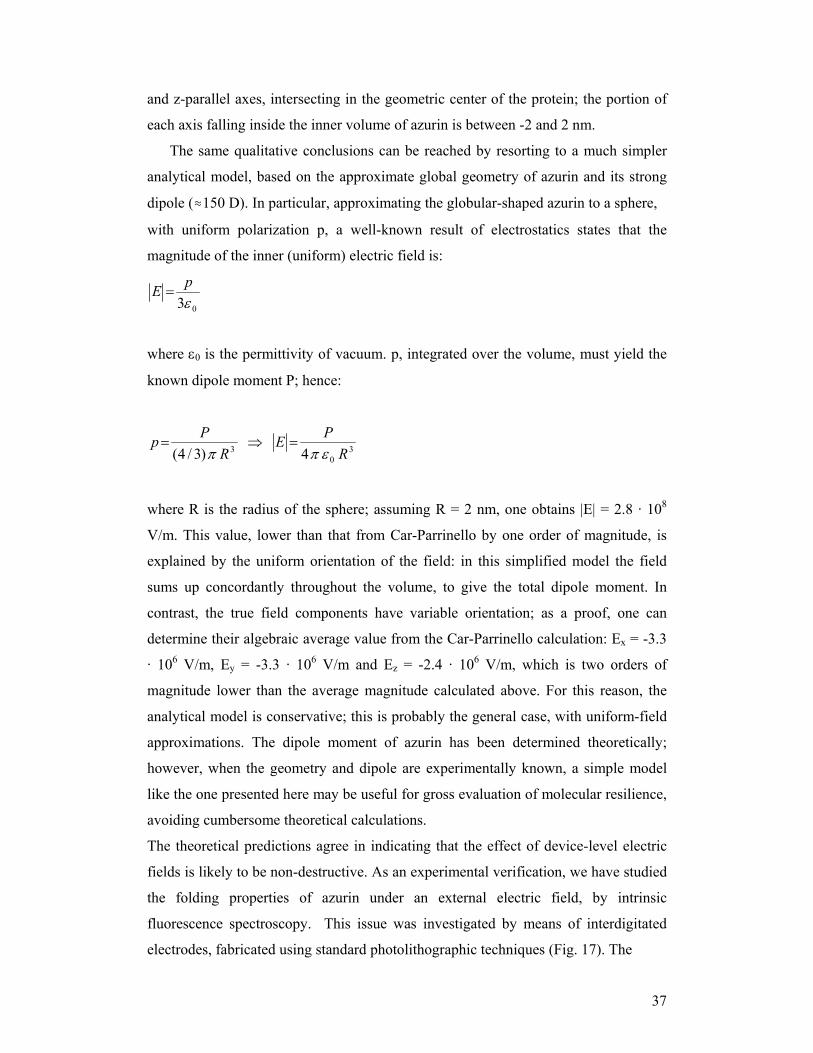
fields is likely to be non-destructive. As an experimental verification, we have studied
the folding properties of azurin under an external electric field, by intrinsic
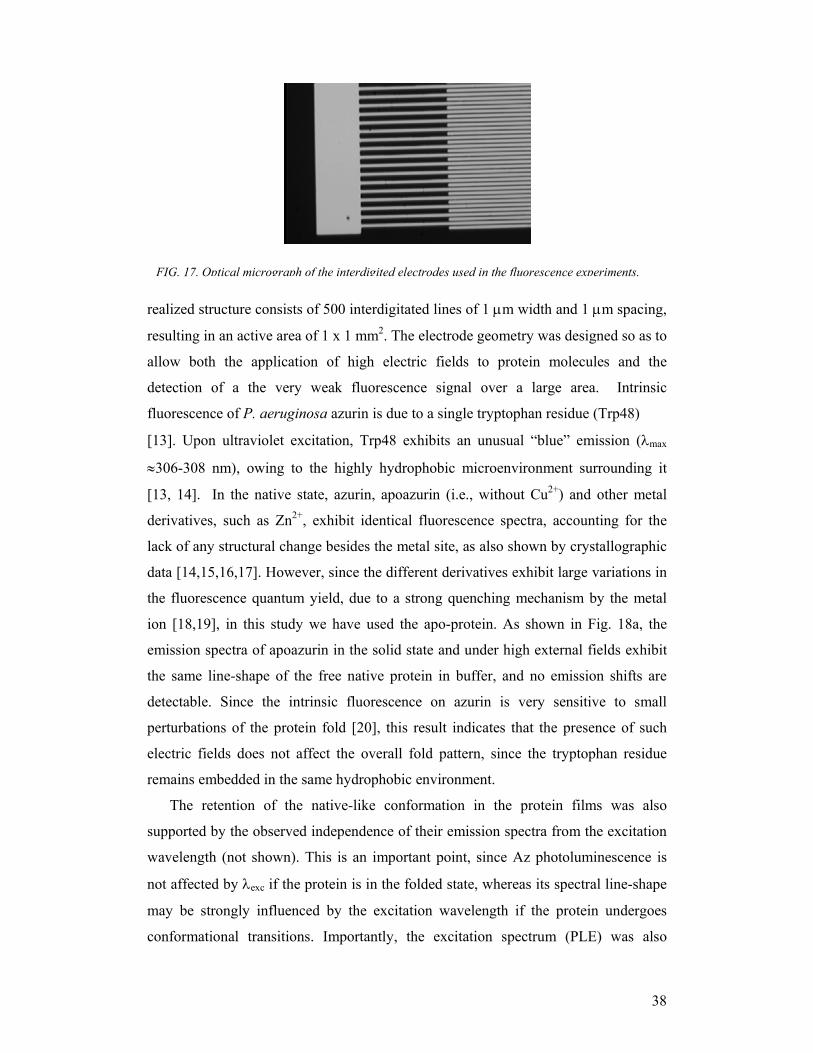
fluorescence spectroscopy. This issue was investigated by means of interdigitated
electrodes, fabricated using standard photolithographic techniques (Fig. 17). The
38
realized structure consists of 500 interdigitated lines of 1 µm width and 1 µm spacing,
resulting in an active area of 1 x 1 mm2. The electrode geometry was designed so as to
allow both the application of high electric fields to protein molecules and the
detection of a the very weak fluorescence signal over a large area. Intrinsic
fluorescence of P. aeruginosa azurin is due to a single tryptophan residue (Trp48)
[13]. Upon ultraviolet excitation, Trp48 exhibits an unusual “blue” emission (λmax
≈306-308 nm), owing to the highly hydrophobic microenvironment surrounding it
[13, 14]. In the native state, azurin, apoazurin (i.e., without Cu2+) and other metal
derivatives, such as Zn2+, exhibit identical fluorescence spectra, accounting for the
lack of any structural change besides the metal site, as also shown by crystallographic
data [14,15,16,17]. However, since the different derivatives exhibit large variations in
the fluorescence quantum yield, due to a strong quenching mechanism by the metal
ion [18,19], in this study we have used the apo-protein. As shown in Fig. 18a, the
emission spectra of apoazurin in the solid state and under high external fields exhibit
the same line-shape of the free native protein in buffer, and no emission shifts are
detectable. Since the intrinsic fluorescence on azurin is very sensitive to small
perturbations of the protein fold [20], this result indicates that the presence of such
electric fields does not affect the overall fold pattern, since the tryptophan residue
remains embedded in the same hydrophobic environment.
The retention of the native-like conformation in the protein films was also
supported by the observed independence of their emission spectra from the excitation
wavelength (not shown). This is an important point, since Az photoluminescence is
not affected by λexc if the protein is in the folded state, whereas its spectral line-shape
may be strongly influenced by the excitation wavelength if the protein undergoes
conformational transitions. Importantly, the excitation spectrum (PLE) was also
FIG. 17. Optical micrograph of the interdigited electrodes used in the fluorescence experiments.
39
unchanged upon electric field application (Fig. 18b), thus demonstrating the absence
of any relevant perturbation in the physico-chemical conditions of the chromophore
microenvironment, and confirming that such field intensities do not interfere with the
conformation of the native protein. Moreover, it is interesting to note the clear
retention of structured luminescence spectra (both PL and PLE) by solid state films,
which are peculiar features of the native Az conformation (in its native state, Trp48 is
shielded in the rigid and highly hydrophobic core of the protein). This specifically
contrasts with typical broadband, red-shifted emissions of unfolded azurins, which are
completely devoid of any spectral structure.
In the case of azurin, the investigation of the microenvironment surrounding
Trp48 is of particular relevance, since this residue is thought to play an important role
in the long-range ET processes through the molecule [13; 21]. In addition, this results
is important also because it was obtained with the apo derivative, which is
characterized by a lower structural stability with respect to the wild type copper
protein [20]. Hence, our data indicate the lack of gross molecular rearrangements even
under these extreme experimental conditions.
Although the protein inner field intensities calculated above (up to 1010 V/m) may
sound unrealistic, our values are in very close agreement with recent studies [22,23],
in which the intriguing result that the density of the first hydration shell is higher than
that of bulk water [24] was theoretically elucidated in terms of “electrostriction” of
the water molecules by the huge electric field values (~109 V/m) at the surface of the
biomolecules. In addition, molecular dynamics simulations by Xu et al. on trypsin
inhibitor [25] have demonstrated that field strengths in the range of 108 V/m do not
alter the overall structure (or temperature) of the protein (such fields are shown to be
within thermal fluctuations), and only fields higher than 109 V/m can induce
significant structural changes [25]. All these considerations agree with our
experiments in indicating that the conformational state of the protein was not
significantly perturbed with respect to the native state upon external field application.
In conclusion, the available evidence suggests that: i) proteins in the solid state are
capable of maintaining the tightly bound hydration shells and a native-like
conformation, even after solvent removal and application of high external fields; ii)
this conclusion may appear less surprising if the huge intensity of the protein inner
fields is taken into account.
40
ii) Aging effects on azurin films in air
To investigate the second reliability issue (ageing of azurin in air, at ambient
conditions), experiments were performed in a similar fashion to the previous section
except that no electric field was applied. Experimental evidence has already been
presented that immobilization of azurin in a solid state monolayer in air does not
necessarily lead to protein denaturation (see Second Year Report and [26]). Now the
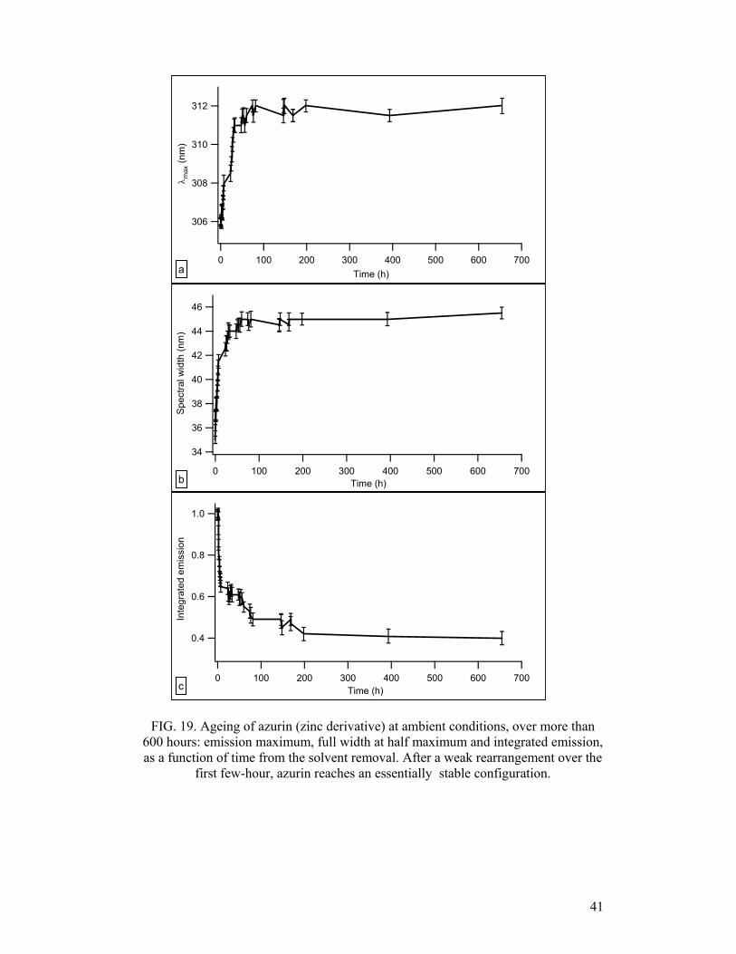
ageing of azurin was monitored over periods longer than 600 hours. Fig. 19 reports
the emission maximum (λmax), full width at half maximum (FWHM) and integrated
emission, all as a function of time, from the solvent removal instant: as seen, solid
state proteins undergo some conformational rearrangement. Such rearrangement is
however of modest entity: (Fig. 19a), since there is only a slight red-shift of azurin
PL, which brings λmax to a maximum of 311÷312 nm, well beneath the typical
broadband “red” emission of denatured azurin (λmax ≈ 355 nm). Most of this
modification takes place within the first 7 hours: during this period, a small
conformational transition is observed, after which a further slight rearrangement
slowly takes place within the first 100 hours. This behaviour emerges from all three
spectral parameters, which exhibit very close agreement. Remarkably, no other
significant conformational change is observed past the first 100 hours, suggesting that
the proteins do not experience denaturation even after weeks under non-physiological
conditions. It seems that proteins at ambient conditions (room temperature, 50÷60%
relative humidity) reach an equilibrium state, in which the new conformational pattern
is unperturbed. Such stability may be attributed to the capability of proteins to retain
their hydration shells, even under these experimental conditions. It is worth noting
that upon rehydration at the end of the test proteins return to exhibit a native-like
conformation, since their PL spectrum is typical of properly folded azurin. In
conclusion azurin proves to be a much more reliable material than it might have been
argued based upon some qualitative remarks. These results should go some way
towards dispelling the scepticism surrounding the use of proteins for biomolecular
devices
41
1.0
0.8
0.6
0.4
Inte
grat
ed e
mis
sion
7006005004003002001000Time (h)
46
44
42
40
38
36
34
Spe
ctra
l wid
th (n
m)
7006005004003002001000Time (h)
312
310
308
306
λ max
(nm
)
7006005004003002001000Time (h)a
b
c
FIG. 19. Ageing of azurin (zinc derivative) at ambient conditions, over more than 600 hours: emission maximum, full width at half maximum and integrated emission, as a function of time from the solvent removal. After a weak rearrangement over the
first few-hour, azurin reaches an essentially stable configuration.
42
3.2.2 Completion of M7 : Sub-10 nm gate for single molecule trapping and transport through the single molecule (INFM-Lecce)
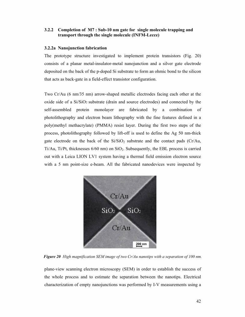
3.2.2a Nanojunction fabrication
The prototype structure investigated to implement protein transistors (Fig. 20)
consists of a planar metal-insulator-metal nanojunction and a silver gate electrode
deposited on the back of the p-doped Si substrate to form an ohmic bond to the silicon
that acts as back-gate in a field-effect transistor configuration.
Two Cr/Au (6 nm/35 nm) arrow-shaped metallic electrodes facing each other at the
oxide side of a Si/SiO2 substrate (drain and source electrodes) and connected by the
self-assembled protein monolayer are fabricated by a combination of
photolithography and electron beam lithography with the fine features defined in a
poly(methyl methacrylate) (PMMA) resist layer. During the first two steps of the
process, photolithography followed by lift-off is used to define the Ag 50 nm-thick
gate electrode on the back of the Si/SiO2 substrate and the contact pads (Cr/Au,
Ti/Au, Ti/Pt, thicknesses 6/60 nm) on SiO2. Subsequently, the EBL process is carried
out with a Leica LION LV1 system having a thermal field emission electron source
with a 5 nm point-size e-beam. All the fabricated nanodevices were inspected by
plane-view scanning electron microscopy (SEM) in order to establish the success of
the whole process and to estimate the separation between the nanotips. Electrical
characterization of empty nanojunctions was performed by I-V measurements using a
Figure 20 High magnification SEM image of two Cr/Au nanotips with a separation of 100 nm.
43
semiconductor parameter analyzer. Typically, about 90% of nanojunctions were of
good quality with no-leakage and open-circuit resistance higher than 1 TΩ. Using this
standard EBL process, we obtain inter-electrodes separation not smaller than 30-40
nm. The final electrode distance reflects exactly the design. Note that the progressive
reduction of the electrode width approaching the nanojunction - in a tip-like geometry
- is useful in order to reach very small inter-electrode distances, since it facilitates the
lift-off process.
If necessary, the inter-electrode separation is reduced down to few nanometers (for
single molecule trapping) using two different techniques: a brushing method [3] or by
means of an additional process consisting of Au electrodeposition [27]. The first
method consists in a partial exposure of the resist before the standard EBL process, by
brushing the PMMA layer for a precise short time, in the range of few seconds, with a
defocused electron-beam. In Figure 21a, the reduction of tip separation as a function
of the brushing time is shown. By a careful calibration of the brushing time between
10 and 60 s, the inter-electrode distance is reduced almost linearly from 50 nm down
to 10 nm; for t >60 s, the tip separation goes to zero. The inset of Figure 21a outlines
our exposure technique. Figure 21b shows a high magnification SEM image of Cr/Au
nanotips with separation of only 20 nm obtained by EBL with additional e-beam
brushing (t ≅ 40 s). Electrode distance could also be reduced by increasing the dose,
but in this case we lack a fine control of the process.
In the second approach, an additional Au electrodeposition step is performed by using
a commercial Au-cyanide electroplating set-up. High magnification (HM) SEM
images of nanojunctions fabricated by Au electrodeposition are reported in Fig. 22.
The calibration curve of the Au electrodeposition process (Fig.22a) shows the
reduction of the inter-electrode gap as a function of process duration, from an initial
value of 100 nm, to a resolvable minimum gap of only 7±2 nm (Fig.22e). The lateral
growth rate varies from 1.66 nm/s at the beginning to 2.5 nm/s when the gap is
reduced below 20 nm. Due to possible small instabilities of electrodeposition process
parameters (temperature and pH of the solution, resistance of the contacts, etc.) with
consequent changes of the Au lateral growth rate, the percentage yield for a
programmed sub-10nm gap is in the range 20-30%. To remove all PMMA residues
and contaminations between the planar electrodes, an O2 plasma treatment is carried
out at the end of the process. Both these methods to reduce the inter-electrode

44
separation have advantages and drawbacks. The brushing technique provides a higher
throughput while the Au electrodeposition allows to obtain closer electrodes, although
in this case contaminations between the planar electrodes reduce the process yield.
The calibration curve of the Au electrodeposition process (Fig.22a) shows the
reduction of the inter-electrode gap as a function of process duration, from an initial
value of 100 nm, to a resolvable minimum gap of only 7±2 nm (Fig.22e). The lateral
growth rate varies from 1.66 nm/s at the beginning to 2.5 nm/s when the gap is
reduced below 20 nm. Due to possible small instabilities of electrodeposition process
parameters (temperature and pH of the solution, resistance of the contacts, etc.) with
consequent changes of the Au lateral growth rate, the percentage yield for a
programmed sub-10nm gap is in the range 20-30%. To remove all PMMA residues
and contaminations between the planar electrodes, an O2 plasma treatment is carried
out at the end of the process. Both these methods to reduce the inter-electrode
separation have advantages and drawbacks. The brushing technique provides a higher
Figure 21 (a) Reduction of the separation between electrodes as a function of the brushing time (∆t) of the PMMA resist by a defocused e-beam. When ∆t ranges from 0 to 50 s, the tip separation is reduced almost linearly from 50 nm (the nominal one) to 10 nm; for ∆t= 60 s, the tip separation becomes zero. The insets outline our exposure technique. (i) Gaussian shape of the e-beam; (ii) The exposure overlap between two adjacent points. (iii) Our exposure strategy. First, the resist is partially exposed by means of a defocused e-beam (gray background in the inset, instead of the previous black one). Then, during the following EBL process, the Gaussian shape of the e-beam allows the resist near the edges of the tip to reach the right dose, resulting in a final electrode distance (d) inferior to the nominal exposure length (L). The evaluated deviation of d is of the order of 5 nm, due to process parameters such as the point-size of the beam, the step size of the exposure and the SEM resolution. (b) Plan-view SEM image of Cr-Au nanotips with a separation of 20 nm obtained with a brushing time of 40 s.
b) a)
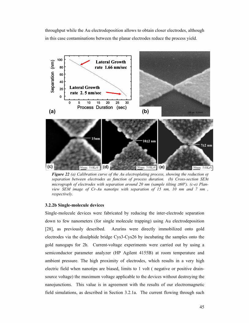
45
throughput while the Au electrodeposition allows to obtain closer electrodes, although
in this case contaminations between the planar electrodes reduce the process yield.
3.2.2b Single-molecule devices
Single-molecule devices were fabricated by reducing the inter-electrode separation
down to few nanometers (for single molecule trapping) using Au electrodeposition
[28], as previously described. Azurins were directly immobilized onto gold
electrodes via the disulphide bridge Cys3-Cys26 by incubating the samples onto the
gold nanogaps for 2h. Current-voltage experiments were carried out by using a
semiconductor parameter analyzer (HP Agilent 4155B) at room temperature and
ambient pressure. The high proximity of electrodes, which results in a very high
electric field when nanotips are biased, limits to 1 volt ( negative or positive drain-
source voltage) the maximum voltage applicable to the devices without destroying the
nanojunctions. This value is in agreement with the results of our electromagnetic
field simulations, as described in Section 3.2.1a. The current flowing through such
100n
0 5 10 15 20 25 30
0
20
40
60
80
100
Sepa
ratio
n(n
m)
Process Duration (sec)
Lateral Growthrate 1.66 nm/sec
Lateral Growthrate 2. 5 nm/sec
0 5 10 15 20 25 30
0
20
40
60
80
100
Sepa
ratio
n(n
m)
Process Duration (sec)
Lateral Growthrate 1.66 nm/sec
Lateral Growthrate 2. 5 nm/sec
0 5 10 15 20 25 30
0
20
40
60
80
100
Sepa
ratio
n(n
m)
Process Duration (sec)
Lateral Growthrate 1.66 nm/sec
Lateral Growthrate 2. 5 nm/sec
(b) (a)
Figure 22 (a) Calibration curve of the Au electroplating process, showing the reduction ofseparation between electrodes as function of process duration. (b) Cross-section SEMmicrograph of electrodes with separation around 20 nm (sample tilting ≅60°). (c-e) Plan-view SEM image of Cr-Au nanotips with separation of 15 nm, 10 nm and 7 nm ,respectively.
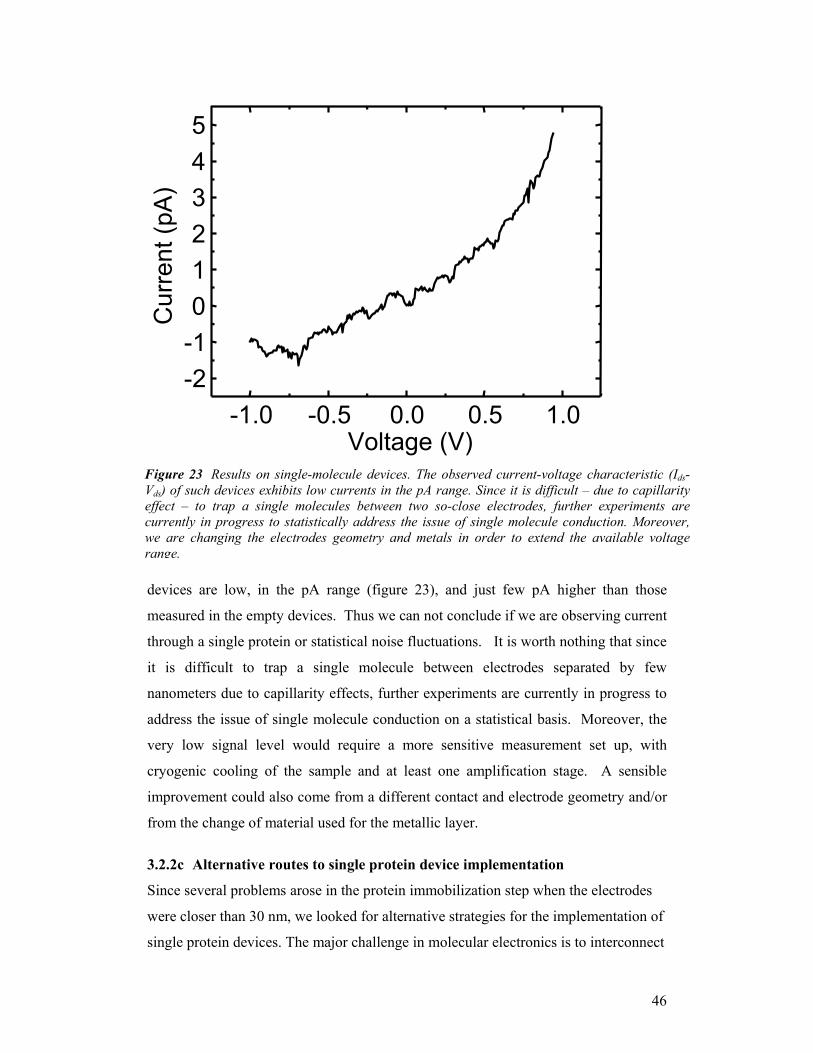
46
devices are low, in the pA range (figure 23), and just few pA higher than those
measured in the empty devices. Thus we can not conclude if we are observing current
through a single protein or statistical noise fluctuations. It is worth nothing that since
it is difficult to trap a single molecule between electrodes separated by few
nanometers due to capillarity effects, further experiments are currently in progress to
address the issue of single molecule conduction on a statistical basis. Moreover, the
very low signal level would require a more sensitive measurement set up, with
cryogenic cooling of the sample and at least one amplification stage. A sensible
improvement could also come from a different contact and electrode geometry and/or
from the change of material used for the metallic layer.
3.2.2c Alternative routes to single protein device implementation
Since several problems arose in the protein immobilization step when the electrodes
were closer than 30 nm, we looked for alternative strategies for the implementation of
single protein devices. The major challenge in molecular electronics is to interconnect
Figure 23 Results on single-molecule devices. The observed current-voltage characteristic (Ids-Vds) of such devices exhibits low currents in the pA range. Since it is difficult – due to capillarityeffect – to trap a single molecules between two so-close electrodes, further experiments arecurrently in progress to statistically address the issue of single molecule conduction. Moreover,we are changing the electrodes geometry and metals in order to extend the available voltagerange.
-1.0 -0.5 0.0 0.5 1.0 -2 -1 0 1 2 3 4 5
Cur
rent
(pA
)
Voltage (V)
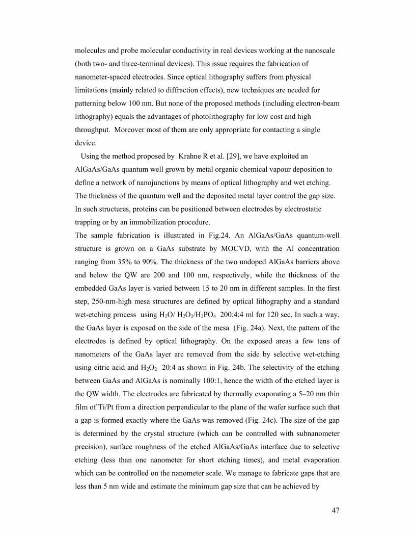
47
molecules and probe molecular conductivity in real devices working at the nanoscale
(both two- and three-terminal devices). This issue requires the fabrication of
nanometer-spaced electrodes. Since optical lithography suffers from physical
limitations (mainly related to diffraction effects), new techniques are needed for
patterning below 100 nm. But none of the proposed methods (including electron-beam
lithography) equals the advantages of photolithography for low cost and high
throughput. Moreover most of them are only appropriate for contacting a single
device.
Using the method proposed by Krahne R et al. [29], we have exploited an
AlGaAs/GaAs quantum well grown by metal organic chemical vapour deposition to
define a network of nanojunctions by means of optical lithography and wet etching.
The thickness of the quantum well and the deposited metal layer control the gap size.
In such structures, proteins can be positioned between electrodes by electrostatic
trapping or by an immobilization procedure.
The sample fabrication is illustrated in Fig.24. An AlGaAs/GaAs quantum-well
structure is grown on a GaAs substrate by MOCVD, with the Al concentration
ranging from 35% to 90%. The thickness of the two undoped AlGaAs barriers above
and below the QW are 200 and 100 nm, respectively, while the thickness of the
embedded GaAs layer is varied between 15 to 20 nm in different samples. In the first
step, 250-nm-high mesa structures are defined by optical lithography and a standard
wet-etching process using H2O/ H2O2/H2PO4 200:4:4 ml for 120 sec. In such a way,
the GaAs layer is exposed on the side of the mesa (Fig. 24a). Next, the pattern of the
electrodes is defined by optical lithography. On the exposed areas a few tens of
nanometers of the GaAs layer are removed from the side by selective wet-etching
using citric acid and H2O2 20:4 as shown in Fig. 24b. The selectivity of the etching
between GaAs and AlGaAs is nominally 100:1, hence the width of the etched layer is
the QW width. The electrodes are fabricated by thermally evaporating a 5–20 nm thin
film of Ti/Pt from a direction perpendicular to the plane of the wafer surface such that
a gap is formed exactly where the GaAs was removed (Fig. 24c). The size of the gap
is determined by the crystal structure (which can be controlled with subnanometer
precision), surface roughness of the etched AlGaAs/GaAs interface due to selective
etching (less than one nanometer for short etching times), and metal evaporation
which can be controlled on the nanometer scale. We manage to fabricate gaps that are
less than 5 nm wide and estimate the minimum gap size that can be achieved by
48
our method to be about one to two nanometers. An important advantage of this
method is that since the mesa structure and the electrode pattern are defined by optical
lithography, it allows the simultaneous fabrication of many electrodes separated by
Figure 24 (a) Sketched description of the fabrication process: a mesa structure isdefined by optical lithography and wet etching, (b) selective wet etching removessome tens of nanometers of the GaAs layer, (c) after metal evaporation twoelectrodes are separated by a gap of a few nanometers, (d) the nanocluster ispositioned by electrostatic trapping, (e) a heavily doped GaAs layer could beeventually used as a gate, and (f) the process allows for the fabrication of a networkof devices with gaps of controlled nanometer size. [Krahne R, Appl. Phys. Lett. 81,730-732, 2002]
49
nanosize gaps on the wafer surface (see illustration in Fig. 24f). The fabricated
nanojunctions can be employed to implement protein devices at low temperature
(77K), since at room temperature bulk currents through the semiconductor exceed
currents through the proteins.
To reduce leakage currents, we have developed a selective oxidation techniques
which allows to convert the AlAs very rapidly into a stable native oxide by exposing
it to water steam at elevated temperatures. The selective oxidation is carried out by
means of a flow of nitrogen, which is allowed to bubble into deionised water. The N2
flow and the temperature of the water source were optimized at values of 1.5 l/min-1
and 80°C, respectively. The oxidation was carried out at different stages of the
fabrication process: (a) after metallization, (b) just before it with the electrodes
already defined in the resist layer (in such case, the temperature was kept low, to
100°C), (c) after the selective etching and the removal of the GaAs cap layer in order
to have a direct oxidation instead of a lateral one. The temperature ranged from 100°C
to 450°C, while the oxidation time ranged from 5 to 120 min (see Figure 25). Best
results were obtained on samples having a high Al concentration (90%), with the bulk
open-circuit current at room temperature reduced from tens of µA to few pA (Fig.26).
Using these junctions, protein devices were implemented by directly immobilization
of azurin onto electrodes via the disulphide bridge Cys3-Cys26. Preliminary results
show current-voltage characteristics exhibiting peculiar peaks that are not observed in
the empty devices and could be ascribed to conduction through proteins, as reported
in Fig.27. In these devices single proteins bridge the gap between the electrodes. A
phenomenological model for the interpretation of these experimental results is under
development. Further experiments are in progress.
3.2.3 M8: (month 30) Sub-10 nm three terminal device for single molecule field effect transistor (INFM-Lecce and INFM-Modena).
3.2.3a Solid state sub-10 nm three terminal device for single molecule field effect
transistor (INFM-Lecce) . On the basis of the results achieved on two terminal single protein devices, it was not
possible to test the effect of gate modulation on the current flowing through the device
when working in the standard three terminal geometry with the back gate contact, like
the one used for protein monolayers (Section 3.2.1a)). Therefore we tried two
alternative approaches for the implementation of these sub-10 nm three-terminal
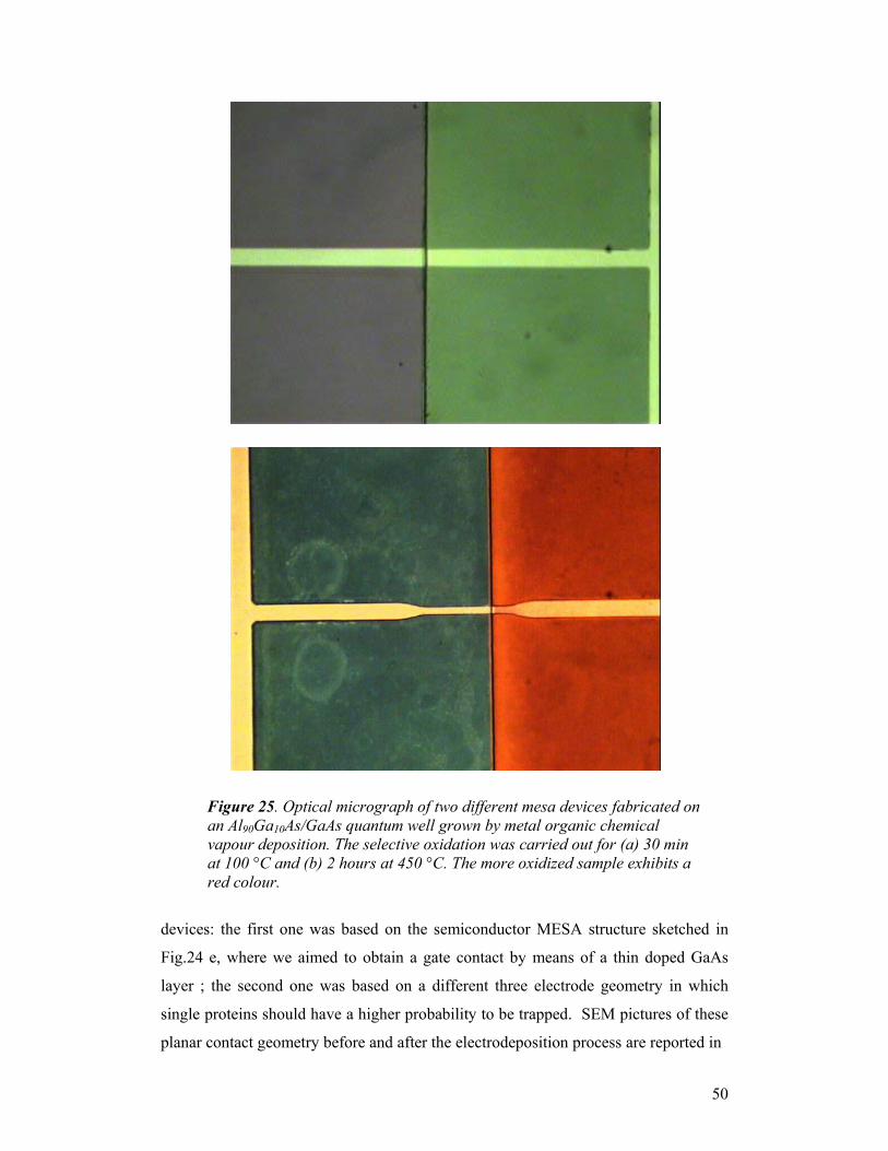
50
devices: the first one was based on the semiconductor MESA structure sketched in
Fig.24 e, where we aimed to obtain a gate contact by means of a thin doped GaAs
layer ; the second one was based on a different three electrode geometry in which
single proteins should have a higher probability to be trapped. SEM pictures of these
planar contact geometry before and after the electrodeposition process are reported in
Figure 25. Optical micrograph of two different mesa devices fabricated on an Al90Ga10As/GaAs quantum well grown by metal organic chemical vapour deposition. The selective oxidation was carried out for (a) 30 min at 100 °C and (b) 2 hours at 450 °C. The more oxidized sample exhibits a red colour.
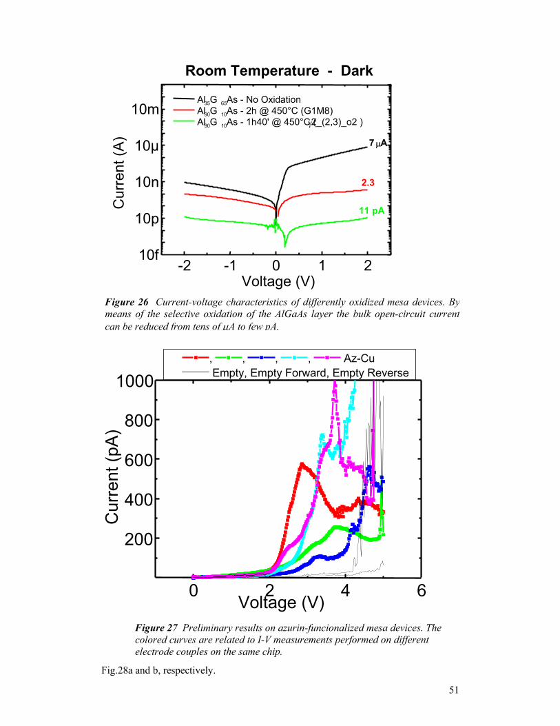
51
Fig.28a and b, respectively.
-2 -1 0 1 210f
10p
10n
10µ
10m
11 pA
2.3
7 µA
Room Temperature - Dark
Cur
rent
(A)
Voltage (V)
Al 35 G 65As - No Oxidation Al 90 G 10As - 2h @ 450°C (G1M8) Al 90 G 10As - 1h40' @ 450°C ( γ2_(2,3)_o2 )
Figure 26 Current-voltage characteristics of differently oxidized mesa devices. Bymeans of the selective oxidation of the AlGaAs layer the bulk open-circuit currentcan be reduced from tens of µA to few pA.
0 2 4 6
200
400
600
800
1000
Cur
rent
(pA
)
Voltage (V)
, , , , Az-Cu Empty, Empty Forward, Empty Reverse
Figure 27 Preliminary results on azurin-funcionalized mesa devices. The colored curves are related to I-V measurements performed on different electrode couples on the same chip.
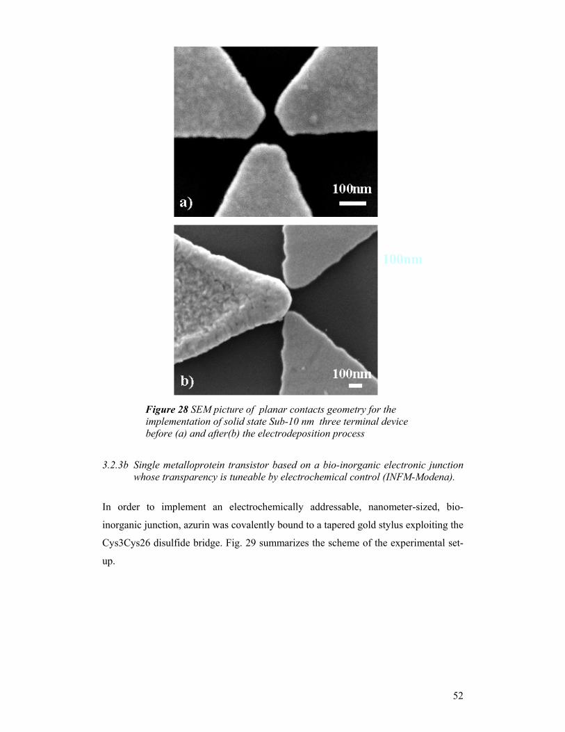
52
3.2.3b Single metalloprotein transistor based on a bio-inorganic electronic junction
whose transparency is tuneable by electrochemical control (INFM-Modena).
In order to implement an electrochemically addressable, nanometer-sized, bio-
inorganic junction, azurin was covalently bound to a tapered gold stylus exploiting the
Cys3Cys26 disulfide bridge. Fig. 29 summarizes the scheme of the experimental set-
up.
100nm
Figure 28 SEM picture of planar contacts geometry for the implementation of solid state Sub-10 nm three terminal device before (a) and after(b) the electrodeposition process
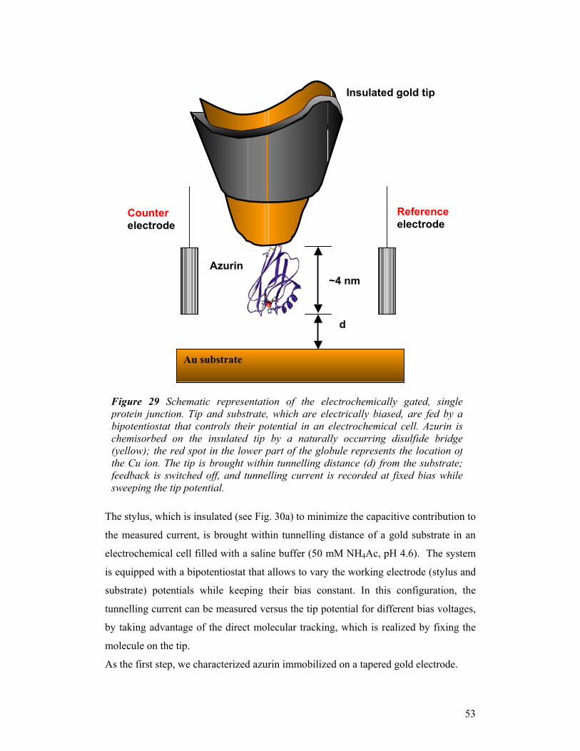
53
The stylus, which is insulated (see Fig. 30a) to minimize the capacitive contribution to
the measured current, is brought within tunnelling distance of a gold substrate in an
electrochemical cell filled with a saline buffer (50 mM NH4Ac, pH 4.6). The system
is equipped with a bipotentiostat that allows to vary the working electrode (stylus and
substrate) potentials while keeping their bias constant. In this configuration, the
tunnelling current can be measured versus the tip potential for different bias voltages,
by taking advantage of the direct molecular tracking, which is realized by fixing the
molecule on the tip.
As the first step, we characterized azurin immobilized on a tapered gold electrode.
Au substrate
~4 nm
d
Insulated gold tip
Reference electrode
Counter electrode
Azurin
Figure 29 Schematic representation of the electrochemically gated, singleprotein junction. Tip and substrate, which are electrically biased, are fed by abipotentiostat that controls their potential in an electrochemical cell. Azurin ischemisorbed on the insulated tip by a naturally occurring disulfide bridge(yellow); the red spot in the lower part of the globule represents the location ofthe Cu ion. The tip is brought within tunnelling distance (d) from the substrate;feedback is switched off, and tunnelling current is recorded at fixed bias whilesweeping the tip potential.
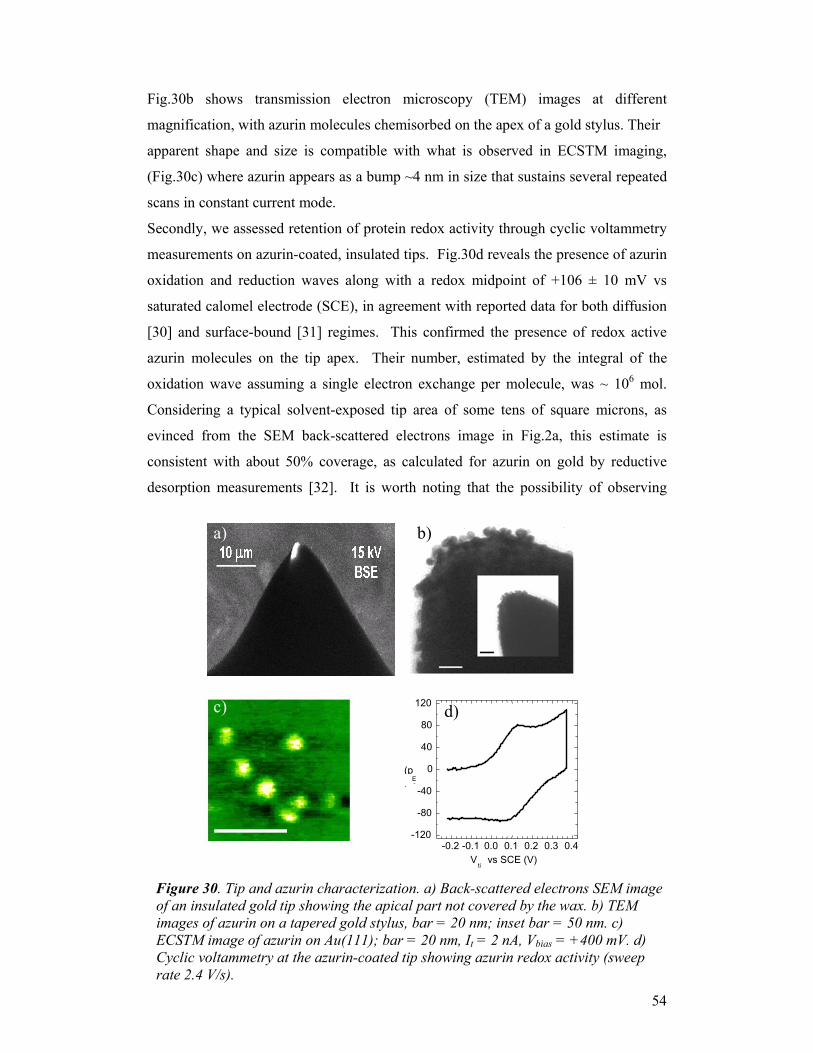
54
Fig.30b shows transmission electron microscopy (TEM) images at different
magnification, with azurin molecules chemisorbed on the apex of a gold stylus. Their
apparent shape and size is compatible with what is observed in ECSTM imaging,
(Fig.30c) where azurin appears as a bump ~4 nm in size that sustains several repeated
scans in constant current mode.
Secondly, we assessed retention of protein redox activity through cyclic voltammetry
measurements on azurin-coated, insulated tips. Fig.30d reveals the presence of azurin
oxidation and reduction waves along with a redox midpoint of +106 ± 10 mV vs
saturated calomel electrode (SCE), in agreement with reported data for both diffusion
[30] and surface-bound [31] regimes. This confirmed the presence of redox active
azurin molecules on the tip apex. Their number, estimated by the integral of the
oxidation wave assuming a single electron exchange per molecule, was ~ 106 mol.
Considering a typical solvent-exposed tip area of some tens of square microns, as
evinced from the SEM back-scattered electrons image in Fig.2a, this estimate is
consistent with about 50% coverage, as calculated for azurin on gold by reductive
desorption measurements [32]. It is worth noting that the possibility of observing
Figure 30. Tip and azurin characterization. a) Back-scattered electrons SEM image of an insulated gold tip showing the apical part not covered by the wax. b) TEM images of azurin on a tapered gold stylus, bar = 20 nm; inset bar = 50 nm. c) ECSTM image of azurin on Au(111); bar = 20 nm, It = 2 nA, Vbias = +400 mV. d) Cyclic voltammetry at the azurin-coated tip showing azurin redox activity (sweep rate 2.4 V/s).
-0.2 -0.1 0.0 0.1 0.2 0.3 0.4 -120
-80
-40
0
40
80
120
IEC
(p
Vti
vs SCE (V)
a) b)
c) d)
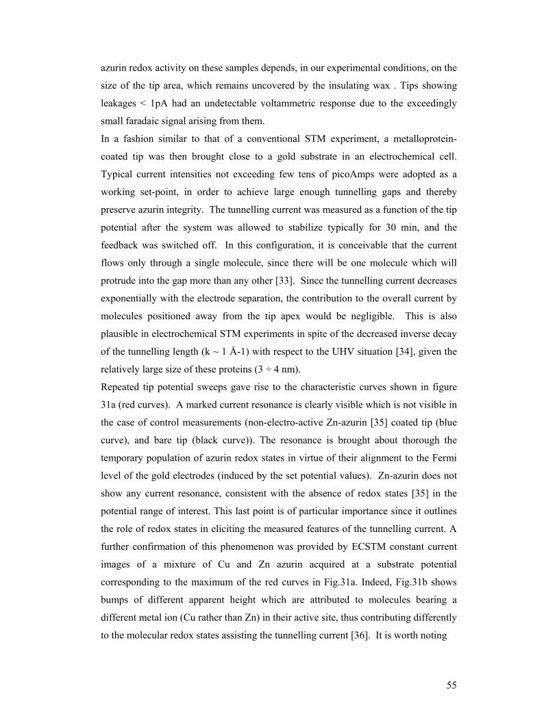
55
azurin redox activity on these samples depends, in our experimental conditions, on the
size of the tip area, which remains uncovered by the insulating wax . Tips showing
leakages < 1pA had an undetectable voltammetric response due to the exceedingly
small faradaic signal arising from them.
In a fashion similar to that of a conventional STM experiment, a metalloprotein-
coated tip was then brought close to a gold substrate in an electrochemical cell.
Typical current intensities not exceeding few tens of picoAmps were adopted as a
working set-point, in order to achieve large enough tunnelling gaps and thereby
preserve azurin integrity. The tunnelling current was measured as a function of the tip
potential after the system was allowed to stabilize typically for 30 min, and the
feedback was switched off. In this configuration, it is conceivable that the current
flows only through a single molecule, since there will be one molecule which will
protrude into the gap more than any other [33]. Since the tunnelling current decreases
exponentially with the electrode separation, the contribution to the overall current by
molecules positioned away from the tip apex would be negligible. This is also
plausible in electrochemical STM experiments in spite of the decreased inverse decay
of the tunnelling length (k ~ 1 Å-1) with respect to the UHV situation [34], given the
relatively large size of these proteins (3 ÷ 4 nm).
Repeated tip potential sweeps gave rise to the characteristic curves shown in figure
31a (red curves). A marked current resonance is clearly visible which is not visible in
the case of control measurements (non-electro-active Zn-azurin [35] coated tip (blue
curve), and bare tip (black curve)). The resonance is brought about thorough the
temporary population of azurin redox states in virtue of their alignment to the Fermi
level of the gold electrodes (induced by the set potential values). Zn-azurin does not
show any current resonance, consistent with the absence of redox states [35] in the
potential range of interest. This last point is of particular importance since it outlines
the role of redox states in eliciting the measured features of the tunnelling current. A
further confirmation of this phenomenon was provided by ECSTM constant current
images of a mixture of Cu and Zn azurin acquired at a substrate potential
corresponding to the maximum of the red curves in Fig.31a. Indeed, Fig.31b shows
bumps of different apparent height which are attributed to molecules bearing a
different metal ion (Cu rather than Zn) in their active site, thus contributing differently
to the molecular redox states assisting the tunnelling current [36]. It is worth noting
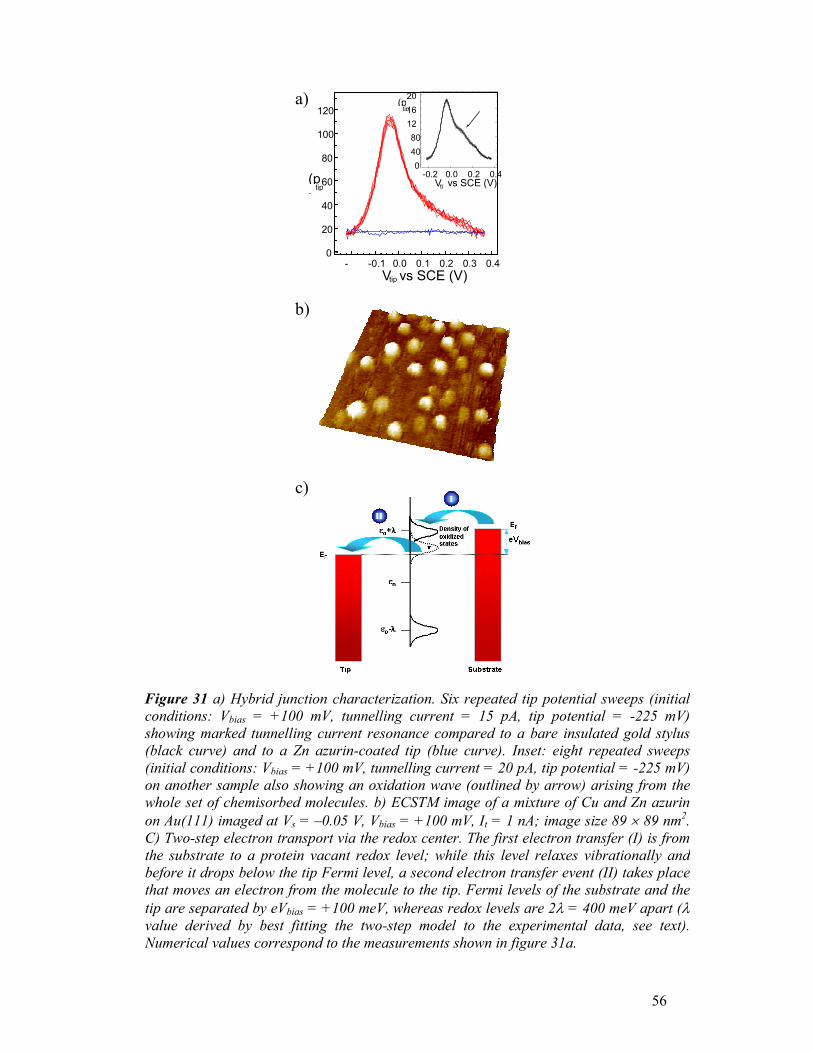
56
- -0.1 0.0 0.1 0.2 0.3 0.40
20
40
60
80
100
120
Itip
(p
Vtip vs SCE (V)
-0.2 0.0 0.2 0.40
4080
121620
Vti vs SCE (V)
Itip
(pa)
b)
c)
Figure 31 a) Hybrid junction characterization. Six repeated tip potential sweeps (initialconditions: Vbias = +100 mV, tunnelling current = 15 pA, tip potential = -225 mV)showing marked tunnelling current resonance compared to a bare insulated gold stylus(black curve) and to a Zn azurin-coated tip (blue curve). Inset: eight repeated sweeps(initial conditions: Vbias = +100 mV, tunnelling current = 20 pA, tip potential = -225 mV)on another sample also showing an oxidation wave (outlined by arrow) arising from thewhole set of chemisorbed molecules. b) ECSTM image of a mixture of Cu and Zn azurinon Au(111) imaged at Vs = –0.05 V, Vbias = +100 mV, It = 1 nA; image size 89 × 89 nm2.C) Two-step electron transport via the redox center. The first electron transfer (I) is from the substrate to a protein vacant redox level; while this level relaxes vibrationally andbefore it drops below the tip Fermi level, a second electron transfer event (II) takes placethat moves an electron from the molecule to the tip. Fermi levels of the substrate and thetip are separated by eVbias = +100 meV, whereas redox levels are 2λ = 400 meV apart (λvalue derived by best fitting the two-step model to the experimental data, see text).Numerical values correspond to the measurements shown in figure 31a.
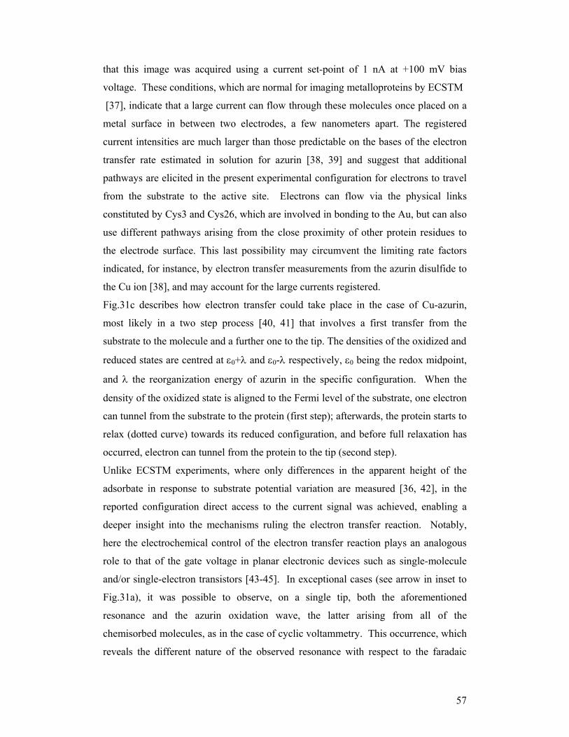
57
that this image was acquired using a current set-point of 1 nA at +100 mV bias
voltage. These conditions, which are normal for imaging metalloproteins by ECSTM
[37], indicate that a large current can flow through these molecules once placed on a
metal surface in between two electrodes, a few nanometers apart. The registered
current intensities are much larger than those predictable on the bases of the electron
transfer rate estimated in solution for azurin [38, 39] and suggest that additional
pathways are elicited in the present experimental configuration for electrons to travel
from the substrate to the active site. Electrons can flow via the physical links
constituted by Cys3 and Cys26, which are involved in bonding to the Au, but can also
use different pathways arising from the close proximity of other protein residues to
the electrode surface. This last possibility may circumvent the limiting rate factors
indicated, for instance, by electron transfer measurements from the azurin disulfide to
the Cu ion [38], and may account for the large currents registered.
Fig.31c describes how electron transfer could take place in the case of Cu-azurin,
most likely in a two step process [40, 41] that involves a first transfer from the
substrate to the molecule and a further one to the tip. The densities of the oxidized and
reduced states are centred at ε0+λ and ε0-λ respectively, ε0 being the redox midpoint,
and λ the reorganization energy of azurin in the specific configuration. When the
density of the oxidized state is aligned to the Fermi level of the substrate, one electron
can tunnel from the substrate to the protein (first step); afterwards, the protein starts to
relax (dotted curve) towards its reduced configuration, and before full relaxation has
occurred, electron can tunnel from the protein to the tip (second step).
Unlike ECSTM experiments, where only differences in the apparent height of the
adsorbate in response to substrate potential variation are measured [36, 42], in the
reported configuration direct access to the current signal was achieved, enabling a
deeper insight into the mechanisms ruling the electron transfer reaction. Notably,
here the electrochemical control of the electron transfer reaction plays an analogous
role to that of the gate voltage in planar electronic devices such as single-molecule
and/or single-electron transistors [43-45]. In exceptional cases (see arrow in inset to
Fig.31a), it was possible to observe, on a single tip, both the aforementioned
resonance and the azurin oxidation wave, the latter arising from all of the
chemisorbed molecules, as in the case of cyclic voltammetry. This occurrence, which
reveals the different nature of the observed resonance with respect to the faradaic
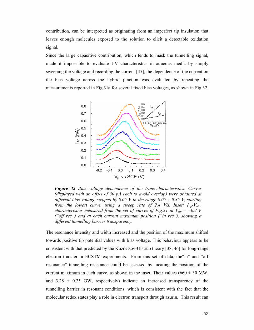
58
contribution, can be interpreted as originating from an imperfect tip insulation that
leaves enough molecules exposed to the solution to elicit a detectable oxidation
signal.
Since the large capacitive contribution, which tends to mask the tunnelling signal,
made it impossible to evaluate I-V characteristics in aqueous media by simply
sweeping the voltage and recording the current [45], the dependence of the current on
the bias voltage across the hybrid junction was evaluated by repeating the
measurements reported in Fig.31a for several fixed bias voltages, as shown in Fig.32.
The resonance intensity and width increased and the position of the maximum shifted
towards positive tip potential values with bias voltage. This behaviour appears to be
consistent with that predicted by the Kuznetsov-Ulstrup theory [38, 46] for long-range
electron transfer in ECSTM experiments. From this set of data, the“in” and “off
resonance” tunnelling resistance could be assessed by locating the position of the
current maximum in each curve, as shown in the inset. Their values (660 ± 30 MW,
and 3.28 ± 0.25 GW, respectively) indicate an increased transparency of the
tunnelling barrier in resonant conditions, which is consistent with the fact that the
molecular redox states play a role in electron transport through azurin. This result can
Figure 32 Bias voltage dependence of the trans-characteristics. Curves(displayed with an offset of 50 pA each to avoid overlap) were obtained atdifferent bias voltage stepped by 0.05 V in the range 0.05 ÷ 0.35 V, startingfrom the lowest curve, using a sweep rate of 2.4 V/s. Inset: Itip-Vbiascharacteristics measured from the set of curves of Fig.31 at Vtip = –0.2 V(“off res”) and at each current maximum position (“in res”), showing adifferent tunnelling barrier transparency.
-0.2 -0.1 0.0 0.1 0.2 0.3 0.40.0 0.1 0.2 0.3 0.4 0.5 0.6 0.7 0.8
I tip (n
A)
Vti vs SCE (V)
Vbias 0.0 0.1 0.2 0.3 0.4
0.00.10.20.30.40.5
Ioff
Iin
I tip (n
A)
(V)
59
be exploited to modulate the current flow through the protein-hosting junction in a
fashion pretty much similar to that of a single particle transistor.
Furthermore, it has been discovered that the tip potential value at which the current
maximum occurs depends linearly on the applied bias. A best fit of the
aforementioned theory for two-step vibrationally coherent electron transfer in
ECSTM of redox adsorbates [40] to the observed data provided an estimate for the
numerical coefficient that determines the potential value at the redox center within the
tunnelling gap [40]. A figure of 0.40 ± 0.03 was obtained, confirming experimentally
for the first time the assumption, usually made in ECSTM data analysis [41], that the
redox couple potential lies approximately halfway through the bias voltage drop. The
model also provides an estimate for the reorganization energy λ at about 200 meV.
This figure is substantially lower than that measured for azurin in solution [47],
consistent with other ECSTM observations [42] and theoretical estimates [40].
Besides, it is worth noting that it compares well with theoretical estimates for the
reorganization energy of azurin inner shell [48]. Indeed, a reduced λ value in our
experiments may be ascribed to the particular configuration whereby two closely
spaced electrodes, sandwiching azurin, prevent most water molecules from
surrounding the protein, cancelling, thus, the solvent contribution to λ.
It is worth noting that both the present resonant-like behaviour and that previously
observed, characterized by the occurrence of a current plateau upon variation of the
substrate potential, are interpretable within the two-step electron transfer theory.
Observing either of the two regimes depends just upon the relative value of eVbias and
2λ.
The reported results demonstrate the possibility of exploiting metalloprotein redox
properties to vary the electronic transparency of a wet bio-inorganic junction made
even with a single molecule hosted in a nanometer gap. The demonstration of a
protein-based tuneable electronic gate is a critical step in the implementation of single
particle transistors made with metalloproteins and could represent a paradigm for
devising future nanobioelectronic devices.
References:
[1] G. Maruccio et al., submitted to Adv. Mat.
60
[2] We call our protein device a field effect transistor since we exploit a field effect to modulate the resistance of the protein monolayer and change the I-V characteristics of the device.
[3] J. Lee et al., Nano Letters 2003, 3, 113; C. R. Kagan et al., Nano Letters 2003, 3, 119 [4] R.M.Metzger, B.Chen, U.Hopfner, M.V.Lakshmikantham, D.Vuillaume, T.Kawai,
X.Wu, H.Tachibana, T.V.Hughes, H.Sakurai, J.W.Baldwin, C.Hosch, M.P.Cava, L.Brehmer, G.J.Ashwell, J. Am. Chem. Soc. 1997, 119, 10455
[5] S. Heinze, J. Tersoff, R. Martel, V. Derycke, J. Appenzeller, and Ph. Avouris Phys. Rev. Lett. 2002, 89, 106801
[6] O. Kuhn, V. Rupasov and S. Mukamel, J. Chem. Phys. 1996, 104, 5821 [7] IUPAC Compendium of Chemical Terminology 2nd Edition (1997) [8] D.N. Blauch and J.M. Saveant, J.Am.Chem.Soc. 1992, 114, 3323 [9] J.Park, A.N.Pasupathy,J.I.Goldsmith, C.Chang, Y.Yaish, J.R. Petta, M.Rinkoski,
J.P.Sethna, H.D.Abruna, P.L.McEuen and C.Ralph, Nature 2002, 417, 722 [10] P.Facci, D.Alliata, S. Cannistraro, Ultramicroscopy 2001, 89, 291 [11] A.Alessandrini, M.Gerunda, G.W. Canters, M.P. Verbeet, P. Facci, Chem. Phys. Lett.
2003, 376, 625 [12] P.Visconti, G.Maruccio, E.D'Amone, A.Della Torre, A.Bramanti, R.Cingolani,
R.Rinaldi, Mat. Sci. Eng. C-Bio S 23, 889-892 (2003) [13] Kroes, S.J. et al., Biophys J. 1998, 75, 2441-50. [14] Nar, H. et al., J. Mol. Biol. 1991, 221, 765-72. [15] Baker, E.N., J. Mol. Biol. 1988, 203, 1071-95. [16] Nar, H. et al., FEBS Lett. 1992, 306, 119-24. [17] Nar, H. et al., Eur. J . Biochem. 1992, 205, 1123-9. [18] Hansen, J.E. et al., Biochemistry 1990, 29, 7329-38. [19] Sweeney, J.A. et al., J. Am. Chem. Soc. 1991, 113, 7531-7. [20] Leckner, J. et al., Biochim. Biophys. Acta 1997, 1342, 19-27. [21] Larsson, S. et al., J. Phys. Chem. 1995, 99, 4860-5. [22] Merzel, F. et al., Proc. Natl. Acad. Sci. USA 2002, 99, 5378-83. [23] Danielewicz-Ferchmin, I. et al., Biophys. Chem. 2003, 106, 147-153. [24] Svergun, D.I. et al., Proc. Natl. Acad. Sci. USA 1998, 95, 2267-72. [25] Xu, D. et al., J. Phys. Chem. 1996, 100, 12108-21. [26] Pompa P.P. et al., Phys. Rev. E 69, 032901 (2004). [27] P.Visconti, G.Maruccio, E.D'Amone, A.Della Torre, A.Bramanti, R.Cingolani,
R.Rinaldi, Mat. Sci. Eng. C-Bio S 23, 889-892 (2003) [28] P.Visconti, G.Maruccio, E.D'Amone, A.Della Torre, A.Bramanti, R.Cingolani,
R.Rinaldi, Mat. Sci. Eng. C-Bio S 23, 889-892 (2003) [29] Krahne R. et al., Appl. Phys. Lett. 81, 730-732, 2002), [30] Sykes, A. G. Active-site properties of the blue copper proteins. Adv. Inorg. Chem. 36,
377-408 (1991). [31] Facci, P. Alliata, D. & Cannistraro, S. Potential-induced resonant tunneling through a
redox metalloprotein investigated by electrochemical scanning probe microscopy. Ultramicroscopy 89, 291-298 (2001).
[32] Chi, Q. et al. Molecular monolayers and interfacial electron transfer of Pseudomonas aeruginosa azurin on Au(111). J. Am. Chem. Soc. 122, 4047-4055 (2000).
[33] Klein, D. L. Roth, R. Lim, A. K. L. Alivisatos, A. P. & McEuen, P. L. A single-electron transistor made from a cadmium selenide nanocrystal. Nature, 389, 699-701 (1997).
[34] Vaught, A. Jing, T. W. & Lindsay, S. M. Non-exponential tunnelling in water near an electrode. Chem. Phys. Lett. 236, 206-310 (1995).
[35] van Amsterdam, I.M.C. et al. Effects of Dimerization on Protein Electron Transfer. Chemistry 7, 2398-2406 (2001).
[36] Alessandrini, A. Gerunda, M. Canters, G. W. Verbeet, M. Ph. & Facci, P. Electron tunnelling through azurin is mediated by the active site Cu ion. Chem. Phys. Lett. 376, 625-630 (2003).
61
[37] Friis, E. P. et al. An approach to long-range electron transfer mechanisms in metalloproteins: In situ scanning tunneling microscopy with submolecular resolution. Proc. Natl. Acad. Sci. USA 96, 1379-1384 (1999).
[38] Farver, O. & Pecht, I. Long range intramolecular electron transfer in azurins. J. Am. Chem. Soc. 114, 5764-5767 (1992).
[39] Gray, H. B. & Winkler J. R. Electron tunnelling through proteins. Q. Rev. Biophys. 36, 341-372 (2003).
[40] Friis, E. P. Kharkats, Y. I. Kuznetsov, A. M. & Ulstrup, J. In situ scanning tunnelling microscopy of a redox molecule as a vibrationally coherent electronic three-level process. J. Phys. Chem. A 102, 7851-7859 (1998).
[41] Han, W. et al. STM contrast, electron transfer chemistry, and conduction in molecules. J. Phys. Chem. B 101, 10719-10725 (1997).
[42] Tao, N. J. Probing potential-tuned resonant tunnelling through redox molecules with scanning tunnelling microscopy. Phys. Rev. Lett. 76, 4066-4069 (1996).
[43] Tans, S. J. Verschueren, A. R. M. & Dekker, C. Room-temperature transistor based on a single carbon nanotube. Nature 393, 49-52 (1998).
[44] Park, J. et al. Coulomb blockade and the Kondo effect in single-atom transistor. Nature 417, 722-725 (2002).
[45] Kubatkin, S. et al. Single-electron transistor of a single organic molecule with access to several redox states. Nature 425, 698-701 (2003).
[46] Zhang, J. et al. Electron transfer behaviour of biological macromolecules towards the single-molecule level. J. Phys.: Condens. Matter 15, S1873-S1890 (2003)
[47] Di Bilio, A.J. et al. Reorganization Energy of Blue Copper: Effects of Temperature and Driving Force on the Rates of Electron Transfer in Ruthenium- and Osmium-Modified Azurins. J. Am. Chem. Soc.; 119, 9921-9922 (1997).
[48] Ryde, U. & Olsson, M.H.M. Structure, Strain, and reorganization energy of blue copper models in the protein. Int. J. Quantum Chem. 81, 335-347 (2001).
62
3.3 WP3
The final goal of this workpackage was the implementation of metalloprotein based
biosensors. To this aim, specific deliverables (D3.1 and D3.2) and milestones (M10
and M11) were accomplished, concerning the testing of conductivity of molecular
layers under different environments, the study of the relationship between electronic
conduction and metalloprotein hydration, and the realization and characterization of a
nitrite biosensor. Different experimental methods were exploited for these studies,
ranging from protein design and synthesis (with the Leiden Group), to single molecule
characterization by scanning probe techniques, and cyclic voltammetry measurements
on the different protein layers. Spectroscopic studies and Molecular Dynamics
simulation on the metalloproteins were performed within this workpackage. Finally,
several approaches to obtain quantifiable nitrite turnover from electroanalyses of the
enzyme nitrite reductase are reported.
The experiments were performed by the groups of Oxford and INFM Viterbo, in
strong collaboration through student exchanges. The proteins were delivered by
Leiden.
3.3.1 Deliverable D3.1 (Milestones M10-M11): characterization of conductivity in
metalloproteins monolayers
Self-assembling and conductivity of Plastocyanin mutants (INFM-Viterbo)
INFM-Viterbo focused its attention on the design, spectroscopic analysis and single
molecule characterisation of copper protein plastocyanin mutants. The aim was to get
some insight into the electron transport mechanism at molecular level, which is a
fundamental task in building hydrid nanodevices/nanobiosensors, and to implement
the use of different metalloproteins (Fig.1) for interconnecting nanostructures.
The Viterbo group has closely collaborated with the Leiden group in the design and
engineering of two plastocyanin mutants able to bind selectively to a gold surface, by
exploiting either SS or SH groups. In the first mutant (PCSS), a disulfide bridge was
inserted within the protein (Fig. 1a) by replacing residues Ile-21 and Glu-25 with Cys
using structurally conservative mutagenesis. X-ray crystallography and several
spectroscopies (Resonance Raman, Electron Paramagnetic Resonance, UV-VIS)
indicated that the overall three-dimensional structure of PCSS and the redox copper
site coordination has been essentially preserved together with its electron transfer
properties [1, 5].
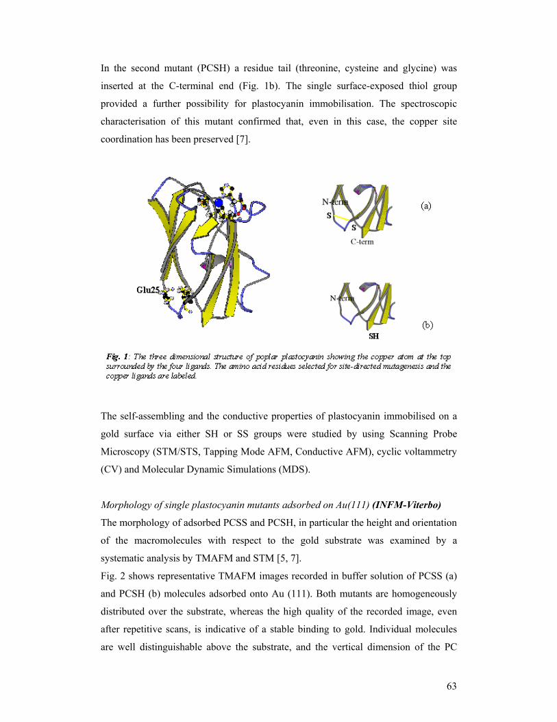
63
In the second mutant (PCSH) a residue tail (threonine, cysteine and glycine) was
inserted at the C-terminal end (Fig. 1b). The single surface-exposed thiol group
provided a further possibility for plastocyanin immobilisation. The spectroscopic
characterisation of this mutant confirmed that, even in this case, the copper site
coordination has been preserved [7].
The self-assembling and the conductive properties of plastocyanin immobilised on a
gold surface via either SH or SS groups were studied by using Scanning Probe
Microscopy (STM/STS, Tapping Mode AFM, Conductive AFM), cyclic voltammetry
(CV) and Molecular Dynamic Simulations (MDS).
Morphology of single plastocyanin mutants adsorbed on Au(111) (INFM-Viterbo)
The morphology of adsorbed PCSS and PCSH, in particular the height and orientation
of the macromolecules with respect to the gold substrate was examined by a
systematic analysis by TMAFM and STM [5, 7].
Fig. 2 shows representative TMAFM images recorded in buffer solution of PCSS (a)
and PCSH (b) molecules adsorbed onto Au (111). Both mutants are homogeneously
distributed over the substrate, whereas the high quality of the recorded image, even
after repetitive scans, is indicative of a stable binding to gold. Individual molecules
are well distinguishable above the substrate, and the vertical dimension of the PC
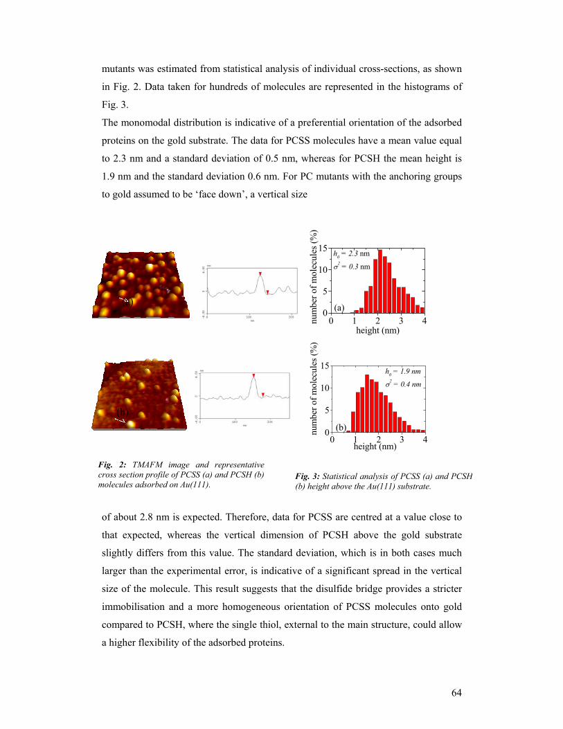
64
mutants was estimated from statistical analysis of individual cross-sections, as shown
in Fig. 2. Data taken for hundreds of molecules are represented in the histograms of
Fig. 3.
The monomodal distribution is indicative of a preferential orientation of the adsorbed
proteins on the gold substrate. The data for PCSS molecules have a mean value equal
to 2.3 nm and a standard deviation of 0.5 nm, whereas for PCSH the mean height is
1.9 nm and the standard deviation 0.6 nm. For PC mutants with the anchoring groups
to gold assumed to be ‘face down’, a vertical size
of about 2.8 nm is expected. Therefore, data for PCSS are centred at a value close to
that expected, whereas the vertical dimension of PCSH above the gold substrate
slightly differs from this value. The standard deviation, which is in both cases much
larger than the experimental error, is indicative of a significant spread in the vertical
size of the molecule. This result suggests that the disulfide bridge provides a stricter
immobilisation and a more homogeneous orientation of PCSS molecules onto gold
compared to PCSH, where the single thiol, external to the main structure, could allow
a higher flexibility of the adsorbed proteins.
0 1 2 3 40
5
10
15
(a)
h0 = 2.3 nm
σ2 = 0.3 nm
num
ber o
f mol
ecul
es (%
)
height (nm)
0 1 2 3 40
5
10
15
(b)
h0 = 1.9 nm
σ2 = 0.4 nm
height (nm)
num
ber o
f mol
ecul
es (%
)
Fig. 3: Statistical analysis of PCSS (a) and PCSH(b) height above the Au(111) substrate.
Fig. 2: TMAFM image and representativecross section profile of PCSS (a) and PCSH (b)molecules adsorbed on Au(111).
(b)
(a)
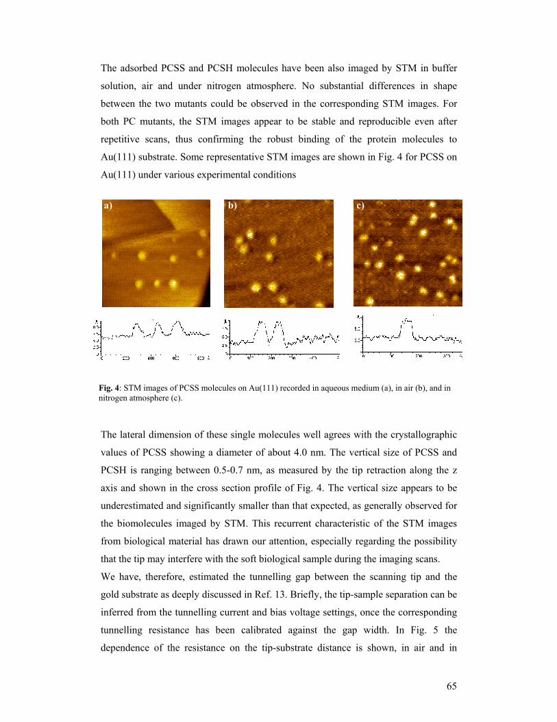
65
The adsorbed PCSS and PCSH molecules have been also imaged by STM in buffer
solution, air and under nitrogen atmosphere. No substantial differences in shape
between the two mutants could be observed in the corresponding STM images. For
both PC mutants, the STM images appear to be stable and reproducible even after
repetitive scans, thus confirming the robust binding of the protein molecules to
Au(111) substrate. Some representative STM images are shown in Fig. 4 for PCSS on
Au(111) under various experimental conditions
The lateral dimension of these single molecules well agrees with the crystallographic
values of PCSS showing a diameter of about 4.0 nm. The vertical size of PCSS and
PCSH is ranging between 0.5-0.7 nm, as measured by the tip retraction along the z
axis and shown in the cross section profile of Fig. 4. The vertical size appears to be
underestimated and significantly smaller than that expected, as generally observed for
the biomolecules imaged by STM. This recurrent characteristic of the STM images
from biological material has drawn our attention, especially regarding the possibility
that the tip may interfere with the soft biological sample during the imaging scans.
We have, therefore, estimated the tunnelling gap between the scanning tip and the
gold substrate as deeply discussed in Ref. 13. Briefly, the tip-sample separation can be
inferred from the tunnelling current and bias voltage settings, once the corresponding
tunnelling resistance has been calibrated against the gap width. In Fig. 5 the
dependence of the resistance on the tip-substrate distance is shown, in air and in
Fig. 4: STM images of PCSS molecules on Au(111) recorded in aqueous medium (a), in air (b), and in nitrogen atmosphere (c).
a) b) c)
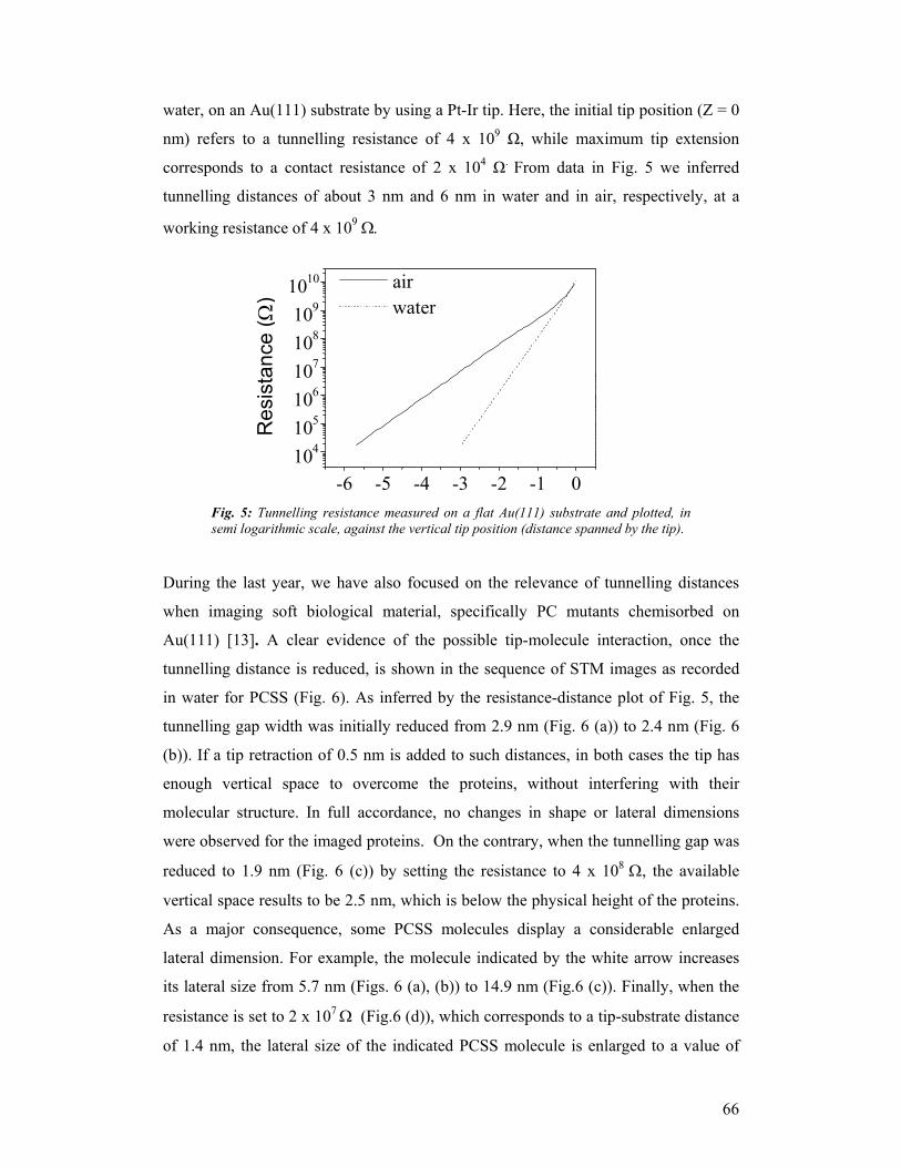
66
water, on an Au(111) substrate by using a Pt-Ir tip. Here, the initial tip position (Z = 0
nm) refers to a tunnelling resistance of 4 x 10⁹ Ω, while maximum tip extension
corresponds to a contact resistance of 2 x 10⁴ Ω. From data in Fig. 5 we inferred
tunnelling distances of about 3 nm and 6 nm in water and in air, respectively, at a
working resistance of 4 x 10⁹ Ω.
During the last year, we have also focused on the relevance of tunnelling distances
when imaging soft biological material, specifically PC mutants chemisorbed on
Au(111) [13]. A clear evidence of the possible tip-molecule interaction, once the
tunnelling distance is reduced, is shown in the sequence of STM images as recorded
in water for PCSS (Fig. 6). As inferred by the resistance-distance plot of Fig. 5, the
tunnelling gap width was initially reduced from 2.9 nm (Fig. 6 (a)) to 2.4 nm (Fig. 6
(b)). If a tip retraction of 0.5 nm is added to such distances, in both cases the tip has
enough vertical space to overcome the proteins, without interfering with their
molecular structure. In full accordance, no changes in shape or lateral dimensions
were observed for the imaged proteins. On the contrary, when the tunnelling gap was
reduced to 1.9 nm (Fig. 6 (c)) by setting the resistance to 4 x 10⁸ Ω, the available
vertical space results to be 2.5 nm, which is below the physical height of the proteins.
As a major consequence, some PCSS molecules display a considerable enlarged
lateral dimension. For example, the molecule indicated by the white arrow increases
its lateral size from 5.7 nm (Figs. 6 (a), (b)) to 14.9 nm (Fig.6 (c)). Finally, when the
resistance is set to 2 x 10⁷ Ω (Fig.6 (d)), which corresponds to a tip-substrate distance
of 1.4 nm, the lateral size of the indicated PCSS molecule is enlarged to a value of
-6 -5 -4 -3 -2 -1 0 10 4 10 5 10 6 10 7 10 8 10 9
10 10 R
esis
tanc
e ( Ω
) air water
Fig. 5: Tunnelling resistance measured on a flat Au(111) substrate and plotted, insemi logarithmic scale, against the vertical tip position (distance spanned by the tip).
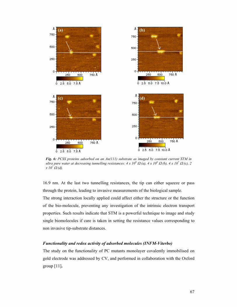
67
16.9 nm. At the last two tunnelling resistances, the tip can either squeeze or pass
through the protein, leading to invasive measurements of the biological sample.
The strong interaction locally applied could affect either the structure or the function
of the bio-molecule, preventing any investigation of the intrinsic electron transport
properties. Such results indicate that STM is a powerful technique to image and study
single biomolecules if care is taken in setting the resistance values corresponding to
non invasive tip-substrate distances.
Functionality and redox activity of adsorbed molecules (INFM-Viterbo)
The study on the functionality of PC mutants monolayer covalently immobilised on
gold electrode was addressed by CV, and performed in collaboration with the Oxford
group [11].
(a) (b)
(c) (d)
Fig. 6: PCSS proteins adsorbed on an Au(111) substrate as imaged by constant current STM inultra pure water at decreasing tunnelling resistances: 4 x 10⁹ Ω (a), 4 x 10⁸ Ω (b), 4 x 10⁷ Ω (c), 2 x 10⁷ Ω (d).
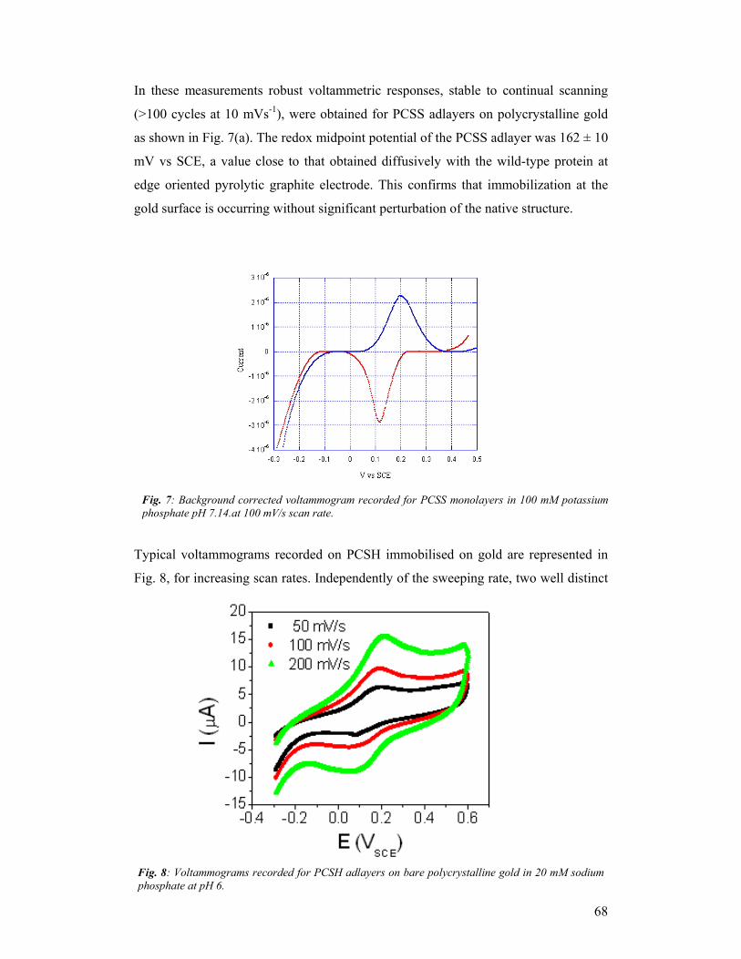
68
In these measurements robust voltammetric responses, stable to continual scanning
(>100 cycles at 10 mVs-1), were obtained for PCSS adlayers on polycrystalline gold
as shown in Fig. 7(a). The redox midpoint potential of the PCSS adlayer was 162 ± 10
mV vs SCE, a value close to that obtained diffusively with the wild-type protein at
edge oriented pyrolytic graphite electrode. This confirms that immobilization at the
gold surface is occurring without significant perturbation of the native structure.
Typical voltammograms recorded on PCSH immobilised on gold are represented in
Fig. 8, for increasing scan rates. Independently of the sweeping rate, two well distinct
Fig. 7: Background corrected voltammogram recorded for PCSS monolayers in 100 mM potassiumphosphate pH 7.14.at 100 mV/s scan rate.
Fig. 8: Voltammograms recorded for PCSH adlayers on bare polycrystalline gold in 20 mM sodiumphosphate at pH 6.
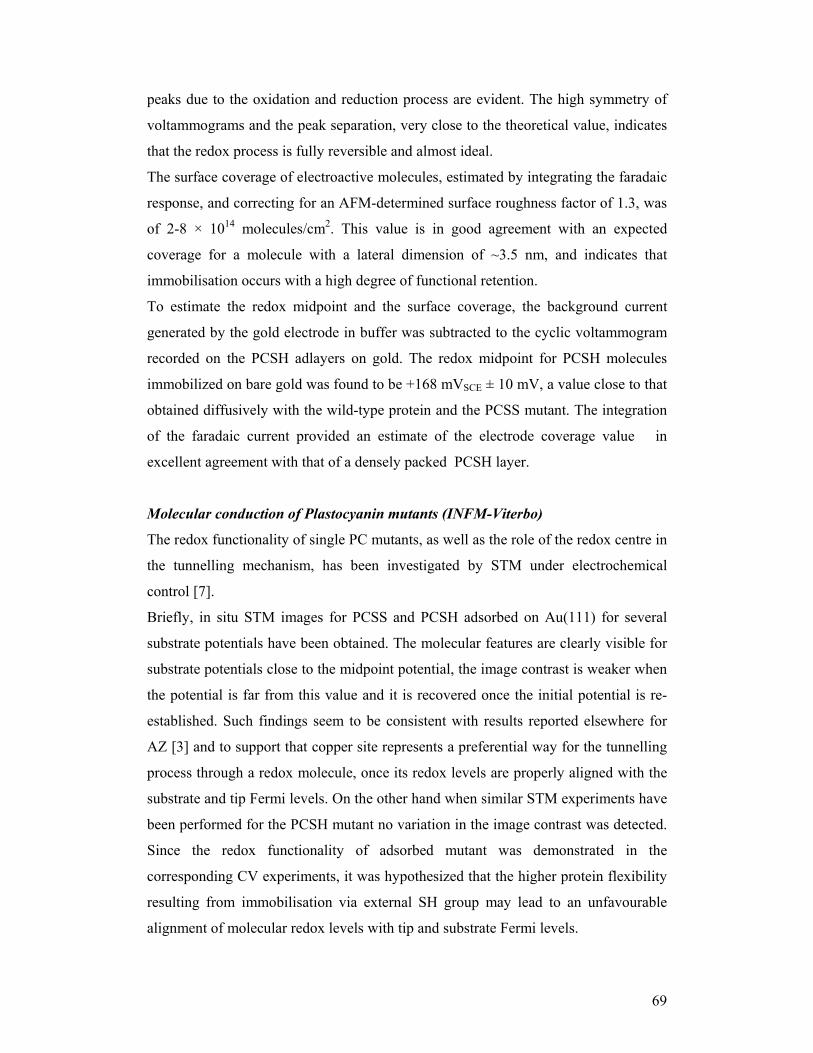
69
peaks due to the oxidation and reduction process are evident. The high symmetry of
voltammograms and the peak separation, very close to the theoretical value, indicates
that the redox process is fully reversible and almost ideal.
The surface coverage of electroactive molecules, estimated by integrating the faradaic
response, and correcting for an AFM-determined surface roughness factor of 1.3, was
of 2-8 × 10¹⁴ molecules/cm2. This value is in good agreement with an expected
coverage for a molecule with a lateral dimension of ~3.5 nm, and indicates that
immobilisation occurs with a high degree of functional retention.
To estimate the redox midpoint and the surface coverage, the background current
generated by the gold electrode in buffer was subtracted to the cyclic voltammogram
recorded on the PCSH adlayers on gold. The redox midpoint for PCSH molecules
immobilized on bare gold was found to be +168 mVSCE ± 10 mV, a value close to that
obtained diffusively with the wild-type protein and the PCSS mutant. The integration
of the faradaic current provided an estimate of the electrode coverage value in
excellent agreement with that of a densely packed PCSH layer.
Molecular conduction of Plastocyanin mutants (INFM-Viterbo)
The redox functionality of single PC mutants, as well as the role of the redox centre in
the tunnelling mechanism, has been investigated by STM under electrochemical
control [7].
Briefly, in situ STM images for PCSS and PCSH adsorbed on Au(111) for several
substrate potentials have been obtained. The molecular features are clearly visible for
substrate potentials close to the midpoint potential, the image contrast is weaker when
the potential is far from this value and it is recovered once the initial potential is re-
established. Such findings seem to be consistent with results reported elsewhere for
AZ [3] and to support that copper site represents a preferential way for the tunnelling
process through a redox molecule, once its redox levels are properly aligned with the
substrate and tip Fermi levels. On the other hand when similar STM experiments have
been performed for the PCSH mutant no variation in the image contrast was detected.
Since the redox functionality of adsorbed mutant was demonstrated in the
corresponding CV experiments, it was hypothesized that the higher protein flexibility
resulting from immobilisation via external SH group may lead to an unfavourable
alignment of molecular redox levels with tip and substrate Fermi levels.
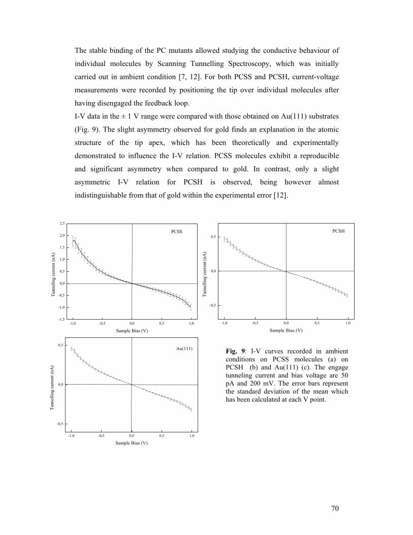
70
The stable binding of the PC mutants allowed studying the conductive behaviour of
individual molecules by Scanning Tunnelling Spectroscopy, which was initially
carried out in ambient condition [7, 12]. For both PCSS and PCSH, current-voltage
measurements were recorded by positioning the tip over individual molecules after
having disengaged the feedback loop.
I-V data in the ± 1 V range were compared with those obtained on Au(111) substrates
(Fig. 9). The slight asymmetry observed for gold finds an explanation in the atomic
structure of the tip apex, which has been theoretically and experimentally
demonstrated to influence the I-V relation. PCSS molecules exhibit a reproducible
and significant asymmetry when compared to gold. In contrast, only a slight
asymmetric I-V relation for PCSH is observed, being however almost
indistinguishable from that of gold within the experimental error [12].
-1,0 -0,5 0,0 0,5 1,0-1,5
-1,0
-0,5
0,0
0,5
1,0
1,5
2,0
2,5
PCSS
Tunn
elin
g cu
rrent
(nA
)
Sample Bias (V)
-1,0 -0,5 0,0 0,5 1,0
-0,5
0,0
0,5
PCSH
Tunn
ellin
g cu
rren
t (nA
)
Sample Bias (V)
Fig. 9: I-V curves recorded in ambientconditions on PCSS molecules (a) onPCSH (b) and Au(111) (c). The engagetunneling current and bias voltage are 50pA and 200 mV. The error bars representthe standard deviation of the mean whichhas been calculated at each V point.
-1,0 -0,5 0,0 0,5 1,0
-0,5
0,0
0,5
Au(111)
Tunn
ellin
g cu
rren
t (nA
)
Sample Bias (V)
71
Although both mutants seem to be electronically coupled to the electrode, the origin
of the observed differences is presently not clear.
In this connection, more recently, we have revisited the conduction properties of
PCSS and PCSH by STS and Conductive AFM (CAFM) in controlled environment
[12, 14].
STS analysis was performed under nitrogen atmosphere, to reduce the water layer at
the sample interface which may play a relevant role in tunnelling mechanism [12].
Fig. 10 shows that for both pure gold substrate and PCSH on gold, I-V curves closely
resemble those obtained under ambient conditions, whereas the asymmetry observed
for PCSS molecules has almost disappeared, with a concomitant decrease of the
recorded current.
-1,0 -0,5 0,0 0,5 1,0
-0,5
0,0
0,5PCSS
Tunn
ellin
g cu
rrent
(nA
)
Sample Bias (V)
-1,0 -0,5 0,0 0,5 1,0
-0,5
0,0
0,5
PCSHTu
nnel
ling
curre
nt (n
A)
Sample Bias (V)
Fig. 10: I-V curves recorded taken undernitrogen atmosphere on PCSS molecules(a) on PCSH (b) and Au(111) (c). Theengage tunneling current and bias voltageare 50 pA and 200 mV. The error barsrepresent the standard deviation of themean which has been calculated at each Vpoint.
-1,0 -0,5 0,0 0,5 1,0
-0,5
0,0
0,5Au(111)
Tunn
ellin
g cu
rrent
(nA
)
Sample Bias(V)
72
It can be reasonably assumed, therefore, that water molecules adsorbed at the sample-
tip interface are involved in generating the observed PCSS asymmetry. Nevertheless,
it appears intriguing that PCSH presents a symmetric I-V relation under both
experimental conditions. Indeed, it is hard to conceive that PCSH would retain a
different level of humidity with respect to the PCSS mutant.
We might perhaps invoke some differences between the orientation and interfacing of
the two mutant proteins with the electrode surface. In the case of PCSH, binding to
gold through the thiol group at the carboxy-terminal free end might lead to a less
hindered protein surface-electrode coupling than that obtained via the S-S bridge.
In order to investigate the influence of the tip-molecule gap on STS spectra, I-V
characteristics of tunnelling junctions, for different values of initial tunnelling current
were further measured [15].
I-V plots recorded at fixed location on PCSS molecules by varying the initial
tunnelling current are shown in Fig. 11. I-V response is asymmetric at all the engaging
tunnelling current values examined, even though the amount of rectification decreases
as the tunnelling current is raised. These data support a notable dependence of
conductive properties on tunnelling gap width.
We also expanded the voltage range to study the effect of the applied bias on the
electrical response. A sequence of I-V curves was recorded at the same location by
extending the bias range to ± 3 V (Fig. 12). An abrupt change was observed when
applying ± 3 V with a corresponding unusual increase in current flowing.
Nevertheless, the initial conductivity was recovered as soon as the bias range was
reduced below ± 2 V. This last finding indicates that at high voltages the bio-molecule
Fig. 11. I-V characteristicsrecorded by STS on a monolayer ofPCSS on Au(111) in ambientconditions. Each curve wasrecorded at a different initialtunnelling current.
73
was not damaged, but only subjected to transient phenomena induced by the strong
local electric field applied by the STM tip.
I-V characteristics recorded at 5 and 50 pA on PCSH molecules are shown in Fig. 13.
A highly asymmetric I-V response at low starting tunnelling current is observed, as
for the PCSS mutant. However, in contrast with what observed with PCSS, the
asymmetry completely disappears as the tunnelling gap is lowered.
In summary, the STS analysis performed on single molecule pointed out that the
protein molecule conduction properties are subtly affected by the water content and
are strongly dependent on the tunnelling gap width; with some role played by the
particular way in which the proteins assemble on the substrate.
Fig. 13: I-V characteristics as recorded by STS in ambient conditions on PCSH molecules chemisorbed on Au, starting bias 0.2V.
Fig. 12: I-V characteristics recordedby STM on PCSS molecules onAu(111) in ambient conditions, atincreasing bias voltage ranges ±1 V(green curve), ±1.5 V (purple curve), ±2 V (blue curve), ±2.5 V (red curve)and ±3 V (grey curve).
74
As concerns the tunnelling gap, the conductive properties of plastocyanin mutants
have been more controllably investigated by CAFM [14, 15]. In this case the AFM tip
is positioned in close contact with the protein molecules allowing also to probe
electronic properties of the plastocyanin mutants as a function of the applied forces.
The PCSS molecules were either immobilised on gold substrates and contacted with a
gold coated tip (Fig.14a) or alternatively adsorbed on gold coated AFM tip which was
brought in contact with a flat gold surface (Fig.14b).
I-V characteristics of the PCSS immobilised on gold substrates have been recorded in
air at room temperature. For a restricted bias region (± 0.05 V), a pure ohmic I-V
relation was found for different applied forces (Fig. 15). At similar forces, as the bias
(a) (b)
Fig. 14: Schematic representation of tip-PCSS-gold substrate junctions obtained by immobilizing PCSSwith the engineered SS group either on gold substrate (a) or on gold coated tip (b). In the first case thejunction is formed by bringing the tip into contact with the protein molecules, whereas in the second casethe PCSS modified tip is approached to a flat gold surface until a physical contact is established.
-0.04 -0.02 0.00 0.02 0.04-0.010
-0.005
0.000
0.005
0.010
Cur
rent
/nA
Bias/V
-0.3 -0.2 -0.1 0.0 0.1 0.2 0.3-0.15
-0.10
-0.05
0.00
0.05
0.10
0.15
Fig. 15: I-V characteristics over ±0.05V, measured in ambient condition, for a gold coated AFM tip in contact with PCSS molecules immobilized on Au(111) substrate at applied loads of 2nN (open circle), 4nN (dashed line), 8nN (solid line). Inset shows the sigmoidal I-V relation over ± 0.3V for 2nN(open circle), 4nN (dashed line), 8nN (solid line) .
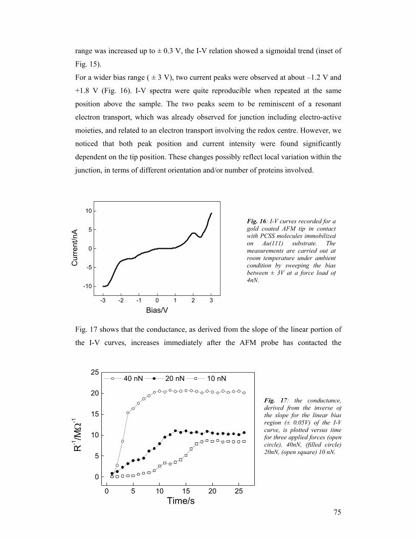
75
range was increased up to ± 0.3 V, the I-V relation showed a sigmoidal trend (inset of
Fig. 15).
For a wider bias range ( ± 3 V), two current peaks were observed at about –1.2 V and
+1.8 V (Fig. 16). I-V spectra were quite reproducible when repeated at the same
position above the sample. The two peaks seem to be reminiscent of a resonant
electron transport, which was already observed for junction including electro-active
moieties, and related to an electron transport involving the redox centre. However, we
noticed that both peak position and current intensity were found significantly
dependent on the tip position. These changes possibly reflect local variation within the
junction, in terms of different orientation and/or number of proteins involved.
Fig. 17 shows that the conductance, as derived from the slope of the linear portion of
the I-V curves, increases immediately after the AFM probe has contacted the
-3 -2 -1 0 1 2 3
-10
-5
0
5
10
Cur
rent
/nA
Bias/V
Fig. 16: I-V curves recorded for agold coated AFM tip in contactwith PCSS molecules immobilizedon Au(111) substrate. Themeasurements are carried out atroom temperature under ambientcondition by sweeping the biasbetween ± 3V at a force load of4nN.
Fig. 17: the conductance,derived from the inverse ofthe slope for the linear biasregion (± 0.05V) of the I-Vcurve, is plotted versus timefor three applied forces (opencircle), 40nN, (filled circle)20nN, (open square) 10 nN.
0 5 10 15 20 25
0
5
10
15
20
25
R-1/M
Ω-1
Time/s
40 nN 20 nN 10 nN
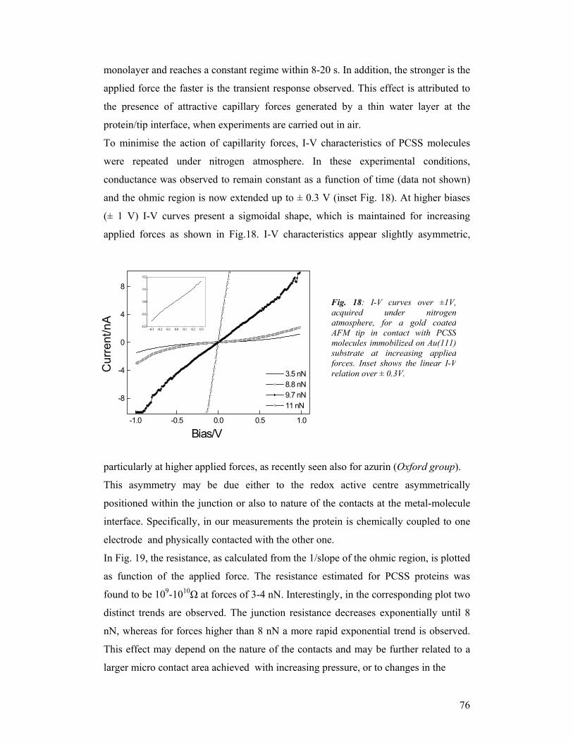
76
monolayer and reaches a constant regime within 8-20 s. In addition, the stronger is the
applied force the faster is the transient response observed. This effect is attributed to
the presence of attractive capillary forces generated by a thin water layer at the
protein/tip interface, when experiments are carried out in air.
To minimise the action of capillarity forces, I-V characteristics of PCSS molecules
were repeated under nitrogen atmosphere. In these experimental conditions,
conductance was observed to remain constant as a function of time (data not shown)
and the ohmic region is now extended up to ± 0.3 V (inset Fig. 18). At higher biases
(± 1 V) I-V curves present a sigmoidal shape, which is maintained for increasing
applied forces as shown in Fig.18. I-V characteristics appear slightly asymmetric,
particularly at higher applied forces, as recently seen also for azurin (Oxford group).
This asymmetry may be due either to the redox active centre asymmetrically
positioned within the junction or also to nature of the contacts at the metal-molecule
interface. Specifically, in our measurements the protein is chemically coupled to one
electrode and physically contacted with the other one.
In Fig. 19, the resistance, as calculated from the 1/slope of the ohmic region, is plotted
as function of the applied force. The resistance estimated for PCSS proteins was
found to be 109-1010Ω at forces of 3-4 nN. Interestingly, in the corresponding plot two
distinct trends are observed. The junction resistance decreases exponentially until 8
nN, whereas for forces higher than 8 nN a more rapid exponential trend is observed.
This effect may depend on the nature of the contacts and may be further related to a
larger micro contact area achieved with increasing pressure, or to changes in the
-1.0 -0.5 0.0 0.5 1.0
-8
-4
0
4
8
3.5 nN 8.8 nN 9.7 nN 11 nN
Cur
rent
/nA
Bias/V
-0.3 -0.2 -0.1 0.0 0.1 0.2 0.3-0.2
-0.1
0.0
0.1
0.2
Fig. 18: I-V curves over ±1V, acquired under nitrogen atmosphere, for a gold coated AFM tip in contact with PCSS molecules immobilized on Au(111) substrate at increasing applied forces. Inset shows the linear I-V relation over ± 0.3V.
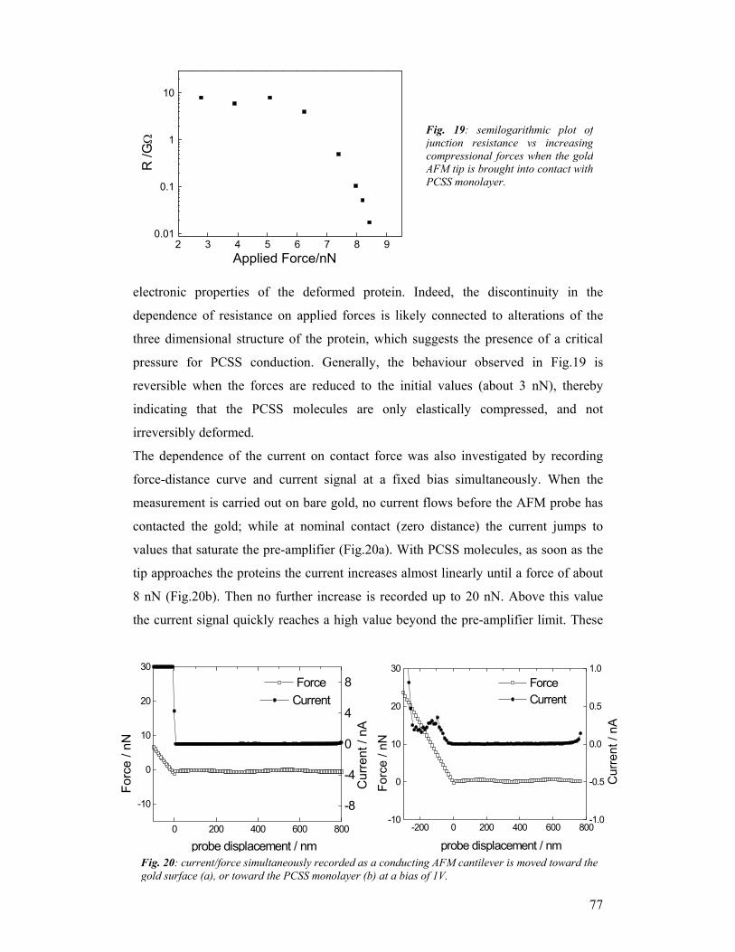
77
electronic properties of the deformed protein. Indeed, the discontinuity in the
dependence of resistance on applied forces is likely connected to alterations of the
three dimensional structure of the protein, which suggests the presence of a critical
pressure for PCSS conduction. Generally, the behaviour observed in Fig.19 is
reversible when the forces are reduced to the initial values (about 3 nN), thereby
indicating that the PCSS molecules are only elastically compressed, and not
irreversibly deformed.
The dependence of the current on contact force was also investigated by recording
force-distance curve and current signal at a fixed bias simultaneously. When the
measurement is carried out on bare gold, no current flows before the AFM probe has
contacted the gold; while at nominal contact (zero distance) the current jumps to
values that saturate the pre-amplifier (Fig.20a). With PCSS molecules, as soon as the
tip approaches the proteins the current increases almost linearly until a force of about
8 nN (Fig.20b). Then no further increase is recorded up to 20 nN. Above this value
the current signal quickly reaches a high value beyond the pre-amplifier limit. These
2 3 4 5 6 7 8 90.01
0.1
1
10
R /G
Ω
Applied Force/nN
Fig. 19: semilogarithmic plot ofjunction resistance vs increasingcompressional forces when the goldAFM tip is brought into contact withPCSS monolayer.
0 200 400 600 800
-10
0
10
20
30
Force
probe displacement / nm
Forc
e / n
N
-8
-4
0
4
8
Current
Cur
rent
/ nA
-200 0 200 400 600 800-10
0
10
20
30
Force Current
probe displacement / nm
Forc
e / n
N
-1.0
-0.5
0.0
0.5
1.0
Cur
rent
/ nA
Fig. 20: current/force simultaneously recorded as a conducting AFM cantilever is moved toward the gold surface (a), or toward the PCSS monolayer (b) at a bias of 1V.
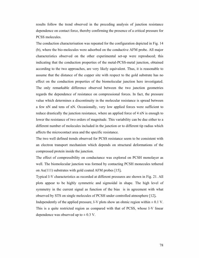
78
results follow the trend observed in the preceding analysis of junction resistance
dependence on contact force, thereby confirming the presence of a critical pressure for
PCSS molecules.
The conduction characterisation was repeated for the configuration depicted in Fig. 14
(b), where the bio-molecules were adsorbed on the conductive AFM probe. All major
characteristics observed on the other experimental set-up were reproduced; this
indicating that the conduction properties of the metal-PCSS-metal junction, obtained
according to the two approaches, are very likely equivalent. Thus, it is reasonable to
assume that the distance of the copper site with respect to the gold substrate has no
effect on the conduction properties of the biomolecular junction here investigated.
The only remarkable difference observed between the two junction geometries
regards the dependence of resistance on compressional forces. In fact, the pressure
value which determines a discontinuity in the molecular resistance is spread between
a few nN and tens of nN. Occasionally, very low applied forces were sufficient to
reduce drastically the junction resistance, where an applied force of 4 nN is enough to
lower the resistance of two orders of magnitude. This variability can be due either to a
different number of molecules included in the junction or to different tip radius which
affects the microcontact area and the specific resistance.
The two well defined trends observed for PCSS resistance seem to be consistent with
an electron transport mechanism which depends on structural deformations of the
compressed protein inside the junction.
The effect of compressibility on conductance was explored on PCSH monolayer as
well. The biomolecular junction was formed by contacting PCSH monecules tethered
on Au(111) substrates with gold coated AFM probes [15].
Typical I-V characteristics as recorded at different pressures are shown in Fig. 21. All
plots appear to be highly symmetric and sigmoidal in shape. The high level of
symmetry in the current signal as function of the bias is in agreement with what
observed by STS on single molecules of PCSH under controlled atmosphere [12].
Independently of the applied pressure, I-V plots show an ohmic region within ± 0.1 V.
This is a quite restricted region as compared with that of PCSS, whose I-V linear
dependence was observed up to ± 0.3 V.
79
The resistance of the protein has been studied also as a function of the force exercised
by the conducting AFM probe. Fig. 22 shows that over a range of 15 nN, resistance of
the bio-molecular junction decreases upon increasing the force. Even for this PC
mutant, the resistance is scaling with two distinct exponential laws. As seen for PCSS,
the presence of such discontinuity in the resistance–force dependence confirms the
occurrence of an electron transport mechanism dependent on structural deformations
of the compressed proteins inside the junction [14, 15].
Optical Spectroscopy (INFM-Viterbo)
The electron transfer process depends on several parameters which sometimes are
difficult to estimate; one of which being the reorganisation energy λ of the nuclear
degree of freedom. Calculation of this energy requires a knowledge of the coupling
strength of the protein vibrations to the electron transfer event. To get some insight on
such a parameter we have previously performed femtosecond laser pump-probe
experiments on azurin [4]. More recently, we have extended such a study to copper
protein plastocyanin [10].
Due to its wide spectral content, a femtosecond pump pulse creates a population in the
excited electronic state and vibrational coherence in both the ground and excited
states. A delayed probe pulse interrogates the sample and additional information (with
respect to traditional Raman) can be obtained. The evolution of the signal is therefore
modulated by the dynamics of the vibrational states. Suitable processing of this signal
-1.0 -0.5 0.0 0.5 1.0
-2
-1
0
1
2
Cur
rent
(nA
)
Bias (V)
4 nN 6 nN 8 nN 10 nN
Fig. 21: I-V characteristics as recorded by CAFMon PCSH molecules chemisorbed on Au(111) undernitrogen atmosphere.
Fig. 22: Semi logarithmic plot of resistance vs applied forces obtained by CAFM on a PCSH monolayer under nitrogen atmosphere.
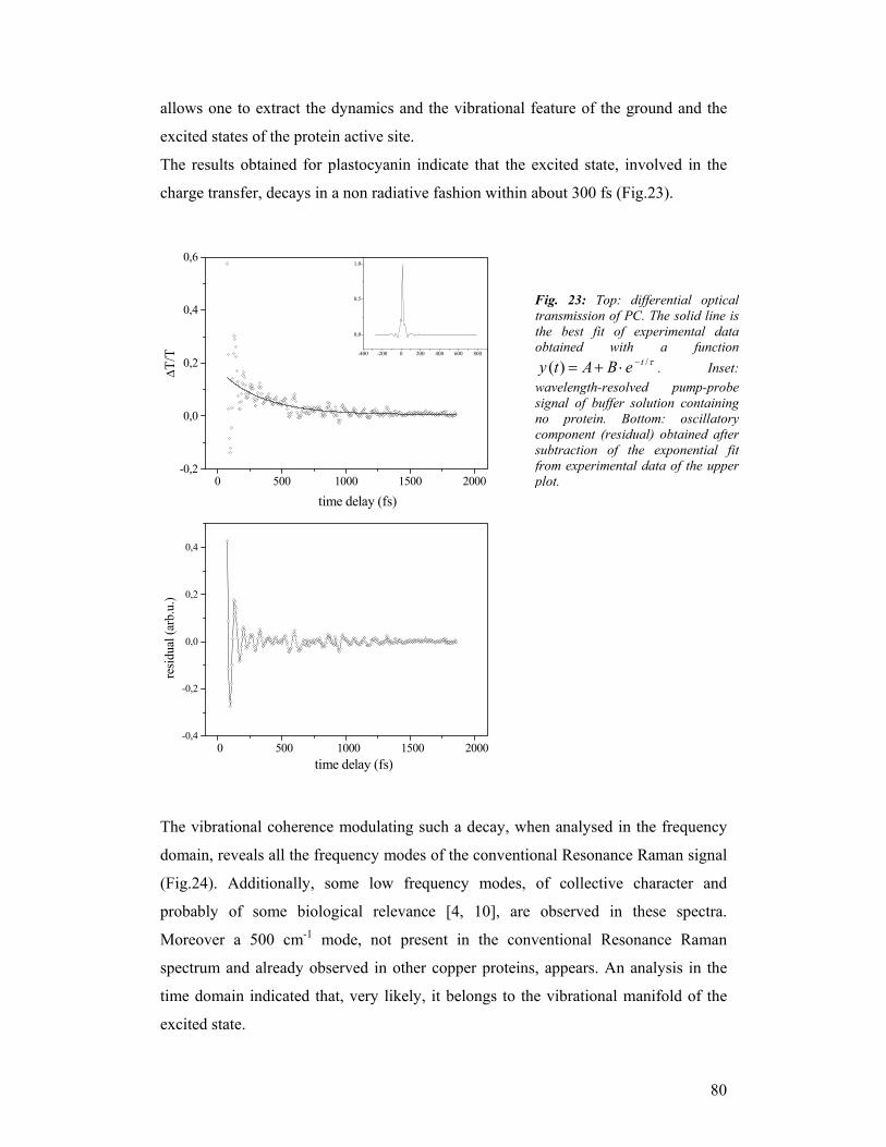
80
allows one to extract the dynamics and the vibrational feature of the ground and the
excited states of the protein active site.
The results obtained for plastocyanin indicate that the excited state, involved in the
charge transfer, decays in a non radiative fashion within about 300 fs (Fig.23).
The vibrational coherence modulating such a decay, when analysed in the frequency
domain, reveals all the frequency modes of the conventional Resonance Raman signal
(Fig.24). Additionally, some low frequency modes, of collective character and
probably of some biological relevance [4, 10], are observed in these spectra.
Moreover a 500 cm-1 mode, not present in the conventional Resonance Raman
spectrum and already observed in other copper proteins, appears. An analysis in the
time domain indicated that, very likely, it belongs to the vibrational manifold of the
excited state.
Fig. 23: Top: differential opticaltransmission of PC. The solid line isthe best fit of experimental dataobtained with a function
τ/)( teBAty −⋅+= . Inset:wavelength-resolved pump-probesignal of buffer solution containingno protein. Bottom: oscillatorycomponent (residual) obtained aftersubtraction of the exponential fitfrom experimental data of the upperplot.
0 500 1000 1500 2000-0,4
-0,2
0,0
0,2
0,4
time delay (fs)
time delay (fs)
resi
dual
(arb
.u.)
0 500 1000 1500 2000-0,2
0,0
0,2
0,4
0,6
∆T/T -400 -200 0 200 400 600 800
0,0
0,5
1,0
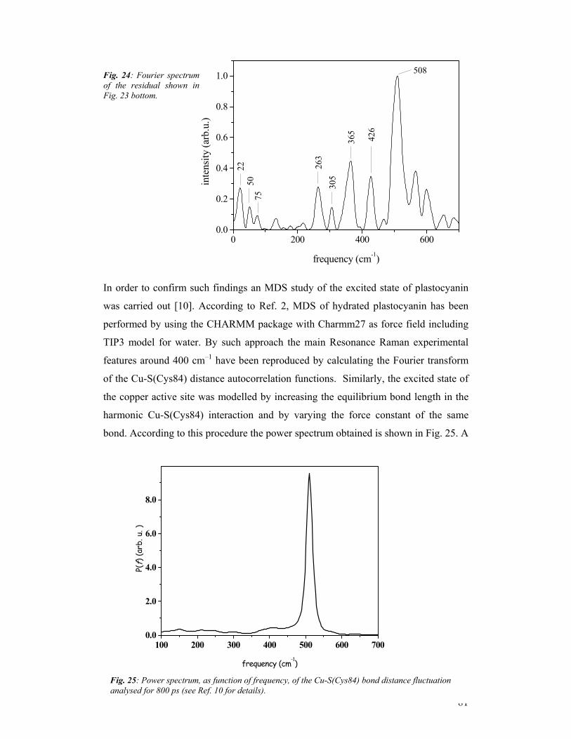
81
In order to confirm such findings an MDS study of the excited state of plastocyanin
was carried out [10]. According to Ref. 2, MDS of hydrated plastocyanin has been
performed by using the CHARMM package with Charmm27 as force field including
TIP3 model for water. By such approach the main Resonance Raman experimental
features around 400 cm–1 have been reproduced by calculating the Fourier transform
of the Cu-S(Cys84) distance autocorrelation functions. Similarly, the excited state of
the copper active site was modelled by increasing the equilibrium bond length in the
harmonic Cu-S(Cys84) interaction and by varying the force constant of the same
bond. According to this procedure the power spectrum obtained is shown in Fig. 25. A
0 200 400 6000.0
0.2
0.4
0.6
0.8
1.0 508
426
365
305
263
7550
22
frequency (cm-1)
inte
nsity
(arb
.u.)
Fig. 24: Fourier spectrumof the residual shown inFig. 23 bottom.
100 200 300 400 500 600 7000.0
2.0
4.0
6.0
8.0
P(f)
(arb
. u. )
frequency (cm-1)
Fig. 25: Power spectrum, as function of frequency, of the Cu-S(Cys84) bond distance fluctuation analysed for 800 ps (see Ref. 10 for details).
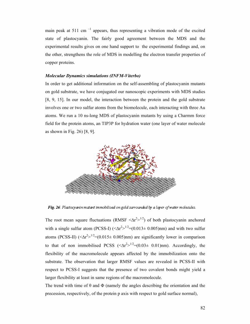
82
main peak at 511 cm –1 appears, thus representing a vibration mode of the excited
state of plastocyanin. The fairly good agreement between the MDS and the
experimental results gives on one hand support to the experimental findings and, on
the other, strengthens the role of MDS in modelling the electron transfer properties of
copper proteins.
Molecular Dynamics simulations (INFM-Viterbo)
In order to get additional information on the self-assembling of plastocyanin mutants
on gold substrate, we have conjugated our nanoscopic experiments with MDS studies
[8, 9, 15]. In our model, the interaction between the protein and the gold substrate
involves one or two sulfur atoms from the biomolecule, each interacting with three Au
atoms. We run a 10 ns-long MDS of plastocyanin mutants by using a Charmm force
field for the protein atoms, an TIP3P for hydration water (one layer of water molecule
as shown in Fig. 26) [8, 9].
The root mean square fluctuations (RMSF <∆r2>1/2) of both plastocyanin anchored
with a single sulfur atom (PCSS-I) (<∆r2>1/2=(0.013± 0.005)nm) and with two sulfur
atoms (PCSS-II) (<∆r2>1/2=(0.015± 0.005)nm) are significantly lower in comparison
to that of non immobilised PCSS (<∆r2>1/2=(0.03± 0.01)nm). Accordingly, the
flexibility of the macromolecule appears affected by the immobilization onto the
substrate. The observation that larger RMSF values are revealed in PCSS-II with
respect to PCSS-I suggests that the presence of two covalent bonds might yield a
larger flexibility at least in same regions of the macromolecule.
The trend with time of θ and Φ (namely the angles describing the orientation and the
precession, respectively, of the protein p axis with respect to gold surface normal),
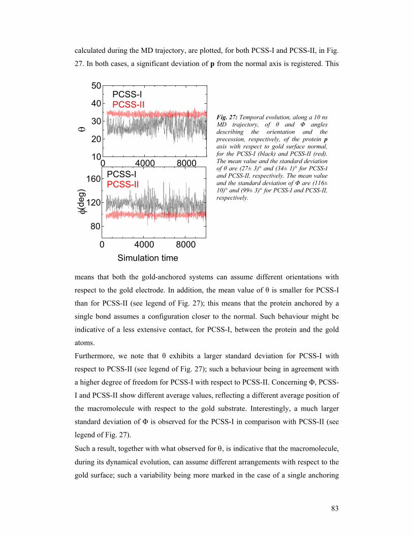
83
calculated during the MD trajectory, are plotted, for both PCSS-I and PCSS-II, in Fig.
27. In both cases, a significant deviation of p from the normal axis is registered. This
means that both the gold-anchored systems can assume different orientations with
respect to the gold electrode. In addition, the mean value of θ is smaller for PCSS-I
than for PCSS-II (see legend of Fig. 27); this means that the protein anchored by a
single bond assumes a configuration closer to the normal. Such behaviour might be
indicative of a less extensive contact, for PCSS-I, between the protein and the gold
atoms.
Furthermore, we note that θ exhibits a larger standard deviation for PCSS-I with
respect to PCSS-II (see legend of Fig. 27); such a behaviour being in agreement with
a higher degree of freedom for PCSS-I with respect to PCSS-II. Concerning Φ, PCSS-
I and PCSS-II show different average values, reflecting a different average position of
the macromolecule with respect to the gold substrate. Interestingly, a much larger
standard deviation of Φ is observed for the PCSS-I in comparison with PCSS-II (see
legend of Fig. 27).
Such a result, together with what observed for θ, is indicative that the macromolecule,
during its dynamical evolution, can assume different arrangements with respect to the
gold surface; such a variability being more marked in the case of a single anchoring
Fig. 27: Temporal evolution, along a 10 nsMD trajectory, of θ and Φ anglesdescribing the orientation and theprecession, respectively, of the protein paxis with respect to gold surface normal,for the PCSS-I (black) and PCSS-II (red).The mean value and the standard deviationof θ are (27± 3)° and (34± 1)° for PCSS-Iand PCSS-II, respectively. The mean valueand the standard deviation of Φ are (116±10)° and (99± 3)° for PCSS-I and PCSS-II,respectively.
0 4000 8000
80 120 160 PCSS-I
PCSS-II
φ (deg
)
Simulation time
0 4000 800010 20 30 40 50
PCSS-I PCSS-II
θ
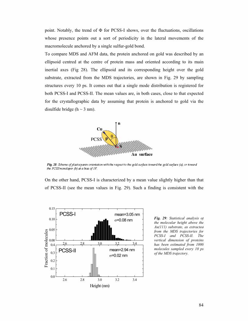
84
point. Notably, the trend of Φ for PCSS-I shows, over the fluctuations, oscillations
whose presence points out a sort of periodicity in the lateral movements of the
macromolecule anchored by a single sulfur-gold bond.
To compare MDS and AFM data, the protein anchored on gold was described by an
ellipsoid centred at the centre of protein mass and oriented according to its main
inertial axes (Fig 28). The ellipsoid and its corresponding height over the gold
substrate, extracted from the MDS trajectories, are shown in Fig. 29 by sampling
structures every 10 ps. It comes out that a single mode distribution is registered for
both PCSS-I and PCSS-II. The mean values are, in both cases, close to that expected
for the crystallographic data by assuming that protein is anchored to gold via the
disulfide bridge (h ~ 3 nm).
On the other hand, PCSS-I is characterized by a mean value slightly higher than that
of PCSS-II (see the mean values in Fig. 29). Such a finding is consistent with the
2.6 2.8 3.0 3.2 3.40.0
0.1
0.2
0.3
0.4mean=2.94 nmσ=0.02 nm
PCSS-II
Frac
tion
of m
olec
ules
Height (nm)
2.6 2.8 3.0 3.2 3.40.00
0.05
0.10
0.15
mean=3.05 nmσ=0.08 nm
PCSS-I
Fig. 29: Statistical analysis ofthe molecular height above theAu(111) substrate, as extractedfrom the MDS trajectories forPCSS-I and PCSS-II. Thevertical dimension of proteinshas been estimated from 1000molecules sampled every 10 psof the MDS trajectory.
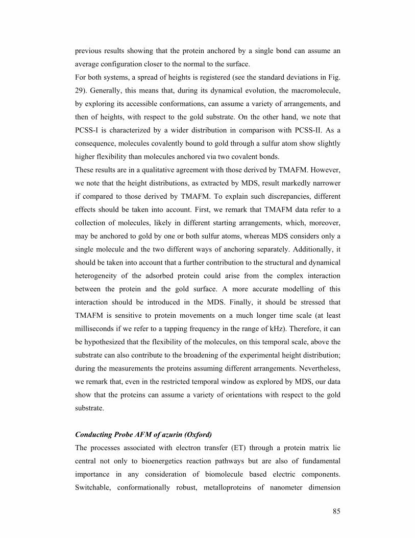
85
previous results showing that the protein anchored by a single bond can assume an
average configuration closer to the normal to the surface.
For both systems, a spread of heights is registered (see the standard deviations in Fig.
29). Generally, this means that, during its dynamical evolution, the macromolecule,
by exploring its accessible conformations, can assume a variety of arrangements, and
then of heights, with respect to the gold substrate. On the other hand, we note that
PCSS-I is characterized by a wider distribution in comparison with PCSS-II. As a
consequence, molecules covalently bound to gold through a sulfur atom show slightly
higher flexibility than molecules anchored via two covalent bonds.
These results are in a qualitative agreement with those derived by TMAFM. However,
we note that the height distributions, as extracted by MDS, result markedly narrower
if compared to those derived by TMAFM. To explain such discrepancies, different
effects should be taken into account. First, we remark that TMAFM data refer to a
collection of molecules, likely in different starting arrangements, which, moreover,
may be anchored to gold by one or both sulfur atoms, whereas MDS considers only a
single molecule and the two different ways of anchoring separately. Additionally, it
should be taken into account that a further contribution to the structural and dynamical
heterogeneity of the adsorbed protein could arise from the complex interaction
between the protein and the gold surface. A more accurate modelling of this
interaction should be introduced in the MDS. Finally, it should be stressed that
TMAFM is sensitive to protein movements on a much longer time scale (at least
milliseconds if we refer to a tapping frequency in the range of kHz). Therefore, it can
be hypothesized that the flexibility of the molecules, on this temporal scale, above the
substrate can also contribute to the broadening of the experimental height distribution;
during the measurements the proteins assuming different arrangements. Nevertheless,
we remark that, even in the restricted temporal window as explored by MDS, our data
show that the proteins can assume a variety of orientations with respect to the gold
substrate.
Conducting Probe AFM of azurin (Oxford)
The processes associated with electron transfer (ET) through a protein matrix lie
central not only to bioenergetics reaction pathways but are also of fundamental
importance in any consideration of biomolecule based electric components.
Switchable, conformationally robust, metalloproteins of nanometer dimension
86
constitute interesting candidates in the integration of biomolecule with molecular-
scale electronic circuitry. In recent years the Oxford team been engaged in a large
program of work in which the transport properties of single molecules and molecular
associations have been analysed within a variety of proximal probe and lithographic
circuitries [11, 16-21]. This report summarises recent progress in conductive probe
AFM based analyses as funded by SAMBA. Specifically, imaging and spectroscopy
have been utilised to investigate electronic properties of a variety of mutants of the
blue copper protein azurin (K27C and zinc K27C) assembled on gold electrode
surfaces under a variety of controllable environmental conditions. Though one can
envisage the use of several methods for investigating the electrical characteristics of
protein/electrode assemblies few, if any, possess the capability of resolving the
contributions of individual molecular components and it is, indeed, these which are of
most relevance to the aim of generating reproducible devices based on single
molecules. Proximal probe analyses can be carried out with exquisite lateral
resolution, with minimal (though tightly controlled) sample preparation, and under a
variety of conditions (ambient, UHV, under fluid). Here we focus on experiments in
which a metallic AFM probe and metallic or semi-metallic substrate constitute source
and drain electrodes. Gold or platinum coated AFM tips can be brought to contact a
molecular monolayer with a controlled contact force. By applying a voltage bias
between the substrate and conducting cantilever, a current flow is generated. Since
one of the key characteristics of biomolecular assemblies is their sensitivity to surface
chemistry, mechanical perturbation and environment, an understanding of the effect
of this sensitivity on transport is required. In consideration of dielectric stability and
mechanical stability we have characterised transport as a function of mechanical
pressure and within this calculated (and simulated) perturbations of tunnel barrier,
resolved the force dependence of dielectric breakdown and calculated molecular
compressibility. An additional principal aim of this project was to investigate the role
of the redox centre in mediating current flow through a single azurin molecule.
Although interesting I-V characteristics for specific junctions have been reported,
understanding of the full spectrum of factors influencing the electrical properties of
metal-molecule-metal junction remains of great interest. Specific mechanisms are, in
many cases, largely unresolved. Examining the dependence of the junction resistance
(or conductance) on presence/absence of redox centre is one approach to examining
the mechanism of transport in potentially switchable configurations.

87
Azurin functions as an electron carrier in the respiratory chain (Pseudomonoas
aeruginosa) and has been characterised in considerable detail. By using a K27C
mutant we are able to control protein-electrode interaction/coupling (and, therefore,
electrochemical switching) through a gold-anchoring cysteine residue onto the surface
of the protein.
Azurin (Pseudomonas aeruginosa azurin wild-type and all surface cysteine mutants)
was kindly supplied by Professor Gerard Canters, Leiden Institute of Chemistry. All
measurements were made using a PicoSPM conducting AFM (Molecular Imaging,
Phoenix) with commercially available Si3N4 tips (tip radius=15±5 nm, Spring
constant=0.12 N/m) coated with Au or Pt. The tips were prepared by soaking in a ca.
5 µM azurin acetate buffer (pH=4.64) for more than 2 hours. Then the modified tip
was brought into contact with a highly oriented pyrolytic graphite (HOPG) substrate.
The schematic of experimental setup was shown in Figure 30.
The bias is applied to HOPG through the electronic circuit, so that the potential could
be expressed as the tip potential vs. substrate. During the acquisition of each current-
voltage (I-V) curve, the force was kept constant and accurately quantified. In order to
study the force dependence of the conductivity associated with the protein structure
distortion, I-V curves at different forces were collected. At every fixed force level, 20
Fig. 30. Schematic of a CP-AFM experimental configuration. The molecule of interest is effectively sandwiched between the electrical contacts formed by a metallic probe and an underlying planar electrode surface.
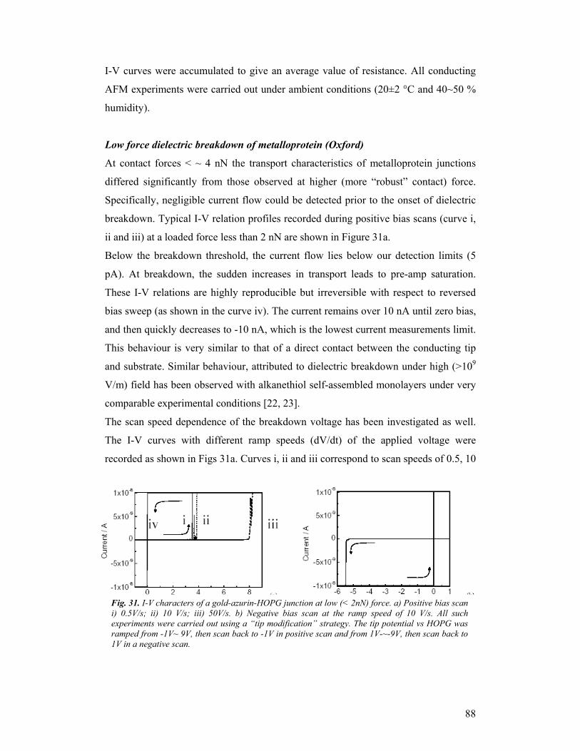
88
I-V curves were accumulated to give an average value of resistance. All conducting
AFM experiments were carried out under ambient conditions (20±2 °C and 40~50 %
humidity).
Low force dielectric breakdown of metalloprotein (Oxford)
At contact forces < ~ 4 nN the transport characteristics of metalloprotein junctions
differed significantly from those observed at higher (more “robust” contact) force.
Specifically, negligible current flow could be detected prior to the onset of dielectric
breakdown. Typical I-V relation profiles recorded during positive bias scans (curve i,
ii and iii) at a loaded force less than 2 nN are shown in Figure 31a.
Below the breakdown threshold, the current flow lies below our detection limits (5
pA). At breakdown, the sudden increases in transport leads to pre-amp saturation.
These I-V relations are highly reproducible but irreversible with respect to reversed
bias sweep (as shown in the curve iv). The current remains over 10 nA until zero bias,
and then quickly decreases to -10 nA, which is the lowest current measurements limit.
This behaviour is very similar to that of a direct contact between the conducting tip
and substrate. Similar behaviour, attributed to dielectric breakdown under high (>109
V/m) field has been observed with alkanethiol self-assembled monolayers under very
comparable experimental conditions [22, 23].
The scan speed dependence of the breakdown voltage has been investigated as well.
The I-V curves with different ramp speeds (dV/dt) of the applied voltage were
recorded as shown in Figs 31a. Curves i, ii and iii correspond to scan speeds of 0.5, 10
Fig. 31. I-V characters of a gold-azurin-HOPG junction at low (< 2nN) force. a) Positive bias scani) 0.5V/s; ii) 10 V/s; iii) 50V/s. b) Negative bias scan at the ramp speed of 10 V/s. All suchexperiments were carried out using a “tip modification” strategy. The tip potential vs HOPG wasramped from -1V~ 9V, then scan back to -1V in positive scan and from 1V-~-9V, then scan back to1V in a negative scan.
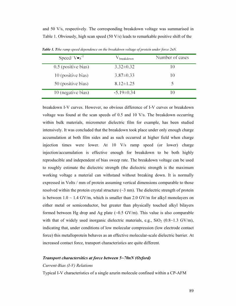
89
and 50 V/s, respectively. The corresponding breakdown voltage was summarised in
Table 1. Obviously, high scan speed (50 V/s) leads to remarkable positive shift of the
breakdown I-V curves. However, no obvious difference of I-V curves or breakdown
voltage was found at the scan speeds of 0.5 and 10 V/s. The breakdown occurring
within bulk materials, micrometer dielectric film for example, has been studied
intensively. It was concluded that the breakdown took place under only enough charge
accumulation at both film sides and as such occurred at higher field when charge
injection times were lower. At 10 V/s ramp speed (or lower) charge
injection/accumulation is effective enough for breakdown to be both highly
reproducible and independent of bias sweep rate. The breakdown voltage can be used
to roughly estimate the dielectric strength (the dielectric strength is the maximum
working voltage a material can withstand without breaking down. It is normally
expressed in Volts / mm of protein assuming vertical dimensions comparable to those
resolved within the protein crystal structure (~3 nm). The dielectric strength of protein
is between 1.0 ~ 1.4 GV/m, which is smaller than 2.0 GV/m for alkyl monolayers on
either metal or semiconductor, but greater than physically touched alkyl bilayers
formed between Hg drop and Ag plate (~0.5 GV/m). This value is also comparable
with that of widely used inorganic dielectric materials, e.g., SiO2 (0.8~1.3 GV/m),
indicating that, under conditions of low molecular compression (low electrode contact
force) this metalloprotein behaves as an effective molecular-scale dielectric barrier. At
increased contact force, transport characteristics are quite different.
Transport charactersitics at force between 5~70nN (Oxford)
Current-Bias (I-V) Relations
Typical I-V characteristics of a single azurin molecule confined within a CP-AFM
Table 1. Tthe ramp speed dependence on the breakdown voltage of protein under force 2nN.
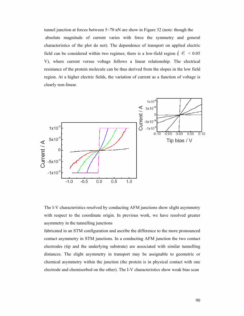
90
tunnel junction at forces between 5~70 nN are show in Figure 32 (note: though the
absolute magnitude of current varies with force the symmetry and general
characteristics of the plot do not). The dependence of transport on applied electric
field can be considered within two regimes; there is a low-field region (V < 0.05
V), where current versus voltage follows a linear relationship. The electrical
resistance of the protein molecule can be thus derived from the slopes in the low field
region. At a higher electric fields, the variation of current as a function of voltage is
clearly non-linear.
The I-V characteristics resolved by conducting AFM junctions show slight asymmetry
with respect to the coordinate origin. In previous work, we have resolved greater
asymmetry in the tunnelling junctions
fabricated in an STM configuration and ascribe the difference to the more pronounced
contact asymmetry in STM junctions. In a conducting AFM junction the two contact
electrodes (tip and the underlying substrate) are associated with similar tunnelling
distances. The slight asymmetry in transport may be assignable to geometric or
chemical asymmetry within the junction (the protein is in physical contact with one
electrode and chemisorbed on the other). The I-V characteristics show weak bias scan
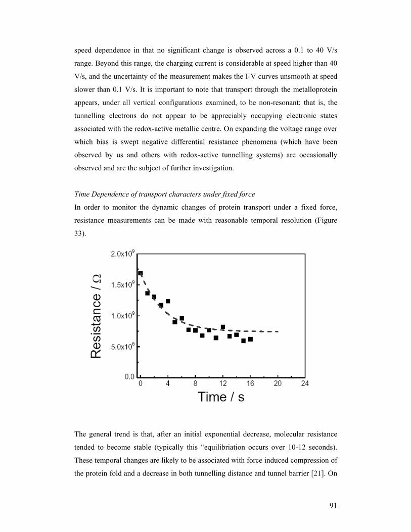
91
speed dependence in that no significant change is observed across a 0.1 to 40 V/s
range. Beyond this range, the charging current is considerable at speed higher than 40
V/s, and the uncertainty of the measurement makes the I-V curves unsmooth at speed
slower than 0.1 V/s. It is important to note that transport through the metalloprotein
appears, under all vertical configurations examined, to be non-resonant; that is, the
tunnelling electrons do not appear to be appreciably occupying electronic states
associated with the redox-active metallic centre. On expanding the voltage range over
which bias is swept negative differential resistance phenomena (which have been
observed by us and others with redox-active tunnelling systems) are occasionally
observed and are the subject of further investigation.
Time Dependence of transport characters under fixed force
In order to monitor the dynamic changes of protein transport under a fixed force,
resistance measurements can be made with reasonable temporal resolution (Figure
33).
The general trend is that, after an initial exponential decrease, molecular resistance
tended to become stable (typically this “equilibriation occurs over 10-12 seconds).
These temporal changes are likely to be associated with force induced compression of
the protein fold and a decrease in both tunnelling distance and tunnel barrier [21]. On
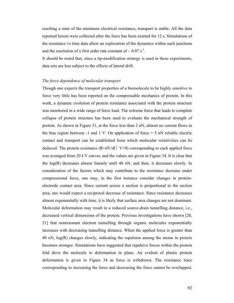
92
reaching a state of the minimum electrical resistance, transport is stable. All the data
reported herein were collected after the force has been exerted for 12 s. Simulations of
the resistance vs time data allow an exploration of the dynamics within such junctions
and the resolution of a first order rate constant of ~ 0.07 s-1.
It should be noted that, since a tip-modification strategy is used in these experiments,
data sets are less subject to the effects of lateral drift.
The force dependence of molecular transport
Though one expects the transport properties of a biomolecule to be highly sensitive to
force very little has been reported on the compressable mechanics of protein. In this
work, a dynamic evolution of protein resistance associated with the protein structure
was monitored in a wide range of force load. The extreme force that leads to complete
collapse of protein structure has been used to evaluate the mechanical strength of
protein. As shown in Figure 31, at the force less than 2 nN, almost no current flows in
the bias region between -1 and 1 V. On application of force > 5 nN reliable electric
contact and transport can be established from which molecular resistivities can be
deduced. The protein resistance (R=dV/dI V=0) corresponding to each applied force
was averaged from 20 I-V curves, and the values are given in Figure 34. It is clear that
the log(R) decreases almost linearly until 40 nN, and then, it decreases slowly. In
consideration of the factors which may contribute to the resistance decrease under
compressional force, one may, in the first instance consider changes in protein-
electrode contact area. Since current across a section is proportional to the section
area, one would expect a reciprocal decrease of resistance. Since resistance decreases
almost exponentially with time, it is likely that surface area changes are not dominant.
Molecular deformation may result in a reduced source-drain tunnelling distance, i.e.,
decreased vertical dimensions of the protein. Previous investigations have shown [20,
21] that nonresonant electron tunnelling through organic molecules exponentially
increases with decreasing tunnelling distance. When the applied force is greater than
40 nN, log(R) changes slowly, indicating the repulsion among the atoms in protein
becomes stronger. Simulations have suggested that repulsive forces within the protein
fold drive the molecule to deformation in plane. An evident of plastic protein
deformation is given in Figure 34 as force is withdrawn. The resistance trace
corresponding to increasing the force and decreasing the force cannot be overlapped.
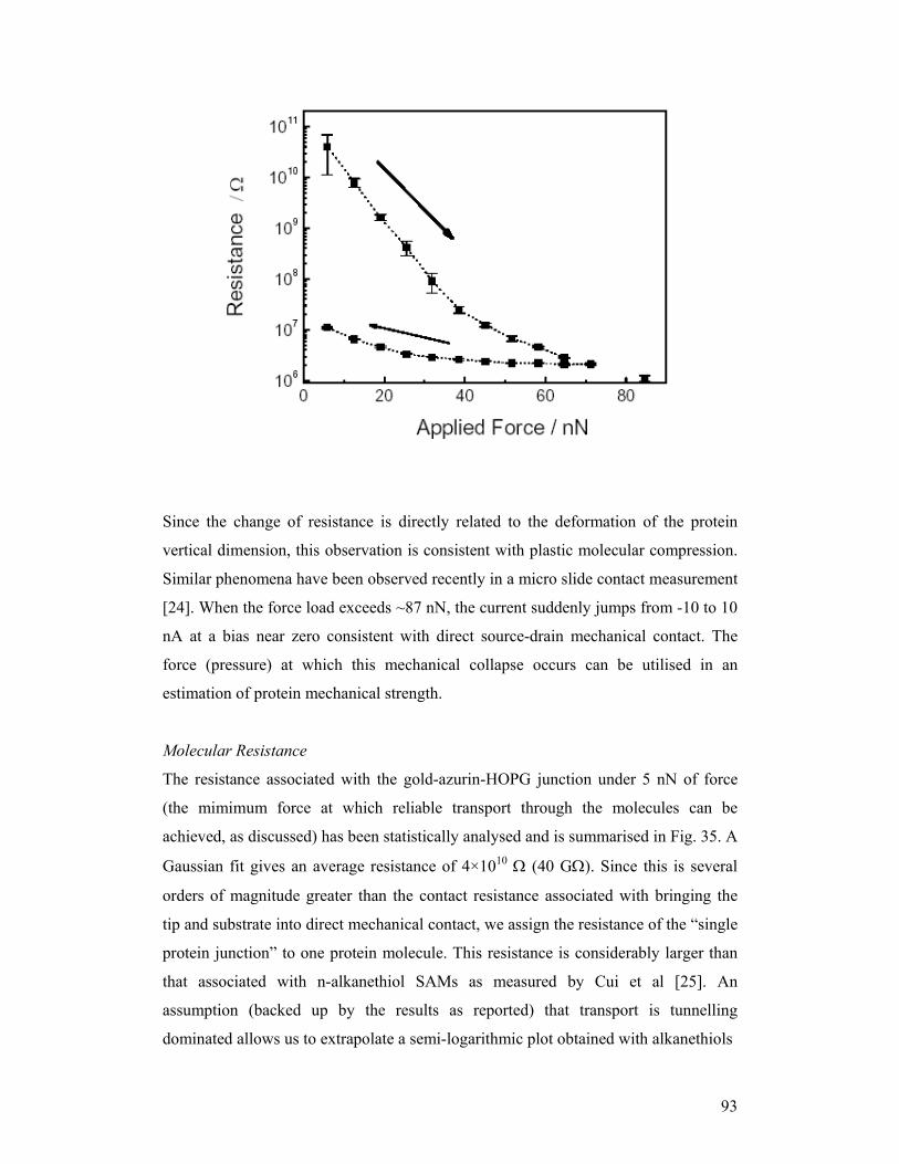
93
Since the change of resistance is directly related to the deformation of the protein
vertical dimension, this observation is consistent with plastic molecular compression.
Similar phenomena have been observed recently in a micro slide contact measurement
[24]. When the force load exceeds ~87 nN, the current suddenly jumps from -10 to 10
nA at a bias near zero consistent with direct source-drain mechanical contact. The
force (pressure) at which this mechanical collapse occurs can be utilised in an
estimation of protein mechanical strength.
Molecular Resistance
The resistance associated with the gold-azurin-HOPG junction under 5 nN of force
(the mimimum force at which reliable transport through the molecules can be
achieved, as discussed) has been statistically analysed and is summarised in Fig. 35. A
Gaussian fit gives an average resistance of 4×10¹⁰ Ω (40 GΩ). Since this is several
orders of magnitude greater than the contact resistance associated with bringing the
tip and substrate into direct mechanical contact, we assign the resistance of the “single
protein junction” to one protein molecule. This resistance is considerably larger than
that associated with n-alkanethiol SAMs as measured by Cui et al [25]. An
assumption (backed up by the results as reported) that transport is tunnelling
dominated allows us to extrapolate a semi-logarithmic plot obtained with alkanethiols
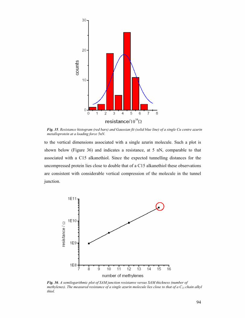
94
to the vertical dimensions associated with a single azurin molecule. Such a plot is
shown below (Figure 36) and indicates a resistance, at 5 nN, comparable to that
associated with a C15 alkanethiol. Since the expected tunnelling distances for the
uncompressed protein lies close to double that of a C15 alkanethiol these observations
are consistent with considerable vertical compression of the molecule in the tunnel
junction.
Fig. 35. Resistance histogram (red bars) and Gaussian fit (solid blue line) of a single Cu centre azurin metalloprotein at a loading force 5nN.
Fig. 36. A semilogarithmic plot of SAM junction resistanve versus SAM thickness (number of methylenes). The measured resistance of a single azurin molecule lies close to that of a C15 chain alkyl thiol.
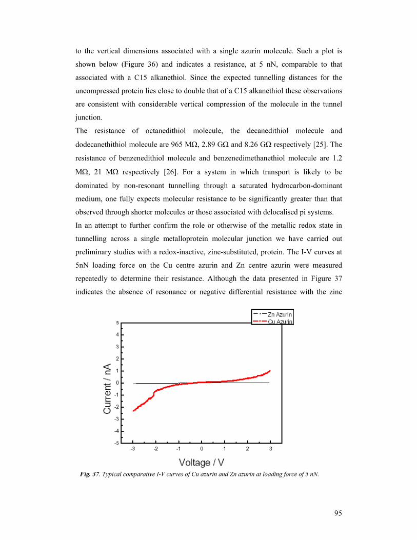
95
to the vertical dimensions associated with a single azurin molecule. Such a plot is
shown below (Figure 36) and indicates a resistance, at 5 nN, comparable to that
associated with a C15 alkanethiol. Since the expected tunnelling distances for the
uncompressed protein lies close to double that of a C15 alkanethiol these observations
are consistent with considerable vertical compression of the molecule in the tunnel
junction.
The resistance of octanedithiol molecule, the decanedithiol molecule and
dodecanethithiol molecule are 965 MΩ, 2.89 GΩ and 8.26 GΩ respectively [25]. The
resistance of benzenedithiol molecule and benzenedimethanethiol molecule are 1.2
MΩ, 21 MΩ respectively [26]. For a system in which transport is likely to be
dominated by non-resonant tunnelling through a saturated hydrocarbon-dominant
medium, one fully expects molecular resistance to be significantly greater than that
observed through shorter molecules or those associated with delocalised pi systems.
In an attempt to further confirm the role or otherwise of the metallic redox state in
tunnelling across a single metalloprotein molecular junction we have carried out
preliminary studies with a redox-inactive, zinc-substituted, protein. The I-V curves at
5nN loading force on the Cu centre azurin and Zn centre azurin were measured
repeatedly to determine their resistance. Although the data presented in Figure 37
indicates the absence of resonance or negative differential resistance with the zinc
Fig. 37. Typical comparative I-V curves of Cu azurin and Zn azurin at loading force of 5 nN.
96
holo protein (even across this large range of bias) a significant number of equivalent
scans with the copper protein are associated with current increase as negative bias.
Though the molecular resistances are comparable at low bias, that associated with the
copper protein drops drastically below that of the zinc protein at larger bias voltages.
The details of this phenomena are currently the subject of more detailed investigation.
Conclusions and future work
In interfacing man-made electronic components with specifically-folded
biomacromolecules, the perturbative effects of junction structure on any signal
generated should be considered. In this study we have established mechanisms by
which the transport properties of single metalloproteins can be characterised.
Specifically, we report herein on the electron transfer characteristics of the blue
copper metalloprotein, azurin, as characterized at a refined level by conducting atomic
force microscopy (CAFM). At low contact forces, the molecules behave as
nanometre-scale dielectrics prior to breakdown at fields in the region of 3~5 V. At
forces > ~ 5 nN reliable electrical contact is achievable from which a detailed study of
molecular resistance as a function of molecular perturbation is possible. Within a low
bias regime, the I-V curve is linear and the molecular resistance can be obtained by
the slope of the I-V curve. The modulation of current-voltage (I-V) behaviour with
compressional force has been examined. In the absence of assignable resonant
electron tunneling within the confined bias region, from -1 to 1 V, the I-V behaviour
has been analysed with a modified Simmons formula. In order to interpret the
variation of tunnelling barrier height and barrier length obtained by fitting with the
modified Simmons formula, an atom packing density model associated with protein
mechanical deformation was proposed and simulated by molecular dynamics. The
barrier heights determined at the minimum forces necessary for stable electrical
contact correlate reasonably well with those estimated from bulk biophysical
(electroanalytical and photochemical) experiments previously reported. At higher
forces, the tunnel barrier decreases to fall within the range observed with saturated
organic systems. The force dependence of the tunnelling distance allowed us further
analyse the stress-strain properties of protein, from which a Young’s modulus of (1.4
± 0.1) ×1010 N/m2 was derived.
Further work will be associated with refining the contributions of different
components of a protein fold to transport and the prospects associated with
97
electrostatic gating of conductance (most relevant to the concept of the “single
metalloprotein transistor”).
Deliverable D3.2: demonstration of a surface assembled enzymic nitrite sensor
(Oxford)
Typical nitrite analyses utilise spectroscopic or potentiometric ion-selective electrode
methodologies [27, 28] though these approaches are either practically slow or suffer
from the effects of interferents, particularly chloride (a problem pertinent to analyses
of waste and drinking water). The utilisation of an enzyme-based detection system has
advantages not only in terms of improved selectivity but is also of value in enhancing
our understanding of the natural electron-transfer processes associated with these
complex macromolecules. Enzymes provide substrate-specific responses to nitrite
with less likelihood of interference from other compounds. The redox activity of the
enzymes can be monitored through the current passed on to the electrode. We report
several approaches to obtain quantifiable nitrite turnover from electroanalyses of the
enzyme nitrite reductase. Analyte presence in the low µM range can be detected from
using either the inorganic compound ruthenium hexamine as an electron mediator or
the natural partner of the enzyme, pseudoazurin.
Experimental
Materials. 1-(3-dimethylaminopropyl)-3-ethyl carbodiimide hydrochloride 98+%,
hexaamineruthenium(III)chloride, 3-mercaptopropionic acid 99+%, and
mercaptosuccinic acid 97% were purchased from Aldrich. Ethanol analytical grade
was obtained from Riedel-DeHaen. Catalase E. C. 1.11.1.6 from bovine liver 30
mg/ml 30,000 units/mg prot was purchased from Sigma. All reagents were of the
highest grade available and used without further purification. Trizma Base and N-
hydroxysuccinimide 98% were obtained from Sigma, aluminium oxide 0.015 µm,
sodium nitrite, sulfuric acid 99%, di-sodium hydrogen orthophosphate 12 hydrate, and
potassium di-hydrogen orthophosphate were from BDH. Ultra pure water (18.2 M.
Elga, UK) was used to make fresh sodium nitrite solutions on a daily basis. The Lys-
Cys-Thr-Cys-Cys-Ala hexapeptide was synthesised by Dr. G. Bloomberg, (University
of Bristol, Department of Biochemistry) using a Pioneer Peptide Synthesiser (Applied
Biosystems) and subsequently purified by HPLC (using a Jupiter RPC18 column) to a
purity of or greater than 95%, and stored at -40oC under argon. Nitrite reductase from
98
Alcaligenes faecalis S-6 was provided by University of Leiden. Reductase
concentrations were determined from adsorbance at 280 nm (ε280 = 46000 M-1 cm-1).
Both proteins were stored at -80 °C in 100 mM phosphate buffer, pH 6.
Voltammetric apparatus and procedure. Electrodes were made of 3 and 4 mm
diameter gold and 9 mm diameter glassy carbon rods cast in epoxy resin as described
elsewhere [29]. Electrodes were polished with 0.015 µm alumina and sonicated in
deionised water before cycling in 1 M sulphuric acid as a systematic cleaning
procedure. A sonic bath SC-52 from Sonicor Instrument Corporation (New York) was
used in this process. Electrochemical measurements were carried out on an Autolab
PGSTAT 12 computer controlled (Dell GX110MT) potentiostat (Eco-Chemie
Utrecht, Netherlands) with a standard three-electrode configuration. The reference and
counter electrodes were a saturated calomel electrode (Radiometer Copenhagen) and
platinum gauze respectively. The contents of the working compartment and solutions
were degassed with high purity (>99.9 %) argon unless stated otherwise. All
potentials are reported with respect to the saturated calomel electrode (SCE), and all
experiments carried out at 22 °C.
Preparation of hexapeptide-modified gold electrode. The surfaces of freshly-cleaned
gold electrodes were modified by cycling +0.7 V vs SCE to –0.7 V vs SCE in the
presence of ~1 mM peptide as described previously [30]. The process of surface
modification is followed both capacitatively and through the progressive inhibition of
diffusive oxygen reduction at the electrode surface.
Electrode modification for direct electrochemistry of nitrite reductase. Freshly
polished 4 mm gold working electrodes were incubated with 3-mercaptopropionic
acid for 1 hour, and sonicated in ethanol. The modified electrodes were incubated for
30 min in a pH 8 phosphate buffer solution of 75 mM 1-(3-dimethylaminopropyl)-3-
ethyl carbodiimide hydrochloride, and 15 mM Nhydroxysuccinimide at 4 °C
according to the method described by Patel et al. [31]. The electrodes were then
rinsed with dionised water and incubated with nitrite reductase overnight.
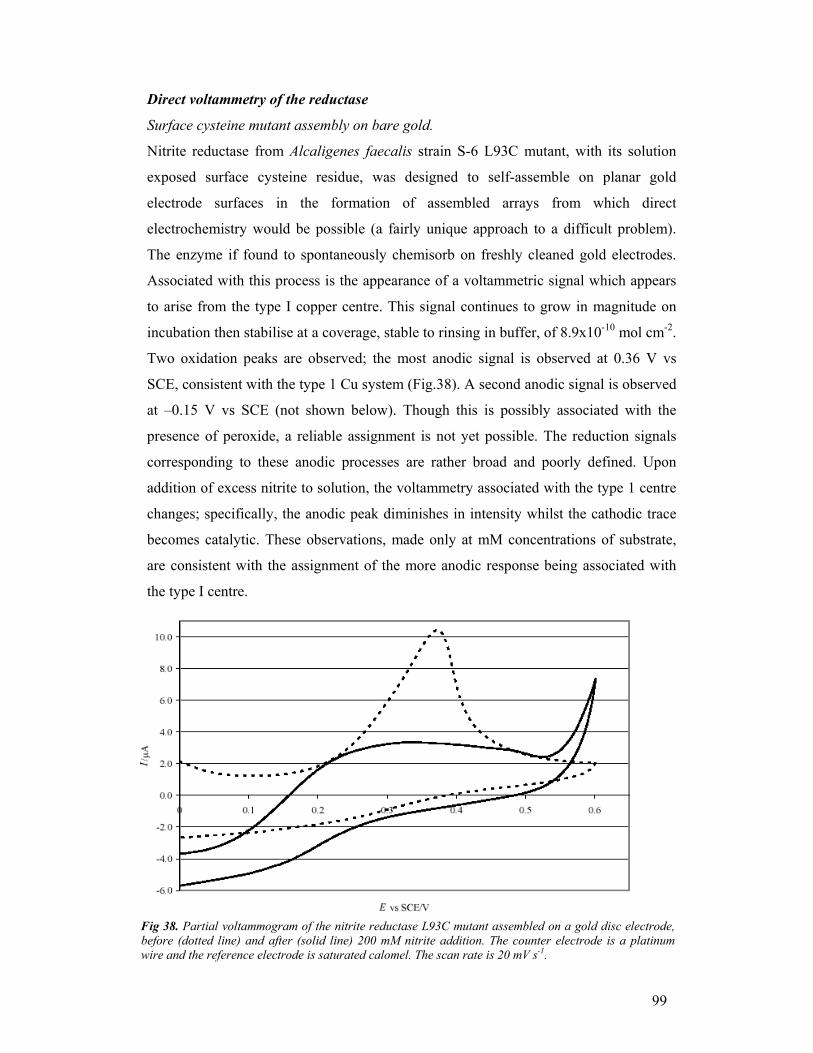
99
Direct voltammetry of the reductase
Surface cysteine mutant assembly on bare gold.
Nitrite reductase from Alcaligenes faecalis strain S-6 L93C mutant, with its solution
exposed surface cysteine residue, was designed to self-assemble on planar gold
electrode surfaces in the formation of assembled arrays from which direct
electrochemistry would be possible (a fairly unique approach to a difficult problem).
The enzyme if found to spontaneously chemisorb on freshly cleaned gold electrodes.
Associated with this process is the appearance of a voltammetric signal which appears
to arise from the type I copper centre. This signal continues to grow in magnitude on
incubation then stabilise at a coverage, stable to rinsing in buffer, of 8.9x10⁻¹⁰ mol cm-2.
Two oxidation peaks are observed; the most anodic signal is observed at 0.36 V vs
SCE, consistent with the type 1 Cu system (Fig.38). A second anodic signal is observed
at –0.15 V vs SCE (not shown below). Though this is possibly associated with the
presence of peroxide, a reliable assignment is not yet possible. The reduction signals
corresponding to these anodic processes are rather broad and poorly defined. Upon
addition of excess nitrite to solution, the voltammetry associated with the type 1 centre
changes; specifically, the anodic peak diminishes in intensity whilst the cathodic trace
becomes catalytic. These observations, made only at mM concentrations of substrate,
are consistent with the assignment of the more anodic response being associated with
the type I centre.
Fig 38. Partial voltammogram of the nitrite reductase L93C mutant assembled on a gold disc electrode, before (dotted line) and after (solid line) 200 mM nitrite addition. The counter electrode is a platinumwire and the reference electrode is saturated calomel. The scan rate is 20 mV s-1.
100
Though reproducible, these responses are stable only over a period of 1-2 hours. We
conclude from this preliminary study that, though the enzyme can be engineered so as
to be conducive to both direct (bare single crystalline gold) surface immobilisation
and direct voltammetry, obtained responses are not sufficiently well defined nor
stable for robust sensor fabrication. More reliable immobilisation and voltammetry
can be obtained through the use of electrode bound self assembled monolayers.
Direct SAM adsorbed voltammetry of nitrite reductase.
Nitrite reductase covalently bound to a 3-mercaptopropionic acid SAM modified gold
undergoes reliable direct electron transfer (20 mV/s, pH 6.0). Under these specific
conditions, the midpoint potential, Em calculated as (Epred + Ep
ox)/2 is 150 mV vs SCE.
In our conditions, the peak-to-peak separation, (∆Ep = Epox - Ep
red), is 100 mV at 100
mV s-1, which is larger than expected for an adsorbed electrochemically reversible
process. However, the magnitude of the ratio of the peak currents (Ipred / Ip
ox) is close
to unity, and ∆Ep remains stable around 100 mV as the scan rate is increased over the
range 20 to 20000 mV s-1, thus allowing a good estimation of the electron transfer
rate constant we were able to plot the peak separation against scan rate and deduce the
electron transfer constant using the Butler-Volmer equation according to the method
described by Jeuken et al. [32]. The potential values are averaged from three sets of
experiments Figure 39. The calculated electron transfer constant is k0 = 9 ± 3 s-1. This
Fig. 39. Trumpet plot showing the peak separation of nitrite reductase covalently attached to 3-mercapto propionic acid modified gold against log of the scan rate, k0 is deduced from the datafitting. From the integration of the peak currents averaged from three different experiments, theprotein density at the electrode surface is 1.23x10⁻¹⁰ mol cm-2 this is compatible with a monolayer ofprotein molecules of 5-6 nm diameter containing 3 detectable redox sites (within the trimer) [40].
101
signal remains unchanged on the addition of nitrite to solution.
Diffusive phase pseudoazurin voltammetry
The diffusive electrochemical response of pseudoazu at a hexapeptide-modified gold
electrode is shown in Figure 40. At a protein concentration of 1 mM, no voltammetric
signal is observed in the absence of the peptide modifier. The diffusive current
response at hexapeptide-modified gold electrode shows an expected linear variance
with square root of scan rate. Faradaic peak separations were reproducibly close to 80
mV at slow scan rates (≤ 100 mV s-1), consistent with a quasi-reversible
electrochemical process. Voltammetric analyses across a pH range of 6-9 were
consistent with minimal (<20 mV per pH unit) dependence. The variance of peak
separation with scan rate can be used to calculate the heterogeneous electron transfer
rate constant according to the formulism of Nicholson and Shain [34]. Within this the
electrochemical rate constant is directly related to ∆Ep in semi reversible
electrochemical systems. The relation is given by equation (1).
0aDks
πγ
ϕα
= (1)
Fig. 40. Cyclic voltammograms obtained from a pH 6.0 phosphate buffer (100 mM) solution of 1 mMpseudoazurin (dotted) in the presence of 500 µM nitrite reductase (grey) and 5 mM nitrite (black), at a 3 mmdiameter peptide modified gold.
102
Where:
rDD0=γ (assumed to be 1) and a = nFv/RT
ϕ is a dimensionless parameter deduced from working curves. D0 is the diffusion
coefficient of the oxidized form and Dr of the reduced form and ks is the
heterogeneous electron transfer rate constant. The transfer coefficient, α, denotes the
position of the transition state associated with electron transfer with respect to the
oxidised and reduced forms, here taken to be 0.5 as the intensity of the reduction and
the oxidation currents are very similar. In all calculations, n is taken to be 1.
The values for ϕ were calculated from the experimental values for ∆Ep, using working
curves [34] (independent of salt concentration over a 20-200 mM range), ks values
were then calculated according to equation 1. By fitting experimental data to working
curves, ks values, calculated through equation 1, were ks = (3.3 ± 0.6) x 10-3 cm s-1.
This value was observed to show some dependence on the quality (determined
voltammetrically) of the peptide layer formed. At varying concentrations of protein,
no peak potential shift was observed (Astier et al. Electroanalysis in press) thus
demonstrating that no protein adsorption is taking place on the adlayer.
Pseudoazurin Interactions with nitrite reductase (“natural partner enzyme
mediation”)
A significant perturbation of the pseudoazurin diffusive voltammetric signal is
observed when nitrite reductase is added, in molar excess (0.5 mM) to the solution
(Fig. 42). Specifically, the quasi-reversible response becomes sigmoidal in appearance
– an observation fully consistent with the occurrence of an electrocatalytic reaction
with the enzyme (though the diffusive half wave potential is perturbed by interactions
with the reductase, the accompanying changes in wave shape make this difficult to
reliably quantify). In solution, both the pseudoazurin and the reductase are able to
adopt relative orientations conducive to the formation of a transient association
complex. In the absence of nitrite, and presence of low levels of dioxygen, it is likely
that these observations are indicative of peroxide generation by the reductase (the
electrocatalytic signal has a smaller peak current intensity when the cell is kept under
argon and diminishes on vigorous degassing). We see a minimum interference by
oxygen on nitrite turnover (within experimental error).
103
One can define the electron transfer steps in this electroanalytical system as follows:
At the electrode:
(i) Pseudoazurin (ox) + e- → Pseudoazurin (red)
The diffusive-phase peak current (Id in amperes) associated with step (i) is given by
the Randles-Sevcik
equation:
Id = 2.69 x 10⁵ n3/2 A C D1/2 v1/2
For fixed values of A (here 0.07 cm2) and C (here 0.5 µM), a plot of Id vs square root
of scan rate allows a direct determination of the protein diffusion coefficient, D, as
(1.13 ± 0.2) x 10-6 cm2 s-1, a value in good agreement with previous determinations
[35].
In the solution:
(ii) Pseudoazurin (red) + NO2- →NiR Pseudoazurin (ox) + NO
Fig. 41. Schematic representation of the hexapeptide-pseudoazurin-NiR system.
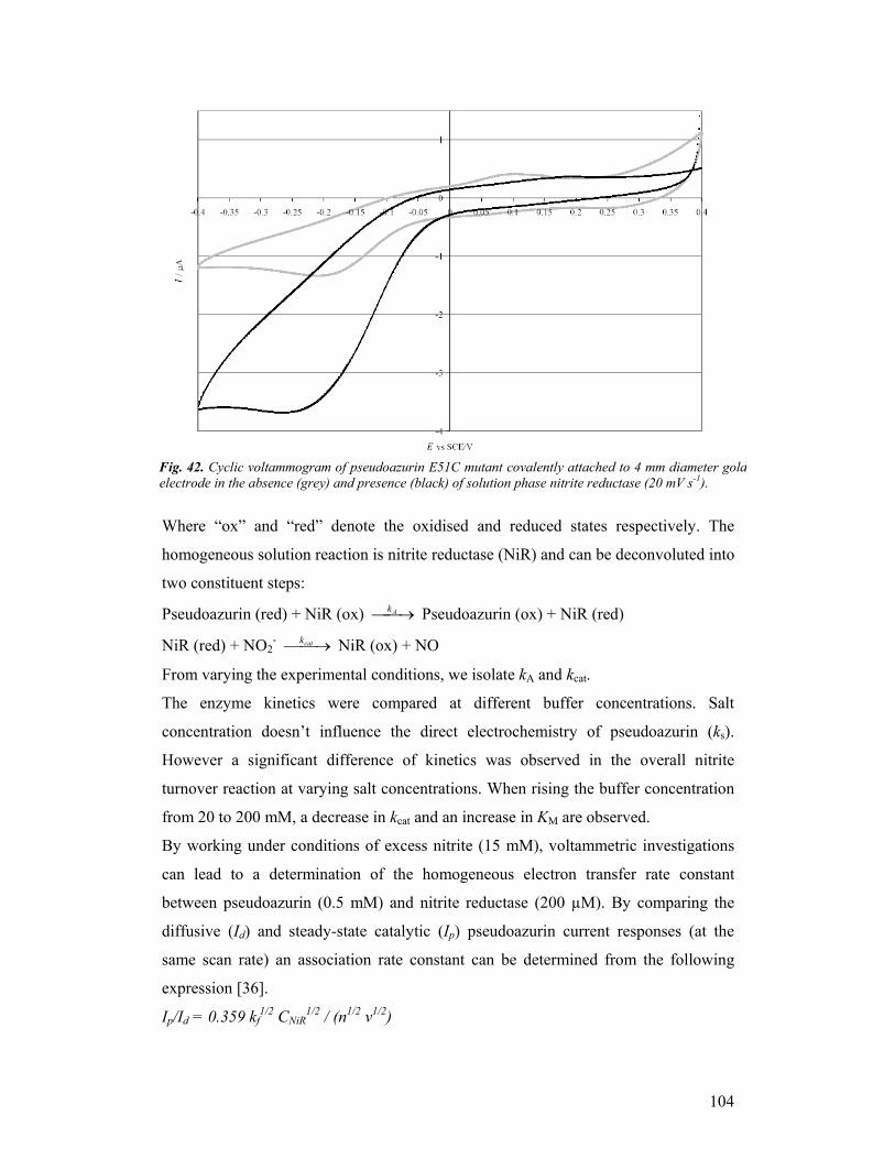
104
Where “ox” and “red” denote the oxidised and reduced states respectively. The
homogeneous solution reaction is nitrite reductase (NiR) and can be deconvoluted into
two constituent steps:
Pseudoazurin (red) + NiR (ox) → Ak Pseudoazurin (ox) + NiR (red)
NiR (red) + NO2- → catk NiR (ox) + NO
From varying the experimental conditions, we isolate kA and kcat.
The enzyme kinetics were compared at different buffer concentrations. Salt
concentration doesn’t influence the direct electrochemistry of pseudoazurin (ks).
However a significant difference of kinetics was observed in the overall nitrite
turnover reaction at varying salt concentrations. When rising the buffer concentration
from 20 to 200 mM, a decrease in kcat and an increase in KM are observed.
By working under conditions of excess nitrite (15 mM), voltammetric investigations
can lead to a determination of the homogeneous electron transfer rate constant
between pseudoazurin (0.5 mM) and nitrite reductase (200 µM). By comparing the
diffusive (Id) and steady-state catalytic (Ip) pseudoazurin current responses (at the
same scan rate) an association rate constant can be determined from the following
expression [36].
Ip/Id = 0.359 kf1/2 CNiR
1/2 / (n1/2 v1/2)
Fig. 42. Cyclic voltammogram of pseudoazurin E51C mutant covalently attached to 4 mm diameter gold electrode in the absence (grey) and presence (black) of solution phase nitrite reductase (20 mV s-1).
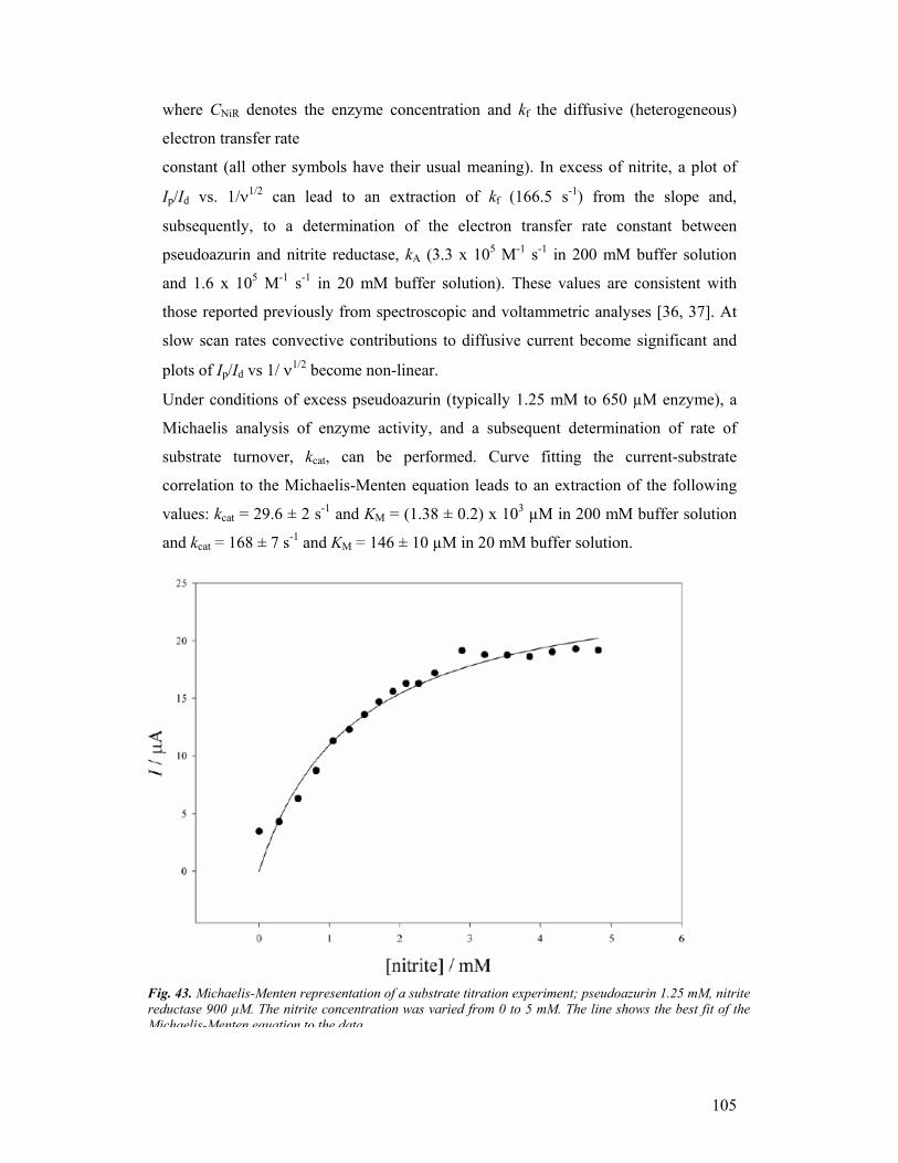
105
where CNiR denotes the enzyme concentration and kf the diffusive (heterogeneous)
electron transfer rate
constant (all other symbols have their usual meaning). In excess of nitrite, a plot of
Ip/Id vs. 1/ν1/2 can lead to an extraction of kf (166.5 s-1) from the slope and,
subsequently, to a determination of the electron transfer rate constant between
pseudoazurin and nitrite reductase, kA (3.3 x 10⁵ M-1 s-1 in 200 mM buffer solution
and 1.6 x 10⁵ M-1 s-1 in 20 mM buffer solution). These values are consistent with
those reported previously from spectroscopic and voltammetric analyses [36, 37]. At
slow scan rates convective contributions to diffusive current become significant and
plots of Ip/Id vs 1/ ν1/2 become non-linear.
Under conditions of excess pseudoazurin (typically 1.25 mM to 650 µM enzyme), a
Michaelis analysis of enzyme activity, and a subsequent determination of rate of
substrate turnover, kcat, can be performed. Curve fitting the current-substrate
correlation to the Michaelis-Menten equation leads to an extraction of the following
values: kcat = 29.6 ± 2 s-1 and KM = (1.38 ± 0.2) x 103 µM in 200 mM buffer solution
and kcat = 168 ± 7 s-1 and KM = 146 ± 10 µM in 20 mM buffer solution.
Fig. 43. Michaelis-Menten representation of a substrate titration experiment; pseudoazurin 1.25 mM, nitritereductase 900 µM. The nitrite concentration was varied from 0 to 5 mM. The line shows the best fit of theMichaelis-Menten equation to the data
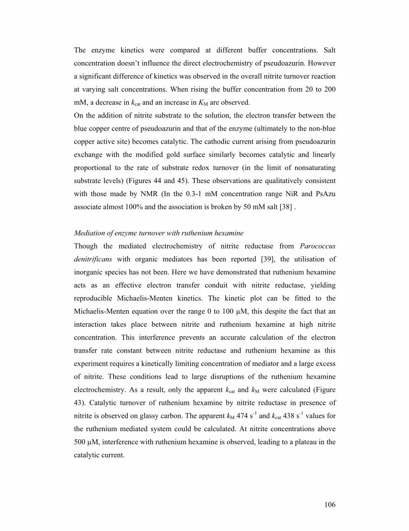
106
The enzyme kinetics were compared at different buffer concentrations. Salt
concentration doesn’t influence the direct electrochemistry of pseudoazurin. However
a significant difference of kinetics was observed in the overall nitrite turnover reaction
at varying salt concentrations. When rising the buffer concentration from 20 to 200
mM, a decrease in kcat and an increase in KM are observed.
On the addition of nitrite substrate to the solution, the electron transfer between the
blue copper centre of pseudoazurin and that of the enzyme (ultimately to the non-blue
copper active site) becomes catalytic. The cathodic current arising from pseudoazurin
exchange with the modified gold surface similarly becomes catalytic and linearly
proportional to the rate of substrate redox turnover (in the limit of nonsaturating
substrate levels) (Figures 44 and 45). These observations are qualitatively consistent
with those made by NMR (In the 0.3-1 mM concentration range NiR and PsAzu
associate almost 100% and the association is broken by 50 mM salt [38] .
Mediation of enzyme turnover with ruthenium hexamine
Though the mediated electrochemistry of nitrite reductase from Parococcus
denitrificans with organic mediators has been reported [39], the utilisation of
inorganic species has not been. Here we have demonstrated that ruthenium hexamine
acts as an effective electron transfer conduit with nitrite reductase, yielding
reproducible Michaelis-Menten kinetics. The kinetic plot can be fitted to the
Michaelis-Menten equation over the range 0 to 100 µM, this despite the fact that an
interaction takes place between nitrite and ruthenium hexamine at high nitrite
concentration. This interference prevents an accurate calculation of the electron
transfer rate constant between nitrite reductase and ruthenium hexamine as this
experiment requires a kinetically limiting concentration of mediator and a large excess
of nitrite. These conditions lead to large disruptions of the ruthenium hexamine
electrochemistry. As a result, only the apparent kcat and kM were calculated (Figure
43). Catalytic turnover of ruthenium hexamine by nitrite reductase in presence of
nitrite is observed on glassy carbon. The apparent kM 474 s-1 and kcat 438 s-1 values for
the ruthenium mediated system could be calculated. At nitrite concentrations above
500 µM, interference with ruthenium hexamine is observed, leading to a plateau in the
catalytic current.
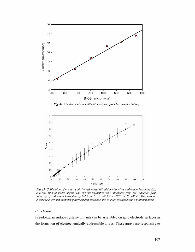
107
Conclusion
Pseudoazurin surface cysteine mutants can be assembled on gold electrode surfaces in
the formation of electrochemically-addressable arrays. These arrays are responsive to
Fig. 44. The linear nitrite calibration regime (pseudoazurin mediation).
Fig 45. Calibration of nitrite by nitrite reductase 400 µM mediated by ruthenium hexamine (III)chloride 10 mM under argon. The current intensities were measured from the reduction peakintensity of ruthenium hexamine cycled from 0.1 to –0.3 V vs SCE at 20 mV s-1. The workingelectrode is a 9 mm diameter glassy carbon electrode, the counter electrode was a platinum mesh.
108
the presence of nitrite reductase and its substrate in solution but electrochemical
coupling is rather weak.
The direct electrochemistry of the enzyme nitrite reductase mutant L93C bound
directly to the gold electrode surface is reported herein. Though electrochemical
signals, responsive to substrate can be obtained, these observations are made only
with difficulty and substrate detection limits are not low. On a hexapeptide modified
gold electrode the diffusional redox signal of wild-type form of pseudoazurin can be
reliably obtained and effectively coupled to substrate turnover by the enzyme in
solution (this configuration effectively constitutes a natural partner electron transfer
relay). Under such circumstances, a calibration of nitrite in the 100 µM range can be
obtained (a level relevant to both food and water treatment industries). The electron
transfer rate constants can be calculated from the electrode to pseudoazurin,
pseudoazurin to nitrite reductase, and an apparent kM and kcat can be calculated.
The enzyme is also effectively “coupled” to an electrode through the use of an
inorganic mediator; under these conditions calibrated nitrite sensing down to 1 µM
levels is achievable. We additionally highlight the influence of the salt concentration
on the electron transfer kinetics between pseudoazurin and nitrite reductase.
References
1. M. Milani, L. Andolfi, S. Cannistraro, M. Ph. Verbeet, M. Bolognesi, Acta
Cryst. D57 (2001) 1735.
2. A.R. Bizzarri, S. Cannistraro, Chem.Phys.Lett. 349 (2001) 503.
3. P. Facci, D. Alliata, S. Cannistraro, Ultramicroscopy 89 (2001) 291.
4. T. Cimei, A.R. Bizzarri, S. Cannistraro, G. Cerullo, S. De Silvestri,
Chem.Phys.Lett. 362 (2002) 497.
5. L. Andolfi, S. Cannistraro, G.W. Canters, P. Facci, A.G. Ficca, I.M.C. Van
Amsterdam and M.Ph. Verbeet, Arch. Biochem. Biophys. 399 (2002) 81.
6. A.R. Bizzarri, S. Cannistraro, Appl. Spectrosc. 56 (2002) 1531.
7. L.Andolfi, B.Bonanni, G.W.Canters, M.Ph. Verbeet, S. Cannistraro, Surface
Science 530 (2003) 181.
8. A.R. Bizzarri, B. Bonanni, G. Costantini, S. Cannistraro, Chem.Phys.Chem. 4
(2003) 1189-1195.
109
9. A.R. Bizzarri, G. Costantini, S. Cannistraro, Biophys.Chem. 4 (2003) 1189-
1195.
10. T. Cimei, A.R. Bizzarri, G. Cerullo, S. De Silvestri, S. Cannistraro, Biophys.
Chem. 106 (2003) 221-231.
11. L. Andolfi, D. Bruce, S. Cannistraro, G.W. Canters, J.J. Davis, H.A.O. Hill, J.
Crozier, M. Ph. Verbeet, C.W. Wrathmell, Y. Astier, J. Electroanal. Chem. 565
(2004) 21-28.
12. L. Andolfi, G.W. Canters, M.Ph. Verbeet, S. Cannistraro, Biophys. Chem. 107
(2004) 107-116.
13. D. Alliata, L. Andolfi, S. Cannistraro, Ultramicroscopy (2004) submitted.
14. L. Andolfi, D.Alliata, S. Cannistraro, Chem. Phys. Chem. (2004) submitted.
15. B. Bonanni, D. Alliata, L. Andolfi, A. R. Bizzarri, S. Cannistraro, Progress in
Surface Science Research (2004) in press.
16. J.J. Davis, Phil. Trans. Royal Soc. A, 2003, 361 (1813) 2807-2825 (Invited Article).
17. J. Zhao, J.J. Davis, Nanotechnology, 2003, 14, 9, 1023-1028.
18. J.J. Davis, IEE Nanobiotechnology 2004, in press.
19. J. Zhao, J.J. Davis, Colloids and Surfaces, (2004) in press.
20. C.L. Wrathmell, J. Zhao, J. Fletcher, D. Djuricic, J.J. Davis, H.A.O. Hill, J.
Molecular Recognition, 2004, 17, 1-7.
21. Jianwei Zhao, Jason J. Davis, Mark S. P. Sansom, Andrew Hung, J. Am. Chem.
Soc. 2004, 126, 5601-5609.
22. Wold, D.J. and C.D. Frisbie, J. Am. Chem. Soc. 2001. 123 (23): 5549-5556.
23. Zhao, J.W. and K. Uosaki, Applied Physics Letters, 2003. 83 (10): 2034-2036.
24. Singh-Zocchi, M., J. Hanne, and G. Zocchi, Biophysical Journal, 2002. 83 (4):
2211-2218.
25. Cui, X.D., et al., Journal of Physical Chemistry B, 2002. 106 (34): 8609-8614.
26. Xiao, X.Y., B.Q. Xu, and N.J. Tao, Nano Letters, 2004. 4 (2): 267-271.
27. R. Perez-Olmos, Anal. Science, 1998. 14 (5): 1001-1003.
28. D.J.D. Nicholas, A. Nason, Methods in Enzymology, 1957. 3: 982.
29. L.J.C. Jeuken, J.P. McEvoy, F.A. Armstrong, J. Phys. Chem, 2002. Sect. B 106
(9): 2304-2313.
30. J. Kazlauskaite, et al., Eur. J. Biochem., 1996. 241: 552-556.
31. N. Patel, et al., Langmuir, 1997. 13 (24): 6485-6490.
32. L.J.C. Jeuken, et al., J. Am. Chem. Soc, 2002. 124 (20): 5702-5713.
110
33. M.E. Murphy, S. Turley, E.T. Adman, J. Biol. Chem, 1997. 272: 28455.
34. R. Nicholson, I. Shain, Anal. Chem., 1964. 36 (4): 706-723.
35. T. Kohzuma, et al., J. Biol. Chem.1995. 270: 25733 - 25738.
36. K. Kataoka, et al., J. Inorg. Biochem., 2000. 82: 79-84.
37. T. Kohzuma, et al., Chem. Lett., 1993. 12: 2029-2032.
38. G.W. Canters, unpublished observations.
39. B. Strehlitz, et al., Anal. Chem. 1996. 68: 807-816.
40. L.M. Murphy, et al., J. Mol. Biol. 2002. 315 (4): 859-871.
41. M. Kukimoto, Protein Eng, 1995. 8 (2): 153-158.
110
3.4 WP4
3.4.1 Completion of M13: modeling the coupling between molecule (copper atom) and the metallic nanogate.
The systems of interest for this project are very complex, and involve the
interaction among several objects with different properties, such as proteins, solid
substrates, metallic nanoelectrodes. To cope with such a complexity, we adopted in
our theoretical investigation a basic principle that can be phrased as “multi-level
modeling”.
(i) The first level of modeling operates according to a global point of view and
consists in considering the whole system as composed of simplified objects.
Each individual component is characterized by the intrinsic properties that are
important for the phenomenon under study and that can be estimated to several
degrees of accuracy. The accuracy with which such properties are known affects
the computed quantities: however, several theoretical aspects of the problem can
be unraveled independently of it, and the method to compute such properties
does not need to be specified at this level of modeling. An example of this
approach is the Marcus theory for electron transfer (ET): it gives the desired
quantity (ET rate) in terms of microscopic quantities such as the reorganization
energy and the transfer integrals, whose calculation is not directly part of theory.
(ii) The deeper second level of modeling consists in using computational
methodologies to calculate the properties required in the first-level modeling.
For example, the reorganization energies and transfer integrals that enter the
Marcus theory can be computed by quantum-mechanical methodologies.
The specific problem of the electronic transport through a single molecule connected
to two nanoelectrodes in an ElectroChemical (EC)STM setup was already treated in
the scientific literature, yielding different proposals of first-level models (with the
meaning defined above). Briefly, the advanced interpretations may be summarized in
the three following categories. (a) Two-step sequential ET [1]: in the first step the
electron passes from one electrode, say the substrate, to the oxidized protein, which
has time to fully relax; in the second step the electron moves from the protein to the
other electrode, say the tip. (b) Vibrationally coherent ET [2]: after the first ET from
an electrode to the protein, the second ET (from the protein to the other electrode) is
fast enough that the protein does not have the time to fully relax. (c) Resonant
tunneling [3]: the two ETs from one electrode to the protein and from the protein to
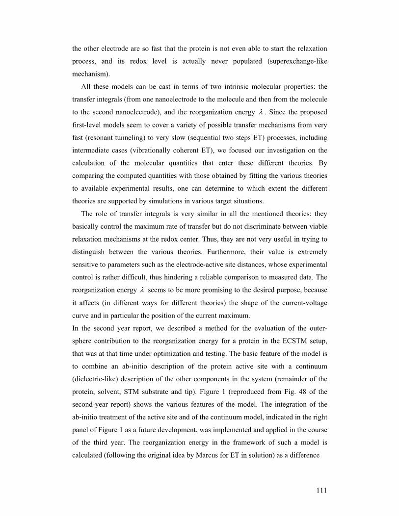
111
the other electrode are so fast that the protein is not even able to start the relaxation
process, and its redox level is actually never populated (superexchange-like
mechanism).
All these models can be cast in terms of two intrinsic molecular properties: the
transfer integrals (from one nanoelectrode to the molecule and then from the molecule
to the second nanoelectrode), and the reorganization energy λ . Since the proposed
first-level models seem to cover a variety of possible transfer mechanisms from very
fast (resonant tunneling) to very slow (sequential two steps ET) processes, including
intermediate cases (vibrationally coherent ET), we focused our investigation on the
calculation of the molecular quantities that enter these different theories. By
comparing the computed quantities with those obtained by fitting the various theories
to available experimental results, one can determine to which extent the different
theories are supported by simulations in various target situations.
The role of transfer integrals is very similar in all the mentioned theories: they
basically control the maximum rate of transfer but do not discriminate between viable
relaxation mechanisms at the redox center. Thus, they are not very useful in trying to
distinguish between the various theories. Furthermore, their value is extremely
sensitive to parameters such as the electrode-active site distances, whose experimental
control is rather difficult, thus hindering a reliable comparison to measured data. The
reorganization energy λ seems to be more promising to the desired purpose, because
it affects (in different ways for different theories) the shape of the current-voltage
curve and in particular the position of the current maximum.
In the second year report, we described a method for the evaluation of the outer-
sphere contribution to the reorganization energy for a protein in the ECSTM setup,
that was at that time under optimization and testing. The basic feature of the model is
to combine an ab-initio description of the protein active site with a continuum
(dielectric-like) description of the other components in the system (remainder of the
protein, solvent, STM substrate and tip). Figure 1 (reproduced from Fig. 48 of the
second-year report) shows the various features of the model. The integration of the
ab-initio treatment of the active site and of the continuum model, indicated in the right
panel of Figure 1 as a future development, was implemented and applied in the course
of the third year. The reorganization energy in the framework of such a model is
calculated (following the original idea by Marcus for ET in solution) as a difference
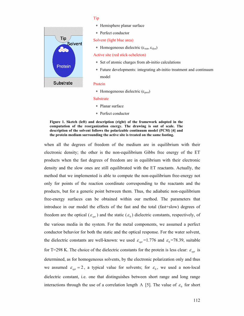
112
when all the degrees of freedom of the medium are in equilibrium with their
electronic density; the other is the non-equilibrium Gibbs free energy of the ET
products when the fast degrees of freedom are in equilibrium with their electronic
density and the slow ones are still equilibrated with the ET reactants. Actually, the
method that we implemented is able to compute the non-equilibrium free-energy not
only for points of the reaction coordinate corresponding to the reactants and the
products, but for a generic point between them. Thus, the adiabatic non-equilibrium
free-energy surfaces can be obtained within our method. The parameters that
introduce in our model the effects of the fast and the total (fast+slow) degrees of
freedom are the optical ( optε ) and the static ( 0ε ) dielectric constants, respectively, of
the various media in the system. For the metal components, we assumed a perfect
conductor behavior for both the static and the optical response. For the water solvent,
the dielectric constants are well-known: we used optε =1.776 and 0ε =78.39, suitable
for T=298 K. The choice of the dielectric constants for the protein is less clear: optε is
determined, as for homogeneous solvents, by the electronic polarization only and thus
we assumed 2optε = , a typical value for solvents; for 0ε , we used a non-local
dielectric constant, i.e. one that distinguishes between short range and long range
interactions through the use of a correlation length Λ [5]. The value of 0ε for short
Tip
∗ Hemisphere planar surface
∗ Perfect conductor
Solvent (light blue area)
∗ Homogeneous dielectric (εstat, εdyn)
Active site (red stick-scheleton)
∗ Set of atomic charges from ab-initio calculations
∗ Future developments: integrating ab-initio treatment and continuum
model
Protein
∗ Homogeneous dielectric (εprot)
Substrate
∗ Planar surface
∗ Perfect conductor
Pperfect conductor
Figure 1. Sketch (left) and description (right) of the framework adopted in thecomputation of the reorganization energy. The drawing is out of scale. Thedescription of the solvent follows the polarizable continuum model (PCM) [4] andthe protein medium surrounding the active site is treated on the same footing.
113
range interactions was chosen equal to optε (they are both determined by the same
electronic polarization), while for long range interactions we chose a value suitable
for a moderately polar environment, 20. The correlation length Λ was assumed equal
to 5 Å. These choices, based on physical common sense, give free-energies in the
same range of those obtained with local constant values of 3-5, that are often used for
proteins. Nevertheless, since we do not have a direct source (experimental or
theoretical) to check the chosen 0ε , before studying the reorganization energy in the
specific ECSTM setup adopted by the experimental INFM group in Modena (P. Facci
and coworkers), we compared λ computed with our model for the azurin electron
self-exchange (ESE) reaction in solution:
Az(II) + Az(I) → Az(I) + Az(II)
with the experimental estimate by Gray et al. [6], who found 0 6 0 8λ = . − . eV. Since
our model described above gives only the outer contribution outλ to λ (due to the
protein outside the active site and the solvent), to compare with experimental results
we also took into account an independent estimate of the inner term inλ . Olsson and
Ryde [7] estimated inλ by means of a QM/MM simulation of azurin, and we used
their value inλ =0.291 eV. The computed value for the total λ is 0.65 eV, in good
agreement with the experiment. Notably, this value was obtained by considering the
two azurin molecules linked by their hydrophobic patch (see Fig.2).
Figure 2. Encounter complex geometry (taken to be equal to the dimer geometry in the crystal)
used in the calculation of λ for the ESE reaction of Az. The dielectric modeling the protein is
represented in blue, the cavities that host the active sites are red.
114
We found that λ is very sensitive to the relative positions of the two proteins in
the encounter complex: in fact, when the two active sites are close enough (as in the
ESE encounter complex), the oxidized site can interact with the medium polarization
which is due to the other (reduced) site, and vice-versa. Thus, the ET reactants feel
before the ET a polarization which is already partly adapted to the ET products. In
other words, the presence of this medium polarization, that exists prior to charge
transfer, quenches the extent of the required structural reorganization, thus decreasing
the reorganization energy. The importance of the spatial proximity between active
sites to have effective protein-protein ET was often related with the need for high
electronic coupling: however, our findings show that the relative spatial arrangement
not only affects the electronic coupling (transfer integral), but is also fundamental for
diminishing the ET reorganization energy and consequently incrementing the transfer
rate.
After this preliminary calculation that allowed us to check the quality of the protein
permittivity parameters in the ESE calculations, we applied our method to the
ECSTM system. Here the ET reaction to be considered is
Az(II) + Electrode → Az(I) + Electrode
where Electrode can be the tip or the substrate. Note that, differently from the ESE,
only one Az molecule takes part in the ET reaction. Thus, one would expect a value of
λ equal to 0.65/2 eV = 0.33 eV if the variation of environmental conditions had a
small/negligible role. By considering an azurin molecule standing with the
Cys3/Cys26 disulfide bridge on the substrate (with the protein major axis
perpendicular to the substrate surface) and the tip (radius=5 nm) standing 5 Å from
the protein surface, we instead obtained a larger value of 0.43 eV. This result depends
on two opposing effects: (i) on one hand, the presence of the ECSTM apparatus
removes water from the protein neighborhood, decreasing λ ; (ii) on the other hand,
the effectiveness of the spatial proximity between the two active centers of the
encounter complex in decreasing λ , is canceled in the ECSTM setup. In the present
case, the latter effect prevails on the former.
We tried to give a lower-bound estimate to λ for Az in the ECSTM setup. To this
end, we considered the protein lying with its major axis parallel to the substrate, with
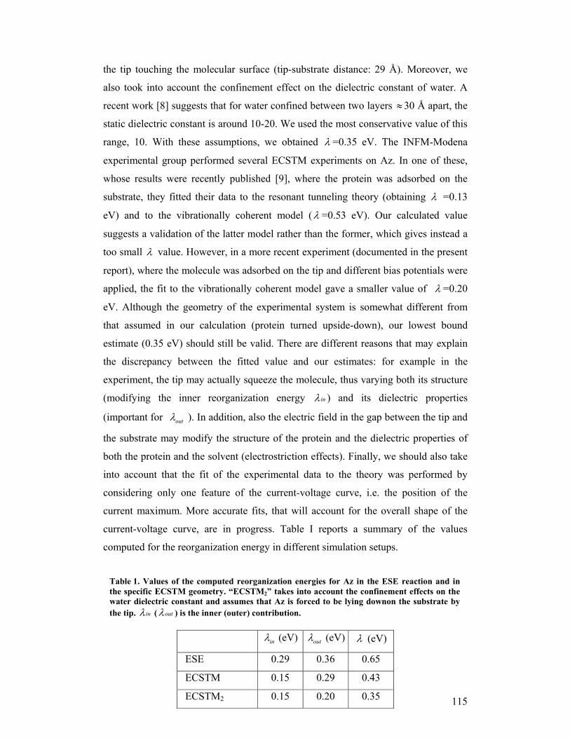
115
the tip touching the molecular surface (tip-substrate distance: 29 Å). Moreover, we
also took into account the confinement effect on the dielectric constant of water. A
recent work [8] suggests that for water confined between two layers ≈ 30 Å apart, the
static dielectric constant is around 10-20. We used the most conservative value of this
range, 10. With these assumptions, we obtained λ =0.35 eV. The INFM-Modena
experimental group performed several ECSTM experiments on Az. In one of these,
whose results were recently published [9], where the protein was adsorbed on the
substrate, they fitted their data to the resonant tunneling theory (obtaining λ =0.13
eV) and to the vibrationally coherent model ( λ =0.53 eV). Our calculated value
suggests a validation of the latter model rather than the former, which gives instead a
too small λ value. However, in a more recent experiment (documented in the present
report), where the molecule was adsorbed on the tip and different bias potentials were
applied, the fit to the vibrationally coherent model gave a smaller value of λ =0.20
eV. Although the geometry of the experimental system is somewhat different from
that assumed in our calculation (protein turned upside-down), our lowest bound
estimate (0.35 eV) should still be valid. There are different reasons that may explain
the discrepancy between the fitted value and our estimates: for example in the
experiment, the tip may actually squeeze the molecule, thus varying both its structure
(modifying the inner reorganization energy inλ ) and its dielectric properties
(important for outλ ). In addition, also the electric field in the gap between the tip and
the substrate may modify the structure of the protein and the dielectric properties of
both the protein and the solvent (electrostriction effects). Finally, we should also take
into account that the fit of the experimental data to the theory was performed by
considering only one feature of the current-voltage curve, i.e. the position of the
current maximum. More accurate fits, that will account for the overall shape of the
current-voltage curve, are in progress. Table I reports a summary of the values
computed for the reorganization energy in different simulation setups.
inλ (eV) outλ (eV) λ (eV)
ESE 0.29 0.36 0.65
ECSTM 0.15 0.29 0.43
ECSTM2 0.15 0.20 0.35
Table 1. Values of the computed reorganization energies for Az in the ESE reaction and inthe specific ECSTM geometry. “ECSTM2” takes into account the confinement effects on thewater dielectric constant and assumes that Az is forced to be lying downon the substrate bythe tip. inλ ( outλ ) is the inner (outer) contribution.
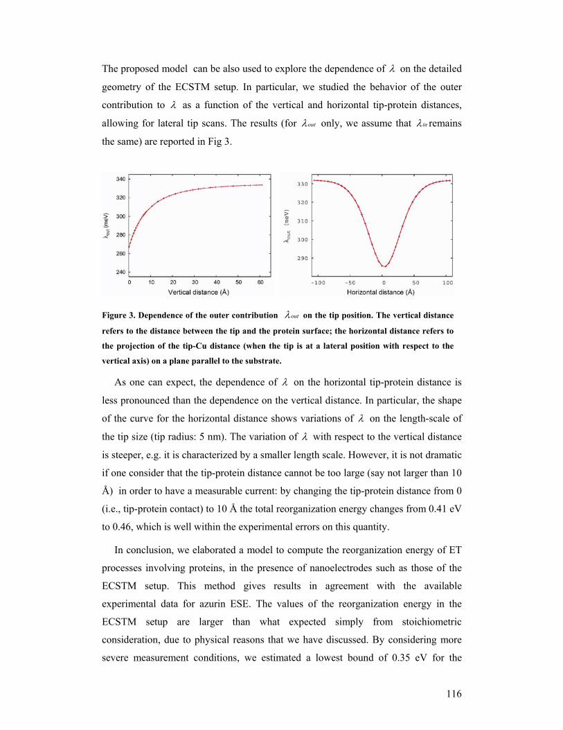
116
The proposed model can be also used to explore the dependence of λ on the detailed
geometry of the ECSTM setup. In particular, we studied the behavior of the outer
contribution to λ as a function of the vertical and horizontal tip-protein distances,
allowing for lateral tip scans. The results (for outλ only, we assume that inλ remains
the same) are reported in Fig 3.
Figure 3. Dependence of the outer contribution outλ on the tip position. The vertical distance
refers to the distance between the tip and the protein surface; the horizontal distance refers to
the projection of the tip-Cu distance (when the tip is at a lateral position with respect to the
vertical axis) on a plane parallel to the substrate.
As one can expect, the dependence of λ on the horizontal tip-protein distance is
less pronounced than the dependence on the vertical distance. In particular, the shape
of the curve for the horizontal distance shows variations of λ on the length-scale of
the tip size (tip radius: 5 nm). The variation of λ with respect to the vertical distance
is steeper, e.g. it is characterized by a smaller length scale. However, it is not dramatic
if one consider that the tip-protein distance cannot be too large (say not larger than 10
Å) in order to have a measurable current: by changing the tip-protein distance from 0
(i.e., tip-protein contact) to 10 Å the total reorganization energy changes from 0.41 eV
to 0.46, which is well within the experimental errors on this quantity.
In conclusion, we elaborated a model to compute the reorganization energy of ET
processes involving proteins, in the presence of nanoelectrodes such as those of the
ECSTM setup. This method gives results in agreement with the available
experimental data for azurin ESE. The values of the reorganization energy in the
ECSTM setup are larger than what expected simply from stoichiometric
consideration, due to physical reasons that we have discussed. By considering more
severe measurement conditions, we estimated a lowest bound of 0.35 eV for the
117
reorganization energy of azurin in the ECSTM setup. The model has been also used to
explore the dependence of λ on the detailed geometry of the system. The method can
also be extended to different experimental setups, including the transistor geometry:
preliminary simulations of a model transistor show its reliability and are promising to
foster further combined theoretical-experimental investigations. Indeed, the novel
methodological implementation and the establishment of such a combined research
activity among different groups was an important added value of this project and
represents its fall-out into the near future.
Finally, we wish to mention another relevant theoretical simulation that is currently
ongoing and that was possible thanks to the methodological achievements and
computational successes described above. For one of the dimerized structures
proposed by the Leiden chemical synthesis group [10], in which two mutated azurins
are connected to each other by means of two water molecules around the Cu centers
and through a chemical linker far from them, we are computing the reorganization
energy and the transfer integrals. The latters are obtained through an ab-initio method
recently implemented in our group [11]. The reorganization energy and the transfer
integrals will then be combined for an evaluation of the experimental observable
which is the transfer rate. The advantage of employing for this study the atomic model
proposed by Canters and coworkers rather than the encounter complex of Figure 2 is
that the presence of a chemical linker between the two molecules of the dimer allows
for kinetic experiments to measure the transfer rate: therefore, we will have a direct
comparison to consistent measured data. This is another example of activity that was
stimulated in the course of this project and was made possible by the
accomplishments of the deliverables and milestones, by both the experimental and the
theoretical groups.
3.4.2 Milestone M14 modeling the FET transport and biosensor operation.
The model presented in the previous section is a way to face the problem of
transport in a single protein transistor, as an ECSTM apparatus can be considered,
therefore addressing the final milestone and deliverable. However, we also put an
effort in modeling the working protein transistor presented in the second year report
by INFM-Lecce, based on an azurin layer. This work is an active collaboration
between INFM-Modena and INFM-Lecce.
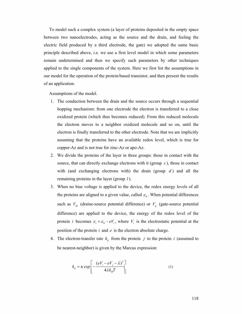
118
To model such a complex system (a layer of proteins deposited in the empty space
between two nanoelectrodes, acting as the source and the drain, and feeling the
electric field produced by a third electrode, the gate) we adopted the same basic
principle described above, i.e. we use a first level model in which some parameters
remain undetermined and then we specify such parameters by other techniques
applied to the single components of the system. Here we first list the assumptions in
our model for the operation of the protein/based transistor, and then present the results
of an application.
Assumptions of the model.
1. The conduction between the drain and the source occurs through a sequential
hopping mechanism: from one electrode the electron is transferred to a close
oxidized protein (which thus becomes reduced). From this reduced molecule
the electron moves to a neighbor oxidized molecule and so on, until the
electron is finally transferred to the other electrode. Note that we are implicitly
assuming that the proteins have an available redox level, which is true for
copper-Az and is not true for zinc-Az or apo-Az.
2. We divide the proteins of the layer in three groups: those in contact with the
source, that can directly exchange electrons with it (group s ), those in contact
with (and exchanging electrons with) the drain (group d ) and all the
remaining proteins in the layer (group l ).
3. When no bias voltage is applied to the device, the redox energy levels of all
the proteins are aligned to a given value, called 0ε . When potential differences
such as dsV (draine-source potential difference) or gV (gate-source potential
difference) are applied to the device, the energy of the redox level of the
protein i becomes 0i ieVε ε= − , where iV is the electrostatic potential at the
position of the protein i and e is the electron absolute charge.
4. The electron-transfer rate ijk from the protein j to the protein i (assumed to
be nearest-neighbor) is given by the Marcus expression:
2( )
4i j
ijB
eV eVk exp
k Tλ
κλ
− −= −
(1)
119
where λ is the reorganization energy of the ET process, Bk is the Boltzmann
constant and T is the absolute temperature (in the numerical calculation,
T = 300 K). The maximum rate constant κ was chosen to give the same rate
constant as two azurin self-exchanging an electron in solution (max. estimate:
≈106 s-1). As for the reorganization energy λ , we calculated it by using the
model described in the previous section applied to the transistor geometry (i.e.,
two proteins adsorbed on an insulating substrate), obtaining λ = 0.63 eV (the
dielectric constants used for SiO2 were optε =2.13 and 0ε =3.9).
5. The master equation for the evolution of the probability ip that the protein i
belonging to the group l is in the reduced form (also called occupation
number) is assumed to be:
(1 ) (1 )iij j i ji i j
j i j i
dp k p p k p pdt ≠ ≠
= − − −∑ ∑ (2)
(1 )ij j ik p p− is the rate of the ET from j to i ( ijk ) weighed by the probability
that the donor protein j is reduced ( jp ) and the acceptor protein i is oxidized
(1 ip− ). Similarly, (1 )ji i jk p p− is the rate of the ET from i to j ( jik )
weighed by the probability that the donor protein i is reduced ( ip ) and the
acceptor protein j is oxidized (1 jp− )
6. We assume that the ET between the source or the drain and the proteins in
group s or d , respectively, is much faster than the ET between two proteins.
This means that the occupation number of proteins si or di in groups s or d
is always that proper for equilibrium with the electrodes, i.e. Nernst law holds:
0
0
[ ( ) ]1 [ ( ) ]s
FS i Bi
FS i B
exp eV k Tpexp eV k T
ε εε ε
− − − /=
+ − − − / (3.1)
0
0
[ ( ( ) ]1 [ ( ( )) ]d
FS ds i Bi
FS ds i B
exp e V V k Tpexp e V V k T
ε εε ε
− − + − /=
+ − − + − / (3.2)
where dsV is the drain-source potential difference and FSε is the Fermi energy
of the source (we remark that all the potentials in the device are referred to the
source, which is always grounded).
Within these assumptions, the expression for the current is given by:
120
s
s
i
i
dpI e
dt= ∑ (4)
where si runs over all the proteins in direct contact with the source (a similar
expression can be found for the drain). The sign of the current is chosen to be positive
for electrons going from the electrode to the proteins.
The set of eqs. (2) has been solved numerically, by implementing a tailored
FORTRAN90 code. In addition to the protein-protein ET rate parameters κ and λ
whose choice we discussed above, the other parameters that have to be specified are:
(a) the positions of the proteins in the device; (b) the electrostatic potential at the
position of each protein as a function of dsV and gV ; and (c) the relative redox-level
energy of the proteins 0ε with respect to FSε (i.e., the difference 0 FSε ε− that appears
in eq.(3)).
(a) As for the protein positions, we considered a square lattice with lattice vectors
parallel and perpendicular to the source-drain direction. This assumption allows us to
study easily the dependence of the current on the size of the layer. The position could
be found as well with a simulation of adsorption of the proteins on the layer from a
solution. However, this would imply to average the current results for a given device
on a large number of different layer obtained by different simulations, which are
numerically very expensive. The simple square lattice can give results appropriate for
the level of description we are aiming to with a much smaller computational demand.
(b) The distribution of the potential in the device was found from a FEM simulation,
whose details are given in the appendix A.
(c) We are thus left with just one parameter, i.e., the energy level difference 0 FSε ε− .
This value could in principle be calculated by the work functions W of the metal
composing the electrodes and the standard reduction potential 0E of azurin. Using 5.3
eV for AuW [12], 0.3 V vs NHE (Normal Hydrogen Electrode) for 0E , and 4.6 eV for
the work function of the NHE, we estimate a value of 0 0 4FSε ε− = . eV. However,
such a value should not be taken too seriously, since the system is much more
complex than the simple assumptions at the basis of these data would imply (such as
protein in bulk solution and not dried and supported on an electrode, ultra-vacuum
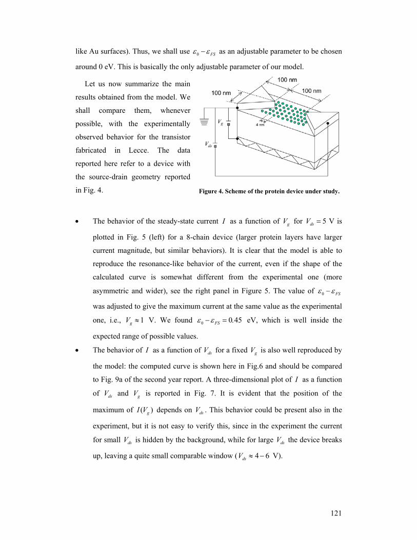
121
like Au surfaces). Thus, we shall use 0 FSε ε− as an adjustable parameter to be chosen
around 0 eV. This is basically the only adjustable parameter of our model.
Let us now summarize the main
results obtained from the model. We
shall compare them, whenever
possible, with the experimentally
observed behavior for the transistor
fabricated in Lecce. The data
reported here refer to a device with
the source-drain geometry reported
in Fig. 4.
• The behavior of the steady-state current I as a function of gV for dsV = 5 V is
plotted in Fig. 5 (left) for a 8-chain device (larger protein layers have larger
current magnitude, but similar behaviors). It is clear that the model is able to
reproduce the resonance-like behavior of the current, even if the shape of the
calculated curve is somewhat different from the experimental one (more
asymmetric and wider), see the right panel in Figure 5. The value of 0 FSε ε−
was adjusted to give the maximum current at the same value as the experimental
one, i.e., 1gV ≈ V. We found 0 0 45FSε ε− = . eV, which is well inside the
expected range of possible values.
• The behavior of I as a function of dsV for a fixed gV is also well reproduced by
the model: the computed curve is shown here in Fig.6 and should be compared
to Fig. 9a of the second year report. A three-dimensional plot of I as a function
of dsV and gV is reported in Fig. 7. It is evident that the position of the
maximum of ( )gI V depends on dsV . This behavior could be present also in the
experiment, but it is not easy to verify this, since in the experiment the current
for small dsV is hidden by the background, while for large dsV the device breaks
up, leaving a quite small comparable window ( 4 6dsV ≈ − V).
Figure 4. Scheme of the protein device under study.
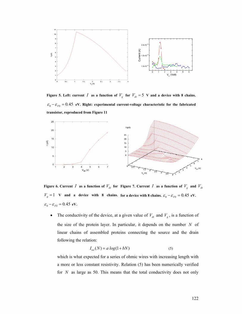
122
• The conductivity of the device, at a given value of dsV and gV , is a function of
the size of the protein layer. In particular, it depends on the number N of
linear chains of assembled proteins connecting the source and the drain
following the relation:
( ) (1 )totI N a log bN= + (5)
which is what expected for a series of ohmic wires with increasing length with
a more or less constant resistivity. Relation (5) has been numerically verified
for N as large as 50. This means that the total conductivity does not only
Figure 5. Left: current I as a function of gV for 5dsV = V and a device with 8 chains.
0 0 45FSε ε− = . eV. Right: experimental current-voltage characteristic for the fabricated
transistor, reproduced from Figure 11 of the second-year report.
Figure 6. Current I as a function of dsV for
1gV = V and a device with 8 chains.
0 0 45FSε ε− = . eV.
Figure 7. Current I as a function of gV and dsV
for a device with 8 chains. 0 0 45FSε ε− = . eV.
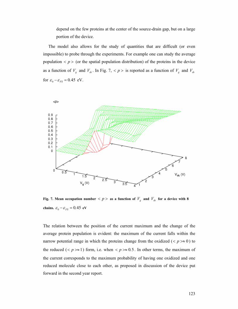
123
depend on the few proteins at the center of the source-drain gap, but on a large
portion of the device.
The model also allows for the study of quantities that are difficult (or even
impossible) to probe through the experiments. For example one can study the average
population p< > (or the spatial population distribution) of the proteins in the device
as a function of gV and dsV . In Fig. 7, p< > is reported as a function of gV and dsV
for 0 0 45FSε ε− = . eV.
Fig. 7. Mean occupation number p< > as a function of gV and dsV for a device with 8
chains. 0 0 45FSε ε− = . eV
The relation between the position of the current maximum and the change of the
average protein population is evident: the maximum of the current falls within the
narrow potential range in which the proteins change from the oxidized ( 0p< >≈ ) to
the reduced ( 1p< >≈ ) form, i.e. when 0 5p< >≈ . . In other terms, the maximum of
the current corresponds to the maximum probability of having one oxidized and one
reduced molecule close to each other, as proposed in discussion of the device put
forward in the second year report.
124
In conclusion, we elaborated a model based on a sequential conduction
mechanism, which is able to reproduce the main features of the experimentally
determined conductivity and trans-conductivity. Following this model, the resonance-
like behavior of the current correspond to the maximum probability of having two
nearest-neighbor proteins in different oxidation states. So far, the model gives a
satisfactory qualitative agreement of the resonance behavior of the IV curves in the
FET, but fails in the quantitative evaluation of the current. A more refined method,
which refines the protein-lead contacts and takes into account the presence of several
layers parallel to the substrate, is under evaluation and will be tested in the future.
References.
1. A. M. Kuznetsov, P. Sommer-Larsen, and J. Ulstrup, Surf. Sci. 275, 52 (1992). 2. E. P. Friis, Y. I. Kharkats, A. M. Kutznetsov, and J. Ulstrup, J. Phys. Chem. A
102, 7851 (1998). 3. W. Schmickler, Surf. Sci. 295, 43 (1993). 4. J. Tomasi, R. Cammi, B. Mennucci, C. Cappelli, and S. Corni, Phys. Chem.
Chem. Phys. 4, 5697 (2002). 5. A.A. Kornyshev, in The Chemical Physics of Solvation; R. Dogonadze, E.
Kámál, A.A. Kornyshev, J. Ulstrup, Eds.; Elsevier,: Amsterdam, 1985, Part A, p. 85, eq. 3.13.
6. (a) A. J. Di Bilio, M. G. Hill, N. Bonander, B. G. Karlsson, R. M. Villahermosa, B. G. Malmström, J. R. Winkler, and H.B. Gray, J. Am. Chem. Soc. 119, 9921 (1997); (b) H. B. Gray, B. G. Malmström, and R. J. P. Williams, J. Biol. Inorg. Chem. 5, 551 (2000).
7. U. Ryde, and M. H. M. Olsson, Int. J. Quant. Chem. 81, 335 (2001). 8. O. Teschke, G. Ceotto, and E. F. de Souza, Phys. Chem. Chem. Phys. 3, 2761
(2001). 9. A. Alessandrini, M. Gerunda, G. W. Canters, M. Ph. Verbeet, and P. Facci,
Chem. Phys. Lett. 376, 625 (2003). 10. I.M.C. van Amsterdam, M. Ubbink, O. Einsle, A. Messerschmidt, A. Merli, D.
Cavazzini, G.L. Rossi, and G.W. Canters, Nature Struct. Bio. 9, 48 (2002). 11. (a) A. Ferretti, A. Ruini, E. Molinari, and M. J. Caldas, Phys. Rev. Lett. 90,
086401 (2003); (b) A. Ferretti, A. Ruini, G. Bussi, E. Molinari, and M. Caldas, Phys. Rev. B in press, (2004).
12. H. B. Michaelson, J. Appl. Phys. 48, 4729 (1977).