this project presents a home brewed solution to ultra-high
TRANSCRIPT

This project presents a home brewed solution to high resolution Microscopy
Supervisors: Dr. Mashhood Ahmad
Dr. Sabieh Anwar (LUMS)
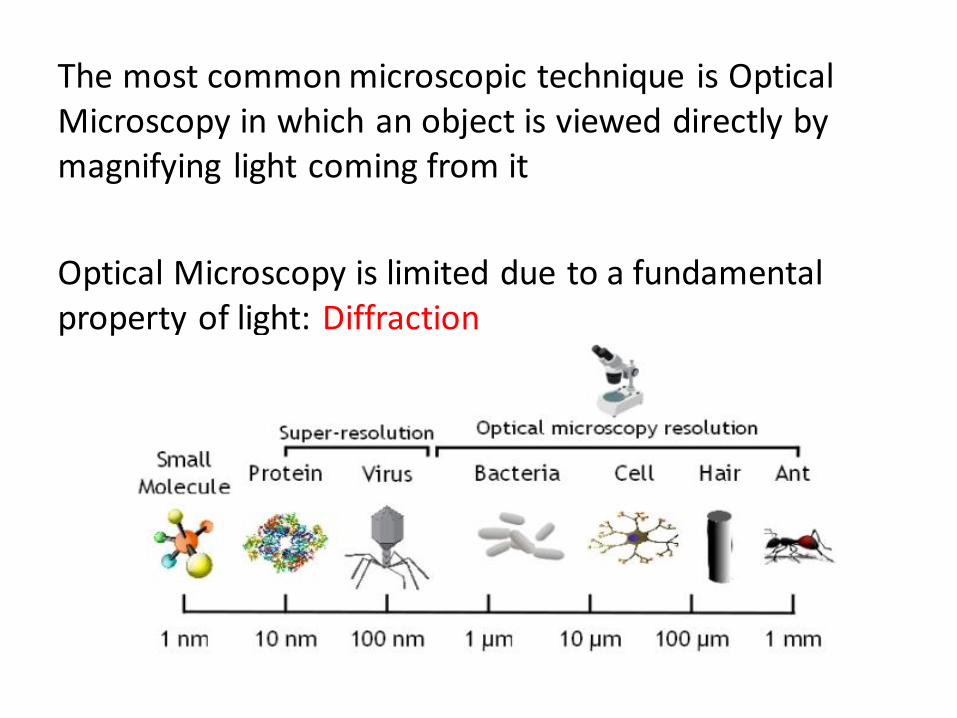
The most common microscopic technique is Optical Microscopy in which an object is viewed directly by magnifying light coming from it
Optical Microscopy is limited due to a fundamental property of light: Diffraction

Optical Limit
• Optical Microscopes can not resolve objects of size smaller than λ/2 (~ 250 nm for white light)

A new Microscopic Technique that goes beyond optical limit (introduced in late 80’s)
Atomic Force Microscopy (AFM) is a technique in which a sample is imaged indirectly using the atomic forces between its atoms and a very small probe
The atomic force between two atoms is a function of distance given by Lennard-Jones function
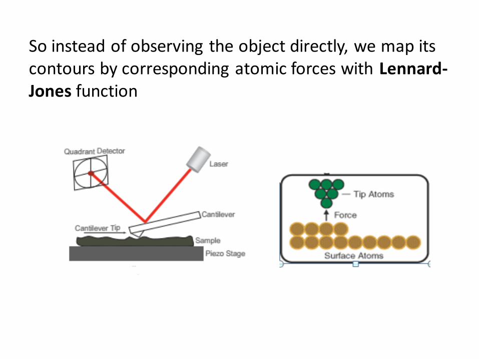
So instead of observing the object directly, we map its contours by corresponding atomic forces with Lennard-Jones function

Requirements for AFM
Measurements of small changes in laser reflection angle
Controlled Nano-scale motion in all axes to move probe pixel by pixel
Electronics and data acquisition system capable of detecting and amplifying variations in millivolts

ΔΦ
2ΔΦ
Diode Laser635nm
Collimating lens
Focusing lens
Position-Sensing Photodetector
Sample
Sample Mount
Laser Reflection Angle Detection Optical Setup

Laser Reflection Angle Detection AFM Probe
Silicon Nitride Probe
• Tip size: 32nm
• Top area 50x50 um approx.

Laser Reflection Angle Detection Position sensing Photodetector

Position sensing Photodetector
Response of Photodetector to 34.8mW laser beam. Signal shows Shot Noise of the detector
𝑆𝑁𝑅 =μ2
σ2= 2530.8

Controlled Nano-scale MotionX-Y Axis
Piezoelectric Discs (PZT) produce motion in nanometer precision when acted upon by large voltages
Required voltages go as high as 80V
Raster scan
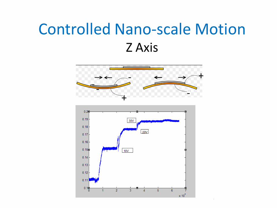
Controlled Nano-scale MotionZ Axis
+
+-
-

Electronics
• Bipolar high voltage power supply (100V)
• XYZ Piezo disc Drivers
• Signal Conditioning and feedback electronics
• Data Acquisition and processing with LabVIEW

Electronics100V (±50V) Bipolar supply
• Additional voltage regulator circuit to cancel ripples

ElectronicsX-Y axis Piezo Amplifier
Amplifier Stage
OPA445: High Voltage Op Amp
Maximum Output swing: 90V
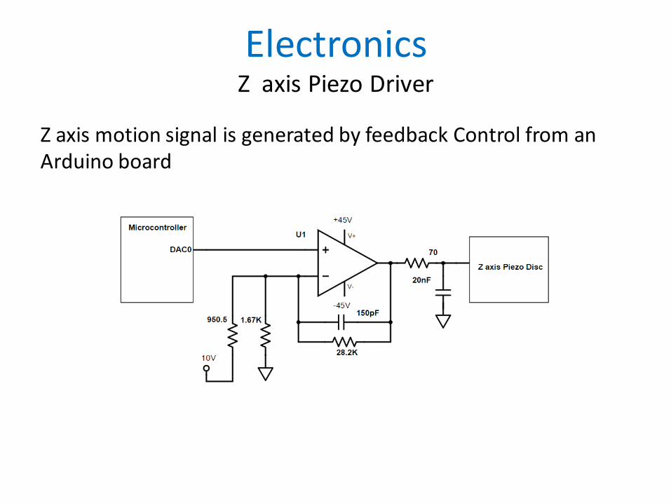
ElectronicsZ axis Piezo Driver
Z axis motion signal is generated by feedback Control from an Arduino board
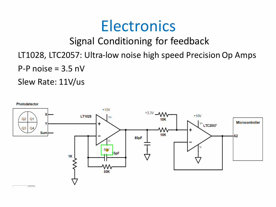
ElectronicsSignal Conditioning for feedback
LT1028, LTC2057: Ultra-low noise high speed Precision Op Amps
P-P noise = 3.5 nV
Slew Rate: 11V/us

ElectronicsData Flow
CPUNI DAQ Board
Photodetector
Arduino
PiezoActuator
Image Data
Z Driver Signal
X-Y Amplifier
Z Amplifier
X-Y Driver Signal
Feedback
Signal Conditioning
Feedback

User Interface

Feedback Control of AFM
Essential for scanning large samples (>500nm)

Feedback Control of AFM• Controller designed by Zeigler Nichols Method
• Noisy control loop: Kd=0
• PI controller will suit the AFM feedback
• Noise present at resonance frequencies of Piezoelectric actuator
• Control loop running at 1kHz sampling rate to avoid noise at resonance (50, 120 KHz)

AFM ImagingRaw Data from AFM
Smoothening filter
Generating Image
Image Processing
Final AFM Image
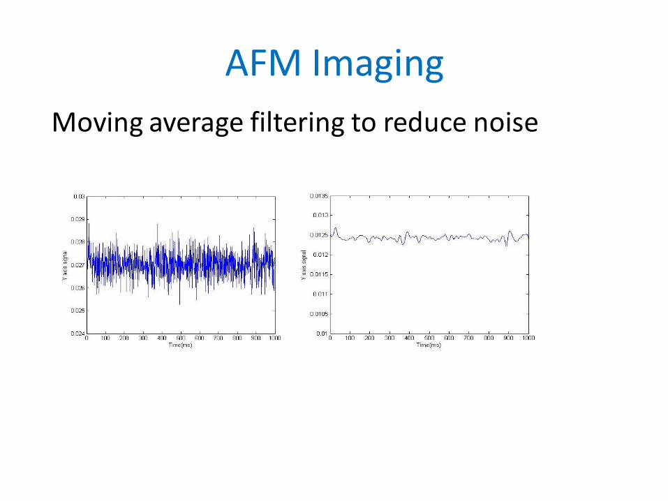
AFM Imaging
Moving average filtering to reduce noise

AFM ImagingGenerating Images

AFM ImagingGenerating Images
500nm

AFM Imaging
Generating Images
500nm

AFM ImagingRaw Data
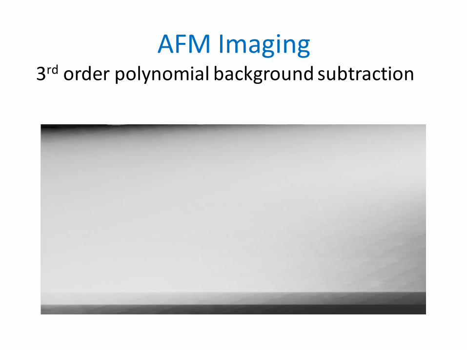
AFM Imaging3rd order polynomial background subtraction

AFM ImagingHistogram Specification

AFM Imaging
Cropping useful portion, high pass filtering

AFM ImagingAssigning color and scale
It is a 30nm grid!

Achievements
• Microscope is able to scan samples at “Super Resolution”
• Detection sensitivity for small objects is beyond any Optical or Electron Microscope with a fraction of the cost Approx. cost: PKR 200,000

Achievements
• Scan area = 12um x 10um
• Approx. Scan time = 16 minutes
• Height Resolution: up to 30nm
• Horizontal Resolution: 1.25nm Approx.
• Magnification: 600,000x (Calculated for grid sample)