thomas r. kurfess and thom j. hodgsonwtec.org/micromfg/report/05-metrology.pdf · this chapter...
TRANSCRIPT

65
CHAPTER 5
METROLOGY, SENSORS AND CONTROL
Thomas R. Kurfess and Thom J. Hodgson
ABSTRACT
This chapter focuses on metrology, sensors and controls for micromanufacturing. In general, a variety of sensors are employed in micromanufacturing. Many of them are used for metrology, and in particular dimensional metrology. Most are used on production machines to provide feedback during production. Few metrology systems for process and product control are available. The sensors and metrology systems available for product and process analysis are, in general, slow and not readily implemented. From a metrology and sensing perspective, the currently available systems are mostly two-dimensional in nature. Most of the measurement systems are fairly slow, which makes them suitable for R&D as their measurement speed limits their utility on actual production lines. Controllers fall into two architecture categories, open and closed (standard computer numerical control (CNC) controller architecture). In most cases, commercially available systems employ more traditional closed architecture controllers, while research and development teams tend to use open architecture systems. For most manufacturing systems, process control is a desired capability. In many cases it is achieved by measuring parameters from both the process and the product and adjusting process parameters to improve the quality of the part. In general, this approach is far from being achieved in the micromanufacturing field as the actual measurement of part and process parameters in real-time is limited to a few very special instances. Furthermore once a measurement is made, the process must be tuned according to the process model. In most cases, such models do not exist. Thus, in order to effectively achieve process control and quality enhancement, improved real-time metrology systems and sensors are needed along with models that accurately describe the various manufacturing processes at the micro level such that true process control can be enabled.
INTRODUCTION
Metrology, sensors and controls are critical for addressing quality control of micromanufactured products and processes. Quality control (QC) is one of the barriers to the growth of micromanufacturing both as an enabling technology and as a new market. Quality control not only provides quality assurance (QA)/QC but also feedback to optimize the design, fabrication, and assembly processes involved in the next generation of microsystems. QC may be divided into two equally important phases: R&D and production. From an R&D perspective, metrology is necessary for an understanding of the performance of newly developed products and processes. When a new design is generated and a prototype of that design is produced, the question that must be answered is, “Does this new design meet specifications?” The specifications will be both of a dimensional and performance nature. For example, if a gear train is designed, micrometrology systems will address not only the dimensional compliance of the individual gears, but also the assembly of the gears into the gear train. Other compliance issues that must be addressed for the gear train might include material parameters, dynamic performance and overall assembly compliance. From a production viewpoint, metrology is necessary to ensure that the products are fabricated correctly. Ultimately, the assurance of

5. Metrology, Sensors and Control 66
producing products that are “in specification” requires that the production process be controlled. Thus, metrology at the production level is used to understand and enhance production processes to ultimately yield microcomponents and systems that meet specifications. This understanding can be used to continuously improve production processes, resulting in continuous process and product improvement. In the end, the knowledge and understanding gained from metrology systems can be used to develop next-generation product and process designs.
This chapter discusses metrology systems as they apply to the dimensional measurement of microcomponents. Sensors are then discussed as they apply to both metrology and production systems. For the purposes of this report, the relationship between the two is assumed to be that metrology systems make use of a variety of individual sensors (for example, a scanning white light interferometer uses a microscope with a charged-couple device (CCD) camera and linear glass scales – making it a metrology system). Lastly, the chapter presents a review of controls used in micromanufacturing.
Metrology
In general, metrology is usually thought of as dimensional metrology that is used to verify component geometric dimensions. From this perspective, very little capability is available for microcomponent inspection. Most inspection that is currently done is accomplished using optical microscopes, scanning electron microscopes (SEM) and tunneling electron microscopes (TEM). Metrology with microscopes is executed in a fairly primitive manner using images from the microscope in conjunction with calibrated markings. Figure 5.1 is an example of such an image. The figure shows wear at the tip of a carbide cutting insert that is on the order of 100 µm in size (wear or tip size). The “100 µm” scale at the bottom is a typical scale marking. This particular picture was generated using an optical microscope. Inspection and metrology using these means is the equivalent of conducting dimensional measurement of mesoscale parts with a ruler or other scale indicator, and is not an accurate means of part geometry validation. For smaller components, electron microscope systems are also employed. However, these systems are even more difficult to use as they must be specially calibrated to make use of scale markings. For both optical and electron microscopes, the scale markings are generally intended to provide a “feel” for the size of the image, rather than a precise tool for metrology.
Microscopes used with calibrated optics and servo stages are being used fairly effectively for micrometrology. For this application, images are taken with well-calibrated microscopes; vision processing algorithms are then used to detect part edges and to analyze part geometry in 2D. These systems are limited to the resolution of the camera’s charge-coupled device (CCD) array, which is interfaced with the microscope. In general, these systems are 2D in nature, although the third dimension (height) can be resolved over the entire part using an autofocusing technique. These systems provide a trade-off between resolution and field of view. If higher resolution is desired, then a more powerful microscope objective is used. This limits the overall field of view. The microscope can be augmented with a servo stage that allows several images to be stitched, or aligned, together; however, stitching multiple images reduces the overall accuracy of the measurement. Such systems provide reasonable feedback for research and development purposes. However at present, they are too slow to be used in-line for production and process control purposes.
Some metrology is being done with atomic force microscope (AFM) systems, but mostly of this work is in the early stages of development and is targeted at nano-type applications. As implied by its name, AFMs have the capability to resolve geometries at the atomic level. However, such resolution is too fine for most microcomponent applications, making them somewhat useful as a research and development tool, but not as a production tool. AFMs are usually used as very high-resolution profilometers, making their measurements 2D in nature.
White light interferometry (WLI) and confocal microscopes appear to be leading metrology systems for 3D metrology in a number of research and development groups. There are a variety of WLI manufacturers that have commercially available products, although there are fewer producers of confocal microscopes. In general, U.S. manufacturers are the leading producers of WLI systems. Zeiss in Germany is the leading producer of confocal microscopes for micrometrology purposes. Both of these systems are based on the use of CCD cameras interfaced with a microscope to conduct measurements. Thus, the lateral resolution of these

Thomas R. Kurfess and Thom J. Hodgson 67
systems is limited by the pixel density on the CCD array. Furthermore, increased lateral resolution is realized by increasing the microscope objective power. Thus, just as with standard vision-based systems, there is a trade-off between field of view and lateral resolution. Servo stages can be used in conjunction with these systems to increase the lateral field of view; however, stitching issues reduce the effective accuracy of the overall measurement just as with microscope-based systems. Unlike microscope systems, WLI and confocal are most accurate in the vertical direction (out of plane). For example, a WLI is nominally presented as having sub-nanometer resolution. This is out-of-plane resolution, and is realized by the interferometric measurement that is made on the system. The in-plane (lateral) resolution is still limited by the WLI’s camera CCD pixel density and stage-positioning resolution (stitching). The other limitation of these two types of systems is that they must be used to measure relatively flat surfaces. Surfaces having angles of greater than approximately 10° do not reflect enough light to be measured.
Figure 5.1. Image from an optical microscope.
Presently, WLI and confocal systems are too slow for use in large-scale production. This is true if they are used as separate, stand-alone systems. Various research groups are looking to incorporate them directly into production machines for use in production machines. The difficulty with this approach is that such metrology systems can be very expensive. However, if micromanufacturing techniques can be used to fabricate a variety of the components necessary for these systems (e.g., lenses), then economies of scale may be affected, resulting in lower unit costs that may allow them to be more easily integrated into production systems. In particular, several institutions in Korea are building their own confocal microscopes and WLI systems in conjunction with Korean manufacturers, providing the latter with two types of experience that are critical for successful micromanufacturing. First, they are learning how to produce metrology systems. Second, they are learning how to integrate such systems into their production units. If these systems prove to be useful in production operations, Korean manufacturers will have an excellent foundation from which to launch a variety of commercial products.
There are several truly 3D systems that have been developed. One, presented by Professor Masuzawa at the University of Tokyo, is used primarily for R&D. It consists of a tactile probe that serves primarily as a sensor. This system is discussed in detail in a subsequent section of this chapter. Other, more developed systems include 3D coordinate measurement machines at Zeiss and at Japan’s National Institutes of Advanced Industrial Science and Technology (AIST). The Zeiss and AIST systems are shown in Figure 5.2 and Figure 5.3, respectively. Of these two systems, the Zeiss machine, known as the F25, has recently become commercially available. The F25 has several measuring sensors integrated with it as shown in Figure 5.4, including an optical sensor that performs the same function as the microscope-based inspection systems, a tactile measurement head that is used as a coordinate measuring machine (CMM) probe in both a point-to-point mode as well as a scanning mode, and a visualizing camera that is used to aid in the positioning of the tactile probe. The F25 is approximately 1.5 x 1.5 x 2 m3, has a measurement volume of 100 x 100 x 100 mm3, a three-dimensional scanning speed of 0.5 mm/s, a maximum single-axis speed of 20 mm/s, a

5. Metrology, Sensors and Control 68
maximum multi-axis speed of 35 mm/s and a maximum acceleration of 500 mm/s2. The volumetric accuracy of the F25 in point-to-point mode is 250 nm. The volumetric accuracy of the F25 in scanning mode has not been determined yet. The repeatability is 50 nm and it has a resolution of 7.8 nm. The machine is completely enclosed in it own environmental container. The projected cost for the F25 is approximately $500,000. The development of this system was partially supported by the government of Germany, and is based on collaborative research with the university partners of Zeiss.
Figure 5.2. Zeiss F25.
Figure 5.3. AIST CMM.
Tactile Scanning Probe
Optical Sensor
VisualizingCamera
Figure 5.4. Zeiss F25 sensor heads.
One of the most difficult aspects of implementing the micro CMM is the probe that interfaces between the microcomponent and the CMM. Figures 5.5 and Figure 5.6 show the probes of the F25 and the AIST machines, respectively. These probes are highly sensitive and consequently very fragile. The F25’s probe is placed on a silicone wafer substrate as shown in Figure 5.7. The wafer is etched to generate a flexure. This flexure is coated with a piezoresistive material that allows the probe deflection to be measured. Using this probe, the F25 is then servoed in a scanning mode in much the same fashion as other larger-scale scanning machines that Zeiss makes. Metrology software developed for other Zeiss CMMs is employed to analyze data from the F25. The smallest probe available for the F25 has a 120 µm diameter tip, with a maximum measurement depth (due to probe length) of 4 mm. Thus, the F25 is capable of measuring holes as small as

Thomas R. Kurfess and Thom J. Hodgson 69
150 µm with depths of up to 4 mm. It is the only such system that can make a true 3D measurement of such holes.
Figure 5.5. Zeiss F25 µCMM probe.
Figure 5.6. µCMM probe (AIST).
Membrane
Probe Shaft
Probe Sphere
Piezo-resistive Element
Silicon Wafer
Boss
Membrane
Probe Shaft
Probe Sphere
Piezo-resistive Element
Silicon Wafer
Boss
Figure 5.7. F25 µCMM probe design.
In conclusion, a variety of metrology systems are available for microcomponent inspection. However, few of them are 3D in nature. Furthermore, all of them are relatively slow and expensive, making them reasonable choices for R&D, but less-than-desirable choices for use in production lines. Even as faster and less-expensive systems become available, micrometrology systems will continue to face two major hurdles: edges and standards. All components have edges, and they are used to define the geometry of a part. Edge radii of 10-100 µm are typical for manufactured components. However, such sizes may be a significant fraction of a microcomponent’s dimensions or those of its features. Thus, the ability to characterize and edge accurately is critical, and has not been addressed to date. Finally, many of the standards that are applicable to macroscale metrology are not available for microscale metrology. Tools such as interferometers, ball bars and even gage blocks and gage balls, are not available at the micro-level for testing and calibrating micrometrology systems. As a result, the ability to calibrate and determine the capability of microscale metrology systems is limited.
Sensors
In general, sensors fall into one of two categories:
• Machine sensors—sensors that are used as feedback mechanisms for manufacturing and metrology systems
• Component sensors—sensors that are used to directly measure microscale components
The distinction between these two categories of sensors is important and must be made clear. Sensors that are used on manufacturing systems are readily available and are not necessarily “micro” in nature. For example, machine sensors measuring linear position may be 50–100 mm in length or even larger. However, they typically have a resolution of 1 nm or less. Furthermore, most of these sensors are used to measure in a single direction (example: along the X-axis), or at best need to have a single direction with an ultra-high resolution. This single high-resolution direction works well for most systems. Sensors used to measure
5. Metrology, Sensors and Control 70
microcomponents are those that actually take data from a component. These sensors typically must have minimal physical impact on the part. In fact, non-contacting sensors are desired. Furthermore, to acquire 3D metrology data, these sensors need to have ultra-high 3D resolution. Data from these sensors are used to verify part geometry and target dimensions. Machine sensors and component sensors are discussed separately in this section, due to the significant differences in their objectives and tasks.
Machine Sensors
The sensor of choice for providing feedback on production and manufacturing systems is the ultraprecision encoder. Nominally, the encoder comes in two variations, both of which are employed on micromanufacturing systems. The first is the linear scale used for measuring linear displacement. The second is a rotary encoder, used for measuring rotational motion. There are a variety of companies that make such encoders. In the case of the rotary encoder, which is an older and more developed technology, no particular supplier appears to dominate the market. However, Heidenhain (Germany) appears to be the dominant supplier of linear encoders, also known as linear glass scales. Most of the groups that were involved with micromanufacturing or micrometrology systems employed scales produced by Heidenhain when such feedback devices were used. Sony was also used or mentioned by a fair number of groups in Asia. FANUC indicated that they would use whatever type of linear scales a customer specifies on their ROBOnano, although they indicated the majority of systems were produced with Heidenhain scales, with Sony as the next most popular choice.
Both rotary and linear optical encoders have the advantage that they can be non-contact in nature, if care is taken in their incorporation into the machine metrology system. As shown in both Figure 5.8 and Figure 5.9, the read head does not contact the optical encoder. Thus, if the read head is mounted on an independent frame, also known as a metrology frame, it can be mechanically, thermally and electrically isolated from the scale. In many instances the use of a separate metrology frame enables designers to produce machines with superior accuracy and resolution.
Figure 5.8. Rotary encoder.
Figure 5.9. Linear encoder.
The other machine sensor that is heavily employed in the microfactory is the interferometer. Two types of interferometer are typically used in micromanufacturing applications. The first is the white light interferometer. This device is typically used to characterize the surface of a component, and is discussed in the ensuing section on component sensors. The second type of interferometer is the heterodyne laser interferometer. Similar to a linear encoder, this device measures relative motion of a device with ultra-high precision. The laser interferometer uses interference of laser light (typically HeNe at a wavelength, λ=632.8 nm, although less-stable solid-state lasers are sometimes employed). The laser interferometer can be used as a positional feedback mechanism in the same fashion as the linear encoder. It is also a non-contacting sensor that can be used quite effectively with a separate metrology frame to greatly enhance the overall machine accuracy. However, the laser interferometer is an expensive piece of equipment ($100,000 for a basic set-up), and is much more difficult to employ than a linear scale. Thus, the linear glass scale is preferred over the laser interferometer in all but the most demanding applications. Both the interferometer and the scales (linear and rotary) output a quadrature signal. This allows similar interface hardware to be employed when using both types of devices.
While laser interferometers are significantly more difficult to employ than glass scales, they can be used in conjunction with a machine’s scales to remove the machine’s repeatable scale errors via calibration. This procedure is known as error mapping. As the name suggests, the interferometer is used to map scale errors for each linear axis on the machine. The scale error is the difference between the position of the readout scale

Thomas R. Kurfess and Thom J. Hodgson 71
and that of a known reference (the laser interferometer) along the axis of motion. The procedure is relatively straightforward, the machine is moved a specific distance (e.g., 1 mm increments) and the error for each step is recorded. These errors are entered into the machine controller, which has the capability of compensating for the error. Typically, only scale errors are mapped on machining systems and metrology systems, although errors such as angular, straightness and squareness (29 total for a three axis (X, Y, Z) machine) can also be mapped. For example, the accuracy of the FANUC ROBOnano is 2.5 µm before error mapping, and is reduced to 10 nm with positional error mapping. Calibration is done at the factory, and the machine can be recalibrated on-site by an experienced professional. As most controllers are capable of error mapping scale errors, the only additional cost for this significant improvement in accuracy is the calibration. The machine requires no extra hardware. Error mapping is a major tool in achieving the target volumetric accuracy of a micromanufacturing system in a cost-effective manner.
Two primary difficulties must be addressed when using machine sensors with high resolution and relatively high-feed velocities: (1) the speed at which position increments must be counted, and (2) the number of position increments that must be counted. These issues are tightly related to the controls area and are discussed in more detail in that section of the chapter.
Sensors for Measuring Components
A vast number of new sensors have been used to measure components. A variety of other sensors have been specifically developed to measure components. In general, most sensor metrology applications target dimensional/geometric metrology (e.g., size, geometry, surface finish). However, there are a few sensors that are also targeting the ability to measure other quantities such as temperature, reflectivity, and a variety of material properties (e.g., Young’s modulus and the coefficient of thermal expansion). With one exception, all of the sensors that were seen during this visit were used for dimensional metrology. This section may be considered a bit redundant with respect to the metrology systems presented in the previous section. However, a bit more detail is presented in this section from a sensor perspective.
Many of the sensors for measuring the components have been discussed in the background report. In general, the sensing systems for geometric metrology can be divided into two sets of categories. The first category set is units that employ vision systems, cameras or devices that use pixel-type arrays, and those that do not. Vision-based systems include, but are not limited to white light interferometers, scanning electron microscopes and optical microscopes. X-ray tomography may also be grouped into this category, as X-ray sensors are comprised of pixel-based elements. Such devices rely on taking a “picture” of the device and, subsequently, performing some type of analysis (usually edge detection) on the data to determine quantities like size. Nominally, the resolution of such systems is limited by a combination of the magnification and the pixel density in the CCD array on the camera used to capture the data. In many instances, high resolution is achieved by using high magnification (e.g., using a higher powered optic in a microscope). In such cases, the range of the sensor is typically reduced. Thus, several data sets must be taken and stitched together. In this instance, it is the registering of each data set to the others that is typically the limiting factor of the system’s resolution. Thus, the increase in resolution generated by magnifying a part is typically offset by the resulting reduction of range (field of view).
To better illustrate this issue, Figure 5.10 shows a microgear that was inspected using a Zygo WLI. The major diameter of the gear is approximately 0.7 mm; with feature (tooth) sizes on the order of 100 µm. The direction of maximum sensitivity for the WLI is the Z direction, which is in and out of the plane of the image shown on the left part of Figure 5.10. The dimensions of interest in this particular inspection are the gear dimensions that are in the plane of this image. The high resolution direction of the WLI does show that the gear’s top surface is curved. This can easily be seen in the 3D image shown in Figure 5.10. This information is important, as it demonstrates that the lapping process employed to finish this particular part rounded the edges of the part. However, the part dimensions of interest such as major and minor diameter do not make use of the WLI’s interferometric resolution of less than 1 nm. Rather, the quantification of these dimensions is based on the lower lateral resolution of the WLI. Furthermore, the sidewalls of the part cannot be measured using the WLI, so no information for them is available at all. Thus, the resulting inspection can be considered 2.5D at best.

5. Metrology, Sensors and Control 72
Contact Non-Contact
2D
3D
Figure 5.10. Microgear Figure 5.11. Contact and non-contact
Sensors systems not employing vision type systems include contact probe systems such as AIST’s micro CMM (Figure 5.10).
The second category of sensor systems can be further divided into sensors that are nominally designed for 2D inspection, and those that are truly 3D in nature. In some instances, 2D systems can be used to measure 2.5D, but are not fully capable of measuring in 3D. An example of this is the WLI, which is primarily intended to measure surface finish characteristics, but has been used to generate 2D measurements. In the case of the WLI, the part’s edge is detected and it is this edge that is used for metrology. As previously discussed, edge detection is another issue limiting metrology systems’ capabilities that is discussed in the metrology section. Inspection of a part’s top surface is not a problem, but the fundamental principals that govern the operation of the WLI do not permit it to inspect the side walls of a part. In general, all 2D systems used for inspection are fundamentally limited to 2D inspection and cannot be employed for 3D inspection. The matrix shown in Figure 5.11 presents the breakdown of the two category sets for sensors and sensor systems used for dimensional metrology.
A variety of contacting cantilever-sensing devices has been developed for use in metrology. Four such microcantilever devices were demonstrated at Seiko Instruments, Inc. (SII) by Professor Matsuzawa: (1) the self-sensitive cantilever for displacement, (2) the nanoprobe for electrical resistivity, (3) the self-sensitive dual cantilever for multi-resolution displacement, and (4) the thermal cantilever for temperature measurements. The self-sensitive cantilever, which has been commercialized and used in dynamic force microscope (DFM) and AFM applications, is an alternative to the standard probes used on these systems. Standard probes employ an optical displacement measurement arrangement and require a laser and associated optics. The self-sensitive cantilever replaces the optical deflection measurement with strain measurements at the base of the cantilever by a piezoresistive element connected in a Wheatstone bridge configuration along with a reference resistance (Figure 5.12). The principal advantages are reduced overall size, the ability to be operated in the dark field, and ease of use and setup. Calibration is performed by using standard samples. The size of the cantilever is approximately W50 x L120 x T5 µm, with frequency response 300 kHz. The Nano4probe, fabricated by focused ion beam (FIB) technology, uses the four-point resistivity measurement method implemented by four narrowly pitched (200 nm) electrodes. The dual cantilever displacement probe uses a bimorph to switch between the large and small area scanning probes. The large area probe is used when ultra high-resolution measurements are not necessary. Thus, the dual cantilever displacement probe addresses the issues of the AFM having too great of a resolution for the inspection of most microcomponents. However, the high-resolution (small area) probe can be employed when the full resolution of the AFM is required.
The thermal cantilever for temperature measurements is one of the few sensors that were observed that were not developed for dimensional metrology; rather, this sensor is used to measure the temperature of microcomponents. Due to calibration issues, it would be difficult to use a thermocouple to measure the temperature of the part directly. This sensor employs a thermopile (a large number of thermocouples) to detect temperature differences between the probe (which is heated) and the surface of the inspected part. The thermopile provides feedback to the sensor as to the temperature difference between a calibrated and

Thomas R. Kurfess and Thom J. Hodgson 73
controlled temperature on the sensor and the microcomponent. The thermopile indicates if the temperature difference and the direction of that difference (e.g., higher or lower); it does not provide a value for the actual temperature difference. The probe reference temperature is modulated until there is no difference between the reference temperature and the component temperature. Then a thermocouple that has been calibrated for use on the probe’s reference temperature generator is used to measure the probe’s reference temperature.
Figure 5.12. Structure of self-sensitive cantilever.
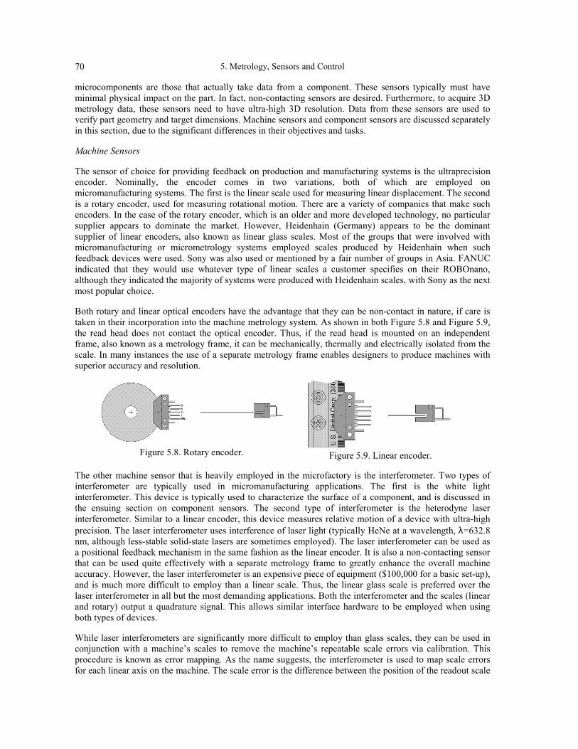
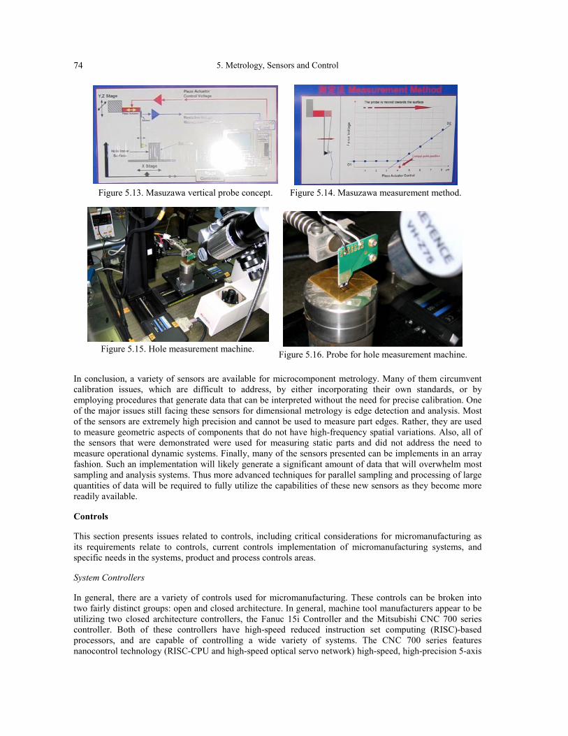
The metrology work done by Professor Masuzawa’s group at the University of Tokyo specifically targets the measurement of hole sidewalls. While this device is not a complete 3D measurement system, it does provide metrology information that is not available from most other measuring systems. Two major hurdles for most micrometrology systems are the measurement of side walls and the measurement of holes. As already discussed, measuring side walls is a difficult task as most optical-based systems do not receive enough light from a reflection of the side walls to make a meaningful measurement. Secondly, measuring a small hole requires that a probe be sent down the inside diameter of the hole, again a very challenging task (one that only the Zeiss F25 is currently capable of performing). Professor Masuzawa’s system addresses both of these two major issues. The system consists of a vertical probe as shown in Figure 5.13. The probe has a piezoresistive material on it that can be used to measure deflection. This is much the same as the probe shown to us at Zeiss and SII.
To make a measurement, the probe is servoed into the part as shown in Figure 5.14. The output of the probe is also shown in Figure 5.14. While the probe is not contacting the part, the horizontal line in the plot is generated (about 0–4 µm on the plot). Once the probe contacts that part, the voltage output of the probe increases linearly for small deflections as is shown in Figure 5.14 (4–8 µm). Figure 5.15 is a picture of the machine. Figure 5.16 is a close-up of the head. Basically, this approach generates two lines. These lines are fit and the intersection of these two lines is used as the contact or measurement point. This approach is much more robust, but slower than the SII technique. Robustness comes from the fact that the intersection of the two lines is used. If the sensitivity of the piezoresistive material changes, the slope of the second line will change; however, the intersection of the two lines will not. If there is noise, its effect is reduced by the fitting of the lines. This eliminates the need for the environmental add-on in the SII unit. The one disadvantage over the SII probe (Figure 5.12) is that the SII probe will be much faster, generating significantly more data per unit time than Masuzawa’s probe. From a CMM analogy, the Masuzawa approach is like a trigger CMM, going point-to-point. The SII probe is more of a scanning probe.
5. Metrology, Sensors and Control 74
Figure 5.13. Masuzawa vertical probe concept. Figure 5.14. Masuzawa measurement method.
Figure 5.15. Hole measurement machine.
Figure 5.16. Probe for hole measurement machine.
In conclusion, a variety of sensors are available for microcomponent metrology. Many of them circumvent calibration issues, which are difficult to address, by either incorporating their own standards, or by employing procedures that generate data that can be interpreted without the need for precise calibration. One of the major issues still facing these sensors for dimensional metrology is edge detection and analysis. Most of the sensors are extremely high precision and cannot be used to measure part edges. Rather, they are used to measure geometric aspects of components that do not have high-frequency spatial variations. Also, all of the sensors that were demonstrated were used for measuring static parts and did not address the need to measure operational dynamic systems. Finally, many of the sensors presented can be implements in an array fashion. Such an implementation will likely generate a significant amount of data that will overwhelm most sampling and analysis systems. Thus more advanced techniques for parallel sampling and processing of large quantities of data will be required to fully utilize the capabilities of these new sensors as they become more readily available.
Controls
This section presents issues related to controls, including critical considerations for micromanufacturing as its requirements relate to controls, current controls implementation of micromanufacturing systems, and specific needs in the systems, product and process controls areas.
System Controllers
In general, there are a variety of controls used for micromanufacturing. These controls can be broken into two fairly distinct groups: open and closed architecture. In general, machine tool manufacturers appear to be utilizing two closed architecture controllers, the Fanuc 15i Controller and the Mitsubishi CNC 700 series controller. Both of these controllers have high-speed reduced instruction set computing (RISC)-based processors, and are capable of controlling a wide variety of systems. The CNC 700 series features nanocontrol technology (RISC-CPU and high-speed optical servo network) high-speed, high-precision 5-axis

Thomas R. Kurfess and Thom J. Hodgson 75
control. These systems are closed architecture in nature, and the producers of these controls do not anticipate moving to a more open architecture.
The Bosch Rexroth IndraMotion MTX (Figure 5.19) is a new industrial controller that is entering the market and appears to be more open architecture in nature. Bosch intends to make use of these controllers for controlling their high-precision grinding and machining applications that produce a wide variety of microcomponents for their fuel injector and fuel pump divisions. The Siemens 840 series CNC controllers also have a somewhat open architecture capability. Both the Bosch and Siemens controllers will permit more advanced process control beyond the standard servo position control discussed above. For example, process control based on external inputs such as power, force or temperature may be executed with these controllers.
Figure 5.17. FANUC 15i controller.
Figure 5.18. Mitsubishi CNC 700 controller.
Most research and development groups visited employed open architecture systems produced by Delta Tau, D-Space, and National Instruments. The processing of data for these controllers is generally done with a combination of LabVIEW and MATLAB; although other programming languages are also employed. Few research groups employ any of the standard CNC controllers.
The FANUC series 15i control is used to control the ROBOnano ultra high-precision multi-function machine tool. It can function as a five-axis mill, a lathe, a five-axis grinder, a five-axis shaping machine and a high speed shaper. It uses friction free servo systems (all linear slides and screws are static air bearings). For milling, an air turbine spindle is employed for rotational speed up to 70,000 rpm. Shaping is done using a high-speed shuttle unit capable of producing three grooves per second, and a 3 kHz fast tool servo using a PZT actuator. Cutting is nominally accomplished with a single-crystal diamond tool. Error mapping on the 15i control is limited to positional (axial) errors only. The resolution of the linear axes is 1 nm and 0.00001° for the rotational axes. The design of the machine is such that it experiences no backlash and stick-slip motion. The size of the ROBOnano is 1270 x 1420 x 1500 mm. This does not include the CNC locker or the thermal management unit. However, in total, the machine is very compact. The range on the X-, Y- and Z-axes of the machine is 200 mm (horizontal, left and right) by 20 mm (horizontal, in and out) by 120 mm vertical, respectively. The maximum feed speed for the X- and Z-axes is 200 mm/min, and 20 mm/min for the Y-axis. The development of ROBOnano was partially supported by the government of Japan.

5. Metrology, Sensors and Control 76
Figure 5.19. Bosch Rexroth IndraMotion MTX.
Figure 5.20. FANUC ROBOnano machine
tool.
Issues Related to Control
Several major issues are specifically related to the control of micromachine tools. They include higher speed controllers, position counters having higher resolution capabilities, spline interpolation, higher order motion control and environmental control. Increased controller speed is critical for micromachine implementation for several reasons. First the higher speed allows for smoother interpolation. Second, servoing at ultra-high resolution (on the order of 1 nm) demands that the controller is capable of tracking encoders at very high rates. For example, if a machine has 1 nm resolution and is traveling at federate of just 1 mm/s, the controller must track an encoder pulse at a rate of 1 pulse/µs, resulting in a 1 MHz clock requirement. If the system is traveling at 1 m/s, an encoder pulse is generated every ns, requiring a 1 GHz clock. If this same machine has a one-meter range, the controller must be able to track a billion encoder counts, requiring a 30-bit (minimum) counter. The speed at which the encoders must be read in conjunction with the range of the encoder counts is significant and outside of most standard controller specifications. Thus, only very high-end controllers are used in such applications.
In order to generate smoother trajectories, spline interpolation is used in conjunction with high-resolution, high-speed controllers. The spline interpolation results in improved surface finish, especially over shorter-range motions. Furthermore, trajectory planning and control are accomplished on the machine’s position, velocity, acceleration, and jerk (the time derivative of the acceleration). This differs from typical machine control where only the position, velocity and acceleration are considered. The incorporation of jerk into both the trajectory planning and control results in smoother and more consistent machine motion trajectories. Error mapping is employed on almost all of the micromachine tools (and measurement systems). For all systems reviewed, only positional (axial) error maps were developed and used. Thus, angular and straightness errors were not considered. Positional error mapping appears to be sufficient to achieve the desired machine accuracies at the present time. As an example of the utility of positional error mapping, the accuracy of FANUC’s ROBOnano was increased by a factor of 100 via error mapping.
Finally, given the size of the micromachine tools and of CMMs, many of them are enclosed in their own environmental chambers. This enables tight control of the machine tool’s temperature, reducing variations due to thermal expansion and enhancing the machine’s accuracy. Typically the environmental control uses an air shower temperature control unit, whose temperature is controlled to 0.1°C. To demonstrate the importance of thermal control, the following example is presented. The thermal coefficient of expansion of steel is approximately 12 parts per million per degree C. Thus, a bar of steel 1 m in length grows 12 µm for every degree Celsius that it is heated. This is a significant amount of change when producing microcomponents. Coolant temperatures are also controlled to an even tighter level.

Thomas R. Kurfess and Thom J. Hodgson 77
Open Architecture Controls / Control Flexibility
There is a clear dichotomy regarding the utilization of open architecture controls in the micromanufacturing area. Most of the research and development is done on an open architecture and flexible platform. This is true at academic institutions, government laboratories and in industry. A variety of controllers were seen including PC-based controllers operating with real-time systems, single-board motion controllers (usually employing a PC as the interface for programming), and field programmable gate arrays (FPGA). However, from an industry/implementation perspective, closed architecture controllers using hardware based on application specific integrated circuit (ASIC) systems are employed.
Even with the “closed architecture” controls such as the FANUC or Mitsubishi controllers, a single controller can run multiple types of machines. For example, ROBOnano can be configured for milling, turning, shaping and several other operations using the same FANUC 15i controller. While these controllers are flexible, they are not open architecture. It appears that the mainstream control companies in Japan sucha s FANUC and Mistubishi will not move into the open architecture market. The German control companies such as Siemens and Bosch appear to provide a more open architecture platform; however, these controllers are still not as open as the DSP and FPGA controllers.
Process Control
The ultimate goal of controlling a micromachine tool is to control the machining process. While significant work is being conducted in the realm of servo control of machine tools, little is being done regarding process control. For example, positioning accuracy and repeatability were amply demonstrated. However, the effect of a cutting process, such as milling or turning, on the overall machine performance was not demonstrated. For a variety of ultra high-production processes, the actual cutting dynamics must be considered so that the process can be controlled well enough to achieve the desired results. Thus, the ability to control parameters other than tool position trajectory will be important in micromachining. Furthermore, process control implies that there is a process model available to use in actuator trajectory generation. For most micromachining processes, models do not exist. Furthermore, it has been shown for a variety of processes that micro-level process models are not accurately represented via macro-level models. Thus, new process models for the micro-level must be developed before process control can be properly executed.
In conclusion a variety of controllers that can adequately control micromachine tools are available. These controllers are flexible in nature and can be either open or closed architecture depending on the application. The systems are capable of controlling a variety of process parameters, resulting in some of the most accurate machine tools available on the market. However, to fully control various processes, improved and more accurate process models are required. These will have to be developed before true process control can be achieved.
SUMMARY AND CONCLUSIONS
In general, a variety of 2D and 2.5D metrology systems are currently available. They are relatively expensive and slow, but are useful for initial microcomponent and system R&D. From the standpoints of both robustness and inspection speed, metrology systems lack the ability to be used in a production setting from both a robustness perspective as well as an inspection speed perspective. There are a few truly 3D metrology systems. These systems are quite capable, but are expensive and, again, are not built for a mass-production environment. The sensors that are available for micromachines are adequate for single-axis position control. Other sensors are currently being developed, but are not yet well enough developed for industrial-scale use. In particular, a sensor is needed to interface metrology systems to the small-scale microcomponents. Ideally, this sensor would be non-contact, have high resolution and high bandwidth. This would enable high-speed, high-precision dynamic measurements of microcomponents and systems.
Controllers are evolving to address a number of issues raised in controlling micromanufacturing systems. In particular, they are operating at higher speeds, communicating with drives and sensors at higher speeds, generating smoother trajectories (position, velocity, acceleration and jerk) that result in smoother and more
5. Metrology, Sensors and Control 78
accurate surfaces. They have faster quadrature decoders with higher counting capabilities to allow them to properly track high resolution motions over the machine tool’s range. Controllers are also becoming more flexible to address the variety of processes that are being used in the microfactory. While they are becoming more reconfigurable—for example, controlling a lathe and a mill—major control system manufacturers in Asia are not looking towards open architecture controllers. These companies control the majority of the CNC market, and their customers are not requesting controllers that make use of open architectures. Thus, there is no great incentive to move in that direction. Those using open architecture controllers in Asia are typically using single-board open architecture controllers fabricated in the U.S. and Europe. While machine control has progressed quite well, process control has not. This is primarily due to a lack of models, process understanding, and experience. Thus, significant efforts are needed in developing micromanufacturing process models and the controllers and control algorithms to utilize these models to improve the overall process and, ultimately, the product.
REFERENCES
CNC Family SINUMERIK, http://www2.automation.siemens.com/mc/mc-sol/en/ 701ecff2-0611-47eb-8be8-73d4be9f33cd/index.aspx (Accessed October 20, 2005)
Rexroth IndraMotion MTX, http://www.boschrexroth.com/country_units/america/united_states/en/products/brc/a_downloads/ 71237AE0104_final.pdf (Accessed October 20, 2005)
Super 5-axis Nano Machine FANUC ROBOnano alpha-0iB, http://www.fanuc.co.jp/en/product/robonano/index.htm (Accessed October 5, 2005)