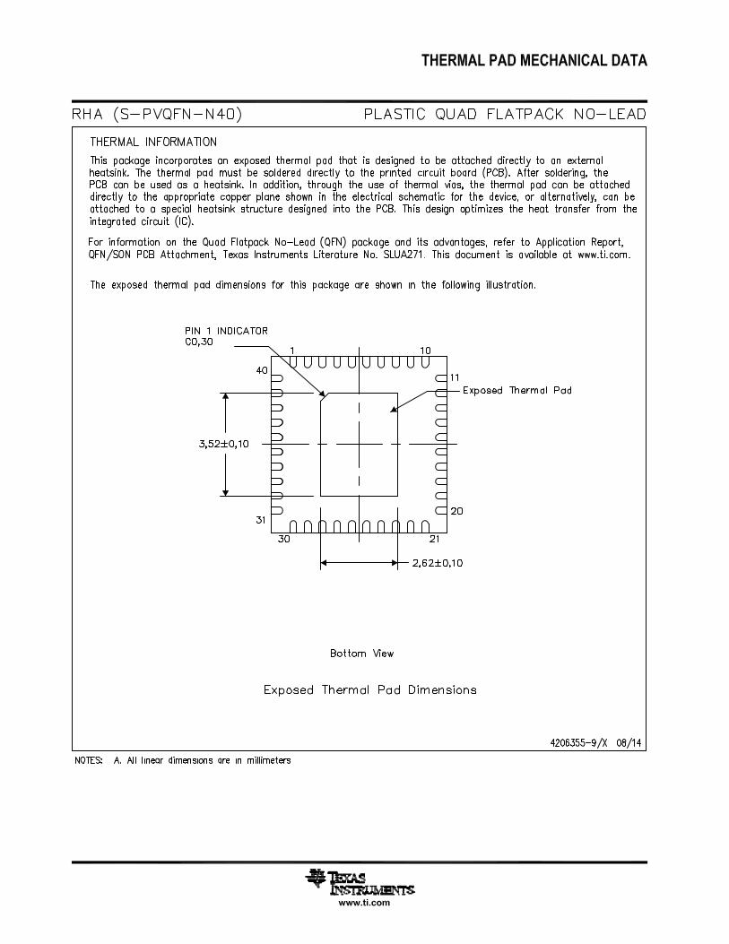
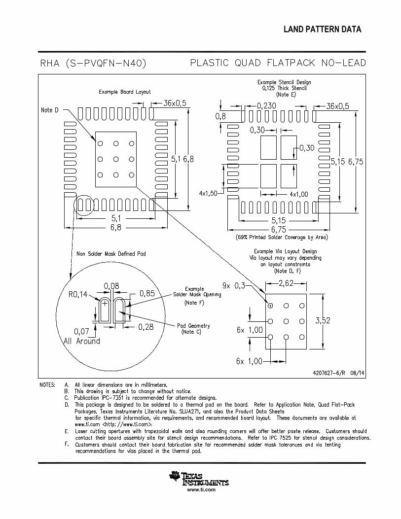
three dc-dc converters with integrated fet (rev. b) - ti.com · tps652510 slvsb30b –september...
TRANSCRIPT
TPS652510
www.ti.com SLVSB30B –SEPTEMBER 2011–REVISED AUGUST 2013
4.5-V TO 16-V INPUT, HIGH CURRENT, SYNCHRONOUS STEP DOWN THREE DC-DCCONVERTERS WITH INTEGRATED FET
Check for Samples: TPS652510
1FEATURES • Adjustable Cycle-by-Cycle Current Limit Setby External Resistor• Wide Input Supply Voltage Range:
• Current-Mode Control With Simple4.5 V - 16 VCompensation Circuit• 0.8-V, 1% Accuracy Reference
• Automatic Low Pulse Skipping (PSM) Power• Continuous Loading:Mode, Allowing for an Output Ripple Better3 A (Buck1), 2 A (Buck2 and 3)than 2%• Maximum Current:
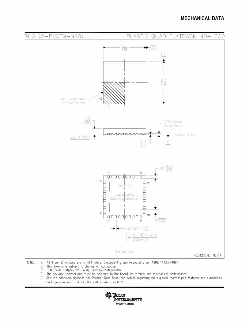
• Support Pre-Biased Outputs3.5 A (Buck 1), 2.5 A (Buck2 and 3)• Power Good Supervisor and Reset Generator• Synchronous Operation, 300-kHz – 2.2-MHz• Small, Thermally Efficient 40-Pin 6-mm x 6-mmSwitching Frequency Set By External Resistor
RHA (QFN) package• External Enable Pins With Built-In Current• -40°C to 125°C Junction Temperature RangeSource for Easy Sequencing
• External Soft Start Pins
DESCRIPTION/ORDERING INFORMATIONTPS652510 is a power management IC with three step-down buck converters. Both high-side and low-sideMOSFETs are integrated to provide fully synchronous conversion with higher efficiency. The converters aredesigned to simplify its application while giving the designer the option to optimize their usage according to thetarget application.
The converters can operate in 5-, 9-, 12- or 15-V systems. The output voltage can be set externally using aresistor divider to any value between 0.8 V and the input supply minus the resistive drops on the converter path.Each converter features enable pin that allows a delayed start-up for sequencing purposes, soft start pin thatallows adjustable soft-start time by choosing the soft-start capacitor, and a current limit (RLIM) pin that enablesdesigner to adjust current limit by selecting an external resistor and optimize the choice of inductor. All convertersoperate in ‘hiccup mode’: Once an over-current lasting more than 10 ms is sensed in any of the converters, theywill shut down for 10 ms and then the start-up sequencing will be tried again. If the overload has been removed,the converter will ramp up and operate normally. If this is not the case the converter will see another over-currentevent and shuts down again repeating the cycle (hiccup) until the failure is cleared. If an overload condition lastsfor less than 10 ms, only the relevant converter affected will shut-down and re-start and no global hiccup modewill occur.
The switching frequency of the converters is set by an external resistor connected to ROSC pin. The switchingregulators are designed to operate from 300 kHz to 2.2 MHz. The converters operate with 180° phase betweenthen to minimize the input filter requirements. All converters have peak current mode control which simplifiesexternal frequency compensation.
The device has a built-in slope compensation ramp to prevent sub harmonic oscillations in peak current modecontrol. A traditional type II compensation network can stabilize the system and achieve fast transient response.Moreover, an optional capacitor in parallel with the upper resistor of the feedback divider provides one more zeroand makes the crossover frequency over 100 kHz.
All converters feature an automatic low power pulse PFM skipping mode which improves efficiency during lightloads and standby operation, while guaranteeing a very low output ripple, allowing for a value of less than 2% atlow output voltages.
1
Please be aware that an important notice concerning availability, standard warranty, and use in critical applications ofTexas Instruments semiconductor products and disclaimers thereto appears at the end of this data sheet.
PRODUCTION DATA information is current as of publication date. Copyright © 2011–2013, Texas Instruments IncorporatedProducts conform to specifications per the terms of the TexasInstruments standard warranty. Production processing does notnecessarily include testing of all parameters.
TPS652510
SLVSB30B –SEPTEMBER 2011–REVISED AUGUST 2013 www.ti.com
The device incorporates an overvoltage transient protection circuit to minimize voltage overshoot. The OVPfeature minimizes the output overshoot by implementing a circuit to compare the FB pin voltage to OVP thresholdwhich is 109% of the internal voltage reference. If the FB pin voltage is greater than the OVTP threshold, thehigh side MOSFET is disabled preventing current from flowing to the output and minimizing output overshoot.When the FB voltage drops lower than the OVP lower threshold which is 107%, the high side MOSFET isallowed to turn on the next clock cycle.
TPS652510 features a supervisor circuit which monitors each buck’s output and the PGOOD pin is assertedonce sequencing is done. The PGOOD pin is an open drain output. The PGOOD pin is pulled low when anybuck converter is pulled below 85% of the nominal output voltage. The PGOOD is pulled up when all converteroutputs are more than 90% of its nominal output voltage. The default reset time is 100 ms. The polarity of thePGOOD is active high.
The device implements an internal thermal shutdown to protect itself if the junction temperature exceeds 160°C.The thermal shutdown forces the device to stop operating when the junction temperature exceeds thermal tripthreshold. Once the die temperature decreases below 140°C, the device reinitiates the power up sequence. Thethermal shutdown hysteresis is 20°C.
ORDERING INFORMATION (1)
TA PACKAGE (2) PART NUMBER TOP-SIDE MARKING-40°C to 125°C 40-Pin (QFN) - RHA Reel of 2500 TPS652510RHAR TPS652510
(1) For the most current packaging and ordering information, see the Package Option Addendum at the end of this document, or see the TIweb site at www.ti.com.
(2) Package drawings, thermal data, and symbolization are available at www.ti.com/packaging.
2 Submit Documentation Feedback Copyright © 2011–2013, Texas Instruments Incorporated
Product Folder Links: TPS652510
BUCK1
BUCK2
BUCK3
V3V
V7V
CLOCKROSC
VIN1
RLIM1
EN1
BST1
LX1
LX1
FB1
CMP1
BST2
LX2
LX2
FB2
CMP2
BST3
LX3
LX3
FB3
CMP3
12V
SS1
VIN2
RLIM2
EN2
SS2
VIN3
RLIM3
EN3
SS3
CV3P3
CV7
ROSC
CSS1
CSS2
CSS3
RILIM1
RILIM2
RILIM3
CBST1
CBST2
CBST3
LDC1
LDC2
LDC3
RCMP1 CCMP1
RCMP2 CCMP2
RFB1U
RFB1L
RFB2U
RFB2L
RFB3U
RFB3L
CODC2
CODC3
CODC1
CIDC1
CIDC2
CIDC3
for sequenced start-up
External enable
External enable
External enable
for sequenced start-up
for sequenced start-up
+
Low Power mode
Low Power mode
Low Power mode
CCMP22
CCMP11
Biasing
0.8V
0.8V
0.8V
1µA
1µA
1µA
PG&RST generator
PGOOD
VPULL
CCMP33
High for forced PWMLow por autoamtic PFM/PWM mode
F_PWM
RCMP3 CCMP3
TPS652510
www.ti.com SLVSB30B –SEPTEMBER 2011–REVISED AUGUST 2013
This integrated circuit can be damaged by ESD. Texas Instruments recommends that all integrated circuits be handled withappropriate precautions. Failure to observe proper handling and installation procedures can cause damage.
ESD damage can range from subtle performance degradation to complete device failure. Precision integrated circuits may be moresusceptible to damage because very small parametric changes could cause the device not to meet its published specifications.
FUNCTIONAL BLOCK DIAGRAM
Copyright © 2011–2013, Texas Instruments Incorporated Submit Documentation Feedback 3
Product Folder Links: TPS652510
TPS652510
QFN RHA40
RL
IM3
EN1
SS
1
CO
MP
1
FB
1
RO
SC
F_P
WM
FB
2
CO
MP
2
SS
2
EN2
LX1
LX1
VIN1
BST1
1 2 3 4 5 6
11
12
13
14
15
16
17
18
19
20
BST2
VIN2
7 8 9 10
RL
IM2
LX2
LX2
V7V
V3V
UC
PG
OO
D
RL
IM1
LX3
LX3
VIN3
BST3
29 28 27 26 25 24 23 22 2130
UC
40
39
38
37
36
35
34
33
32
31
EN3
SS
3
CO
MP
3
FB
3
UC
UC
UC
UC
UC
UC
TPS652510
UC
UC
LX3
UC
LX3
BST3
VIN3
EN3
FB
1
SS
1
CM
P1
RO
SC
RLIM
1
CM
P3
RLIM
3
FB
3
SS
3
LX2
BST2
LX1
VIN2
LX2
EN2
VIN1
EN1
LX1
BST1
CM
P2
FB
2
SS
2
V7V
PG
OO
D
V3
V
V1
VIN1
UC
V3
VIN3
VIN2
RLIM
2
V2
FB
3
FB
1
FB
2
EOR
VPULL
UC
UC
UC
UC
FB2
FB1
FB3
F_
PW
MH
ost
Optional
TPS652510
SLVSB30B –SEPTEMBER 2011–REVISED AUGUST 2013 www.ti.com
TYPICAL APPLICATION
PIN OUT
4 Submit Documentation Feedback Copyright © 2011–2013, Texas Instruments Incorporated
Product Folder Links: TPS652510
TPS652510
www.ti.com SLVSB30B –SEPTEMBER 2011–REVISED AUGUST 2013
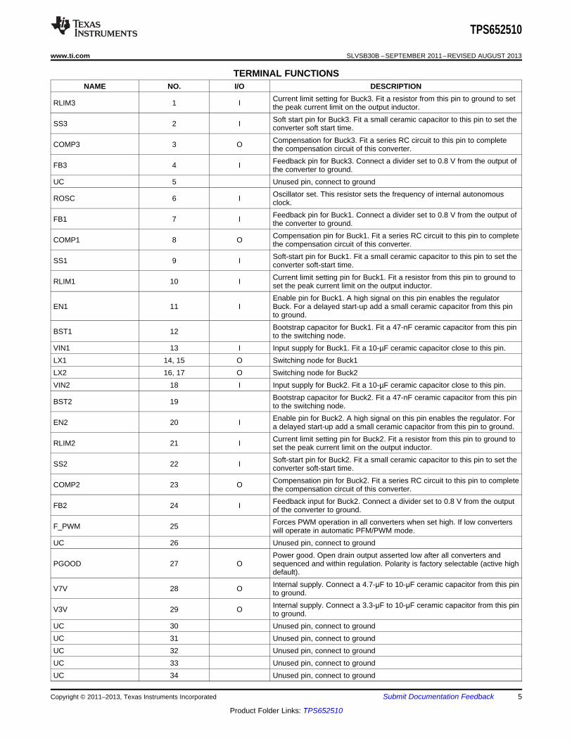
TERMINAL FUNCTIONSNAME NO. I/O DESCRIPTION
Current limit setting for Buck3. Fit a resistor from this pin to ground to setRLIM3 1 I the peak current limit on the output inductor.Soft start pin for Buck3. Fit a small ceramic capacitor to this pin to set theSS3 2 I converter soft start time.Compensation for Buck3. Fit a series RC circuit to this pin to completeCOMP3 3 O the compensation circuit of this converter.Feedback pin for Buck3. Connect a divider set to 0.8 V from the output ofFB3 4 I the converter to ground.
UC 5 Unused pin, connect to groundOscillator set. This resistor sets the frequency of internal autonomousROSC 6 I clock.Feedback pin for Buck1. Connect a divider set to 0.8 V from the output ofFB1 7 I the converter to ground.Compensation pin for Buck1. Fit a series RC circuit to this pin to completeCOMP1 8 O the compensation circuit of this converter.Soft-start pin for Buck1. Fit a small ceramic capacitor to this pin to set theSS1 9 I converter soft-start time.Current limit setting pin for Buck1. Fit a resistor from this pin to ground toRLIM1 10 I set the peak current limit on the output inductor.Enable pin for Buck1. A high signal on this pin enables the regulator
EN1 11 I Buck. For a delayed start-up add a small ceramic capacitor from this pinto ground.Bootstrap capacitor for Buck1. Fit a 47-nF ceramic capacitor from this pinBST1 12 to the switching node.
VIN1 13 I Input supply for Buck1. Fit a 10-µF ceramic capacitor close to this pin.LX1 14, 15 O Switching node for Buck1LX2 16, 17 O Switching node for Buck2VIN2 18 I Input supply for Buck2. Fit a 10-µF ceramic capacitor close to this pin.
Bootstrap capacitor for Buck2. Fit a 47-nF ceramic capacitor from this pinBST2 19 to the switching node.Enable pin for Buck2. A high signal on this pin enables the regulator. ForEN2 20 I a delayed start-up add a small ceramic capacitor from this pin to ground.Current limit setting pin for Buck2. Fit a resistor from this pin to ground toRLIM2 21 I set the peak current limit on the output inductor.Soft-start pin for Buck2. Fit a small ceramic capacitor to this pin to set theSS2 22 I converter soft-start time.Compensation pin for Buck2. Fit a series RC circuit to this pin to completeCOMP2 23 O the compensation circuit of this converter.Feedback input for Buck2. Connect a divider set to 0.8 V from the outputFB2 24 I of the converter to ground.Forces PWM operation in all converters when set high. If low convertersF_PWM 25 will operate in automatic PFM/PWM mode.
UC 26 Unused pin, connect to groundPower good. Open drain output asserted low after all converters and
PGOOD 27 O sequenced and within regulation. Polarity is factory selectable (active highdefault).Internal supply. Connect a 4.7-μF to 10-μF ceramic capacitor from this pinV7V 28 O to ground.Internal supply. Connect a 3.3-μF to 10-μF ceramic capacitor from this pinV3V 29 O to ground.
UC 30 Unused pin, connect to groundUC 31 Unused pin, connect to groundUC 32 Unused pin, connect to groundUC 33 Unused pin, connect to groundUC 34 Unused pin, connect to ground
Copyright © 2011–2013, Texas Instruments Incorporated Submit Documentation Feedback 5
Product Folder Links: TPS652510
TPS652510
SLVSB30B –SEPTEMBER 2011–REVISED AUGUST 2013 www.ti.com
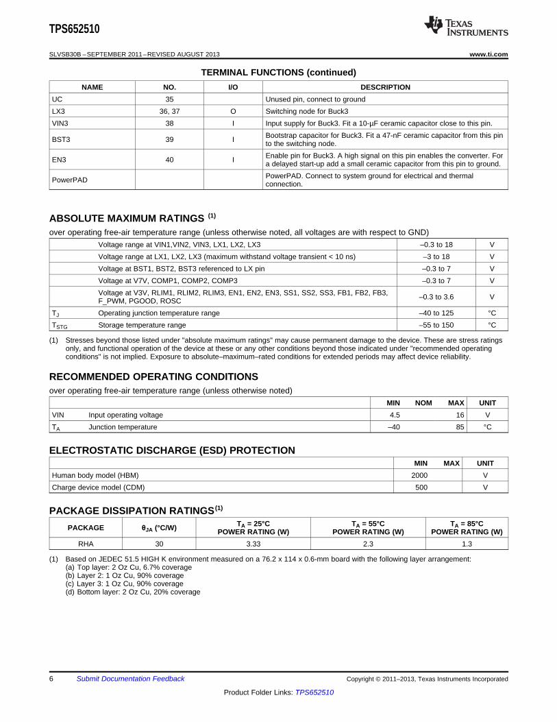
TERMINAL FUNCTIONS (continued)NAME NO. I/O DESCRIPTION
UC 35 Unused pin, connect to groundLX3 36, 37 O Switching node for Buck3VIN3 38 I Input supply for Buck3. Fit a 10-µF ceramic capacitor close to this pin.
Bootstrap capacitor for Buck3. Fit a 47-nF ceramic capacitor from this pinBST3 39 I to the switching node.Enable pin for Buck3. A high signal on this pin enables the converter. ForEN3 40 I a delayed start-up add a small ceramic capacitor from this pin to ground.PowerPAD. Connect to system ground for electrical and thermalPowerPAD connection.
ABSOLUTE MAXIMUM RATINGS (1)
over operating free-air temperature range (unless otherwise noted, all voltages are with respect to GND)Voltage range at VIN1,VIN2, VIN3, LX1, LX2, LX3 –0.3 to 18 VVoltage range at LX1, LX2, LX3 (maximum withstand voltage transient < 10 ns) –3 to 18 VVoltage at BST1, BST2, BST3 referenced to LX pin –0.3 to 7 VVoltage at V7V, COMP1, COMP2, COMP3 –0.3 to 7 VVoltage at V3V, RLIM1, RLIM2, RLIM3, EN1, EN2, EN3, SS1, SS2, SS3, FB1, FB2, FB3, –0.3 to 3.6 VF_PWM, PGOOD, ROSC
TJ Operating junction temperature range –40 to 125 °CTSTG Storage temperature range –55 to 150 °C
(1) Stresses beyond those listed under "absolute maximum ratings" may cause permanent damage to the device. These are stress ratingsonly, and functional operation of the device at these or any other conditions beyond those indicated under "recommended operatingconditions" is not implied. Exposure to absolute–maximum–rated conditions for extended periods may affect device reliability.
RECOMMENDED OPERATING CONDITIONSover operating free-air temperature range (unless otherwise noted)
MIN NOM MAX UNITVIN Input operating voltage 4.5 16 VTA Junction temperature –40 85 °C
ELECTROSTATIC DISCHARGE (ESD) PROTECTIONMIN MAX UNIT
Human body model (HBM) 2000 VCharge device model (CDM) 500 V
PACKAGE DISSIPATION RATINGS (1)
TA = 25°C TA = 55°C TA = 85°CPACKAGE θJA (°C/W) POWER RATING (W) POWER RATING (W) POWER RATING (W)RHA 30 3.33 2.3 1.3
(1) Based on JEDEC 51.5 HIGH K environment measured on a 76.2 x 114 x 0.6-mm board with the following layer arrangement:(a) Top layer: 2 Oz Cu, 6.7% coverage(b) Layer 2: 1 Oz Cu, 90% coverage(c) Layer 3: 1 Oz Cu, 90% coverage(d) Bottom layer: 2 Oz Cu, 20% coverage
6 Submit Documentation Feedback Copyright © 2011–2013, Texas Instruments Incorporated
Product Folder Links: TPS652510
TPS652510
www.ti.com SLVSB30B –SEPTEMBER 2011–REVISED AUGUST 2013
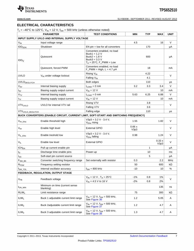
ELECTRICAL CHARACTERISTICSTJ = –40°C to 125°C, VIN = 12 V, fSW = 500 kHz (unless otherwise noted)
PARAMETER TEST CONDITIONS MIN TYP MAX UNITINPUT SUPPLY UVLO AND INTERNAL SUPPLY VOLTAGEVIN Input voltage range 4.5 16 VIDDSDN Shutdown EN pin = low for all converters 170 µA
Converters enabled, no loadBuck1 = 1.2 V
Quiescent Buck2 = 1.8 V 600 µABuck3 = 3.3 VIDDQ TA = 25°C, F_PWM = LowConverters enabled, no loadQuiescent, forced PWM 18 mAF_PWM = High, L = 4.7 µHRising VIN 4.22
UVLO VIN under voltage lockout VFalling VIN 4.1
UVLODEGLITCH Both edges 110 µsV3V Internal biasing supply ILOAD = 0 mA 3.2 3.3 3.4 VI3V Biasing supply output current VIN = 12 V 10 mAV7V Internal biasing supply ILOAD = 0 mA 5.63 6.25 6.88 VI7V Biasing supply output current VIN = 12 V 10 mA
Rising V7V 3.8V7VUVLO UVLO for internal V7V rail V
Falling V7V 3.6V7VUVLO_DEGLITCH Falling edge 110 µsBUCK CONVERTERS (ENABLE CIRCUIT, CURRENT LIMIT, SOFT-START AND SWITCHING FREQUENCY)
V3p3 = 3.2 V - 3.4 V,VIH_ENx Enable threshold high 1.55 1.82 VVENx rising0.66 xVIH Enable high level External GPIO VV3p3
V3p3 = 3.2 V - 3.4 V,VIL_ENx Enable treshold low 0.98 1.24 VVENx falling0.33 xVIL Enable low level External GPIO VV3p3
ICHEN Pull up current enable pin 1 µAtD Discharge time enable pins Power-up 10 msISS Soft-start pin current source 5 µAFSW_BK Converter switching frequency range Set externally with resistor 0.3 2.2 MHzRFSW Frequency setting resistor 50 600 kΩfSW_TOL Internal oscillator accuracy fSW = 800 kHz -10 10 %FEEDBACK, REGULATION, OUTPUT STAGE
VIN = 12 V , TA = 25°C -1% 0.8 1%VFB Feedback voltage V
VIN = 4.5 V to 16 V -2% 0.8 2%Minimum on time (current sensetON_MIN 135 nsblanking)
RLIMx Limit resistance range 75 300 kΩVIN = 12 V, fSW = 500 kHz,ILIM1 Buck 1 adjustable current limit range 1.2 5.05 ASee Figure 36VIN = 12 V, fSW = 500 kHz,ILIM2 Buck 2adjustable current limit range 1.2 4.7 ASee Figure 37VIN = 12 V, fSW = 500 kHz,ILIM3 Buck 3 adjustable current limit range 1.3 4.7 ASee Figure 38
Copyright © 2011–2013, Texas Instruments Incorporated Submit Documentation Feedback 7
Product Folder Links: TPS652510
TPS652510
SLVSB30B –SEPTEMBER 2011–REVISED AUGUST 2013 www.ti.com
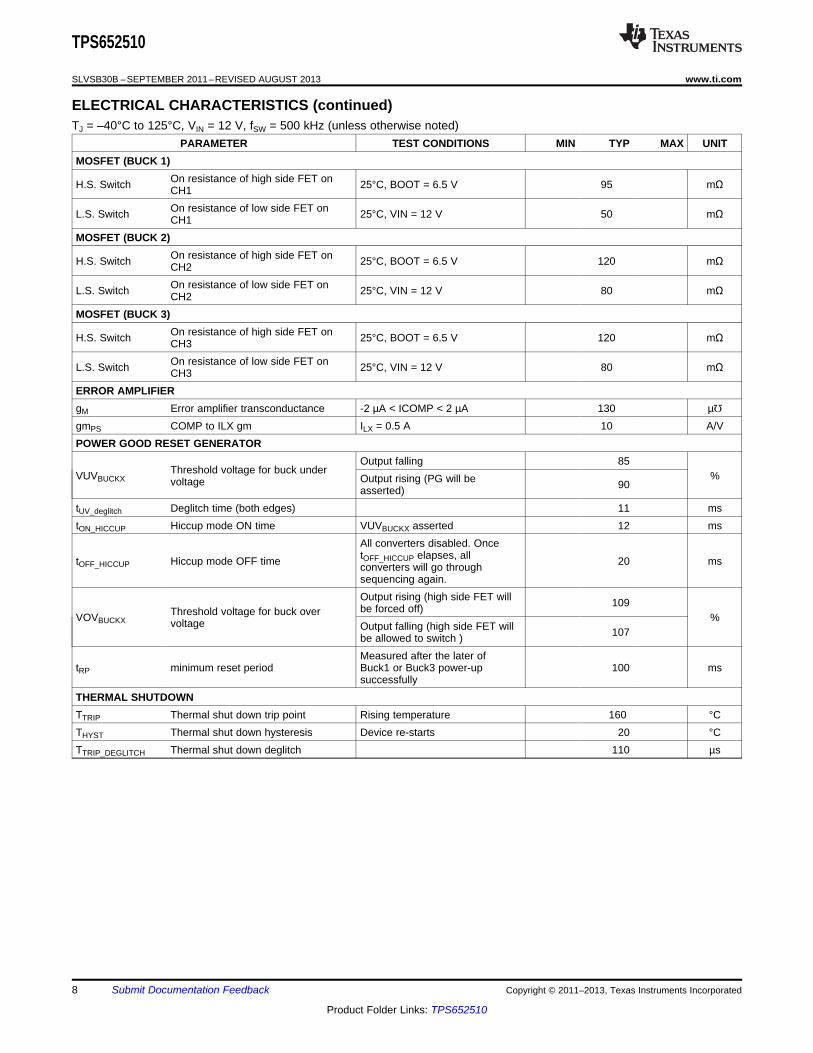
ELECTRICAL CHARACTERISTICS (continued)TJ = –40°C to 125°C, VIN = 12 V, fSW = 500 kHz (unless otherwise noted)
PARAMETER TEST CONDITIONS MIN TYP MAX UNITMOSFET (BUCK 1)
On resistance of high side FET onH.S. Switch 25°C, BOOT = 6.5 V 95 mΩCH1On resistance of low side FET onL.S. Switch 25°C, VIN = 12 V 50 mΩCH1
MOSFET (BUCK 2)On resistance of high side FET onH.S. Switch 25°C, BOOT = 6.5 V 120 mΩCH2On resistance of low side FET onL.S. Switch 25°C, VIN = 12 V 80 mΩCH2
MOSFET (BUCK 3)On resistance of high side FET onH.S. Switch 25°C, BOOT = 6.5 V 120 mΩCH3On resistance of low side FET onL.S. Switch 25°C, VIN = 12 V 80 mΩCH3
ERROR AMPLIFIERgM Error amplifier transconductance -2 µA < ICOMP < 2 µA 130 µgmPS COMP to ILX gm ILX = 0.5 A 10 A/VPOWER GOOD RESET GENERATOR
Output falling 85Threshold voltage for buck underVUVBUCKX %Output rising (PG will bevoltage 90asserted)
tUV_deglitch Deglitch time (both edges) 11 mstON_HICCUP Hiccup mode ON time VUVBUCKX asserted 12 ms
All converters disabled. OncetOFF_HICCUP elapses, alltOFF_HICCUP Hiccup mode OFF time 20 msconverters will go throughsequencing again.Output rising (high side FET will 109be forced off)Threshold voltage for buck overVOVBUCKX %voltage Output falling (high side FET will 107be allowed to switch )Measured after the later of
tRP minimum reset period Buck1 or Buck3 power-up 100 mssuccessfully
THERMAL SHUTDOWNTTRIP Thermal shut down trip point Rising temperature 160 °CTHYST Thermal shut down hysteresis Device re-starts 20 °CTTRIP_DEGLITCH Thermal shut down deglitch 110 µs
8 Submit Documentation Feedback Copyright © 2011–2013, Texas Instruments Incorporated
Product Folder Links: TPS652510
3
3.1
3.2
3.3
3.4
3.5
3.6
3.7
3.8
3.9
-40 -20 0 20 40 60
Temperature - °C
ILIM
1 -
PK
buck2 = 2 A,
buck3 = 2 A
buck2 = 0 A,
buck3 = 0 A
20
30
40
50
60
70
80
90
Eff
icie
ncy -
%
0 0.5 1 1.5 2 2.5 3
Current - A
V = 12 VI
V = 15 VI
V = 4.5 VI
1.21
1.215
1.22
1.225
1.23
V_B
UC
K1 -
V
-40 -20 0 20 40 60
Temperature - °C
0 0.2 0.4 0.6 0.8 1 1.2 1.4 1.6 1.8 2
I_BUCK3 - A
3.365
3.37
3.375
3.38
3.385
V_B
UC
K3 -
V
I_buck1 = 0.25 A,I_buck2 = 0.25 A
I_buck1 = 1 A,I_buck2 = 1 A
I_buck1 = 2 A,I_buck2 = 2 A
0 0.5 1 1.5 2 2.5 3
I_BUCK1 - A
1.2
1.205
1.21
1.215
1.22
1.225
V_B
UC
K1 -
V
I_buck2 = 2 A,I_buck3 = 2 A I_buck2 = 1 A,
I_buck3 = 1 A
I_buck2 = 0.25 A,I_buck3 = 0.25 A
1.8
1.805
1.81
1.815
1.82
1.825
V_B
UC
K2 -
V
0 0.2 0.4 0.6 0.8 1 1.2 1.4 1.6 1.8 2
I_BUCK2 - A
I_buck2 = 2 A,I_buck3 = 2 A I_buck1 = 1 A,
I_buck3 = 1 A
I_buck1 = 0.25 A,I_buck3 = 0.25 A
TPS652510
www.ti.com SLVSB30B –SEPTEMBER 2011–REVISED AUGUST 2013
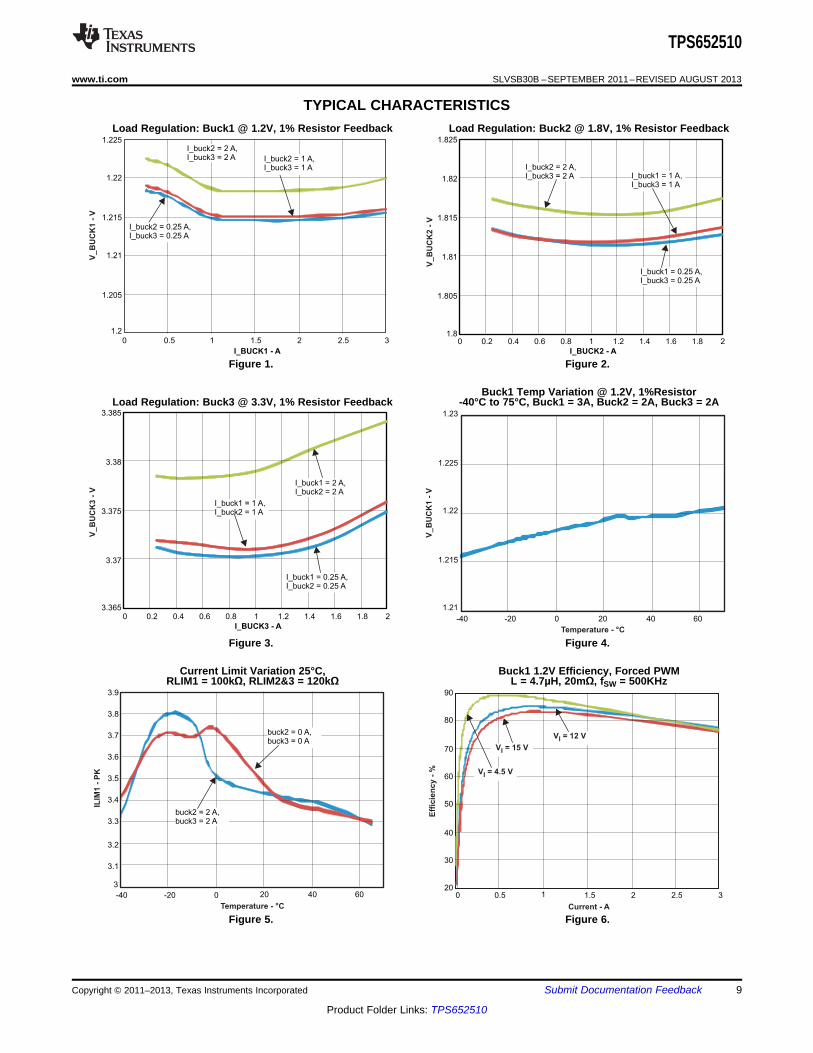
TYPICAL CHARACTERISTICSLoad Regulation: Buck1 @ 1.2V, 1% Resistor Feedback Load Regulation: Buck2 @ 1.8V, 1% Resistor Feedback
Figure 1. Figure 2.
Buck1 Temp Variation @ 1.2V, 1%ResistorLoad Regulation: Buck3 @ 3.3V, 1% Resistor Feedback -40°C to 75°C, Buck1 = 3A, Buck2 = 2A, Buck3 = 2A
Figure 3. Figure 4.
Current Limit Variation 25°C, Buck1 1.2V Efficiency, Forced PWMRLIM1 = 100kΩ, RLIM2&3 = 120kΩ L = 4.7µH, 20mΩ, fSW = 500KHz
Figure 5. Figure 6.
Copyright © 2011–2013, Texas Instruments Incorporated Submit Documentation Feedback 9
Product Folder Links: TPS652510
0 25 50 75 100 125 150 175 200 225 250 275 300 325 350 375 400
Current - mA
0
10
20
30
40
50
60
70
80
90
Eff
icie
ncy -
%
PWM
PFM
0
10
20
30
40
50
60
70
80
90
Eff
icie
ncy -
%
0 25 50 75 100 125 150 175 200 225 250 275 300 325 350 375 400
Current - mA
PWM
PFM
V = 12 VI
V = 15 VI
V = 4.5 VI
20
30
40
50
60
70
80
90E
ffic
ien
cy -
%
0 0.2 0.4 0.6 0.8 1 1.2 1.4 1.6 1.8 2
Current - A
0
10
20
30
40
50
60
70
80
90
Eff
icie
ncy -
%
0 25 50 75 100 125 150 175 200 225 250 275 300 325 350 375 400
Current - mA
PFM
PWM
20
30
40
50
60
70
80
90
Eff
icie
ncy -
%
0 0.2 0.4 0.6 0.8 1 1.2 1.4 1.6 1.8 2
Current - A
V = 12 VI
V = 15 VI
V = 4.5 VI
TPS652510
SLVSB30B –SEPTEMBER 2011–REVISED AUGUST 2013 www.ti.com
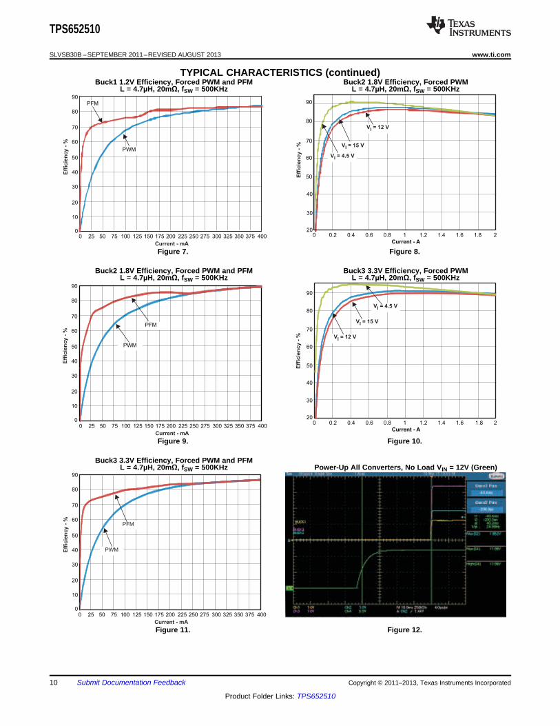
TYPICAL CHARACTERISTICS (continued)Buck1 1.2V Efficiency, Forced PWM and PFM Buck2 1.8V Efficiency, Forced PWM
L = 4.7µH, 20mΩ, fSW = 500KHz L = 4.7µH, 20mΩ, fSW = 500KHz
Figure 7. Figure 8.
Buck2 1.8V Efficiency, Forced PWM and PFM Buck3 3.3V Efficiency, Forced PWML = 4.7µH, 20mΩ, fSW = 500KHz L = 4.7µH, 20mΩ, fSW = 500KHz
Figure 9. Figure 10.
Buck3 3.3V Efficiency, Forced PWM and PFML = 4.7µH, 20mΩ, fSW = 500KHz Power-Up All Converters, No Load VIN = 12V (Green)
Figure 11. Figure 12.
10 Submit Documentation Feedback Copyright © 2011–2013, Texas Instruments Incorporated
Product Folder Links: TPS652510
TPS652510
www.ti.com SLVSB30B –SEPTEMBER 2011–REVISED AUGUST 2013
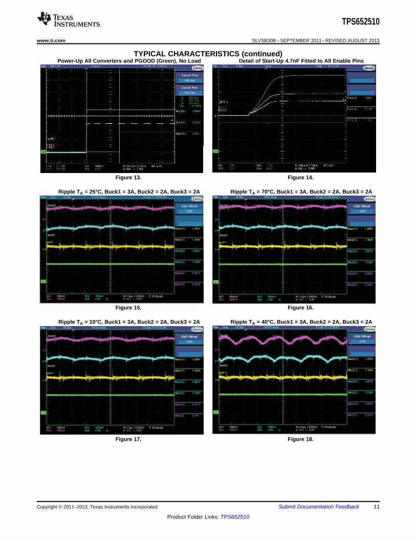
TYPICAL CHARACTERISTICS (continued)Power-Up All Converters and PGOOD (Green), No Load Detail of Start-Up 4.7nF Fitted to All Enable Pins
Figure 13. Figure 14.
Ripple TA = 25°C, Buck1 = 3A, Buck2 = 2A, Buck3 = 2A Ripple TA = 70°C, Buck1 = 3A, Buck2 = 2A, Buck3 = 2A
Figure 15. Figure 16.
Ripple TA = 10°C, Buck1 = 3A, Buck2 = 2A, Buck3 = 2A Ripple TA = 40°C, Buck1 = 3A, Buck2 = 2A, Buck3 = 2A
Figure 17. Figure 18.
Copyright © 2011–2013, Texas Instruments Incorporated Submit Documentation Feedback 11
Product Folder Links: TPS652510
TPS652510
SLVSB30B –SEPTEMBER 2011–REVISED AUGUST 2013 www.ti.com
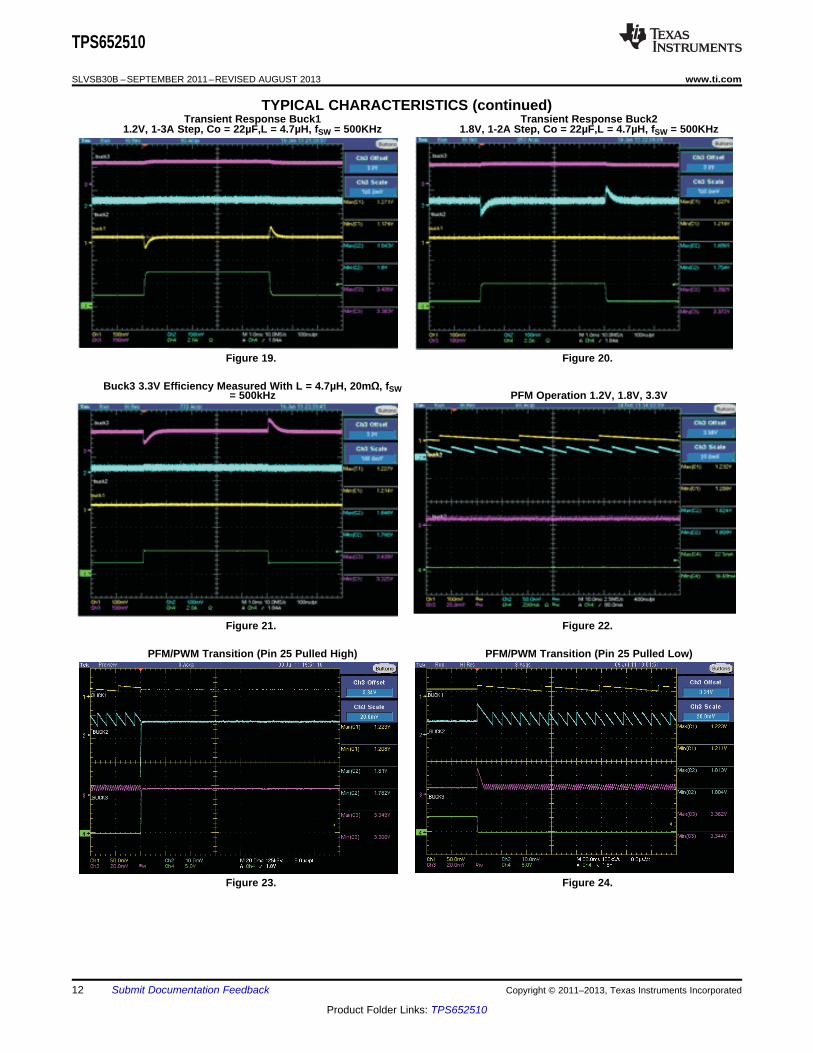
TYPICAL CHARACTERISTICS (continued)Transient Response Buck1 Transient Response Buck2
1.2V, 1-3A Step, Co = 22µF,L = 4.7µH, fSW = 500KHz 1.8V, 1-2A Step, Co = 22µF,L = 4.7µH, fSW = 500KHz
Figure 19. Figure 20.
Buck3 3.3V Efficiency Measured With L = 4.7µH, 20mΩ, fSW= 500kHz PFM Operation 1.2V, 1.8V, 3.3V
Figure 21. Figure 22.
PFM/PWM Transition (Pin 25 Pulled High) PFM/PWM Transition (Pin 25 Pulled Low)
Figure 23. Figure 24.
12 Submit Documentation Feedback Copyright © 2011–2013, Texas Instruments Incorporated
Product Folder Links: TPS652510
TPS652510
www.ti.com SLVSB30B –SEPTEMBER 2011–REVISED AUGUST 2013
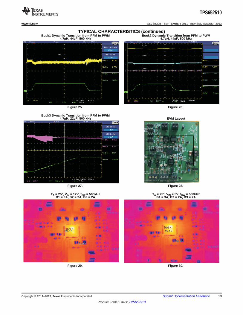
TYPICAL CHARACTERISTICS (continued)Buck1 Dynamic Transition from PFM to PWM Buck2 Dynamic Transition from PFM to PWM
4.7µH, 44µF, 500 kHz 4.7µH, 44µF, 500 kHz
Figure 25. Figure 26.
Buck3 Dynamic Transition from PFM to PWM4.7µH, 22µF, 500 kHz EVM Layout
Figure 27. Figure 28.
TA = 25°, VIN = 12V, fSW = 500kHz TA = 25°, VIN = 5V, fSW = 500kHzB1 = 3A, B2 = 2A, B3 = 2A B1 = 3A, B2 = 2A, B3 = 2A
Figure 29. Figure 30.
Copyright © 2011–2013, Texas Instruments Incorporated Submit Documentation Feedback 13
Product Folder Links: TPS652510
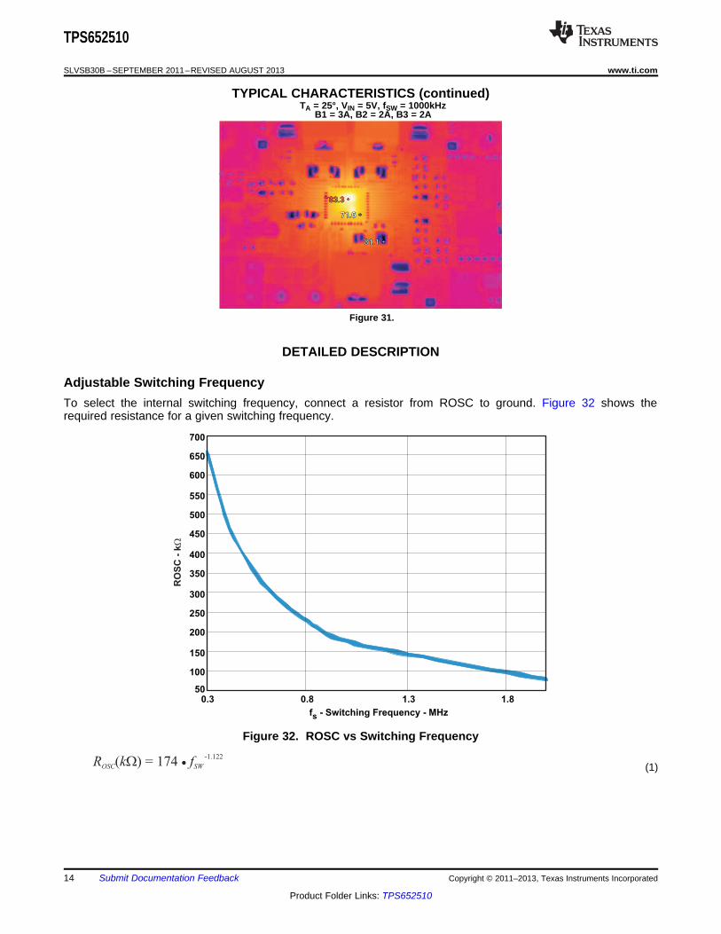
R k fOSC SW( ) = 174W ·-1.122
50
100
150
200
250
300
350
400
450
500
550
600
650
700
0.3 0.8 1.3 1.8
f - Switching Frequency - MHzs
RO
SC
- k
W
TPS652510
SLVSB30B –SEPTEMBER 2011–REVISED AUGUST 2013 www.ti.com
TYPICAL CHARACTERISTICS (continued)TA = 25°, VIN = 5V, fSW = 1000kHz
B1 = 3A, B2 = 2A, B3 = 2A
Figure 31.
DETAILED DESCRIPTION
Adjustable Switching FrequencyTo select the internal switching frequency, connect a resistor from ROSC to ground. Figure 32 shows therequired resistance for a given switching frequency.
Figure 32. ROSC vs Switching Frequency
(1)
14 Submit Documentation Feedback Copyright © 2011–2013, Texas Instruments Incorporated
Product Folder Links: TPS652510
T ms V Vss REF( ) = ( ) · (C nFss( )-I Ass(µ ) )
( )min
min min
Vin VoutVoutIcirms Iout
Vin Vin
-= × ×
1 1
8> ×
× RIPPLE
RIPPLE
CoVfsw
I
2OUT o
out
I LCo
V Vout
D ×>
× D
Vin Vout VoutIripple
Lo Vin fsw
-= ×
×
ind
Vin Vout VoutLo
Io K Vin fsw
-= ×
× ×
TPS652510
www.ti.com SLVSB30B –SEPTEMBER 2011–REVISED AUGUST 2013
Output Inductor SelectionTo calculate the value of the output inductor, use Equation 2.
(2)
Kind is a coefficient that represents the amount of inductor ripple current relative to the maximum output current.In general, Kind is normally from 0.1 to 0.3 for the majority of applications. A value of 0.1 will improve theefficiency at light load, while a value of 0.3 will provide the lowest possible cost solution. The ripple current is:
(3)
Output CapacitorThere are two primary considerations for selecting the value of the output capacitor. The output capacitors areselected to meet load transient and output ripple’s requirements. If a minimum transient specification is requireduse the following equation:
(4)
The following equation calculates the minimum output capacitance needed to meet the output voltage ripplespecification.
(5)
Where fSW is the switching frequency, VRIPPLE is the maximum allowable output voltage ripple, and IRIPPLE is theinductor ripple current.
Input CapacitorA minimum 10-µF X7R/X5R ceramic input capacitor is recommended to be added between VIN and GND ofeach converter. The input capacitor must handle the RMS ripple current shown in the following equation.
(6)
Bootstrap CapacitorThe device has two integrated boot regulators and requires a small ceramic capacitor between the BST and LXpins to provide the gate drive voltage for the high side MOSFET. The value of the ceramic capacitor should be0.047 µF. A ceramic capacitor with an X7R or X5R grade dielectric is recommended because of the stablecharacteristics over temperature and voltage.
Soft-Start TimeThe device has an internal pull-up current source of 5 µA that charges an external soft-start capacitor toimplement a slow start time. Equation 7 shows how to select a soft-start capacitor based on an expected slowstart time. The voltage reference (VREF) is 0.8 V and the soft-start charge current (Iss) is 5 µA. The soft-startcircuit requires 1 nF per around 167 µs to be connected at the SS pin. A 0.8-ms soft-start time is implemented forall converters fitting 4.7 nF to the relevant SS pin.
(7)
The Power Good circuit for the bucks has a 10-ms watchdog. Therefore the soft-start time should be lower thanthis value. It is recommended not to exceed 5 ms.
Copyright © 2011–2013, Texas Instruments Incorporated Submit Documentation Feedback 15
Product Folder Links: TPS652510
0.82 1
0.8O
VR R
V V
æ ö= ×ç ÷
-è ø
VIN
V7V
V3V
Internal EN
EN1
EN2
EN3
BUCK1
Enable discharge
10-12mS
Pre-bias timing
4-5mS
EN treshold
Enx rise timedictated by CEN
BUCK2
BUCK3Soft star rise time
dictated by CSS
Pre-biased output
Soft start timer
10ms watchdog
PG asserted
PG timer
100 ms
PGOOD
All bucks are disabled
20-22 mS
De-bouncing
20mS
PB_in
200mSINT
De-bouncing20mS
1024 mS
TPS652510
SLVSB30B –SEPTEMBER 2011–REVISED AUGUST 2013 www.ti.com
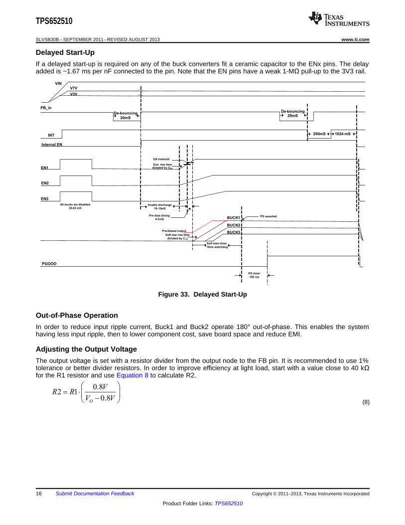
Delayed Start-UpIf a delayed start-up is required on any of the buck converters fit a ceramic capacitor to the ENx pins. The delayadded is ~1.67 ms per nF connected to the pin. Note that the EN pins have a weak 1-MΩ pull-up to the 3V3 rail.
Figure 33. Delayed Start-Up
Out-of-Phase OperationIn order to reduce input ripple current, Buck1 and Buck2 operate 180° out-of-phase. This enables the systemhaving less input ripple, then to lower component cost, save board space and reduce EMI.
Adjusting the Output VoltageThe output voltage is set with a resistor divider from the output node to the FB pin. It is recommended to use 1%tolerance or better divider resistors. In order to improve efficiency at light load, start with a value close to 40 kΩfor the R1 resistor and use Equation 8 to calculate R2.
(8)
16 Submit Documentation Feedback Copyright © 2011–2013, Texas Instruments Incorporated
Product Folder Links: TPS652510
Current Sense
I/V Gain
mgM 130=
VO
iL
CORL
RESRGm = 10 A/V
R1 Cff
FBx
R2V = 0.8 VREFCOMPx
RC
CC
CRoll
FB
0.8V
Vo
+
-
TPS652510
R1
R2
TPS652510
www.ti.com SLVSB30B –SEPTEMBER 2011–REVISED AUGUST 2013
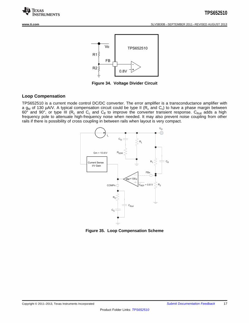
Figure 34. Voltage Divider Circuit
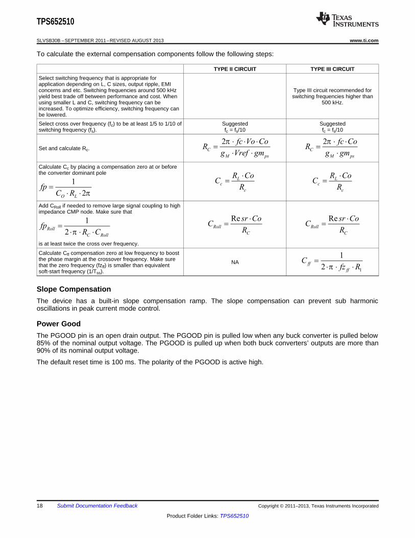
Loop CompensationTPS652510 is a current mode control DC/DC converter. The error amplifier is a transconductance amplifier witha gM of 130 µA/V. A typical compensation circuit could be type II (Rc and Cc) to have a phase margin between60° and 90°, or type III (Rc and Cc and Cff to improve the converter transient response. CRoll adds a highfrequency pole to attenuate high-frequency noise when needed. It may also prevent noise coupling from otherrails if there is possibility of cross coupling in between rails when layout is very compact.
Figure 35. Loop Compensation Scheme
Copyright © 2011–2013, Texas Instruments Incorporated Submit Documentation Feedback 17
Product Folder Links: TPS652510
1
1
2ff
ff
Cfz Rp
=× × ×
1
2Roll
C Roll
fpR Cp
=× × ×
Re
Roll
C
sr CoC
R
×=
Re
Roll
C
sr CoC
R
×=
1
2O L
fpC R p
=× ×
Lc
c
R CoC
R
×=
Lc
c
R CoC
R
×=
2C
M ps
fc Vo CoR
g Vref gm
p × × ×=
× ×
2C
M ps
fc CoR
g gm
p × ×=
×
TPS652510
SLVSB30B –SEPTEMBER 2011–REVISED AUGUST 2013 www.ti.com
To calculate the external compensation components follow the following steps:
TYPE II CIRCUIT TYPE III CIRCUITSelect switching frequency that is appropriate forapplication depending on L, C sizes, output ripple, EMIconcerns and etc. Switching frequencies around 500 kHz Type III circuit recommended foryield best trade off between performance and cost. When switching frequencies higher thanusing smaller L and C, switching frequency can be 500 kHz.increased. To optimize efficiency, switching frequency canbe lowered.Select cross over frequency (fc) to be at least 1/5 to 1/10 of Suggested Suggestedswitching frequency (fs). fc = fs/10 fc = fs/10
Set and calculate Rc.
Calculate Cc by placing a compensation zero at or beforethe converter dominant pole
Add CRoll if needed to remove large signal coupling to highimpedance CMP node. Make sure that
is at least twice the cross over frequency.
Calculate Cff compensation zero at low frequency to boostthe phase margin at the crossover frequency. Make sure NAthat the zero frequency (fzff) is smaller than equivalentsoft-start frequency (1/Tss).
Slope CompensationThe device has a built-in slope compensation ramp. The slope compensation can prevent sub harmonicoscillations in peak current mode control.
Power GoodThe PGOOD pin is an open drain output. The PGOOD pin is pulled low when any buck converter is pulled below85% of the nominal output voltage. The PGOOD is pulled up when both buck converters’ outputs are more than90% of its nominal output voltage.
The default reset time is 100 ms. The polarity of the PGOOD is active high.
18 Submit Documentation Feedback Copyright © 2011–2013, Texas Instruments Incorporated
Product Folder Links: TPS652510
TPS652510
www.ti.com SLVSB30B –SEPTEMBER 2011–REVISED AUGUST 2013
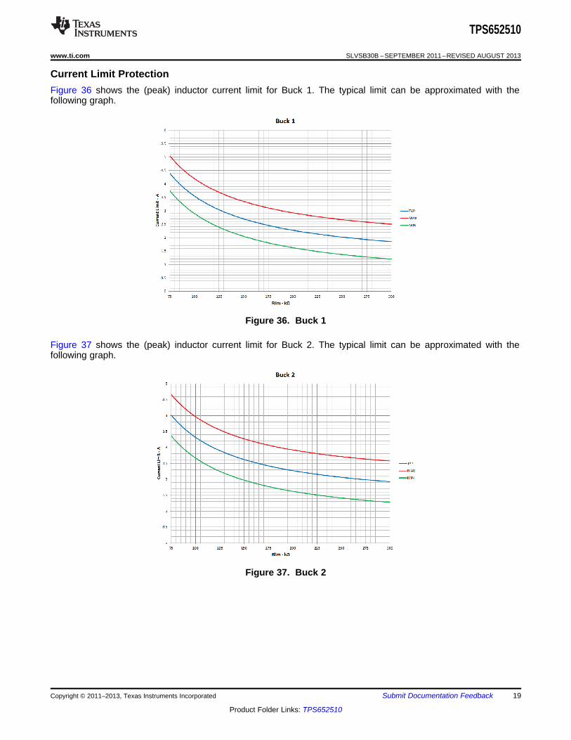
Current Limit ProtectionFigure 36 shows the (peak) inductor current limit for Buck 1. The typical limit can be approximated with thefollowing graph.
Figure 36. Buck 1
Figure 37 shows the (peak) inductor current limit for Buck 2. The typical limit can be approximated with thefollowing graph.
Figure 37. Buck 2
Copyright © 2011–2013, Texas Instruments Incorporated Submit Documentation Feedback 19
Product Folder Links: TPS652510
TPS652510
SLVSB30B –SEPTEMBER 2011–REVISED AUGUST 2013 www.ti.com
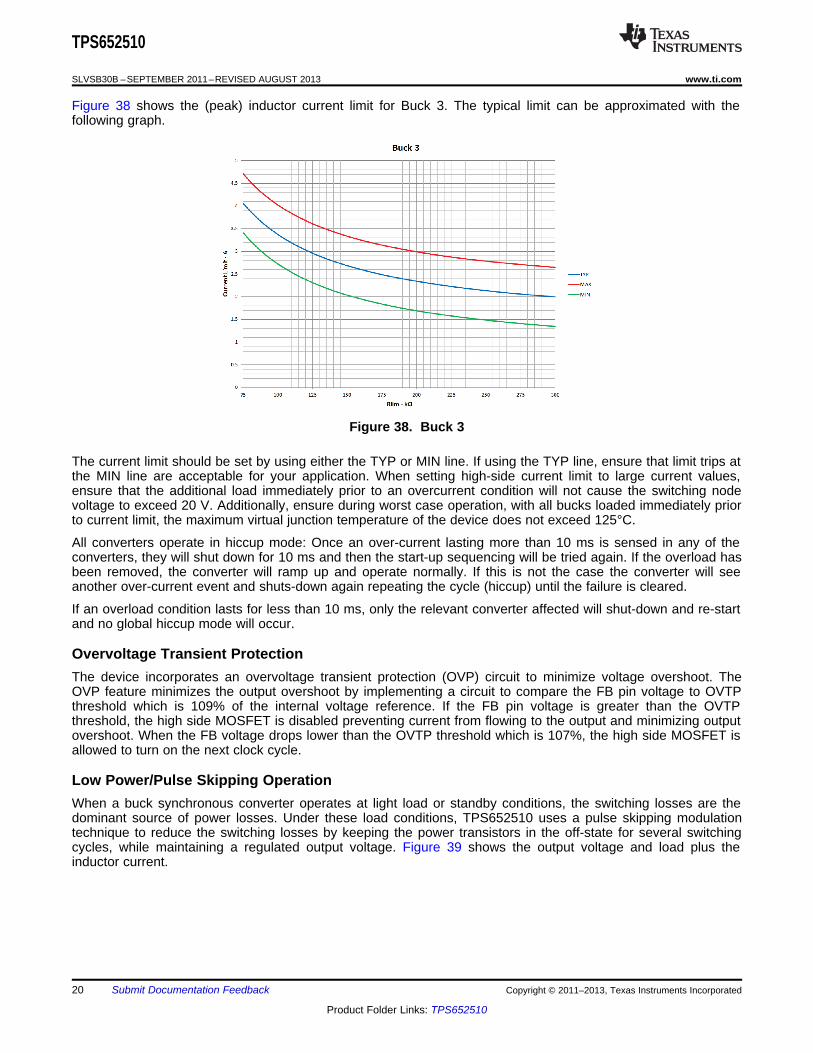
Figure 38 shows the (peak) inductor current limit for Buck 3. The typical limit can be approximated with thefollowing graph.
Figure 38. Buck 3
The current limit should be set by using either the TYP or MIN line. If using the TYP line, ensure that limit trips atthe MIN line are acceptable for your application. When setting high-side current limit to large current values,ensure that the additional load immediately prior to an overcurrent condition will not cause the switching nodevoltage to exceed 20 V. Additionally, ensure during worst case operation, with all bucks loaded immediately priorto current limit, the maximum virtual junction temperature of the device does not exceed 125°C.
All converters operate in hiccup mode: Once an over-current lasting more than 10 ms is sensed in any of theconverters, they will shut down for 10 ms and then the start-up sequencing will be tried again. If the overload hasbeen removed, the converter will ramp up and operate normally. If this is not the case the converter will seeanother over-current event and shuts-down again repeating the cycle (hiccup) until the failure is cleared.
If an overload condition lasts for less than 10 ms, only the relevant converter affected will shut-down and re-startand no global hiccup mode will occur.
Overvoltage Transient ProtectionThe device incorporates an overvoltage transient protection (OVP) circuit to minimize voltage overshoot. TheOVP feature minimizes the output overshoot by implementing a circuit to compare the FB pin voltage to OVTPthreshold which is 109% of the internal voltage reference. If the FB pin voltage is greater than the OVTPthreshold, the high side MOSFET is disabled preventing current from flowing to the output and minimizing outputovershoot. When the FB voltage drops lower than the OVTP threshold which is 107%, the high side MOSFET isallowed to turn on the next clock cycle.
Low Power/Pulse Skipping OperationWhen a buck synchronous converter operates at light load or standby conditions, the switching losses are thedominant source of power losses. Under these load conditions, TPS652510 uses a pulse skipping modulationtechnique to reduce the switching losses by keeping the power transistors in the off-state for several switchingcycles, while maintaining a regulated output voltage. Figure 39 shows the output voltage and load plus theinductor current.
20 Submit Documentation Feedback Copyright © 2011–2013, Texas Instruments Incorporated
Product Folder Links: TPS652510
0.35S
IN OUT OUT
IN
T
V V V
L V
=é ù-æ öê úç ÷è øë û
_RIP S
OUT RIPPLE
OUT
K TV
C=
VOUT
BurstSkipping
IL
IOUT
TPS652510
www.ti.com SLVSB30B –SEPTEMBER 2011–REVISED AUGUST 2013
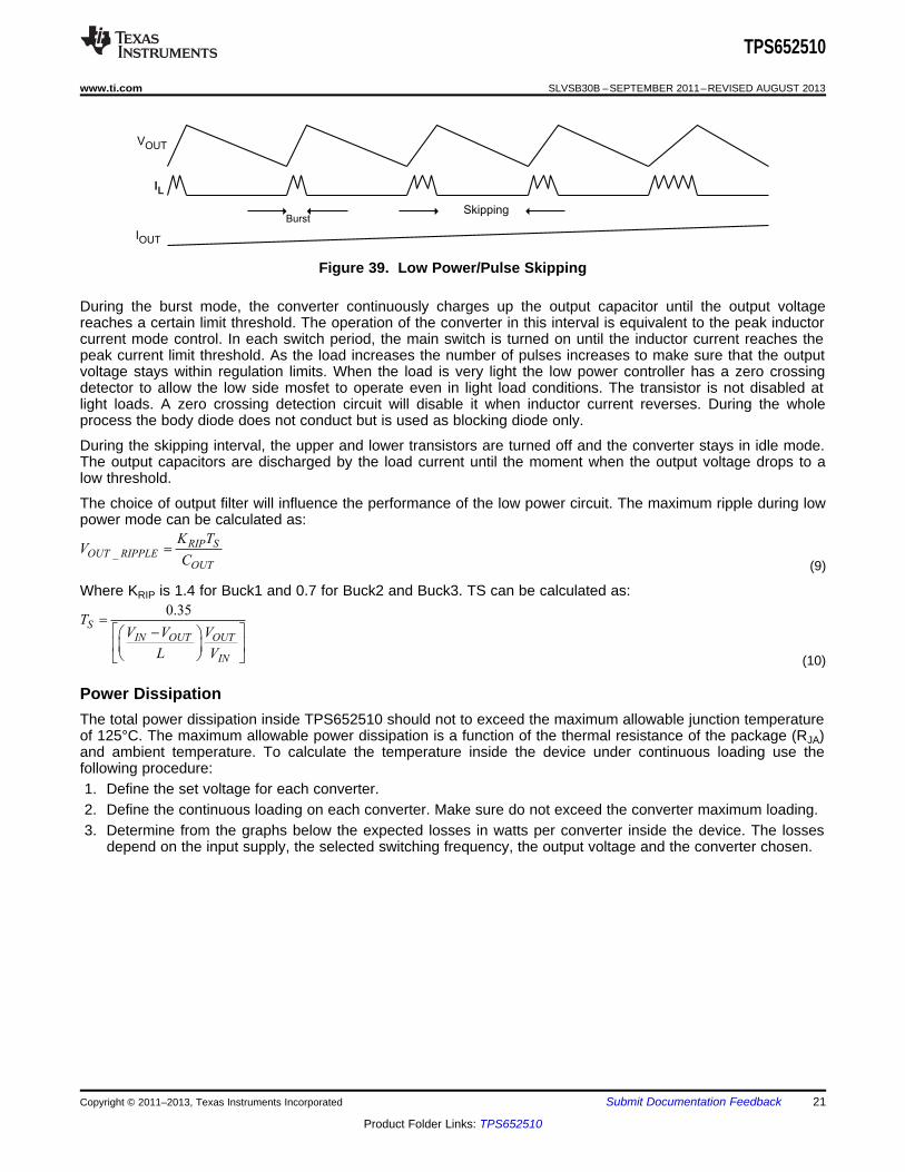
Figure 39. Low Power/Pulse Skipping
During the burst mode, the converter continuously charges up the output capacitor until the output voltagereaches a certain limit threshold. The operation of the converter in this interval is equivalent to the peak inductorcurrent mode control. In each switch period, the main switch is turned on until the inductor current reaches thepeak current limit threshold. As the load increases the number of pulses increases to make sure that the outputvoltage stays within regulation limits. When the load is very light the low power controller has a zero crossingdetector to allow the low side mosfet to operate even in light load conditions. The transistor is not disabled atlight loads. A zero crossing detection circuit will disable it when inductor current reverses. During the wholeprocess the body diode does not conduct but is used as blocking diode only.
During the skipping interval, the upper and lower transistors are turned off and the converter stays in idle mode.The output capacitors are discharged by the load current until the moment when the output voltage drops to alow threshold.
The choice of output filter will influence the performance of the low power circuit. The maximum ripple during lowpower mode can be calculated as:
(9)
Where KRIP is 1.4 for Buck1 and 0.7 for Buck2 and Buck3. TS can be calculated as:
(10)
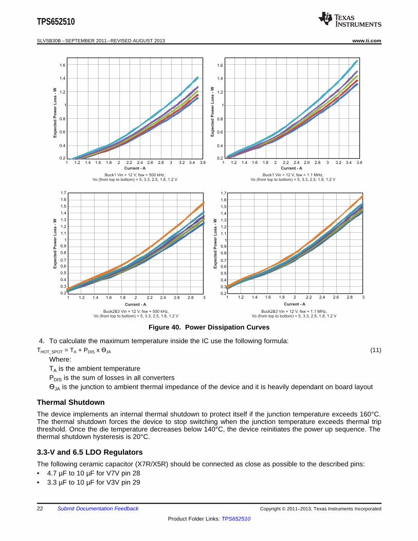
Power DissipationThe total power dissipation inside TPS652510 should not to exceed the maximum allowable junction temperatureof 125°C. The maximum allowable power dissipation is a function of the thermal resistance of the package (RJA)and ambient temperature. To calculate the temperature inside the device under continuous loading use thefollowing procedure:1. Define the set voltage for each converter.2. Define the continuous loading on each converter. Make sure do not exceed the converter maximum loading.3. Determine from the graphs below the expected losses in watts per converter inside the device. The losses
depend on the input supply, the selected switching frequency, the output voltage and the converter chosen.
Copyright © 2011–2013, Texas Instruments Incorporated Submit Documentation Feedback 21
Product Folder Links: TPS652510
0.2
0.4
0.6
0.8
1
1.2
1.4
1.6
1 1.2 1.4 1.6 1.8 2 2.2 2.4 2.6 2.8 3 3.2 3.4 3.6
Current - A
0.2
0.4
0.6
0.8
1
1.2
1.4
1.6
1 1.2 1.4 1.6 1.8 2 2.2 2.4 2.6 2.8 3 3.2 3.4 3.6
Current - A
0.2
0.3
0.4
0.5
0.6
0.7
0.8
0.9
1
1.1
1.2
1.3
1.4
1.5
1.6
1.7
1 1.2 1.4 1.6 1.8 2 2.2 2.4 2.6 2.8 3
Current - A
0.2
0.3
0.4
0.5
0.6
0.7
0.8
0.9
1
1.1
1.2
1.3
1.4
1.5
1.6
1.7
1 1.2 1.4 1.6 1.8 2 2.2 2.4 2.6 2.8 3
Current - A
Buck1 Vin = 12 V, fsw = 500 kHz,Vo (from top to bottom) = 5, 3.3, 2.5, 1.8, 1.2 V
Buck1 Vin = 12 V, fsw = 1.1 MHz,Vo (from top to bottom) = 5, 3.3, 2.5, 1.8, 1.2 V
Buck2&3 Vin = 12 V, fsw = 500 kHz,Vo (from top to bottom) = 5, 3.3, 2.5, 1.8, 1.2 V
Buck2&3 Vin = 12 V, fsw = 1.1 MHz,Vo (from top to bottom) = 5, 3.3, 2.5, 1.8, 1.2 V
Ex
pe
cte
dP
ow
er
Lo
ss
-W
Ex
pe
cte
dP
ow
er
Lo
ss
-W
Ex
pe
cte
dP
ow
er
Lo
ss
-W
Ex
pe
cte
dP
ow
er
Lo
ss
-W
TPS652510
SLVSB30B –SEPTEMBER 2011–REVISED AUGUST 2013 www.ti.com
Figure 40. Power Dissipation Curves
4. To calculate the maximum temperature inside the IC use the following formula:THOT_SPOT = TA + PDIS x ѲJA (11)
Where:TA is the ambient temperaturePDIS is the sum of losses in all convertersѲJA is the junction to ambient thermal impedance of the device and it is heavily dependant on board layout
Thermal ShutdownThe device implements an internal thermal shutdown to protect itself if the junction temperature exceeds 160°C.The thermal shutdown forces the device to stop switching when the junction temperature exceeds thermal tripthreshold. Once the die temperature decreases below 140°C, the device reinitiates the power up sequence. Thethermal shutdown hysteresis is 20°C.
3.3-V and 6.5 LDO RegulatorsThe following ceramic capacitor (X7R/X5R) should be connected as close as possible to the described pins:• 4.7 µF to 10 µF for V7V pin 28• 3.3 µF to 10 µF for V3V pin 29
22 Submit Documentation Feedback Copyright © 2011–2013, Texas Instruments Incorporated
Product Folder Links: TPS652510
TPS652510
www.ti.com SLVSB30B –SEPTEMBER 2011–REVISED AUGUST 2013
Layout RecommendationLayout is a critical portion of PMIC designs.• Place tracing for output voltage and LX on the top layer and an inner power plane for VIN.• Fit also on the top layer connections for the remaining pins of the PMIC and a large top side area filled with
ground.• The top layer ground area should be connected to the internal ground layer(s) using vias at the input bypass
capacitor, the output filter capacitor and directly under the TPS652510 device to provide a thermal path fromthe PowerPad land to ground.
• For operation at full rated load, the top side ground area together with the internal ground plane, must provideadequate heat dissipating area.
• There are several signals paths that conduct fast changing currents or voltages that can interact with strayinductance or parasitic capacitance to generate noise or degrade the power supplies performance. To helpeliminate these problems, the VIN pin should be bypassed to ground with a low ESR ceramic bypasscapacitor with X5R or X7R dielectric. Care should be taken to minimize the loop area formed by the bypasscapacitor connections, the VIN pins, and the ground connections. Since the LX connection is the switchingnode, the output inductor should be located close to the LX pins, and the area of the PCB conductorminimized to prevent excessive capacitive coupling.
• The output filter capacitor ground should use the same power ground trace as the VIN input bypass capacitor.Try to minimize this conductor length while maintaining adequate width.
• The compensation should be as close as possible to the CMPx pins. The CMPx and ROSC pins are sensitiveto noise so the components associated to these pins should be located as close as possible to the IC androuted with minimal lengths of trace.
SPACER
Copyright © 2011–2013, Texas Instruments Incorporated Submit Documentation Feedback 23
Product Folder Links: TPS652510
TPS652510
SLVSB30B –SEPTEMBER 2011–REVISED AUGUST 2013 www.ti.com
REVISION HISTORY
Changes from Revision A (September 2011) to Revision B Page
• Changed Functional Block Diagram image .......................................................................................................................... 3• Changed Terminal Function descriptions for V7V and V3V ................................................................................................. 5• Added F_PWM to Absolute Maximum Ratings .................................................................................................................... 6• Changed INPUT SUPPLY UVLO AND INTERNAL SUPPLY VOLTAGE parameters ......................................................... 7• Added I3V and I7V limits ......................................................................................................................................................... 7• Changed VIH and VIL limits .................................................................................................................................................... 7• Changed FEEDBACK, REGULATION, OUTPUT STAGE parameters ................................................................................ 7• Changed Equation 5 ........................................................................................................................................................... 15• Changed Type III Circuit description for first row ................................................................................................................ 18• Changed ............................................................................................................................................................................. 18• Changed Current Limit Protection section .......................................................................................................................... 19• Changed Figure 36 ............................................................................................................................................................. 19• Changed Figure 37 ............................................................................................................................................................. 19• Changed Figure 38 ............................................................................................................................................................. 20• Changed current limit description ....................................................................................................................................... 20• Changed Figure 40 ............................................................................................................................................................. 22• Changed 3.3-V and 6.5 LDO Regulators section ............................................................................................................... 22
24 Submit Documentation Feedback Copyright © 2011–2013, Texas Instruments Incorporated
Product Folder Links: TPS652510
PACKAGE OPTION ADDENDUM
www.ti.com 30-Apr-2013
Addendum-Page 1
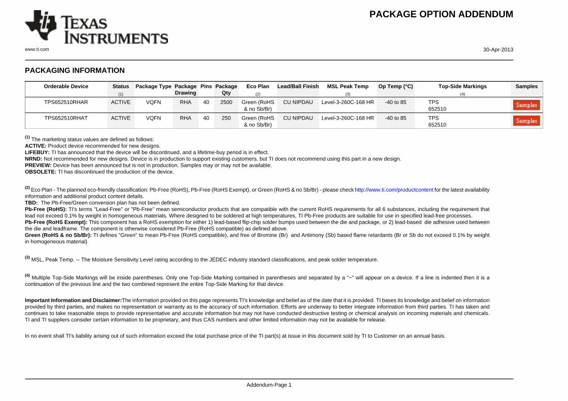
PACKAGING INFORMATION
Orderable Device Status(1)
Package Type PackageDrawing
Pins PackageQty
Eco Plan(2)
Lead/Ball Finish MSL Peak Temp(3)
Op Temp (°C) Top-Side Markings(4)
Samples
TPS652510RHAR ACTIVE VQFN RHA 40 2500 Green (RoHS& no Sb/Br)
CU NIPDAU Level-3-260C-168 HR -40 to 85 TPS652510
TPS652510RHAT ACTIVE VQFN RHA 40 250 Green (RoHS& no Sb/Br)
CU NIPDAU Level-3-260C-168 HR -40 to 85 TPS652510
(1) The marketing status values are defined as follows:ACTIVE: Product device recommended for new designs.LIFEBUY: TI has announced that the device will be discontinued, and a lifetime-buy period is in effect.NRND: Not recommended for new designs. Device is in production to support existing customers, but TI does not recommend using this part in a new design.PREVIEW: Device has been announced but is not in production. Samples may or may not be available.OBSOLETE: TI has discontinued the production of the device.
(2) Eco Plan - The planned eco-friendly classification: Pb-Free (RoHS), Pb-Free (RoHS Exempt), or Green (RoHS & no Sb/Br) - please check http://www.ti.com/productcontent for the latest availabilityinformation and additional product content details.TBD: The Pb-Free/Green conversion plan has not been defined.Pb-Free (RoHS): TI's terms "Lead-Free" or "Pb-Free" mean semiconductor products that are compatible with the current RoHS requirements for all 6 substances, including the requirement thatlead not exceed 0.1% by weight in homogeneous materials. Where designed to be soldered at high temperatures, TI Pb-Free products are suitable for use in specified lead-free processes.Pb-Free (RoHS Exempt): This component has a RoHS exemption for either 1) lead-based flip-chip solder bumps used between the die and package, or 2) lead-based die adhesive used betweenthe die and leadframe. The component is otherwise considered Pb-Free (RoHS compatible) as defined above.Green (RoHS & no Sb/Br): TI defines "Green" to mean Pb-Free (RoHS compatible), and free of Bromine (Br) and Antimony (Sb) based flame retardants (Br or Sb do not exceed 0.1% by weightin homogeneous material)
(3) MSL, Peak Temp. -- The Moisture Sensitivity Level rating according to the JEDEC industry standard classifications, and peak solder temperature.
(4) Multiple Top-Side Markings will be inside parentheses. Only one Top-Side Marking contained in parentheses and separated by a "~" will appear on a device. If a line is indented then it is acontinuation of the previous line and the two combined represent the entire Top-Side Marking for that device.
Important Information and Disclaimer:The information provided on this page represents TI's knowledge and belief as of the date that it is provided. TI bases its knowledge and belief on informationprovided by third parties, and makes no representation or warranty as to the accuracy of such information. Efforts are underway to better integrate information from third parties. TI has taken andcontinues to take reasonable steps to provide representative and accurate information but may not have conducted destructive testing or chemical analysis on incoming materials and chemicals.TI and TI suppliers consider certain information to be proprietary, and thus CAS numbers and other limited information may not be available for release.
In no event shall TI's liability arising out of such information exceed the total purchase price of the TI part(s) at issue in this document sold by TI to Customer on an annual basis.
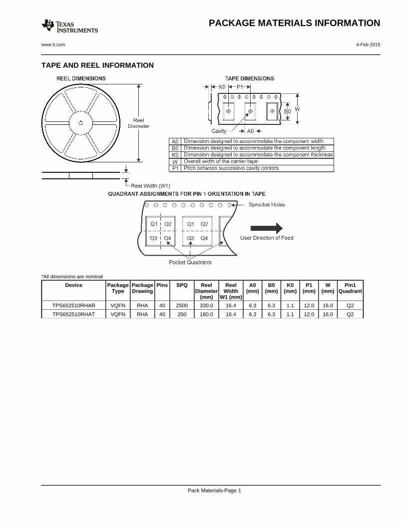
TAPE AND REEL INFORMATION
*All dimensions are nominal
Device PackageType
PackageDrawing
Pins SPQ ReelDiameter
(mm)
ReelWidth
W1 (mm)
A0(mm)
B0(mm)
K0(mm)
P1(mm)
W(mm)
Pin1Quadrant
TPS652510RHAR VQFN RHA 40 2500 330.0 16.4 6.3 6.3 1.1 12.0 16.0 Q2
TPS652510RHAT VQFN RHA 40 250 180.0 16.4 6.3 6.3 1.1 12.0 16.0 Q2
PACKAGE MATERIALS INFORMATION
www.ti.com 4-Feb-2015
Pack Materials-Page 1
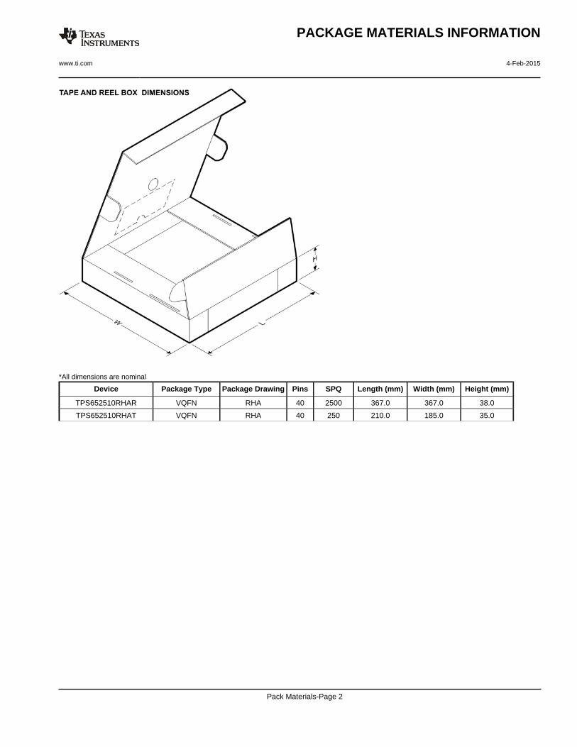
*All dimensions are nominal
Device Package Type Package Drawing Pins SPQ Length (mm) Width (mm) Height (mm)
TPS652510RHAR VQFN RHA 40 2500 367.0 367.0 38.0
TPS652510RHAT VQFN RHA 40 250 210.0 185.0 35.0
PACKAGE MATERIALS INFORMATION
www.ti.com 4-Feb-2015
Pack Materials-Page 2
IMPORTANT NOTICE
Texas Instruments Incorporated and its subsidiaries (TI) reserve the right to make corrections, enhancements, improvements and otherchanges to its semiconductor products and services per JESD46, latest issue, and to discontinue any product or service per JESD48, latestissue. Buyers should obtain the latest relevant information before placing orders and should verify that such information is current andcomplete. All semiconductor products (also referred to herein as “components”) are sold subject to TI’s terms and conditions of salesupplied at the time of order acknowledgment.TI warrants performance of its components to the specifications applicable at the time of sale, in accordance with the warranty in TI’s termsand conditions of sale of semiconductor products. Testing and other quality control techniques are used to the extent TI deems necessaryto support this warranty. Except where mandated by applicable law, testing of all parameters of each component is not necessarilyperformed.TI assumes no liability for applications assistance or the design of Buyers’ products. Buyers are responsible for their products andapplications using TI components. To minimize the risks associated with Buyers’ products and applications, Buyers should provideadequate design and operating safeguards.TI does not warrant or represent that any license, either express or implied, is granted under any patent right, copyright, mask work right, orother intellectual property right relating to any combination, machine, or process in which TI components or services are used. Informationpublished by TI regarding third-party products or services does not constitute a license to use such products or services or a warranty orendorsement thereof. Use of such information may require a license from a third party under the patents or other intellectual property of thethird party, or a license from TI under the patents or other intellectual property of TI.Reproduction of significant portions of TI information in TI data books or data sheets is permissible only if reproduction is without alterationand is accompanied by all associated warranties, conditions, limitations, and notices. TI is not responsible or liable for such altereddocumentation. Information of third parties may be subject to additional restrictions.Resale of TI components or services with statements different from or beyond the parameters stated by TI for that component or servicevoids all express and any implied warranties for the associated TI component or service and is an unfair and deceptive business practice.TI is not responsible or liable for any such statements.Buyer acknowledges and agrees that it is solely responsible for compliance with all legal, regulatory and safety-related requirementsconcerning its products, and any use of TI components in its applications, notwithstanding any applications-related information or supportthat may be provided by TI. Buyer represents and agrees that it has all the necessary expertise to create and implement safeguards whichanticipate dangerous consequences of failures, monitor failures and their consequences, lessen the likelihood of failures that might causeharm and take appropriate remedial actions. Buyer will fully indemnify TI and its representatives against any damages arising out of the useof any TI components in safety-critical applications.In some cases, TI components may be promoted specifically to facilitate safety-related applications. With such components, TI’s goal is tohelp enable customers to design and create their own end-product solutions that meet applicable functional safety standards andrequirements. Nonetheless, such components are subject to these terms.No TI components are authorized for use in FDA Class III (or similar life-critical medical equipment) unless authorized officers of the partieshave executed a special agreement specifically governing such use.Only those TI components which TI has specifically designated as military grade or “enhanced plastic” are designed and intended for use inmilitary/aerospace applications or environments. Buyer acknowledges and agrees that any military or aerospace use of TI componentswhich have not been so designated is solely at the Buyer's risk, and that Buyer is solely responsible for compliance with all legal andregulatory requirements in connection with such use.TI has specifically designated certain components as meeting ISO/TS16949 requirements, mainly for automotive use. In any case of use ofnon-designated products, TI will not be responsible for any failure to meet ISO/TS16949.
Products ApplicationsAudio www.ti.com/audio Automotive and Transportation www.ti.com/automotiveAmplifiers amplifier.ti.com Communications and Telecom www.ti.com/communicationsData Converters dataconverter.ti.com Computers and Peripherals www.ti.com/computersDLP® Products www.dlp.com Consumer Electronics www.ti.com/consumer-appsDSP dsp.ti.com Energy and Lighting www.ti.com/energyClocks and Timers www.ti.com/clocks Industrial www.ti.com/industrialInterface interface.ti.com Medical www.ti.com/medicalLogic logic.ti.com Security www.ti.com/securityPower Mgmt power.ti.com Space, Avionics and Defense www.ti.com/space-avionics-defenseMicrocontrollers microcontroller.ti.com Video and Imaging www.ti.com/videoRFID www.ti-rfid.comOMAP Applications Processors www.ti.com/omap TI E2E Community e2e.ti.comWireless Connectivity www.ti.com/wirelessconnectivity
Mailing Address: Texas Instruments, Post Office Box 655303, Dallas, Texas 75265Copyright © 2015, Texas Instruments Incorporated