three-phase three-leg three-level rectifier...most three-phase rectifiers use a diode bridge circuit...
TRANSCRIPT

CHAPTER 7 THREE-PHASE THREE-LEG THREE-LEVEL NEUTRAL POINT
CLAMPED RECTIFIER
7.1 Introduction Many inherent benefits of multilevel converters have led to their increased
interest amongst industry utilities. At present, the two most commonly used multilevel
topologies are the three-level neutral-point-clamped (NPC) [4-6] and cascaded
topologies. Multilevel converters have been attracting attention for medium-voltage and
high-power applications. The advantages of the NPC converters are improving the
waveform quality and reducing voltage stress on the power devices. The capacitor-
clamped converter is an alternate structure to obtain the multilevel waveforms on the ac
terminals. The voltage stress on the open power devices is constrained by clamping
capacitors. Series connection of full bridge converters was an alternate method to achieve
multilevel waveforms because of their modularity and simplicity of control. However, if
the voltage levels are more than three levels, the control strategy is complicated to
implement. Most three-phase rectifiers use a diode bridge circuit and a bulk storage
capacitor but it has poor power factor and high pulsation line current. Passive capacitors
and inductors have been used to form passive LC filters for eliminating current
harmonics and improving the system power factor. The drawbacks of the two-level
converters are the high voltage stress across the devices, large passive components and
192

hence due to the inherent advantages of the three-level NPC converters were proposed to
draw the sinusoidal line currents in phase with mains voltage [57-65].
Objective of the Control Scheme:
• To obtain a constant DC bus voltage.
• To balance the capacitor voltages.
• Bidirectional power flow.
• Low harmonic distortion of line current.
• To draw sinusoidal currents with unity power factor.
• To generate three voltage levels on the AC terminal voltages vac, vbc, vca .
7.2 Circuit Configuration
The proposed circuit configuration is based on the three-phase, three-leg
neutral point clamped converter shown in Figure 7.1. The converter consists of a boost
inductor Ls on the ac side, to filter the input harmonic current and achieve sinusoidal
current waveforms. Rs is the series equivalent resistor. Twelve switching devices with
rating Vdc / 2 and six clamping diodes with the rating of Vdc / 2 are used. The diodes are
used to clamp the dc-voltage. The converter also consists of two capacitors on the dc
terminal. va, vb, vc represents the phase voltages of the three-phase AC system.
In Figure 7.1 are the four switching devices for phase
A and similarly phase B and C have four switching devices.
are the six clamping diodes. are the input side resistance
ananapap SSSS 2121 ,,,
ccbbaa DDDDDD 212121 ,,,,, ss LR ,
193
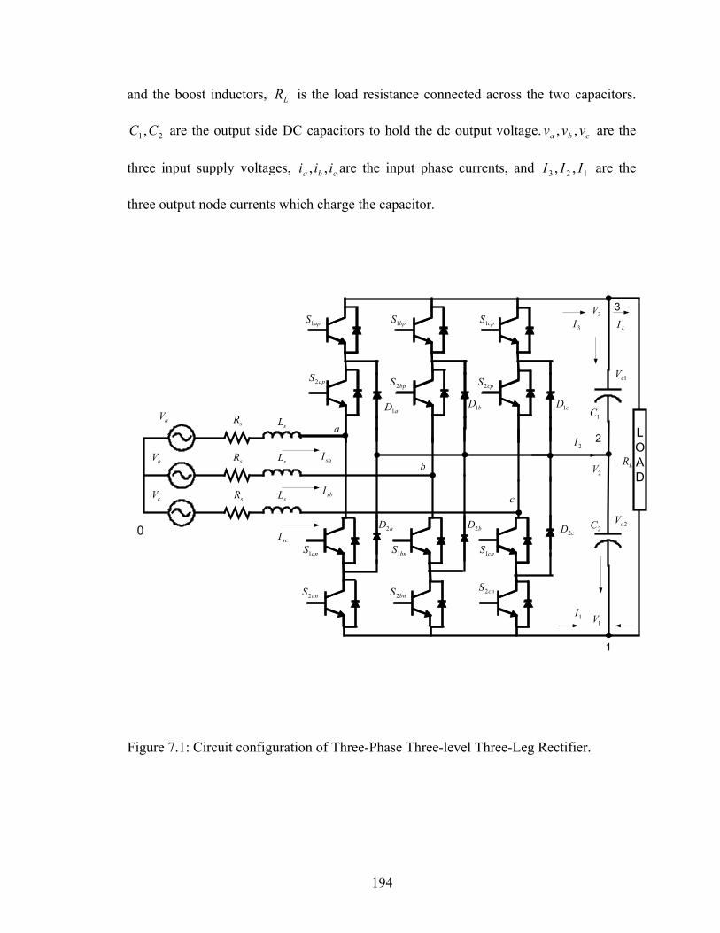
and the boost inductors, is the load resistance connected across the two capacitors.
are the output side DC capacitors to hold the dc output voltage. are the
three input supply voltages, i are the input phase currents, and are the
three output node currents which charge the capacitor.
LR
21 ,CC cba vvv ,,
123 ,, IIIcba ii ,,
0
sL
sL
sL
scI
LOAD
aV
bV
cV
sR
sR
sR
apS1
apS2
anS1
anS2
bpS1 cpS1
bpS2 cpS2
bnS1 cnS1
bnS2cnS2
aD1
aD2 bD2cD2
bD1 cD11C
2C
1cV
2cV
3I
2I
1I
LI
a
b
c
saI
sbI
3V
2V
1V
3
2
1
LR
Figure 7.1: Circuit configuration of Three-Phase Three-level Three-Leg Rectifier.
194
7.3 Modes of Operation From Chapter 3, in the operation of the multilevel converter combination of
switches are used to obtain a stepped waveform, which is close to sinusoidal waveform.
The following notations are used for certain combination of devices
ipipi
ipipi
ipipi
SSH
SSH
SSH
211
212
213
=
=
=
(7.1)
ipipipip SSSS 2211 1,1 −=−=
where i . cba ,,=
Hence in case of a three-level converter there will be three valid operating modes for
each phase of the converter as shown in Figures 7.2 –7.4. Consider Phase A as example.
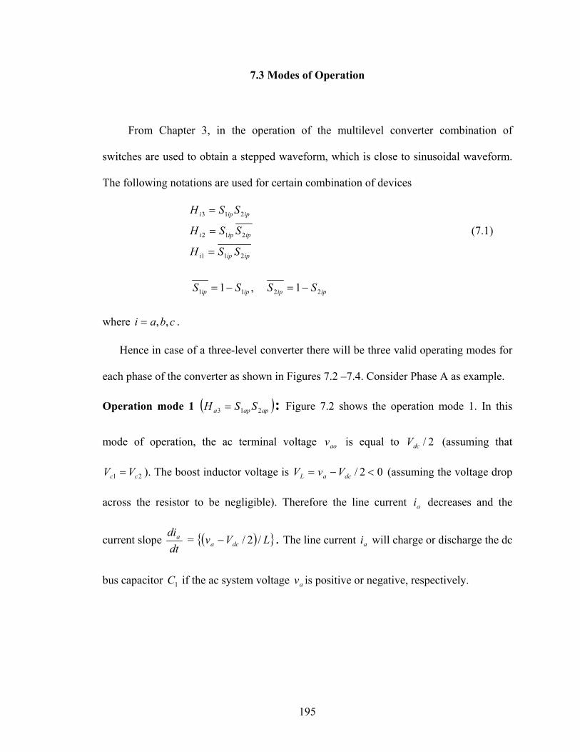
Operation mode 1 ( )apapa SSH 213 = : Figure 7.2 shows the operation mode 1. In this
mode of operation, the ac terminal voltage is equal to V (assuming that
). The boost inductor voltage is
aov 2/dc
21 cc VV = 02/ <−= dcL va VV (assuming the voltage drop
across the resistor to be negligible). Therefore the line current i decreases and the
current slope
a
dtdia
1C
= . The line current i will charge or discharge the dc
bus capacitor if the ac system voltage v is positive or negative, respectively.
( LVv dca /2/− ) a
a
195
LOADai
ao
3I
2I
1I
1cV
2cV
1C
2C
av2
1
0
aL
aov
Figure 7.2: Operational modes of the rectifier: Operation Mode 1.
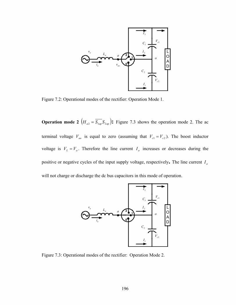
Operation mode 2 ( )apapa SSH 212 = : Figure 7.3 shows the operation mode 2. The ac
terminal voltage V is equal to zero (assuming that Vao 21 cc V= ). The boost inductor
voltage is V . Therefore the line current increases or decreases during the
positive or negative cycles of the input supply voltage, respectively. The line current
will not charge or discharge the dc bus capacitors in this mode of operation.
aL V= aI
aI
LOADai
ao
3I
2I
1I
1cV
2cV
1C
2C
av2
1
0
aL
Figure 7.3: Operational modes of the rectifier: Operation Mode 2.
196
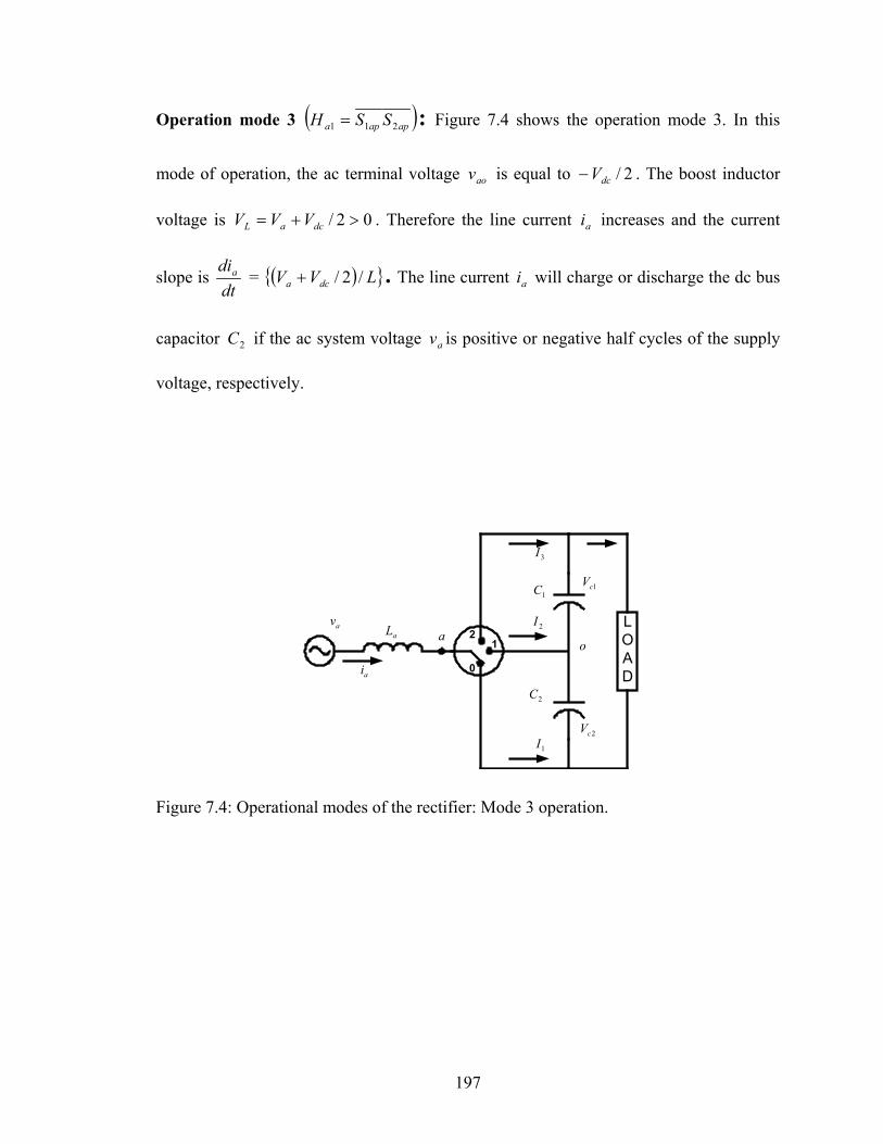
Operation mode 3 ( )apapa SSH 211 = : Figure 7.4 shows the operation mode 3. In this
mode of operation, the ac terminal voltage v is equal to ao 2/dcV− . The boost inductor
voltage is V . Therefore the line current i increases and the current
slope is
02/ >dcV+= aL V a
dtdia ( = ) LVV dca /2/+
2C
. The line current will charge or discharge the dc bus
capacitor if the ac system voltage is positive or negative half cycles of the supply
voltage, respectively.
ai
av
LOADai
ao
3I
2I
1I
1cV
2cV
1C
2C
av2
1
0
aL
Figure 7.4: Operational modes of the rectifier: Mode 3 operation.
197
7.4 Mathematical Model of the Circuit
Applying Kirchoff’s voltage law (KVL) for the input side, the supply voltage can
be written as the sum of the voltage drop across the input side impedance and
aoassaa vpiLRiv ++= (7.2)
bobssbb vpiLRiv ++= (7.3)
cocsscc vpiLRiv ++= . (7.4)
The positive node voltage appears at point ‘a’ when the upper two switching
combination occurs i.e., when are on. Hence the effective voltage that appears at
point ‘a’ in a cycle is . Similarly the other two node voltages appear when the
other switching combination occurs i.e., and . Hence the voltage v is given by
the sum of the three effective voltages
apap SS 21 ,
303VHa
2aH 1aH ao
101202303 VHVHVHv aaaao ++= (7.5)
101202303 VHVHVHv bbbbo ++= (7.6)
101202303 VHVHVHv cccco ++= . (7.7)
From Chapter 4, similar to the three-level inverter, the switching constraint to avoid
the shorting of the output capacitor; i.e., at any instant of time only one combination of
devices should be on. This leads to the condition in Eqs. (7.8-7.10)
1123 =++ aaa HHH (7.8)
1123 =++ bbb HHH (7.9)
1123 =++ ccc HHH . (7.10)
Consider phase “a”;
198
1123 =++ aaa HHH
132 1 aaa HHH −−=⇒ .
By substituting the above equation in output voltage Eq. (7.7)
( )
( ) ( )
202113
202010120303
1012013303 1
VVHVH
VVVHVVH
VHVHHVHv
caca
aa
aaaaao
+−=
+−+−=
+−−+=
where V is the voltage between the neutral of the supply to the common point of the two
capacitors.
20
Similarly for the other two phases
202113 VVHVHv cacaao +−= (7.11)
202113 VVHVHv cbcbbo +−= (7.12)
202113 VVHVHv ccccco +−= . (7.13)
By substituting the expression in Eqs. (7.11-7.13) into Eqs. (7.2-7.4)
202113 VVHVHpiLRiv cacaassaa +−++= (7.14)
202113 VVHVHpiLRiv cbcbbssbb +−++= (7.15)
202113 VVHVHpiLRiv cccccsscc +−++= . (7.16)
Hence under balanced condition,
( ) ([ ]1112333120 31
cbaccbac HHHVHHHVV +++++−= ) .
From Chapter 4, the individual device switching functions are obtained as
311
2 03
+=
d
aa V
VH ,
31
2 =aH , 311
2 01
+−=
d
aa V
VH . (7.17)
199
The switching functions of the devices can be approximated using the Fourier series.
Since the switching pulses are periodic function of time and they repeat after every cycle
of modulation signal and hence the periodic signals can be represented using the Fourier
series as a sum of dc component and sine and cosine time varying terms.
( )31133 += aa MH (7.18)
( )31122 += aa MH (7.19)
( )31111 += aa MH (7.20)
where Ma3, Ma2, Ma1 are called the modulation signal.
By equating the switching functions and Eq. (7.18)
( )311
311
2 0 +=
+ a
d
a MVv
.
Hence the modulation signal for the top devices is
d
aa V
vM 0
32
= . (7.21)
Similarly for the other devices, the modulation signal is obtained as
02 =aM and d
aa V
vM 0
12
−= . (7.22)
From Eq. (7.21) and (7.22)
. (7.23) aaa HMM =−= 13
where Ha is the modulation signal.
Substituting the modulation signals in Eqs. (7.14 – 7.17)
( ) 2021 VVVHpiLRiv ccaassaa ++++= (7.24)
200
( ) 2021 VVVHpiLRiv ccbbssbb ++++= (7.25)
( ) 2021 VVVHpiLRiv ccccsscc ++++= . (7.26)
The node currents are given by
ccbbaa iHiHiHI 3333 ++= (7.27)
ccbbaa iHiHiHI 2222 ++= (7.28)
ccbbaa iHiHiHI 1111 ++= . (7.29)
Writing the Kirchoff’s Current Law (KCL) at node 3; i.e., the current flowing through the
capacitor C is equal to the difference of the node current and the load current . The
current flowing through the capacitor is given by the KCL at node 1.
1 3I dcI
2C
ccbbaadcc iHiHiHICpV 3331 +++−= (7.30)
[ ccbbaadcc iHiHiHICpV 1112 ]+++−= (7.31)
7.5 Modeling of the Converter
Writing Eqs. (7.14-7.16) in the matrix form
202
1
1
1
1
3
3
3
000000
000000
VVHHH
VHHH
pipipi
LL
L
iii
RR
R
vvv
c
c
b
a
c
c
b
a
c
b
a
s
s
s
c
b
a
s
s
s
c
b
a
+
−
+
+
=
.
Transforming the above equation to synchronous reference frame by using transformation
matrix )(θT , where
201
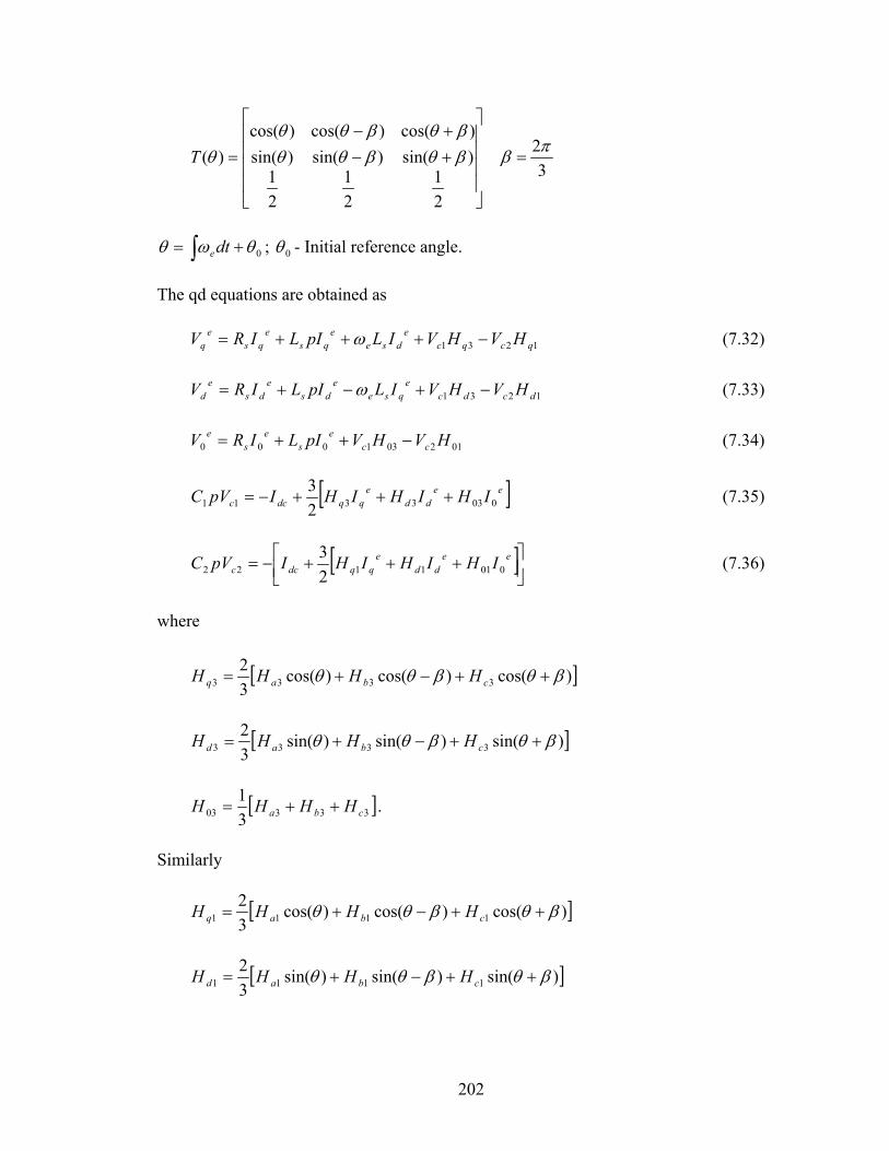
+−+−
=
21
21
21
)sin()sin()sin()cos()cos()cos(
)( βθβθθβθβθθ
θT3
2πβ =
0θωθ += ∫ dte ; 0θ - Initial reference angle.
The qd equations are obtained as
1231 qcqcedse
eqs
eqs
eq HVHVILpILIRV −+++= ω (7.32)
1231 dcdceqse
eds
eds
ed HVHVILpILIRV −+−+= ω (7.33)
012031000 HVHVpILIRV cce
se
se −++= (7.34)
[ eedd
eqqdcc IHIHIHIpVC 0033311 2
3+++−= ] (7.35)
[
+++−= ee
ddeqqdcc IHIHIHIpVC 0011122 2
3 ] (7.36)
where
[ ])cos()cos()cos(32
3333 βθβθθ ++−+= cbaq HHHH
[ ])sin()sin()sin(32
3333 βθβθθ ++−+= cbad HHHH
[ ]33303 31
cba HHHH ++= .
Similarly
[ ])cos()cos()cos(32
1111 βθβθθ ++−+= cbaq HHHH
[ ])sin()sin()sin(32
1111 βθβθθ ++−+= cbad HHHH
202
[ ]11101 31
cba HHHH ++= .
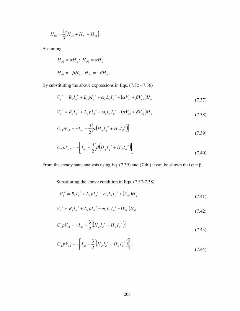
Assuming
qq HH α=3 ; dd HH α=3
qq HH β−=1 ; dd HH β−=1 .
By substituting the above expressions in Eqs. (7.32 - 7.36)
( ) qccedse
eqs
eqs
eq HVVILpILIRV 21 βαω ++++= (7.37)
( ) dcceqse
eds
eds
ed HVVILpILIRV 21 βαω ++−+= (7.38)
( )[ ]e
ddeqqdcc IHIHIpVC ++−= α
23
11 (7.39)
( )[ ] .
23
22
+−−= e
ddeqqdcc IHIHIpVC β
(7.40)
From the steady state analysis using Eq. (7.39) and (7.40) it can be shown that α = β.
Substituting the above condition in Eqs. (7.37-7.38)
( ) qdcedse
eqs
eqs
eq HVILpILIRV +++= ω (7.41)
( ) ddceqse
eds
eds
ed HVILpILIRV +−+= ω (7.42)
( )[ ]e
ddeqqdcc IHIHIpVC ++−=
23
11 (7.43)
( )[ ] .
23
22
+−−= e
ddeqqdcc IHIHIpVC
(7.44)
203
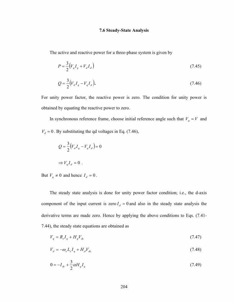
7.6 Steady-State Analysis
The active and reactive power for a three-phase system is given by
( ddqq IVIVP +=23 ) (7.45)
( dqqd IVIV −=23 )Q . (7.46)
For unity power factor, the reactive power is zero. The condition for unity power is
obtained by equating the reactive power to zero.
In synchronous reference frame, choose initial reference angle such that V Vq = and
. By substituting the qd voltages in Eq. (7.46), 0=dV
( )
.0
023
=⇒
=−=
dq
dqqd
IV
IVIVQ
But V and hence . 0≠q 0=dI
The steady state analysis is done for unity power factor condition; i.e., the d-axis
component of the input current is zero 0=dI and also in the steady state analysis the
derivative terms are made zero. Hence by applying the above conditions to Eqs. (7.41-
7.44), the steady state equations are obtained as
dcqqsq VHIRV += (7.47)
dcdqsed VHILV +−= ω (7.48)
qqdc IHI α230 +−= (7.49)
204
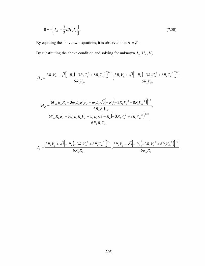
−−= qqdc IHI β
230 . (7.50)
By equating the above two equations, it is observed that βα = .
By substituting the above condition and solving for unknown dqq HHI ,,
( )[ ] ( )[ ]dcL
dcsqLLqL
dcL
dcsqLLqLq VR
VRVRRVRVR
VRVRRVRH
68333
,6
83332/1222/122 +−−++−−−
=
( )[ ]
( )[ ]dcsL
dcsqLLseqLsesLdc
dcsL
dcsqLLseqLsesLdcd
VRRVRVRRLVRLRRV
VRRVRVRRLVRLRRV
H
683336
,6
83336
2/122
2/122
+−−−+
+−−++=
ωω
ωω
( )[ ] ( )[ ]sL
dcsqLLqL
sL
dcsqLLqLq RR
VRVRRVRRR
VRVRRVRI
68333
,6
83332/1222/122 +−−−+−−+
= .
205

Figure 7.5: Plot of q-axis modulation against d-axis modulation for various dc voltages
for unity power factor operation.
206
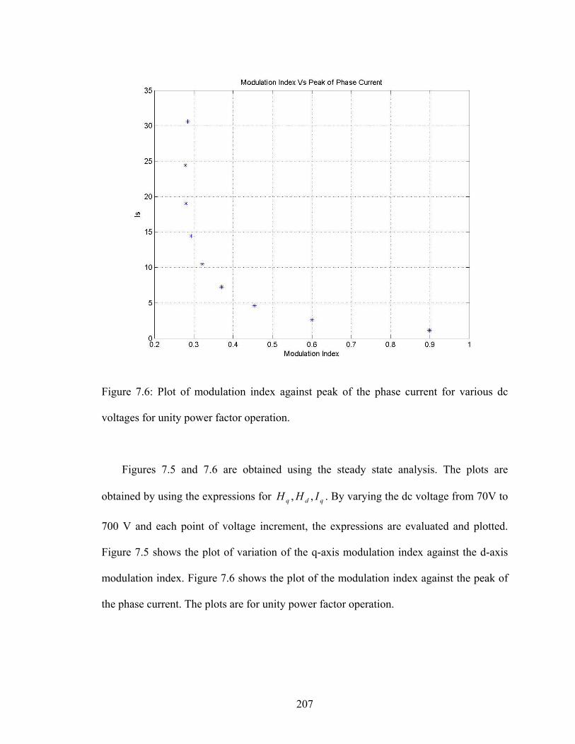
Figure 7.6: Plot of modulation index against peak of the phase current for various dc
voltages for unity power factor operation.
Figures 7.5 and 7.6 are obtained using the steady state analysis. The plots are
obtained by using the expressions for . By varying the dc voltage from 70V to
700 V and each point of voltage increment, the expressions are evaluated and plotted.
Figure 7.5 shows the plot of variation of the q-axis modulation index against the d-axis
modulation index. Figure 7.6 shows the plot of the modulation index against the peak of
the phase current. The plots are for unity power factor operation.
qdq IHH ,,
207
7.7 Open-loop Simulation of the Rectifier
From the steady-state analysis, choose a particular value of modulation index from
the plot for . Using the circuit parameters given below and using the modulation
index, the converter is simulated.
dq HH ,
7.7.1 Circuit Parameters
Input line resistance Ω= 2.0sR
Input line inductance mHLs 10=
Input Supply Voltage ( )tva ωcos80=
( )0120cos80 −= tb ωv
( )0120cos80 += tc ωv
Output dc-capacitance FCC µ220021 ==
Load resistance Ω= 75LR
In the simulation, firstly the dq modulation signals are transformed to abc
reference frame and these modulation signals are compared with the two triangles to
obtain the switching; the PWM scheme is explained in Chapter 3 and using the equations
mentioned above, the modulation scheme is implemented for unity power factor
conditions and for two different values of the dc voltages.
208
vab (a)
(b) va, ia
(c) Vc1
Vc2 (d)
(Sec)
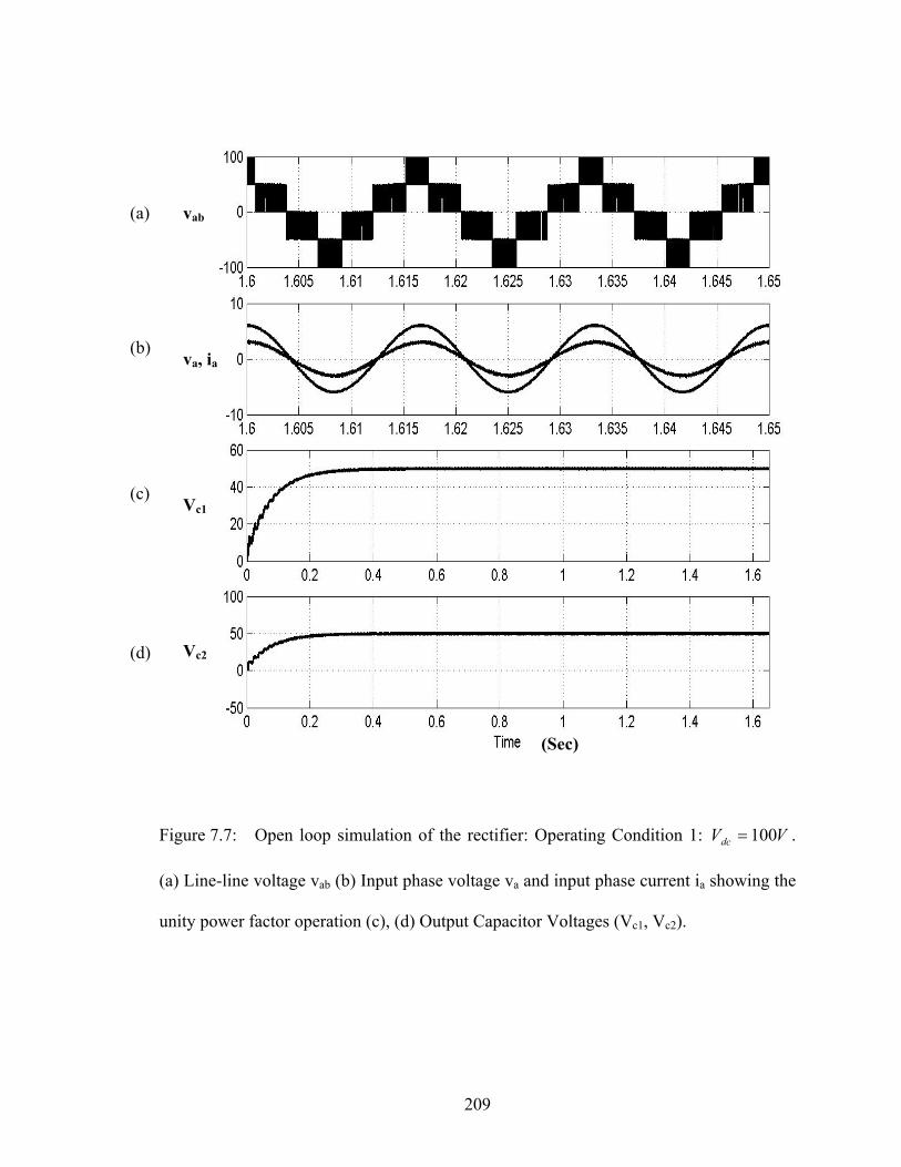
Figure 7.7: Open loop simulation of the rectifier: Operating Condition 1: V Vdc 100= .
(a) Line-line voltage vab (b) Input phase voltage va and input phase current ia showing the
unity power factor operation (c), (d) Output Capacitor Voltages (Vc1, Vc2).
209

Line
-Lin
eV
olta
ge
Pha
se “a
” Vol
tage
&P
hase
“a” C
urre
nt
Upp
er C
apac
itor
Vol
tage
Low
er C
apac
itor
Vol
tage
(a)
(b)
(c)
(d)
(Sec)
Figure 7.8: Open-loop simulation of the rectifier: Operating Condition 2: V . (a)
Line-line voltage v
Vdc 200=
ab (b) Input phase voltage va and input phase current ia showing the
unity power factor operation (c), (d) Output Capacitor Voltages (Vc1, Vc2).
210

Figure 7.7 and Figure 7.8 show the open loop simulation results for unity power
factor operation for two operating conditions. Figure 7.7 shows the simulation results for
an operating dc voltage of 100 V. Figure 7.7 (a) shows the line-to-line voltage and it
shows the steps in the voltage waveform. Figure 7.7 (b) shows the unity power factor
operation. Figure 7.7 (c) and (d) shows the two capacitor voltages and as can be seen that
the neutral point voltage is very low, in the range of 1 V. Figure 7.8 gives the simulation
results for other operating condition of Vdc = 200 V.
7.8 Control of Three-Leg Three Phase Three-Level Rectifier
The main objective of any control scheme is to regulate the actual quantity with the
reference quantity. The proposed control scheme is intended to achieve the dc-link
voltage constant, and to obtain unity power factor at the input side. Any quantity of the
system can be set as the output of the controller provided a relation as to how the
controlled quantity effects the variable taken as the output can be given, but this is
usually a tedious job.
In the control of the rectifier two methods have been proposed. Both the control
schemes are intended for the same objectives but the approach and the controllers used
are different in the two cases.
7.8.1 Control Scheme A In this particular scheme, the analysis and the control is done in a dq reference
frame; i.e., all the quantities such as the voltages, currents, etc., are transformed to
211
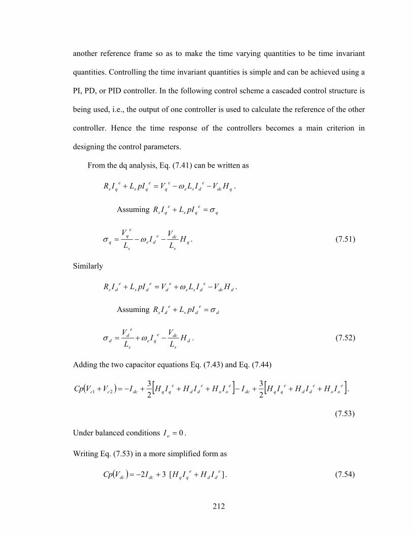
another reference frame so as to make the time varying quantities to be time invariant
quantities. Controlling the time invariant quantities is simple and can be achieved using a
PI, PD, or PID controller. In the following control scheme a cascaded control structure is
being used, i.e., the output of one controller is used to calculate the reference of the other
controller. Hence the time response of the controllers becomes a main criterion in
designing the control parameters.
From the dq analysis, Eq. (7.41) can be written as
qdcedse
eq
eqs
eqs HVILVpILIR −−=+ ω .
Assuming s IR qeqs
eq pIL σ=+
qs
dcede
s
eq
q HLV
ILV
−−= ωσ . (7.51)
Similarly
ddcedse
ed
eds
eds HVILVpILIR −+=+ ω .
Assuming s IR deds
ed pIL σ=+
ds
dceqe
s
ed
d HLV
ILV
−+= ωσ . (7.52)
Adding the two capacitor equations Eq. (7.43) and Eq. (7.44)
( ) [ ] [ ]eooedd
eqqdc
eoo
edd
eqqdccc IHIHIHIIHIHIHIVVCp +++−+++−=+
23
23
21 .
(7.53)
Under balanced conditions 0=oI .
Writing Eq. (7.53) in a more simplified form as
( ) ][32 edd
eqqdcdc IHIHIVCp ++−= . (7.54)
212
From Eqs. (7.51)-(7.52) the expression for modulation signals in qd can be obtained
dc
eqs
edesq
q V
VLILH
+−−=
ωσ (7.55)
dc
eds
eqesd
d VVLIL
H++−
=ωσ
. (7.56)
Substituting these expression in the capacitor equation
( )
++−+
+−−+−= e
ddc
eds
eqesde
qdc
eqs
edesq
dcdc IV
VLILI
VVLIL
IVCpωσωσ
32
( ) ( ) ( )[ ] .32 ed
eds
eqesd
eq
eqs
edesqdcdcdc IVLILIVLILIVCpV ++−++−−+−=⇒ ωσωσ
Assuming vdcCpV δ=2
21 .
Now arranging the terms in the above equation and simplifying
[ ] [ ] dcdcsdedsq
eq
ved
ed
eq
eq IVLILIIVIV +++=+ σσ
δ23
223
where [ ]eded
eq
eq IVIVP +=
23* .
Hence
[ dcdcsdedsq
eq
v IVLILIP +++= σσ ]δ23
2* (7.57)
where *P is the required power to meet the load.
For unity power factor operation, reactive power is zero, i.e., Q ; 0* =
The active and reactive power for a three-phase balanced system is
( ed
ed
eq
eq IVIVP +=
23* ) (7.58)
( ed
eq
eq
ed IVIVQ −=
23* ). (7.59)
By solving *P and for and *Q eqI
edI
213
[ ed
eq
eq VQVPI **
32
+∆
= ] (7.60)
[ eq
ed
ed VQVPI **
32
−∆
= ] (7.61)
where . 2*2* QP +=∆
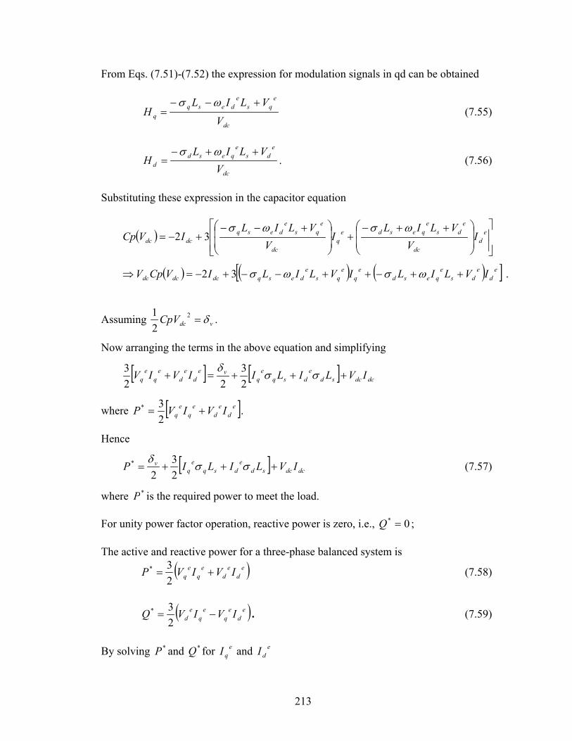
Figure 7.9 shows the schematic of the control scheme A. The voltage control is
called the outer control loop and the current controllers are the inner control loop. Hence
the time response of the current controllers has to be faster than that the voltage controller
by at least 10 times. In the control scheme the square of the actual dc voltage V is
compared with the reference dc voltage V . The error signal is passed through a PI
controller whose structure is explained in the next section. The output of this
controller is assumed as
2dc
2*dc
vK
vσ . Using expressions (7.60) and (7.61) the reference qd
currents and can be calculated. These reference currents are compared with the
actual qd currents. The errors are passed through the two current controllers and .
The outputs of these controllers are assumed as
*qI
*dI
qK dK
qσ and dσ . Using expressions (7.55) and
(7.56) the qd modulation signals can be obtained. These qd signals can be transformed
back to the abc reference frame to obtain the actual modulation signals. The carrier based
PWM is used to obtain the gating signals for the devices as explained in Chapter 3. These
modulation signals when compared with the two triangles, the switching functions for the
devices can be obtained.
214
P*,Q
*
+ -
+ - + -
Cal
cula
tion
Of
Mod
ulat
ion
Sign
als
dq/
abc
Thre
e-le
vel
rect
ifier
abc/
dq
Figu
re 7
.9 B
lock
dia
gram
of t
he c
ontro
l sch
eme
A
215
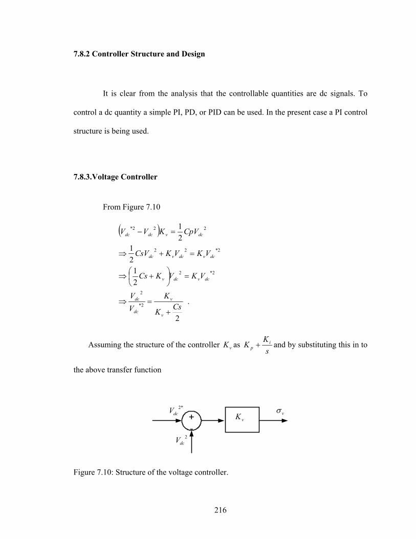
7.8.2 Controller Structure and Design It is clear from the analysis that the controllable quantities are dc signals. To
control a dc quantity a simple PI, PD, or PID can be used. In the present case a PI control
structure is being used.
7.8.3.Voltage Controller
From Figure 7.10
( )
.
2
21
21
21
2*
2
2*2
2*22
222*
CsK
KVV
VKVKCs
VKVKCsV
CpVKVV
v
v
dc
dc
dcvdcv
dcvdcvdc
dcvdcdc
+=⇒
=
+⇒
=+⇒
=−
Assuming the structure of the controller as vK sK
K ip + and by substituting this in to
the above transfer function
+-
vKvσ*2
dcV
2dcV
Figure 7.10: Structure of the voltage controller.
216
.22
2
2
2*
2
ip
ip
ip
ip
dc
dc
KsKCsKsK
CssK
K
sK
K
VV
++
+=
++
+=
One method of obtaining the controller parameters is by comparing the
denominator of the transfer function with Butter-Worth polynomial. The order of the
polynomial is same as the order of the system. The Butter-worth method locates the
Eigen values of the transfer function uniformly in the left half of the s-plane, on a circle
of radius 0ω , with its center at the origin. Hence in the present case the transfer function
is of second order system and hence the denominator is compared with the second order
Butterworth polynomial.
The second order Butter Worth polynomial is given by
02 200
2 =++ ωωss . (7.62)
Hence by comparing the coefficients of same exponentials
20ωC
K p = and 2
20ωC
Ki = . (7.63)
7.8.4 Current Controller
Using similar analysis the transfer function of the q-axis current can be obtained as
follows:
217
+-
*qsI
qsI
qKqσ
Figure 7.11: Structure of the current controller
ips
s
ip
q
q
KKLR
ss
KsK
I
I
+
++
+=
2* . (7.64)
Again the controller parameters can be obtained by comparing the denominator with
the Butterworth polynomial as
s
sp L
RK −= 02ω and . (7.65) 2
0ω=iK
As explained above the speed of the controller depends on 0ω . 0ω of current
controller should be at least ten times greater than that of the voltage controller. The d-
axis current controller has the similar kind of structure. The transfer function of the d-axis
current is
ips
s
ip
d
d
KKLR
ss
KsK
II
+
++
+=
2* . (7.66)
218
(a) vab
(b) va, ia
Vc1 (c)
Vc2 (d)
(sec)
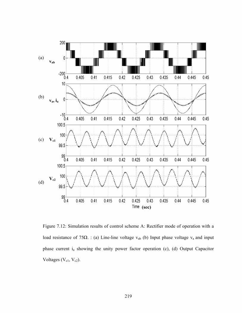
Figure 7.12: Simulation results of control scheme A: Rectifier mode of operation with a
load resistance of 75Ω. : (a) Line-line voltage vab (b) Input phase voltage va and input
phase current ia showing the unity power factor operation (c), (d) Output Capacitor
Voltages (Vc1, Vc2).
219
(a) Ha
(b) Hb,
(c) Hc
100
50
0(d)
Fi
inv
sig
fro
Load change
-50
-100
-150 Time (sec)
gure 7.13: Modulation signals during the transition from rectifier mode of operation to
erter mode of operation. (a) Phase a modulation signal (Ha) (b) Phase b modulation
nal (Hb) and (c) Phase c modulation signal (Hc). (d) Plot showing change in load i.e.,
m the rectifier mode of operation to inverter mode of operation at t = 0.6 sec.
220
vab (a)
va, ia (b)
(c) Vc1
Vc2 (d)
(sec)
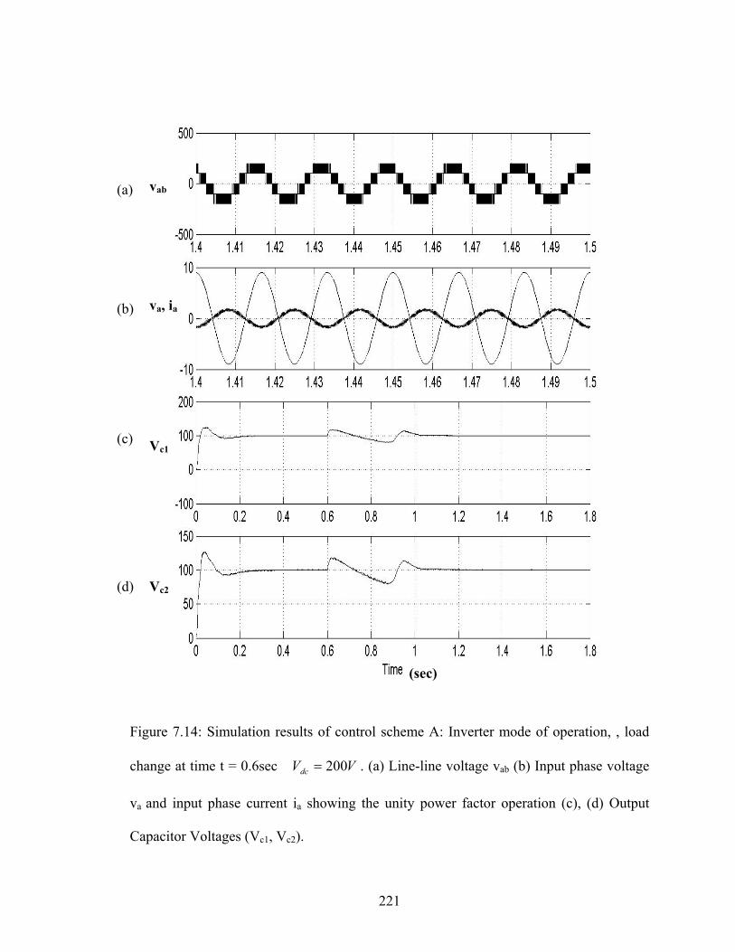
Figure 7.14: Simulation results of control scheme A: Inverter mode of operation, , load
change at time t = 0.6sec V Vdc 200= . (a) Line-line voltage vab (b) Input phase voltage
va and input phase current ia showing the unity power factor operation (c), (d) Output
Capacitor Voltages (Vc1, Vc2).
221
Vdc*, Vdc
(sec)
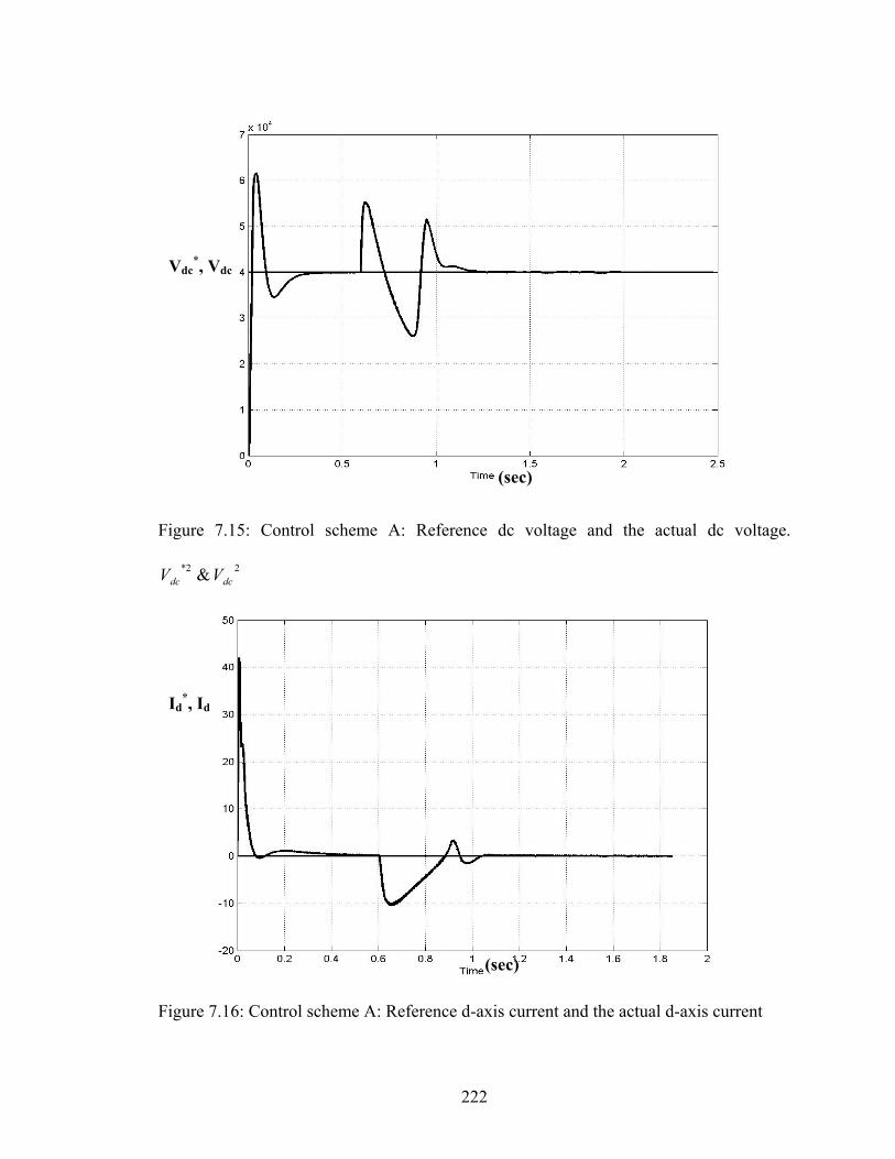
Figure 7.15: Control scheme A: Reference dc voltage and the actual dc voltage.
22* & dcdc VV
Id*, Id
(sec)
Figure 7.16: Control scheme A: Reference d-axis current and the actual d-axis current
222
Iq*, Iq
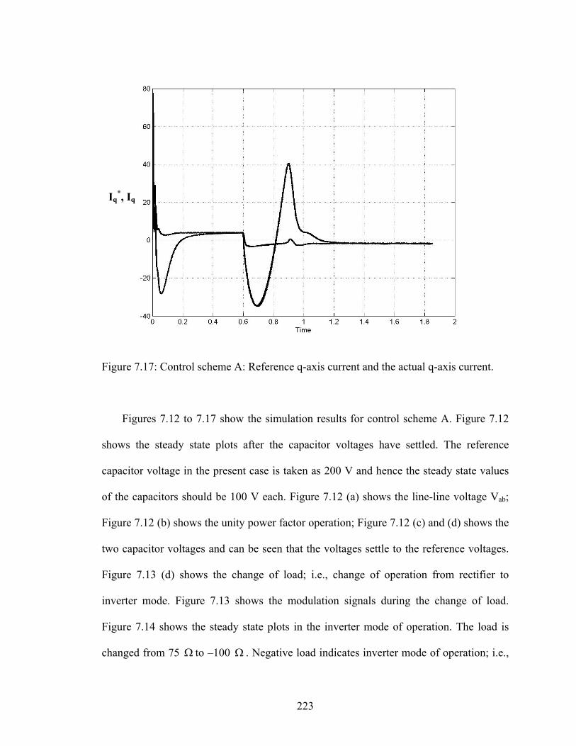
Figure 7.17: Control scheme A: Reference q-axis current and the actual q-axis current.
Figures 7.12 to 7.17 show the simulation results for control scheme A. Figure 7.12
shows the steady state plots after the capacitor voltages have settled. The reference
capacitor voltage in the present case is taken as 200 V and hence the steady state values
of the capacitors should be 100 V each. Figure 7.12 (a) shows the line-line voltage Vab;
Figure 7.12 (b) shows the unity power factor operation; Figure 7.12 (c) and (d) shows the
two capacitor voltages and can be seen that the voltages settle to the reference voltages.
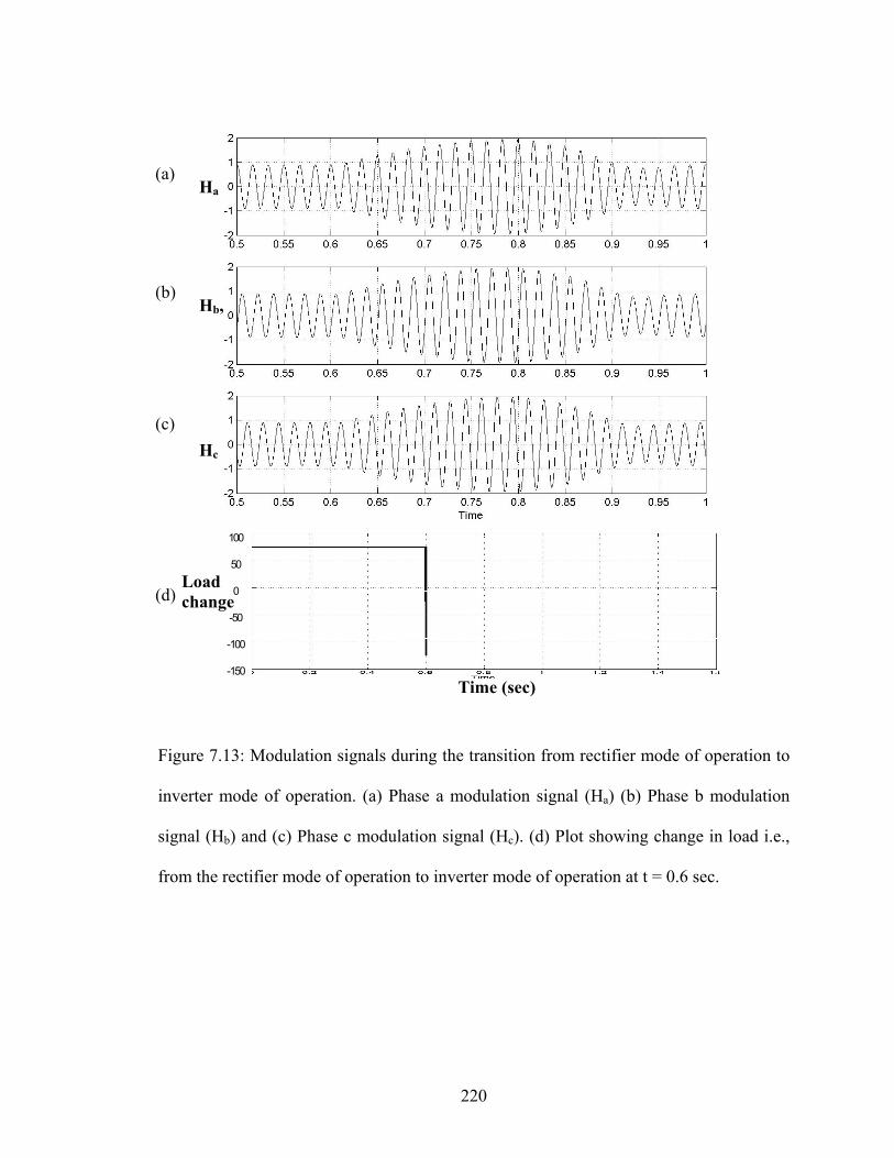
Figure 7.13 (d) shows the change of load; i.e., change of operation from rectifier to
inverter mode. Figure 7.13 shows the modulation signals during the change of load.
Figure 7.14 shows the steady state plots in the inverter mode of operation. The load is
changed from 75 Ω to –100 Ω . Negative load indicates inverter mode of operation; i.e.,
223
the power is fed back to the supply. As seen from the results, the control scheme works
effectively even in the inverter mode of operation as it achieves the capacitor voltage
control and also the unity power factor operation even in the inverter mode. Figure 7.15
shows the tracking of the capacitor voltages. It can be seen that there are some dips
because of the load change and also initially it took some time to settle to the reference
voltage. Figure 7.16 shows the tracking of the d-axis current. For unity power factor
operation d-axis component has to be zero and it is clear from the plot that d-axis current
is tracked well. Figure 7.17 shows the tracking active component of the current or the q-
axis current.
7.8.5 Control Scheme B In the previous control scheme A, the analysis is in qd reference frame; i.e., all
the quantities are transformed to synchronous reference frame so as to make the
quantities time invariant. The control structure is simple in case of the dc quantities, but
when it comes to implementation it becomes complex. Because all the quantities should
be transformed to synchronous reference frame and after that again the modulation
signals have to be transformed back to abc reference. Hence a new control scheme is
being formulated using the natural variables; i.e., control the actual signals without any
transformation. Hence the control becomes simple.
20VVHpiLRiv dcaassaa +++= (7.67)
20VVHpiLRiv dcbbssbb +++= (7.68)
224
20VVHpiLRiv dcccsscc +++= . (7.69)
For a balanced case, ( )bac iii +−= .
By substituting in Eq. (7.69) cI
( ) ( ) 20VVHiipLRiiv dccbassbac +++−+−= .
To eliminate the term V , subtract Eqs. (7.67), (7.69) and Eqs. (7.67), (7.69) 20
v dcacbssbassaac VHpiLRipiLRi ++++= 22 (7.70)
dcbcassabssbbc VHpiLRipiLRiv ++++= 22 . (7.71)
Solving for and as pIL bs pIL
sadcacdcbcacbc
as RIVHvHvv
piL −−++−
=3
22.
Rearranging the terms and simplifying
( ) dcacdcbcacbcassa VHVHvvpiLRi 223 −++−=+ .
Assuming ( )assaa piLRi += 3σ .
Hence
dcacdcbcacbca VHVHvv 22 −++−=σ . (7.72)
Similarly
dcbcdcacbcacb VHVHvv 22 −++−=σ . (7.73)
From the above Eqs. (7.72) and (7.73), solving for bcac HH ,
dc
abacac V
vH
323 σσ −−
= (7.74)
dc
babcbc V
vH
323 σσ −−
= . (7.75)
225
The capacitor equation is
CpV ccbbaadcdc iHiHiHI 2222 +++−= . (7.76)
Again substituting for cI
CpV bbcaacdcdc iHiHI 222 ++−= . (7.77)
By substituting the expressions for from Eqs. (7.74)-(7.75) bcac HH ,
bdc
babca
dc
abacdcdc i
Vv
iV
vI
−−+
−−+−=
323
23
2322
σσσσCpV . (7.78)
By simplifying the equation and writing in terms of the phase voltages
( ) ( ) .424266623 2
bbabaabacbbcaadcdcdc iiiivvivvIVICpV σσσσ −−−−−+−+−=
(7.79)
For unity power factor operation
i and i . aa Kv= bb Kv=
Hence substituting the above condition in Eq. (7.79) and simplifying
( )[ ]bcbacacbadcdcdc vvvvvKVICpV σσ 226623 2222 −−+++−= .
Assuming vdcCpV σ=2
23 and solving for value of K
∆
+= dcdcv VI
K6σ
. (7.80)
where ( )[ ]bcbacacba vvvvv σσ 226 222 −−++=∆ .
Hence the reference frame currents can be calculated as
.*
*
bb
aa
Kvi
Kvi
=
=
226
Cal
cula
tion
Of K
+ -
+ - + -
Cal
cula
tion
Of
Mod
ulat
ion
Sig
nals
Thre
e-Le
vel
Rec
tifie
r
Cal
cula
tion
Of
Ref
eren
ceC
urre
nts
Figu
re 7
.18:
Blo
ck d
iagr
am o
f the
con
trol s
chem
e B
227

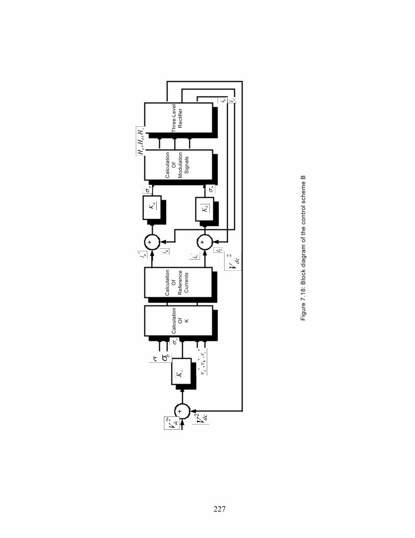
Figure 7.18 shows the schematic of the control scheme B. Similar to control
scheme A, scheme B also has the voltage control called the outer control loop and the
current controllers as the inner control loop. Hence the time response of the current
controllers has to be faster than the voltage controller at least by 10 times. In the control
scheme the square of the actual dc voltage V is compared with the reference dc voltage
. The error signal is passed through a PI controller whose structure is explained
in the next section. The output of this controller is assumed as
2dc
2*dcV vK
vσ . Using expression
(7.80) the value of K is calculated and thereby the reference currents and can be
calculated. These reference currents are compared with the actual currents. The errors are
passed through the two current controllers and . The output of these controllers is
assumed as
*ai
*bi
aK bK
aσ and bσ . Using expressions (7.74) and (7.75) the modulation signals can
be obtained.
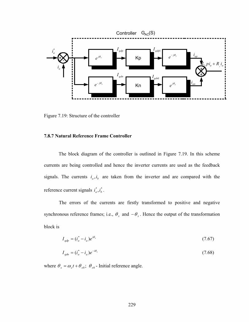
7.8.6 Controller Structure and Design It is clear that the controllable quantities are dc signal in case of voltage and ac
signals in case of currents. Hence in the control of ac quantity a simple PI, PD, or PID
cannot be used. Hence a new controller called natural reference frame controller is being
used.
228
Kp
Kn
xje θ
xje θ−
yje θ−
yje θ
Controller
*ai
ai
api
ani
aas iRpiLs
+
qdpI
qdnI
1qdpI
1qdnI
+ -
++
G (S)AC
Figure 7.19: Structure of the controller
7.8.7 Natural Reference Frame Controller
The block diagram of the controller is outlined in Figure 7.19. In this scheme
currents are being controlled and hence the inverter currents are used as the feedback
signals. The currents are taken from the inverter and are compared with the
reference current signals i .
ba ii ,
* ,a i*b
The errors of the currents are firstly transformed to positive and negative
synchronous reference frames; i.e., xθ and xθ− . Hence the output of the transformation
block is
(7.67) xiaaqdp eiiI θ)( * −=
xiaaqdn eiiI θ−−= )( * (7.68)
where ;0xex t θωθ += 0xθ - Initial reference angle.
229
After transformation the output signals are dc quantities. The signals are passed
through these controllers whose transfer function is given by Kp (p) and Kn (p). Hence the
output of the regulators is
(7.69) )()( *1 pKeiiI p
iaaqdp
xθ−=
)()( * pKeiiI ni
aaqdnxθ−−= . (7.70)
Now these signals are again transformed back to the abc reference frame with some
delay angle ; i.e., 1φ 1010 , φθωθφθωθ −+−=−+= xeyxey tt . Hence the resulting signals
from these transformation blocks are
i . (7.70) )()( )(* ωθθ jpKeii pi
aaapyx −−= −
. (7.71) )()( )(* ωθθ jpKeiii ni
aaanyx +−= −−
Let 1φθθ =− yx ; then
(7.72) )()( 1* ωφ jpKeiii pi
aaap −−=
)()( 1* ωφ jpKeiii ni
aaan +−= − . (7.73)
Now take the sum of the two signals iap, ian to get the output of the controller, which is
equal to 3 . ( )asas piLiR +
( )
)]()()[(
)()()()(3
11
11
*
**
ωω
ωω
φφ
φφ
jpKejpKeii
jpKeiijpKeiipiLiR
ni
pi
aa
ni
aapi
aaasas
++−−=
+−+−−=+
−
−
By simplifying the above equation the transfer function of the system is obtained as
)()(33
)()(11
11
* ωωωω
φφ
φφ
jpKejpKepLRjpKejpKe
ii
ni
pi
ss
ni
pi
a
a
++−++
++−= −
−
. (7.74)
230
In this particular case assume the controller to be a PI controller whose transfer function
is given as
.)(
)(
pk
kpK
pk
kpK
innn
ippp
+=
+= (7.75)
Hence, by substituting the above transfer functions in (7.67) and simplifying,
( ) .])()[(])()[()(33
])()[(])()[(11
11
22inn
iipp
iss
inni
ippi
kjpkjpekjpkjpeppLRkjpkjpekjpkjpe
++−++−++++
++−++−+= −
−
ωωωωωωωωω
φφ
φφ
*a
a
ii
For simplicity, if k ppniinip kkkkk ==== ; , then
[ ] .sin2cos23]3cos2[3cos23
sin2cos2cos2cos2
12
122
1123
12
1112
* φωωφωωφφφωωφφφ
ipssisps
ipip
a
a
kkRLkpRkppLkkkpkp
ii
−++++++
−++=
Similar analysis can be done for the phase B current and transfer function is obtained as
[ ] .sin2cos23]3cos2[3cos23
sin2cos2cos2cos2
12
122
1123
12
1112
* φωωφωωφφφωωφφφ
ipssisps
ipip
b
b
kkRLkpRkppLkkkpkp
ii
−++++++
−++=
In designing the parameters of the controller, compare the denominator of the transfer
function with Butterworth Polynomial. The Butter-worth polynomial for the third order is
as follows:
022 30
200
23 =+++ wpwwpp . (7.76)
Hence by comparing the denominator of the transfer function with above polynomial
01 2
3cos23
ωφ
=+
s
ps
LkR
(7.77)
231
20
12
23
cos23ω
φω=
+
s
is
LkL
(7.78)
30
12
12
3sin2cos23
ωφωωφω
=−+
s
ips
LkkR
. (7.79)
Hence by solving the above three equations for the three unknowns 0,, ωpi kk and by
varying the delay angle 1φ the controller parameters can be calculated.
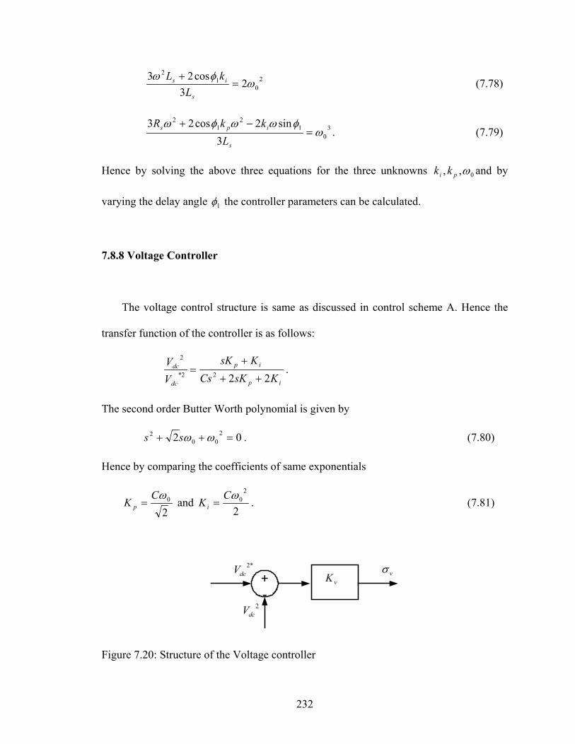
7.8.8 Voltage Controller
The voltage control structure is same as discussed in control scheme A. Hence the
transfer function of the controller is as follows:
ip
ip
dc
dc
KsKCsKsK
VV
2222*
2
++
+= .
The second order Butter Worth polynomial is given by
02 200
2 =++ ωωss . (7.80)
Hence by comparing the coefficients of same exponentials
20ωC
K p = and 2
20ωC
Ki = . (7.81)
+-
vKvσ*2
dcV
2dcV
Figure 7.20: Structure of the Voltage controller
232
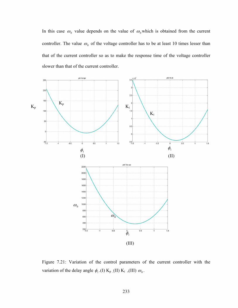
In this case 0ω value depends on the value of 0ω which is obtained from the current
controller. The value 0ω of the voltage controller has to be at least 10 times lesser than
that of the current controller so as to make the response time of the voltage controller
slower than that of the current controller.
Kp Kp Ki
Ki
1φ
1φ
0ω
Figure 7.21: Varia
variation of the del
(I)
1φ
0ω
(III)
tion of the control parameters of the curre
ay angle 1φ .(I) Kp ,(II) Ki ,(III) 0ω .
233
(II)
nt controller with the
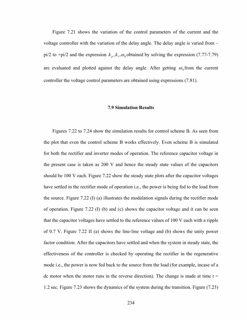
Figure 7.21 shows the variation of the control parameters of the current and the
voltage controller with the variation of the delay angle. The delay angle is varied from –
pi/2 to +pi/2 and the expression 0,, ωip kk obtained by solving the expression (7.77-7.79)
are evaluated and plotted against the delay angle. After getting 0ω from the current
controller the voltage control parameters are obtained using expressions (7.81).
7.9 Simulation Results
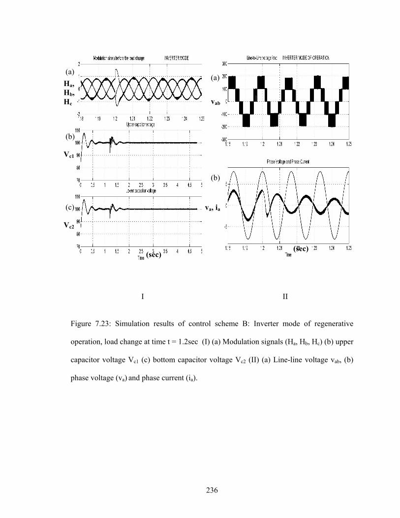
Figures 7.22 to 7.24 show the simulation results for control scheme B. As seen from
the plot that even the control scheme B works effectively. Even scheme B is simulated
for both the rectifier and inverter modes of operation. The reference capacitor voltage in
the present case is taken as 200 V and hence the steady state values of the capacitors
should be 100 V each. Figure 7.22 show the steady state plots after the capacitor voltages
have settled in the rectifier mode of operation i.e., the power is being fed to the load from
the source. Figure 7.22 (I) (a) illustrates the modulation signals during the rectifier mode
of operation. Figure 7.22 (I) (b) and (c) shows the capacitor voltage and it can be seen
that the capacitor voltages have settled to the reference values of 100 V each with a ripple
of 0.7 V. Figure 7.22 II (a) shows the line-line voltage and (b) shows the unity power
factor condition. After the capacitors have settled and when the system in steady state, the
effectiveness of the controller is checked by operating the rectifier in the regenerative
mode i.e., the power is now fed back to the source from the load (for example, incase of a
dc motor when the motor runs in the reverse direction). The change is made at time t =
1.2 sec. Figure 7.23 shows the dynamics of the system during the transition. Figure (7.23)
234
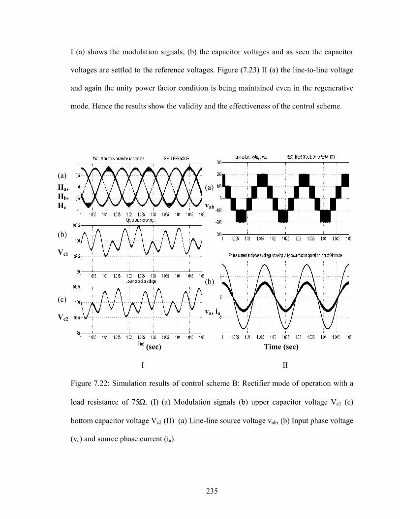
I (a) shows the modulation signals, (b) the capacitor voltages and as seen the capacitor
voltages are settled to the referenc
and again the unity power factor
mode. Hence the results show the
(a) Ha, Hb, Hc
Vc1
Vc2
(sec)
I
Figure 7.22: Simulation results of
load resistance of 75Ω. (I) (a) M
bottom capacitor voltage Vc2 (II)
(va) and source phase current (ia).
e voltages. Figure (7.23) II (a) the line-to-line voltage
condition is being maintained even in the regenerative
validity and the effectiveness of the control scheme.
vab
(b)
(c)
contro
odulati
(a) Line
(b)
(a)
va, ia
Time (sec)
II
l scheme B: Rectifier mode of operation with a
on signals (b) upper capacitor voltage Vc1 (c)
-line source voltage vab, (b) Input phase voltage
235
Ha, Hb, Hc vab
(b)Vc1
va, ia
(c)Vc2
(sec)
I Figure 7.23: Simulation results of contro
operation, load change at time t = 1.2sec (I
capacitor voltage Vc1 (c) bottom capacitor
phase voltage (va) and phase current (ia).
2
(a)
(b)
(sec)
II
l scheme B: Inverter mode of regenerative
) (a) Modulation signals (Ha, Hb, Hc) (b) upper
voltage Vc2 (II) (a) Line-line voltage vab, (b)
36
ia*, ia
(sec)
Figure 7.24: Tracking of the phase currents. Reference phase current and the actual phase
current.
237