through the wall ultra wideband radarcradpdf.drdc-rddc.gc.ca/pdfs/unc17/p520580.pdf · for a...
TRANSCRIPT
Through the Wall Ultra Wideband Radar An Investigation into the Feasibility of Building an In-House UWB Radar Hardware Capability Robert Robinson RWR Consulting
Defence R&D Canada - Ottawa CONTRACT DOCUMENT DRDC Ottawa CR 2003-023
March 2003

Copy No: _________
Through the Wall Ultra Wideband Radar An Investigation into the Feasibility of Building an In-House UWB Radar Hardware Capability
Robert Robinson RWR Consulting
The scientific or technical validity of this report is entirely the responsibility of the contractor and the contents do not necessarily have the approval or endorsement of Defence R&D Canada.
Defence R&D Canada - Ottawa Contract Document DRDC – Ottawa CR-2003-023 2004-01-06

© Her Majesty the Queen as represented by the Minister of National Defence, 2003
© Sa majesté la reine, représentée par le ministre de la Défense nationale, 2003

CR 2003-023 i
Abstract
An investigation into the feasibility of producing in-house ultra wideband (UWB) radar for experimental purposes was undertaken. The principal purpose for this system will be for through the wall radar imaging. Several architectures were examined and the most promising avenues were explored further. Wherever possible off-the-shelf components were selected to shorten the development time and costs associated with a new technology such as UWB radar. For each challenging area a potential solution is put forward and a complete system could be produced for the single transmit and receive case by the end of this year. The solutions proposed lend themselves to a modular approach and could be scaled-up to produce a multiple transmit and receive radar system with little difficulty.

This page intentionally left blank.

CR 2003-023 iii
Executive summary
Ultra wideband radar (UWB) technology has been around for about thirty years but more as a curiosity rather than a workable solution as the technology is just becoming available to support the concept. The attraction of an UWB system is its simplicity; it lacks many of the usual components found in modern radar systems such as down converters, local oscillators, mixers, etc. It is a base-band radar using a simple impulse generator for the RF source and high-speed analogue to digital converters for the receiver chain. An added advantage is its ability to penetrate many common construction materials such as building partitions, snow, and ground to name a few. The capacity to make many materials relatively transparent is due to the broad-band nature of the transmitted pulses.
The feasibility of producing in-house ultra wideband (UWB) radar for experimental purposes was undertaken to test the various merits of this type of system. Several architectures were examined and the most promising avenues were explored further. Wherever possible off-the-shelf components were selected to shorten the development time and costs associated with a new technology such as UWB radar. Practical solutions are put forward and a complete system as described that could be produced for the single transmit and receive case by the end of this year. The system is designed with a modular approach and could be scaled-up to produce multiple transmit and receive channels with little difficulty.
Robinson, R.W. 2003. Ultra Wideband Radar CR-2002-023 DRDC Ottawa.

This page intentionally left blank

CR 2003-023 v
Table of contents
Abstract........................................................................................................................................ i
Executive summary ................................................................................................................... iii
Table of contents ........................................................................................................................ v
List of figures ........................................................................................................................... vii
1. Ultra Wideband Radar System Overview ..................................................................... 9
2. Time and Distance Requirements................................................................................ 11
3. Antenna Considerations............................................................................................... 14 3.1 Experimental Antenna .................................................................................... 15
4. Impulse Generation ..................................................................................................... 18
5. Analogue to Digital Conversion .................................................................................. 20
6. Sampling Network and Timing ................................................................................... 25
7. Discussion ................................................................................................................... 29
References ................................................................................................................................ 31
List of symbols/abbreviations/acronyms/initialisms ................................................................ 32
Glossary.................................................................................................................................... 33

This page intentionally left blank

CR 2003-023 vii
List of figures
Figure 1. UWB Block Diagram.................................................................................................. 9
Figure 2. UWB Time to Distance............................................................................................. 12
Figure 3. Pulsar Output............................................................................................................. 13
Figure 4. Bowtie Antenna Dimensions..................................................................................... 15
Figure 5. Bowtie Antenna Impedance ...................................................................................... 16
Figure 6. Step Recovery Diode Idealized Response................................................................. 18
Figure 7. Step Recovery Diode Matching Network ................................................................. 19
Figure 8. Sample Rate and Distance Resolution ...................................................................... 20
Figure 9. Real Time Sampling.................................................................................................. 21
Figure 10. Equivalent Time Sampling...................................................................................... 22
Figure 11. Hybrid Sampling System ........................................................................................ 24
Figure 12. Typical Mixer Schematic ........................................................................................ 25
Figure 13. MC100EP196FA..................................................................................................... 26
Figure 14. Calibrated Programmable Delay ............................................................................. 27
Figure 15. Basic System Timing .............................................................................................. 28
List of tables
Table 1. Antennae Characteristics ............................................................................................ 14
Table 2. Typical Step recovery Diode Specifications .............................................................. 19
Table 3. Converter Technologies.............................................................................................. 23

This page intentionally left blank.
CR 2003-023 9
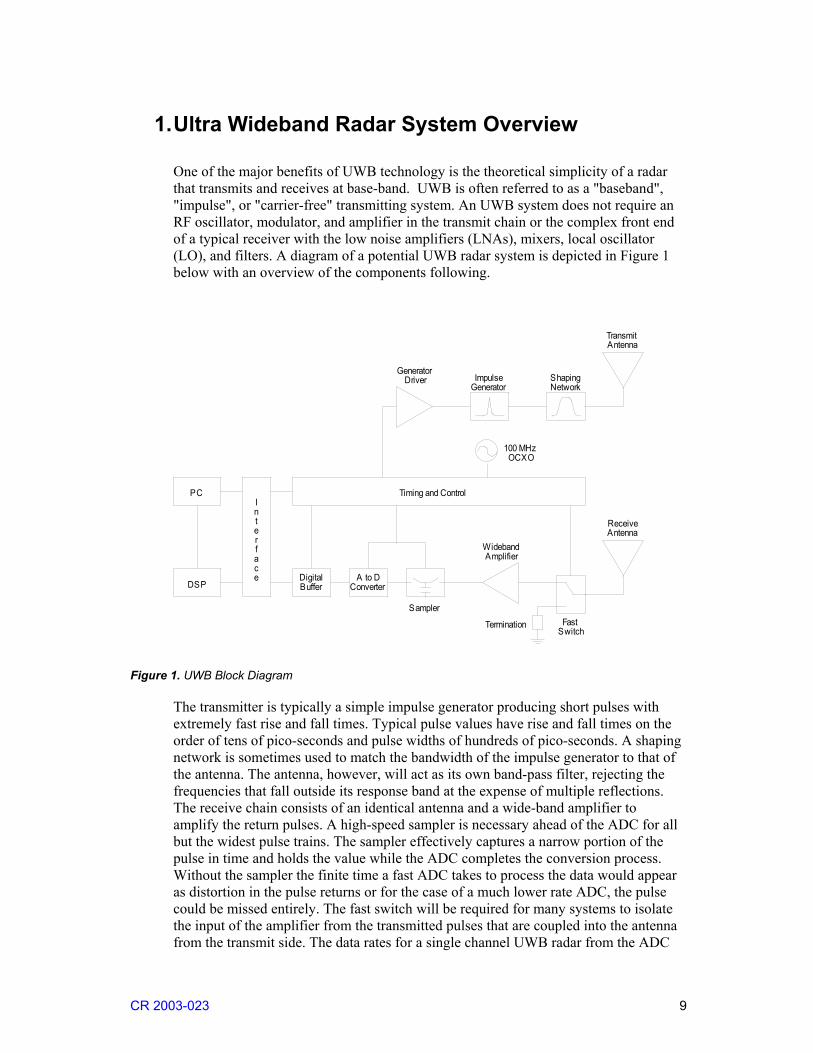
1. Ultra Wideband Radar System Overview
One of the major benefits of UWB technology is the theoretical simplicity of a radar that transmits and receives at base-band. UWB is often referred to as a "baseband", "impulse", or "carrier-free" transmitting system. An UWB system does not require an RF oscillator, modulator, and amplifier in the transmit chain or the complex front end of a typical receiver with the low noise amplifiers (LNAs), mixers, local oscillator (LO), and filters. A diagram of a potential UWB radar system is depicted in Figure 1 below with an overview of the components following.
Timing and Control
DigitalBuffer
A to DConverter
Interface
DSP
Sampler
PC
GeneratorDriver
Termination FastSwitch
ImpulseGenerator
ShapingNetwork
WidebandAmplifier
100 MHzOCXO
ReceiveAntenna
TransmitAntenna
Figure 1. UWB Block Diagram
The transmitter is typically a simple impulse generator producing short pulses with extremely fast rise and fall times. Typical pulse values have rise and fall times on the order of tens of pico-seconds and pulse widths of hundreds of pico-seconds. A shaping network is sometimes used to match the bandwidth of the impulse generator to that of the antenna. The antenna, however, will act as its own band-pass filter, rejecting the frequencies that fall outside its response band at the expense of multiple reflections. The receive chain consists of an identical antenna and a wide-band amplifier to amplify the return pulses. A high-speed sampler is necessary ahead of the ADC for all but the widest pulse trains. The sampler effectively captures a narrow portion of the pulse in time and holds the value while the ADC completes the conversion process. Without the sampler the finite time a fast ADC takes to process the data would appear as distortion in the pulse returns or for the case of a much lower rate ADC, the pulse could be missed entirely. The fast switch will be required for many systems to isolate the input of the amplifier from the transmitted pulses that are coupled into the antenna from the transmit side. The data rates for a single channel UWB radar from the ADC

will be as high as 20 GS/S, far too high for any current data bus to handle. The digital buffer can reduce the raw data rates from the ADC by integrating each frame of data gathered during the pulse repetition interval (PRI). This process is also necessary in order to increase the return signals amplitude above the noise floor. If for example we integrate 100 frames of data, the rate drops to a more manageable 200 MB/S, which can be transferred across the bus interface to the digital signal processor (DSP) for further processing. The personal computer (PC) acts as the high-level controller and display for the processed returns from the DSP. The various parameters such as PRI, integration number, processing algorithms and display modes would be set by the PC. The timing section controls all the parameters that must be closely coupled in order to keep the radar and any processing coherent. The timing for this type of system is critical, more so than most systems due to the short range of these types of radars. Short-term accuracy for the radar will need to be on the order of tens of pico-seconds for the system to be successful.
CR 2003-023 11
2. Time and Distance Requirements Ultra wideband radars use short pulses with fast rise & fall times to generate a broad RF frequency spectrum. Through the wall radar typically involves short distances compared with conventional systems designed to detect objects at much greater ranges. Two-way path times for a through-the-wall radar with a maximum range of 15 meters are illustrated in Figure 2. As can be seen from the illustration, the total measured round trip time for this hypothetical radar is just 100 nano-seconds. In order to have a resolution of one centimetre in distance, we need to measure accurately to less than 100 pico-seconds. This implies a stability of parts in 10-10 during the transmission and data acquisition time. For a coherent radar system a master oscillator controls all the system timing from the PRI to the timing of the ADCs. As the time duration for transmission and reception is extremely brief, short term stability and accuracy are the primary specifications of concern for system control. Compact rhubidium standards and crystal oscillators were both considered for the master oscillator as they offer a high degree of accuracy in a compact format. However, on closer examination of the two the oven controlled crystal oscillator offers better short-term stability and accuracy.
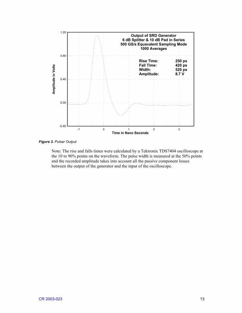
The impulses from this type of radar are less than one nano-second in duration with rise and fall times of tens to hundreds of pico-seconds. The pulse height ranges from several volts to hundreds and in some cases can be in the kilo-volt region. Typical radar evaluation test-beds of this type of system are designed to detect objects such as people at short standoff distances. The output of this radar’s pulse generator is shown in Figure 3. This type of output is typical of a step recovery diode which in all likely hood is the device used to generate the pulse.

0 1 2 3 4 5 6 7 8 9 10 11 12 13 14 15Distance in Meters
0
10
20
30
40
50
60
70
80
90
100
Tim
e in
Nan
o Se
cond
s
Two Way TimeUWB Radar
t=2d/c (s)
Figure 2. UWB Time to Distance
CR 2003-023 13
-1 0 1 2 3Time in Nano Seconds
-0.40
0.00
0.40
0.80
1.20
Am
plitu
de in
Vol
ts
Output of SRD Generator6 dB Splitter & 10 dB Pad in Series
500 GS/s Equavalent Sampling Mode1000 Averages
Rise Time: 250 psFall Time: 420 psWidth: 520 psAmplitude: 8.7 V
Figure 3. Pulsar Output
Note: The rise and falls times were calculated by a Tektronix TDS7404 oscilloscope at the 10 to 90% points on the waveform. The pulse width is measured at the 50% points and the recorded amplitude takes into account all the passive component losses between the output of the generator and the input of the oscilloscope.

3. Antenna Considerations Most conventional antennae are designed to operate over a narrow frequency range that can be easily achieved for most bands of interest. However, systems with a fractional bandwidth greater than twenty-five percent, as in UWB radar designs are extremely challenging to produce. The trade-offs of wide bandwidth, good match, and small size, while preserving the fidelity of the original signal is at best a compromise design. A number of antennae types and some of their characteristics are summarized below:
Table 1. Antennae Characteristics
TYPE BANDWIDTH POLARIZATION SIZE
Spiral Large Circular Small
Patch Small Linear/Circular Small
Slot Medium Linear Small
Log period Wide Linear Medium
Yagi Wide Linear Medium
TEM Wide Linear Large
Bow-Tie Wide Linear Small
The table footnote
This list is by no means complete, but included here to illustrate some of the more common designs and their limitations. In the case of an antenna with limited bandwidth and a poor impedance match an impulse at the input would lead to ringing at the output, severely distorting the shape of the pulse, spreading out the energy in time. In addition to the characteristics shown in the table above, dispersion is also a problem in pulse applications such as ours. This requirement eliminates log periodic and spiral antennas, as they are dispersive in nature and unsuitable for short pulse applications. Some antenna types such as the patch can have its bandwidth extended considerably by stacking multiple resonant sections of different dimensions to simulate a single wide-band element. However, this is done at the expense of greater complexity in the design, simulation, and construction of the device. A summary of desirable antenna characteristics for UWB applications is:
• Wide band-width • Good impedance match • Minimum waveform ringing • Minimize pulse dispersion • Wide beam-width (application dependent) • Small size • Low cost
The last two items on the list become important when one considers that any practical UWB radar system will ultimately need to be portable and will probably incorporate arrays of antennae in the design, hence the need for small size and lost cost in addition to the RF
CR 2003-023 15
requirements. For these reasons the bow-tie antenna configuration was chosen as the best compromise solution from both a technical point of view and to be able to complete a working system in the shortest possible time. Also note that for similar reasons, dual feed antennae designs such as dipoles were eliminated due to the complexity required to design and construct a matching balun or input network. Wideband baluns are not readily available for the frequency bands of interest for our radar system. Ground penetrating radar (GPR) applications use antennae with similar restrictions required by the through the wall system. There are three types of antennae used in GPR applications: the element antennas, the frequency independent antennas and the horn antennas. Examples of element antennas are the monopole, dipole, biconical dipole, and bowtie. They are non-dispersive, and characterized by linear polarization, low directivity and relatively limited bandwidth. A frequency independent antenna such as the spiral has circular polarization and radiates different frequency components from different parts of the antenna. This distorts and stretches out the radiated waveform, leading to dispersive behavior. The third type of antenna is the horn antenna. Classical horn antennas have a 3dB bandwidth of one octave (larger bandwidths are achieved with double-ridged horns) and are directive. Other antennas achieve good impulsive behavior at the cost of poor matching and large reflections. To combat this, still other antennas use resistive loading, which yields good matching and a high impedance bandwidth at the cost of lowered radiation efficiency.
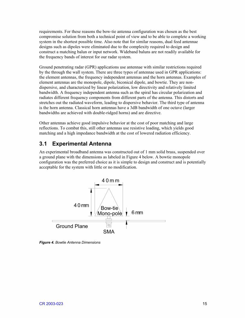
3.1 Experimental Antenna An experimental broadband antenna was constructed out of 1 mm solid brass, suspended over a ground plane with the dimensions as labeled in Figure 4 below. A bowtie monopole configuration was the preferred choice as it is simple to design and construct and is potentially acceptable for the system with little or no modification.
4 0 m m
Bow-tieMono-pole
SMAGround Plane
4 0 m m 6 m m
Figure 4. Bowtie Antenna Dimensions
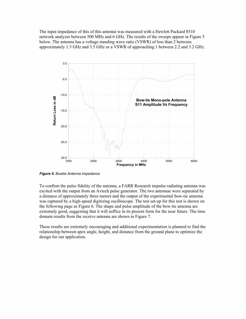
The input impedance of this of this antenna was measured with a Hewlett Packard 8510 network analyzer between 500 MHz and 6 GHz. The results of the sweeps appear in Figure 5 below. The antenna has a voltage standing wave ratio (VSWR) of less than 2 between approximately 1.5 GHz and 3.5 GHz or a VSWR of approaching 1 between 2.2 and 3.2 GHz.
1000 2000 3000 4000 5000 6000Frequency in MHz
-30.0
-25.0
-20.0
-15.0
-10.0
-5.0
0.0
Ret
urn
Loss
in d
B
Bow-tie Mono-pole AntennaS11 Amplitude Vs Frequency
Figure 5. Bowtie Antenna Impedance
To confirm the pulse fidelity of the antenna, a FARR Research impulse radiating antenna was excited with the output from an Avtech pulse generator. The two antennae were separated by a distance of approximately three meters and the output of the experimental bow-tie antenna was captured by a high-speed digitizing oscilloscope. The test set-up for this test is shown on the following page as Figure 6. The shape and pulse amplitude of the bow-tie antenna are extremely good, suggesting that it will suffice in its present form for the near future. The time domain results from the receive antenna are shown in Figure 7. These results are extremely encouraging and additional experimentation is planned to find the relationship between apex angle, height, and distance from the ground plane to optimize the design for our application.

CR 2003-023 17
TDS7404 OSCILLOSCOPE
MatchedCable Receive
ExperimentalBow-tie Antenna
P R F R A N G E ( H Z )
T R I G
AVTECH-3B-C
P O W E R
P R F
T T L I N T E X T
D E L A Y
A M P L I T U D E( 4 5 0 V O L T S M A X )
O U T5 0 O H M S
D E L A Y
A D V A N C E D E L A YMatchedCable
Splitter
MatchedCable
Transmit
FARR RESEARCH INC.IMPULSE ANTENNA
MODEL FRI-IRA-1
Figure 6: Antenna Test Set-up
-3 -2 -1 0 1 2 3 4 5 6 7Time in nS
-0.30
-0.20
-0.10
0.00
0.10
0.20
0.30
Am
plitu
de in
Vol
ts
Test Antenna Return
Figure 7: Antenna Time Domain Results

4. Impulse Generation For generating the extremely short pulses with their associated fast rise or fall times, it quickly became apparent that the only practical candidate device was the step recovery diode. These devices generate pulses with rise or fall times from tens to hundreds of pico-seconds. A step recovery diode is a pin junction diode that has a special doping profile, to give it an unusual characteristic curve. The idealised current characteristic of a step recovery diode is shown in Figure 8, along with the output spike produced by this rapidly changing current. Like a normal pn diode, the SRD conducts when forward biased, however, it also shows significant conduction when reversed biased. This only continues for a brief time, after which the diode snaps back to its non-conducting state. The transition time from the conducting to non-conducting states of the reversed biased diode occur in a time of typically less than 100 ps. Due to the extremely fast transition time, the current waveform has a high harmonic content and can be used for generating short pulses. Step recovery diodes are available as individual diodes, or as a module containing the SRD and a few passive components. SRD’s have three main applications:
1) As a multiplier, multiplying an input frequency by a fixed integer. E.g. a typical x7 multiplier module, driven at 1 GHz would produce an output at only 7 GHz.
2) Comb generators, these generate a number of harmonics simultaneously, which appears as a comb if viewed on a spectrum analyser.
3) SRDs are used to sharpen the rise and fall times as well as reduce the pulse widths generated by other components.
Figure 8. Step Recovery Diode Idealized Response
Due to the different conduction states of SRDs, the input and output impedance varies by a wide margin and requires a matching network designed for the correct PRF desired for the radar. An example of a typical network and its associated components appears in Figure 9 below. Typical specifications for a range of one brand of SRDs is also listed in Table 2.

CR 2003-023 19
Figure 9. Step Recovery Diode Matching Network
Table 2. Typical Step recovery Diode Specifications
JUNCTION CAPACITANCE
CARRIER LIFETIME TRANSITION TIME BREAKDOWN VOLTAGE
0.2 - 0.4 pf 8 nS 60 pS 15 V
0.4 – 0.6 pf 8 nS 60 pS 15 V
0.2 - 0.4 pf 11 nS 70 pS 20 V
0.4 - 0.6 pf 11 nS 70 pS 20 V
0.2 - 0.4 pf 17 nS 100 pS 30 V
0.4 - 0.6 pf 17 nS 100 pS 30 V
0.2 - 0.4 pf 21 nS 150 pS 40 V
0.4 - 0.6 pf 21 nS 150 pS 40 V
Partial list of MicroMetrics MSD 700 series step recovery diodes.
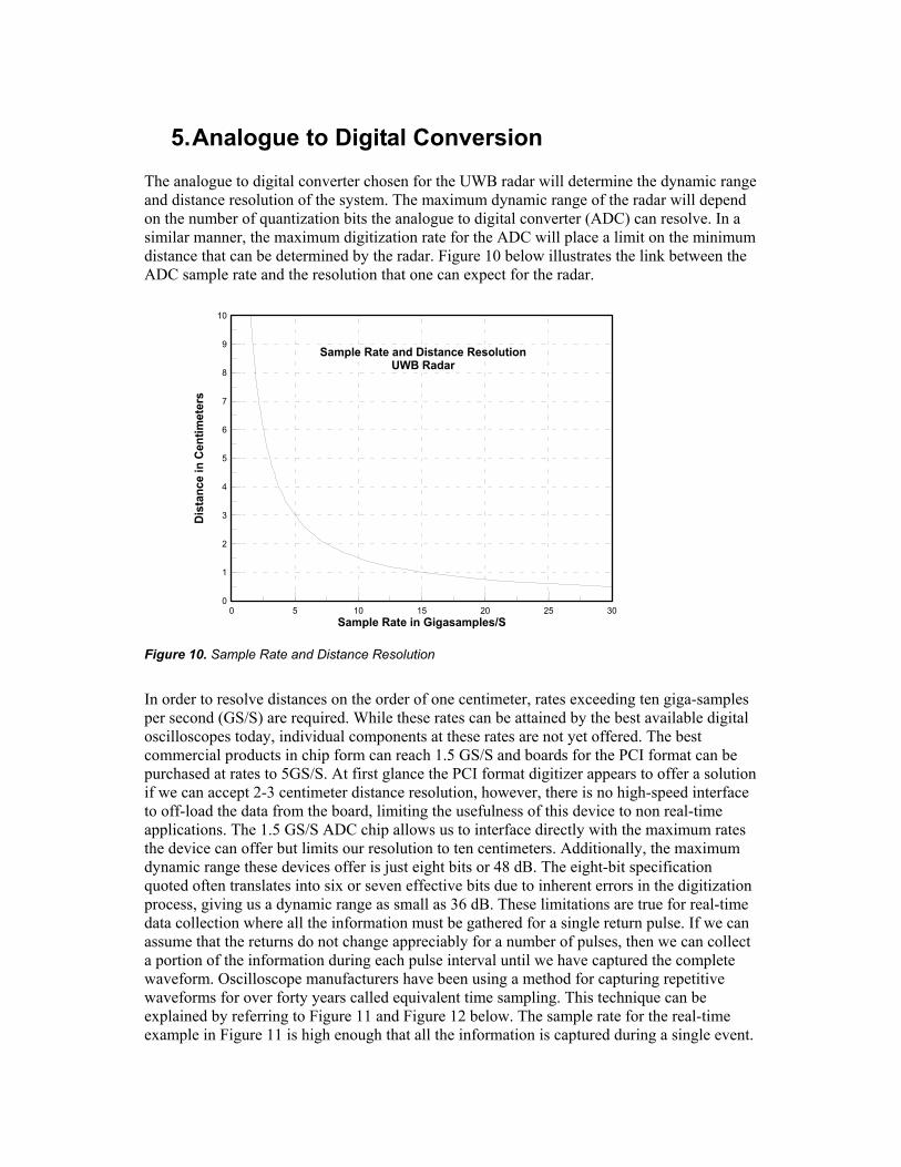
5. Analogue to Digital Conversion The analogue to digital converter chosen for the UWB radar will determine the dynamic range and distance resolution of the system. The maximum dynamic range of the radar will depend on the number of quantization bits the analogue to digital converter (ADC) can resolve. In a similar manner, the maximum digitization rate for the ADC will place a limit on the minimum distance that can be determined by the radar. Figure 10 below illustrates the link between the ADC sample rate and the resolution that one can expect for the radar.
0 5 10 15 20 25 30Sample Rate in Gigasamples/S
0
1
2
3
4
5
6
7
8
9
10
Dis
tanc
e in
Cen
timet
ers
Sample Rate and Distance ResolutionUWB Radar
Figure 10. Sample Rate and Distance Resolution
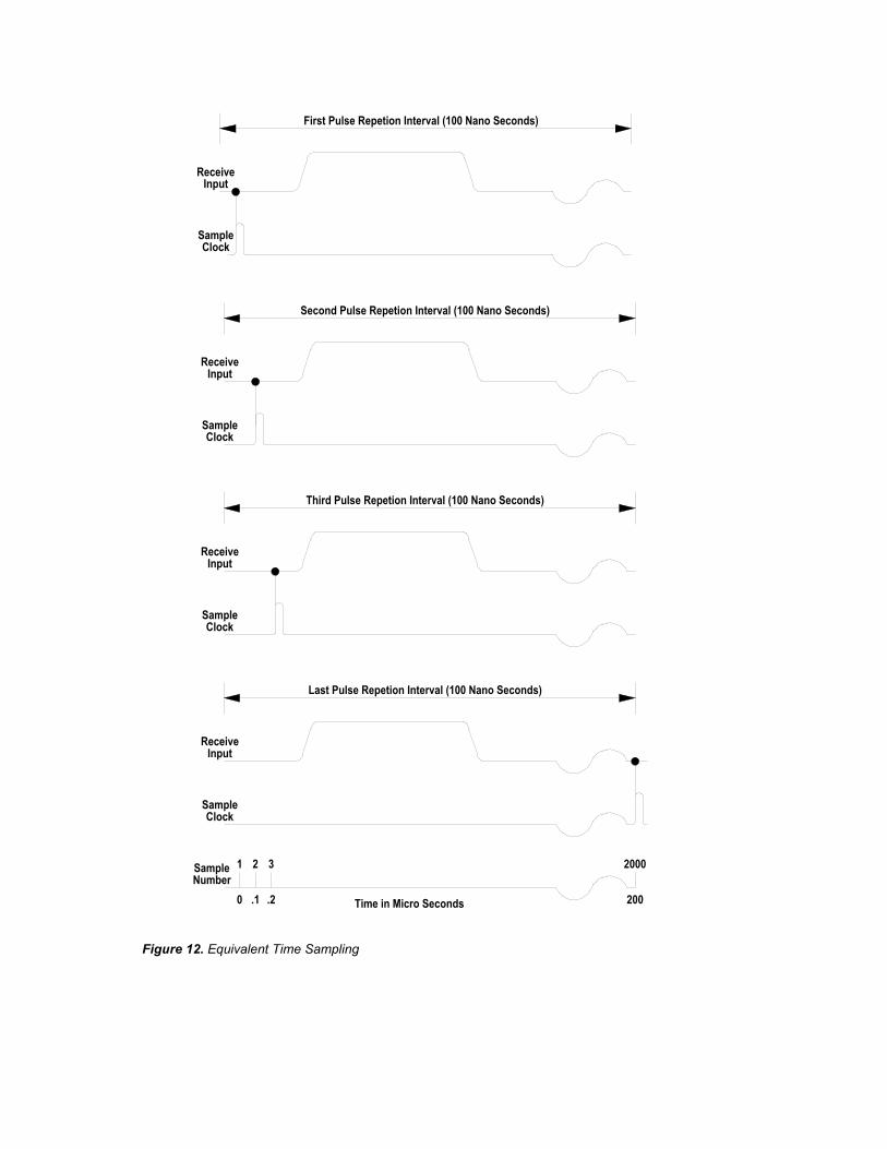
In order to resolve distances on the order of one centimeter, rates exceeding ten giga-samples per second (GS/S) are required. While these rates can be attained by the best available digital oscilloscopes today, individual components at these rates are not yet offered. The best commercial products in chip form can reach 1.5 GS/S and boards for the PCI format can be purchased at rates to 5GS/S. At first glance the PCI format digitizer appears to offer a solution if we can accept 2-3 centimeter distance resolution, however, there is no high-speed interface to off-load the data from the board, limiting the usefulness of this device to non real-time applications. The 1.5 GS/S ADC chip allows us to interface directly with the maximum rates the device can offer but limits our resolution to ten centimeters. Additionally, the maximum dynamic range these devices offer is just eight bits or 48 dB. The eight-bit specification quoted often translates into six or seven effective bits due to inherent errors in the digitization process, giving us a dynamic range as small as 36 dB. These limitations are true for real-time data collection where all the information must be gathered for a single return pulse. If we can assume that the returns do not change appreciably for a number of pulses, then we can collect a portion of the information during each pulse interval until we have captured the complete waveform. Oscilloscope manufacturers have been using a method for capturing repetitive waveforms for over forty years called equivalent time sampling. This technique can be explained by referring to Figure 11 and Figure 12 below. The sample rate for the real-time example in Figure 11 is high enough that all the information is captured during a single event.

CR 2003-023 21
In Figure 11 we are digitizing at a 20 giga-sample per second rate during a period of one hundred nano-seconds for a total of two thousand samples. The sample clock increments once every 50 pico-seconds until the entire waveform is captured. For the equivalent time case shown in Figure 12 the sample rate is much lower and the waveform is accumulated during the course of many PRIs. For each PRI a single sample point is acquired, each additional sample is acquired by delaying the measured point in the waveform to correspond to the next point in time as in the real-time case. The trade-off is the number of pulse repetition intervals (PRIs) that must elapse before we have acquired the complete waveform. The time scale for each sample in Figure 12 bears this out as each sample now requires a complete PRI or 100 nS. For our 100 nS acquisition range radar, the time for 2000 sample is 100 ns x 2000 or 200 micro-seconds as opposed to the real time case of 100 ns.
Time in Nano Seconds0.45
One Complete Pulse Repetion Interval (100 Nano Seconds)
87654321
0.100.05 0.15 0.20 0.25 0.30 0.35 0.40
SampleNumber
ReceiveInput
SampleClock
11 201918171615141312109
0.50 0.55 0.60 0.65 0.70 0.75 0.80 0.85 0.90 0.95 1.00
2000
100.00
Figure 11. Real Time Sampling
Last Pulse Repetion Interval (100 Nano Seconds)
Time in Micro Seconds
1 2 3
0 .1 .2
SampleNumber
SampleClock
ReceiveInput
Third Pulse Repetion Interval (100 Nano Seconds)
SampleClock
ReceiveInput
ReceiveInput
SampleClock
First Pulse Repetion Interval (100 Nano Seconds)
Second Pulse Repetion Interval (100 Nano Seconds)
ReceiveInput
SampleClock
2000
200
Figure 12. Equivalent Time Sampling

CR 2003-023 23
A practical system could be a hybrid of the real-time and equivalent-time techniques, taking more than one sample during each PRI and repeating the process to fill in the missing points until the waveform is complete. The type of ADC and its effective number of bits will determine the speed and resolution available for a working system. A trade-off between the number of bits and sample rates available for different commercial ADCs and their technology is tabled below.
Table 3. Converter Technologies
CONVERTER TYPE NUMBER OF BITS SPEED SIZE & POWER
Delta Sigma 15 to 24 10 KS/S to 2 MS/S Small
Pipelined Up to 16 Up to 10 MS/S Moderate
SAR Up to 18 1MS/S to 10 MS/S Moderate
Flash 8 to 14 10 MS/S to 1.5 GS/S Moderate to High
A typical radar test bed may have a PRF of 1 to 10 MHz and an ADC resolution of eight to ten bits, depending on the sample rate. At the highest PRF with a 50 ps step size the radar requires 2000 pulses and 100 ns before a complete waveform is acquired for a range of 15 meters. The best dynamic range for this system at ten bit resolution is theoretically 60 dB. As a rule of thumb the greater the number of bits of resolution offered by the ADC, the slower the sample rate. The present technology points to either a 12 or 14 bit flash ADC as the best compromise between speed, power, size and resolution. A readily available 12 bit ADC from Analog Devices samples at 100 MS/S with 200 and 400 MS/S versions due in the next few months. They will also offer a 14 bit version that samples at 100 MS/S but with a larger footprint and greater power consumption that will be an issue for a portable system with multiple receive channels. A hybrid sampling system in this case would digitize the waveform at a constant 100 MHz rate during each PRI. For a 50 pS step, 10 samples would be acquired for each pulse transmitted. The next sample period would be delayed by 50 pS as in the equivalent time method and another 10 samples would be acquired. For the 15 meter radar example the number of PRIs required to collect a complete waveform would be reduced by a factor of ten. In addition, the dynamic range for the 12 bit ADC is theoretically 72 dB, a considerable improvement over any potential real time ADC. This hybrid combination of these two common technologies is illustrated for a system in Figure 13. The total time to collect the data would be 200 x 100ns or 20 micro-seconds.

Second Pulse Repetion Interval (100 Nano Seconds)
Last (200th) Pulse Repetion Interval (100 Nano Seconds)
Third Pulse Repetion Interval (100 Nano Seconds)
First Pulse Repetion Interval (100 Nano Seconds)
Total Waveform Acquisition Time in Micro Seconds
ReceiveInput
SampleNumber
SampleClock
SampleTaken
Time in Nano Seconds
2010 30
0.10 0.20 0.30
SampleNumber
SampleClock
ReceiveInput
SampleClock
ReceiveInput
SampleNumber
SampleClock
ReceiveInput
SampleNumber
Time in Nano Seconds
Time in Nano Seconds
21
0.10
0.05
11
Time in Nano Seconds
1
0.00
Points 1991-2000
Each Point has +9.95 nS offest50 6020 30 40100 70 80 90
2000
200
Each Point has +0.05 nS offest
Each Point has +0.10 nS offest50
26
50
16
20 30 4010
22 23 24 25
20 30 4010
12 13 14 15
70
28
60
27
80 90
29 30
70
18
60
17
80 90
19 20
50
62
10 20 30 40
3 4 5 10
60 70 80 90
7 8 9
Figure 13. Hybrid Sampling System

CR 2003-023 25
6. Sampling Network and Timing
Perhaps the greatest challenge is the high-speed sampler and system timing precision that will be required to preserve the fidelity of the return pulse waveforms. The aperture of the sampler will need to be on the order of tens of picoseconds for the sample rates suggested in the previous section, whether equivalent or real-time. In effect the aperture size puts a limit on the minimum detail of the return waveforms we can observe. The system timing accuracy coupled with the aperture size dictates the maximum sample rate obtainable for the system. In addition to the timing accuracy we will have jitter on the signal that will translate into distortion of the waveform. Typical jitter values are on the order of a few picoseconds are not uncommon, one manufacturer quotes a minimum step size of 15 pico-seconds which is probably a combination of jitter and device limitations. The only source found for a commercial sampler with these specifications is from a company called Picosecond™. This company specializes in pulse generation with extremely fast rise and fall times (to 3 ps) and associated support hardware. They produce a 100 GHz sampler that will be available later this year with an aperture width of 3 picoseconds. In the meantime a substitute will be required as no other source has been found as yet. An interesting idea would be to use an RF mixer as the front end sampling network as they effectively operate in this mode for down-converting an RF signal to base-band. If we drive the input of the LO with an SRD acting as the source, we are sampling the pulsed RF input with an aperture fixed by the pulse width of the SRD, which can be on the order of tens of picoseconds.
Figure 14. Typical Mixer Schematic

The timing required to place the aperture at the correct instant in time for the equivalent sampling technique described may also have a novel solution as this technology is not readily available from the manufacturers of this equipment. An innovative approach involves the use of a clock de-skewing product for the telecom sector to align high-speed data streams at gigahertz rates. A new product from ON Semiconductor™ has the virtue of a ten nano-second maximum delay that can be programmed with a ten bit digital word that translates into a minimum step size of 10 pico-seconds. The ten nano-second delay time aligns perfectly with the 100 MHz clock frequency proposed for the master oscillator timing for the system. The 10 nano-second period would be further divided into 100 equal time steps of 100 ps to give us a sample rate of 10 GS/s. The step sizes required by the delay generator for the digitizer fall well within the capabilities of the MC100EP196 chip shown below in Figure 15.
D10
LEN
SET MAX
SET MIN
LATCH
CASCADE
CASCADE
D1D0
IN
IN
EN1
GD 1
0
1
0
2GD
D2 D3
10 BIT LATCH
D4
1
0
4GD
8GD 1
0
32GD1
0
16GD
D5 D6 D8D7
128GD1
0
1
0
64GD 1
0
256GD 1
0
D9
1
0
FTUNE0-60psDelay
1GD1
0
512GD
Q
Q
Figure 15. MC100EP196FA
The MC100E196 uses the inherent delays of a basic logic gate as a fundamental unit of time. By combining a number of gates together, fixed delays of known values can be produced. For this device ten blocks of varying numbers of gates are placed together in series, with each successive delay double the value of the previous one. At each fixed delay a switch allows for incorporating or bypassing each block. In this manner, any delay between the minimum value of 10 ps and the maximum of 10 ns can be obtained. In addition to the 10 ps discrete steps available to the user there is a fine tune line (FTUNE) input that can be used to introduce a variable 0-60 ps delay for adjusting the output to better than 1 ps accuracy. Figure 16 on the next page gives a more detailed view of the last few digital delay taps and the analogue fine tune line. Some of the functionality of the device has been left out for clarity, however, the basic operation is accurately depicted. The last two digital sections show 256 and 512 gate delays respectively, with the bypass switches and the analogue fine tune line. The outputs are available inverted as well as non-inverted.

CR 2003-023 27
Digital Gate Delays
256GD
D8
1
From Previous Delay
D0-D7 Gate Delays
0 Q
D9
1512GD
0-60psDelay
FTUNE
0
Analogue Delay
Q
Figure 16. MC100EP196FA Detail View
The key to using this device in this role is to calibrate the 100 ps steps precisely before driving the sampler gates. For this application, either a state machine or a microprocessor can be used to calibrate out the errors by measuring a known stable source. With a known waveform, the exact errors introduced by the inaccuracies of the device can be ascertained and calibrated out. The ideal candidate would be the 100 MHz master oscillator via a simple RF switch at the input of the delay generator. The master oscillator would be digitized by the system in the usual manner and the results used to create a look-up table for the DAC that would fine-tune the output to correspond to the correct delays at each step.
10 BitDigital Delay
RF ReturnSample
100 MHzClock
To Sampler
Switch
SampleTrigger
DigitalSamples
Input
MCU
D to A
60 pSFine Tune
Delayed Trigger
Figure 17. Calibrated Programmable Delay
Figure 17 on the previous page shows a block diagram of the system with the components required to calibrate the delay line. The sampler would digitize the reference waveform and use the results to create a look-up table to correct the delay

inaccuracies. This table of corrected values would be passed to the microprocessor and used as each delay step is incremented to ensure the sampler is positioned accurately in time for the digitizer. At this point the RF switch would change position to capture the RF returns.
10 ClockGate
100 MHzOXCO
/100
1 MHzPRI
To DelayGenerator
To SRDGenerator
To DelayCalibration
Figure 18. Basic System Timing
With the system calibrated the 100 MHz oscillator signal would be distributed as shown in Figure 18 above. Dividing the reference frequency by a factor of one hundred will produce the 1 us time interval to derive the PRI. This is the signal used to drive the SRD for the output pulse waveform. The oscillator would then be gated by the PRI to produce the ten-sample burst collected during each pulse. It is this signal that would be delayed during each subsequent burst by the delay generator to collect the rest of the samples to complete the entire waveform, one-hundred PRIs later. Lastly, as noted before, the reference oscillator would also be made available to the digitizer through an RF switch for calibration purposes.

CR 2003-023 29
7. Discussion Each of the areas of concern has been investigated and potential solutions proposed in order to complete a laboratory test bed for UWB radar. The next logical step is to build a prototype for each of the sub-systems and solve any practical engineering issues that arise in the implementation. Each of these systems will need to be characterized and the results analyzed to ensure that the minimum specifications required can be met. The major system components to be constructed and tested are:
• Antenna: Although the S11 sweep with the network analyzer looks promising, the pulse fidelity in time will need to be determined. The simplest method would be to mount two of these antennae across the room from each other and measure the difference between the transmitted pulse at the antenna input and the return pulse from the receive antenna output. With a good understanding of the limitations of the initial design, we should explore variations of the monopole by changing the apex angle, height above the ground plane, and the two major dimensions to derive an empirical formula for the bandwidth and center frequency. The possibility of micro-strip antennae should also be considered for this application, perhaps using a variation of the proposed design as both a monopole and dipole.
• Impulse Generation: A step recovery diode impulse generator will need to be
constructed and the rise, fall, and pulse widths measured to see if they meet the minimum specifications required for the design. The amplitude of the pulse will also be an issue, as it will determine the peak power of the radar. Application notes on the design of SRDs for pulse generators are readily available by many manufacturers of the devices, so this should be a straight forward engineering design exercise. However, if it is found that much higher output levels are required, then a different approach will need to be investigated.
• Analogue to Digital Conversion: This is one area where there is little risk with
the proposed design as a major supplier of these devices can furnish the product mounted on an evaluation board complete with software to test the chip. In particular, the software allows one to capture an analogue signal at the maximum conversion rate of the device and save the results to a personal computer for further assessment. Using this approach we can test the timing and sampler designs once they have been completed and compare the results with the minimum specifications required for the radar.
• Sampler: As we are using a mixer for the sampler it will need to characterized
for this application as the purpose deviates from its original function. In this application we would drive the RF input in the usual manner with the return pulse. The local oscillator port will be driven with the extremely short duration pulses generated by a SRD pulse generator. The sampled output will be taken from the intermediate port and digitized by the A to D converter. A re-constructed signal would be compared with the original for any deviation.
• System Timing: This is by far the most crucial component of the entire system as it has a direct bearing on the signal fidelity and accuracy of the received waveforms. The delay generator will be calibrated as noted in the timing section

of this paper and the delay step will be incremented in real time during the measurements. Any settling time or deviation from the expected delay will be noted and corrective action taken, if necessary. One of the areas of concern for this device is the temperature stability with time. It may be necessary to ovenize the entire timing sub-system in order top maintain the tight timing requirements during the course of a measurement set.
Once the individual components of the system have been tested and a sound design for each frozen, the glue logic to interface these parts will need to be undertaken. The most likely candidate for this would be a field programmable gate array (FPGA). The logical control device for the initial laboratory system would be a PC fro ease of use and display purposes.

CR 2003-023 31
References
1. The Use of the Genetic Algorithm Approach in the Design of Ultra-wideband Antennas, Aaron Kerkhoff & Robert Rogers (Applied Research Laboratories, University of Texas – Austin), Hao Ling, (Department of Electrical and Computer Engineering, University of Texas – Austin)
2. Impedance Characteristics of Trapezoidal Planer Monopole Antennas, Zhi Ning Chen1 and Y. W. M. Chia1, Centre for Wireless Communications, Singapore 117674
3. New Considerations in the Design of Microstrip Antennas, Naftali Herscovici, Senior Member, IEEE
4. A Wide-Band Single-Layer Patch Antenna, Naftali Herscovici, Senior Member, IEEE
5. Design of a Dual Patch Triangular Microstrip Antenna, By S. H. Al-Charchafchi, W .K. Wan Ali, M. R. Ibrahim and S. R. Barnes, Cranfield College of Aeronautics, Cranfield University
6. MicroMetrics MSD 700 Series Data Sheet
7. Hewlett Packard Application Note 918, Pulse and Waveform Generation with Step Recovery Diodes. November 1984.
8. Analog-to-Digital Converter Architectures and Choices for System Design, By Brian Black of Analog Devices
9. Sampling Oscilloscope Techniques, Tektronix Technique Primer 47W-7209
10. ON Semiconductor MC100EP196 Data Sheet
11. ON-Display, Third Quarter 2002, Volume 2, Number 2.
List of symbols/abbreviations/acronyms/initialisms
DND Department of National Defence
UWB Ultra Wide Band
LNA Low Noise Amplifier
LO Local Oscillator
VSWR Voltage Standing Wave Ratio
SRD Step recovery Diode
GS/S Giga Samples per Second
ADC Analogue to Digital Converter
PRI Pulse Repetition Interval
PRF Pulse Repetition Frequency
DSP Digital Signal Processor
GPR Ground Penetrating Radar
FPGA Field Programmable Gate Array

CR 2003-023 33
Glossary
Technical term Explanation of term
Micro 1 x 10⁻⁶
Nano 1 x 10⁻⁹
Pico 1 x 10-12
Giga 1 x 10+9
SMA RF Connector
FTUNE Fine Tune Control for Digital Delay Generator
PCI Bus 64 Bit Peripheral Component Interconnect Bus Standard
Picosecond™ Company specializing in high speed time domain
ON Semi™ Company specializing in advanced ECL logic

UNCLASSIFIED SECURITY CLASSIFICATION OF FORM
(highest classification of Title, Abstract, Keywords)
DOCUMENT CONTROL DATA (Security classification of title, body of abstract and indexing annotation must be entered when the overall document is classified)
1. ORIGINATOR (the name and address of the organization preparing the document. Organizations for whom the document was prepared, e.g. Establishment sponsoring a contractor’s report, or tasking agency, are entered in section 8.)
RWR Consulting
2. SECURITY CLASSIFICATION (overall security classification of the document,
including special warning terms if applicable) UNCLASSIFIED
3. TITLE (the complete document title as indicated on the title page. Its classification should be indicated by the appropriate abbreviation (S,C or U) in parentheses after the title.)
Through the Wall Ultra Wideband Radar: An Investigation into the Feasibility of Building an In-House UWB Radar Hardware Capability
4. AUTHORS (Last name, first name, middle initial)
Robinson Robert
5. DATE OF PUBLICATION (month and year of publication of document)
March 2003
6a. NO. OF PAGES (total containing information. Include Annexes, Appendices, etc.)
47
6b. NO. OF REFS (total cited in document)
11
7. DESCRIPTIVE NOTES (the category of the document, e.g. technical report, technical note or memorandum. If appropriate, enter the type of report, e.g. interim, progress, summary, annual or final. Give the inclusive dates when a specific reporting period is covered.)
Contract Report
8. SPONSORING ACTIVITY (the name of the department project office or laboratory sponsoring the research and development. Include the address.)
DRDC Ottawa
9a. PROJECT OR GRANT NO. (if appropriate, the applicable research and development project or grant number under which the document was written. Please specify whether project or grant)
12kc15
9b. CONTRACT NO. (if appropriate, the applicable number under which the document was written)
W7714 EN537-8-4015/001ZJ
10a. ORIGINATOR’S DOCUMENT NUMBER (the official document number by which the document is identified by the originating activity. This number must be unique to this document.)
10b. OTHER DOCUMENT NOS. (Any other numbers which may be assigned this document either by the originator or by the sponsor)
DRDC Ottawa CR 2003-023
11. DOCUMENT AVAILABILITY (any limitations on further dissemination of the document, other than those imposed by security classification) ( x ) Unlimited distribution ( ) Distribution limited to defence departments and defence contractors; further distribution only as approved ( ) Distribution limited to defence departments and Canadian defence contractors; further distribution only as approved ( ) Distribution limited to government departments and agencies; further distribution only as approved ( ) Distribution limited to defence departments; further distribution only as approved ( ) Other (please specify):
12. DOCUMENT ANNOUNCEMENT (any limitation to the bibliographic announcement of this document. This will normally correspond to
the Document Availability (11). However, where further distribution (beyond the audience specified in 11) is possible, a wider announcement audience may be selected.)
Unlimited
UNCLASSIFIED
SECURITY CLASSIFICATION OF FORM DDCCDD0033 22//0066//8877

UNCLASSIFIED SECURITY CLASSIFICATION OF FORM
13. ABSTRACT ( a brief and factual summary of the document. It may also appear elsewhere in the body of the document itself. It is highly desirable that the abstract of classified documents be unclassified. Each paragraph of the abstract shall begin with an indication of the security classification of the information in the paragraph (unless the document itself is unclassified) represented as (S), (C), or (U). It is not necessary to include here abstracts in both official languages unless the text is bilingual).
An investigation into the feasibility of producing in-house ultra wideband (UWB) radar for experimental purposes was undertaken. The principal purpose for this system will be for through the wall radar imaging. Several architectures were examined and the most promising avenues were explored further. Wherever possible off-the-shelf components were selected to shorten the development time and costs associated with a new technology such as UWB radar. For each challenging area a potential solution is put forward and a complete system could be produced for the single transmit and receive case by the end of this year. The solutions proposed lend themselves to a modular approach and could be scaled-up to produce a multiple transmit and receive radar system with little difficulty..
14. KEYWORDS, DESCRIPTORS or IDENTIFIERS (technically meaningful terms or short phrases that characterize a document and could be helpful in cataloguing the document. They should be selected so that no security classification is required. Identifiers such as equipment model designation, trade name, military project code name, geographic location may also be included. If possible keywords should be selected from a published thesaurus. e.g. Thesaurus of Engineering and Scientific Terms (TEST) and that thesaurus-identified. If it is not possible to select indexing terms which are Unclassified, the classification of each should be indicated as with the title.)
Ultra-wideband (UWB) Short-pulse (SP) Radars Through the wall surveillance
UNCLASSIFIED
SECURITY CLASSIFICATION OF FORM
