tiduc98a | ti.com - semiconductor company | ti.com
TRANSCRIPT
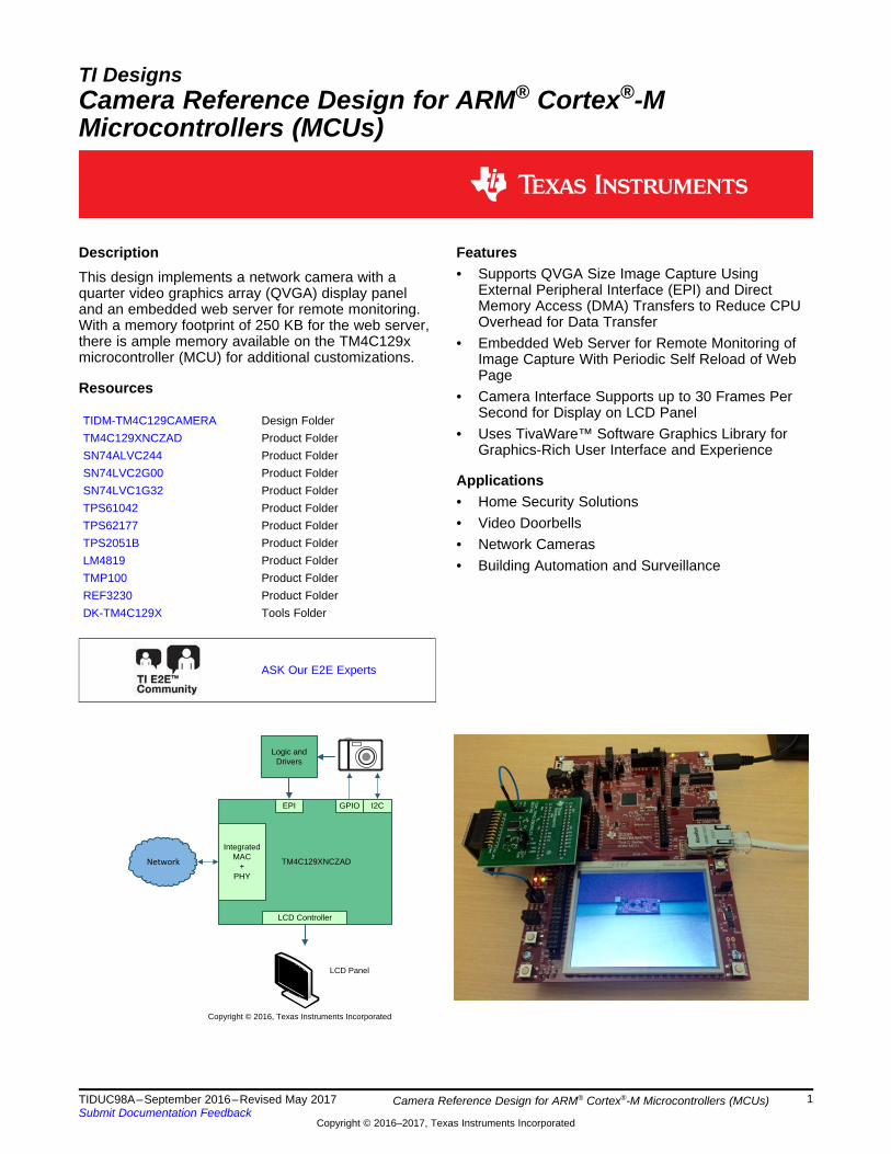
TM4C129XNCZAD
LCD Controller
IntegratedMAC
+PHY
EPI GPIO I2C
xx xLCD Panel
Logic and Drivers
Network
Copyright © 2016, Texas Instruments Incorporated
1TIDUC98A–September 2016–Revised May 2017Submit Documentation Feedback
Copyright © 2016–2017, Texas Instruments Incorporated
Camera Reference Design for ARM® Cortex®-M Microcontrollers (MCUs)
TI DesignsCamera Reference Design for ARM® Cortex®-MMicrocontrollers (MCUs)
DescriptionThis design implements a network camera with aquarter video graphics array (QVGA) display paneland an embedded web server for remote monitoring.With a memory footprint of 250 KB for the web server,there is ample memory available on the TM4C129xmicrocontroller (MCU) for additional customizations.
Resources
TIDM-TM4C129CAMERA Design FolderTM4C129XNCZAD Product FolderSN74ALVC244 Product FolderSN74LVC2G00 Product FolderSN74LVC1G32 Product FolderTPS61042 Product FolderTPS62177 Product FolderTPS2051B Product FolderLM4819 Product FolderTMP100 Product FolderREF3230 Product FolderDK-TM4C129X Tools Folder
ASK Our E2E Experts
Features• Supports QVGA Size Image Capture Using
External Peripheral Interface (EPI) and DirectMemory Access (DMA) Transfers to Reduce CPUOverhead for Data Transfer
• Embedded Web Server for Remote Monitoring ofImage Capture With Periodic Self Reload of WebPage
• Camera Interface Supports up to 30 Frames PerSecond for Display on LCD Panel
• Uses TivaWare™ Software Graphics Library forGraphics-Rich User Interface and Experience
Applications• Home Security Solutions• Video Doorbells• Network Cameras• Building Automation and Surveillance
TM4C129XNCZAD
LCD Controller
IntegratedMAC
+PHY
EPI GPIO I2C
xx xLCD Panel
Logic and Drivers
Network
Copyright © 2016, Texas Instruments Incorporated
System Description www.ti.com
2 TIDUC98A–September 2016–Revised May 2017Submit Documentation Feedback
Copyright © 2016–2017, Texas Instruments Incorporated
Camera Reference Design for ARM® Cortex®-M Microcontrollers (MCUs)
An IMPORTANT NOTICE at the end of this TI reference design addresses authorized use, intellectual property matters and otherimportant disclaimers and information.
1 System DescriptionThe TM4C129x family of MCUs from Texas Instruments feature an integrated Ethernet PHY and MACwith cryptographic modules and a large number of serial and parallel interfaces for control and sensordata acquisition. Integrating a camera would require a dedicated camera interface or an externalprogrammable logic like field programmable gate array (FPGA) and complex programmable logic device(CPLD) to interface a MCU to the camera. This design uses the EPI peripheral with a logic gate forprotocol conversion without needing an external FPGA or CPLD. Using EPI with the logic gate significantlyreduces the complexity of interfacing the camera to the TM4C129x device family while providing theadvantage of integrated PHY that allows network connectivity for a host of video monitoring applications.The design files include schematics, bill of materials (BOM), layer plot, Altium files, Gerber files, andembedded firmware.
1.1 Key System Specifications
Table 1. Key System Specifications
PARAMETER SPECIFICATIONImage capture width 320 pixelsImage capture depth 240 pixelsImage capture format 16 BPP (RGB565 format)
Raw camera clock 20 MHzDisplay panel width 320 pixelsDisplay panel depth 240 pixels
Image frame rate 30 frames per second
2 System Overview
2.1 Block Diagram
Figure 1. Camera Reference Design With TM4C129x Block Diagram
JTAG/SWDARM®
Cortex®-M4F
(120 MHz)
ETM FPU
NVIC MPU
System Control and Clock
(w/ Precis. Osc.)
TM4C129XNCZAD
DCode bus
ICode bus
ROM
Flash(1024 KB)
Boot LoaderDriverLibAES & CRCEthernet Boot Loader
Bus Matrix
System Bus
SRAM(256 KB)
SYSTEM PERIPHERALS
DMA
EEPROM(6 K)
GPIOs(140)
CRCModule
DESModule
TFT LCDController
Watchdog Timer
(2 Units)
General Purpose Timer
(8 Units)
External PeripheralInterface
AES Module
SHA/MD5Module
Hibernation Module
Temper
SERIAL PERIPHERALS
UART(8 Units)
USB OTG(FS PHY or ULPI)
SSI(4 Units)
EthernetMAC/PHY/MII
PWM(1 Units/8 Signals)
ANALOG PERIPHERALS
MOTHION CONTROL PERIPHERALS
SMC PERIPHERALS
I2c(10 Units)
CANController(2 Units)
12-Bit ADC(2 Units/ 24 Channels)
QEI(1 Unit)
1-Wire(1 Unit)
Analog Comparator(3 Units)
Copyright © 2017, Texas Instruments Incorporated
www.ti.com System Overview
3TIDUC98A–September 2016–Revised May 2017Submit Documentation Feedback
Copyright © 2016–2017, Texas Instruments Incorporated
Camera Reference Design for ARM® Cortex®-M Microcontrollers (MCUs)
2.2 Highlighted Products
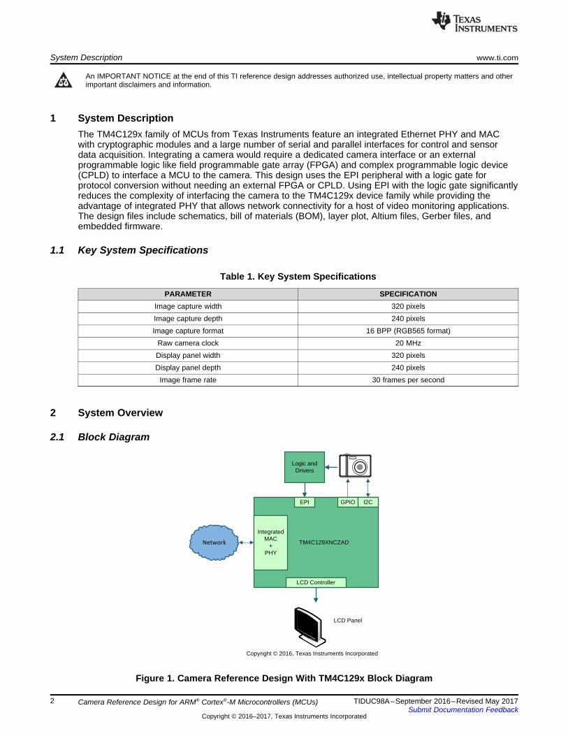
2.2.1 TM4C129XNCZADTM4C129XNCZAD is a 120-MHz high-performance MCU with 1-MB on-chip flash, 256-KB on-chip SRAMintegrated Ethernet MAC PHY for connected applications and cryptographic modules such as advancedencryption standard (AES), data encryption standard (DES) and secure hash algorithm (SHA) forencryption, decryption, data validation, and authentication. The device has high-bandwidth interfaces like amemory controller (EPI) and a high-speed USB 2.0 digital interface. With integration of a number of serialcommunication peripherals, a 12-bit analog-to-digital converter (ADC) capable of up to 4 MSPS andmotion control peripherals. The device provides a unique solution for a variety of applications ranging fromindustrial communication equipment to smart energy and smart grid applications.
Figure 2. TM4C129XNCZAD MCU High-Level Block Diagram
2.2.2 SN74ALVC244The SN74ALVC244 is organized as two four-bit line drivers with separate output-enable (OEn) inputs.When OEn is low, the device passes data from the A inputs to the Y outputs. When OEn is high, theoutputs are in the high-impedance state. This device provides extremely low-propagation delay of 2.8 ns(maximum) when operating at 3.3 V.
G3
G4
G5
R0
R1
R2
R3
R4
B0
B1
B2
B3
B4
G0
G1
G2
PixelClock
HREF
DATA
Pixel-0row data
Pixel-319
System Design Theory www.ti.com
4 TIDUC98A–September 2016–Revised May 2017Submit Documentation Feedback
Copyright © 2016–2017, Texas Instruments Incorporated
Camera Reference Design for ARM® Cortex®-M Microcontrollers (MCUs)
2.2.3 SN74LVC2G00The SN74LVCG200 is a dual two-input positive NAND gate designed for low-propagation delay over awide supply range of 1.65 to 5 V.
3 System Design TheoryThis section will elaborate how the TM4C129x MCU is interfaced to the external camera module using theEPI module.
3.1 Camera Module InterfaceThe camera module interface used for this reference design is the OV9655; however, other cameramodules with similar data, configuration, and control interfaces may be used.
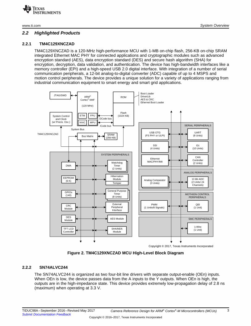
3.1.1 Camera Data InterfaceThe OV9655 has an eight-bit data interface, two additional control signals, and a pixel clock that areprovided by the camera. The data and the control signals are timing referenced with respect to the pixelclock. The camera provides the following signals.1. Pixel clock output2. Vertical sync output to indicate end of the frame3. Horizontal reference output to indicate valid data for pixels in a row4. Eight-bit data output
The following images illustrate the data sent by the camera module for every line (see Figure 3) for a 16-BPP QVGA resolution image. The camera data and HREF signal are launched on the falling edge of thepixel clock. The data is valid on every rising edge for sampling by the MCU only when the HREF is logichigh. Pixel position R4 and G2 correspond to MSB and pixel position G3 and B0 correspond to LSB.
Figure 3. Line Information From Camera
VSYNC
HREF
Row-0 Row-1 Row-238 Row-239
www.ti.com System Design Theory
5TIDUC98A–September 2016–Revised May 2017Submit Documentation Feedback
Copyright © 2016–2017, Texas Instruments Incorporated
Camera Reference Design for ARM® Cortex®-M Microcontrollers (MCUs)
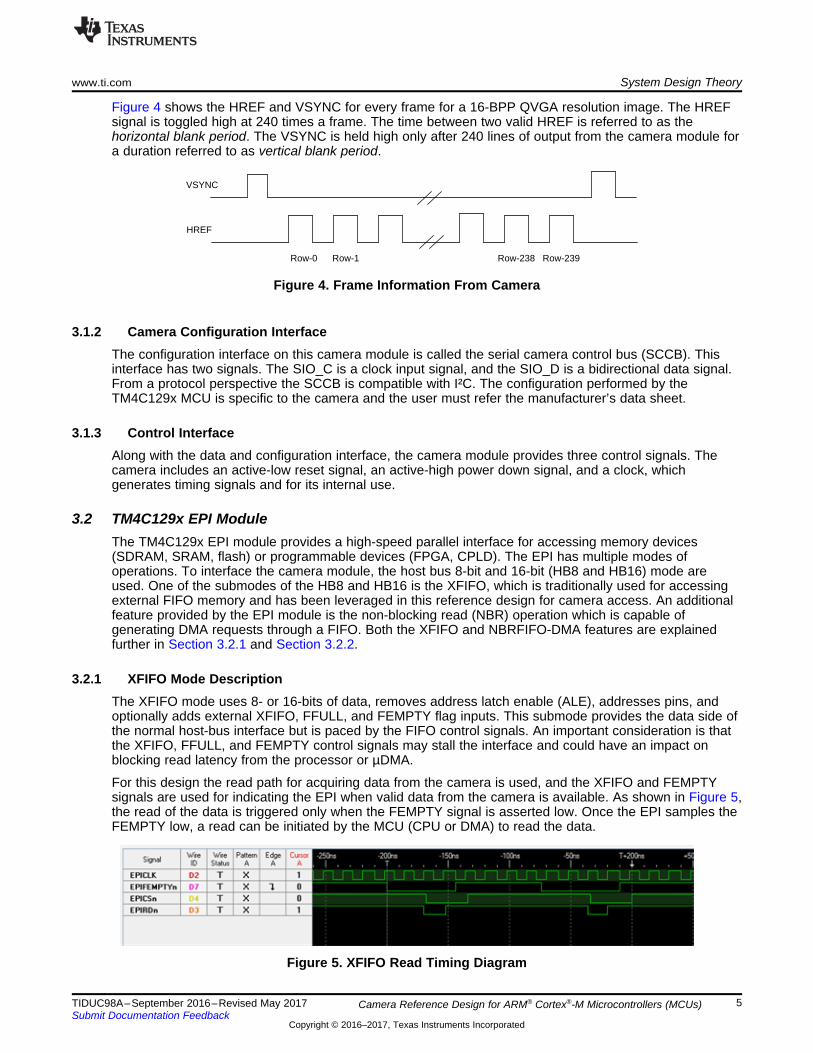
Figure 4 shows the HREF and VSYNC for every frame for a 16-BPP QVGA resolution image. The HREFsignal is toggled high at 240 times a frame. The time between two valid HREF is referred to as thehorizontal blank period. The VSYNC is held high only after 240 lines of output from the camera module fora duration referred to as vertical blank period.
Figure 4. Frame Information From Camera
3.1.2 Camera Configuration InterfaceThe configuration interface on this camera module is called the serial camera control bus (SCCB). Thisinterface has two signals. The SIO_C is a clock input signal, and the SIO_D is a bidirectional data signal.From a protocol perspective the SCCB is compatible with I²C. The configuration performed by theTM4C129x MCU is specific to the camera and the user must refer the manufacturer’s data sheet.
3.1.3 Control InterfaceAlong with the data and configuration interface, the camera module provides three control signals. Thecamera includes an active-low reset signal, an active-high power down signal, and a clock, whichgenerates timing signals and for its internal use.
3.2 TM4C129x EPI ModuleThe TM4C129x EPI module provides a high-speed parallel interface for accessing memory devices(SDRAM, SRAM, flash) or programmable devices (FPGA, CPLD). The EPI has multiple modes ofoperations. To interface the camera module, the host bus 8-bit and 16-bit (HB8 and HB16) mode areused. One of the submodes of the HB8 and HB16 is the XFIFO, which is traditionally used for accessingexternal FIFO memory and has been leveraged in this reference design for camera access. An additionalfeature provided by the EPI module is the non-blocking read (NBR) operation which is capable ofgenerating DMA requests through a FIFO. Both the XFIFO and NBRFIFO-DMA features are explainedfurther in Section 3.2.1 and Section 3.2.2.
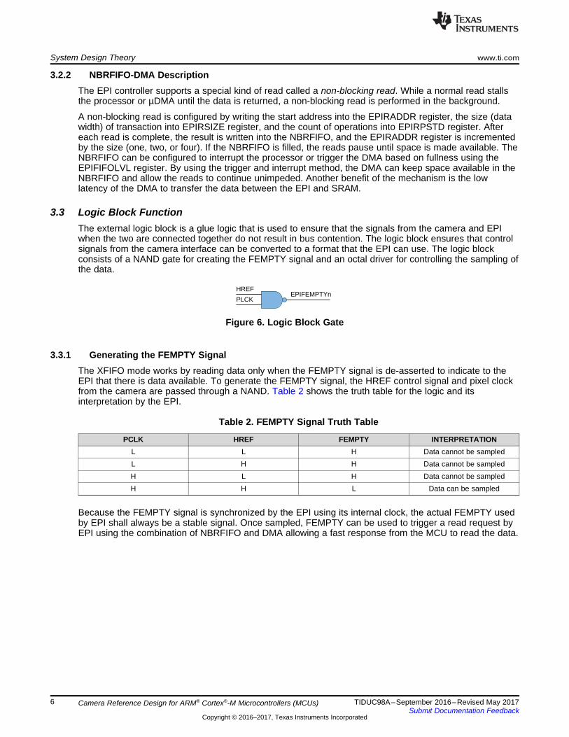
3.2.1 XFIFO Mode DescriptionThe XFIFO mode uses 8- or 16-bits of data, removes address latch enable (ALE), addresses pins, andoptionally adds external XFIFO, FFULL, and FEMPTY flag inputs. This submode provides the data side ofthe normal host-bus interface but is paced by the FIFO control signals. An important consideration is thatthe XFIFO, FFULL, and FEMPTY control signals may stall the interface and could have an impact onblocking read latency from the processor or µDMA.
For this design the read path for acquiring data from the camera is used, and the XFIFO and FEMPTYsignals are used for indicating the EPI when valid data from the camera is available. As shown in Figure 5,the read of the data is triggered only when the FEMPTY signal is asserted low. Once the EPI samples theFEMPTY low, a read can be initiated by the MCU (CPU or DMA) to read the data.
Figure 5. XFIFO Read Timing Diagram
HREF
PLCKEPIFEMPTYn
System Design Theory www.ti.com
6 TIDUC98A–September 2016–Revised May 2017Submit Documentation Feedback
Copyright © 2016–2017, Texas Instruments Incorporated
Camera Reference Design for ARM® Cortex®-M Microcontrollers (MCUs)
3.2.2 NBRFIFO-DMA DescriptionThe EPI controller supports a special kind of read called a non-blocking read. While a normal read stallsthe processor or µDMA until the data is returned, a non-blocking read is performed in the background.
A non-blocking read is configured by writing the start address into the EPIRADDR register, the size (datawidth) of transaction into EPIRSIZE register, and the count of operations into EPIRPSTD register. Aftereach read is complete, the result is written into the NBRFIFO, and the EPIRADDR register is incrementedby the size (one, two, or four). If the NBRFIFO is filled, the reads pause until space is made available. TheNBRFIFO can be configured to interrupt the processor or trigger the DMA based on fullness using theEPIFIFOLVL register. By using the trigger and interrupt method, the DMA can keep space available in theNBRFIFO and allow the reads to continue unimpeded. Another benefit of the mechanism is the lowlatency of the DMA to transfer the data between the EPI and SRAM.
3.3 Logic Block FunctionThe external logic block is a glue logic that is used to ensure that the signals from the camera and EPIwhen the two are connected together do not result in bus contention. The logic block ensures that controlsignals from the camera interface can be converted to a format that the EPI can use. The logic blockconsists of a NAND gate for creating the FEMPTY signal and an octal driver for controlling the sampling ofthe data.
Figure 6. Logic Block Gate
3.3.1 Generating the FEMPTY SignalThe XFIFO mode works by reading data only when the FEMPTY signal is de-asserted to indicate to theEPI that there is data available. To generate the FEMPTY signal, the HREF control signal and pixel clockfrom the camera are passed through a NAND. Table 2 shows the truth table for the logic and itsinterpretation by the EPI.
Table 2. FEMPTY Signal Truth Table
PCLK HREF FEMPTY INTERPRETATIONL L H Data cannot be sampledL H H Data cannot be sampledH L H Data cannot be sampledH H L Data can be sampled
Because the FEMPTY signal is synchronized by the EPI using its internal clock, the actual FEMPTY usedby EPI shall always be a stable signal. Once sampled, FEMPTY can be used to trigger a read request byEPI using the combination of NBRFIFO and DMA allowing a fast response from the MCU to read the data.
www.ti.com System Design Theory
7TIDUC98A–September 2016–Revised May 2017Submit Documentation Feedback
Copyright © 2016–2017, Texas Instruments Incorporated
Camera Reference Design for ARM® Cortex®-M Microcontrollers (MCUs)
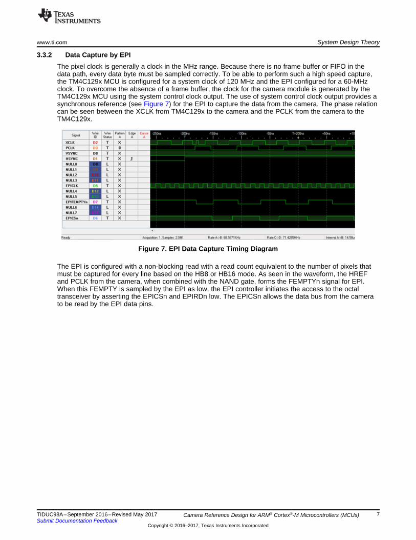
3.3.2 Data Capture by EPIThe pixel clock is generally a clock in the MHz range. Because there is no frame buffer or FIFO in thedata path, every data byte must be sampled correctly. To be able to perform such a high speed capture,the TM4C129x MCU is configured for a system clock of 120 MHz and the EPI configured for a 60-MHzclock. To overcome the absence of a frame buffer, the clock for the camera module is generated by theTM4C129x MCU using the system control clock output. The use of system control clock output provides asynchronous reference (see Figure 7) for the EPI to capture the data from the camera. The phase relationcan be seen between the XCLK from TM4C129x to the camera and the PCLK from the camera to theTM4C129x.
Figure 7. EPI Data Capture Timing Diagram
The EPI is configured with a non-blocking read with a read count equivalent to the number of pixels thatmust be captured for every line based on the HB8 or HB16 mode. As seen in the waveform, the HREFand PCLK from the camera, when combined with the NAND gate, forms the FEMPTYn signal for EPI.When this FEMPTY is sampled by the EPI as low, the EPI controller initiates the access to the octaltransceiver by asserting the EPICSn and EPIRDn low. The EPICSn allows the data bus from the camerato be read by the EPI data pins.
Getting Started Hardware and Software www.ti.com
8 TIDUC98A–September 2016–Revised May 2017Submit Documentation Feedback
Copyright © 2016–2017, Texas Instruments Incorporated
Camera Reference Design for ARM® Cortex®-M Microcontrollers (MCUs)
4 Getting Started Hardware and Software
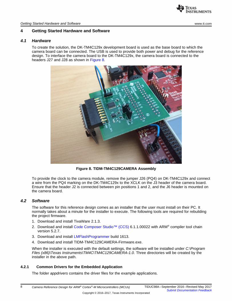
4.1 HardwareTo create the solution, the DK-TM4C129x development board is used as the base board to which thecamera board can be connected. The USB is used to provide both power and debug for the referencedesign. To interface the camera board to the DK-TM4C129x, the camera board is connected to theheaders J27 and J28 as shown in Figure 8.
Figure 8. TIDM-TM4C129CAMERA Assembly
To provide the clock to the camera module, remove the jumper J26 (PQ4) on DK-TM4C129x and connecta wire from the PQ4 marking on the DK-TM4C129x to the XCLK on the J3 header of the camera board.Ensure that the header J2 is connected between pin positions 1 and 2, and the J6 header is mounted onthe camera board.
4.2 SoftwareThe software for this reference design comes as an installer that the user must install on their PC. Itnormally takes about a minute for the installer to execute. The following tools are required for rebuildingthe project firmware.1. Download and install TivaWare 2.1.3.2. Download and install Code Composer Studio™ (CCS) 6.1.1.00022 with ARM® compiler tool chain
version 5.2.7.3. Download and install LMFlashProgrammer build 1613.4. Download and install TIDM-TM4C129CAMERA-Firmware.exe.
When the installer is executed with the default settings, the software will be installed under C:\ProgramFiles (x86)\Texas Instruments\TM4C\TM4C129CAMERA-1.0. Three directories will be created by theinstaller in the above path.
4.2.1 Common Drivers for the Embedded ApplicationThe folder appdrivers contains the driver files for the example applications.
LCDPanel
G3 B0
G4 B1
G5 B2
R0 B3
R1 B4
R2 G0
R3 G1
R4 G2
0 0
0 0
0 0
0 0
0 0
0 0
0 0
LCD Panel Data
0 0
LCDController
G3 B0
G4 B1
G5 B2
R0 B3
R1 B4
R2 G0
R3 G1
R4 G2
0 0
0 0
0 0
0 0
0 0
0 0
0 0
EPI Output 32-bit data
0 0
EPI
G3 B0
G4 B1
G5 B2
R0 B3
R1 B4
R2 G0
R3 G1
R4 G2
Camera Data
Byte-0
Byte-1
Byte-3
Byte-2
TivaWare Peripheral Driver Lib APl
Dktm4c129_cameralfr
Cameradriver
LCD driver
www.ti.com Getting Started Hardware and Software
9TIDUC98A–September 2016–Revised May 2017Submit Documentation Feedback
Copyright © 2016–2017, Texas Instruments Incorporated
Camera Reference Design for ARM® Cortex®-M Microcontrollers (MCUs)
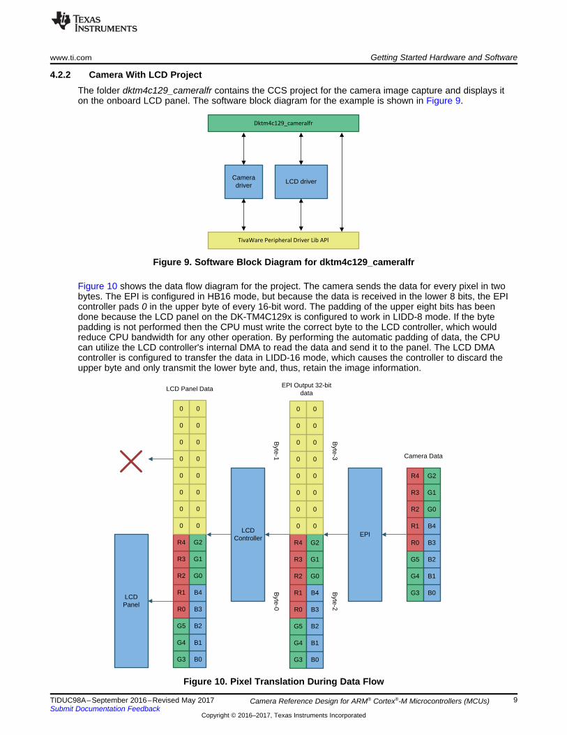
4.2.2 Camera With LCD ProjectThe folder dktm4c129_cameralfr contains the CCS project for the camera image capture and displays iton the onboard LCD panel. The software block diagram for the example is shown in Figure 9.
Figure 9. Software Block Diagram for dktm4c129_cameralfr
Figure 10 shows the data flow diagram for the project. The camera sends the data for every pixel in twobytes. The EPI is configured in HB16 mode, but because the data is received in the lower 8 bits, the EPIcontroller pads 0 in the upper byte of every 16-bit word. The padding of the upper eight bits has beendone because the LCD panel on the DK-TM4C129x is configured to work in LIDD-8 mode. If the bytepadding is not performed then the CPU must write the correct byte to the LCD controller, which wouldreduce CPU bandwidth for any other operation. By performing the automatic padding of data, the CPUcan utilize the LCD controller's internal DMA to read the data and send it to the panel. The LCD DMAcontroller is configured to transfer the data in LIDD-16 mode, which causes the controller to discard theupper byte and only transmit the lower byte and, thus, retain the image information.
Figure 10. Pixel Translation During Data Flow
TivaWare Peripheral Driver Lib APl
enet_camera_server
IwlpCameradriver
Brightness Control
Graphics Library(grlib)
Getting Started Hardware and Software www.ti.com
10 TIDUC98A–September 2016–Revised May 2017Submit Documentation Feedback
Copyright © 2016–2017, Texas Instruments Incorporated
Camera Reference Design for ARM® Cortex®-M Microcontrollers (MCUs)
Since the pixel data captured per line is buffered by the LCD controller’s internal FIFO, the SRAMrequirement is limited to only one line of data capture, that is, 320 pixels × (2 bytes of pixel information + 2byte of padded data) or 1280 bytes.
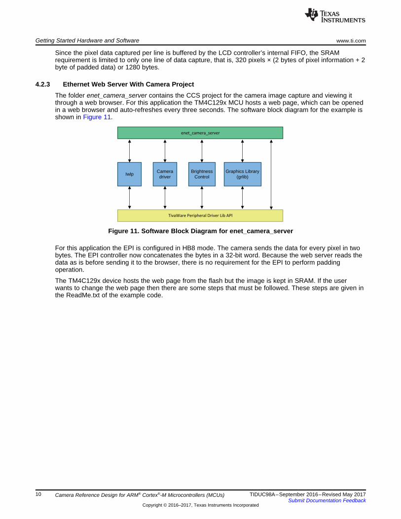
4.2.3 Ethernet Web Server With Camera ProjectThe folder enet_camera_server contains the CCS project for the camera image capture and viewing itthrough a web browser. For this application the TM4C129x MCU hosts a web page, which can be openedin a web browser and auto-refreshes every three seconds. The software block diagram for the example isshown in Figure 11.
Figure 11. Software Block Diagram for enet_camera_server
For this application the EPI is configured in HB8 mode. The camera sends the data for every pixel in twobytes. The EPI controller now concatenates the bytes in a 32-bit word. Because the web server reads thedata as is before sending it to the browser, there is no requirement for the EPI to perform paddingoperation.
The TM4C129x device hosts the web page from the flash but the image is kept in SRAM. If the userwants to change the web page then there are some steps that must be followed. These steps are given inthe ReadMe.txt of the example code.
www.ti.com Testing and Results
11TIDUC98A–September 2016–Revised May 2017Submit Documentation Feedback
Copyright © 2016–2017, Texas Instruments Incorporated
Camera Reference Design for ARM® Cortex®-M Microcontrollers (MCUs)
5 Testing and Results
5.1 Test SetupNow that the board has been setup for downloading the application firmware and the user has installedthe application software, this section will elaborate on how to import, build, and run the applicationfirmware for voice call.
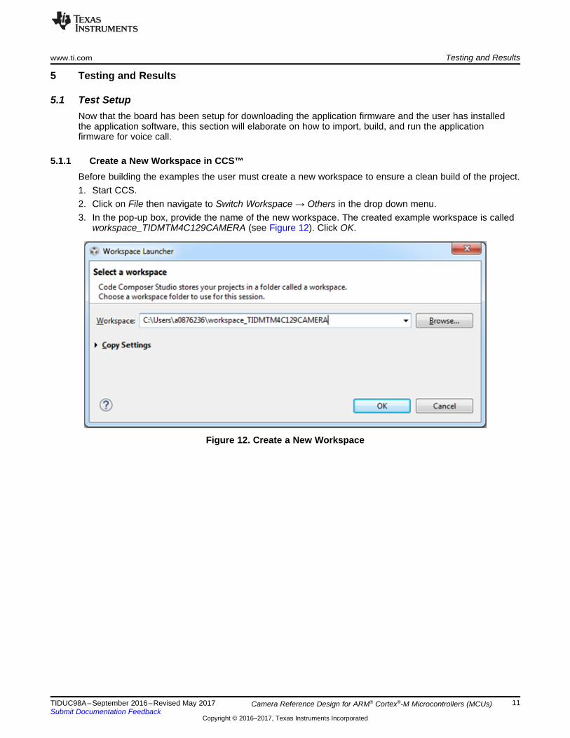
5.1.1 Create a New Workspace in CCS™Before building the examples the user must create a new workspace to ensure a clean build of the project.1. Start CCS.2. Click on File then navigate to Switch Workspace → Others in the drop down menu.3. In the pop-up box, provide the name of the new workspace. The created example workspace is called
workspace_TIDMTM4C129CAMERA (see Figure 12). Click OK.
Figure 12. Create a New Workspace
Testing and Results www.ti.com
12 TIDUC98A–September 2016–Revised May 2017Submit Documentation Feedback
Copyright © 2016–2017, Texas Instruments Incorporated
Camera Reference Design for ARM® Cortex®-M Microcontrollers (MCUs)
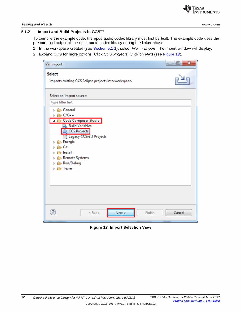
5.1.2 Import and Build Projects in CCS™To compile the example code, the opus audio codec library must first be built. The example code uses theprecompiled output of the opus audio codec library during the linker phase.1. In the workspace created (see Section 5.1.1), select File → Import. The import window will display.2. Expand CCS for more options. Click CCS Projects. Click on Next (see Figure 13).
Figure 13. Import Selection View
www.ti.com Testing and Results
13TIDUC98A–September 2016–Revised May 2017Submit Documentation Feedback
Copyright © 2016–2017, Texas Instruments Incorporated
Camera Reference Design for ARM® Cortex®-M Microcontrollers (MCUs)
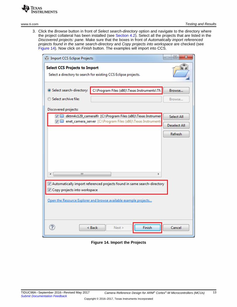
3. Click the Browse button in front of Select search-directory option and navigate to the directory wherethe project collateral has been installed (see Section 4.2). Select all the projects that are listed in theDiscovered projects: pane. Make sure that the boxes in front of Automatically import referencedprojects found in the same search-directory and Copy projects into workspace are checked (seeFigure 14). Now click on Finish button. The examples will import into CCS.
Figure 14. Import the Projects
Testing and Results www.ti.com
14 TIDUC98A–September 2016–Revised May 2017Submit Documentation Feedback
Copyright © 2016–2017, Texas Instruments Incorporated
Camera Reference Design for ARM® Cortex®-M Microcontrollers (MCUs)
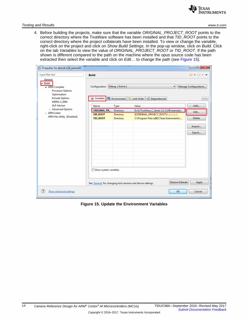
4. Before building the projects, make sure that the variable ORIGINAL_PROJECT_ROOT points to thecorrect directory where the TivaWare software has been installed and that TID_ROOT points to thecorrect directory where the project collaterals have been installed. To view or change the variable,right-click on the project and click on Show Build Settings. In the pop-up window, click on Build. Clickon the tab Variables to view the value of ORIGINAL_PROJECT_ROOT or TID_ROOT. If the pathshown is different compared to the path on the machine where the opus source code has beenextracted then select the variable and click on Edit… to change the path (see Figure 15).
Figure 15. Update the Environment Variables
www.ti.com Testing and Results
15TIDUC98A–September 2016–Revised May 2017Submit Documentation Feedback
Copyright © 2016–2017, Texas Instruments Incorporated
Camera Reference Design for ARM® Cortex®-M Microcontrollers (MCUs)
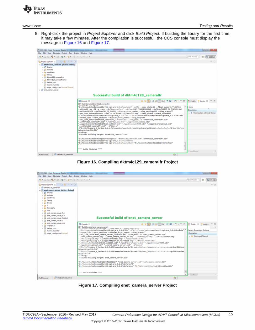
5. Right-click the project in Project Explorer and click Build Project. If building the library for the first time,it may take a few minutes. After the compilation is successful, the CCS console must display themessage in Figure 16 and Figure 17.
Figure 16. Compiling dktm4c129_cameralfr Project
Figure 17. Compiling enet_camera_server Project
Testing and Results www.ti.com
16 TIDUC98A–September 2016–Revised May 2017Submit Documentation Feedback
Copyright © 2016–2017, Texas Instruments Incorporated
Camera Reference Design for ARM® Cortex®-M Microcontrollers (MCUs)
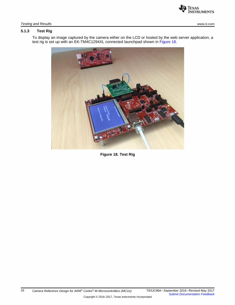
5.1.3 Test RigTo display an image captured by the camera either on the LCD or hosted by the web server application, atest rig is set up with an EK-TM4C1294XL connected launchpad shown in Figure 18.
Figure 18. Test Rig
www.ti.com Testing and Results
17TIDUC98A–September 2016–Revised May 2017Submit Documentation Feedback
Copyright © 2016–2017, Texas Instruments Incorporated
Camera Reference Design for ARM® Cortex®-M Microcontrollers (MCUs)
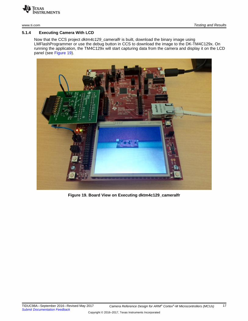
5.1.4 Executing Camera With LCDNow that the CCS project dktm4c129_cameralfr is built, download the binary image usingLMFlashProgrammer or use the debug button in CCS to download the image to the DK-TM4C129x. Onrunning the application, the TM4C129x will start capturing data from the camera and display it on the LCDpanel (see Figure 19).
Figure 19. Board View on Executing dktm4c129_cameralfr
Testing and Results www.ti.com
18 TIDUC98A–September 2016–Revised May 2017Submit Documentation Feedback
Copyright © 2016–2017, Texas Instruments Incorporated
Camera Reference Design for ARM® Cortex®-M Microcontrollers (MCUs)
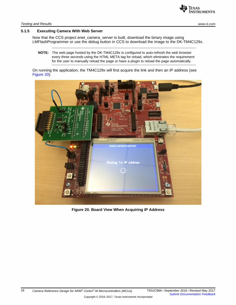
5.1.5 Executing Camera With Web ServerNow that the CCS project enet_camera_server is built, download the binary image usingLMFlashProgrammer or use the debug button in CCS to download the image to the DK-TM4C129x.
NOTE: The web page hosted by the DK-TM4C129x is configured to auto-refresh the web browserevery three seconds using the HTML META tag for reload, which eliminates the requirementfor the user to manually reload the page or have a plugin to reload the page automatically.
On running the application, the TM4C129x will first acquire the link and then an IP address (seeFigure 20).
Figure 20. Board View When Acquiring IP Address
www.ti.com Testing and Results
19TIDUC98A–September 2016–Revised May 2017Submit Documentation Feedback
Copyright © 2016–2017, Texas Instruments Incorporated
Camera Reference Design for ARM® Cortex®-M Microcontrollers (MCUs)
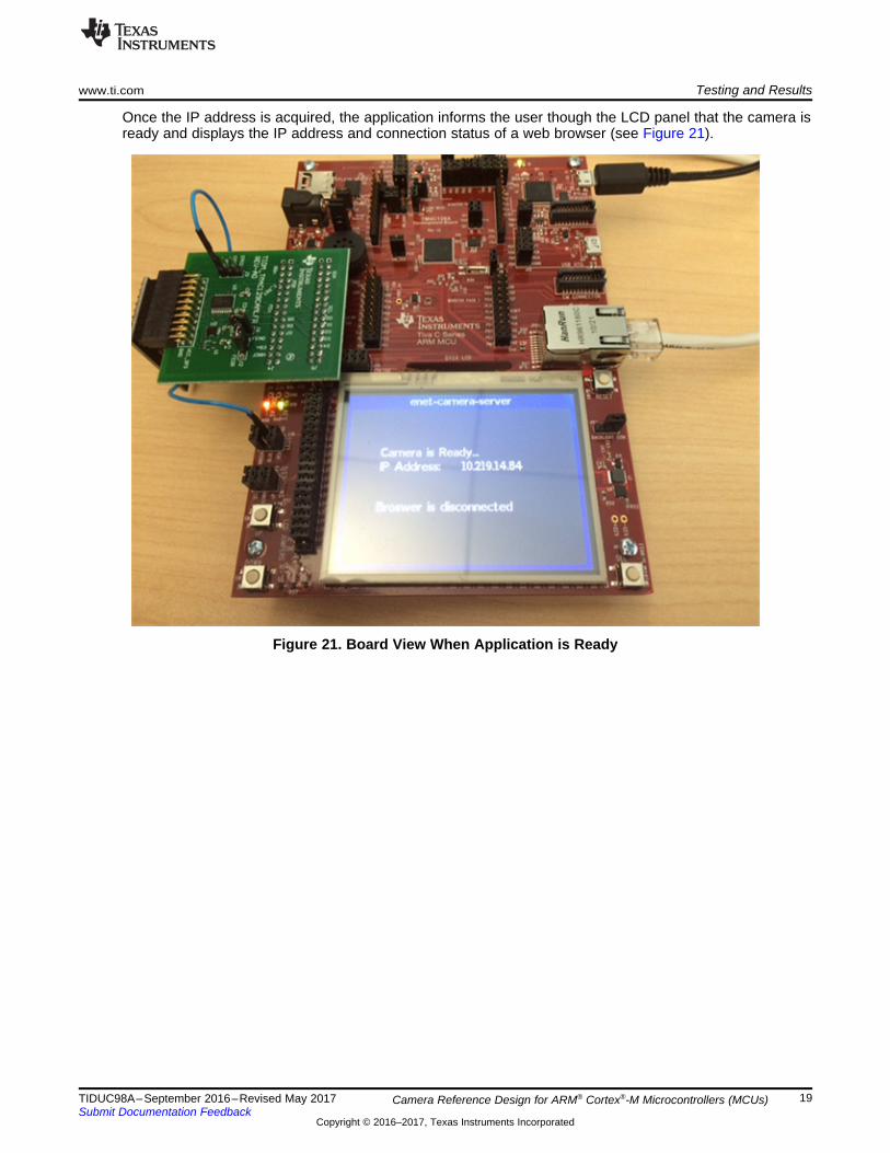
Once the IP address is acquired, the application informs the user though the LCD panel that the camera isready and displays the IP address and connection status of a web browser (see Figure 21).
Figure 21. Board View When Application is Ready
Testing and Results www.ti.com
20 TIDUC98A–September 2016–Revised May 2017Submit Documentation Feedback
Copyright © 2016–2017, Texas Instruments Incorporated
Camera Reference Design for ARM® Cortex®-M Microcontrollers (MCUs)
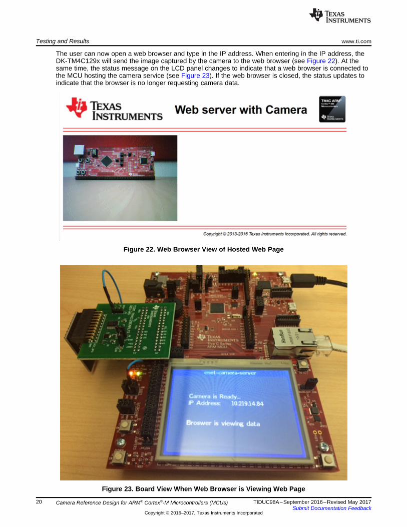
The user can now open a web browser and type in the IP address. When entering in the IP address, theDK-TM4C129x will send the image captured by the camera to the web browser (see Figure 22). At thesame time, the status message on the LCD panel changes to indicate that a web browser is connected tothe MCU hosting the camera service (see Figure 23). If the web browser is closed, the status updates toindicate that the browser is no longer requesting camera data.
Figure 22. Web Browser View of Hosted Web Page
Figure 23. Board View When Web Browser is Viewing Web Page
www.ti.com Testing and Results
21TIDUC98A–September 2016–Revised May 2017Submit Documentation Feedback
Copyright © 2016–2017, Texas Instruments Incorporated
Camera Reference Design for ARM® Cortex®-M Microcontrollers (MCUs)
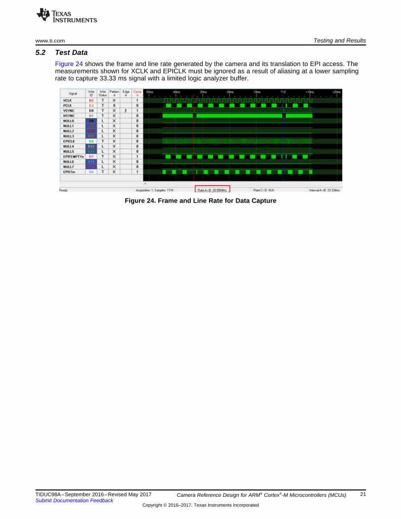
5.2 Test DataFigure 24 shows the frame and line rate generated by the camera and its translation to EPI access. Themeasurements shown for XCLK and EPICLK must be ignored as a result of aliasing at a lower samplingrate to capture 33.33 ms signal with a limited logic analyzer buffer.
Figure 24. Frame and Line Rate for Data Capture
Design Files www.ti.com
22 TIDUC98A–September 2016–Revised May 2017Submit Documentation Feedback
Copyright © 2016–2017, Texas Instruments Incorporated
Camera Reference Design for ARM® Cortex®-M Microcontrollers (MCUs)
6 Design Files
6.1 SchematicsTo download the schematics, see the design files at TIDM-TM4C129CAMERA.
6.2 Bill of MaterialsTo download the bill of materials (BOM), see the design files at TIDM-TM4C129CAMERA.
6.3 PCB Layout Recommendations
6.3.1 Layout PrintsTo download the layer plots, see the design files at TIDM-TM4C129CAMERA.
6.4 Altium ProjectTo download the Altium project files, see the design files at TIDM-TM4C129CAMERA.
6.5 Gerber FilesTo download the Gerber files, see the design files at TIDM-TM4C129CAMERA.
6.6 Assembly DrawingsTo download the assembly drawings, see the design files at TIDM-TM4C129CAMERA.
7 Software FilesTo download the software files, see the design files at TIDM-TM4C129CAMERA.
8 References
1. Wave Share, 0v9655 Camera Board.
8.1 TrademarksAll trademarks are the property of their respective owners.
9 About the AuthorAMIT ASHARA is an application engineer and Member Group Technical staff member at TexasInstruments. He works on developing applications for the TM4C12x family of high-performance MCUs.Amit brings extensive experience in high-speed digital and MCU system-level design expertise to this role.Amit earned his Bachelor of Engineering (BE) from the University of Pune in India.
www.ti.com Revision A History
23TIDUC98A–September 2016–Revised May 2017Submit Documentation Feedback
Copyright © 2016–2017, Texas Instruments Incorporated
Revision History
Revision A HistoryNOTE: Page numbers for previous revisions may differ from page numbers in the current version.
Changes from Original (September 2016) to A Revision ............................................................................................... Page
• Changed location of Section 1 (previously Section 1.1).............................................................................. 2• Changed location of Section 1.1 (previously Section 1.2). .......................................................................... 2• Changed Figure 2. ........................................................................................................................ 3
IMPORTANT NOTICE FOR TI DESIGN INFORMATION AND RESOURCES
Texas Instruments Incorporated (‘TI”) technical, application or other design advice, services or information, including, but not limited to,reference designs and materials relating to evaluation modules, (collectively, “TI Resources”) are intended to assist designers who aredeveloping applications that incorporate TI products; by downloading, accessing or using any particular TI Resource in any way, you(individually or, if you are acting on behalf of a company, your company) agree to use it solely for this purpose and subject to the terms ofthis Notice.TI’s provision of TI Resources does not expand or otherwise alter TI’s applicable published warranties or warranty disclaimers for TIproducts, and no additional obligations or liabilities arise from TI providing such TI Resources. TI reserves the right to make corrections,enhancements, improvements and other changes to its TI Resources.You understand and agree that you remain responsible for using your independent analysis, evaluation and judgment in designing yourapplications and that you have full and exclusive responsibility to assure the safety of your applications and compliance of your applications(and of all TI products used in or for your applications) with all applicable regulations, laws and other applicable requirements. Yourepresent that, with respect to your applications, you have all the necessary expertise to create and implement safeguards that (1)anticipate dangerous consequences of failures, (2) monitor failures and their consequences, and (3) lessen the likelihood of failures thatmight cause harm and take appropriate actions. You agree that prior to using or distributing any applications that include TI products, youwill thoroughly test such applications and the functionality of such TI products as used in such applications. TI has not conducted anytesting other than that specifically described in the published documentation for a particular TI Resource.You are authorized to use, copy and modify any individual TI Resource only in connection with the development of applications that includethe TI product(s) identified in such TI Resource. NO OTHER LICENSE, EXPRESS OR IMPLIED, BY ESTOPPEL OR OTHERWISE TOANY OTHER TI INTELLECTUAL PROPERTY RIGHT, AND NO LICENSE TO ANY TECHNOLOGY OR INTELLECTUAL PROPERTYRIGHT OF TI OR ANY THIRD PARTY IS GRANTED HEREIN, including but not limited to any patent right, copyright, mask work right, orother intellectual property right relating to any combination, machine, or process in which TI products or services are used. Informationregarding or referencing third-party products or services does not constitute a license to use such products or services, or a warranty orendorsement thereof. Use of TI Resources may require a license from a third party under the patents or other intellectual property of thethird party, or a license from TI under the patents or other intellectual property of TI.TI RESOURCES ARE PROVIDED “AS IS” AND WITH ALL FAULTS. TI DISCLAIMS ALL OTHER WARRANTIES ORREPRESENTATIONS, EXPRESS OR IMPLIED, REGARDING TI RESOURCES OR USE THEREOF, INCLUDING BUT NOT LIMITED TOACCURACY OR COMPLETENESS, TITLE, ANY EPIDEMIC FAILURE WARRANTY AND ANY IMPLIED WARRANTIES OFMERCHANTABILITY, FITNESS FOR A PARTICULAR PURPOSE, AND NON-INFRINGEMENT OF ANY THIRD PARTY INTELLECTUALPROPERTY RIGHTS.TI SHALL NOT BE LIABLE FOR AND SHALL NOT DEFEND OR INDEMNIFY YOU AGAINST ANY CLAIM, INCLUDING BUT NOTLIMITED TO ANY INFRINGEMENT CLAIM THAT RELATES TO OR IS BASED ON ANY COMBINATION OF PRODUCTS EVEN IFDESCRIBED IN TI RESOURCES OR OTHERWISE. IN NO EVENT SHALL TI BE LIABLE FOR ANY ACTUAL, DIRECT, SPECIAL,COLLATERAL, INDIRECT, PUNITIVE, INCIDENTAL, CONSEQUENTIAL OR EXEMPLARY DAMAGES IN CONNECTION WITH ORARISING OUT OF TI RESOURCES OR USE THEREOF, AND REGARDLESS OF WHETHER TI HAS BEEN ADVISED OF THEPOSSIBILITY OF SUCH DAMAGES.You agree to fully indemnify TI and its representatives against any damages, costs, losses, and/or liabilities arising out of your non-compliance with the terms and provisions of this Notice.This Notice applies to TI Resources. Additional terms apply to the use and purchase of certain types of materials, TI products and services.These include; without limitation, TI’s standard terms for semiconductor products http://www.ti.com/sc/docs/stdterms.htm), evaluationmodules, and samples (http://www.ti.com/sc/docs/sampterms.htm).
Mailing Address: Texas Instruments, Post Office Box 655303, Dallas, Texas 75265Copyright © 2017, Texas Instruments Incorporated