tidueu4 | ti.com - semiconductor company | ti.com
TRANSCRIPT
22 µF
+
±
22 µH
19VDC
ControlLogic
+ ±
VREF
22 µFTVS3300
TPS54202
16.8 VDC
FB
TLV9001
1TIDUEU4–November 2019Submit Documentation Feedback
Copyright © 2019, Texas Instruments Incorporated
Cost-Optimized Battery Charger Reference Design With 1.0-A Current and±1.5% Voltage Accuracy
Design Guide: TIDA-010075Cost-Optimized Battery Charger Reference Design With1.0-A Current and ±1.5% Voltage Accuracy
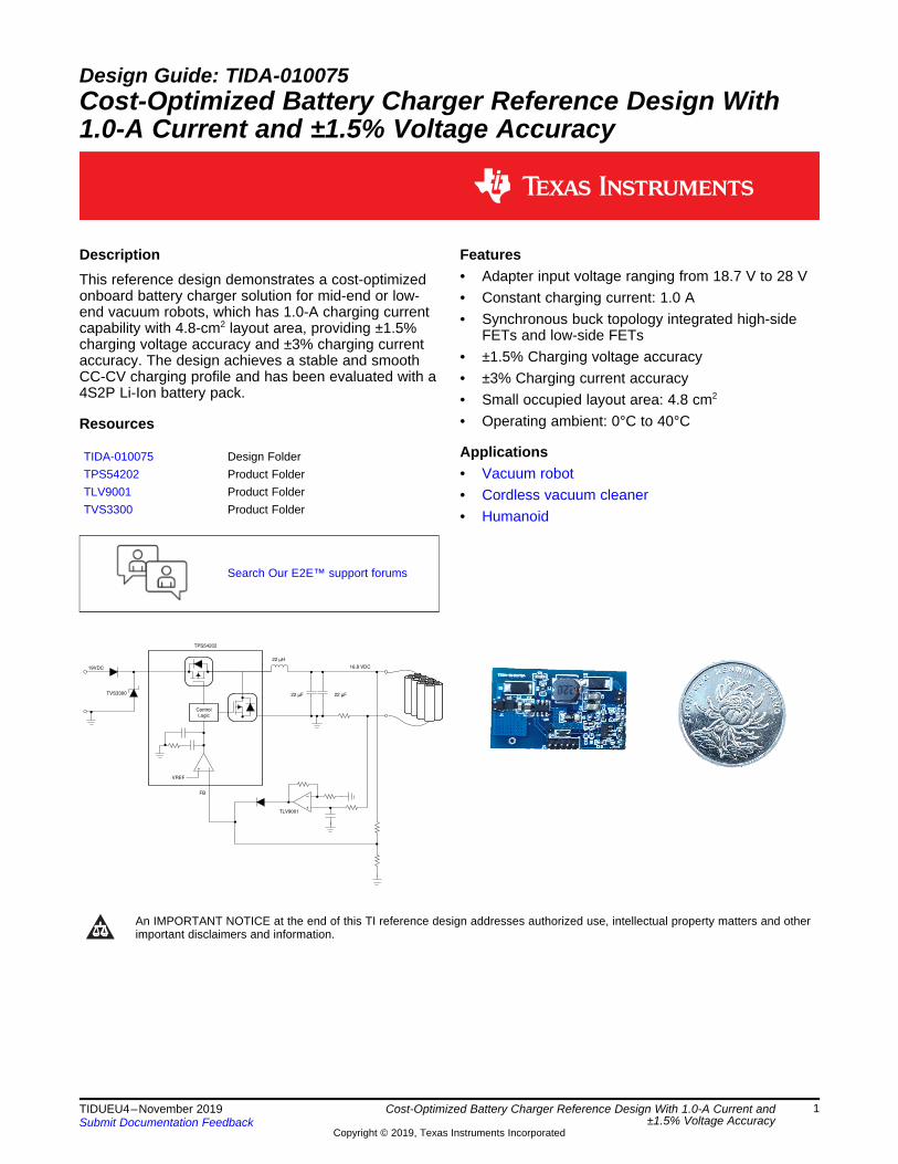
DescriptionThis reference design demonstrates a cost-optimizedonboard battery charger solution for mid-end or low-end vacuum robots, which has 1.0-A charging currentcapability with 4.8-cm2 layout area, providing ±1.5%charging voltage accuracy and ±3% charging currentaccuracy. The design achieves a stable and smoothCC-CV charging profile and has been evaluated with a4S2P Li-Ion battery pack.
Resources
TIDA-010075 Design FolderTPS54202 Product FolderTLV9001 Product FolderTVS3300 Product Folder
Search Our E2E™ support forums
Features• Adapter input voltage ranging from 18.7 V to 28 V• Constant charging current: 1.0 A• Synchronous buck topology integrated high-side
FETs and low-side FETs• ±1.5% Charging voltage accuracy• ±3% Charging current accuracy• Small occupied layout area: 4.8 cm2
• Operating ambient: 0°C to 40°C
Applications• Vacuum robot• Cordless vacuum cleaner• Humanoid
An IMPORTANT NOTICE at the end of this TI reference design addresses authorized use, intellectual property matters and otherimportant disclaimers and information.
100 �F
PWMCompensator
Error
REF
�+
±
SEL
ADC
ADC
MUX
+
±
+
±
Totem-PoleDriver
100 µH
19VDC
System Description www.ti.com
2 TIDUEU4–November 2019Submit Documentation Feedback
Copyright © 2019, Texas Instruments Incorporated
Cost-Optimized Battery Charger Reference Design With 1.0-A Current and±1.5% Voltage Accuracy
1 System DescriptionA vacuum robot, also called a robotic vacuum cleaner, which has been around for about 23 years, isgetting more intelligent and automatic. There is an expectation that robots should be able to do a fullcleaning cycle before needing to charge again. With more features added in a vacuum robot, such asmopping, audio interaction, navigating thick carpet, and climbing higher thresholds, the power requirementfor a full cleaning cycle is increasing, so the battery capacity is becoming bigger, typically from 2600 mAhto 5200 mAh.
Meanwhile, this also increase the requirements for the battery charger. The following items list the generalrequirements for an onboard charger, which means the charger circuit is implemented on the main boardof the robot, which is widely used for almost all brands of vacuum robots around the world:• High charging current• Cost effective• Small size• High charging voltage accuracy• High charging current accuracy• Easy to design
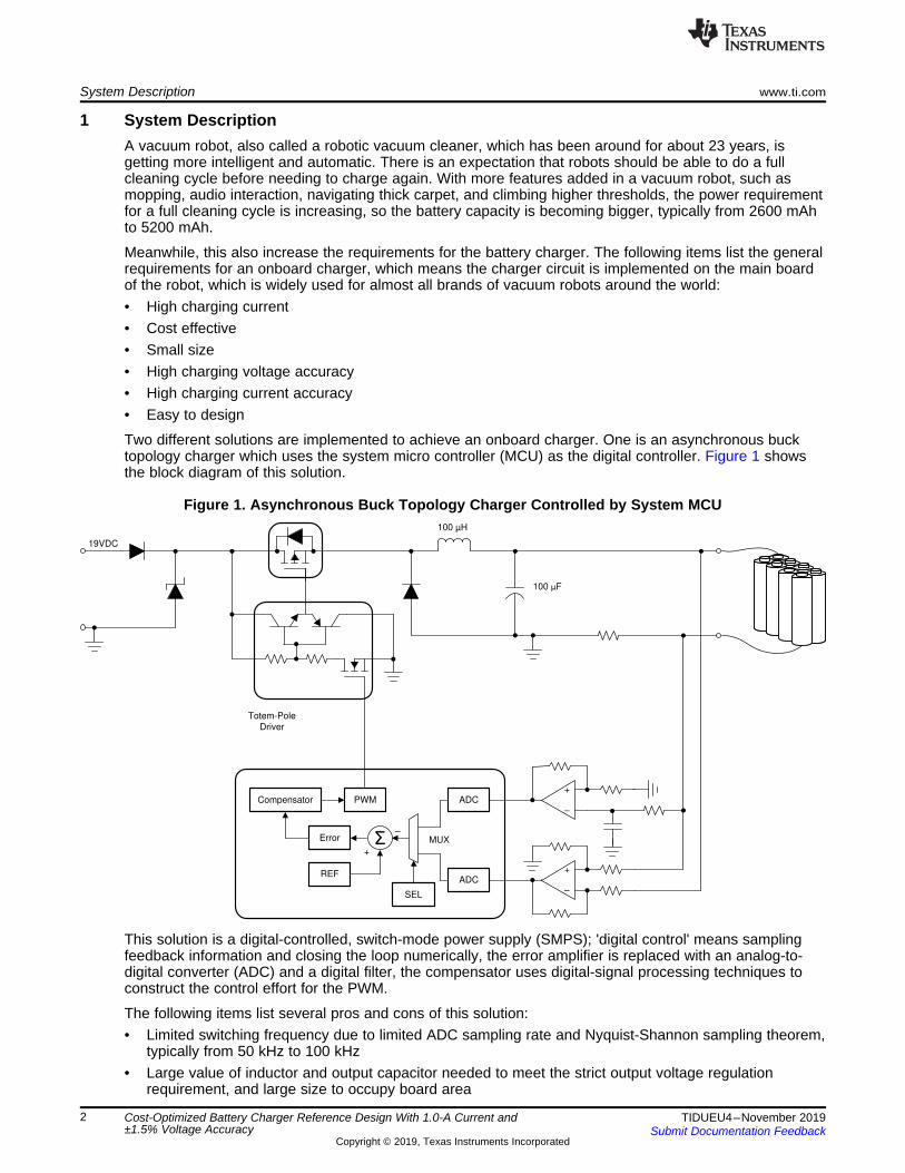
Two different solutions are implemented to achieve an onboard charger. One is an asynchronous bucktopology charger which uses the system micro controller (MCU) as the digital controller. Figure 1 showsthe block diagram of this solution.
Figure 1. Asynchronous Buck Topology Charger Controlled by System MCU
This solution is a digital-controlled, switch-mode power supply (SMPS); 'digital control' means samplingfeedback information and closing the loop numerically, the error amplifier is replaced with an analog-to-digital converter (ADC) and a digital filter, the compensator uses digital-signal processing techniques toconstruct the control effort for the PWM.
The following items list several pros and cons of this solution:• Limited switching frequency due to limited ADC sampling rate and Nyquist-Shannon sampling theorem,
typically from 50 kHz to 100 kHz• Large value of inductor and output capacitor needed to meet the strict output voltage regulation
requirement, and large size to occupy board area
6.8 µH
19 VDC
BQ24xxx
Standalone
/I2C
/SMBUS
10 �F 10 �F
VFB
16.8 VDC
SRP
SRN
TVS3300
www.ti.com System Description
3TIDUEU4–November 2019Submit Documentation Feedback
Copyright © 2019, Texas Instruments Incorporated
Cost-Optimized Battery Charger Reference Design With 1.0-A Current and±1.5% Voltage Accuracy
• Low efficiency due to the asynchronous buck topology and low thermal performance especiallyaffected by the power dissipation of the free-wheeling diode
• Complex digital-signal processing techniques to achieve a stable closed loop and keep multiple MCUresources occupied, such as memory, PWM, ALU, ADC, the charging voltage accuracy depends onthe accuracy of the reference voltage for ADC, and the charging voltage accuracy is around ±3%.
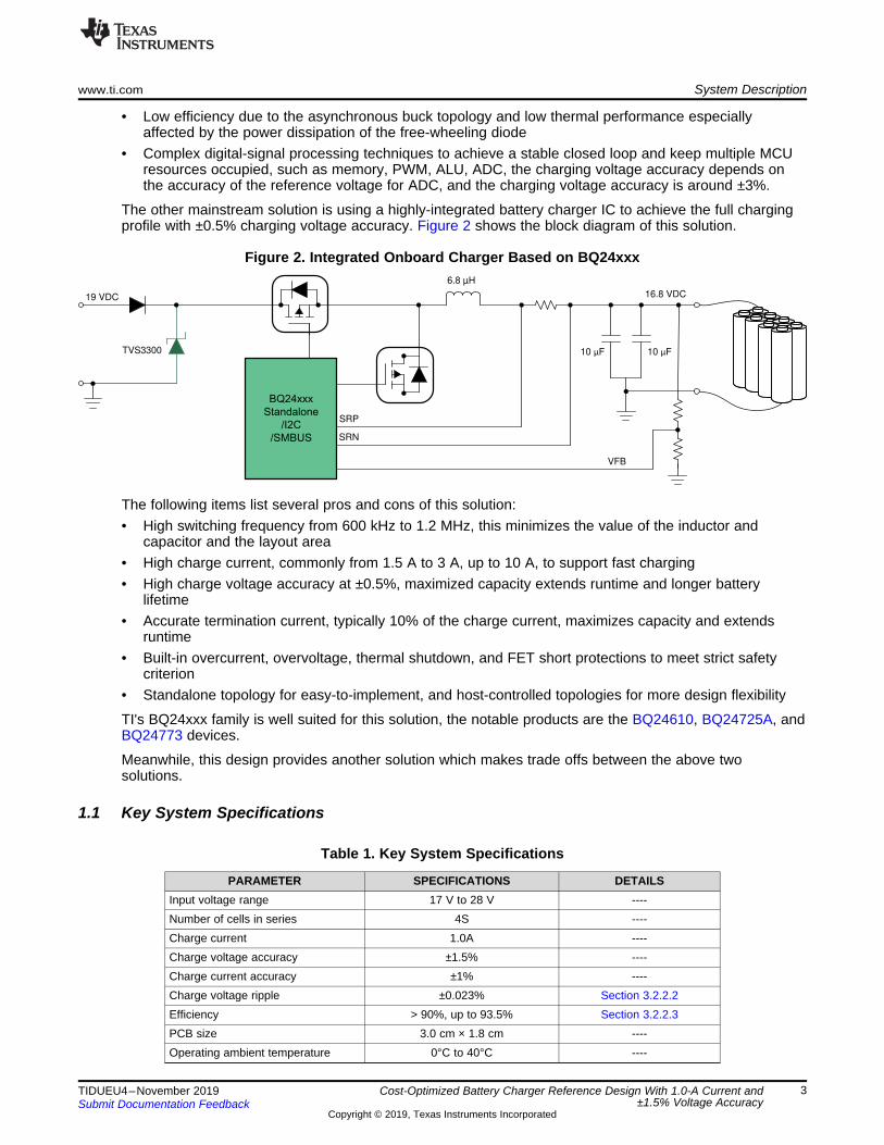
The other mainstream solution is using a highly-integrated battery charger IC to achieve the full chargingprofile with ±0.5% charging voltage accuracy. Figure 2 shows the block diagram of this solution.
Figure 2. Integrated Onboard Charger Based on BQ24xxx
The following items list several pros and cons of this solution:• High switching frequency from 600 kHz to 1.2 MHz, this minimizes the value of the inductor and
capacitor and the layout area• High charge current, commonly from 1.5 A to 3 A, up to 10 A, to support fast charging• High charge voltage accuracy at ±0.5%, maximized capacity extends runtime and longer battery
lifetime• Accurate termination current, typically 10% of the charge current, maximizes capacity and extends
runtime• Built-in overcurrent, overvoltage, thermal shutdown, and FET short protections to meet strict safety
criterion• Standalone topology for easy-to-implement, and host-controlled topologies for more design flexibility
TI's BQ24xxx family is well suited for this solution, the notable products are the BQ24610, BQ24725A, andBQ24773 devices.
Meanwhile, this design provides another solution which makes trade offs between the above twosolutions.
1.1 Key System Specifications
Table 1. Key System Specifications
PARAMETER SPECIFICATIONS DETAILSInput voltage range 17 V to 28 V ----Number of cells in series 4S ----Charge current 1.0A ----Charge voltage accuracy ±1.5% ----Charge current accuracy ±1% ----Charge voltage ripple ±0.023% Section 3.2.2.2Efficiency > 90%, up to 93.5% Section 3.2.2.3PCB size 3.0 cm × 1.8 cm ----Operating ambient temperature 0°C to 40°C ----

22 µF
+
±
22 µH
19VDC
ControlLogic
+ ±
VREF
22 µFTVS3300
TPS54202
16.8 VDC
FB
TLV9001
System Overview www.ti.com
4 TIDUEU4–November 2019Submit Documentation Feedback
Copyright © 2019, Texas Instruments Incorporated
Cost-Optimized Battery Charger Reference Design With 1.0-A Current and±1.5% Voltage Accuracy
2 System Overview
2.1 Block Diagram
Figure 3. TIDA-010075 Block Diagram
2.2 Design ConsiderationsThis reference design attempts to optimize the system BOM cost and charge current capacity by trading-off the charge voltage accuracy, which affects the utilizable of the battery. This solution achieves a batterycharger based on a synchronous buck converter - the TPS54202 device integrates two switching FETs,internal loop compensation, and employs the SOT-23 package achieving high power density and offeringa small footprint on the PCB. The analog control eliminates the MCU resources and software workload,which is easier to implement and decreases the design cycle. This solution achieves a simple chargingprofile - constant voltage stage and constant current stage using the TLV9001 device which contributeshigh current-sensing accuracy.
BOOT
SW
VINEN
-
+
+
LS MOSFET
Current Limit
OscillatorMaximum
Clamp
Overload
Recovery
Soft Start
Voltage
Reference
Slope
Compensation
HS MOSFET
Current
Comparator
Minimum Clamp
Pulse Skip
Power Stage
And
Dead time
Control
Logic
Boot UVLO
Boot Charge
UVLOThermal
Hiccup
Shutdown
Logic
ERROR AMPLIFIER
Regulator
VIN
-
+
OV comparator
0.596V
Current
Sense
Current
Sense
FB
GND
Hiccup
Shutdown
Hiccup
Shutdown
EN Compatator
Ip Ih
30 k:
2.2nF
2pF
Copyright © 2016, Texas Instruments Incorporated
www.ti.com System Overview
5TIDUEU4–November 2019Submit Documentation Feedback
Copyright © 2019, Texas Instruments Incorporated
Cost-Optimized Battery Charger Reference Design With 1.0-A Current and±1.5% Voltage Accuracy
2.3 Highlighted ProductsThe following subsections detail the highlighted products used in this reference design, including the keyfeatures for their selection. See their respective product data sheets for complete details on anyhighlighted device.
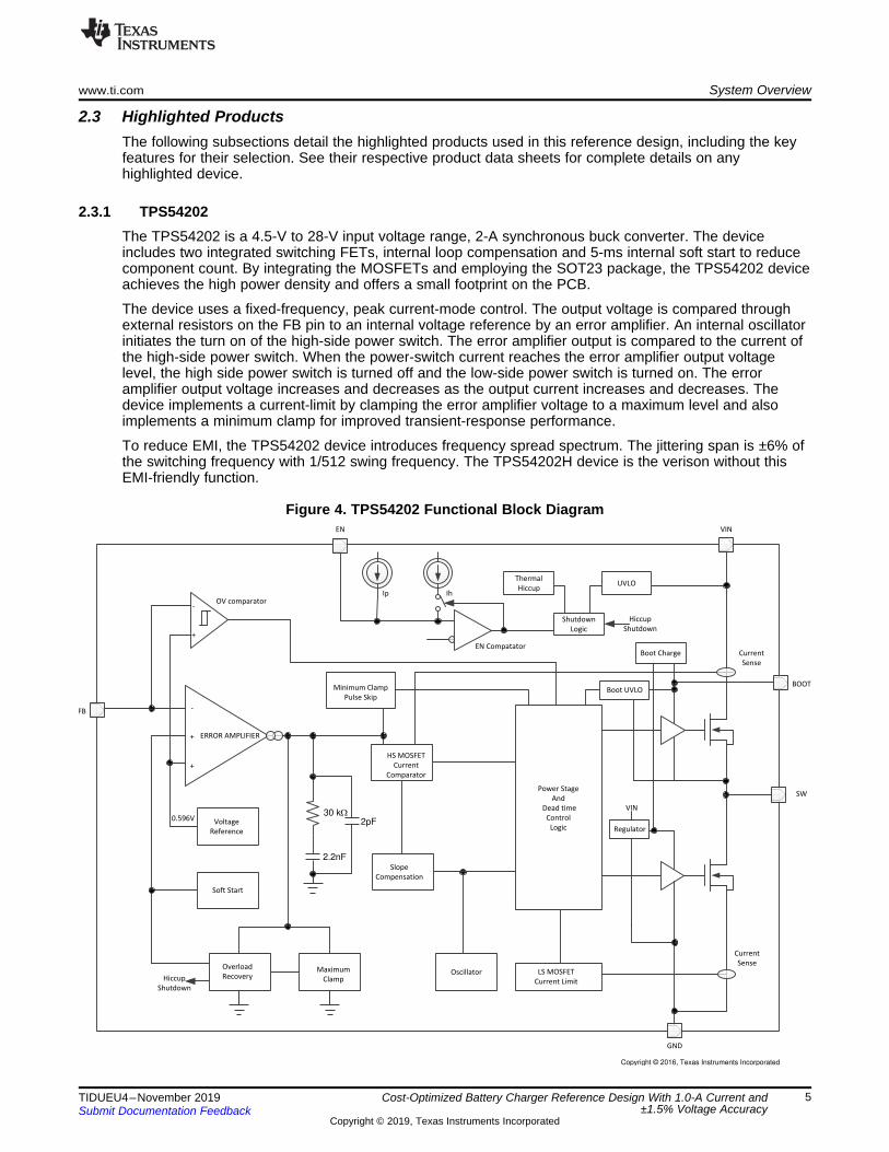
2.3.1 TPS54202The TPS54202 is a 4.5-V to 28-V input voltage range, 2-A synchronous buck converter. The deviceincludes two integrated switching FETs, internal loop compensation and 5-ms internal soft start to reducecomponent count. By integrating the MOSFETs and employing the SOT23 package, the TPS54202 deviceachieves the high power density and offers a small footprint on the PCB.
The device uses a fixed-frequency, peak current-mode control. The output voltage is compared throughexternal resistors on the FB pin to an internal voltage reference by an error amplifier. An internal oscillatorinitiates the turn on of the high-side power switch. The error amplifier output is compared to the current ofthe high-side power switch. When the power-switch current reaches the error amplifier output voltagelevel, the high side power switch is turned off and the low-side power switch is turned on. The erroramplifier output voltage increases and decreases as the output current increases and decreases. Thedevice implements a current-limit by clamping the error amplifier voltage to a maximum level and alsoimplements a minimum clamp for improved transient-response performance.
To reduce EMI, the TPS54202 device introduces frequency spread spectrum. The jittering span is ±6% ofthe switching frequency with 1/512 swing frequency. The TPS54202H device is the verison without thisEMI-friendly function.
Figure 4. TPS54202 Functional Block Diagram
System Overview www.ti.com
6 TIDUEU4–November 2019Submit Documentation Feedback
Copyright © 2019, Texas Instruments Incorporated
Cost-Optimized Battery Charger Reference Design With 1.0-A Current and±1.5% Voltage Accuracy
2.3.2 TLV9001The TLV9001 device is a single channel low-voltage operational amplifier (op amps) with rail-to-rail inputand output swing capabilities. This op amp provides a cost-effective solution for space-constrainedapplications and high capacitive-load drive is required. The capacitive-load drive of the TLV900x family is500 pF, and the resistive open loop output impedance makes stabilization easier with much highercapacitive loads.
The robust design of the TLV900x family simplifies circuit design. The op amps feature unity-gain stability,an integrated RFI and EMI rejection filter, and no-phase reversal in overdrive conditions.
Digital Core
Power Management and Supervisors
Port Data Multiplexer
NMOS
External FET Control and Sense
2
2
2
2
2
2
3
3
4
2
9
2
2
2
C_USB_TP/TN
C_USB_BP/BN
C_SBU1/2
C_CC1
C_CC2
VBUS
PP_5V0
VIN_3V3
RESETZMRESETHRESET
VOUT_3V3
LDO_3V3
LDO_1V8A
LDO_1V8D
LDO_BMC
BUSPOWERZ
R_OSC
GPIO1-9
I2C_SDA/SCL/IRQ1Z
I2C_SDA/SCL/IRQ2Z
SPI_MOSI/MISO/SSZ/CLK
SWD_DATA/CLK
I2C_ADDR
PP_HV
PP_CABLE 3A
3A
600mA
SENSEP SENSEN
GND
2DEBUG_CTL1/2
UART_RX/TX
LSX_R2P/P2R
AUX_P/N
USB_RP_P/N
DEBUG1/2
DEBUG3/4
RPD_G1
RPD_G2
PP_EXT
HV_GATE1 HV_GATE2
VDDIO
Cable/Device
Detect,
and
USB-PD Phy
Cable Power,
www.ti.com System Overview
7TIDUEU4–November 2019Submit Documentation Feedback
Copyright © 2019, Texas Instruments Incorporated
Cost-Optimized Battery Charger Reference Design With 1.0-A Current and±1.5% Voltage Accuracy
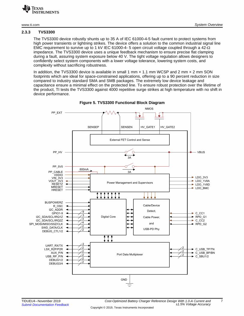
2.3.3 TVS3300The TVS3300 device robustly shunts up to 35 A of IEC 61000-4-5 fault current to protect systems fromhigh power transients or lightning strikes. The device offers a solution to the common industrial signal lineEMC requirement to survive up to 1 kV IEC 61000-4- 5 open circuit voltage coupled through a 42-Ωimpedance. The TVS3300 device uses a unique feedback mechanism to ensure precise flat clampingduring a fault, assuring system exposure below 40 V. The tight voltage regulation allows designers toconfidently select system components with a lower voltage tolerance, lowering system costs, andcomplexity without sacrificing robustness.
In addition, the TVS3300 device is available in small 1 mm × 1.1 mm WCSP and 2 mm × 2 mm SONfootprints which are ideal for space-constrained applications, offering up to a 90 percent reduction in sizecompared to industry standard SMA and SMB packages. The extremely low device leakage andcapacitance ensure a minimal effect on the protected line. To ensure robust protection over the lifetime ofthe product, TI tests the TVS3300 against 4000 repetitive surge strikes at high temperature with no shift indevice performance.
Figure 5. TVS3300 Functional Block Diagram
22 µF
+
±
22 µH
19 VDC
ControlLogic
+ ±
VREF
22 µF
TLV9001
TVS3300
TPS54202
0.596 V
FB
0.596 V
Ki = 59.6
Leakage Current
InputBias
Current
VBAT = 14 V
IBAT = 1 A
VIFB
Forward Current
Ku = 0.0355VIFB
System Overview www.ti.com
8 TIDUEU4–November 2019Submit Documentation Feedback
Copyright © 2019, Texas Instruments Incorporated
Cost-Optimized Battery Charger Reference Design With 1.0-A Current and±1.5% Voltage Accuracy
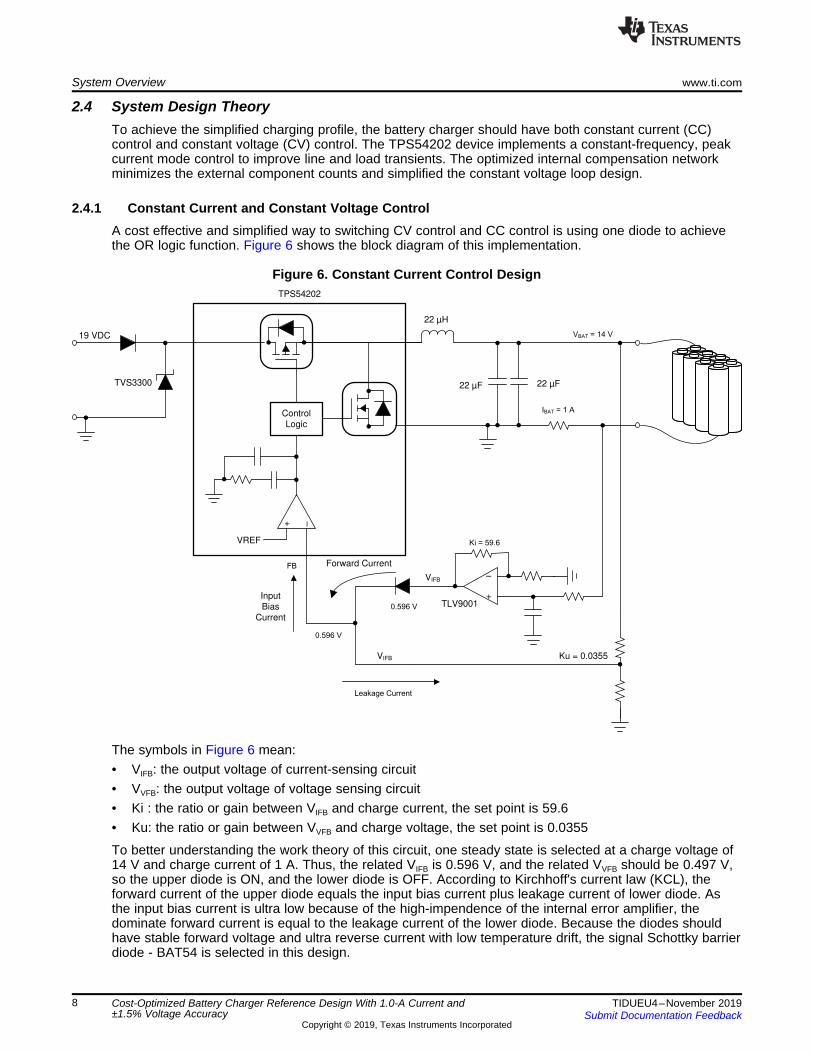
2.4 System Design TheoryTo achieve the simplified charging profile, the battery charger should have both constant current (CC)control and constant voltage (CV) control. The TPS54202 device implements a constant-frequency, peakcurrent mode control to improve line and load transients. The optimized internal compensation networkminimizes the external component counts and simplified the constant voltage loop design.
2.4.1 Constant Current and Constant Voltage ControlA cost effective and simplified way to switching CV control and CC control is using one diode to achievethe OR logic function. Figure 6 shows the block diagram of this implementation.
Figure 6. Constant Current Control Design
The symbols in Figure 6 mean:• VIFB: the output voltage of current-sensing circuit• VVFB: the output voltage of voltage sensing circuit• Ki : the ratio or gain between VIFB and charge current, the set point is 59.6• Ku: the ratio or gain between VVFB and charge voltage, the set point is 0.0355
To better understanding the work theory of this circuit, one steady state is selected at a charge voltage of14 V and charge current of 1 A. Thus, the related VIFB is 0.596 V, and the related VVFB should be 0.497 V,so the upper diode is ON, and the lower diode is OFF. According to Kirchhoff's current law (KCL), theforward current of the upper diode equals the input bias current plus leakage current of lower diode. Asthe input bias current is ultra low because of the high-impendence of the internal error amplifier, thedominate forward current is equal to the leakage current of the lower diode. Because the diodes shouldhave stable forward voltage and ultra reverse current with low temperature drift, the signal Schottky barrierdiode - BAT54 is selected in this design.
0.1
R5
GND
GND
I_BAT
GND DNPC32
0.1µF
C11
5
6
7B
TLV9002IDDFR
U3B
3.01k
R9
3.01k
R10
16.5kR11
ref fw
OUT out shunt
V VV I R
Gain
�
� u
www.ti.com System Overview
9TIDUEU4–November 2019Submit Documentation Feedback
Copyright © 2019, Texas Instruments Incorporated
Cost-Optimized Battery Charger Reference Design With 1.0-A Current and±1.5% Voltage Accuracy
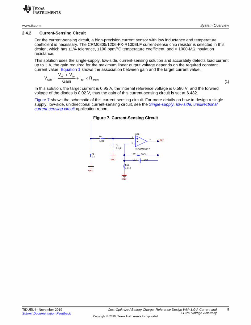
2.4.2 Current-Sensing CircuitFor the current-sensing circuit, a high-precision current sensor with low inductance and temperaturecoefficient is necessary. The CRM0805/1206-FX-R100ELF current-sense chip resistor is selected in thisdesign, which has ±1% tolerance, ±100 ppm/°C temperature coefficient, and > 1000-MΩ insulationresistance.
This solution uses the single-supply, low-side, current-sensing solution and accurately detects load currentup to 1 A, the gain required for the maximum linear output voltage depends on the required constantcurrent value. Equation 1 shows the association between gain and the target current value.
(1)
In this solution, the target current is 0.95 A, the internal reference voltage is 0.596 V, and the forwardvoltage of the diodes is 0.02 V, thus the gain of this current-sensing circuit is set at 6.482.
Figure 7 shows the schematic of this current-sensing circuit. For more details on how to design a single-supply, low-side, unidirectional current-sensing circuit, see the Single-supply, low-side, unidirectionalcurrent-sensing circuit application report.
Figure 7. Current-Sensing Circuit
Hardware, Software, Testing Requirements, and Test Results www.ti.com
10 TIDUEU4–November 2019Submit Documentation Feedback
Copyright © 2019, Texas Instruments Incorporated
Cost-Optimized Battery Charger Reference Design With 1.0-A Current and±1.5% Voltage Accuracy
3 Hardware, Software, Testing Requirements, and Test Results
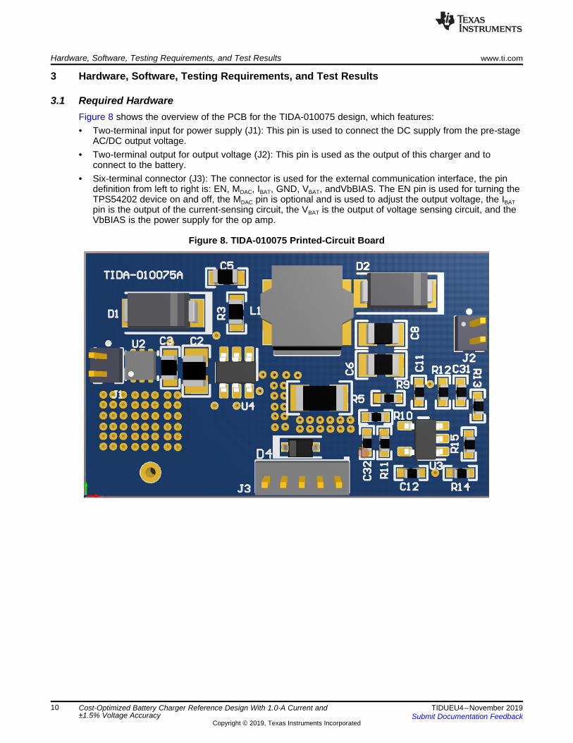
3.1 Required HardwareFigure 8 shows the overview of the PCB for the TIDA-010075 design, which features:• Two-terminal input for power supply (J1): This pin is used to connect the DC supply from the pre-stage
AC/DC output voltage.• Two-terminal output for output voltage (J2): This pin is used as the output of this charger and to
connect to the battery.• Six-terminal connector (J3): The connector is used for the external communication interface, the pin
definition from left to right is: EN, MDAC, IBAT, GND, VBAT, andVbBIAS. The EN pin is used for turning theTPS54202 device on and off, the MDAC pin is optional and is used to adjust the output voltage, the IBATpin is the output of the current-sensing circuit, the VBAT is the output of voltage sensing circuit, and theVbBIAS is the power supply for the op amp.
Figure 8. TIDA-010075 Printed-Circuit Board
www.ti.com Hardware, Software, Testing Requirements, and Test Results
11TIDUEU4–November 2019Submit Documentation Feedback
Copyright © 2019, Texas Instruments Incorporated
Cost-Optimized Battery Charger Reference Design With 1.0-A Current and±1.5% Voltage Accuracy
3.2 Testing and Results
3.2.1 Test Setup
Table 2. Test Environment List
MATERIALS USAGE COMMENTSDC Source Power Supply 30-V, 2-A Power sourceDC Source Power Supply 6-V, 1-A Power SourceTIDA-010075 Board Battery charger board ----Electronic Load Battery pack simulation CC, CV, CR modeComputer with PowerZ software Collect the charging data ----4S2P Li-Ion battery pack Load With protection circuit
The following steps show how to set up the test platform in the lab during the test:1. Ensure the TIDA-010075 board has the right output voltage at no load2. Connect the electronic load and choose the CV mode to test the constant output current3. Connect the electronic load and choose the CC mode to test the constant output voltage
Hardware, Software, Testing Requirements, and Test Results www.ti.com
12 TIDUEU4–November 2019Submit Documentation Feedback
Copyright © 2019, Texas Instruments Incorporated
Cost-Optimized Battery Charger Reference Design With 1.0-A Current and±1.5% Voltage Accuracy
3.2.2 Test Results
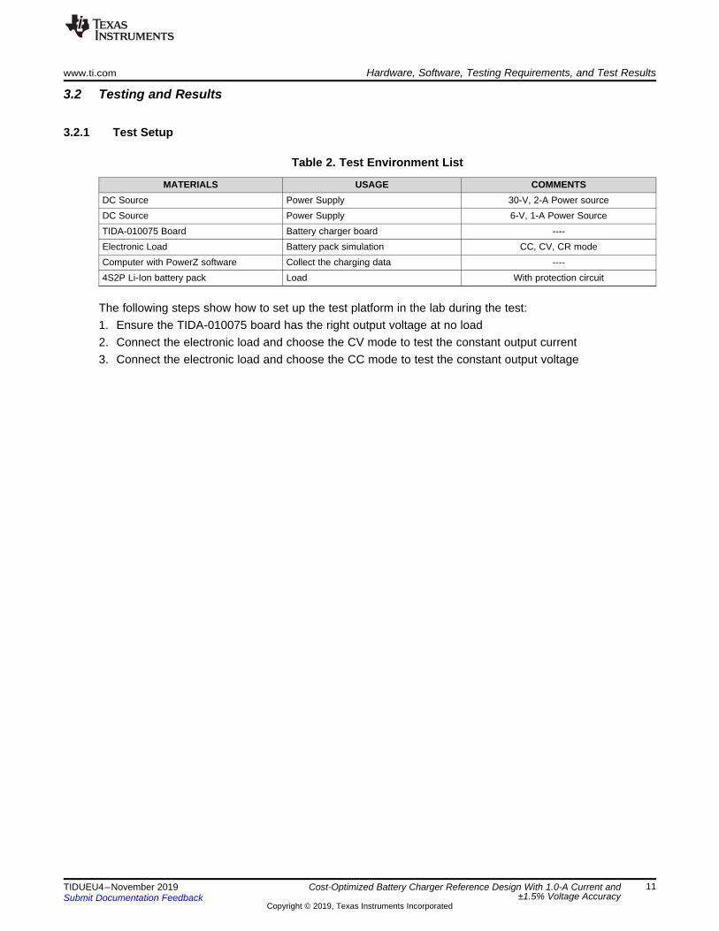
3.2.2.1 CV and CC Mode Steady StateFigure 9 shows the steady state of constant voltage (CV) mode and Figure 10 shows the steady state ofconstant current (CC) mode. The blue curve (CH2) is the output voltage and the purple curve (CH3) is theswitching frequency. The CV mode is tested at the following conditions: output voltage at 16.5 V and theoutput current at 0.5 A; the CC mode is tested at the following conditions: output voltage at 15 V andoutput current at 0.95 A.
Figure 9. CV Mode Steady State
Figure 10. CC Mode Steady State
www.ti.com Hardware, Software, Testing Requirements, and Test Results
13TIDUEU4–November 2019Submit Documentation Feedback
Copyright © 2019, Texas Instruments Incorporated
Cost-Optimized Battery Charger Reference Design With 1.0-A Current and±1.5% Voltage Accuracy
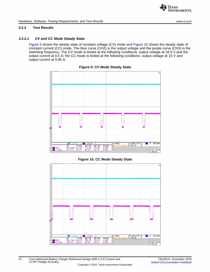
3.2.2.2 CV Voltage Ripple and CC Current RippleFigure 11 shows the voltage ripple of CV mode, and Figure 12 shows the current ripple of CC mode. Theoutput voltage ripple is less than ±3.8 mV, which also means the voltage accuracy is less than ±0.0023%.The output current ripple is tested by measuring the output voltage of the current-sensing circuit, thecurrent ripple is less than ±12 mA. which also means the current accuracy is less than ±1.2%.
Figure 11. CV Mode Voltage Ripple
Figure 12. CC Mode Current Ripple
Output Current (A)
Eff
icie
ncy (
%)
0.1 0.2 0.3 0.4 0.5 0.6 0.7 0.8 0.9 150
60
70
80
90
100
D001
Hardware, Software, Testing Requirements, and Test Results www.ti.com
14 TIDUEU4–November 2019Submit Documentation Feedback
Copyright © 2019, Texas Instruments Incorporated
Cost-Optimized Battery Charger Reference Design With 1.0-A Current and±1.5% Voltage Accuracy
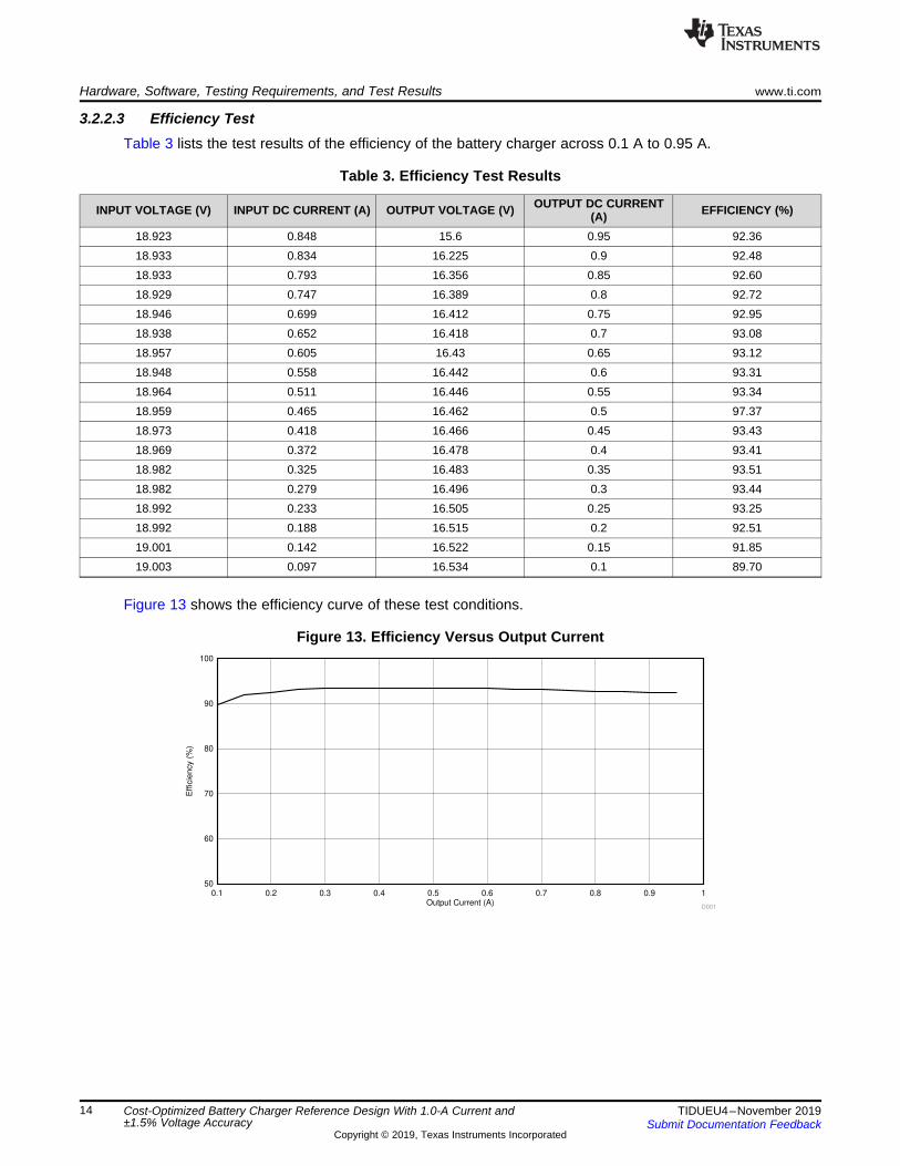
3.2.2.3 Efficiency TestTable 3 lists the test results of the efficiency of the battery charger across 0.1 A to 0.95 A.
Table 3. Efficiency Test Results
INPUT VOLTAGE (V) INPUT DC CURRENT (A) OUTPUT VOLTAGE (V) OUTPUT DC CURRENT(A) EFFICIENCY (%)
18.923 0.848 15.6 0.95 92.3618.933 0.834 16.225 0.9 92.4818.933 0.793 16.356 0.85 92.6018.929 0.747 16.389 0.8 92.7218.946 0.699 16.412 0.75 92.9518.938 0.652 16.418 0.7 93.0818.957 0.605 16.43 0.65 93.1218.948 0.558 16.442 0.6 93.3118.964 0.511 16.446 0.55 93.3418.959 0.465 16.462 0.5 97.3718.973 0.418 16.466 0.45 93.4318.969 0.372 16.478 0.4 93.4118.982 0.325 16.483 0.35 93.5118.982 0.279 16.496 0.3 93.4418.992 0.233 16.505 0.25 93.2518.992 0.188 16.515 0.2 92.5119.001 0.142 16.522 0.15 91.8519.003 0.097 16.534 0.1 89.70
Figure 13 shows the efficiency curve of these test conditions.
Figure 13. Efficiency Versus Output Current
www.ti.com Hardware, Software, Testing Requirements, and Test Results
15TIDUEU4–November 2019Submit Documentation Feedback
Copyright © 2019, Texas Instruments Incorporated
Cost-Optimized Battery Charger Reference Design With 1.0-A Current and±1.5% Voltage Accuracy
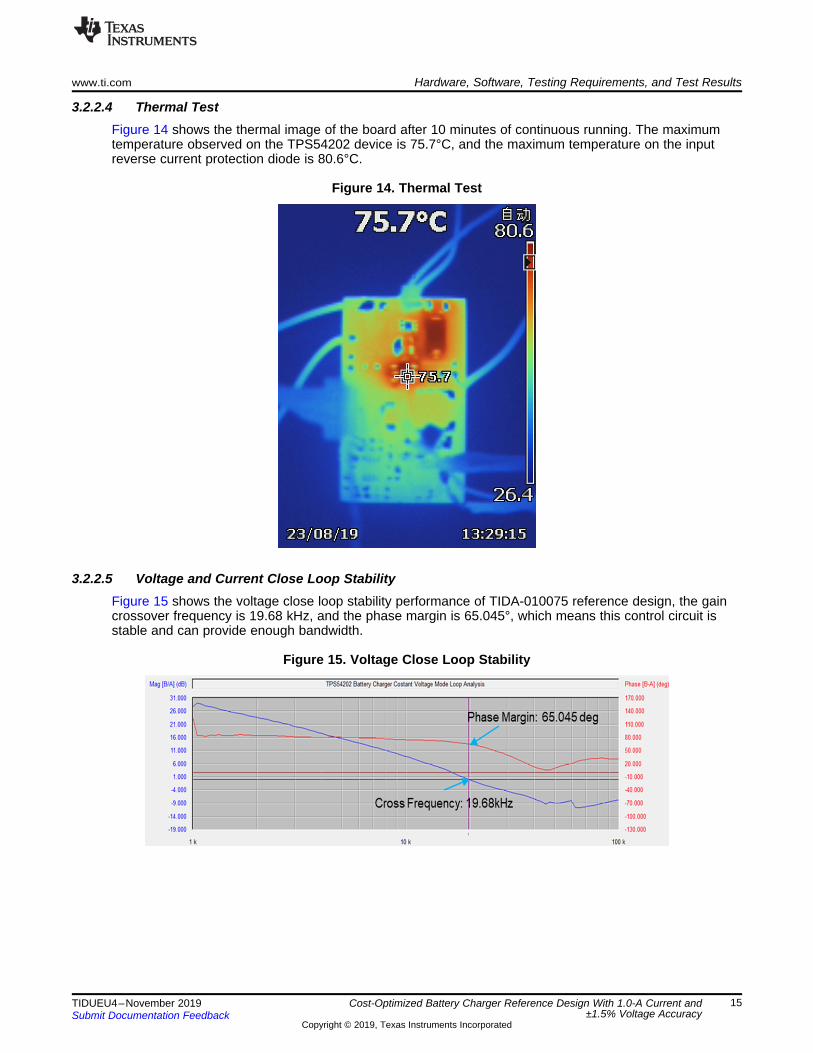
3.2.2.4 Thermal TestFigure 14 shows the thermal image of the board after 10 minutes of continuous running. The maximumtemperature observed on the TPS54202 device is 75.7°C, and the maximum temperature on the inputreverse current protection diode is 80.6°C.
Figure 14. Thermal Test
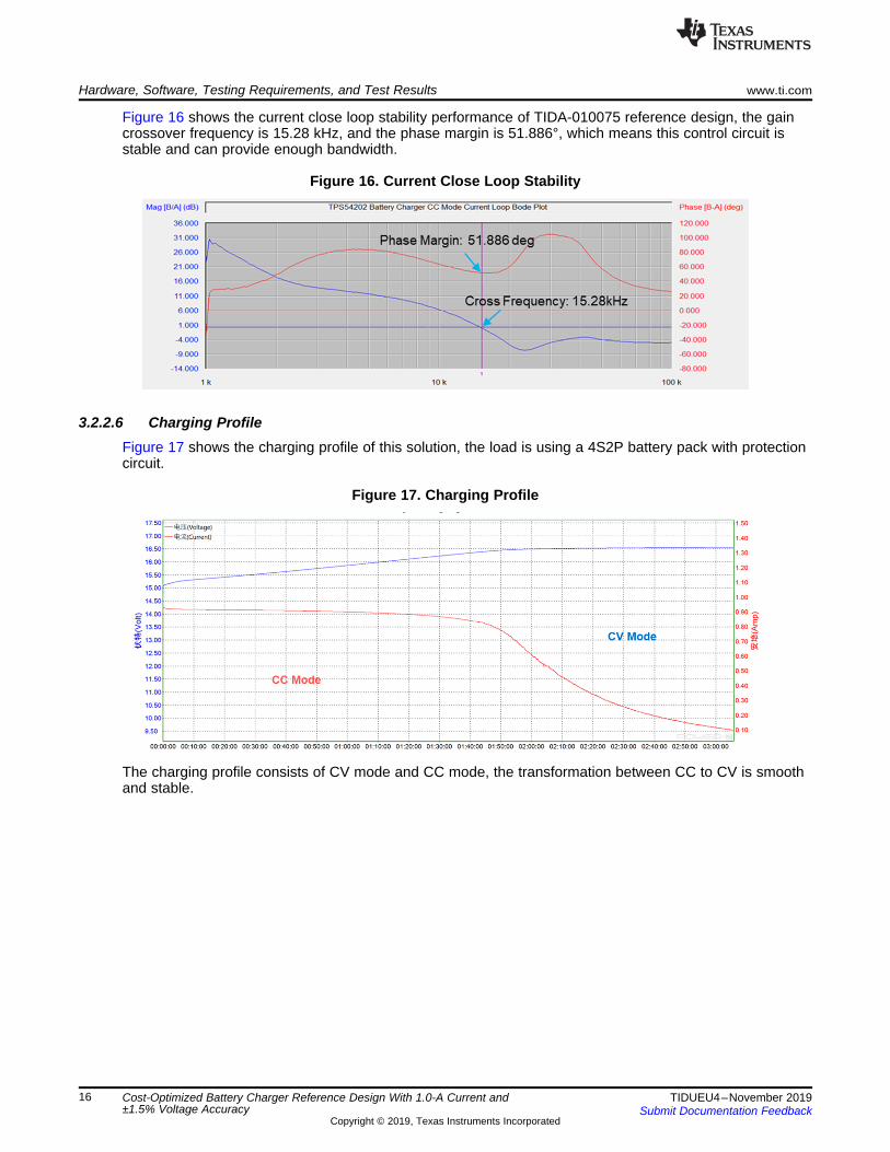
3.2.2.5 Voltage and Current Close Loop StabilityFigure 15 shows the voltage close loop stability performance of TIDA-010075 reference design, the gaincrossover frequency is 19.68 kHz, and the phase margin is 65.045°, which means this control circuit isstable and can provide enough bandwidth.
Figure 15. Voltage Close Loop Stability
Hardware, Software, Testing Requirements, and Test Results www.ti.com
16 TIDUEU4–November 2019Submit Documentation Feedback
Copyright © 2019, Texas Instruments Incorporated
Cost-Optimized Battery Charger Reference Design With 1.0-A Current and±1.5% Voltage Accuracy
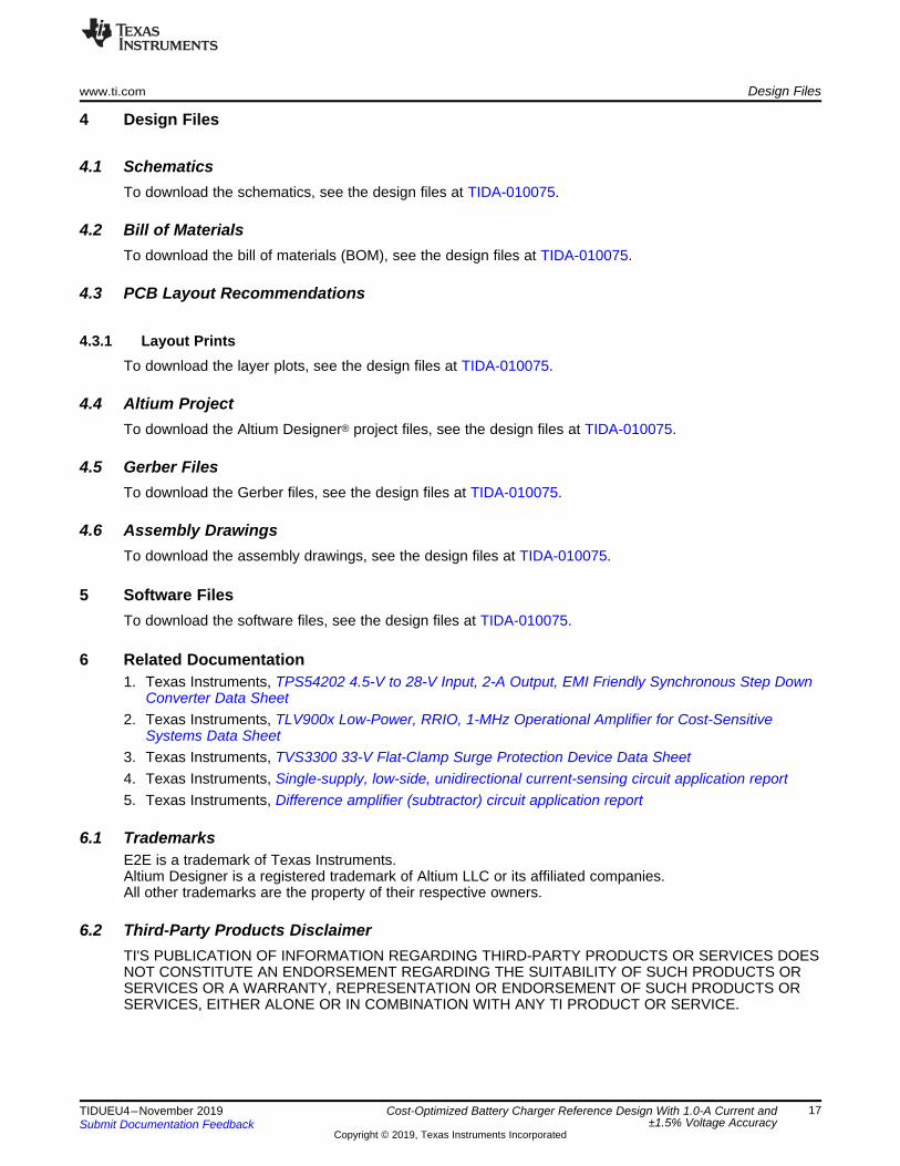
Figure 16 shows the current close loop stability performance of TIDA-010075 reference design, the gaincrossover frequency is 15.28 kHz, and the phase margin is 51.886°, which means this control circuit isstable and can provide enough bandwidth.
Figure 16. Current Close Loop Stability
3.2.2.6 Charging ProfileFigure 17 shows the charging profile of this solution, the load is using a 4S2P battery pack with protectioncircuit.
Figure 17. Charging Profile
The charging profile consists of CV mode and CC mode, the transformation between CC to CV is smoothand stable.
www.ti.com Design Files
17TIDUEU4–November 2019Submit Documentation Feedback
Copyright © 2019, Texas Instruments Incorporated
Cost-Optimized Battery Charger Reference Design With 1.0-A Current and±1.5% Voltage Accuracy
4 Design Files
4.1 SchematicsTo download the schematics, see the design files at TIDA-010075.
4.2 Bill of MaterialsTo download the bill of materials (BOM), see the design files at TIDA-010075.
4.3 PCB Layout Recommendations
4.3.1 Layout PrintsTo download the layer plots, see the design files at TIDA-010075.
4.4 Altium ProjectTo download the Altium Designer® project files, see the design files at TIDA-010075.
4.5 Gerber FilesTo download the Gerber files, see the design files at TIDA-010075.
4.6 Assembly DrawingsTo download the assembly drawings, see the design files at TIDA-010075.
5 Software FilesTo download the software files, see the design files at TIDA-010075.
6 Related Documentation1. Texas Instruments, TPS54202 4.5-V to 28-V Input, 2-A Output, EMI Friendly Synchronous Step Down
Converter Data Sheet2. Texas Instruments, TLV900x Low-Power, RRIO, 1-MHz Operational Amplifier for Cost-Sensitive
Systems Data Sheet3. Texas Instruments, TVS3300 33-V Flat-Clamp Surge Protection Device Data Sheet4. Texas Instruments, Single-supply, low-side, unidirectional current-sensing circuit application report5. Texas Instruments, Difference amplifier (subtractor) circuit application report
6.1 TrademarksE2E is a trademark of Texas Instruments.Altium Designer is a registered trademark of Altium LLC or its affiliated companies.All other trademarks are the property of their respective owners.
6.2 Third-Party Products DisclaimerTI'S PUBLICATION OF INFORMATION REGARDING THIRD-PARTY PRODUCTS OR SERVICES DOESNOT CONSTITUTE AN ENDORSEMENT REGARDING THE SUITABILITY OF SUCH PRODUCTS ORSERVICES OR A WARRANTY, REPRESENTATION OR ENDORSEMENT OF SUCH PRODUCTS ORSERVICES, EITHER ALONE OR IN COMBINATION WITH ANY TI PRODUCT OR SERVICE.
About the Author www.ti.com
18 TIDUEU4–November 2019Submit Documentation Feedback
Copyright © 2019, Texas Instruments Incorporated
Cost-Optimized Battery Charger Reference Design With 1.0-A Current and±1.5% Voltage Accuracy
7 About the AuthorZHILONG (BRYAN) LIU is a system engineer at Texas Instruments, responsible for developingsubsystem design solutions for the industrial appliances systems. He has system-level product experiencein analog and mixed-signal designs. Bryan earned his Bachelor of Technology in electrical and informationengineering from Xidian University, and his Master of Technology in circuit and system from XidianUniversity.

IMPORTANT NOTICE AND DISCLAIMER
TI PROVIDES TECHNICAL AND RELIABILITY DATA (INCLUDING DATASHEETS), DESIGN RESOURCES (INCLUDING REFERENCEDESIGNS), APPLICATION OR OTHER DESIGN ADVICE, WEB TOOLS, SAFETY INFORMATION, AND OTHER RESOURCES “AS IS”AND WITH ALL FAULTS, AND DISCLAIMS ALL WARRANTIES, EXPRESS AND IMPLIED, INCLUDING WITHOUT LIMITATION ANYIMPLIED WARRANTIES OF MERCHANTABILITY, FITNESS FOR A PARTICULAR PURPOSE OR NON-INFRINGEMENT OF THIRDPARTY INTELLECTUAL PROPERTY RIGHTS.These resources are intended for skilled developers designing with TI products. You are solely responsible for (1) selecting the appropriateTI products for your application, (2) designing, validating and testing your application, and (3) ensuring your application meets applicablestandards, and any other safety, security, or other requirements. These resources are subject to change without notice. TI grants youpermission to use these resources only for development of an application that uses the TI products described in the resource. Otherreproduction and display of these resources is prohibited. No license is granted to any other TI intellectual property right or to any thirdparty intellectual property right. TI disclaims responsibility for, and you will fully indemnify TI and its representatives against, any claims,damages, costs, losses, and liabilities arising out of your use of these resources.TI’s products are provided subject to TI’s Terms of Sale (www.ti.com/legal/termsofsale.html) or other applicable terms available either onti.com or provided in conjunction with such TI products. TI’s provision of these resources does not expand or otherwise alter TI’s applicablewarranties or warranty disclaimers for TI products.
Mailing Address: Texas Instruments, Post Office Box 655303, Dallas, Texas 75265Copyright © 2019, Texas Instruments Incorporated