titan g2 60-300 - microscop.ru · the titan™ g2 60-300 is the most powerful high resolution...
TRANSCRIPT

Product Data
Titan™ G2 60-300Deep sub-Ångström performance with the largest high tension range in S/TEM imaging and analysis optimized for a wide range of materials
NanoResearch strives to increase our understanding of nanostructures and functional
materials by linking the macroscopic material properties to the properties at the smallest
level of detail: down to atoms. This continuing drive pushes for the better understanding
of local atom organization and for the characterization of atoms, chemical bonding and
even the electronic structure. The Titan™ G2 60-300 is the most powerful high resolution
scanning transmission electron microscope (S/TEM) with the largest acceleration voltage
range of 60 to 300 kV for 2D and 3D material characterization and chemical analysis,
down to the atomic level, and delivers the ultimate performance in S/TEM imaging and
chemical analysis by allowing the option to combine Cs-correction, a monochromator, and
a novel available ultra-stable high brightness electron gun (X-FEG) in one instrument.
The Titan G2 60-300 with Cs-correction enables studies in STEM mode with a focused
probe or in TEM mode with a parallel beam with 80 pm guaranteed spatial resolution.
The system is based on the Titan platform technology which is unmatched in mechanical,
electronic, thermal, and optical stability and is designed to deliver the ultimate
performance in all TEM, STEM, energy fi ltered TEM (EFTEM), diff raction and electron
energy loss spectroscopy (EELS) & energy dispersive x-ray spectroscopy (EDS) modes. The
fl exibility of operating the Titan G2 60-300 in the range of 60 to 300 kV allows the
optimization of this important parameter to the requirements of the material examined,
from ultra-light carbon compounds to ultra-dense heavy metal materials. Additionally,
with the wide pole piece gap of the S-TWIN lens, the Titan G2 60-300 is designed for
dynamic experiments, which space to do more around the sample area.
An innovative modular and patented design makes a fi eld upgrade with a Cs-corrector
possible, allowing you a two-step approach to corrected microscopy in your laboratory.
The stability, performance and ease of use of Titan enables corrected microscopy to be
taken to the next level where new discoveries on the structure-property relationships of
materials become possible at ever-decreasing scales. Titan is poised to bring electron
microscopy into the new era by expanding the boundaries and achieving new results in
NanoResearch.
Key benefi ts•Increaseyourimagingandanalysiscapabilities
with CS-correctors and/or a monochromator •Maximizethequalityoftheresultsbychoosing
the optimum acceleration voltage (60 to 300 kV) to minimize artifacts and maximize contrast
•Increaseyourlateralresolutiontothe80pmlevelwith a large objective pole piece gap for ‘space to do more’
•Maximizetheinformationobtainedofyoursample in fi eld free imaging (< 2 Oe) with nanometer resolution on magnetic material
•Maximizetheflexibilityindiffraction(NBD,CBED,LACBED)withthenewcalibratedcondensersystem
•Maximizeyourcoherenceandbrightnessoftheelectron source with the unmatched performance of the ultra stable X-FEG electron gun
•Minimizingtheenergyspreadoftheelectronsource by adding a monochromator(< 0.2 eV) for HRTEM and with EELS spectroscopy applications
C09FI75_1 DS TiG2 60-300_E.indd 1 16-7-09 16:44

Product Data Titan™ G2 60-300
Page 2
Application results on Titan G2 60-300
Cs-corrected HR-STEM image on Ge112 at 300 kV with Fourier transformed showing 63 pm information transfer.
Cs-corrected HR-TEM image at 300 kV in Ge <110>.0.7 eV energy resolution (upper image).0.2 eV energy resolution (lower image).
Atomic resolution holography image (upper left) on gold grain boundary using an image Cs-corrector and an X-FEG. The Fourier transformed (upper right) shows sub-Ångström information transfer (arrows).
The reconstructed amplitude (left) and phase image (right) is shown below.Courtesy of Prof. M. Lehmann, M. Linck, Dr T. Niermann of TU Berlin, Germany, Prof. Hannes Lichte of TU Dresden, Germany, and Dr B. Freitag of FEI Company, The Netherlands.
Monochromized EELS spectrum on Si ,SiO2 , SiOxNy revealing the diff erent bonding states in the compounds.
Young’s fringe experiment on gold on carbon at 80/200 and 300 kV showing sub-Ångström information transfer.
AtomicresolutionEELSmappingonBaTiO3/SrTiO3interfaceacquiredusinga Probe Cs-corrector at 200 kV. Sample courtesy of C.L. Jia, Ernst Ruska Centre, Research Centre Juelich, Germany. Image data courtesy of Prof. Gianluigi Botton and Sorin Lazar, McMasters University, Canada.
Cs-corrected HR-TEM image on a fi lled SWCNT with fullerene structures on the surface of the SWCNT acquired at 60 kV acceleration voltage to minimize the beam damage. Sample courtesy of Prof. N. Kiselev, Institute of Crystallography, Moscow, Russia.
For detailed description see separate application note.
C09FI75_1 DS TiG2 60-300_E.indd 2 16-7-09 16:44

Product Data Titan™ G2 60-300
Page 3
Technical highlights•Optionalultra-stable,highbrightnessSchottkyfieldemittergun
(X-FEG, for more details see separate product data sheet)
•Newthreelenscondensersystemwithquantitativeindicationof
convergence angle and size of illuminated area for quantitative
measure of the electron dose and illumination conditions
•Flexiblehightensionfrom60to300kV(60,80,120,200,300kV)
•Onspecialrequest60kVCs-corrector alignments available
•ElectrongunmonochromatorforhighenergyresolutioninEELS
with symmetric energy distribution in zero-loss peak and improved
spatial resolution, especially at low kV HR-S/TEM
•CS-correction (probe and image CS-correction)
•80pmperformance
•Patentedmodularcolumndesignallowsaccuratemechanical
stacking system for low excitation of the deflector units in the
column to minimize instabilities due to electronic noise
•ConstantPower™lensdesignforultimatethermalstabilityinmode
and technique switches
•Lowhysteresisdesigntominimizecross-talkbetweenoptical
components
•SymmetricS-TWINobjectivelenswithwidepolepiecegapdesign
of 5.4 mm and ‘space to do more’ allowing the use of special
holders such as heating, cooling, dual-axis tomography and
STM/AFM holders
•Objectiveapertureinthebackfocalplaneoftheobjectivelensfor
optimum TEM dark field application work
•Readyforon-siteretrofitofaprobeorimageCS-corrector
•Automaticaperturesforremotecontroloperationandreproducible
recall of aperture positions during aperture change
•Rotation-freeimagingforeasyoperationandclearorientation
relationship between the image and diffraction plane
•Computerized5-axesspecimenstageforaccuratere-callofstored
positions, tracking of the areas visited during search for the right
area and ultra stable, deep sub-Ångström resolution with low
specimen drift
•Tiltrange±40degreesforanalyticaldoubletiltholdertoorientate
the maximum amount of zone axis of one crystal in polycrystalline
material.Withtomographyholdereven±80degreestominimize
the missing wedge in 3D reconstructions
•Field-freeimaging(<2Oe)inLorentzmodewith2nmresolution
for magnetic property studies
•OnspecialrequestCs-corrected field free imaging in Lorentz mode
with < 1 nm resolution for magnetic property studies
•TrueImage™focusseriessoftwareforquantitativeHR-TEM
applications (for more details see separate product data sheet)
•OnspecialrequesttheMultiLoaderisavailabletominimizethe
initial drift after sample loading and maximize your throughput
•Xplore3D™ software for automated tomography S/TEM
experiments and Xplore3D Xpress for ultra-fast 3D reconstructions
(for more details see separate product data sheet)
Detectors•HAADFdetector
•OnaxistripleDF1/DF2/BFdetectors
•GatanUS1000/US4000&Oriuscameras
•Eagleseriescameras
•Gatanenergyfilterseries
•Platecamera
•Si(Li)EDSdetectorwithsolidangleof0.13srad
and Fiori number > 4000
Titan G2 60-300 Energy spread Point resolution Information limit STEM resolution
Image corrector 0.7 to 0.8 eV** 80 pm 80 pm 136 pm
Probe corrector 0.7 to 0.8 eV** 200 pm < 100 pm 80 pm
Monochromator + X-FEG 0.2 to 0.3 eV* 200 pm 80 pm 136 pm
* Depending on energy filter option
** S-FEG 0.7 eV, X-FEG 0.8 eV
Note: All specifications are at 300 kV
For a list of specifications of other acceleration voltage please
contact your sales representative
C09FI75_1 DS TiG2 60-300_E.indd 3 16-7-09 16:44
World HeadquartersPhone: +1.503.726.7500
FEI EuropePhone: +31.40.23.56000
FEI JapanPhone: +81.3.3740.0970
FEI AsiaPhone: +65.6272.0050
See beyond at FEI.com
Product Data Titan™ G2 60-300
DS0056 07-2009© 2009. We are constantly improving the performance of our products, so all specifi cations are subject to change without notice. The FEI logo, Titan, ConstantPower, TrueImage and Xplore3D are trademarks of FEI Company, and FEI is a registered trademark of FEI Company. All other trademarks belong to their respective owners.
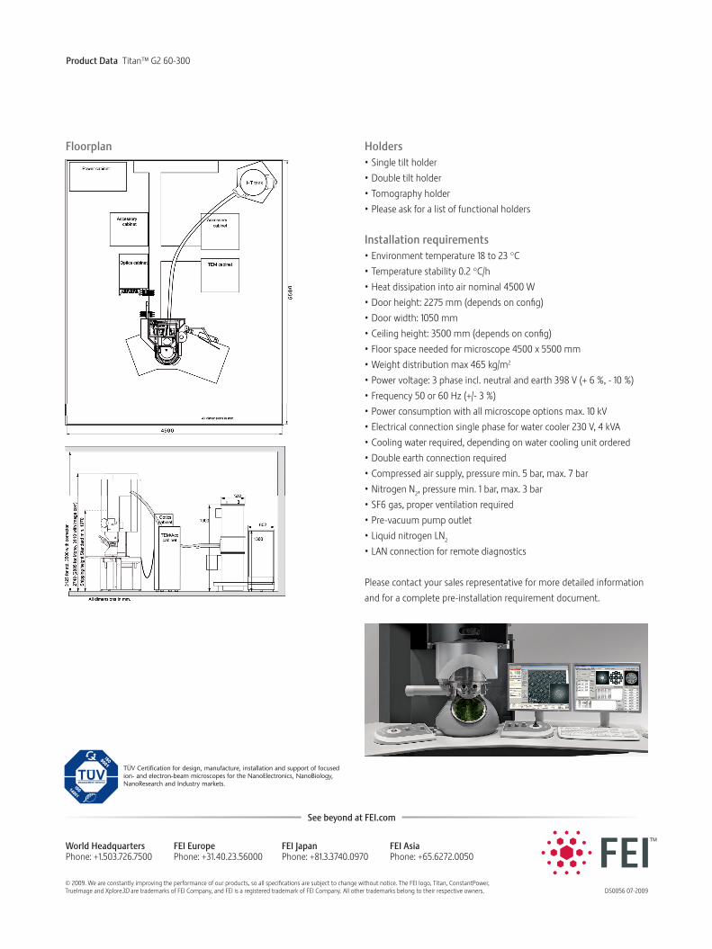
Floorplan Holders•Singletiltholder
•Doubletiltholder
•Tomographyholder
•Pleaseaskforalistoffunctionalholders
Installation requirements•Environmenttemperature18to23°C
•Temperaturestability0.2°C/h
•Heatdissipationintoairnominal4500W
•Doorheight:2275mm(dependsonconfig)
•Doorwidth:1050mm
•Ceilingheight:3500mm(dependsonconfig)
•Floorspaceneededformicroscope4500x5500mm
•Weightdistributionmax465kg/m2
•Powervoltage:3phaseincl.neutralandearth398V(+6%,-10%)
•Frequency50or60Hz(+/-3%)
•Powerconsumptionwithallmicroscopeoptionsmax.10kV
•Electricalconnectionsinglephaseforwatercooler230V,4kVA
•Coolingwaterrequired,dependingonwatercoolingunitordered
•Doubleearthconnectionrequired
•Compressedairsupply,pressuremin.5bar,max.7bar
•NitrogenN2, pressure min. 1 bar, max. 3 bar
•SF6gas,properventilationrequired
•Pre-vacuumpumpoutlet
•LiquidnitrogenLN2
•LANconnectionforremotediagnostics
Please contact your sales representative for more detailed information
and for a complete pre-installation requirement document.
TÜV Certification for design, manufacture, installation and support of focused ion- and electron-beam microscopes for the NanoElectronics, NanoBiology, NanoResearch and Industry markets.
C09FI75_1 DS TiG2 60-300_E.indd 4 16-7-09 16:44