title: class c tuned amplifier - sres · title: class c tuned amplifier ... practical diode...
TRANSCRIPT

Shree Ramachandra College of Engg., Pune 2015-16
Analog Communication Page1
Experiment No: 1 Date: / / 2016
Title: Class C Tuned Amplifier
AIM:Study of Class C Tuned amplifier. Design and test Class C tuned Amplifier at Centre frequency. PREREQUISITE: -Knowledge of C Amplifier, Tuned Amplifiers, etc.
OBJECTIVES:
APPARATUS:Class C Tuned amplifier kit, CRO, function generator, power supply.
THEORY:
Class C Amplifier Operation
In class C operation, collector current flows for less than one half cycle of the input signal. The class C
operation is achieved by reverse biasing the emitter-base junction, which sets the dc operating point below
cut-off and allows only the portion of the input signal that overcomes the reverse bias to cause collector
current flow. The class C operated amplifier is used as a radio-frequency amplifier in transmitters. From the
previous discussion, you can conclude that two primary items determine the class of operation of an
amplifier — (1) the amount of bias and (2) the amplitude of the input signal. With a given input signal and
bias level, you can change the operation of an amplifier from class A to class B just by removing forward
bias. Also, a class A amplifier can be changed to class AB by increasing the input signal amplitude. However,
if input signal amplitude is increased to the point that the transistor goes into saturation and cut-off, it is
then called an overdriven amplifier. You should be familiar with two terms used in conjunction with
amplifiers — fidelity and efficiency. Fidelity is the faithful reproduction of a signal. In other words, if the
output of an amplifier is just like the input except in amplitude, the amplifier has a high degree of fidelity.
The opposite of fidelity is a term we mentioned earlier distortion. Therefore, a circuit that has high fidelity
has low distortion. In conclusion, a class A amplifier has a high degree of fidelity. A class AB amplifier has
less fidelity, and class B and class C amplifiers have low or "poor" fidelity. The efficiency of an amplifier
refers to the ratio of output-signal power compared to the total input power. An amplifier has two input
power sources: one from the signal, and one from the power supply. Since every device takes power to
operate, an amplifier that operates for 360 degrees of the input signal uses more power than if operated
for 180 degrees of the input signal. By using more power, an amplifier has less power available for the
output signal; thus the efficiency of the amplifier is low.

Shree Ramachandra College of Engg., Pune 2015-16
Analog Communication Page2
APPLICATIONS:-
1. In RF transmitters-where the distortion can be vastly reduced by using tuned loads on the amplifier
stage.
PROCEDURE:
1. Connections are made as shown in the circuit diagram.
2. Adjust the input frequency of the signal to get the maximum output at the load.
3. For the applied DC voltage adjust the amplitude of sine wave signal so that the output signal peak to
peak amplitude is twice of the DC voltage(without any distortion)
4. Vary the load resistance RL around 10KW.
5. Note VO, VDC, IC and RL to find PAC and PDC hence the efficiency.
(Note: While measuring VO short the Ammeter connection)

Shree Ramachandra College of Engg., Pune 2015-16
Analog Communication Page3
IDEAL GRAPH:-
Observation table:-
f (Hz) Vo
(Volts)
VDC
(Volts)
IC
( mA)
RL
(Ohms)
PAC=Vo2/8RL
(mW)
PDC=VDCxIC
(mW) η =PAC/PDC
CONCLUSION:

Shree Ramachandra College of Engg., Pune 2015-16
Analog Communication Page4
Experiment No: 2-A Date: / / 2016
Title:AM Generation
AIM: AM Generation (DSB-FC): Calculation of modulation index by graphical method, Power of AM Wave for different modulating signal.
PREREQUISITE: -- Definition ofmodulation, modulation index & waveform of Amplitude Modulated wave.
EXPERIMENT OBJECTIVES:-
1. Observe the waveforms of modulating signal, carrier signal and amplitude modulated signal on CRO. 2. Calculate the Modulation Index by Envelope method.
APPARATUS:AM Wave Generation and Detection kit & CRO.
THEORY:
Information signals such as voice, video or binary data are sometimes transmitted directly from one point to
another over some communication medium. For example, voice signals are transmitted by way of wires in telephone
system. Coaxial cable carry video signals between two points and twisted cable is often used to carry binary data
from one point to another.
Modulation is the process of having the information to be communicated modifies a higher frequency signal called a
carrier. In Amplitude Modulation (AM), the amplitude of the carrier is changed in accordance with the amplitude and
frequency or the characteristics of the modulating signal. The carrier frequency remains constant. The amplitude
variation of the carrier peaks has the shape of the modulating signal and is referred to as the envelope. AM is
produced by a circuit called a modulator which has two inputs and an output. The modulator performs mathematical
multiplication of the carrier and information signals. The output is their analog product. The carrier in AM signal is a
sine wave that may be modulated by analog or digital information signals.
Need of Modulation:
Information signals cannot be radiated directly due to mainly two reasons:
The antenna length required for transmitting a wave is usually one quarter or one half of the length of the waves it is
set up to transmit. Then the length of the antenna will be many miles long which is impractical.Also, simultaneously
transmitted similar signals will interfere with each other since they occupy the same frequency range.Thus the
information signals modulate a high frequency signal called carrier. At higher frequencies, antenna sizes are much
smaller and signals propagate farther. There is also more room at higher frequencies. So many channels can be
formed to carry thousands of simultaneous communications without interference.
Modulation:
Definition: Modulation is the process of modifying the characteristic of one signal in accordance with the
characteristic of some other signal. The information signal is the modulating signal and the higher frequency signal
being modulated is called carrier signal.
Modulation Index (m): It is the ratio of modulating signal voltage to carrier signal voltage. This index is a number
between 0 and 1.When m<1, the condition is called under modulation, m=1 denotes complete modulation and m>1
shows over modulation.

Shree Ramachandra College of Engg., Pune 2015-16
Analog Communication Page5
CIRCUIT DIAGRAM:-

Shree Ramachandra College of Engg., Pune 2015-16
Analog Communication Page6
PROCEDURE: -
1) Make the connections as per the circuit diagram.
2) Check the connections.
3) Give 12V DC supply to the kit.
4) Give modulating signal of, 1 KHz to the MOD i/p terminal on the kit from the function
generator.
5) Give carrier signal of, 500 KHz to the carrier I/P terminal of the kit from the function
generator.
6) Observe the modulated o/p. Measure values of V max & V min & calculate the modulation index by
V max – V min
m = ____________ .
V max + V min
Verify it with the modulation index obtained in the previous step.

Shree Ramachandra College of Engg., Pune 2015-16
Analog Communication Page7
WAVEFORM:-
For m<1:
1. Draw the waveform for modulating signal showing amplitude and frequency. 2. Draw the waveform of carrier signal showing amplitude and frequency. 3. Draw the waveform of modulated output showing V max and V min. 4. Draw the trapezoidal patterns showing L1 and L2.
For m=1:
5. Draw the waveform for modulating signal showing amplitude and frequency. 6. Draw the waveform of carrier signal showing amplitude and frequency. 7. Draw the waveform of modulated output showing V max and V min. 8. Draw the trapezoidal patterns showing L1 and L2.
For m>1:
9. Draw the waveform for modulating signal showing amplitude and frequency. 10. Draw the waveform of carrier signal showing amplitude and frequency. 11. Draw the waveform of modulated output showing V max and V min. 12. Draw the trapezoidal patterns showing L1 and L2.
OBSERVATIONS:-
CONCLUSION:-
Sr. No. Em Ec m (%) Vmax Vmin m (%)
1
2
3

Shree Ramachandra College of Engg., Pune 2015-16
Analog Communication Page8
Experiment No: 2-B Date: / / 2016
Title:ENVELOPE DETECTOR
AIM: Envelope Detector - Practical diode detector, Observe effect of change in RC time constant Which leads to diagonal and negative clipping
PREREQUISITE: -1. Knowledge of amplitude modulation concept and working of basic diode detector circuit.
2. Concept of tuning, intermediate frequency and AGC.
, OBJECTIVES:1.To demodulate AM signal by practical diode detector circuit
2. To observe the effect of change in amplitude of modulating signal on the demodulated signal.
APPARATUS:AM Wave Generation and Detection kit & CRO, Power Supply, Function Generator.
THEORY:
When an amplitude modulated signal comes at the input of the detector circuit, it is first amplified using IF
amplifiers. This intermediate frequency is generated by a circuit called mixer. The mixer also receives signal from a
local oscillator. The output of the mixer is the input signal, the LO signal and their sum and difference frequencies.
This difference frequency is called Intermediate Frequency (IF). This amplified signal is fed to the detector. The
detector is the practical diode detector.
Operation of diode detector: The diode is by far the most common device used for AM demodulation (or detection),
and its operation will now be considered in detail. On the circuit of first figure, C is a small capacitance and R is a large
resistance. The parallel combination of R and C is the load resistance across which the rectified output voltage V0is
developed. At each positive peak of the RF cycle, C charges up to a potential almost equal to the peak signal voltage Va.
The difference is due to the diode drop since the forward resistance of the diode is small (but not zero). Between peaks a little
of the charge in C decays through R, to be replenished at the next positive peak. The result is the voltage V0, which
reproduces the modulating voltage accurately, except for the small amount of RF ripple. Note that the time constant of RC
combination must be slow enough to keep the RF ripple as small as possible, but sufficiently fast for the detector circuit to
follow the fastest modulation variations.
This simple diode detector has the disadvantages that V0, in addition to being proportional to the modulating voltage,
also has a dc component, which represents the average envelope amplitude (i.e., carrier strength), and a small RF ripple.
The unwanted components are removed in a practical detector, leaving only the intelligence and some second harmonic of
the modulating signal.
WAVEFORM:-
1. Modulating signal
2. Carrier signal
3 Modulated o/p of transmitter
4 Output signal of diode detector without filter
5. Output signal of diode detector with filter.

Shree Ramachandra College of Engg., Pune 2015-16
Analog Communication Page9
CIRCUIT DIAGRAM:-
Wc=Carrier Frequency
Wm=Maximam Signal Frequency
PROCEDURE:-
1. Make the connections of AM GENERATION KIT as per the circuit diagram.
2. Generate AM signal using AM Generator for modulating signal of 1 KHz and carrier signal 500 KHz.
3. Give this AM signal to the Demodulator kit.
4. Connect the output terminals to CRO.
5. Draw the waveform.( For two values of filter provided on the kit )
6. Change V m & Fm & repeat the same procedure.
CONCLUSION:-

Shree Ramachandra College of Engg., Pune 2015-16
Analog Communication Page10
Experiment No: 3 Date: / / 2016
TITLE:GENERATION OF DSB-SC
AIM: Generation of DSB-SC with the help of Balanced Modulator IC1496/1596 & its detection. PREREQUISITE: -Knowledge of DSB-S, Balance Modulator, product detector, RF Oscillator, etc.
APPARATUS:DSB-SC Generation kit, Spectrum Analyser, CRO.
THEORY:
The AM/DSB/SSB Modulation and Demodulation System consist of following sections.
1. Modulating Audio Signal Generator
2. Balanced Modulator Section
3. Product Detector Section
4. RF Oscillator Section
5. Band Pass Filter section
6. Detector Sections
7. Low pass Filter Section
8. Power supply Section
(1) Modulating Audio Signal Generator section:
IC 8038 - waveform generator - is used generate sine wave signal. 10K Pot is used to vary its
frequency. The frequency range is 300 Hz to 3.4Khz. Two 100K presets are adjusted for proper peaks of
sine wave signal. 1K preset is used to adjust duty cycle. The sine wave output signal available at pin 2 of IC
8038 is given to IC 356 through Amplitude pot for amplification. The amplified sine wave signal from pin 6
of IC 356 is then available at “SINE O/P”terminal. 22k Pot is used to vary the amplitude of Sine wave signal.
The output amplitude varies from 0 to 5Vpp.
(2) Balanced Modulator section:
IC 1496 is used as balanced modulator. The modulating audio signal is connected at pin 1 through buffer
transistor BC548B. This IC has two inputs as it works as balanced modulator. The Second input can be
connected at pin 4 through buffer transistor BC548B. The RF carrier signal is connected at pin 8 through
coupling capacitor from RF carrier oscillator section. The modulated outputs are available at pin 12 and 6
of this IC, which are then balanced amplified by transistor pairs -BC548B and BC558B. The final balanced
modulated output is available at AM MOD O/P terminal.100K preset is used to balance carrier signal while
1K preset is used to balance input audio signal. Output 1K preset is used to adjust output zero DC level.
Output 2K2 preset is used to vary level of AM modulated signal.

Shree Ramachandra College of Engg., Pune 2015-16
Analog Communication Page11
+1V signal is obtained from +15V DC supply by voltage divider consisting of 22K resistor and 4.7 K preset.
This +1 V is given to 2nd input of balanced modulator through +1VLink for AM modulation output to insert
carrier in AM output.
(3) Product detector circuit:
This section is similar to Balanced Modulator section. The difference is only that input pin 8 is given RF
carrier oscillator signal from RF carrier oscillator and pin 1 is given AM modulated signal from Balanced
Modulator section. The output is product of these two signals which contains basic audio modulating
signal, which can be filtered by low pass filter made of R-C (2K preset and 4n7 capacitor) circuit.
(4) R.F. Carrier Oscillator section:
1st BC548 Transistor is used generate RF sine wave signal. 15K Pot is used to vary its frequency. The frequency
range is 100 KHz to 1MHz. Then transistors pair BC558/BC548 and BC558/BC548) are used to amplify this RF
oscillation. The amplified RF sine wave signal available at emitter junction of BC558/BC548 is given to “RF O/P”
terminal through amplitude preset and Pot. There are two “RF O/P” signals. One is directly given to “RF CARRIER”
terminal of balanced modulator section. Second RF signal can be connected at “RF I/P” of Product detector
section.10K Pot is used to vary the amplitude of Sine wave signal. The output amplitude vary from 0 to 10Vpp.
(5) Band Pass Filter section: -
The filter made here is of Band pass filter having range 455 KHz to 458KHz. Crystal 455Khz is used as
Band pass filter. This filter is used to obtain Suppressed Carrier Double Side Band (DSB-SC) Modulated
signal from DSB signal.
(6). Detector Sections: -
(a) Diode detector circuit: -
This circuit consists of Diode OA79, two Capacitors C2 (22nf) and C1 (47nf) and Load resistor R. It works
as an envelope detector circuit. Resistor R –100K Pot and the capacitor C from a low pass filter meant to
reduce the carrier frequency ripple in the output. The values of R & C are chosen so as to remove even the
modulating signal frequency components. The magnitude of this dc voltage should vary as the carrier
amplitude in the input signal and should be independent of the depth of modulation and the modulating
signal frequency. C1, C2 can be selected through switch.
(b). Product detector circuit: -
This section is similar to Balanced Modulator section. The difference is only that input pin 8 is given RF

Shree Ramachandra College of Engg., Pune 2015-16
Analog Communication Page12
carrier oscillator signal from RF carrier oscillator and pin 1 is given AM modulated signal from Balanced
Modulator section. The output is product of these two signals which contains basic audio modulating
signal, which can be filtered by low pass filter made of R-C (2K preset and 4n7 capacitor) circuit.
(7). Low pass filter:
This section passes only low frequencies up to 3.4 KHz & reduces all other frequencies. This filter is
required to remove RF carrier signal components from demodulated signal. This section is based on IC 741
& R-C circuits
(8) Power supply section:
The regulated power supply is used for different supply voltages.
Following output D.C. Voltages are required to operate AM Modulation & demodulation system.
+15V, 250mA,
-15V, 250mA,
Three terminal regulators are used for different output voltages i.e. IC 7815 for +15V, IC 7915 for -
15V,These ICs are supplied different dc input voltages by two Bridge rectifiers consisting of D1-D4 and D5-
D8 & two 1000/25 EC and 1000/10 EC. The capacitors at each input & each output are for filtering purpose
BLOCK DIAGRAM OF DSB-SC AMPLITUDE MODULATION/DEMODULATION:-
Modulating Balanced modulator Audio Signal (without carrier insertion) Detected Output DSB-SC Amplitude
Modulated Signal
Audio Signal
RF Carrier
ModulatorDemodulator
Note: Remove 1+V RF Link in Balanced Modulator to suppress carrier in output.
Product
Detector
AF
RF

Shree Ramachandra College of Engg., Pune 2015-16
Analog Communication Page13
PROCEDURE:-
TO GENERATE DSB-SC AM SIGNAL:-
1. Connect following links:
a. Link between Sine O/P terminal of Audio Oscillator and MOD I/P terminal of balanced modulator.
2. Connect CRO channel-1 at Sine O/P terminal. Connect ground of probe to ground terminal of Audio
Generator. Adjust amplitude of sine wave to 1 Vpp and audio frequency to 1 KHz.---------------------Waveform (T1)
3. Connect CRO channel-2 at RF O/P terminal of RF Oscillator. Connect ground of probe to ground terminal
of Local oscillator. Adjust output frequency of RF oscillator to 455 KHz and amplitude to 10Vpp.---aveform (T2)
4. Now Connect CRO Channel 2 at AM MOD O/P terminal of balanced modulator. Trigger CRO by channel-1.
The DSB-SC Amplitude Modulated wave will be observed. -----------------------------------Waveform (T7)
5. See the effect on the DSB-SC AM modulated signal by varying the Audio Oscillator Frequency and a
amplitude.
6. Vary R.F. carrier Oscillator Frequency and Amplitude and observe its effect on the DSB-SC AM
To Demodulate Dsb-Sc Signal Using Product Detector: -
7. Now connect following links:
a. Modulated output of balanced modulator to the input of Product detector
i.e. Link between AM MOP O/P terminal of Balanced modulator and AM I/P of product detector.
b. Connect demodulator output signal of product detector to the input terminal of Low pass
Filter.i.e. Link between DEMO O/P terminal of product detector and I/P terminal of Low pass filter.
Connect CRO Channel 2 at filtered output terminal O/P in Low pass filter section.
Observe the demodulated sine wave signal. -------------------------------------------------------Waveform (T8)
9. Vary the Audio input Oscillator Frequency and Amplitude and see its effect on detected output signal.
10. Vary R.F. carrier Oscillator Frequency and Amplitude and observe its effect on the AM modulated signal.
11. Select diode polarity select switch to select upper or lower waveform for demodulation and observe its effect.
WAVEFORMS:-
TEST POINT WAVEFORMS – DSB-SC
T1. Modulating Sinewave signal: - (at Sine O/P terminal of Audio Oscillator) fm=1Khz, 1Vpp =
0.5V
-0.5V
1ms
H = 1 ms
V = 1 VPP
Trig = CRO-1

Shree Ramachandra College of Engg., Pune 2015-16
Analog Communication Page14
T2. R. F. Carrier Signal: - (at RF O/P terminal of RF Oscillator) fc = 455 KHz, 10Vpp
+5V
-5V 2.2us
T7. DSB-SC Modulated signal :- (at AM MOD O/P terminal of Product detector)
1/P +1.0V
fc -1.0V
1ms
T8. Demodulated DSB-SC Signal :- (at O/P terminal of Low pass filter)
+0.5V
-0.5V
CONCLUSION:
H = 1 ms
V = 1.0 VPP
Trig = CRO-2
H = 1us
V = 5.0 V
Trig = CRO-1
H = 1 ms
V = 1.0 VPP
Trig = CRO-2

Shree Ramachandra College of Engg., Pune 2015-16
Analog Communication Page15
Experiment No: 4 Date: / / 2016
Title: SSB Modulator
AIM: Study of SSB modulator using Filter method, phase shift method & its detection
APPARATUS: SSB modulator kit, Spectrum Analyser, CRO.
THEORY:
CIRCUIT DESCRIPTION OF SSB MODULATION & DEMODULATION
The AM/DSB/SSB Modulation and Demodulation System consist of following sections.
1. Modulating Audio Signal Generator
2. Balanced Modulator Section
3. Product Detector Section
4. RF Oscillator Section
5. Band Pass Filter section
6. Detector Sections
7. Low pass Filter Section
8. Power supply Section
(1) Modulating Audio Signal Generator section:
IC 8038 - waveform generator - is used generate sine wave signal. 10K Pot is used to vary its
frequency. The frequency range is 300 Hz to 3.4Khz. Two 100K presets are adjusted for proper peaks of
sine wave signal. 1K preset is used to adjust duty cycle. The sine wave output signal available at pin 2 of IC
8038 is given to IC 356 through Amplitude pot for amplification. The amplified sinewave signal from pin 6
of IC 356 is then available at “SINE O/P” terminal. 22k Pot is used to vary the amplitude of Sine wave
signal. The output amplitude varies from 0 to 5Vpp.
(2) Balanced Modulator section:
IC 1496 is used as balanced modulator. The modulating audio signal is connected at pin 1 through buffer
transistor BC548B. This IC has two inputs as it works as balanced modulator. The Second input can be
connected at pin 4 through buffer transistor BC548B. The RF carrier signal is connected at pin 8 through
coupling capacitor from RF carrier oscillator section. The modulated outputs are available at pin 12 and 6 of
this IC, which are then balanced amplified by transistor pairs -BC548B and BC558B. The final balanced
modulated output is available at AM MOD O/P terminal.100K preset is used to balance carrier signal while
1K preset is used to balance input audio signal. Output 1K preset is used to adjust output zero DC level.
Output 2K2 preset is used to vary level of AM modulated signal.+1V signal is obtained from +15V DC

Shree Ramachandra College of Engg., Pune 2015-16
Analog Communication Page16
supply by voltage divider consisting of 22K resistor and 4.7 K preset. This +1 V is given to 2nd input of
balanced modulator through +1V Link for AM modulation output to insert carrier in AM output.
(3). Product detector circuit:
This section is similar to Balanced Modulator section. The difference is only that input pin 8 is given RF
carrier oscillator signal from RF carrier oscillator and pin 1 is given AM modulated signal from Balanced
Modulator section. The output is product of these two signals which contains basic audio modulating signal,
which can be filtered by low pass filter made of R-C (2K preset and 4n7 capacitor) circuit.
(4) R.F. Carrier Oscillator section:
1st BC548 Transistor is used generate RF sine wave signal. 15K Pot is used to vary its frequency. The
frequency range is 100 KHz to 1MHz, transistor pair BC558/BC548 and BC558/BC548) are used to amplify
this RF oscillation. The amplified RF sine wave signal available at emitter junction of BC558/BC548 is
given to “RF O/P” terminal through amplitude preset and Pot. There are two “RF O/P” signals. One is
directly given to “RF CARRIER” terminal of balanced modulator section. Second RF signal can be
connected at “RF I/P” of Product detector section.10K Pot is used to vary the amplitude of Sine wave
signal. The output amplitude varies from 0 to 10Vpp.
(5) Band Pass Filter section: -
The filter made here is of Band pass filter having range 455 KHz to 458KHz. Crystal 455 KHz is used as
Band pass filter. This filter is used to obtain Suppressed Carrier Double Side Band (DSB-SC) Modulated
signal from DSB signal.
(6). Detector Sections: -
(a) Diode detector circuit: -
This circuit consists of Diode OA79, two Capacitors C2 (22nf) and C1 (47nf) and Load resistor R. It
works as an envelope detector circuit. Resistor R –100K Pot and the capacitor C from a low pass filter meant
to reduce the carrier frequency ripple in the output. The values of R & C are chosen so as to remove even the
modulating signal frequency components. The magnitude of this dc voltage should vary as the carrier
amplitude in the input signal and should be independent of the depth of modulation and the modulating
signal frequency. C1, C2 can be selected through switch.
(b). Product detector circuit: -
This section is similar to Balanced Modulator section. The difference is only that input pin 8 is given RF
carrier oscillator signal from RF carrier oscillator and pin 1 is given AM modulated signal from Balanced
Modulator section. The output is product of these two signals which contains basic audio modulating signal,
which can be filtered by low pass filter made of R-C (2K preset and 4n7 capacitor) circuit.

Shree Ramachandra College of Engg., Pune 2015-16
Analog Communication Page17
(7). Low pass filter:
This section passes only low frequencies up to 3.4 KHz & reduces all other frequencies. This filter is
required to remove RF carrier signal components from demodulated signal. This section is based on IC 741
& R-C circuits
(8) Power supply section:
The regulated power supply is used for different supply voltages.
Following output D.C. Voltages are required to operate AM Modulation demodulation system.
+15V, 250mA,
-15V, 250mA,
Three terminal regulators are used for different output voltages i.e. IC 7815 for +15V, IC 7915 for -
15V,These ICs are supplied different dc input voltages by two Bridge rectifiers consisting of D1-D4 and D5-
D8 & two 1000/25 EC and 1000/10 EC. The capacitors at each input & each output are for filtering purpose.
BLOCK DIAGRAM FOR SSB-SC AMPLITUDE MODULATION/DEMODULATION
Modulating Balanced
Audio Signal Modulator (without carrier insertion) Detected
Output
Audio Signal
RF Carrier
ModulatorDemodulator
Note: Remove 1+V RF Link in Balanced Modulator to suppress carrier in outpu t.
Product
Detector
AF
RF
Band pass
Filter

Shree Ramachandra College of Engg., Pune 2015-16
Analog Communication Page18
PROCEDURE:-
TO GENERATE SSB-SC AM SIGNAL:-
1. Connect following links:
a. Link between Sine O/P terminal of Audio Oscillator and MOD I/Pterminal of balanced modulator.
b. Link between RF O/P terminal of RF Oscillator and RF I/P terminal of Product detector.
2. Connect CRO channel-1 at Sine O/P terminal. Connect ground of probe to ground terminal
of Audio Generator. Adjust amplitude of sine wave to 1 Vpp and audio frequency to 3 KHz.
___ Waveform (T1)
3. Connect CRO channel-2 at DEMO O/P terminal product detector. Connect ground of probe
to ground terminal of Local oscillator
4. Adjust RF oscillator amplitude to 10 Vpp and frequency to 455 KHz.
___ Waveform (T2)
5. Connect the output of balanced modulator to the input of Band pass filter. i.e. connect link between
AM MOD O/P terminal of balanced modulator and INPUT terminal of Band Pass filter.
6. The output of Bandpass filter this filter is SSB -SC signal as it filters
455 KHz carrier signal. This waveform is similar to DSB-SC waveform on CRO in TIME DOMAIN
but it is different in
FREQUENCY DOMAIN and can be seen only on Spectrum Analyzer.
____Waveform (T9)
TO DEMODULATE SSB-SC SIGNAL USING PRODUCT DETECTOR: -
7. Connect output of Band pass filter to the input of Product detector. i.e. connect link between OUTPUT
terminal of Band Pass filter and AM I/P terminal of Product detector.
8. Connect demodulator output signal of product detector to the input terminal of Low pass filter.
i.e. Link between DEMOD O/P terminal of product detector and I/P terminal of Low pass filter.
8. Connect CRO Channel 2 at DEMOD O/P output terminal of product detector.

Shree Ramachandra College of Engg., Pune 2015-16
Analog Communication Page19
Start varying R.F. carrier frequency from 100 KHz to 460KHz. Carefully observe output on CRO.
10. The proper (maximum peak signal) demodulated sine wave will be available only at two carrier
frequencies.
This due to passing of Upper Side band and Lower side band at two different frequencies of RF carrier
frequencies.
______ Waveform (T10)
11. The theory for step 10 is as under.
(a) When AF frequency is 3 KHZ and RF frequency is 450 KHZ then
Output frequency of Product detector is
450+3 = 453 KHz - Upper Side Band
450-3 = 447 KHz - Lower Side Band
When these frequencies passes through band pass filter of bandwidth
452-458 KHZ, 453 KHz - Upper Side Band will pass and 447 KHz -
Lower Side Band will not pass. Hence one peak output will be
available at Upper Side band.
(b) When AF frequency is 3 KHZ and RF frequency is 458 KHZ then
Output frequency of Product detector is
458+3 = 461 KHz - Upper Side Band
458-3 = 455 KHz - Lower Side Band
When these frequencies passes through band pass filter of bandwidth 452-458 KHZ,
461 KHz - Upper Side Band will not pass and 455 KHz - Lower Side Band will pass.
Hence second peak output will be available at Lower Side band.
Thus proper (maximum peak signal) demodulated sine wave will be available only at two carrier
frequencies and it proves SSB-SC modulation.
WAVEFORMS:
TEST POINT WAVEFORMS – SSB-SC

Shree Ramachandra College of Engg., Pune 2015-16
Analog Communication Page20
T1. Modulating Sinewave signal: - (at Sine O/P terminal of Audio Oscillator) fm=3Khz, 1Vpp
+0.5V
-0.5V
0.33ms
T2. R. F. Carrier Signal: - (at RF O/P terminal of RF Oscillator) fc = 455 KHz, 10Vpp
+5V
-5V 2.2us
T9. SSB-SC Modulated signal :- (at AM MOD O/P terminal of Product detector)
+0.5V
-0.50V
0.33ms
Note that DSB-SC and SSB-Sc modulated waveform will look similar on CRO as CRO displays
time domain signals. Only on Spectrum Analyser both waveforms will differ.
H = 1 ms
V = 1 VPP
Trig = CRO-1
H = 1 ms
V = 1 VPP
Trig = CRO-2
H = 1us
V = 5.0 V
Trig = CRO-1

Shree Ramachandra College of Engg., Pune 2015-16
Analog Communication Page21
T10. Demodulated SSB-SC Signal: - (at DEMD O/P terminal of Product detector)
+2.0V
-2.0V
CONCLUSION: Thus we have studied generation of SSB-SC and its detectionusing Filter method, phase
shift method. This completes experiment of SSB-SC Amplitude modulation and demodulation.
H = 1 ms
V = 1 VPP
Trig = CRO-2

Shree Ramachandra College of Engg., Pune 2015-16
Analog Communication Page22
Experiment No: 5 Date: / / 2016
Title: AM Transmitter
AIM: Measure total power of the transmitterwith the help of Spectrum. Analyzer or Wattmeter, Observe
Variation in total power by varying modulation signal level.
PREREQUISITE: -Concept of AM Transmitter, Balance Modulator, product detector, RF Oscillator, etc.
APPARATUS:AM Transmitter kit & Spectrum Analyser, CRO, etc.
THEORY:
CIRCUIT DESCRIPTION OF AM TRANSMITTER
The AM transmitter consists of following sections.
9. Modulating Audio Signal Generator
10. Input Mike Amplifier Section
11. Balanced Modulator Section
12. RF Oscillator Section
13. Power amplifier
14. Power supply Section
(1) Modulating Audio Signal Generator section:
IC 8038 - waveform generator - is used generate sine wave signal. 10K Pot is used to vary its
frequency. The frequency range is 300 Hz to 3.4Khz. Two 100K presets are adjusted for proper peaks of sine wave
signal. 1K preset is used to adjust duty cycle. The sine wave output signal available at pin 2 of IC 8038 is given to IC
356 through Amplitude pot for amplification. The amplified sinewave signal from pin 6 of IC 356 is then available at
“Sine O/P”terminal. 22k Pot is used to vary the amplitude of Sine wave signal. The output amplitude varies from 0 to
5Vpp.
(2) Input Mike Amplifier section: -
The Input Audio amplifier circuit consists of one transistor BC 548B is connected in C-E configuration. The input
signal from mike is connected to the base of BC548 through coupling capacitor. The amplified audio signal obtained
at the collector of BC548 is given to transmitter section through volume control.
(3) Balanced Modulator section:
IC 1496 is used as balanced modulator. The modulating audio signal is connected at pin 1 through buffer transistor
BC548B. This IC has two inputs as it works as balanced modulator. The Second input can be connected at pin 4
through buffer transistor BC548B. The RF carrier signal is connected at pin 8 through coupling capacitor from RF
carrier oscillator section. The modulated outputs are available at pin 12 and 6 of this IC, which are then balanced
amplified by transistor pairs -BC548B and BC558B. The final balanced modulated output is available at AM MOD
O/P terminal.100K preset is used to balance carrier signal while 1K preset is used to balance input audio signal.
Output 1K preset is used to adjust output zero DC level. Output 2K2 preset is used to vary level of AM modulated
signal.+1V signal is obtained from +15V DC supply by voltage divider consisting of 22K resistor and 4.7 K preset.
This +1 V is given to 2nd input of balanced modulator through +1V Link for AM modulation output to insert carrier in
AM output.

Shree Ramachandra College of Engg., Pune 2015-16
Analog Communication Page23
(4) R.F. Carrier Oscillator section:
1st BC548 Transistor is used generate RF sine wave signal. 15K Pot is used to vary its frequency. The frequency
range is 100KHz to 1MHz. Then transistors pair BC558/BC548 and BC558/BC548) are used to amplify this RF
oscillation. The amplified RF sine wave signal available at emitter junction of BC558/BC548 is given to “RF O/P”
terminal through amplitude preset and Pot. There are two “RF O/P” signals. One is directly given to “RF CARRIER”
terminal of balanced modulator section. Second RF signal can be connected at “RF I/P” of Product detector
section.10K Pot is used to vary the amplitude of Sine wave signal. The output amplitude vary from 0 to 10Vpp.
(5). Output Power Amplifier section: -
The output amplifier circuit consists of two transistors BC 548B. 1st is connected as Emitter follower and 2nd is
connected as CE configuration. The gain controlled is provided between these stages. The output signal from balanced
modulator is connected to the base of 1st transistor and it is amplified. The amplified output is transmitted through
collector of second transistor and telescopic antenna.
(6) Power supply section:
The regulated power supply is used for different supply voltages.
Following output D.C. Voltages are required to operate AM transmitter system.
+15V, 250mA,
-15V, 250mA,
Three terminal regulators are used for different output voltages i.e. IC 7815 for +15V, IC 7915 for -15V.These
ICs are supplied different dc input voltages by two Bridge rectifiers consisting of D1-D4 and D5-D8 & two 1000/25
EC and 1000/10 EC. The capacitors at each input & each output are for filtering purpose.
BLOCK DIAGRAM

Shree Ramachandra College of Engg., Pune 2015-16
Analog Communication Page24
PROCEDURE:
1. Connect Output of Audio Generator to the MOD I/P terminal of balanced modulator.
2. Connect output of balanced modulator to the input of power amplifier. Adjust amplitude of sine wave to 1 Vpp
and audio Frequency to 1 KHz.
3. Connect CRO channel-1 at sine o/p terminal.Connect ground of probe to ground terminal of Audio Generator
4. Connect CRO channel-2 at RF O/P terminal of RF Oscillator. Connect ground of probe to ground terminal of
5. RF Oscillator. Adjust output frequency of RF oscillator to 1MHz and amplitude to 10 Vpp.
6. Now Connect CRO Channel 2 at AM MOD O/P terminal of balanced modulator.Trigger CRO by channel. The
Amplitude Modulated wave will be observed.
7. Keep AM radio receiver near transmitter and tune it to 1000 KHz and here 1 KHz tone.Measure collector
current IC and collector voltage VCE at T1 terminal of 2nd transistor of power amplifier. Calculate power by
formula P= VCE x IC in watts.
8. Now remove sine wave signal at input of modulator and connect output of mike amplifier. Connect condenser
mike and speak to mike. Here voice signal in AM receiver.
OBSERVATION TABLE:
fc=frequency of the carrier
EC =maximum amplitude of the carrier
AMPLITUDE FREQUENCY POWER IN dB
CARRIER EC fC
LSB mEC/2 fC-fm
USB mEC/2 fC+fm
CONCLUSION:

Shree Ramachandra College of Engg., Pune 2015-16
Analog Communication Page25
Experiment No: 6-A Date: / / 2016
Title: Frequency Modulator
AIM: Frequency modulator using varactor diode and NE 566 VCO, calculation of modulationindex.
PREREQUISITE: -Concept of FM generation, varactor diode, modulation index.
APPARATUS:FM generation kit, Spectrum Analyser, CRO, Function generator.
THEORY:
Frequency modulation is a system in which the amplitude of modulated carrier kept constant, while its frequency &
rate of change of frequency deviation are varied by modulating signal.There are different lower frequency VCO ,this
include IC, using RC multivibrator type oscillators whose frequency can be controlled over wide range by an AC or DC
i/p voltage. VCOs typically have an operating range of less than 1Hz to approx 1Mhz .
IC NE566 VCO is used for FM generation. The external resister R1 at pin no 6 sets the value of current set by the
internal current sources. The current sources linearly charge & discharge external capacitor at pin no 7.External
voltage VC applied at pin no 5 may also be used to vary current produce by the current sources. Schmitt-Trigger
circuit controls the current source by switching between charging & discharging of capacitor .The linear saw tooth
voltage developed across the capacitor by current source. This is buffered & made available at pin no 4.The Schmitt-
Trigger o/p is a square wave at the same frequency available at pin 3.
CIRCUIT DIAGRAM:-
PROCEDURE:-
1. Apply modulating signal to FM generator, using a function generator set frequency & amplitude .Observe
on D.S.O. & draw wave forms.
2. Set carrier frequency & amplitude observe & draw wave forms .Note down the frequency.
3. Set the type of modulation to FM.

Shree Ramachandra College of Engg., Pune 2015-16
Analog Communication Page26
4. Connect FM o/p to DSO & observe the wave forms. Draw it.
5. Remove modulating signal, observe &draw waveforms.
6. Increase amplitude of modulating signal &observe corresponding change in the O/P waveforms. Note
down f min & f max.
7. Connect modulating signal to CH2 of DSO. Compare amplitude of modulating signal &frequency of carrier.
8. Increase frequency of modulating signal &observe corresponding change in FM output. Note down f min
& f max.
OBSERVATION:-
CONCLUSION:
Sr .No. fm fmin fmax Δf
1
2
3
4

Shree Ramachandra College of Engg., Pune 2015-16
Analog Communication Page27
Experiment No:6-B Date: / / 2016
Title: Frequency Demodulator
AIM: FM demodulator using such as IC 565 (PLL based).
PREREQUISITE: -Concept of FM demodulator, PLL, VCO.
APPARATUS:FM generation & reception Kit., Spectrum Analyser, CRO, Function generator.
THEORY:
Phase Locked Loop (PLL) Demodulator: A PLL is a frequency or phase sensitive feedback control circuit. It is
used not only in frequency demodulation but also in frequency synthesizers. All PLLs have three basic elements. A
phase detector or mixer is used to compare the input or reference signal to the output of a VCO. The VCO frequency
is varied by the dc output voltage from a low pass filter. It is output of the phase detector that the low pass filter
uses to produce the dc control voltage.The primary job of the phase detector is to compare the two input signals and
generate an output signal that when filtered will control the VCO. If there is a phase or frequency difference
between the input and VCO signals, phase detector output will vary in proportion. The filtered output will adjust the
VCO frequency in an attempt to correct for the original frequency or phase change. This dc control voltage is called
the error signal and is also the feedback of the circuit.
To examine the operation of the PLL, assume initially that no input signal is applied. At this time the phase
detector and LPF outputs are zero. The VCO then operates at what is called its free running frequency. This is the
normal operating frequency of the VCO as determined by its internal frequency determining components.Now
assume that an input signal close to the frequency of the VCO is applied. The phase detector will compare the VCO
free running to the input frequency and produce an output voltage proportional to the frequency difference. The
resulting dc voltage is applied to the VCO. This dc voltage is such that it forces the VCO frequency to move in
direction that reduces the dc error voltage. The error voltage forces the VCO frequency to change in the direction
that reduces the amount of phase or frequency difference between the VCO and the input. At some point, the error
voltage will eventually cause the VCO frequency to equal the input frequency. When this happens, the PLL is said to
be in a locked condition.
Although the input and VCO frequencies are equal, there will be a phase difference between them that
produces the dc output voltage which causes the VCO to produce the frequency that will keep the circuit locked.
If the input frequency changes, the phase detector and LPF will produce a new value of dc control voltage that will
force the VCO output frequency to change until it is equal to the new input frequency. Because of this condition the
PLL is said to track the input signal. Any input frequency variation will be matched by a VCO frequency change so
that the circuit remains locked.
The VCO in a PLL therefore is capable of tracking the input frequency over a wide range. The range of
frequencies over which the PLL will track the input signal and remain locked is known as the lock range. The lock
range is usually a band of frequencies above and below the free running frequency of the VCO. If the input signal
frequency is out of the lock range, PLL will not lock. When this occurs, the VCO output frequency jumps to its free
Shree Ramachandra College of Engg., Pune 2015-16
Analog Communication Page28
running frequency. If an input signal within the lock range is applied to the PLL, the circuit will immediately adjust
itself and remain in a locked condition. The phase detector will determine the phase difference between the VCO
free running frequency and input frequencies and generate the error signal that will force the VCO to equal the input
frequency. Once the input signal is captured the PLL remains locked and will track any changes in the input signal as
long as it remains within the lock range.
The range of frequencies over which the PLL will capture an input signal is known as the capture range. It is
much narrower than the lock range, but it is generally centered around the free running frequency of the VCO as is
the lock range.The PLL is the best of all frequency demodulators in use. Its ability to provide frequency selectivity
and filtering give it a signal to noise ratio superior to any other type of FM detector. The linearity of VCO ensures a
highly accurate reproduction of the original modulating signal. Although PLLs are complex they are easy to apply
because they are available in low cost IC form.
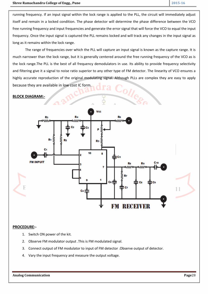
BLOCK DIAGRAM:-
PROCEDURE:-
1. Switch ON power of the kit.
2. Observe FM modulator output .This is FM modulated signal.
3. Connect output of FM modulator to input of FM detector .Observe output of detector.
4. Vary the input frequency and measure the output voltage.

Shree Ramachandra College of Engg., Pune 2015-16
Analog Communication Page29
CONCLUSION:-

Shree Ramachandra College of Engg., Pune 2015-16
Analog Communication Page30
Experiment No:7 Date: / / 2016
Title:FM Transmitter
AIM: Study of FM Transmitter; observe output waveform using Spectrum Analyzer and see the effect of
Eigen values on carrier power.
PREREQUISITE: -Concept of FMTransmitter, Spectrum Analyzer
APPARATUS:FM Transmitter kit & Spectrum Analyser.
THEORY:
Frequency modulation is the process or modulation in which frequency of the carrier is varied in accordance with the
instantaneous value of the modulating signal.
The AM transmitter consists of following sections.
15. Modulating Audio Signal Generator
16. Input Mike Amplifier Section
17. FM Oscillator and Mixer Section
18. Power supply Section
(1) Modulating Audio Signal Generator section:
IC 8038 - waveform generator - is used generate sine wave signal. 10K Pot is used to vary its
frequency. The frequency range is 300 Hz to 3.4Khz. Two 100K presets are adjusted for proper peaks of sine wave
signal. 1K preset is used to adjust duty cycle. The sine wave output signal available at pin 2 of IC 8038 is given to IC
356 through Amplitude pot for amplification. The amplified sine wave signal from pin 6 of IC 356 is then available at
“sine o/p”terminal. 22k Pot is used to vary the amplitude of Sine wave signal. The output amplitude varies from 0 to
5Vpp.
(2) Input Mike Amplifier section: -
The Input Audio amplifier circuit consists of one transistor BC 548B is connected in C-E configuration. The input
signal from mike is connected to the base of BC548 through coupling capacitor. The amplified audio signal obtained
at the collector of BC548 is given to transmitter section through volume control.
(3) FM oscillator and Mixer section:
This transistor Q2 (2n2369) works as mixer cum oscillator. R4 (10K) is base bias resistor for Q2. R6(470E) is load
resistor for Q2. C7 provides feedback to the emitter of Q2 for oscillations. C6 & L1 constitute Tank circuit load for Q2.
The transmission frequency can be varied by varying Gang capacitor C6. (350 Pf gang). The mixer output from
collector of Q2 is connected to antenna for transmission.
(4) Power supply section:
The regulated power supply is used for different supply voltages. Three terminal regulators are used for different
output voltages i.e. IC 7815 for +15V, IC 7915 for -15V,These ICs are supplied different dc input voltages by two
Bridge rectifiers consisting of D1-D4 and D5-D8 & two 1000/25 EC and 1000/10 EC. The capacitors at each input &
each output are for filtering purpose.

Shree Ramachandra College of Engg., Pune 2015-16
Analog Communication Page31
PROCEDURE:
7. Apply modulating signal to FM generator, using a function generator set frequency & amplitude .Observe on
D.S.O. & draw wave forms.
2. Set carrier frequency & amplitude observe & draw wave forms .Note down the frequency.
3. Set the type of modulation to FM.
4. Connect FM o/p to DSO & observe the wave forms.
5. Connect this FM output to Spectrum Analyser and check the frequency response.
CONCLUSION:

Shree Ramachandra College of Engg., Pune 2015-16
Analog Communication Page32
Experiment No: 8 Date: / / 2016
TITLE:CHARACTERISTICS OF RECEIVER
AIM:Measurement of Performance Characteristics of Receiver: Sensitivity, Selectivity, And Fidelity.
PREREQUISITE: -Concept of Frequency converter, Super heterodyne receiver.
APPARATUS:-Receiver kit, signal generator (AF/RF), Spectrum Analyser, CRO.
THEORY:
The Superhetrodyne circuit is used in almost all the transistor radios (except a few used for receiving local stations).
In this type of circuit the frequency of incoming signals is changed into a fixed frequency known as ‘intermediate
frequency IF’. The main work of amplifying the signal and of selecting the desired station, is done in IF section. This
permits higher amplification per stage and better selectivity.
The block diagram of a Radio receiver is shown in Fig.1. It consists of following parts/stages.
1. Frequency converter (Mixer and Oscillator)
2. I.F. amplifier
3. Detector
4. Audio preamplifier
5. Driver
6. Output
7. Power supply.
Figure-1
(1) Frequency converter :
It has two sections Mixer and Oscillator. Usually only one transistor is used for both sections. The Oscillator
produces oscillations at a frequency which is higher than the frequency of the station being received. The
difference equals the intermediate frequency (I.F.) Out of the signals intercepted by the aerial, the signals
from the desired stations are selected by a tuned circuit used at the input of the mixer stage. These signals
and the oscillations from the oscillator are mixed by the mixer. The mixing of these signals results in the
production of their sum (f1 + f2) and difference (f1 f2) frequencies. The difference is IF signal. It contains
the same modulation as contained by the received signals. The IF signals are then given to the IF amplifier.
Shree Ramachandra College of Engg., Pune 2015-16
Analog Communication Page33
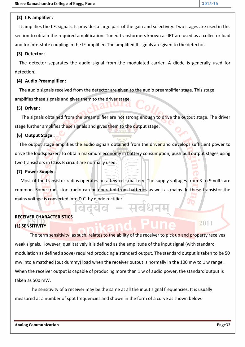
(2) I.F. amplifier :
It amplifies the I.F. signals. It provides a large part of the gain and selectivity. Two stages are used in this
section to obtain the required amplification. Tuned transformers known as IFT are used as a collector load
and for interstate coupling in the IF amplifier. The amplified If signals are given to the detector.
(3) Detector :
The detector separates the audio signal from the modulated carrier. A diode is generally used for
detection.
(4) Audio Preamplifier :
The audio signals received from the detector are given to the audio preamplifier stage. This stage
amplifies these signals and gives them to the driver stage.
(5) Driver :
The signals obtained from the preamplifier are not strong enough to drive the output stage. The driver
stage further amplifies these signals and gives them to the output stage.
(6) Output Stage :
The output stage amplifies the audio signals obtained from the driver and develops sufficient power to
drive the loudspeaker. To obtain maximum economy in battery consumption, push pull output stages using
two transistors in Class B circuit are normally used.
(7) Power Supply :
Most of the transistor radios operates on a few cells/battery. The supply voltages from 3 to 9 volts are
common. Some transistors radio can be operated from batteries as well as mains. In these transistor the
mains voltage is converted into D.C. by diode rectifier.
RECEIVER CHARACTERISTICS
(1) SENSITIVITY
The term sensitivity, as such, relates to the ability of the receiver to pick up and property receives
weak signals. However, qualitatively it is defined as the amplitude of the input signal (with standard
modulation as defined above) required producing a standard output. The standard output is taken to be 50
mw into a matched (but dummy) load when the receiver output is normally in the 100 mw to 1 w range.
When the receiver output is capable of producing more than 1 w of audio power, the standard output is
taken as 500 mW.
The sensitivity of a receiver may be the same at all the input signal frequencies. It is usually
measured at a number of spot frequencies and shown in the form of a curve as shown below.

Shree Ramachandra College of Engg., Pune 2015-16
Analog Communication Page34
(2) SELECTIVITY
The term selectivity refers to the ability of the receiver to select the signal to which it is tuned and
reject all other signals. Quantitatively, It is expressed in the form of a curve that shows the relative
amplitude of the required signal level to produce the standard test output as a function of the degree of
detuning. A typical curve is shown below.
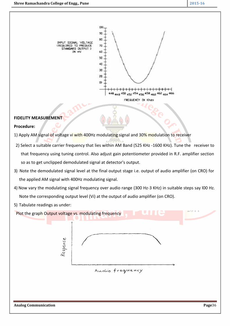
(3) FIDELITY
The fidelity refers to the overall response of the receiver to the modulating signal frequencies. It is
shown as the frequency response (output power in dB below the maximum power) when the input signal
level remains constant, the modulating signal frequency varies over the desired range and the depth of
modulation remind constant at 30 percent. A typical response is shown below
SENSITIVITY MEASUREMENT
Set up the equipments as shown in fig.. Replace the speakers by an output meter and set the
proper resistance on the meter. Set the receiver to the frequency at which the sensitivity is to be
determined.
DUMMY ANTENNA Audio Output
Procedure:
1) Apply AM signal of voltage with 400 Hz modulating signal and 30% modulation to
receiver.
2) Set the input carrier frequency so as to lie within the AM Band (525 KHz - 1600 KHz). Also tune the
detector to that carrier frequency using tuning control. (You will hear atone)
3) Set the input AM level. Also adjust the gain potentiometer provided on receiver so as to get
unclipped demodulated signal at detectors output.
4) Record input carrier frequency & signal level at the final output stage i.e. output of audio amplifier
(observed on CRO).
5) Change the input carrier frequency & also tune the receiver to that frequency & note down the
output voltage
6) Tabulate the collected readings as under:
7) Plot the graphH
AM GENERATION KIT
RADIO RECEIVER
CRO

Shree Ramachandra College of Engg., Pune 2015-16
Analog Communication Page35
SELECTIVITY MEASUREMENT
Procedure:
Ability of a radio receiver to reject unwanted signals is known as selectivity. Adjacent channel selectivity:
Ability of radio receiver to reject unwanted signal on the adjacent Channel (neighboring station) is known
as adjacent channel selectivity. To measure IF selectivity using IE-900A
1. Apply AM signal with 400 Hz modulating frequency and 30% modulation taken from AM generator kit to
AM receiver.
2. Set the input carrier frequency to suitable value that lies within the AM band (525 KHz - 1600 KHz). Also
set signal level to l00 mV.
3. Tune the Receiver using tuning control so as to get unclipped demodulated signal at detector's output
(output of audio amplifier).
4. Note the voltage level at receiver's final output stage i.e. audio amplifier's output on CRO (voltage at
resonance (Vr)).
5. Now gradually offset the carrier frequency in suitable steps of 5 KHz or 10 KHz below and above the
frequency adjusted in step 2 without changing the tuning of receiver & gain potentiometer.
6. Now record the signal level at output ofaudio amplifier for different input carrier frequency, on CRO (i.e.
voltage (Vi))
7. Tabulate the readings as under.
8. Plot the curve between output voltage vs carrier frequency.
Shree Ramachandra College of Engg., Pune 2015-16
Analog Communication Page36
FIDELITY MEASUREMENT
Procedure:
1) Apply AM signal of voltage vi with 400Hz modulating signal and 30% modulation to receiver
2) Select a suitable carrier frequency that lies within AM Band (525 KHz -1600 KHz). Tune the receiver to
that frequency using tuning control. Also adjust gain potentiometer provided in R.F. amplifier section
so as to get unclipped demodulated signal at detector's output.
3) Note the demodulated signal level at the final output stage i.e. output of audio amplifier (on CRO) for
the applied AM signal with 400Hz modulating signal.
4) Now vary the modulating signal frequency over audio range (300 Hz-3 KHz) in suitable steps say l00 Hz.
Note the corresponding output level (Vi) at the output of audio amplifier (on CRO).
5) Tabulate readings as under:
Plot the graph Output voltage vs. modulating frequency

Shree Ramachandra College of Engg., Pune 2015-16
Analog Communication Page37
OBSERVATION:
1) FOR SELECTIVITY
CARRIER FREQUENCY(Hz) O/P VOLTAGE Vi(V)
2) FOR SENSITIVITY
CARRIER FREQUENCY(Hz) O/P VOLTAGE Vi(V)
3) FOR FIDELITY
MODULATING FREQUENCY(Hz) O/P VOLTAGE Vi(V)
CONCLUSION:

Shree Ramachandra College of Engg., Pune 2015-16
Analog Communication Page38
Experiment No: 9 Date: / / 2016
TITLE: SAMPLING THEOREM
AIM:Verification of Sampling Theorem, PAM Techniques, (Flat top & Natural sampling), Effect of variable sampling rate, filter cutoff, reconstruction of original signal using Interpolation Filter. Aliasing Effect in frequency domain.
PREREQUISITE: -Concept of Sampling Theorem, PAM techniques, Aliasing.
APPARATUS:- Sampling & Reconstruction kit, CRO.
THEORY:
The sampling theorem circuit consists of following stages/sections.
1. Modulating Audio Signal Generator
2. Sampling Pulse Generator
3. Sampling section
4. Low pass filter demodulator section.
5. Power supply.
(1) Modulating Audio Signal Generator section: -
IC 8038- waveform generator IC is used generates sine wave signal. 10K Pot is used to vary its frequency. The
frequency range is 300 Hz to 3.4 KHz. Two 100K presets are adjusted for proper peaks of sine wave signal. 1K preset
is used to adjust duty cycle. The sine wave output signal is available at pin 2 of IC1 and it is then amplified by IC-356.
The amplified output is available Sine wave output terminal sine o/p. 22K Pot is used to Vary the amplitude of Sine
wave signal. The output amplitude varies from 0 to 5Vpp.
(2) Sampling Pulse Generator section: -
To obtain different types of sampling signals, Sampling pulse is required. This sampling signal is generated by
voltage-controlled oscillator (VCO) IC 4046. The pulse frequency is determined by varying control voltage of VCO at
pin 9 of this IC. This control voltage is varied by frequency pot (10K Pot).
The pulse width of this pulse signal is varied by using monostable IC 4528. The output of IC4046 is given to the +ve
trigger edge pin 4 of IC 4528. Then the pulse width of this signal is varied by this IC and output is available at pin 6.
The pulse width is varied by 100K pot. Thus sampling signal of variable frequency and pulse width is generated by
this section. The pulse frequency varies from 2 to 32 KHz.
(3) Sampling section (Modulator): -
To generate different types of sampling process, multiplexer IC 4053 is used as sample and Hold circuit. Two 741
ICs are used for input output impedance matching.
(a) Natural and Hold sampling: -
The modulating input signal is given to one input of IC 4053. The 10K resistor is connected at output of this IC by
connecting jumper J1. The sampling pulse is given to second input of this IC. The multiplexer output follows input
modulating signal during ON period (Sampling period). Then it becomes zero by resistor 10K. Then again it follows
input signal at ON time of next pulse. Thus natural sampled signal is generated.

Shree Ramachandra College of Engg., Pune 2015-16
Analog Communication Page39
(b) Sample and Hold sampling: -
The modulating input signal is given to one input of IC 4053. The capacitor 0.1/100 PPC is connected at output of
this IC by connecting jumper J1. The sampling pulse is given to second input of this IC. The capacitor is charged to the
current value of modulating signal by sampling pulse signal during ON period (Sampling period). Then this capacitor
holds this current voltage until next sample time comes. It slightly discharges during off period (Hold time). Then it
once again charges to the next value of modulating signal. Thus the voltage on this capacitor approximates to
modulating signal provided the modulating signal frequency is far less than sampling pulse frequency.
(c) Flat Top sampling: -
Here first sample and Hold (S/H) signal is generated as explained above. Then this signal is brought to zero level by
discharging capacitor 0.1/100PPC until next pulse arrives. This produces flat top sampled signal. To bring S/H signal
to zero, jumper J3 is connected. By connecting this jumper, the pulse width of sampling pulse is reduced which bring
output signal to zero until new pulse arrives.
(4) Demodulator section:
This section is based on low pass filter. It is based on two 741 IC and R-C circuits. It passes only low frequencies up
to 3.4 KHz and reduces all other frequencies. Thus it removes high frequency quantization noise of sampled signals
and original modulating signal is recovered.
(5) Power supply section:
The regulated power supply is used for different supply voltages. Three terminal regulators are used for different
output voltages i.e. IC 7805 for + 5V, IC 7815 for +15V, IC7915 for -15V,These ICs are supplied different dc input
voltages by two Bridge rectifiers consisting of D1-D4 and D5-D8 & two 1000/25 EC and 1000/10 EC. The capacitors at
each input & each output are for filtering purpose.
BLOCK DIAGRAM OF SAMPLING THEOREM
(1)NATURAL SAMPLING: -

Shree Ramachandra College of Engg., Pune 2015-16
Analog Communication Page40
(2) SAMPLE AND HOLD: -
PROCEDURE:-
A)TO GENERATE NATURAL SAMPLED PAM SIGNAL AND DEMODULATE IT:-
1. Connect DSO channel-1 at Sine O/P terminal. Connect ground of probe to ground terminal of Audio
oscillator. Adjust amplitude of sine wave to 2 Vpp and audio frequency to 1 KHz.
2. Connect sine wave O/P to input of Natural Sampling and connect clock pulse to control and connect control
o/p to signal clock of natural sampling.
3. Connect DSO Channel-1 at Natural sampling o/p of Modulator. The Natural sampled PAM signal will be
observed. Vary the frequency of the sine wave and observe its effect on PAM output.
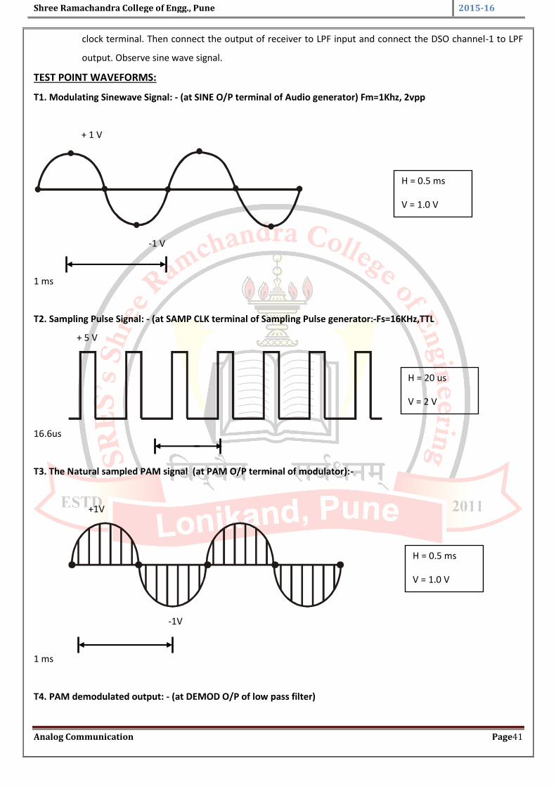
4. For demodulation connect natural sampling output to receiver input and connect control clock output to
clock terminal. Then connect the output of receiver to LPF input and connect the DSO channel-1 to LPF
output. Observe sine wave signal.
B) TO UNDERSTAND AND OBSERVE THE ALIASING EFFECT
5. Vary modulating sine wave frequency slowly. Observe the output atPAM O/P terminal. The slowly varying
waveform will be seen. This is known as “Aliasing effect”
C) TO GENERATE FLAT TOP PAM SIGNAL AND DEMODULATE IT:-
6. Connect sine wave O/P to input of Flat top Sampling and connect clock pulse to control and connect control
o/p to signal clock of Flat top sampling.
7. Connect DSO Channel-1 at Flat top sampling o/p of Modulator. The Fat top sampled PAM signal will be
observed. Vary the frequency of the sine wave and observe its effect on PAM output.
8. for demodulation connect Flat top sampling output to receiver input and connect control clock output to
Shree Ramachandra College of Engg., Pune 2015-16
Analog Communication Page41
clock terminal. Then connect the output of receiver to LPF input and connect the DSO channel-1 to LPF
output. Observe sine wave signal.
TEST POINT WAVEFORMS:
T1. Modulating Sinewave Signal: - (at SINE O/P terminal of Audio generator) Fm=1Khz, 2vpp
+ 1 V
-1 V
1 ms
T2. Sampling Pulse Signal: - (at SAMP CLK terminal of Sampling Pulse generator:-Fs=16KHz,TTL
+ 5 V
16.6us
T3. The Natural sampled PAM signal (at PAM O/P terminal of modulator):-
+1V
-1V
1 ms
T4. PAM demodulated output: - (at DEMOD O/P of low pass filter)
H = 0.5 ms
V = 1.0 V
Trig = CRO-1
H = 20 us
V = 2 V
Trig = CRO-2
H = 0.5 ms
V = 1.0 V
Trig = CRO-1

Shree Ramachandra College of Engg., Pune 2015-16
Analog Communication Page42
0.5V
1ms -0.5V
T5. The Sampled/Hold PAM signal (at PAM O/P terminal of modulator):-
+1V
-1V
1ms
CONCLUSION:
H = 0.5 ms
V = 0.5 V
Trig = CRO-1
H = 0.5 ms
V = 1.0 V
Trig = CRO-1

Shree Ramachandra College of Engg., Pune 2015-16
Analog Communication Page43
Experiment No: 9 Date: / / 2016
TITLE: AM Generation
AIM:Generate AM waveform for given modulation index, signal frequency and carrier frequency.
PREREQUISITE: -1. Knowledge of amplitude modulation concept and working of basic diode detector circuit.
2. Concept of tuning, intermediate frequency and AGC.
, OBJECTIVES: 1.To demodulate AM signal by practical diode detector circuit
2. To observe the effect of change in amplitude of modulating signal on the demodulated signal.
Software: MATLAB.
THEORY:
Amplitude modulation (AM) is a one of the conventional modulation technique to transmit signals using a carrier
wave. The amplitude or the strength of a high frequency carrier wave is changed in accordance with the amplitude
of message signal. First of all lets get into the basics..
Carrier signal (Sc) = Acsin(2πfct)
Message signal (Sm) = Amsin(2πfmt)
Where,
Ac – Amplitude of the carrier signal
Am – Amplitude of the message signal
fc – frequency of the carrier signal
fm – frequency of the message signal
When the signal is amplitude modulated, the amplitude of the high frequency carrier is varied in accordance with
the amplitude of message signal.
Modulated Signal = (Ac+ Amsin(2 πfmt))*sin(2 πfct)
Modulation Index or Modulation Depth is the one of the most common term that used along with modulation
techniques. Here in AM, it is the measure of amplitude variation surrounding an unmodulated carrier. It is the ratio
of the amplitude of message signal to the amplitude of carrier signal.
In terms of modulation index (m=Am/Ac) the equation of the modulated signal becomes,
Modulated signal = (1+ msin(2 πfmt))*Acsin(2 πfct)
Shree Ramachandra College of Engg., Pune 2015-16
Analog Communication Page44
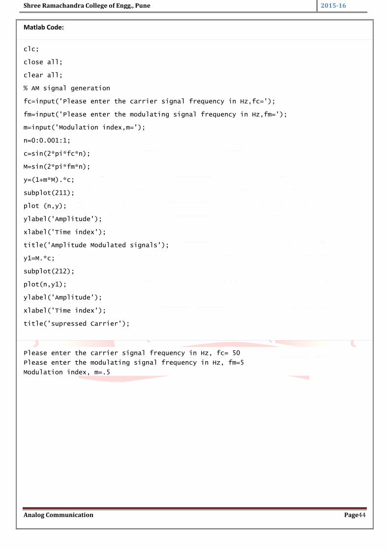
Matlab Code:
clc;
close all;
clear all;
% AM signal generation
fc=input('Please enter the carrier signal frequency in Hz,fc=');
fm=input('Please enter the modulating signal frequency in Hz,fm=');
m=input('Modulation index,m=');
n=0:0.001:1;
c=sin(2*pi*fc*n);
M=sin(2*pi*fm*n);
y=(1+m*M).*c;
subplot(211);
plot (n,y);
ylabel('Amplitude');
xlabel('Time index');
title('Amplitude Modulated signals');
y1=M.*c;
subplot(212);
plot(n,y1);
ylabel('Amplitude');
xlabel('Time index');
title('supressed Carrier');
Please enter the carrier signal frequency in Hz, fc= 50
Please enter the modulating signal frequency in Hz, fm=5
Modulation index, m=.5

Shree Ramachandra College of Engg., Pune 2015-16
Analog Communication Page45
Output Waveforms:
Conclusion:

Shree Ramachandra College of Engg., Pune 2015-16
Analog Communication Page46
Experiment No: 10 Date: / / 2016
TITLE: FM Generation
AIM:Generate FM waveform for given signal amplitude and carrier frequency.
PREREQUISITE: -Concept of FM generation, varactor diode, modulation index.
Software: -MATLAB.
THEORY:
Frequency modulation (FM) is the encoding of information in a carrier wave by varying the
instantaneous frequency of the wave. The amount of frequency variation is proportional to the Modulation index. A
major advantage of FM as compared with AM, is improved Signal-to-noise ratio (SNR). The improvement depends
on modulation level and deviation. For typical voice communications channels, improvements are typically 5-15 dB.
Matlab Code:
clc;
clear all;
close all;
fm=input('Message Frequency=');
fc=input('Carrier Frequency=');
mi=input('Modulation Index=');
t=0:0.0001:0.1;
m=sin(2*pi*fm*t);
subplot(3,1,1);
plot(t,m);
xlabel('Time');
ylabel('Amplitude');
title('Message Signal');
grid on;
c=sin(2*pi*fc*t);
subplot(3,1,2);
plot(t,c);
xlabel('Time');
ylabel('Amplitude');
title('Carrier Signal');
grid on;
y=sin(2*pi*fc*t+(mi.*sin(2*pi*fm*t)));%Frequency changing w.r.t Message
subplot(3,1,3);
plot(t,y);
xlabel('Time');
ylabel('Amplitude');
title('FM Signal');
grid on;

Shree Ramachandra College of Engg., Pune 2015-16
Analog Communication Page47
Output Waveforms:
Message Frequency=25
Carrier Frequency=400
Modulation Index=10
Conclusion: