title study on size effect of cluster ion beam irradiation
TRANSCRIPT
Title Study on Size Effect of Cluster Ion Beam Irradiation(Dissertation_全文 )
Author(s) Ichiki, Kazuya
Citation Kyoto University (京都大学)
Issue Date 2012-03-26
URL https://doi.org/10.14989/doctor.k16847
Right 許諾条件により要旨・本文は2012-09-01に公開
Type Thesis or Dissertation
Textversion author
Kyoto University

Study on Size Effect of Cluster Ion Beam
Irradiation
Kazuya Ichiki
February 2012


Abstract
A gas cluster is an aggregate of more than several hundred atoms. Each
constituent atom of a keV energetic gas cluster ion has thus only a few eV
of energy. When an energetic gas cluster ion strikes a target surface, each
constituent atom hits the local area at the same time and multiple-collision
processes occur. It was found that the irradiation effects induced by cluster
ion exceed by far the sum of all the individual irradiation effects of its
constituent atoms. Such so called “cluster size effects”, and many unique
phenomena such as high sputtering yield and surface smoothing under large
gas cluster ion beam (GCIB) bombardment have been observed. GCIB has
therefore recently been proposed to serve as a powerful tool for surface
smoothing, surface analysis and film formation.
In studies based on molecular dynamics simulation, we found that the
effects of irradiation with large cluster ions on defect formation and sputter-
ing depend on both the incident cluster size and energy of each constituent
atom (energy per atom), suggesting that the optimum irradiation conditions
for surface-smoothing with GCIB would differ from those for fast etching.
Nevertheless, in literature there are only a few experimental studies on the
relationship between incident cluster size and irradiation effects with large
GCIB. Indeed the usual distribution of sizes in the beam has a range of
more than several thousand atoms and therefore the irradiation effects of
a cluster of specific size cannot be measured experimentally without size
selection. In this work, we thus investigate the effects of cluster size and en-
ergy per atom on the interactions between GCIB and organic or inorganic
targets. The cluster size was selected with a time-of-flight method, which
permits effective cluster size selection, whether light(small) or heavy(large)
clusters are to be selected. The irradiation effects investigated were sput-
tering, secondary ion emission, surface damaging and surface roughening.
i

ii Abstract
Fundamentally, the amount of irradiation effects were found to decrease
monotonously with decreasing incident energy per atom, which the effect
of cluster size was relatively low. For example, the enhancement factor
of Si sputtering yield with GCIB was about 10 regardless of cluster size.
This is attributed to a saturation of the cluster size effects, the gas cluster
being sufficiently large abobe an initial threshold. The threshold energy
per atom for sputtering was found to depend on the incident cluster size
and the type of effect. The irradiation effects on organic and inorganic
targets were also found to be different, and this was mainly attributed to
the difference in target atoms binding energy and structures. In conclusion,
different irradiation effects could be specifically obtained by using size-
controlled GCIB. The use of GCIB in nanoprocesses such as no-damage
surface smoothing of inorganic materials or 3-dimensional secondary ion
mass spectrometry imaging of organic samples has thus been enabled by
size selection.

Acknowledgments
I would like to express my deep gratitude to Professor Akio Itoh and As-
sociate Professor Jiro Matsuo of Kyoto University for many helpful discus-
sions, their continuous guidance, encouragement throughout this study and
giving me the opportunity to complete this work.
I am very grateful to lecturer Toshio Seki and Takaaki Aoki for their
comments, scientific advice and helpful discussions in this study. I would
like to thank to Associate Professor Hiromi Shibata, Hidetsugu Tsuchida,
Assistant Professor Makoto Imai and Takuya Majima for valuable assis-
tance and stimulating comments. I also show my thanks to Chief in editor
of Edite Associate Rafael Manory for helpful comments in correcting and
improving the English in my papers. I wish to thank Ms. Masae Mogami
and Ms. Sachi Ibuki for their continuous cooperation and encourgement.
This research was made possible by the many cooperation and assistance
of many students and research fellows at Kyoto University. I would like to
thank to Mr. Syunnichiro Nakagawa, Mr. Yasuyuki Yamamoto and Mr.
Takahumi Yamanobe for analytical support and kind discussions. I also
show my thanks to Mr. Yoshinobu Wakamatsu, Mr. Yusaku Hontani and
Mr. Sho Shitomoto for sparing the time for discussion and continuous
encouragement in this work. I would like to express my thanks to Dr.
Matthieu Py for kind comments in my paper.
To Assistant Professor Satoshi Ninomiya of University of Yamanashi, I
would like to show my hearty thanks for significant discussion and experi-
mental advice. To Dr. Yoshihiko Nakata and Dr. Masaki Hada, I would like
to show deep gratitude for helpful discussions and many advices in solving
the problems. I wish to thank to Professor Hubert Gnaser of University of
Kaiserslautern for their helpful discussions.
Finally, I especially thank my parents and brothers for their continuous
iii

iv Acknowledgments
care, support and encouragement.

Contents
1 Introduction 1
1.1 What are clusters? . . . . . . . . . . . . . . . . . . . . . . . 1
1.2 Interaction between cluster ion and solids . . . . . . . . . . 2
1.3 GCIB applications for nano-processing . . . . . . . . . . . . 5
1.4 Purpose of this study . . . . . . . . . . . . . . . . . . . . . . 8
2 Sputtering yield with GCIB 11
2.1 Sputtering effects of ion beam bombardment . . . . . . . . 11
2.2 Size select GCIB irradiation . . . . . . . . . . . . . . . . . . 16
2.3 Results-Si target . . . . . . . . . . . . . . . . . . . . . . . . 23
2.4 Results-PMMA target . . . . . . . . . . . . . . . . . . . . . 32
3 Secondary ion emission with GCIB 39
3.1 Secondary ion mass spectrometry . . . . . . . . . . . . . . . 39
3.2 Size-selected cluster SIMS . . . . . . . . . . . . . . . . . . . 40
3.2.1 Time-of-flight mass spectrometry . . . . . . . . . . . 40
3.2.2 Size selected SIMS . . . . . . . . . . . . . . . . . . . 42
3.3 Results-Si target . . . . . . . . . . . . . . . . . . . . . . . . 46
3.3.1 Secondary cluster ion emission . . . . . . . . . . . . 46
3.3.2 Enhancement of Si+ emission . . . . . . . . . . . . . 51
3.4 Results-Organic materials . . . . . . . . . . . . . . . . . . . 57
4 Surface damage with GCIB 69
4.1 Low damage processing with GCIB irradiation . . . . . . . 69
4.2 Surface damage-Si target . . . . . . . . . . . . . . . . . . . 75
4.3 Surface damage-Organic materials . . . . . . . . . . . . . . 82
v

vi Contents
5 Surface morphology with GCIB 91
5.1 Surface smoothing with GCIB irradiation . . . . . . . . . . 91
5.2 Surface morphology-Si target . . . . . . . . . . . . . . . . . 92
5.3 Surface morphology-PMMA target . . . . . . . . . . . . . . 99
6 Summary and conclusions 107
7 Appendix 109
7.1 Energy loss during transportation . . . . . . . . . . . . . . . 109
References 119

Chapter 1
Introduction
1.1 What are clusters?
It is well known that the physical and chemical properties of matter change
from the isolated atom to bulk materials. For example, bulk mercury has
the properties of a metal; however, an isolated mercury atom does not
behave as metal anymore. The ‘cluster’ has been studied as the additional
phase that stands between the isolated atom and the bulk solid. The word
‘cluster’ means “a number of things that are grouped close together”, and
in this study these ‘things’ are atoms or molecules.
A cluster consists of more than two atoms or molecules that are bound
by various binding forces. The characteristics of a small cluster that con-
sists of a few atoms are similar to the isolated atom because all atoms are
at the surface of the cluster. On the other hand, the characteristic of large
clusters that consist of more than millions of atoms would be similar to the
bulk materials because only a small percent of atoms are at the surface. In
the case of band gap energy of mercury cluster, an insulator-to-metal tran-
sition occurs at an intermediate cluster size, which is about 400 atoms 1).
The understanding of clusters is by itself very important in fundamental
research, because clusters have a potential role in many fields of application
and technology.
Clusters can be roughly classified according to their binding force. Van
der Waals clusters, such as Arn and (O2)n are agglomerated by van der
Waals forces, and their binding energies are very weak (less than 0.1 eV).
Ionic clusters, such as (NaCl)n and Ir4(CO)12 are held together by ionic
1

2 Chapter 1. Introduction
bonding, and their binding energies are relatively strong (2 to 4 eV). Molec-
ular clusters, such as (I2)n are bound by dispersive electrostatic bonds,
and their bonding strength is between van der Waals and ionic bonding.
Hydrogen-bonded clusters, such as (H2O)n are associated by intermolecu-
lar H-bonding whose strength is as strong as molecular clusters. Valence
clusters, such as Cn and Sin are held together by covalent chemical bonds,
which are as strong as the ionic bonds. Metal clusters, such as Cun and
Aun are bound together by metallic or covalent bonds, and their binding
energies are in the range of a few eV. The properties of clusters are strongly
dependent on the type of bond and cluster size.
1.2 Interaction between cluster ion and solids
Not only the physical and chemical properties of the cluster itself, but the
interactions between energetic clusters and solids as well have attracted
much interest in the research community. When an energetic cluster bom-
bards the solid surface, clusters are broken up, and the constituents of
the cluster deposit the energy in the local area at the same time. Some
phenomena such as sputtering, are enhanced with energetic cluster bom-
bardment compared with energetic atom bombardment. In addition, some
unique phenomena, such as high chemical reactivity are achieved. There-
fore, cluster has been proposed as an ion beam source, and a vast quantity
of experimental data has been reported since the 1970’s. Figure 1.1 repre-
sents the typical clusters that have been used for ion beam sources. Their
size and structure is also shown.
The irradiation effect of cluster ion was first documented by Andersen
and Bay in 1974 by comparing dimers to monomers 2), and the irradiated
cluster ion was a metal cluster. Metal clusters are usually formed by laser
evaporation, field evaporation or inert gas condensation, and the size of the
cluster is up to about 15 atoms. Metal cluster formation was reported for
various metal atoms, and works on the irradiation effects of metal cluster
ion have accumulated since 1974. However, the quantity of metal clusters
produced decreases with cluster size and large metal clusters are difficult to
use. Metal cluster complexes are chemically synthesized from organometal-

1.2. Interaction between cluster ion and solids 3
Figure 1.1: The size and structure of typical clusters
lic compounds such as Ir4(CO)12 and Os3(CO)12, and they are larger than
typical metal clusters 3, 4). They consist of a metallic framework of several
metal atoms and surrounding ligands that are bound by covalent chemical
bonds. A metal cluster complex ion is relatively easy to produce to the
specific mass of a large cluster ion.
Fullerenes (C60) are one of the valence clusters and its soccer ball-like
structure is well known. C60 was discovered by Kroto and Smally in 1985 5)
as a new form of the element carbon, whose properties differ from those of
diamond or graphite. The study and application of C60 advanced in 1990’s
because of the discovery and development of a method of mass synthesis
by Kratschmer 6). The number of constituent atoms in C60 is much larger
than in metal clusters, but its mass (720 u) is roughly the same than small
metal clusters such as Au3 (591 u) and Bi3 (627 u).
Metal and carbon cluster ion beam presents however some problems.
For example, their constituents can be deposited on the surface if operated
under low-energy ion bombardment. Furthermore, the applicable cluster
size is small.
4 Chapter 1. Introduction
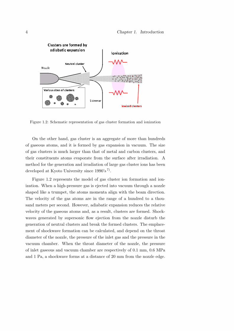
Clusters are formed by adiabatic expansion Ionization
Various sizes of clustersIonized clusters
Neutral clusterNozzle
SkimmerFigure 1.2: Schematic representation of gas cluster formation and ionization
On the other hand, gas cluster is an aggregate of more than hundreds
of gaseous atoms, and it is formed by gas expansion in vacuum. The size
of gas clusters is much larger than that of metal and carbon clusters, and
their constituents atoms evaporate from the surface after irradiation. A
method for the generation and irradiation of large gas cluster ions has been
developed at Kyoto University since 1990’s 7).
Figure 1.2 represents the model of gas cluster ion formation and ion-
ization. When a high-pressure gas is ejected into vacuum through a nozzle
shaped like a trumpet, the atoms momenta align with the beam direction.
The velocity of the gas atoms are in the range of a hundred to a thou-
sand meters per second. However, adiabatic expansion reduces the relative
velocity of the gaseous atoms and, as a result, clusters are formed. Shock-
waves generated by supersonic flow ejection from the nozzle disturb the
generation of neutral clusters and break the formed clusters. The emplace-
ment of shockwave formation can be calculated, and depend on the throat
diameter of the nozzle, the pressure of the inlet gas and the pressure in the
vacuum chamber. When the throat diameter of the nozzle, the pressure
of inlet gaseous and vacuum chamber are respectively of 0.1 mm, 0.6 MPa
and 1 Pa, a shockwave forms at a distance of 20 mm from the nozzle edge.

1.3. GCIB applications for nano-processing 5
To avoid the formation of such a shockwave, the skimmer is placed at the
center of the cluster beam flow and at about 20 mm from the nozzle edge.
Neutral clusters are introduced into the ionization chamber, and are ionized
by energized electrons emitted from a hot tungsten filament.
1.3 GCIB applications for nano-processing
When a gas cluster ion beam (GCIB) bombards a solid surface, thousands
of atoms strike the surface at the same time. The cluster energy is divided
to each constituent when cluster ion is broken up on the solid surface.
For example, a single constituent atom of 10 keV Ar1000 bears only 10
eV. Individual atomic ion bombardment with the energy of 10 eV hardly
penetrates the surface because the binding energy of inorganic atoms is
more than a few eV. However, 10 keV Ar1000 cluster penetrates a solid
surface such as silicon, and induces various irradiation effects, which are
fundamentally different from those associated with atomic or small cluster
ion impact. The characteristics of GCIB are enumerated below.
1. Low charge-to-mass ratio: an ionized gas cluster carries only single
or double charge, despite a cluster size of more than several hundred
atoms. Therefore, the space-charge repulsion of GCIB is small in
high-current ion beam transport, although the beam velocity is very
low. Because of this, GCIB can also avoid the charge-up effect during
ion beam irradiation.
2. Low-velocity bombardment: as mentioned, a typical gas cluster ion
has energy of a few tens eV/atom because the number of atoms in the
gas cluster is more than several hundreds. Consequently, the damaged
layer thickness under GCIB irradiation is very shallow compared to
atomic ion beam irradiation at comparable total energy. This char-
acteristic can be also applied to shallow implantation.
3. Strong chemical reaction: When an energetic GCIB bombards the
surface, the clusters transfer their energy to a very local and shallow
area on the solid surface. Surface atoms are excited by the GCIB

6 Chapter 1. Introduction
irradiation, resulting inan increase of the chemical reactions near the
surface with incident cluster species or atmospheric gas. Therefore,
the sputtering yield of a cluster ion of nonreactive gas is more than
one order of magnitude higher than that of atomic ions, and that of
a reactive GCIB is more than two orders of magnitude higher than
that of atomic ion at equal total energy.
4. Lateral migration effect: the CGIB impact deposits energy at high-
density on the surface, and numerous surface atoms are displaced.
Crater-like damage is formed by cluster ion. Under atomic bom-
bardment, the sputtered atoms are ejected with a cosine distribution.
On the other hand, GCIB bombardment induces lateral sputtering,
therefore reducing the surface grain and having a smoothing effect on
rough surfaces.
Because of their unique irradiation effects, GCIB processes can produce
unusual surface modification effects. Figure 1.3 shows GCIB applications
for nanoprocessing. High quality vanadium oxide films were obtained with
the O2-GCIB-assisted deposition technique 8) and fast and high-selectivity
etching of Si was performed with SF6-GCIB 9) thanks to the high chemical
reactivity of the beam. Because of the lateral migration effects, smoothing
of a rough diamond surface by Ar cluster ion beam was also possible re-
gardless of the target hardness 10). Formation of an ultra-shallow junction
was achieved by using B implantation through B10H14 GCIB 11).
In simulation and experiment, it was reported that incident cluster size
and energy are the important factors for large cluster irradiation effects.
The physics between the GCIB and the solid surface needs to be under-
stood in order to study the optimum gas cluster conditions for each pro-
cessing. The size of gas cluster can be controlled by adjusting the supply
gas and ionization conditions. For example, the mean cluster size increases
with increasing supply gas pressure (Ps) and decreasing ionization electron
voltage (Ve).
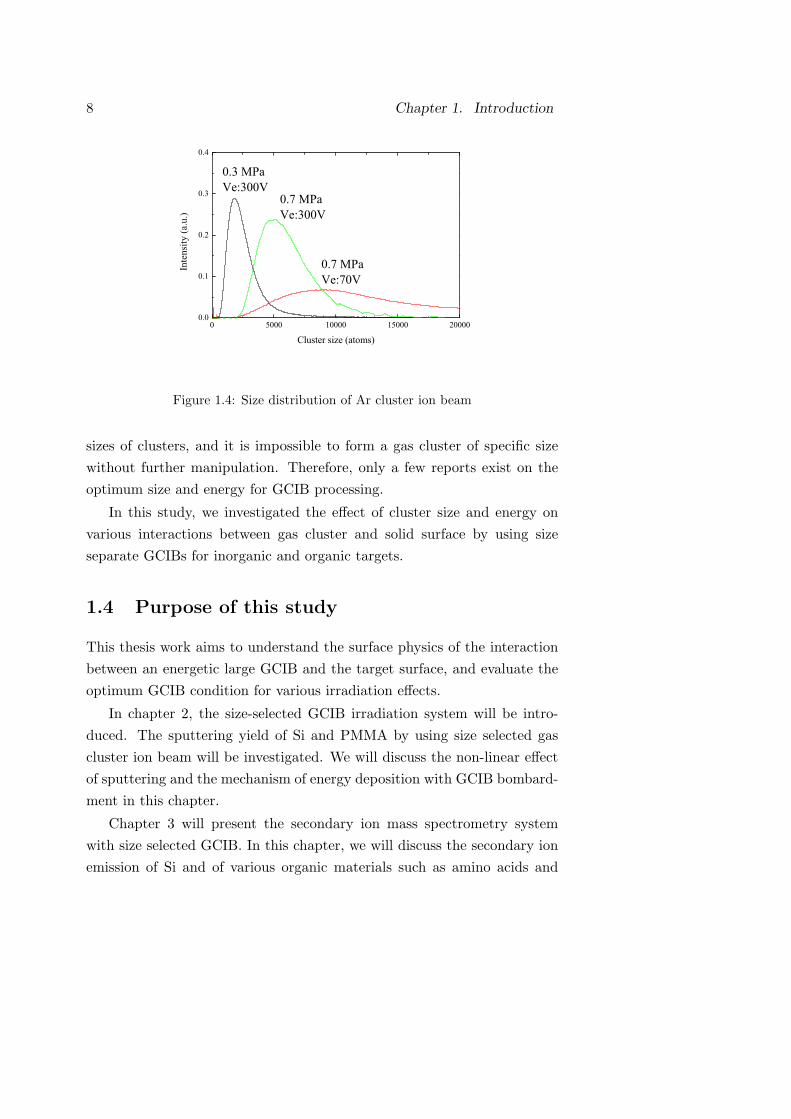
The size distributions of Ar cluster ion beam for different Ps and Ve
conditions are shown in Figure 1.4. The mean size of these cluster ions was
2000 and 7000 atoms, respectively. However, these beams contain various

1.3. GCIB applications for nano-processing 7
Film Formation
SEM images of thin film with O2cluster ion assisted deposition�Precise stoichiometry�High density�Smoothing surface
Surface smoothing
AFM images of diamond surface irradiated by Ar cluster ionAfter irradiation
Fast etching
SEM image of SiO2/Si substrateetched by SF6 cluster ion Before irradiation
Figure 1.3: GCIB applications for nano-processing
8 Chapter 1. Introduction
0 5000 10000 15000 200000.0
0.1
0.2
0.3
0.4
0.7 MPaVe:300V
0.7 MPaVe:70V
Inte
nsity
(a.u
.)
Cluster size (atoms)
0.3 MPaVe:300V
Figure 1.4: Size distribution of Ar cluster ion beam
sizes of clusters, and it is impossible to form a gas cluster of specific size
without further manipulation. Therefore, only a few reports exist on the
optimum size and energy for GCIB processing.
In this study, we investigated the effect of cluster size and energy on
various interactions between gas cluster and solid surface by using size
separate GCIBs for inorganic and organic targets.
1.4 Purpose of this study
This thesis work aims to understand the surface physics of the interaction
between an energetic large GCIB and the target surface, and evaluate the
optimum GCIB condition for various irradiation effects.
In chapter 2, the size-selected GCIB irradiation system will be intro-
duced. The sputtering yield of Si and PMMA by using size selected gas
cluster ion beam will be investigated. We will discuss the non-linear effect
of sputtering and the mechanism of energy deposition with GCIB bombard-
ment in this chapter.
Chapter 3 will present the secondary ion mass spectrometry system
with size selected GCIB. In this chapter, we will discuss the secondary ion
emission of Si and of various organic materials such as amino acids and
1.4. Purpose of this study 9
polymers. The secondary ion yield and intensity ratio of large secondary
ion will be investigated.
In chapter 4, the surface damage with GCIB bombardment will be inves-
tigated. In the search for the optimum cluster conditions for low damage
processing, the surface damage depth of a Si target and surface damage
accumulation of various organic materials will be discussed.
In chapter 5, we will discuss changes in the surface morphology of Si and
PMMA by GCIB bombardment. Surface smoothing is one of the important
irradiation effects of GCIB. The incident cluster condition effect on surface
roughnesswill be investigated in this chapter.
Finally, we will summarize the effect of incident cluster size and energy
per atom on surface irradiation effects, and the optimum conditions for
cluster irradiation in chapter 6.


Chapter 2
Sputtering yield with GCIB
2.1 Sputtering effects of ion beam bombardment
When a solid is bombarded by energetic ions, some atoms are ejected from
the surface and this process is known as “sputtering”. Typical energetic ions
with energy in the keV range penetrate the solid surface and their energy is
transferred to the solid atoms. In the case of Si, the calculated projection
range for 0 degree incidence of 10 keV Ar atomic ions is about 15 nm as
calculated with TRIM, indicating that the transferred energy is larger than
600 eV per nm 12). The atoms placed in the primary ion trajectory in the
solid collide elastically and recoil because their binding energies are only in
the order of a few eV. The recoiled atom continues to move and causes next
collisions with near atoms, and a cascade of atomic collisions occurs near
the solid surface. The sputtering phenomena take place when the recoiled
atoms produced at or near the surface have enough energy to eject from
the surface in an appropriate direction to escape the target.
Sputtering is one of the most important effects of ion beam irradiation,
and a large number of experimental and simulation results on sputtering by
energetic ions bombardment has been accumulated. The sputtering effect
with ion bombardment was first documented by J. J. Thomson in 1907,
and the physical process of sputtering was established by P. Sigmund etal.
in 1969 13). The energy transfer occurs in nuclear and electron interactions
between a primary ion and solid atoms. The energy is mainly transferred
via nuclear interactions in the energy range of below a few keV and by
electron interactions in the energy range larger than 1 MeV.
11
12 Chapter 2. Sputtering yield with GCIB
Under atomic ion bombardment in the keV energy range, the sputter-
ing yield is proportional to the nuclear stopping power of the target for
the energetic ions because the numbers of disordered atoms increase with
increasing transferred energy. Figure 2.1 (a) presents the model of target
atom displacement with atomic bombardment, under which target atoms
are energized and displaced by binary collision with incident ions, and the
sputtering yield with atomic ion bombardment can be calculated by the
linear collision cascade theory (Ylin)as follows.
Ylin(E) ∝ F (E)
U0(2.1)
where, E, F and U0 represent the incident energy, the deposited and
surface binding potential, respectively.
This theory insists on the sputtering yield being proportional to the
stopping power and inversely proportional to the surface binding energy.
The linear collision cascade theory has been the most successful in describ-
ing sputtering by keV atomic ion bombardment 14).
With Ar bombardment onto Si, sputtering occurs at an energy higher
than 40 eV. The sputtering yield of Si increases with increasing incident Ar
energy, and reaches the maximum value of about 2 atoms/ion at 10-50 keV
Ar irradiation.
When solids are bombarded with cluster ions, collision cascades are
induced by each constituent atom of the cluster and they overlap. The
density of recoil atoms and the density of energy deposited on the solid
surface by cluster ions is much higher than with atomic ions, and multiple
collisions take place between incident ions and target atoms. It was found
that the irradiation effects of cluster ions exceed the sum of the individ-
ual irradiation effects of constituent atom because of the multiple-collision
processes on the surface. For example, it was found that the sputtering
yield induced by a dimer hitting a surface was more than double that in-
duced by an atomic projectile at the same velocity. This enhancement of
sputtering yield is generally called “nonlinear effects” or “cluster effects”,
and has been observed experimentally since the 1970’s. Andersen and Bay
first reported 2) that the Ag sputtering yield by a Te dimer was about four

2.1. Sputtering effects of ion beam bombardment 13
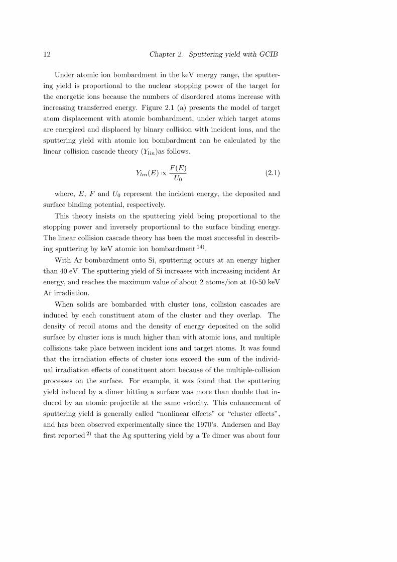
(a) (b)
Figure 2.1: Irradiation effect with (a)atomic and (b)cluster bombardment
times higher than that by a Te atom at the same velocity (200 keV/atom).
Bouneau etal. reported in 2002 that the nonlinear effect of Au sputtering
yield increased with increasing incident cluster size under small Au cluster
(≤ 13 atoms/ion) ion bombardment 15). The enhancement factor of Au13+
would be 20 to sputter an Au surface at the same velocity, indicating that
the Au sputtering yield by Au13+ was about 260 times higher than by Au+.
Figure 2.1 (b) represents the model of target atom displacement with
cluster bombardment. The sputtering yield is not in good agreement with
the linear collision cascade theory under cluster ion bombardment. As
long as the collision density is sufficient small, the energy deposition is
can be described by the linear Boltzmann transport equation because a
single binary collision occurred between the primary ion and the target
atom. The target atom has to be stable in the linear Boltzmann transport
theory when the collision occurs, however target atoms are no longer stable
under high density energy deposition with cluster ion bombardment. The
cascade evolves resulting in the formation of a highly disrupted, very hot
region inside the solid. This region where this takes place is called a thermal
spike.
A model of the sputtering yield with thermal spike, Yth, was described
by Sigmund and Claussen in 1981 16) as:
14 Chapter 2. Sputtering yield with GCIB
Yth(E) ∝ F (E)2
U20
(2.2)
Ylin is proportional to the deposited energy, whereas Yth varies propor-
tional to the square of deposited energy.
Monte-Carlo (MC) simulations are used to calculate the collision pro-
cess of atomic ions in a solid. The MC simulation method which is based
on the binary collision theory made it possible to examine the evolution
of collision cascades, formation of damage and sputtering with atomic ion
bombardment. However, this method is not suitable for analyzing the clus-
ter impact process because of the multiple collisions between incident ion
and surface atoms.
Instead of the MC simulation method, the method of molecular dy-
namics (MD) simulation has been developed for describing cluster-solid
interactions since the 1990’s. In MD simulation, the motion of all atoms
involved in the collision process is described, and the Newton’s equation of
motion is solved numerically for all atoms in the system within steps of the
order of femtoseconds to picoseconds, which permit in-situ-, real time-like
observation.
The concept of the MD method is very simple, but it requires quite
larger memory resources and longer computational times than the MC
method based on binary collision theory. Because of improvements in com-
puters and low-cost availability, theoretical research through MD simula-
tion is now the normal approach for understanding the complexity of the
interactions in a collision which is more difficult to be solved analytically.
Nonlinear effects between cluster ion and target were first calculated by
MD simulations by Shapiro etal. in 1989 17) and Shugla etal. in 1990 18).
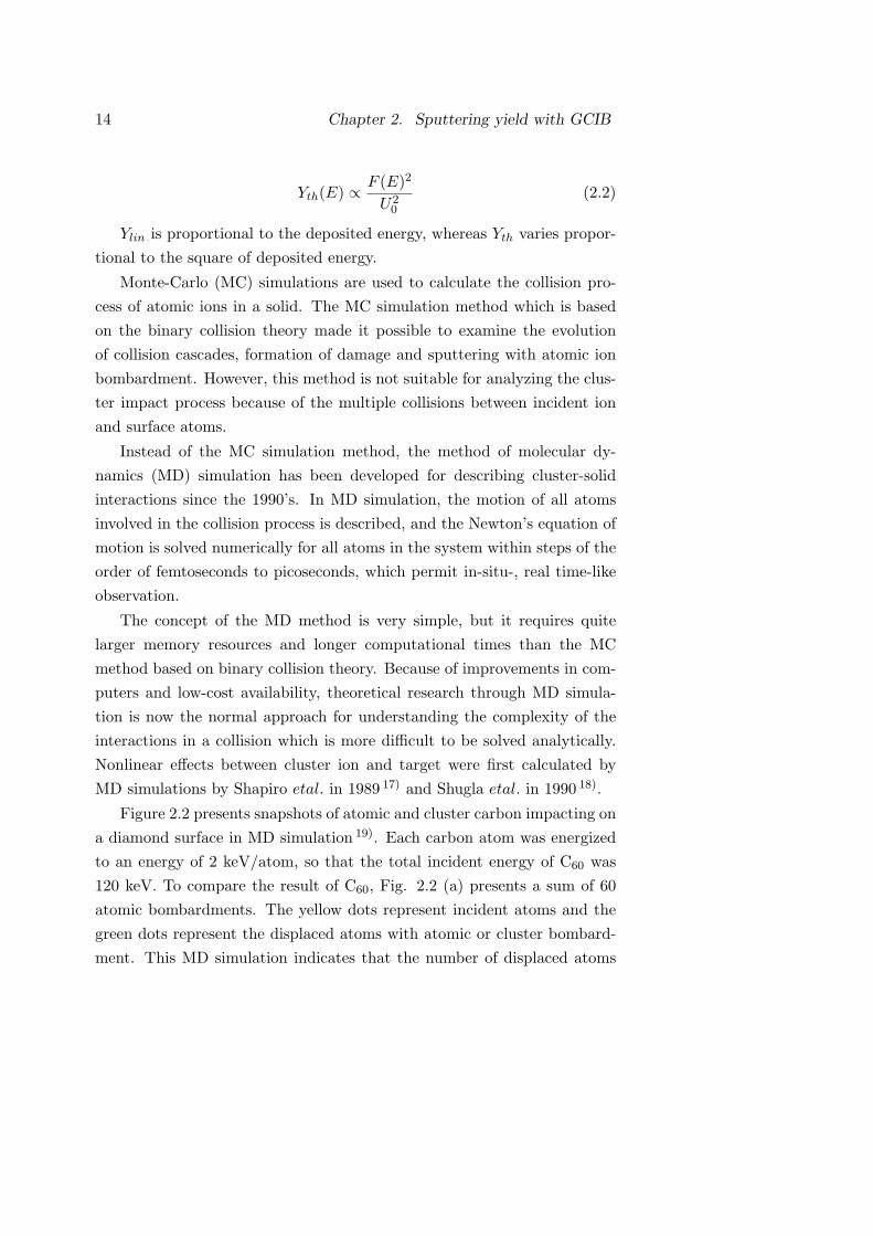
Figure 2.2 presents snapshots of atomic and cluster carbon impacting on
a diamond surface in MD simulation 19). Each carbon atom was energized
to an energy of 2 keV/atom, so that the total incident energy of C60 was
120 keV. To compare the result of C60, Fig. 2.2 (a) presents a sum of 60
atomic bombardments. The yellow dots represent incident atoms and the
green dots represent the displaced atoms with atomic or cluster bombard-
ment. This MD simulation indicates that the number of displaced atoms

2.1. Sputtering effects of ion beam bombardment 15
Figure 2.2: MD simulation of atomic bombardment and cluster bom-bardment into diamond with 2 keV/atom incident energy 19)
was much higher with cluster than the sum of individual atomic impacts,
and the penetration depth of C60 was as deep as C at the same velocity,
indicating that the number of displaced atoms would increase non-linearly
with increasing incident cluster size and it agrees with the experimental
results.
Understanding the physics of energetic cluster bombardment near the
surface is very important, and the sputtering phenomenon is strongly re-
lated to the energy deposition process. Under small (≤ 10 atoms/ion)
cluster ion bombardment, these nonlinear effects were reported to be exper-
imentally a function of cluster size 15, 20, 21). In contrast, there were only a
few reports investigating the nonlinear effects under large (≫ 100atoms/cluster)
cluster ion bombardment.
In this chapter, we investigate the sputtering yield and cluster effects
for sputtering under bombardment with large gas cluster ions.
16 Chapter 2. Sputtering yield with GCIB
2.2 Size select GCIB irradiation
As mentioned in section 2-1, it was believed that large clusters would be
more efficient in inducing the nonlinear effect. Gas clusters consist of more
than several hundreds of atoms and are much larger than typical metal or
carbon clusters. However, the nonlinear effects of the large gas clusters
could not be measured precisely because of a number of reasons.
1. A typical gas cluster ion is too slow to be compared with atomic ions.
Each constituent atom of typical gas cluster has energy of a few 10eV,
which is below the threshold energy for sputtering with atomic ion
bombardment, but nonetheless high sputtering yields are obtained
with GCIB. To compare the irradiation effect of GCIB with that of
an atomic ion at the same energy-per-atom, high energy and small
gas cluster ions are required.
2. GCIB has a very broad size distribution and therefore it is very dif-
ficult to investigate the irradiation effects of a cluster of specific size.
The mean gas cluster size can be roughly controlled by inlet gas pres-
sure and ionization condition However, without size selection, the
GCIB size distribution can extend from about a few to several thou-
sand atoms.
It was reported that the sputtering yields with GCIB strongly depends
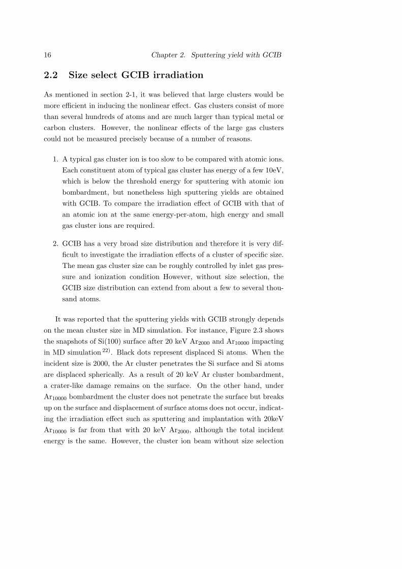
on the mean cluster size in MD simulation. For instance, Figure 2.3 shows
the snapshots of Si(100) surface after 20 keV Ar2000 and Ar10000 impacting
in MD simulation 22). Black dots represent displaced Si atoms. When the
incident size is 2000, the Ar cluster penetrates the Si surface and Si atoms
are displaced spherically. As a result of 20 keV Ar cluster bombardment,
a crater-like damage remains on the surface. On the other hand, under
Ar10000 bombardment the cluster does not penetrate the surface but breaks
up on the surface and displacement of surface atoms does not occur, indicat-
ing the irradiation effect such as sputtering and implantation with 20keV
Ar10000 is far from that with 20 keV Ar2000, although the total incident
energy is the same. However, the cluster ion beam without size selection

2.2. Size select GCIB irradiation 17
20keV Ar2000 → Si(100) 20keV Ar10000 → Si(100)
Figure 2.3: MD simulation of Si sputtering with 20 keV Ar2000 and Ar1000022)
contains clusters of various sizes, and therefore the irradiation effects of the
unselected cluster would be a mixture of effects of various sizes.
To investigate the irradiation effects of a cluster of specific size, the
incident cluster has to be selected in some way. There are various methods
for cluster size separation, but it has been difficult to obtain both high ion
current and high size resolution after size selection. The application of a
E×B filter for size separation has been reported 23), but the size resolution
by this technique was not satisfactory.
The irradiation effect with size-selected gas cluster beams by using a
strong magnet has been also studied. However, the magnetic field intensity
needed to bend same-energy ions is proportional to the square root of the
incident ion size, and therefore it is difficult to select the large ions by using
magnetic fields.
Toyoda etal. reported that both strong magnetic field (1.2 T) and long
effective field length (450 mm) are necessary to realize separation of the
large gas cluster ion beam in high size resolution 24, 25). The cluster size
was selected in this study with the time-of-flight (TOF) method, because
it can accurately select the wished incident cluster size irrespective of its
number of constituents.

18 Chapter 2. Sputtering yield with GCIB
Figure 2.4: Photograph of GCIB irradiation equipment
A photograph of the GCIB irradiation apparatus is shown in Fig. 2.4
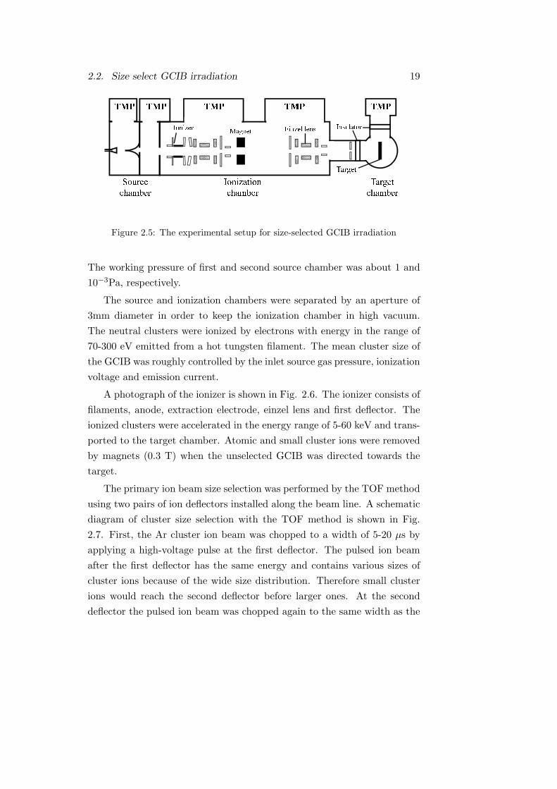
and a schematic view of this equipment is shown in Fig. 2.5. The apparatus
consists of source, ionization and target chambers. Each chamber was put
under vacuum by a turbo molecular pump and the base pressure was about
1 × 10⁻⁵ Pa. Adiabatic expansion of a high pressure gas through a nozzle
is used to form Ar gas clusters, whicn are introduced into the second source
camber via the skimmer.
The throat of the nozzle and the orifice of the skimmers in this equip-
ment were of 0.1 and 1 mm in diameter respectively. The inlet pressure
of Ar gas was 0.4-1.0 MPa and gas flow rate was about 400-700 sccm.
2.2. Size select GCIB irradiation 19
Ionizer Magnet Einzel lens InsulatorMagnetTarget
TMP TMPTMP TMP TMPSourcechamber TargetchamberIonizationchamber
Figure 2.5: The experimental setup for size-selected GCIB irradiation
The working pressure of first and second source chamber was about 1 and
10−3Pa, respectively.
The source and ionization chambers were separated by an aperture of
3mm diameter in order to keep the ionization chamber in high vacuum.
The neutral clusters were ionized by electrons with energy in the range of
70-300 eV emitted from a hot tungsten filament. The mean cluster size of
the GCIB was roughly controlled by the inlet source gas pressure, ionization
voltage and emission current.
A photograph of the ionizer is shown in Fig. 2.6. The ionizer consists of
filaments, anode, extraction electrode, einzel lens and first deflector. The
ionized clusters were accelerated in the energy range of 5-60 keV and trans-
ported to the target chamber. Atomic and small cluster ions were removed
by magnets (0.3 T) when the unselected GCIB was directed towards the
target.
The primary ion beam size selection was performed by the TOF method
using two pairs of ion deflectors installed along the beam line. A schematic
diagram of cluster size selection with the TOF method is shown in Fig.
2.7. First, the Ar cluster ion beam was chopped to a width of 5-20 µs by
applying a high-voltage pulse at the first deflector. The pulsed ion beam
after the first deflector has the same energy and contains various sizes of
cluster ions because of the wide size distribution. Therefore small cluster
ions would reach the second deflector before larger ones. At the second
deflector the pulsed ion beam was chopped again to the same width as the

20 Chapter 2. Sputtering yield with GCIB
Figure 2.6: Photograph of the ionizer
Pulsingvoltage
1st deflector 2nd deflectorPulsingvoltage
Small and SwiftLarge and Slow Specific size
Figure 2.7: Schematic diagram of cluster size selection with the TOF method
first pulse after an appropriate time delay from the first pulse. The pulsed
ion beam at the second deflector contained a specific size of cluster ions
depending on the delay time (tD) between the two pulses. The flight length
between the first and second deflectors was of 1000 mm.
The selected Ar cluster size N is proportional to Va and t2D, where Va
is the acceleration voltage. For instance, the flight time of 20 keV Ar1000
from first to second deflector is of 102 µs, and that of 20 keV Ar4000 is of
204 µs.
Figure 2.7 shows the cluster size distributions of the unselected and size-
selected Ar cluster ion beam. The full width at half maximum (FWHM) of

2.2. Size select GCIB irradiation 21
0 2000 4000 6000 8000 100000.0
0.1
0.2
0.3
0.4
Inte
nsity
(a.u
.)
Cluster size (atoms)
Non-selected
Size selected cluster Mean size 1000 Mean size 2000 Mean size 4000
Figure 2.8: Cluster size distributions of the unselected and size-selected Ar cluster ions
the size distribution of the cluster ion beam without size selection was about
2000 atoms, and that of the size-selected cluster ion beams was about a few
hundred atoms, about 10% of the original distribution. The size resolution
(M/∆M) of the size-selected cluster ion beam can be controlled by tD and
the pulse width of first and second deflectors. The electrostatic einzel lens
installed in front of the second deflector was used for focusing the ion beam
to a 1 mm spot on the target.
The primary ion beam was incident on the target at an angle of 0 degree
with respect to the surface normal. The ion beam current was measured
in the target chamber. The target chamber was separated from ionization
chamber by an insulator and served as a Faraday cup during irradiation.
The working pressure in the ionization and target chamber was 1 × 10⁻⁴Pa.
The repetition frequency was 5000 Hz and the current intensity was from
0.5 to 5 nA after size selection. The current density of the unselected
cluster ion beam was higher than 100 µA/cm2. The maximum current
density of the size-selected cluster ion beam was about 500 nA/cm2 for

22 Chapter 2. Sputtering yield with GCIB
Ar1000 irradiation, and the current density was maintained at about 50
nA/cm2 for Ar16000 irradiation. The sputtering yields of Si as the inorganic
target and polymethylmethacrylate (PMMA) as the organic target were
investigated under impact of the Argon GCIB at various conditions.
2.3. Results-Si target 23
2.3 Results-Si target
The cluster ion beam was not scanned during irradiation of the Si sample,
in order to save irradiation time.
The crystal orientation of the Si substrate was (100). The etched vol-
ume was measured ex situ by an interferometric surface profiler (Maxim-
NT, Zygo, USA) and a contact surface profiler (Dektak3, Veeco, New York,
USA). The observation area was 2.6 mm × 2.4 mm and the spatial resolu-
tion was 10 µm (x, y axes) and 0.1 nm (z axis) respectively.
Figure 2.9 shows a typical example of a surface profile image for the Si
surface irradiated with 20 keV unselected Ar cluster ions with a mean size
of 2000 atoms/cluster at an irradiation dose of 3 × 10¹³ ions. The sputtered
volume was calculated directly from the surface profile because of the high
depth resolution. The sputtered depth of the Si sample irradiated with un-
selected GCIB with scanning was measured with an interferometric surface
profiler and with contact surface profiler measurement and the results of
the two measurements were in good agreement.
Figure 2.10 shows the variation in sputtered volume of Si with an irra-
diation dose of a 20 keV Ar GCIB. The sputtered volume was proportional
to the irradiation dose, indicating that the sputtering yield can be evalu-
ated by the surface profiles and Ar cluster ion dose, even if the irradiation
dose was as small as 1 × 10¹³ ions. From this proportionality constant,
the Si sputtering yield with 20 keV Ar cluster was estimated to be about
35atoms/ion.
In irradiation experiments for size-selected Ar cluster ions, the dose used
was higher than 5 × 10¹³ ions. The effects of incident cluster size on Si
sputtering yield for 20, 40 and 60 keV Ar cluster ions are shown in Fig.
2.11.
Under bombardment with 40 keV Ar1000, more than 200 Si atoms were
sputtered, and this sputtering yield was more than 100 times higher than
that with 40 keV Ar atomic ions. The sputtering yields decreased with in-
creasing cluster size because of the lower incident energy of each constituent
atom. The sputtering yield of 40 keV Ar4000 was still higher than about
70 atoms/ion, and 40 keV Ar16000 was about 40 atoms/ion, i.e. 20 times

24 Chapter 2. Sputtering yield with GCIB
Figure 2.9: The surface profile of Si measured with an interferometricsurface profiler after irradiation with 20 keV unselected Ar GCIB withmean size of 2000 atoms/cluster at the fluence of 3 × 10¹³ ions
0 2 4 6 8 100
1
2
3
4
irradiation ion dose (x 1013 ions)
Sput
tere
d vo
lum
e (x
1013
nm
3 ) 20 keV Ar cluster ion beam => Si
Figure 2.10: Variation of sputtered volume of Si with irradiation dosefor 20 keV Ar cluster ions

2.3. Results-Si target 25
100 1000 100000
100
200
300
400
500
600
Total energy 60 keV 40 keV 20 keV
Sput
terin
g yi
eld
(ato
ms/
ion)
Cluster size (atoms)
Figure 2.11: Si sputtering yield with varying incident cluster size for20, 40 and 60 keV Ar cluster ions
higher than with 40 keV Ar atomic ions. The energy of each constituent
atom for 40 keV Ar16000 was about 2.5 eV, which is lower than the sur-
face binding energy of Si (about 4.6 eV 26)), and this is assumed to result
from the multiple collisions between the cluster ion constituents and surface
atoms.
Figure 2.12 shows the sputtering yields of Si with Ar cluster ions. The
solid squares present the sputtering yields for 20-60 keV unselected Ar clus-
ter ions and the mean size of incident cluster ions was 2000 atoms/cluster.
The sputtering yields of Si with Ar clusters increased non-linearly with
acceleration voltage. These sputtering yields (Y ) for cluster ion beams
containing various sizes of clusters can be represented as:
Y =
∫Y (n)I(n)dn∫
I(n)dn(2.3)
where n is the number of constituent atoms, I(n) is the beam intensity of
the n-size cluster ions and Y (n) is the sputtering yield for the n-size cluster

26 Chapter 2. Sputtering yield with GCIB
0 20 40 60 800
100
200
300
400
500
600 nonselect ion estimated sputtering yield
Sput
terin
g Y
ield
(ato
ms/
ion)
Acceleration Energy (keV)
Figure 2.12: The sputtering yields of Si with 20-60 keV Ar cluster ion
ion. Open circles in the figure present the calculated sputtering yields from
this equation. As clearly shown in Fig. 2.12, the calculated yields agreed
well with the yields for unselected Ar cluster ions, and this indicates that
the irradiation effects under the incidence of clusters of varying size can be
reproduced by the sputtering yield integral for each size of cluster ions. It
also shows that the cluster size selection with the TOF method is useful for
investigating irradiation effects with large cluster ions.
Figure 2.13 shows the variation in sputtering yield for various sizes of
Ar cluster ion and energy per atom. The dotted and solid lines represent
the experimental data and the approximated curve. There was a threshold
incident energy-per-atom to cause sputtering of the target, and the thresh-
old energy depends precisely on the incident cluster size. For example, the
threshold energy for sputtering was about 5 eV/atom under Ar1000 bom-
bardment, and 1 eV/atom under Ar16000 bombardment. It would be natural
that the threshold energy is dependent on incident cluster size, because the
threshold energy for sputtering with Ar atomic ion is about 25eV.
The effect of incident cluster size on Si sputtering and displacing thresh-
old energy shows in Figure 2.14. The solid circles represent experimental
results and open triangles represent the threshold energy for Si displace-
ment energy in MD simulation 27). Each of the threshold energies decreased

2.3. Results-Si target 27
0 5 10 15 20 250
20
40
60
80
Sput
terin
g yi
eld
(ato
ms/
ion)
Incident energy per atom (eV/atom)
cluster size 1000 2000 4000 8000 16000
Figure 2.13: Si sputtering yield with cluster ion bombardment at lowenergy per atom
with increasing incident cluster size in a similar way. The dotted line rep-
resents the simple power law equations where power index was 1/3, and
they are in good agreement with experimental and simulation results. This
power index can be quantified as the volume of damage region. If the aspect
ratio of the damage region does not change as a function of cluster size,
it can concluded that the deposited energy density is proportional to the
cube root of the incident cluster size.
Figure 2.15 shows the sputtering yield of various sizes of Ar cluster as
a function of the incident energy. The sputtering yield and incident enregy
was normarized to the dimension of damage region (N2/3) and the energy
density (N−1/3), respectively. The red-dotted line represents the incident
energy dependence of F 2 where F is the deposited energy. As can be seen
in the figure, the incident energy-per-atom effect on Si sputtering yield is
in good agreement with the square of the deposited energy.
As will be mentioned in the following section, the sputtering yield by
linear collision cascade model is proportional to the deposition energy, and
that by thermal spike model is proportional to the square of the deposition
energy. This result indicates that GCIB irradiation induces thermal spike

28 Chapter 2. Sputtering yield with GCIB
1 10 100 1000 100001
10
Experimental results MD simulation (displacement)
Thre
sold
ene
rgy
(eV
/ato
m)
Cluster size (atom)
Ar cluster => Si
N1/3
Figure 2.14: Si sputtering threshold energy with varying cluster size
100 100010-2
10-1
100
101
F(E)2
Si sp
utte
ring
yiel
d / N
2/3 (a
.u.)
Incident energy per atom x N1/3 -Eth(a.u.)
cluster size 1000 2000 4000
Figure 2.15: Si sputtering yield with varying incident energy cluster ions

2.3. Results-Si target 29
0 50 100 150 200 25010-3
10-2
10-1
100
101
Ar atomic ion Oostra Zalm Balooch TRIM
60 keV 40 keV 20 keV
Sput
terin
g yi
eld
(ato
ms/
atom
)
Incident enregy per atom (eV/atom)
Figure 2.16: The nonlinear effects of Si sputtering with Ar GCIB irradiation
on the surface.
Figure 2.16 shows the sputtering yields of Si per incident atom with
Ar cluster and atomic ions as a function of incident energy per atom. The
yields per atom with Ar cluster ion beams were calculated by the total
yield divided by cluster size. Blue dots represent the experimental results
of Ar atomic ion reported by Oostra etal. in 1987 28), Zalm in 1983 29) and
Balooch etal. in 1996 30), and the blue-dotted line represents the sputtering
yield calculated in this work with TRIM. In both cluster ion and atomic ion
bombardment, the sputtering yield increased rapidly with increasing inci-
dent energy per atom near the sputtering threshold energy, and saturated
under a few hundreds eV/atom. The Si sputtering yield is about 0.2 atoms
with 200 eV Ar atomic ion bombardment and about 1.8 atoms with 200
eV/atom Ar cluster ion bombardment (60 keV Ar300). This result suggests
that the sputtering enhancement with Ar300 would be 9.
Figure 2.17 shows the Si sputtering enhancement factor with B18 and
C60 as reported by Tanjo and Hill etal. 31),respectively. As shown, the
enhancement factor with B18 was 11 and with C60 was 10. This result sug-

30 Chapter 2. Sputtering yield with GCIB
1 10 100 1000 100001
10
100
Ar cluster 200 eV/atom 166 eV/atom 120 eV/atom
250 eV/atomC
60 => Si
Sput
terin
g en
hanc
emen
t fac
tor
Cluster size (atoms)
2 keV/atomB
18 => Si
Figure 2.17: The nonlinear effects of sputtering with varying clusterion bombardment
gests that the enhancement factor with cluster ion would increase rapidly
with increasing cluster size under small cluster (N≤ 20) bombardment, and
saturate at around 10.
In MD simulation, the correlation between the number of displaced
atoms and size has also been reported for carbon cluster bombardment 32).
The number of displacements caused by atomic impact shows first an in-
crease and then a decrease towards the end because some of the displaced
atoms are recovered into the lattice. On the other hand, the number of
displacements caused by cluster impact only increases because of the high-
density energy deposition. When an energetic ion bombards to the surface,
the incident atom energizes to the surface atoms. Under atomic ion bom-
bardment, some of atoms are displaced permanently and trigger damage,
but most of them are only excited. Under small cluster ion bombardment,
the cluster is broken and the constituents are scattered on the local area.
Then, excited areas start to overlap and some of the excited atoms are
finally displaced and trigger damage. Therefore, the number of displaced
atoms increases nonlinearly under cluster ion bombardment. These nonlin-
ear effects increase with increasing incident cluster size because all of the
excited areas becomes damaged areas.
2.3. Results-Si target 31
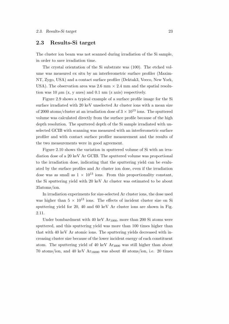
The nonlinear effects with large cluster are saturated because the entire
irradiated area would be no longer excited, and the number of displaced
atoms is proportional only to the incident energy. For Si, the ratio between
damaged and excited atoms with atomic ion bombardment is 9:1.
Figure 2.18 represents the experimental results and calculation curve of
Si sputtering yield with Ar cluster ion bombardment. The sputtering yield
can be expressed as the product of the sputtering yield with atomic ion and
enhancement factor(E/N ≥ 25eV) or the square of the depositted energy
(E/N ≤ 25eV). Therefore, the calculated sputtering yield can represented
as follows.
Yc(E,N) = k(N)×Y (E/N+Eth.a−Eth.c) = 9×N×Y (E/N+Eth.a−Eth.c),
(2.4)
for the high energy cluster ions (E/N ≥ 25eV), and
Yc(E,N) = α×N2/3 × (E/N ×N1/3 − Eth.a)2, (2.5)
for the low energy cluster ions (E/N ≤ 25eV). E, N , k and Eth rep-
resents the total energy, the cluster size, the enhancement factor and the
sputtering threshold energy, respectively.
The enhancement factor of gas cluster ion would be of a constant value,
9. The dotted lines describe this calculation results, and these curves are
in good agreement with the experimental results.
32 Chapter 2. Sputtering yield with GCIB
100 1000 100000
100
200
300
400
500
600
Cluster size (atoms)
10kV 20kV 30kV 40kV 50kV 60kV
Sput
terin
g yi
eld
(ato
ms/
ion)
Figure 2.18: Model of Si sputtering yield with Ar cluster ion
2.4 Results-PMMA target
For organic materials, it has also been reported that the sputtering yields
are enhanced by one order of magnitude by using GCIB. Moreover, gas
cluster ion bombardment onto organic materials has attracted interest not
only because of the high sputtering yield, but also because of the constant
sputtering rate.
Atomic ion bombardment causes chain scission, cross-linking and car-
bonization of polymeric surfaces because of the large energy transfer for
organic materials 33, 34, 35). In other words, under atomic ion bombardment
irradiation damage accumulates on the underlying surface. Small cluster
ion beams, such as SF5+ and C60
+ can reduce the surface damage and the
sputtering rates with small cluster ions are sufficiently high 36, 37). How-
ever,these small cluster ions do not work well for constant etching on some
polymeric materials, such as polycarbonate (PC) and polystyrene (PS) be-
cause of carbon deposition and damage accumulation 38, 39). In contrast,
with GCIB, constant etching rates with little or no damage to the un-
2.4. Results-PMMA target 33
0 1 2 3 4 50
20
40
60
80
100
120
Ar cluster ion
Ar atomic ion
Sput
terin
g de
pth
(nm
)
Irradiation ion fluence (x1015 ions/cm2)
5.5 keV PMMA
Figure 2.19: Variation in sputtered depth of PMMA with irradiationdose for 5.5 keV Ar cluster and atomic ions
derlying structure have been reported for various organic and polymeric
materials such as leucine, arginine, PC, PS and PMMA 40, 41, 42).
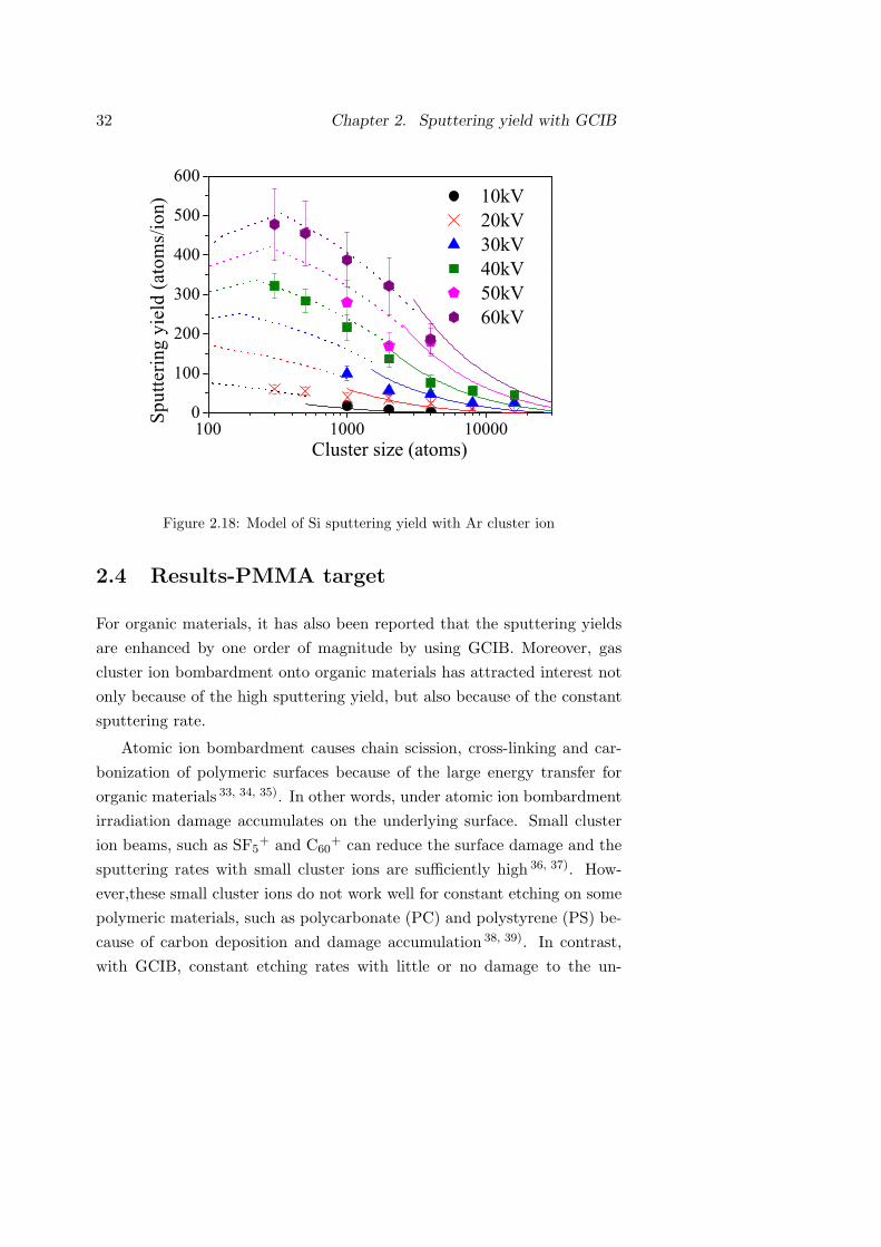
Figure 2.19 shows the etching depth of PMMA with 5.5 keV Ar atomic
ion and cluster ion beam 41). The sputtering rate of PMMA with atomic
Ar+ incidence decreased with increasing fluence. It could be considered that
the chemical transformation of PMMA to a carbon-rich material causes the
decrease in sputtering rate with fluence. In contrast, the sputtering depth
of PMMA with Ar cluster ion shows linear dependence on fluence and more
than 10 times that with Ar atomic ion at low fluence. In view of this, GCIB
is proposed as one of the solutions to the problem of sputtering of organic
and polymeric materials at high speed without damage.
For irradiation of organic materials, the sample was mounted on a scan-
ning stage and rastered for uniform etching. PMMA (repeat unit mass of
100 u, molecular weight (Mw) 700,000-750,000 u; Nacalai Tesque Inc. (Ky-
oto, Japan)) was dissolved in toluene as a 2-5 wt% solution. PMMA thin
films were prepared by spin coating on a Si substrate (10 mm × 10 mm)
with a thickness of about 100-300 nm. The irradiation ion fluence was 2
× 1013-1 × 10¹⁴ ions/cm2 and the etching area was 4 mm × 5 mm. The
etching depth was measured ex situ with a contact surface profiler.

34 Chapter 2. Sputtering yield with GCIB
0.0 0.5 1.0 1.5 2.0-50
-40
-30
-20
-10
0
10
20
Dep
th [
nm ]
Distance [mm ]
10 keV Ar cluster -> PMMA1 x 1014ions/cm2
Figure 2.20: Surface profile image of PMMA irradiated with 10 keVAr cluster ion
Figure 2.20 shows the surface profile image of the PMMA surface irradi-
ated by 10 keV Ar cluster ion. The irradiation dose was 1 × 10¹⁴ ions/cm2
and the estimated etching depth was about 40 nm. The sputtering yield of
PMMA was calculated from the etched depth and ion fluence assuming a
PMMA density of 1.2 g/cm3, and was about 400 units/ion.
Figure 2.21 shows the effects of incident Ar cluster size on PMMA sput-
tering yield for 20 keV Ar (black dots) and C cluster ions (red square) 37).
The PMMA sputtering yield with Ar cluster was higher than with C clus-
ter. The sputtering yields with size-selected Ar cluster ion beam decreased
with increasing cluster size, and this decrease is attributed to the lower
energy of each constituent atom. The sputtering yield with 20 keV Ar16000
was maintained relatively high, but the energy of each constituent atom for
20 keV Ar16000 was only 1.25 eV, which is lower than the value of the bond
energy, for example C-C bonding (about 3.5 eV) in PMMA.
The threshold energy per atom for PMMA sputtering was estimated
to be less than 1 eV/atom with 20 keV Ar cluster ion bombardment, and
this could be attributed to the effect of multiple collisions between the
cluster ion and surface atoms. The Si sputtering yield with Ar cluster
increased monotonously with increasing incident energy-per-atom, but in

2.4. Results-PMMA target 35
100 1000 100000
200
400
600
800
1000
1200
1400Sp
utte
ring
yiel
d (u
nits
/ion)
Cluster size (atoms)
20 keV Ar cluster -> PMMA
100 10 1
Incident enegy per atom (eV/atom)
20 keV C60
Figure 2.21: Variation in PMMA sputtering yield with incident Arcluster size for 20 keV Ar cluster ions
contrast PMMA sputtering yield remained about the same under cluster
ion bombardment in the range of Ar1000 to Ar4000.
Figure 2.22 shows the effects of incident Ar cluster size on PMMA sput-
tering yield for 5-30 keV Ar cluster ions. As shown, PMMA sputtering
yields increased with increasing incident energy per atom up to 10 eV/atom
and saturated independent of the total energy. The saturated value with
20 keV Ar cluster was about 1000 units/ion, and the energy efficiency for
sputtering with this condition was only 20 eV/unit, suggesting that more
than 20 % of displaced PMMA units were ejected from the surface. This
value is much higher than the sputtering probability of an inorganic target
such as Si, which was less than 1 %, and therefore the sputtering yield
with small cluster ion would be saturated in PMMA. This effect of incident
energy on the sputtering yields of organic targets has been observed earlier
in MD simulations 43, 44), and is in good agreement with this experimental
result.
Figure 2.23 shows PMMA sputtering yield with Ar1000 and Ar4000 as a

36 Chapter 2. Sputtering yield with GCIB
1 10 1000
500
1000
1500
30keV 20keV 10keV 5 keV
Sput
terin
g yi
led
(uni
ts/io
n)
Incident energy per atom (eV/atom)
Figure 2.22: Variation in PMMA sputtering yield with varying inci-dent Ar cluster energy-per-atom for 5-30 keV Ar cluster ions.
function of incident energy per atom. The threshold energy for sputtering
with Ar1000 and Ar4000 was estimated from approximated curves to be
about 2.5 and 1.5 eV, respectively, indicating that the threshold energy
decreased with increasing incident cluster size, and this is similar to the
results of Si sputtering. As shown, the sputtering yield increased linearly
with the incident energy per atom, indicating that the incident energy was
mostly used for sputtering PMMA, and the efficiency of sputtering was
independent of the incident energy per atom.
It would be easy to control the etching rate by controlling the incident
cluster size and energy per atom. In terms of fast etching with GCIB, fast
and large clusters would be the optimum cluster condition.

2.4. Results-PMMA target 37
0 5 10 15 20 25 30 350
1000
2000
3000
4000
5000
Ar1000
Sput
terin
g yi
eld
(uni
ts/a
tom
)
Incident energy per atom (eV/atom)
Ar4000
Figure 2.23: Variation in PMMA sputtering yield with varying energyper atom for Ar1000 and Ar4000 clusters.


Chapter 3
Secondary ion emission with GCIB
3.1 Secondary ion mass spectrometry
When energetic ions bombard a solid surface, some particles are emitted
from the surface, as mentioned in chapter 2. The sputtered particles emitted
from the surface are mostly neutral, with less than one percent being in a
charge state called “secondary ions”.
The existence of ionized particles when sputtering various surfaces was
first documented by J.J. Thomson in 1910, but it took about 30 years to
build an instrument capable of measuring the emitted ions. These emitted
ions, called “secondary ions” are easy to detect using various means and can
help understanding the surface structure. For this reason, the Secondary
Ion Mass Spectrometry (SIMS) technique has been one of the most popular
and useful surface analysis methods. SIMS has been also applied in the
investigation of irradiation effects of GCIB because detected secondary ions
reflect both the surface structure of the target and the irradiation effects of
the incident cluster.
Under cluster ion bombardment, the “nonlinear effects” have been only
observed not only for sputtering yield, but also for secondary ion yield.
For instance, SIMS with cluster ions such as Au+3 , C+60 has been frequently
studied, and numerous experimental results have shown that secondary ion
yields are significantly enhanced by cluster ion impact.
Thomas etal. reported in 1985 on the secondary ion yield of CsI with
H cluster 45); they found that the enhancement effect of cluster ion for
secondary ion emission was similar or higher than that for sputtering.
39

40 Chapter 3. Secondary ion emission with GCIB
Benguerba etal. reported on the secondary ion yield of gold and some other
molecules with Au and CsI clusters in 1991 46); they found that the en-
hancement factor depends not only on cluster size but also on the target
material. In their work, the enhancement of the secondary molecular ions
yield was higher than that of the secondary atomic ions yield, suggesting
that large secondary ions are more efficiently detected when using large
cluster ions.
Unique irradiation effects have also been reported for secondary ion
emission under large gas cluster ion bombardment. Figure 3.1 represents
the secondary ion spectra of Si with obtained with Ar atomic ion and Ar
cluster ion at an energy of 20 keV 47). Under bombardment with Ar cluster
ions, Si cluster ions such as Si2+ and Si3
+ appeared with high intensity.
On the other hand, their intensity is very low when using atomic Ar ions.
Meanwhile, that triggers the emission of multiply charged ions such as
Si2+ and Si3+. There were however never observed using Ar cluster ion
bombardment. This indicates that the secondary ion was ejected more
softly by GCIB bombardment, the amount of energy transferred to the
ejected particles being too low to allow for multiple charging. In this chapter
we investigates the effect of the primary Ar cluster size and energy-per-atom
on secondary ion emission, and discuss the energy deposition and emission
processes of secondary ions under large cluster ion bombardment.
3.2 Size-selected cluster SIMS
3.2.1 Time-of-flight mass spectrometry
Mass spectrometric techniques provide information about the mass-to-charge
ratio (m/z) of charged particles generated from a target sample. The mass-
to-charge ratio can be measured with various methods, namely time-of-
flight (TOF), magnetic sector, quadrupole mass spectrometer, and Fourier
transform ion cyclotron resonance.
In this SIMS analysis, secondary ions were measured using a TOF mass
spectrometer (MS) because of its simple instrumentation and ability to
detect all ions at one time, even in the high-mass range (in principle, up to
infinity). The principle of a TOF instrument is described below.

3.2. Size-selected cluster SIMS 41
0 40 80 120 160 2000
1
2
3
0 40 80 120 160 2000.0
0.4
0.8
1.2
1.6
(a) 20 keV Ar cluster ion -> Si
Si7
+Si6
+Si5
+Si4
+Si3
+
Si2
+
Si+
Inte
nsity
[ a.
u. ]
(b) 20 keV, Ar atomic ion -> Si
Si2+
m/z
Figure 3.1: Secondary ion spectra of Si obtained with cluster and Aratomic ions at 20 keV 47)
In methods based on TOF-MS, emitted ions are accelerated through an
electric field into a field-free region, and transported to a detector installed
at the end of the field-free region. Light ions fly faster than heavy ions
in the field free region because every ion has same energy, and thus arrive
earlier at the detector. In this experiment, we measured the flight time
only in the field-free region; therefore the calculation of flight time was
very simple. The secondary ion energy E is expressed as
E = zV + E0 (3.1)
where z, V and E0 correspond to the charge of ions, acceleration voltage
and initial energy of the secondary ions, respectively. When energetic ions
fly in the field-free region of length L, the flight time t of the ions is given
by
t = L
√m
2zV + 2E0(3.2)
The mass resolution of the analyzer is defined by the pulse width, ∆tp,

42 Chapter 3. Secondary ion emission with GCIB
the energy distribution leading to a flight time difference ∆tE for different
ions with the same mass, and the precision of the registration system ∆td,
m
∆m=
t
2∆t=
t
2√∆t2p +∆t2E +∆t2d
(3.3)
Because the emitted secondary ion has an energy distribution width of
a few eV, ∆tE is typically the largest of the three, and a reflectron SIMS
system is widely used for reducing ∆tE . However, ∆tp is larger than ∆tE in
gas cluster-SIMS because the GCIB has a wide velocity distribution, and
therefore in this study we measured the time-of-flight by a linear TOF-
SIMS system. In this study, zV was 2 keV and L was 400 mm. For an ion
of m/z 100 the following values were calculated: t = 6.4 µs, ∆tp = 0.1 µs
and ∆tE = 0.02 µs, suggesting that the estimated m/∆m was about 30 in
this SIMS measurement.
3.2.2 Size selected SIMS
Figure 3.2 presents the experimental setup for cluster-SIMS. The basic
setup of the irradiation system was similar to that described in Ch. 2,
but in this system the second primary ion beam deflector was removed.
The target chamber was separated from the ionization chamber with two
apertures for differential evacuation in order to keep target chamber un-
der high vacuum (≤ 10−6 Pa). The secondary ions were measured using a
linear TOF system and detected by a microchannel plate detector(MCP).
Figure 3.3 presents the schematic diagram of the TOF-SIMS technique
for size-selected ions. First, the primary ion beam is chopped to a width of 5
µs by a high-voltage pulse applied between the parallel electrodes installed
along the beam line. Before the pulsed ion beam hits the target, the pulse
widens beyond 100 µs because of the size difference between the incident
cluster ions. The primary cluster ion beam is continuously bombarded onto
the target at an angle of 45 degree with respect to the surface normal, and
secondary ions are emitted. Then, the secondary ions are extracted with
a parallel electrode and reach a secondary ion deflector installed between
the target and the secondary ion detector. This secondary ion deflector is
known as the interleaved comb ion mass deflection gate (Fig. 3.4). The

3.2. Size-selected cluster SIMS 43
TargetTMPTMP TMPTMPTMP
SourcechamberTargetchamber IonizationchamberTMP
Detector
Primary ion deflector
Secondary ion deflector
Figure 3.2: The experimental setup for size-selected SIMS
Figure 3.3: Schematic diagram of the size-selected SIMS
secondary ion deflector consists of two electrically insulated sets of thin
wires mounted parallel to each other and perpendicular to the target surface
normal. The wire diameter is 0.35 mm and the distance between wires is
0.85 mm. Finally, the secondary ion beams are chopped to a width of 200ns
by applying a relatively low voltage pulse between the wires.
We could selectively measure secondary ions produced by different sizes
of cluster ions by changing the time interval (delay time) between the pri-
mary and the secondary ion beam chopping. The pulse repetition rate of
primary ion and secondary ion chopping was 1000-10000 Hz. Secondary ion
were extracted with 2 keV kinetic energy and detected with MCP set on

44 Chapter 3. Secondary ion emission with GCIB
10mmFigure 3.4: The secondary ion deflector
the axis of the surface normal. The incident cluster size resolution of size
selected gas cluster was about the same as that described in Ch. 2.
The cluster size distribution before size-selection is shown in Figure
3.5. In this experiment, the inlet gas pressure was about 0.7 MPa and the
average cluster size was about 1000 atoms. The number of incident cluster
ions was estimated from this size distribution.
Figure 3.6 presents a schematic diagram of the TOF electronics used in
this study. A pulse generator, DG535, generated pulses for both the pri-
mary and secondary ion beam chopping to a high voltage (H.V.) switching
circuit. The pulse to the switching circuit of the secondary ion chopper
was also provided as a start pulse into a fast multi-channel scalar (SRS:
SRS430). The output from the MCP was amplified with an ORTEC 9306
preamplifier and was provided as a stop pulse into MCS.

3.2. Size-selected cluster SIMS 45
0 1000 2000 3000 4000 50000.0
0.2
0.4
0.6
0.8
1.0
1.2
40keV Ar cluster ion
Ion
inte
nsity
[a.u
.]
Cluster size (atoms)
Figure 3.5: Size distribution of Ar cluster ion beam with total energy of 40 keV
Figure 3.6: Schematic diagram of the electronic components used inthis TOF-SIMS

46 Chapter 3. Secondary ion emission with GCIB
3.3 Results-Si target
3.3.1 Secondary cluster ion emission
For irradiation of the Si (100) target, the oxidized surface layer was etched
with Ar GCIB in the high-vacuum (≤ 10−6Pa) target chamber before SIMS
measurements. The incident cluster energy was in the range 10-60 keV and
the cluster size was in the range of 300-2500 atoms/ion.
Figure 3.7 represents the secondary ion spectra obtained under the inci-
dence of 40 keV Ar300(133 eV/atom), Ar600(67 eV/atom) and Ar1100(36eV/atom).
The secondary ion intensity was normalized to the intensity of Si+. Under
40 keV Ar300 bombardment,mainly Si+ ions were detected, and the yields
of Si cluster ions such as Si+3 and Si+4 were extremely low compared to that
of Si+. In contrast, the ratio of Si cluster ion yield was clearly high with 40
keV Ar1100 bombardment, suggesting that the secondary ion species inten-
sities are strongly dependent on the incident cluster condition for the same
total energy.
Figure 3.8 presents the intensity ratio of Si+n /Si+ with 40 keV Ar300,
Ar600 and Ar1100. In this experiment, Si cluster ions were detected with
strong intensities up to Si+11. The cluster ion ratio increased with increasing
impinging cluster size, and this effect was more enhanced for large secondary
ions. For example, the ratios Si+3 /Si+ and Si+9 /Si
+ with Ar1100 bombard-
ment were about 6 and 30 times higher than with Ar300 bombardment,
respectively. One of the possible reasons for the difference is the ioniza-
tion probability of Si atomic and cluster ions. However, the difference in
ionization potential of the Si atom and cluster hardly affects the ratio of
Si cluster ion because the ionization potential of Si atom and clusters were
only in the range of 7.5-8.5 eV.
The probability of cluster particle emission can be calculated by the
ratio of secondary cluster ion and cluster size. The results of this calculation
indicate that about 40 % of Si was emitted as single Si under 40 keV Ar300
bombardment, and only 5 % of Si was emitted as single Si under 40 keV
Ar1100 bombardment. The intensity ratio of the Si cluster decreased with
decreasing secondary cluster size, but that of Si+6 was higher than that of
Si+5 . This experimental result is attributed to the magic number of Si,

3.3. Results-Si target 47
0.20.40.60.81.01.2
0.20.40.60.81.01.2
0 50 100 150 2000.00.20.40.60.81.01.2
Si2
+
133 eV/atom
Si6
+
Si5
+
Seco
ndar
y io
n in
tens
ity [a
.u.]
Si+
36 eV/atom
67 eV/atom
40keV Ar1100
+ Si
40keV Ar600
+ Si
Si4
+Si3
+
m/z
40keV Ar300
+ Si
Figure 3.7: Secondary ion spectra of Si with various sizes of 40 keVAr cluster ions

48 Chapter 3. Secondary ion emission with GCIB
2 4 6 8 10 1210-3
10-2
10-1
100
Si cluster size n [ atoms ]
Ar300
Ar600
Ar1100
Si
n+ /Si+ in
tens
ity ra
tio
40keV Ar cluster Si
Figure 3.8: Secondary Si+n /Si+ intensity ratio with Ar cluster ion
bombardment at 40 keV
and in good agreement with other experimental reports with Au cluster
bombardment and laser ablation 48, 49).
As mentioned in Ch. 2, the irradiation effects were strongly affected by
the incident cluster size and incident energy-per-atom. The incident size
and energy-per-atom effects on secondary cluster ion emission are shown
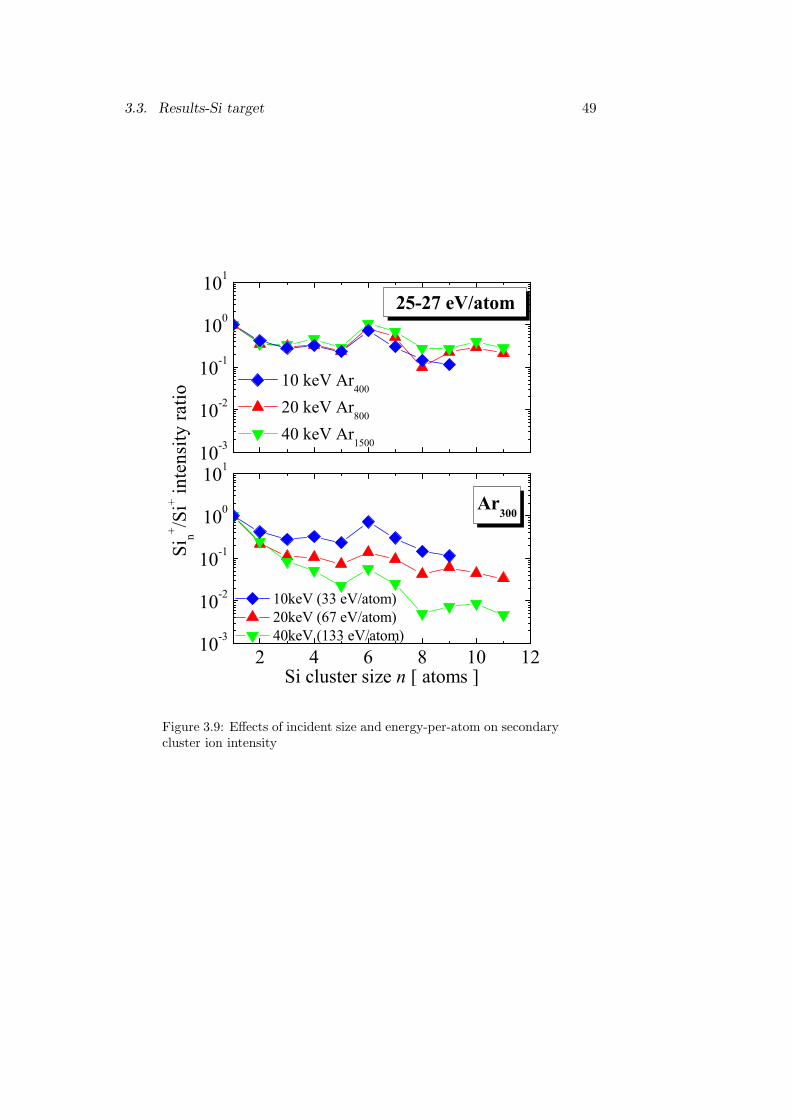
in Figure 3.9. The secondary cluster ion intensity ratio with 10 keV Ar400
and 40 keV Ar1500 bombardment were approximately the same for every
size of Si+n , although the total energy of 40 keV Ar1500 is 4 times higher
than 10keV Ar400. On the other hand, the intensity ratios of the secondary
Ar300 cluster ion with 10 and 40 keV were far from each other. For instance,
the ratio of Si+6 /Si+ with 10 keV Ar300 was 0.72 and this value was more
than one order of magnitude higher than the value of 0.06 obtained with
40keV Ar300. This result indicated that secondary ion emission was strongly
dependent on the energy-per-atom in the incident cluster, and the effect of
the actual incident cluster size would be very small.
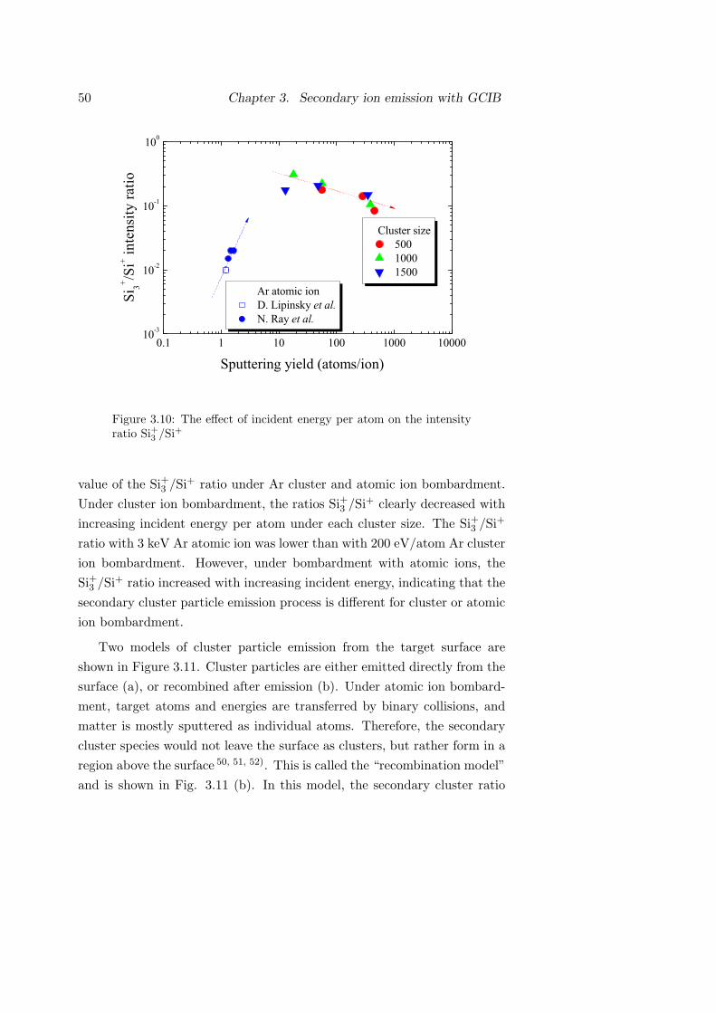
Figure 3.10 presents the effect of the incident energy per atom on the
3.3. Results-Si target 49
10-3
10-2
10-1
100
101
2 4 6 8 10 1210-3
10-2
10-1
100
101
25-27 eV/atom
10 keV Ar400
20 keV Ar800
40 keV Ar1500
Sin+ /S
i+ inte
nsity
ratio
Ar300
10keV (33 eV/atom) 20keV (67 eV/atom) 40keV (133 eV/atom)
Si cluster size n [ atoms ]
Figure 3.9: Effects of incident size and energy-per-atom on secondarycluster ion intensity
50 Chapter 3. Secondary ion emission with GCIB
0.1 1 10 100 1000 1000010-3
10-2
10-1
100
Ar atomic ion D. Lipinsky et al. N. Ray et al.
Cluster size 500 1000 1500
Si3+ /S
i+ inte
nsity
ratio
Sputtering yield (atoms/ion)
Figure 3.10: The effect of incident energy per atom on the intensityratio Si+3 /Si
+
value of the Si+3 /Si+ ratio under Ar cluster and atomic ion bombardment.
Under cluster ion bombardment, the ratios Si+3 /Si+ clearly decreased with
increasing incident energy per atom under each cluster size. The Si+3 /Si+
ratio with 3 keV Ar atomic ion was lower than with 200 eV/atom Ar cluster
ion bombardment. However, under bombardment with atomic ions, the
Si+3 /Si+ ratio increased with increasing incident energy, indicating that the
secondary cluster particle emission process is different for cluster or atomic
ion bombardment.
Two models of cluster particle emission from the target surface are
shown in Figure 3.11. Cluster particles are either emitted directly from the
surface (a), or recombined after emission (b). Under atomic ion bombard-
ment, target atoms and energies are transferred by binary collisions, and
matter is mostly sputtered as individual atoms. Therefore, the secondary
cluster species would not leave the surface as clusters, but rather form in a
region above the surface 50, 51, 52). This is called the “recombination model”
and is shown in Fig. 3.11 (b). In this model, the secondary cluster ratio

3.3. Results-Si target 51
increases with increasing sputtering yield.
Reports of experiments and MD simulations have shown that the cluster
ion ratio increased with increasing sputtering yield under atomic or small
cluster impact 53, 54, 55). On the other hand, in the direct emission model,
cluster particles are emitted from the surface as clusters when many surface
atoms are energized at the same time. In this model, the ratio of cluster
particles decreases with increasing deposition energy because high energy
deposition breaks the secondary clusters. Direct emission of cluster parti-
cles has also been reported in experiments and MD simulations 56, 57, 58).
Experimentally, it has mainly been reported in laser ablation and thermal
evaporation. The deposited energy density with laser ablation is around
100 mJ/cm2, more than one order of magnitude lower than the value for
atomic ion bombardment. Moreover, the sputtering phenomena observed
with energetic atom bombardment result from binary collisions. Therefore,
it would be difficult to obtain direct emission of cluster particles by atomic
ion or small cluster ion bombardment. With large cluster impacts the de-
posited energy density was as large as for laser ablation and the thermal
spike deposits energy to many surface atoms at the same time.
Figure 3.12 represents the value of the Si+3 /Si+ ratio as a function of
deposited energy density by cluster ion bombardment. The incident energy
density was calculated taking into account cluster energy and cluster cross
section. The van der Waals radius of the argon atom was calculated to be
of 0.19 nm. The secondary cluster ion ratio decreased exponentially with
deposited energy density, and this result was in good agreement with reports
on laser ablation. This dependence of secondary cluster intensity ratio on
deposited energy does however not work wwll for high-energy cluster ion
bombardment. Indeed, the sputtering yield with this kind of cluster was
higher than 500 atoms/ion as shown in Ch. 2, therefore recombination
would be as large as direct emission under these conditions.
3.3.2 Enhancement of Si+ emission
Figure 3.13 represents the Si+ yield per incident ion with 40 keV Ar cluster
at various cluster sizes. The Si+ yield was calculated from the secondary
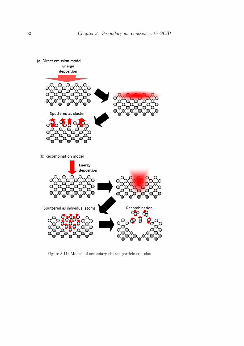
52 Chapter 3. Secondary ion emission with GCIB
Figure 3.11: Models of secondary cluster particle emission

3.3. Results-Si target 53
0 40 80 120 16010-2
10-1
100
Direct emission model
Va(kV) 10 15 20 30 60Si
3+ /Si+ in
tens
ity ra
tio [a
.u.]
Energy density (mJ/cm2)
exp
Figure 3.12: The effect of deposited energy density on the intensityof Si+3 /Si
+ (Va is ‘acceleration energy’)
ion counts and the number of incident cluster ions, as measured from the
cluster size distribution shown in Fig. 3.5. As shown in the Fig. 3.13,
with small clusters the Si+ yield was almost steady and did not vary with
cluster size but was dependent on total energy. Under large cluster ion
bombardment, the secondary ion yield decreased with increasing incident
cluster size and this shows the same tendency as the sputtering yield. Si+
yield with 40 keV Ar cluster was one to two orders of magnitude higher
than that with 40 keV Ar atomic ion bombardment.
The Si sputtering yield with 40 keV Ar cluster was also one to two orders
of magnitude higher than that with 40 keV Ar atomic ion bombardment,
indicating that the ionization probability of sputtered Si with Ar cluster ion
was as large as that with Ar atomic ion, although the incident energy per
atom of Ar cluster ion is much lower than an Ar atomic ion. The ionization
probability is strongly dependent on the incident ion and target species, and
the kinetic energy of the secondary particle. The effect of kinetic energy on
the ionization probability Pi is simply described as follows;

54 Chapter 3. Secondary ion emission with GCIB
1 10000.0
0.2
0.4
0.6
0.8
1.0
1.2
Si+ io
n yi
elds
per
ion
[a.u
.]
Ar cluster size (atoms)
40keV Ar cluster Si 40000 100 10
Incident energy per atom (eV/atom)
Figure 3.13: Si+ intensity with various sizes of 40 keV Ar cluster ion
Pi = exp(−bE−0.5i ), (3.4)
where b is a fitting parameter that depends on the ionization potential
and E is the kinetic energy of the secondary particle 59, 60). The kinetic
energy of the secondary particle would be about the same under Ar atomic
or cluster ion bombardment.
A comparison of the Si sputtering yield and the Si+ yield under 60 and
20 keV Ar cluster ion bombardment is shown in Fig. 3.14. The secondary
ion intensity Yi can be described as
Yi(E) = Pi × Y (E), (3.5)
where Pi is ionization probability and Y is sputtering yield. As shown
in Fig. 3.14(a), the effect of incident energy per atom on secondary ion
and sputtering yield is the same under bombardment at high energy per
atom (≥ 40eV/atom). It indicates that the ionization probability of these

3.3. Results-Si target 55
10 1000.00
0.05
0.10
0.15
0.20
0.0
0.5
1.0
1.5
2.0
Sput
terin
g yi
eld
(ato
ms/
atom
)
Si Sputtering yield
0.0
5.0x10⁻⁶
1.0x10⁻⁵
1.5x10⁻⁵
2.0x10⁻⁵
2.5x10⁻⁵
3.0x10⁻⁵
Incident energy per atom (eV/atom)
Si+ yield
Si+
inte
nsity
(ion
s/at
om)
20 keV Ar cluster => Si
Si Sputtering yield
0.0
5.0x10⁻⁵
1.0x10⁻⁴
1.5x10⁻⁴
2.0x10⁻⁴
2.5x10⁻⁴
3.0x10⁻⁴
(b)
Si+ yield
60 keV Ar cluster => Si
(a)
Figure 3.14: Variation of Si and Si+ yield with incident energy peratom and cluster size for size-selected 20 and 60 keV Ar cluster ionbeams.
clusters is independent on the condition of the incident cluster. As shown
by solid circles in Fig. 3.14 (b), the secondary ion yield decreased with
decreasing incident energy per atom more rapidly than the Si sputtering
yield.
When the energy per atom of the bombarding cluster was higher than
20eV/atom, Si and Si+ were emitted from the Si surface with high intensity.
On the other hand, when energy per atom of the bombarding cluster was
about 10 eV/atom, Si+ ions were rarely emitted, although neutral Si atoms
were still emitted. The threshold energy of incident cluster ion for Si+
emission was estimated to be about 8 eV/atom, which was a few times
higher than the threshold energy for Si sputtering. This difference between
Si and Si+ emissions is attributed to the ionization process of sputtered Si

56 Chapter 3. Secondary ion emission with GCIB
particles.
The ionization energy of Si is 8.16 eV and it is about the same as the
threshold energy per atom of Si+ emission, and much higher than the bind-
ing energy of Si, 3.4 eV. The secondary particle cannot have enough kinetic
energy to ionize under bombardment with cluster ion with low energy per
atom. This result indicates that the surface atoms were easily sputtered
with cluster ion bombardment because of multiple collisions, but the sput-
tered particles couldn’t gain sufficient energy to become ionized when the
energy per bombarding atom was at a value between sputtering and ion-
ization threshold energy and only neutral particles were emitted.

3.4. Results-Organic materials 57
3.4 Results-Organic materials
Atomic ion beams produce weak signals for large organic molecules be-
cause of critical problems, such as low sputtering yield and damage to
biomolecules. Cluster ions such as C+60 and Au+3 have been studied as
primary ions for SIMS 61, 62), because yields of both neutral and ionized
particles increase considerably with cluster size. However, even cluster ions
could not solve the problem of damage to biomolecules caused by incident
ions. GCIB was proposed to be one of the solutions to the problem of
sputtering organic and polymeric materials without damage 63).
Figure 3.15(a, b) presents the mass spectra of positively charged sec-
ondary ions emitted from a leucine (C6H13NO2, 131 u, one of the amino
acids) film with 8 keV Ar cluster and Ar atomic ion, respectively. Pro-
tonated leucine molecular ions (C6H14NO+2 , m/z = 132) and character-
istic fragment ions such as m/z = 44 (CO+2 ) and m/z = 86 (C5H12N
+
or [m-COOH]+) were detected with high intensity. The yields of proto-
nated leucine molecular ions emitted by Ar atomic ions were extremely low
compared to fragment ions. In contrast, the yields of protonated leucine
molecular ions emitted by Ar cluster ions were the same or higher than
those of fragment ions, indicating that large gas cluster ions can sputter
and ionize leucine molecules with little damage. In this section, we inves-
tigate the effect of the bombarding cluster condition on the damage to the
surface and on secondary ion emission in polymethylmetacrylate (PMMA),
tris(8-hydroxyquinoline)aluminum (Alq3), Arginine and Phenylalanine.
Figure 3.16 presents the molecular structure of PMMA, Alq3, arginine
and phenylalanine. PMMA is one of the typical polymeric materials. Its
repeated unit is C5H8O2 (m = 100 u), and its molecular weight (Mw) was
700,000-750,000 in this study. Alq3 is one of the components of organic
light-emitting diodes (OLED). Its composition formula is C27H18AlN3O3
(m = 459.4 u). Arginine and phenylalanine are amino acids, and their
composition formulas are C6H14N4O2 (m = 174 u) and C9H11NO2 (m =
165 u), respectively.
PMMA, arginine and phenylalanine were obtained from Nacalai Tesque
Inc. (Kyoto, Japan). Alq3 was obtained from Chemipro Kasei Kaisha,

58 Chapter 3. Secondary ion emission with GCIB
0
500
1000
1500
0 50 100 150 2000
500
1000
1500(b)
8keV Ar cluster -> leucineIo
n In
tens
ity [a
.u.]
13286(a)
8keV Ar atomic ion -> leucine
m/z
Figure 3.15: Secondary ion spectra of leucine obtained with 8 keV Arcluster and atomic ion bombardment
LTD. (Hyogo, Japan). The PMMA and arginine films were prepared by
spin-casting method, and the Alq3 and phenylalanine films were prepared
by vapor deposition method on clean silicon substrates. The silicon sub-
strate was washed with water, ethanol and acetone in an ultrasonic cleaner.
PMMA was dissolved in toluene as a 2 wt% solution, and arginine was dis-
solved in water as a 15 wt% solution. The thickness of the organic films
was about 100-200 nm.
Figure 3.17 presents the mass spectra of positively charged secondary
ions emitted from the arginine film under bombardment with 11 keV Ar600,
Ar1200 and Ar2500. The secondary ion intensity was normalized to the
intensity of the protonated arginine molecular ion, m/z = 175(C6H15N4O+2
or [m+H]+). Under 11 keV Ar600 bombardment, m/z = 45 and 70 also
had strong intensities, and they were assigned as COOH+ and C4H8N+,
respectively. As shown, the intensity ratio of fragment ions to the arginine
ion decreased with increasing incident cluster size, and the characteristic
fragment ions were hardly detected under 11 keV Ar2500 bombardment,

3.4. Results-Organic materials 59
Figure 3.16: Schematic diagrams of the molecular structures of theorganic targets

60 Chapter 3. Secondary ion emission with GCIB
because the bond association energy of C-O and C-C is stronger than the
van der Waals energy between arginine molecules, and the incident energy
per atom of 11 keV Ar2500 (4.4 eV/atom) was similar to the bond association
energy of C-O and C-C.
Figure 3.18 presents the mass spectra of positively charged secondary
ion emitted from the phenylalanine film with 11 keV Ar600, Ar1200 and
Ar2200. The secondary ion intensity was normalized to the protonated
phenylalanine molecular ion, m/z = 166(C9H12NO+2 or [m+H]+). A char-
acteristic fragment ion was also observed at m/z = 120 (C8H10N+ or
[m+COOH]+). The intensity ratio of fragment ions to the phenylalanine
ion decreased with increasing incident cluster size, like for arginine. In the
case of phenylalanine, protonated phenylalanine dimer (m/z = 331) was de-
tected with Ar cluster ion bombardment. The intensity ratio of the dimer
increased with increasing incident cluster size, and was seen to be as large
as the protonated single phenylalanine under 11 keV Ar2200. The threshold
energy per atom for no-damage processing was the same for phenylalanine
and arginine because these structures are close.
Figure 3.19 presents the intensity ratio between the characteristic frag-
ment ion and the protonated molecular ions of arginine and phenylalanine
targets. The intensity ratio of the fragment ions was about the same under
cluster ion bombardment with high energy per atom (≥20 eV/atom), but
decreased drastically with low energy per atom below 10 eV/atom. Under
cluster ion bombardment with 5 eV/atom, the fragment intensity ratio was
one order of magnitude lower than that of the protonated molecular ion.
Figure 3.20 presents the mass spectra of positively charged secondary
ions emitted from the PMMA film bombarded with 8 keV Ar atomic ions,
Ar500 and Ar2000. The secondary ion intensity was normalized to the inten-
sity of characteristic fragment m/z = 69(C4H5O+ or [m-OCH3]
+). Under
atomic ion bombardment, m/z =55 (C4H+7 ) also had strong intensity, and
the large ion of protonated MMA (m/z=101) was not detected. Under
bombardment with large cluster ions, the protonated MMA ion was clearly
detected. However, the secondary ion spectra with Ar500 and Ar2000 seem
to be similar, and this is different from the results of amino acids. This
could be attributed to the difference in bond energy between PMMA and

3.4. Results-Organic materials 61
0.2
0.4
0.6
0.8
1.0
1.2
0.2
0.4
0.6
0.8
1.0
1.2
0 100 200 300 400 5000.0
0.2
0.4
0.6
0.8
1.0
1.2
Inte
nsity
[a.u
.]
18eV/atom
17570
11 keV Ar600
+ Arginine
11 keV Ar1200
+ Arginine
9eV/atom
11 keV Ar2500
+ Arginine
m/z
4.4eV/atom
Figure 3.17: Secondary ion spectra of arginine with 11 keV Ar clusterion bombardment

62 Chapter 3. Secondary ion emission with GCIB
0.2
0.4
0.6
0.8
1.0
1.2
0.2
0.4
0.6
0.8
1.0
1.2
0 100 200 300 400 5000.0
0.2
0.4
0.6
0.8
1.0
1.2
Inte
nsity
[a.u
.]
166
331
120
m/z
11 keV Ar600+ Phenylalanine
18eV/atom
11 keV Ar1200+ Phenylalanine
9eV/atom
11 keV Ar2200+ Phenylalanine
5eV/atom
Figure 3.18: Secondary ion spectra of phenylalanine with 11 keV Arcluster ion bombardment
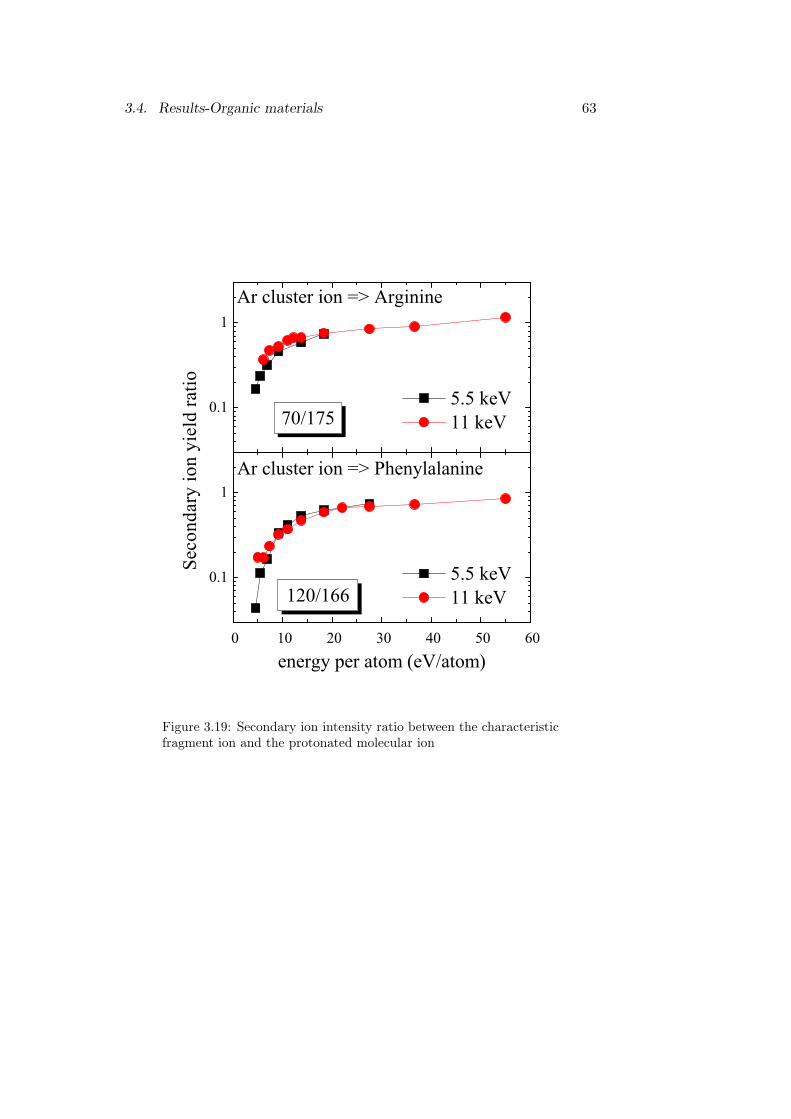
3.4. Results-Organic materials 63
0.1
1
0 10 20 30 40 50 60
0.1
1
120/166
Ar cluster ion => Phenylalanine
Seco
ndar
y io
n yi
eld
ratio
5.5 keV 11 keV
Ar cluster ion => Arginine
70/175
energy per atom (eV/atom)
5.5 keV 11 keV
Figure 3.19: Secondary ion intensity ratio between the characteristicfragment ion and the protonated molecular ion

64 Chapter 3. Secondary ion emission with GCIB
amino acids. The bonding energy working between amino acid molecules is
the van der Waals force, which is much weaker than the bond association
energy of C-O and C-C. On the other hand, the bonding energy between
MMA is C-C bonding and the association energy of C-C bonding is equal
to that of C-O bonding. If the C-O bonding between C4H5O and OCH3
was stronger than the C-C bonding between MMA molecules, the intensity
of MMA would increase under bombardment with low energy per atom.
However, the intensity ratio of C4H5O+ to MMA with Ar500 was lower
than that with Ar2000 . Therefore, the bond association energy of C-O
bonding is smaller than that of C-C bonding. The C-O bonding was bro-
ken by energy deposition first, C-C bonding was broken second, and then
the particles were emitted from the PMMA surface. Under cluster ion bom-
bardment with the energy of 4 eV/atom, e.g., the Ar2500 cluster at 10 keV,
the Si+ yield decreased drastically compared to the high energy-per-atom
cluster ion bombardment, such as 10 keV Ar600 (17 eV/atom). However,
the secondary ion intensity of PMMA with 8 keV Ar2000 was still high,
because the ionization energies for organic molecules are lower than for Si.
Figure 3.21 presents the mass spectra of positively charged secondary
ions emitted from the Alq3 film under bombardment with 13 keV Ar atomic
ion, Ar250 and Ar1500. With atomic ions under these conditions, m/z =27
(Al) was detected with high intensity, but no large particles were detected,
indicating that the underlying structure of Alq3 was completely damaged.
Under bombardment with 13 keV Ar250, m/z = 27, 172, 188, 190 and 315
were detected and were assigned as Al+, Alq+H+, Alq+OH+, Alq+OH+3
and Alq2+. Alq3 surfaces were still damaged by 13 keV Ar250 bombard-
ment, but the damage was much smaller than with Ar atomic ion bom-
bardment because the intensity of Alq2+ was as high as Al+. When bom-
bardment with 13 keV Ar1500 was used on Alq3, most of the secondary
particles were emitted as Alq2+, and there was much less surface damage
than that with 13 keV Ar250. The threshold energy of Alq3 for no-damage
processing was higher than 8.6 eV/atom, and this relatively high value
compared to the amino acids is attributed to the binding energy between
Al and q(C9H6NO). As mentioned earlier (see Fig. 3.16), Al and q are
held together with both Al-O and Al-N bonding, therefore the threshold

3.4. Results-Organic materials 65
0 20 40 60 80 100 120 140 160 180 2000.0
0.2
0.4
0.6
0.8
1.0
1.2
0.2
0.4
0.6
0.8
1.0
1.2
0.5
1.0
1.5
8 keVAr2000+ PMMA
4 eV/atom
Inte
nsity
[a.u
.]
m/z
8 keV Ar500+ PMMA
16 eV/atom
101
69
69
8 keV Ar+ PMMA
8000 eV/atom
55
Figure 3.20: Secondary ion spectra of PMMA with 8 keV Ar clusterand atomic ion bombardment

66 Chapter 3. Secondary ion emission with GCIB
energy is higher than that of amino acid. As mentioned in Ch. 2, the sput-
tering yield of PMMA with 20 keV Ar8000 (2.5 eV/atom) was more than
600units/ion, which was more than half of that observed with Ar2000 at the
same total energy. Therefore, both low damage and high speed etching can
be achieved concurrently by controlling the incident cluster ion condition
(size and energy).
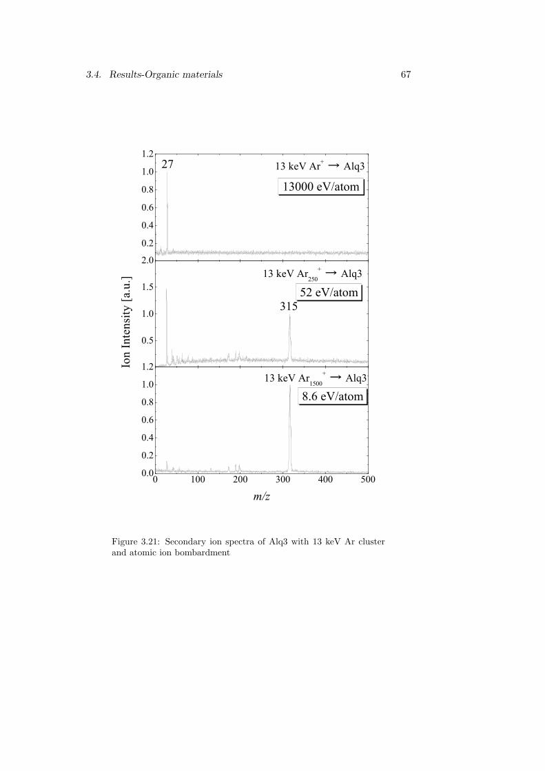
3.4. Results-Organic materials 67
0.2
0.4
0.6
0.8
1.0
1.2
0.5
1.0
1.5
2.0
0 100 200 300 400 5000.0
0.2
0.4
0.6
0.8
1.0
1.2
27
Ion
Inte
nsity
[a.u
.]
315
m/z
13 keV Ar+ Alq3
13000 eV/atom
13 keV Ar250
+ Alq3
52 eV/atom
13 keV Ar1500
+ Alq3
8.6 eV/atom
Figure 3.21: Secondary ion spectra of Alq3 with 13 keV Ar clusterand atomic ion bombardment


Chapter 4
Surface damage with GCIB
4.1 Low damage processing with GCIB irradia-tion
When GCIB bombards a surface with an energy per atom less than a few
hundred eV/atom, the high-density energy deposition induces various ir-
radiation effects. One of the characteristic irradiation effects caused by
high-density energy deposition is enhancement of chemical reactivity, and
for instance, a well-oxidized and smooth film can be formed by O2 GCIB-
assisted deposition at room temperature 8, 64).
Figure 4.1 shows the X-ray reflectometry (XRR spectra) of the Si surface
before and after ion irradiation with 20 keV O2. The average O2 cluster
size was 1500 molecules, and the irradiation dose was 1 × 10¹⁶ ions/cm2.
The thickness, density and roughness of each film were investigated by
XRR with CuKα radiation on a computer-controlled reflectometer (Rigaku
ATX. Osaka). The thickness of the oxidized films was calculated by the
wavelength of the XRR spectra curve.
The oxidized film formed on the Si substrate before irradiation was
not dense, and its wavelength was very long. On the other hand, a thick
oxidized layer was formed by O2 cluster ion irradiation, and the XRR spec-
trum was far from that of before irradiation. The estimated oxidized film
thickness was about 12 nm. The blue line represents the surface state ir-
radiated by O2 molecular ions and there was little difference between the
XRR spectra before and after O2 molecular ion irradiation. It was thus
found that ion irradiation with O2 cluster considerably enhances surface
69

70 Chapter 4. Surface damage with GCIB
0.0 0.5 1.0 1.5 2.010-6
10-5
10-4
10-3
10-2
10-1
100
In
tens
ity (a
.u)
(degree)
before irradiation 20 keV, O
2 cluster ion
20 keV, O2 atomic ion
Figure 4.1: XRR spectra of the Si surface before and after O2 ionbeam irradiation the dose of 1 × 10¹⁶ ioss/cm2.
oxidation compared to O2 molecular ion.
When a GCIB bombards a surface, numerous surface atoms are ener-
gized and excited, and even the nonreactive GCIB excites the target surface
and enhances the chemical reactions between target atoms and the gaseous
atmosphere. The target surface would be oxidized by O2 cluster ions both
directly and indirectly. Direct oxidation is the reaction of O2 cluster ions
with the target surface, and indirect oxidation is the reaction of atmospheric
O2 gas with the target surface activated by the cluster ion irradiation. By
contrast, only indirect oxidation occurs with Ar GCIB bombardment in O2
atmosphere. The reactive probability for the direct reaction with O2 cluster
should be higher than for the indirect reaction because the energy of the
constituent of O2 cluster ion is higher than that of atmospheric O2 gas.
Figure 4.2 shows the XRR spectra of the Si surface irradiated by 20 keV
Ar cluster ion in O2 atmosphere of 6.5 × 10⁻³ Pa (a) and (b) O2 cluster
ions. The irradiation dose of ion beam was 1 × 10¹⁶ ions/cm2, in both
cases and average cluster size of Ar cluster was 2000 atoms. The solid and
dotted lines in Fig. 4.2 are, respectively, the experimental and simulated
XRR spectra. The estimated thickness of the SiO2 films formed by ion
4.1. Low damage processing with GCIB irradiation 71
irradiation with Ar and O2 clusters was 15 and 12 nm, respectively.
Figure 4.3 shows secondary ion spectra of the Si target after oxidation
by irradiation with (a) 20 keV Ar cluster ion irradiation in O2 atmosphere of
6.5 × 10⁻³ Pa, and (b) 15 keV O2 cluster ion. The secondary ions emitted
from the Si surface were measured using a quadrupole mass spectrometer
(ANELVA AQA-360). Their intensity was normalized to the intensity of
Si+. The SiO+/Si+ intensity ratio obtained from the Si samples oxidized by
either irradiation with Ar cluster ion in O2 atmosphere or O2 cluster ion was
similar. This means that is, the oxygen density of the surface oxidized by
either Ar or O2 cluster ion irradiation can be considered to be roughly the
same and the Si surface was sufficiently excited for the oxidation reaction
to occur by irradiation with the nonreactive cluster ion.
Figure 4.4 shows the variation in SiO+ intensity with increasing oxygen
partial pressure (Po) during Ar cluster ion irradiation. The SiO+ intensity
increased linearly with Po below 4 × 10⁻³ Pa, and remained constant with
increasing Po above 4 × 10⁻³ Pa. As the incident energy in this experiment
was fixed at 20 keV, the excited and mixed volume on the surface by Ar
cluster ion irradiation is expected to be kept constant. This correlation of
the oxidation on O2 partial pressure could be explained as follows.
(i) For the low Po range (Po ≤ 4 × 10⁻³ Pa), the Si surface was excited
and the top layer was mixed with cluster ion irradiation, but has not ox-
idized sufficiently because insufficient amounts of oxygen were supplied to
the excited surface. Thus the SiO+ intensity was proportional to Po.
(ii) In the higher Po range (Po ≥ 4 × 10⁻³ Pa) the Si surface was
excited and the top layer that was mixed with cluster ion irradiation was
fully oxidized by sufficient amounts of oxygen. Further additon of oxygen
resulted only in excess atmosphere O2, and thus the SiO+ intensity became
independent of Po.
These experimental results indicate that the GCIB irradiation strongly
affected the solid surface, and with 20 keV GCIB the affected depth was
more than 10 nm. In other words, the surface structure was damaged more
than 10 nm by 20 keV cluster ion irradiation, and this was much deeper than
the penetration depth of an Ar atom with 10 eV, which is about 0.4nm. Of
course, this irradiation effect of GCIB mainly depends on incident cluster
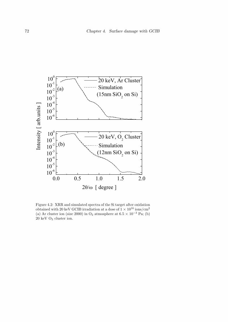
72 Chapter 4. Surface damage with GCIB
0.0 0.5 1.0 1.5 2.010-610-510-410-310-210-1100
10-610-510-410-310-210-1100
2 [ degree ]
20 keV, O2 Cluster
Simulation (12nm SiO
2 on Si)
20 keV, Ar Cluster Simulation
(15nm SiO2 on Si)
(b)
Inte
nsity
[ ar
b.un
its ]
(a)
Figure 4.2: XRR and simulated spectra of the Si target after oxidationobtained with 20 keV GCIB irradiation at a dose of 1 × 10¹⁶ ions/cm2
(a) Ar cluster ion (size 2000) in O2 atmosphere at 6.5 × 10⁻³ Pa; (b)20 keV O2 cluster ion.

4.1. Low damage processing with GCIB irradiation 73
20 30 40 500
1
2
0
1
2
15 keV, O2 Cluster
SiO+
SiOH+Si+In
tens
ity [
arb.
uni
ts ]
m/z
(b)
SiO+
SiOH+
Si+
(a) 20 keV, Ar Cluster
Figure 4.3: Secondary ion spectra of the Si target after oxidationobtained under irradiation with (a)20 keV Ar cluster ion irradiationin O2 atmosphere at 6.5 × 10⁻³ Pa, and (b) 15 keV O2 cluster ion.
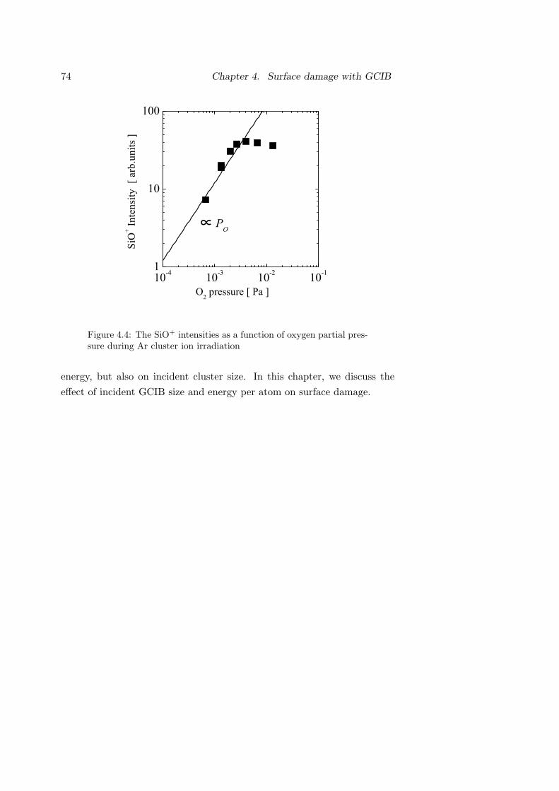
74 Chapter 4. Surface damage with GCIB
10-4 10-3 10-2 10-11
10
100
SiO
+ Inte
nsity
[ a
rb.u
nits
]
O2 pressure [ Pa ]
PO
Figure 4.4: The SiO+ intensities as a function of oxygen partial pres-sure during Ar cluster ion irradiation
energy, but also on incident cluster size. In this chapter, we discuss the
effect of incident GCIB size and energy per atom on surface damage.

4.2. Surface damage-Si target 75
4.2 Surface damage-Si target
In this part if the work, crystalline Si (100) substrates were irradiated with
Ar cluster ion beam and the thickness of the damaged surface layer was
evaluated. The incident energy of cluster ion beam was in the range of
5-20 keV. The irradiation apparatus and size selection methods were the
same as detailed in Ch. 2, and Ar GCIB irradiation was carried out at
normal incidence. The Si target was rastered for uniform irradiation and
the irradiated area was 4 mm × 6 mm. The incident cluster size was in the
range 500-16000, and the ion dose was 1 × 10¹³ ions/cm2.
The damaged layer thickness caused by irradiation of the Si substrate
was characterized by ex situ ellipsometry measurements. The two optical
parameters, the intensity ratio (Ψ) and phase difference (∆) of the p and
s waves can be measured at one laser wavelength and light incident an-
gle. The ellipsometric parameters are related to the changes in amplitude
and phase of the reflected polarized light. The thickness of the oxide and
amorphous layers caused by various sizes and energies of cluster ions can be
determined by using a two layer model. An increase in Ψ means increase in
the amorphous layer thickness and a decrease in ∆ means an increase in the
oxide layer thickness. The total damaged layer thickness was defined as the
sum of the amorphous and oxide layer thicknesses. The laser wavelength
was 635 nm and the light incident angle was 75 degree.
Figure 4.5 presents Ψ and ∆ plots after size-selected 10 keV Ar cluster
ion irradiation on the Si substrate. The red and black lines represent the
thickness of the oxide and amorphous layer (15 A/line), respectively. Before
cluster ion beam irradiation, the oxide layer thickness of the Si substrate
was about 3 nm, and there was no amorphous layer. The surface damage
with non-size-selected GCIB is shown as a red square, for comparison with
size-selected cluster ions. The damaged layer thickness with non-selected
cluster ion was similar to that with Ar1000 bombardment, although the
mean size of the non-size-selected cluster was about 1500, indicating that
the surface damage is more affected by small clusters than by large ones.
The oxide layer thickness decreased with increasing incident cluster size.
On the other hand, the amorphous layer thickness has maximum value at

76 Chapter 4. Surface damage with GCIB
0 2 4 6 8 10100
120
140
160
180
200
Bare before size selection(15,0)
(0,0)
(0,15)
amorphous layer
oxide layer
Ar500
Ar1000
Ar2000Ar4000
Ar8000
Figure 4.5: Ψ and ∆ plots of Si substrates by ellipsometry measure-ments after unselected and size-selected 10 keV Ar cluster ion beamirradiation with fluence of 1 × 10¹³ ions/cm2
Ar2000 bombardment. Between Ar4000 and Ar8000, there was a sudden drop
in the damaged layer thickness.
Figure 4.6 shows the effect of cluster size on the oxide (SiOx) and amor-
phous (a-Si) layer thickness with size-elected 10 keV Ar GCIB bombard-
ment. Blue triangles in the figure represent the sum of the layer thicknesses
of silicon oxide and amorphous silicon. The oxide and amorphous layer
thickness for Ar8000 and Ar16000 were about 3 and 0.2 nm, which is as large
as the native oxide on the silicon substrate. As shown, the total damaged
layer thickness with GCIB bombardment in the size range of 500-4000 was
similar, although the thickness of the a-Si layer decreased with increasing
incident cluster size, indicating that the mean depth of displacement does
not depend on both incident cluster size and energy per atom but only the
total incident energy if it is sufficiently higher than the damaging threshold
energy. On the other hand, the damage depth decreased with decreasing

4.2. Surface damage-Si target 77
1000 100000
4
8
12
16
20
Laye
r thi
ckne
ss (n
m)
cluster size (atoms)
aSi SiOx
aSi+SiOx
10 keV Ar cluster -> Si 10 1
Incident energy per atom (eV/atom)
Figure 4.6: The effect of incident cluster size on the thickness ofoxide(SiOx) and amorphous(aSi) layer on Si substrates by 10 keV ArGCIB
incident energy per atom when the value of this parameter was lower than
about 10 eV/atom, which is same behavor than for the other irradiation
effects such as sputtering and secondary ion emission. The thickness of the
damaged layer with small cluster ion bombardment was smaller than the
penetration depth with 10 keV Ar atomic ion, about 20 nm, as calculated
with TRIM. Crater-like damage remained after gas cluster bombardment
as mentioned in Ch. 2.
The sputtering yield with 10 keV Ar cluster ion was found to be of
5atoms, and the estimated crater depth of 1 nm. In MD simulation, the
damage depth depends only on the total incident cluster energy, and the
damaged depth is much deeper than the crater depth 27). The MD simula-
tion was in good agreement with the experimental data. Figure 4.7 presents
the effect of varying energy per atom on the damaged layer thickness for
5-20 keV size-selected GCIB. The damaged layer thickness was calculated
as the sum of the layer thicknesses of silicon oxide and a-Si, both of which
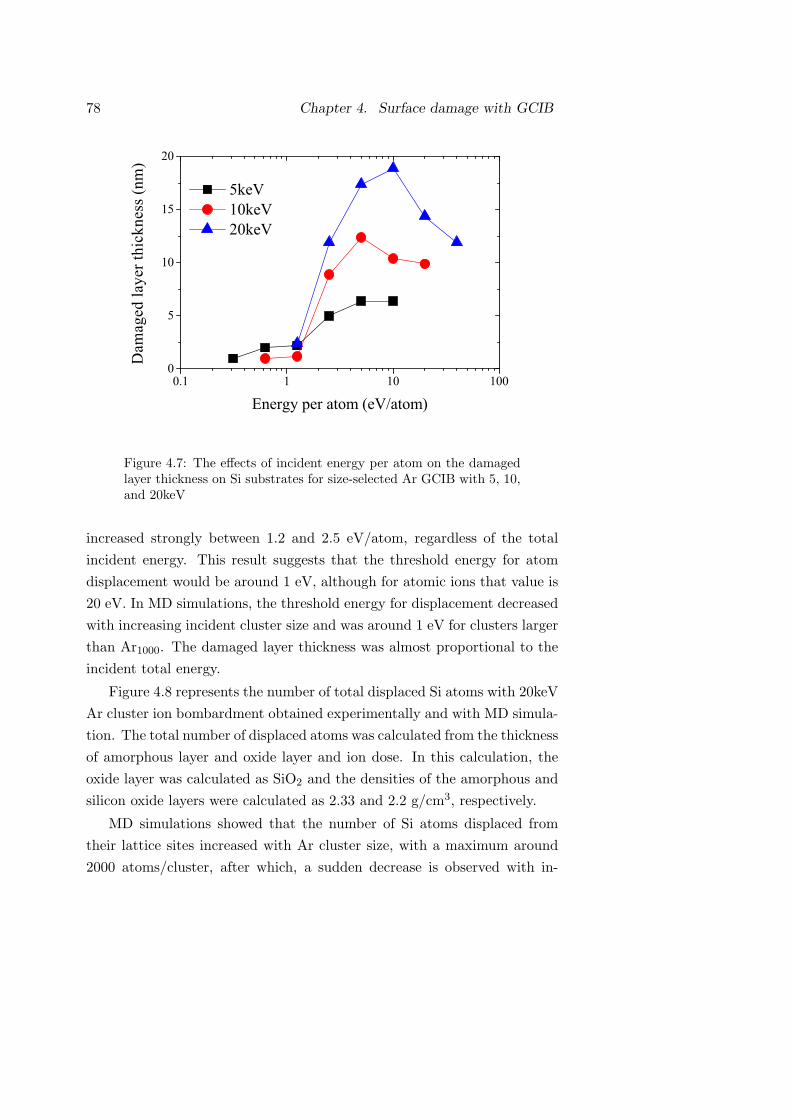
78 Chapter 4. Surface damage with GCIB
0.1 1 10 1000
5
10
15
20
5keV 10keV 20keV
Dam
aged
laye
r thi
ckne
ss (n
m)
Energy per atom (eV/atom)
Figure 4.7: The effects of incident energy per atom on the damagedlayer thickness on Si substrates for size-selected Ar GCIB with 5, 10,and 20keV
increased strongly between 1.2 and 2.5 eV/atom, regardless of the total
incident energy. This result suggests that the threshold energy for atom
displacement would be around 1 eV, although for atomic ions that value is
20 eV. In MD simulations, the threshold energy for displacement decreased
with increasing incident cluster size and was around 1 eV for clusters larger
than Ar1000. The damaged layer thickness was almost proportional to the
incident total energy.
Figure 4.8 represents the number of total displaced Si atoms with 20keV
Ar cluster ion bombardment obtained experimentally and with MD simula-
tion. The total number of displaced atoms was calculated from the thickness
of amorphous layer and oxide layer and ion dose. In this calculation, the
oxide layer was calculated as SiO2 and the densities of the amorphous and
silicon oxide layers were calculated as 2.33 and 2.2 g/cm3, respectively.
MD simulations showed that the number of Si atoms displaced from
their lattice sites increased with Ar cluster size, with a maximum around
2000 atoms/cluster, after which, a sudden decrease is observed with in-

4.2. Surface damage-Si target 79
1000 100000
50
100
150
Num
ber o
f dis
plac
ed S
i ato
ms (
atom
s/io
n)
cluster size (atoms)
Experimental
20 keV Ar cluster => Si
0
2500
5000
7500
10000
MD simulation
100 10 1
Incident energy per atom (eV/atom)
Figure 4.8: Number of total displacement atoms with 20 keV Arcluster ion bombardment 27)
creasing cluster size up to 8000 atoms/cluster. At a cluster size larger
than 20000 atoms/cluster, no atom should be displaced. The same effect
of cluster size on atom displacement was observed in experiment and MD
simulation in both the small and the large cluster regions. The number
of displaced atoms in MD simulation was about 50 times higher than in
experimental results because surface atoms were affected more than once
in this experiment. The affected area with 20 keV Ar GCIB was estimated
to be 100 nm2 in a previous report 65), and therefore each surface atom was
affected about 10 times at the dose of 1013 ions/cm2(= 0.1 ions/nm2). As
mentioned in Ch. 2, if all affected ions would be displaced from the lattice,
the true ratio between MD simulation and experiment would be about 5.
As a result, the GCIB energy per atom should be less than 2 eV/atom in
order to avoid the surface damage.
Figure 4.9 presents the number of Si atoms displaced and sputtering
yield with 20 keV Ar GCIB. The threshold energy for displacement and
sputtering was about the same, and both the sputtering and displacement
yields increased with decreasing cluster size under large cluster ion bom-

80 Chapter 4. Surface damage with GCIB
0
100
200
30010000 1000
Cluster size (atoms)
To
tal d
ispl
acem
ent S
i ato
ms (
atom
s/io
n)
Number of displaced atom
Incident energy per atom (eV/atom)
0
20
40
60
80
Number of sputtered atom
Sput
terin
g yi
eld
(ato
ms/
ion)
1 10 100
Figure 4.9: Number of total displaced atoms and sputtering yieldwith 20 keV Ar cluster ion bombardment
0.0
0.2
0.4
0.6
0.810000 1000 100
Cluster size (atoms)
Incident energy per atom (eV/atom)
Sput
terin
g pr
obab
ilty
[a.u
.]
1 10 100
20 keV Ar cluster -> Si
0.000
0.002
0.004
0.006
0.008
0.010
0.012
Ar atom(TRIM)
Figure 4.10: The sputtering probability of displaced Si with 20 keVAr cluster ion bombardment

4.2. Surface damage-Si target 81
bardment. The sputtering yield continued to increase with decreasing inci-
dent cluster size under small cluster, although the displacement efficiency
was saturated. The ratio of the number of sputtered atoms to that of dis-
placed atoms under 20 keV GCIB of varying energy were shown in Fig.4.10.
This value reflects the sputtering probability for a displaced atom. Red
dotted line represents that of Ar atom calculated in TRIM. As shown, the
sputtering probability decreased with increasing incident size. The energy
of atoms displaced with cluster ions with high energy per atom would be
higher than that of clusters with low energy-per-atom, and more particles
would be ejected from the surface.

82 Chapter 4. Surface damage with GCIB
4.3 Surface damage-Organic materials
The surface damage with ion beam irradiation is a more serious problem in
organic materials. Depth profiling with secondary ion mass spectrometry
has become the most powerful interface analysis method for these nanos-
tructures, and there is an increasing need for in-depth analysis with resolu-
tion of a few nanometer scale without damage to the underlying structure.
However, as mentioned in the previous chapter, irradiation with atomic
ions or small cluster ion beams at keV energies causes significant chemical
damage accumulation on organic compound targets 66) because of the large
energy transfer, deep penetration depth and low sputtering rate. Low en-
ergy (∼200 eV) reactive atomic ion beams, such as O+ and Cs+ have been
used to avoid damage accumulation during irradiation 67, 68), but the sput-
tering rates of these beams are extremely low. GCIB has been reported to
solve the problem of damage to biomolecules caused by incident ions 69, 70).
Figure 4.11 (a) presents the mass spectra of positively charged secondary
ions emitted from a leucine (C6H13NO2, 131 u) film with 8 keV Ar500,
which protonated leucine molecular ions and characteristic fragment ions
were observed. Leucine films (about 4 µm-thick) were prepared on a Si
substrate by evaporation. The secondary ion spectra of leucine films after
Ar atomic ion and Ar cluster ion irradiation are shown in Figure 4.11 (b)
and (c), respectively. The dose was 2 × 10¹⁵ ions/cm2 and the etching
depth was 400 nm and 1.7 µm, respectively. Large ions such as m/z = 132
and 86 were not observed after atomic ion bombardment because of damage
accumulation. In contrast, the secondary ion spectra from before and after
Ar cluster ion irradiation were completely similar. These results show that
the leucine film was only a little damaged by Ar cluster ion irradiation
despite its high sputtering yield. This indicates that large cluster ions can
sputter leucine molecules with little damage, or that sputtering yields of
large cluster ions are as large as the volume of damaged leucine molecules
by irradiation.
To investigate the surface damage more precisely, we observed the sec-
ondary ions obtained with atomic primary ion irradiation in the energy
range of MeV. When a MeV ion strikes a solid surface, it penetrates the

4.3. Surface damage-Organic materials 83
0 50 100 150
(b) after etching (10 keV Ar atomic ion, 400 nm)
(a) before etching
Se
cond
ary
ion
inte
nsity
[a.u
.]
(c) after etching (10 keV Ar cluster ion, 1700 nm)
m/z
[Leu+H]+
Figure 4.11: Secondary ion spectra of leucine (a) before, after 10 keVAr (b) atomic ion and (c) cluster ion; the dose was 2 × 10¹⁵ ions/cm2
84 Chapter 4. Surface damage with GCIB
surface and loses energy in a cylindrical region with intense ionizations and
excitations due to direct Coulomb interactions, because the stopping power
of a MeV ion is mostly due to the interaction with electrons in the target
atoms. The high-energy electrons produce new generations of low-energy
secondary electrons, and large molecules are ejected from the surface un-
der action of these secondary electrons 71, 72). Figure 4.12 (a) presents the
mass spectra of positively charged secondary ions emitted from the Alq3
(C27H18AlN3O3, 459.4 u) film with 6 MeV Cu4+. Before etching, Alq2
(m/z = 315) and Alq2+Al (m/z = 342) were observed with strong inten-
sity. The mass spectra from Alq3 films irradiated with 10 keV Ar atomic
ion and cluster ion are shown in Fig. 4.12 (b, c). The dose was 1 × 10¹⁵
ions/cm2 and etching depth was 20 nm and 250 nm, respectively. After
etching with atomic ions, no molecules were ejected from the Alq3 surface
with 6 MeV Cu4+ bombardment, although the etching depth was only 20
nm. On the other hand, a perfectly unchanged spectrum was detected from
the Alq3 surface etched with Ar cluster ions. Under irradiation with atomic
and small cluster ion such as C60, it has been difficult to sputter and analyze
Alq3 continuously because the organic particles are sputtered selectively by
energetic ion bombardment. In the case of Alq3, the target surface would
be covered by the remaining Al after a few nm sputtering 73, 74). However,
we can offer a continuous analysis such as in-depth analysis by using GCIB,
because no damage was accumulated on the surface after etching.
Figure 4.13 represents the Alq2+ ion intensity from Alq3 thin films
after etching with 10 keV Ar cluster and atomic ion bombardment. The
Alq2+ ion intensity did not decrease after etching with Ar cluster ion, but
decreased drastically with increasing etching depth with Ar atomic ion,
and only 20 % of initial intensity was detected after 1 nm etching. The
calculated damaged cross-section with 10 keV Ar cluster ion was about 3
× 10−14 cm2, i.e. one order of magnitude smaller than that with 10 keV
Ar atomic ions.
To investigate the damage accumulation, secondary ion intensity of var-
ious organic films were measured by using the depth profiling technique. In
this method, the surface is etched uniformly by Ar cluster ion beam irradi-
ation between each SIMS measurement. We used arginine (C6H14N4O2,m

4.3. Surface damage-Organic materials 85
0
50000
100000
150000
0
50000
100000
150000
0 100 200 300 400 500
0
50000
100000
150000(b)
(a)
(c)
before etching
after etching (10 keV Ar atomic ion, 20nm)
after etching (10 keV Ar cluster ion, 250nm)
Seco
ndar
y io
n in
tens
ity [a
.u.]
m/z
Figure 4.12: Secondary ion spectra of Alq3 (a) before, after bombard-ment with 10 keV Ar (b) atomic ion and (c) cluster ion; the dose was1 × 1014 ions/cm2

86 Chapter 4. Surface damage with GCIB
Figure 4.13: Secondary ion intensity of Alq2+ with 10 keV Ar clusterand atomic ion.

4.3. Surface damage-Organic materials 87
= 174u), polycarbonate (C16H14O3, PC, m = 254u) and C60 (m = 720u) in
this study. The arginine film was the same as the sample in Ch. 3. PC and
C60 were purchased from Nacalai Tesque Inc. (Kyoto, Japan) and Sigma
Aldrich Inc. (St. Louis, MO, SA), respectively. The PC films were prepared
by spin-casting and the C60 films were prepared by evaporation methods
on Si substrate. The thickness of the arginine, PC and C60 films was 350,
70 and 50 nm, respectively. The targets were at ambient temperature.
Figure 4.14 presents the intensities of characteristic secondary ion from
arginine(m/z = 175), PC(m/z = 135) and C60(m/z = 720) as a function
of etched film depth (lower horizontal axis) and Irradiation dose (upper
horizontal axis). The secondary ion intensity was independent of the inci-
dent ion fluence until the film was etched completely, indicating that there
was no surface accumulation and that the surface damage only depended
on the incident cluster conditions. Figure 4.14 presents C1s and O1s X-ray
photoelectron spectra (XPS) spectra of PMMA samples before and after
Ar cluster ion beam irradiation. The molecular structure of PMMA was
shown in Fig 3.16. The mean cluster size was 2000. The C1s peak can
be deconvoluted into three components, and the O1s peak can be decon-
voluted into two components. After etching with 20 keV Ar cluster ions,
the C1s and O1s spectra changed and the peak intensity of O-C=O, C=O,
C=O and C-O-C decreased slightly compared to the unirradiated PMMA
sample. After etching with 5 and 10 keV Ar cluster ions, the locations
and intensities of the C1s and O1s peaks alomost completely agreed with
those of unirradiated PMMA sample 75). This results agree with the re-
sults of SIMS spectra, shown in Ch. 3. Therefore, to avoid damage during
irradiation the incident energy per atom should be lower than 5 eV/atom.

88 Chapter 4. Surface damage with GCIB
0 100 200 300 400
10
100
1000
0 1x10¹⁵ 2x10¹⁵ 3x10¹⁵ 4x10¹⁵
0 20 40 60 80 100
10
100
1000
0 1x10¹⁴ 2x10¹⁴ 3x10¹⁴ 4x10¹⁴ 5x10¹⁴
0 20 40 60 80 100
10
100
1000
0 1x10¹⁴ 2x10¹⁴ 3x10¹⁴ 4x10¹⁴ 5x10¹⁴
Irradiation dose (ions/cm2)
10 keV Ar cluster ion => Arginine
m/z = 175
m/z = 135
Seco
ndar
y io
n in
tens
ity [a
.u,]
10 keV Ar cluster ion => PC
m/z = 720
Etching depth (nm)
10 keV Ar cluster ion => C60
Figure 4.14: Secondary ion intensity of organic films after etching by10 keV Ar cluster ion.

4.3. Surface damage-Organic materials 89
294 292 290 288 286 284 282 280 278O-C=OC=O
Intensity [ arb. unit ]
Binding energy [ eV ]
As receivedAr cluster →→→→ PMMA 20 keV 10 keV 5 keVC1sC-C,C-H
542 540 538 536 534 532 530 528 526C=O C-O-C
Binding energy [ eV ]
As receivedAr cluster →→→→ PMMA 20 keV 10 keV 5 keVO1s
Figure 4.15: C1s and O1s XPS spectra of PMMA samples before andafter irradiation with 5-20 keV Ar cluster ion.

Chapter 5
Surface morphology with GCIB
5.1 Surface smoothing with GCIB irradiation
When a large gas cluster ion bombards a surface, multiple collisions occur in
the near surface region and a crater-like damage forms on the surface. Fol-
lowing the impact, surface atoms are displaced in a lateral direction along
the surface, and some atoms are sputtered. As mentioned in Ch. 4, the vol-
ume of displaced atoms would be a few hundred nm3 under 10 keV cluster
ion bombardment. Therefore, surface grain structures are rapidly removed
and the rough surface becomes smooth under GCIB irradiation 76, 77). In
conventional atomic ion bombardment, the ion beam penetrates the sur-
face and causes a small hillock. To avoid roughening the surface, the ion
beam energies need to be in the range of a few hundreds of eV. However,
it is difficult to produce low-energy ion beams at high intensity because of
their space-charge effects. On the other hand, with GCIB surface smooth-
ing without any scratches has been reported for various inorganic targets
such as Cu and CVD diamond 78). Dry polishing and smoothing of hard or
unreactive materials are feasible by using GCIB. Moreover, because of the
low mass-to-charge ratio a large beam current can be produced. Therefore,
GCIB has been proposed for surface smoothing applications 79, 80, 81). Of
course, the target surface would be different after fast or slow cluster ion
irradiation,so that optimum condition has to be selected to apply GCIB
most effectively. In this chapter, we discuss the incident cluster size and
energy per atom effects on surface morphology for GCIB irradiation.
91
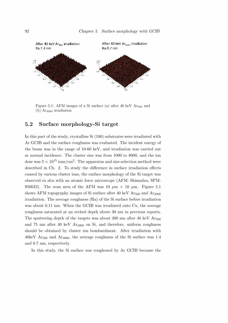
92 Chapter 5. Surface morphology with GCIBAfter 40 keV Ar500 irradiationRa:1.4 nm After 40 keV Ar4000 irradiationRa:0.7 nm
Figure 5.1: AFM images of a Si surface (a) after 40 keV Ar500 and(b) Ar4000 irradiation
5.2 Surface morphology-Si target
In this part of the study, crystalline Si (100) substrates were irradiated with
Ar GCIB and the surface roughness was evaluated. The incident energy of
the beam was in the range of 10-60 keV, and irradiation was carried out
at normal incidence. The cluster size was from 1000 to 8000, and the ion
dose was 5 × 10¹⁵ ions/cm2. The apparatus and size-selection method were
described in Ch. 2. To study the difference in surface irradiation effects
caused by various cluster ions, the surface morphology of the Si target was
observed ex situ with an atomic force microscope (AFM: Shimadzu, SPM-
9500J2). The scan area of the AFM was 10 µm × 10 µm. Figure 5.1
shows AFM topography images of Si surface after 40 keV Ar500 and Ar4000
irradiation. The average roughness (Ra) of the Si surface before irradiation
was about 0.11 nm. When the GCIB was irradiated onto Cu, the average
roughness saturated at an etched depth above 30 nm in previous reports.
The sputtering depth of the targets was about 300 nm after 40 keV Ar500
and 75 nm after 40 keV Ar4000 on Si, and therefore, uniform roughness
should be obtained by cluster ion bombardment. After irradiation with
40keV Ar500 and Ar4000, the average roughness of the Si surface was 1.4
and 0.7 nm, respectively.
In this study, the Si surface was roughened by Ar GCIB because the
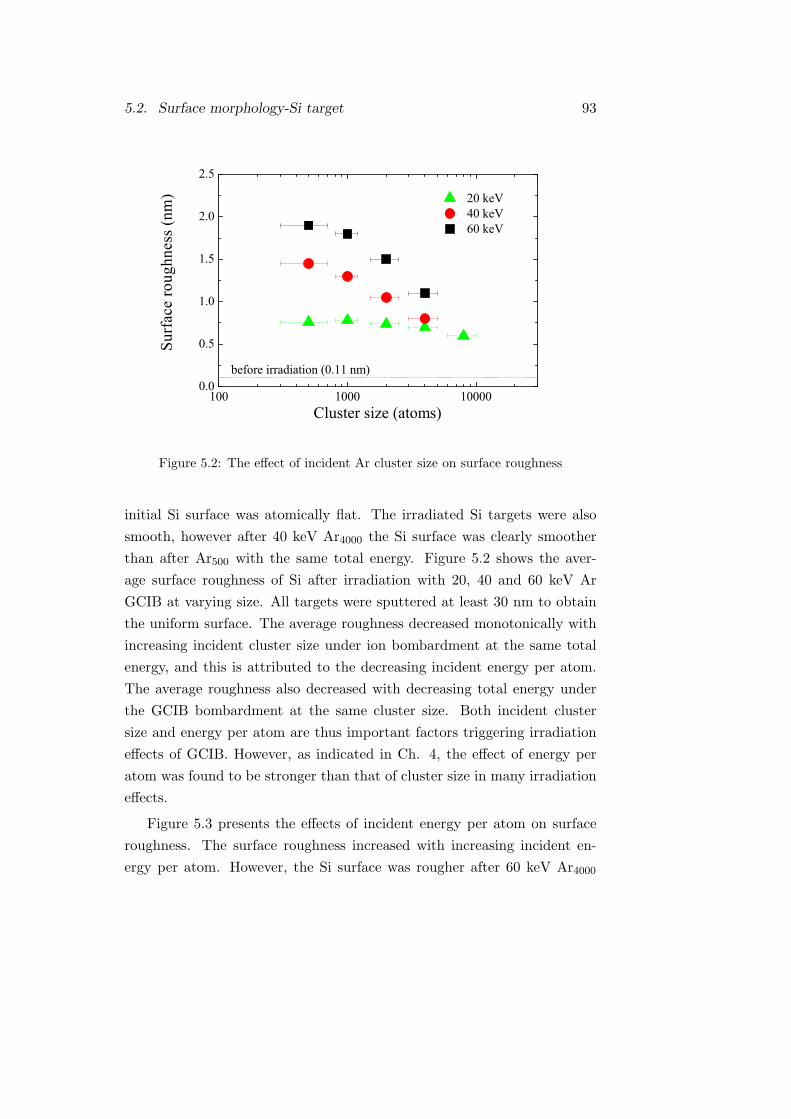
5.2. Surface morphology-Si target 93
100 1000 100000.0
0.5
1.0
1.5
2.0
2.5
20 keV 40 keV 60 keV
Cluster size (atoms)
Surf
ace
roug
hnes
s (nm
)
before irradiation (0.11 nm)
Figure 5.2: The effect of incident Ar cluster size on surface roughness
initial Si surface was atomically flat. The irradiated Si targets were also
smooth, however after 40 keV Ar4000 the Si surface was clearly smoother
than after Ar500 with the same total energy. Figure 5.2 shows the aver-
age surface roughness of Si after irradiation with 20, 40 and 60 keV Ar
GCIB at varying size. All targets were sputtered at least 30 nm to obtain
the uniform surface. The average roughness decreased monotonically with
increasing incident cluster size under ion bombardment at the same total
energy, and this is attributed to the decreasing incident energy per atom.
The average roughness also decreased with decreasing total energy under
the GCIB bombardment at the same cluster size. Both incident cluster
size and energy per atom are thus important factors triggering irradiation
effects of GCIB. However, as indicated in Ch. 4, the effect of energy per
atom was found to be stronger than that of cluster size in many irradiation
effects.
Figure 5.3 presents the effects of incident energy per atom on surface
roughness. The surface roughness increased with increasing incident en-
ergy per atom. However, the Si surface was rougher after 60 keV Ar4000
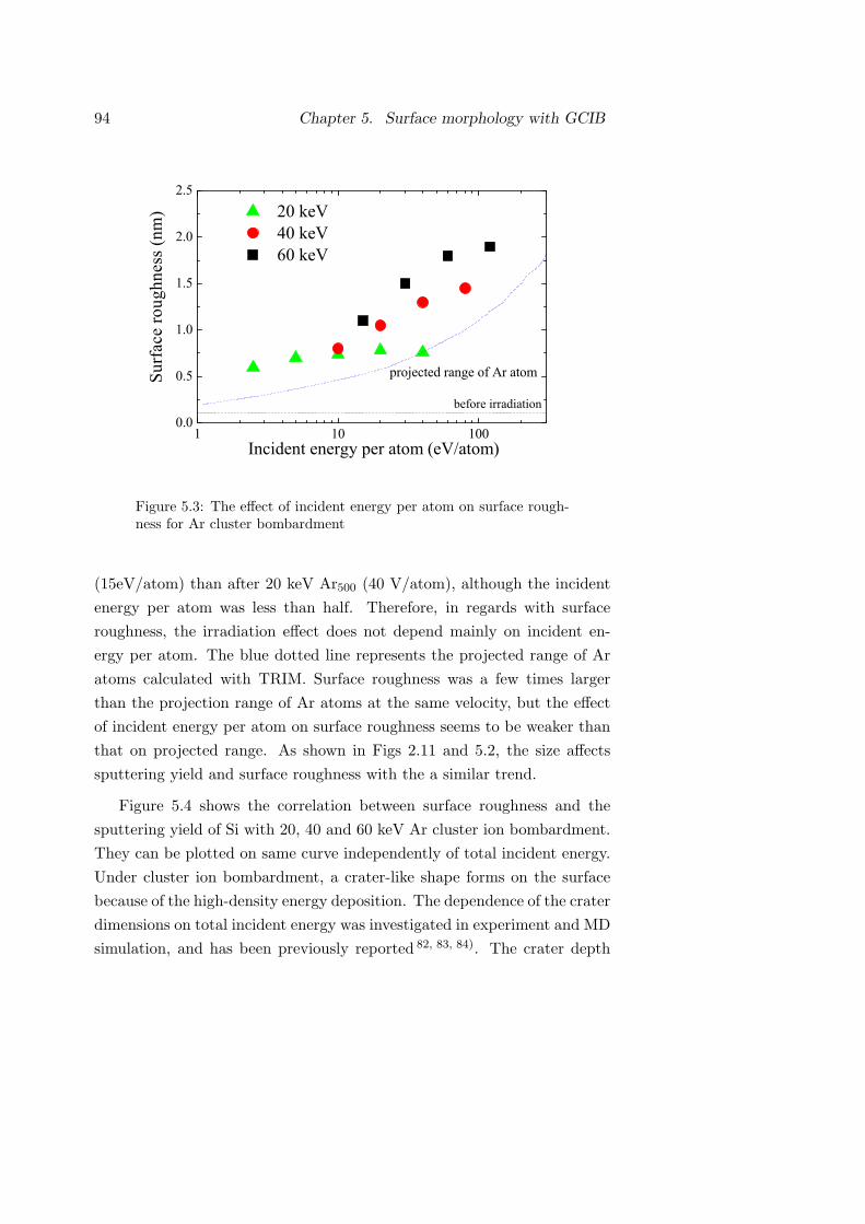
94 Chapter 5. Surface morphology with GCIB
1 10 1000.0
0.5
1.0
1.5
2.0
2.5 20 keV 40 keV 60 keV
Incident energy per atom (eV/atom)
Surf
ace
roug
hnes
s (nm
)
before irradiation
projected range of Ar atom
Figure 5.3: The effect of incident energy per atom on surface rough-ness for Ar cluster bombardment
(15eV/atom) than after 20 keV Ar500 (40 V/atom), although the incident
energy per atom was less than half. Therefore, in regards with surface
roughness, the irradiation effect does not depend mainly on incident en-
ergy per atom. The blue dotted line represents the projected range of Ar
atoms calculated with TRIM. Surface roughness was a few times larger
than the projection range of Ar atoms at the same velocity, but the effect
of incident energy per atom on surface roughness seems to be weaker than
that on projected range. As shown in Figs 2.11 and 5.2, the size affects
sputtering yield and surface roughness with the a similar trend.
Figure 5.4 shows the correlation between surface roughness and the
sputtering yield of Si with 20, 40 and 60 keV Ar cluster ion bombardment.
They can be plotted on same curve independently of total incident energy.
Under cluster ion bombardment, a crater-like shape forms on the surface
because of the high-density energy deposition. The dependence of the crater
dimensions on total incident energy was investigated in experiment and MD
simulation, and has been previously reported 82, 83, 84). The crater depth

5.2. Surface morphology-Si target 95
0 100 200 300 400 500 6000.0
0.5
1.0
1.5
2.0
2.5
60 keV 40 keV 20 keV
Sputtering yield (atoms/ion)
before irradiationSurf
ace
roug
hnes
s (nm
)
Y1/3
Figure 5.4: The effect of sputtering yield on surface roughness for Arcluster bombardment
was found to be proportional to the cubic root of the total incident energy.
The red dotted line presents the crater depth calculated from the Si sput-
tering yield and density (2.33 g/cm3), and was in good agreement with the
experimental data if the sputtering yield was lower than 300 atoms/ion.
On the other hand, under high sputtering yield conditions, which includes
60 keV Ar500 and Ar1000, the proportionality seems to be lost. The results
under these conditions suggest that hemispherical craters were formed on
the Si surface with GCIB, and the crater shape reflects the surface rough-
ness. The crater shape remained unchanged for sputtering yield lower than
300 atoms/ion, and became vertically elongated with increasing sputtering
yield above this value. In other words, this study indicates that small and
fast cluster bombardment forms deep craters. The sputtering probability
of fast clusters was higher than that of slow clusters, as mentioned in Ch.
4, and this means that the incident cluster conditions are reflected in the
crater shape under small and fast cluster bombardment.
Figure 5.5 presents the correlations between surface roughness and sput-

96 Chapter 5. Surface morphology with GCIB
0 200 400 600 800 10000.0
0.5
1.0
1.5
2.0
Ar SF
6
Sputtering yield (atoms/ion)
Y1/3
Surf
ace
roug
hnes
s (nm
)
Figure 5.5: The effect of sputtering yield on surface roughness for Arand SF6 cluster bombardment
tering yield with Ar and SF6 cluster ion bombardment. The energy of the
SF6 cluster was 20 keV, and the mean cluster sizes were 600, 1500 and
3000 molecules/ion. SF6 cluster is a reactive cluster ion, and the Si sput-
tering yield with 20 keV SF6 cluster was more than 10 times higher than
that with 20 keV Ar cluster ion. The black and blue dots indicate the
results for Ar and SF6 cluster ions, respectively. The surface roughening
processes with Ar cluster ion and SF6 cluster ion were completely different.
For example, Si surface roughness after irradiation with 20 keV (SF6)3000
and 60 keV Ar1000 was about 0.7 and 1.7 nm, although the Si sputtering
yield was about the same (∼400 atoms/ion). For ion bombardment with
the same velocity, after irradiation with 20 keV (SF6)600 (0.23 eV/u) and
Ar2000 (0.25 eV/u) the surface roughness values were about 1.5 and 0.7nm,
respectively. These results suggests that crater shapes obtained with Ar
and SF6 clusters is different.
Figure 5.6 presents a model of surface morphology with nonreactive
and reactive cluster ion bombardment. Under nonreactive cluster ion bom-

5.2. Surface morphology-Si target 97
Figure 5.6: The model of sputtering for non-reactive(Ar) andreactive(SF6) cluster bombardment
bardment, hemispherical crater damage has formed physically. The shape
of this crater was roughly independent of incident cluster conditions, and
the volume increased with increasing incident cluster size and energy per
atom. The surface roughness after irradiation with nonreactive cluster ion
was proportional to the crater depth, and therefore proportional to the
cube root of the sputtering yield. Under reactive cluster ion bombardment,
hemispherical crater damage is formed physically in the first stage. After
the physical sputtering, the reactive constituent remains on the target sur-
face and forms a chemical compound with the excited atoms. Finally, the
chemical compound evaporates and leaves the surface. In MD simulation,
the time scales of physical and chemical sputtering were reported to be a
few ps and a few 10 ps, respectively 85). In the experiment, the diameter
affected by a 20 keV Ar cluster was about 10 nm 86). Under such nonre-
active bombardment, less than 1 % of affected atoms are sputtered. For
instance, the volume of displaced atoms with 20 keV Ar1000 was 140 nm3
per incident ion. Meanwhile, the volume of sputtered matteris of 0.7 nm3,
implying that the sputtering probability is only 0.5 %. The sputtered Si
volume with 20 keV (SF6)3000 was 8 nm3, which means no more than one
layer of the surface craters (80 nm2). Therefore, the actual crater depth

98 Chapter 5. Surface morphology with GCIB
with nonreactive and reactive cluster ion impact was approximately the
same, whereas the sputtering yield with reactive GCIB was one order of
magnitude higher than with nonreactive GCIB.
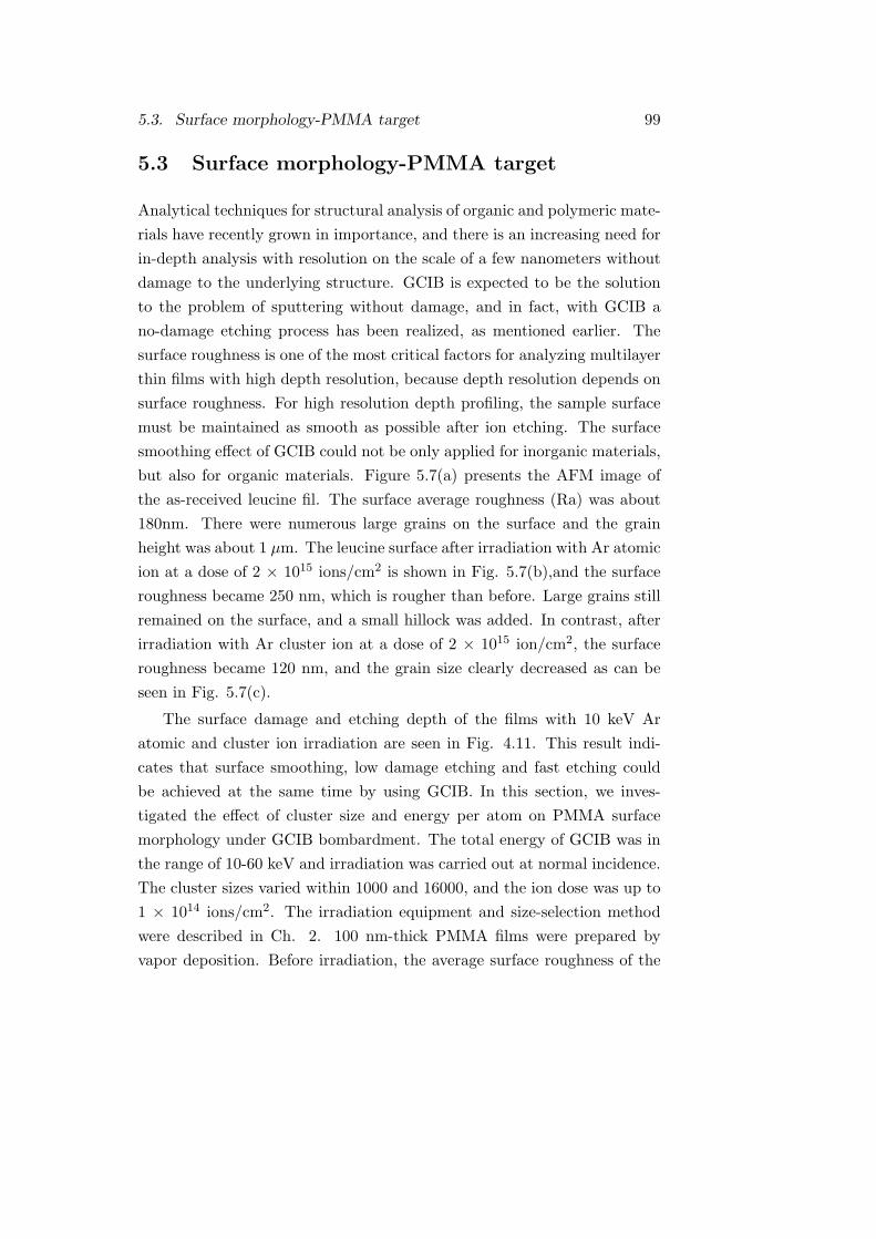
5.3. Surface morphology-PMMA target 99
5.3 Surface morphology-PMMA target
Analytical techniques for structural analysis of organic and polymeric mate-
rials have recently grown in importance, and there is an increasing need for
in-depth analysis with resolution on the scale of a few nanometers without
damage to the underlying structure. GCIB is expected to be the solution
to the problem of sputtering without damage, and in fact, with GCIB a
no-damage etching process has been realized, as mentioned earlier. The
surface roughness is one of the most critical factors for analyzing multilayer
thin films with high depth resolution, because depth resolution depends on
surface roughness. For high resolution depth profiling, the sample surface
must be maintained as smooth as possible after ion etching. The surface
smoothing effect of GCIB could not be only applied for inorganic materials,
but also for organic materials. Figure 5.7(a) presents the AFM image of
the as-received leucine fil. The surface average roughness (Ra) was about
180nm. There were numerous large grains on the surface and the grain
height was about 1 µm. The leucine surface after irradiation with Ar atomic
ion at a dose of 2 × 10¹⁵ ions/cm2 is shown in Fig. 5.7(b),and the surface
roughness became 250 nm, which is rougher than before. Large grains still
remained on the surface, and a small hillock was added. In contrast, after
irradiation with Ar cluster ion at a dose of 2 × 10¹⁵ ion/cm2, the surface
roughness became 120 nm, and the grain size clearly decreased as can be
seen in Fig. 5.7(c).
The surface damage and etching depth of the films with 10 keV Ar
atomic and cluster ion irradiation are seen in Fig. 4.11. This result indi-
cates that surface smoothing, low damage etching and fast etching could
be achieved at the same time by using GCIB. In this section, we inves-
tigated the effect of cluster size and energy per atom on PMMA surface
morphology under GCIB bombardment. The total energy of GCIB was in
the range of 10-60 keV and irradiation was carried out at normal incidence.
The cluster sizes varied within 1000 and 16000, and the ion dose was up to
1 × 10¹⁴ ions/cm2. The irradiation equipment and size-selection method
were described in Ch. 2. 100 nm-thick PMMA films were prepared by
vapor deposition. Before irradiation, the average surface roughness of the

100 Chapter 5. Surface morphology with GCIB
(a) Before irradiation
(b) After 10 keV atomic ion (c) After 10 keV cluster ionRa 180 nm
Ra 250 nm Ra 120 nmFigure 5.7: AFM images of the leucine films (a) before and afterirradiation with at a dose of 2 × 10¹⁵ ions/cm2 , 10 keV Ar (b)atomic ion and (c) cluster ion. (The scanned area is 10µm × 10 µm)
PMMA sample was about 0.22 nm.
Figure 5.8 presents AFM topography images of the PMMA samples
after irradiation with 20 keV Ar1000 and Ar16000. The etching depth of
PMMA films was 60 and 40 nm, respectively. After irradiation with the
two cluster sizes, Ar1000 and Ar16000, the PMMA surface was roughened
to 5.0 nm and 0.78 nm, respectively. Small grains were observed on both
PMMA samples, but the grain with Ar1000 was higher than with Ar16000.
Figure 5.9 shows the correlations between the surface roughness and
sputtering depth of PMMA samples under cluster ion irradiation with
20keV for sizes Ar1000, Ar4000 and Ar16000. The surface roughness increased
with increasing etching depth for each cluster ion, and saturated after 30nm
sputtering. This result agrees with the report on Cu surface smoothing with
Ar cluster ion.
Figure 5.10 shows the saturated surface roughness under 20 keV Ar
cluster ion irradiation with size between Ar1000 and Ar16000. All targets
were sputtered at least 30 nm to saturate the surface roughness. The aver-
age roughness decreased monotonically with increasing incident cluster size.
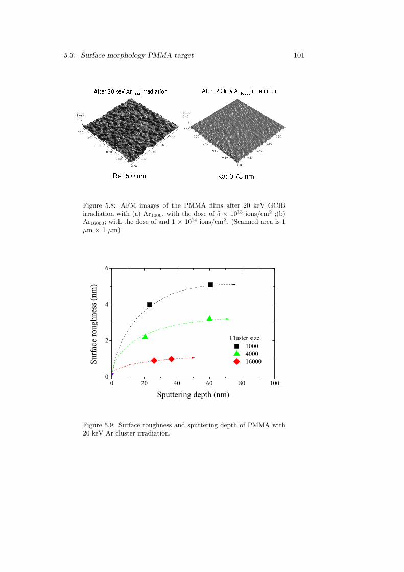
5.3. Surface morphology-PMMA target 101
Ra: 5.0 nm
After 20 keV Ar1000 irradiation
Ra: 0.78 nm
After 20 keV Ar16000 irradiation
Figure 5.8: AFM images of the PMMA films after 20 keV GCIBirradiation with (a) Ar1000, with the dose of 5 × 10¹³ ions/cm2 ;(b)Ar16000; with the dose of and 1 × 10¹⁴ ions/cm2. (Scanned area is 1µm × 1 µm)
0 20 40 60 80 1000
2
4
6
Cluster size 1000 4000 16000Su
rfac
e ro
ughn
ess (
nm)
Sputtering depth (nm)
Figure 5.9: Surface roughness and sputtering depth of PMMA with20 keV Ar cluster irradiation.
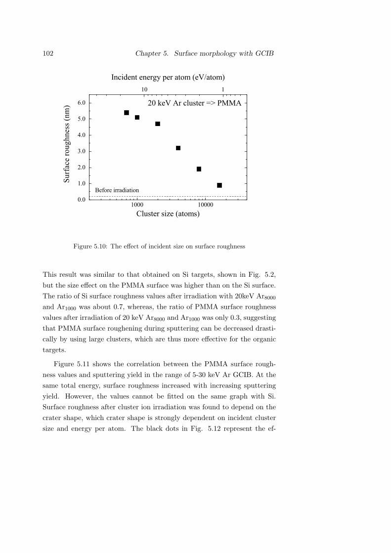
102 Chapter 5. Surface morphology with GCIB
1000 100000.0
1.0
2.0
3.0
4.0
5.0
6.0
Before irradiation
Surf
ace
roug
hnes
s (nm
)
Cluster size (atoms)
20 keV Ar cluster => PMMA
10 1
Incident energy per atom (eV/atom)
Figure 5.10: The effect of incident size on surface roughness
This result was similar to that obtained on Si targets, shown in Fig. 5.2,
but the size effect on the PMMA surface was higher than on the Si surface.
The ratio of Si surface roughness values after irradiation with 20keV Ar8000
and Ar1000 was about 0.7, whereas, the ratio of PMMA surface roughness
values after irradiation of 20 keV Ar8000 and Ar1000 was only 0.3, suggesting
that PMMA surface roughening during sputtering can be decreased drasti-
cally by using large clusters, which are thus more effective for the organic
targets.
Figure 5.11 shows the correlation between the PMMA surface rough-
ness values and sputtering yield in the range of 5-30 keV Ar GCIB. At the
same total energy, surface roughness increased with increasing sputtering
yield. However, the values cannot be fitted on the same graph with Si.
Surface roughness after cluster ion irradiation was found to depend on the
crater shape, which crater shape is strongly dependent on incident cluster
size and energy per atom. The black dots in Fig. 5.12 represent the ef-

5.3. Surface morphology-PMMA target 103
fect of incident energy per atom on surface roughness for Ar2000, and the
energy per atom is shown on the top horizontal axis. Surface roughness
increased linearly with increasing incident energy per atom. On the other
hand, the red circles in Figure 5.12 represent the effect of cluster size on
surface roughness for Ar cluster ion bombardment with 5 eV/atom, and
cluster size is presented on the bottom horizontal axis. Surface roughness
increased with 5 eV/atom small Ar cluster bombardment, and was weakly
dependent on incident cluster size under large cluster ion bombardment.
These results indicate that for an organic target the crater depth strongly
depends on the incident energy per atom. This result differs from that of Si,
and is attributed to the difference in sputtering yield. In the case of Si, the
sputtering probability was less than 1 %, and therefore the crater shape was
independent of incident cluster conditions. In the case of PMMA, the sput-
tering probability was at least 20 %, and therefore GCIB with high energy
per atom forms a deeper crater. The ion range in PMMA of an Ar atom
with 12.5 eV energy as calculated by TRIM was less than 1 nm, at which
sputtering does not occur because the binding energy between PMMA units
is of the order of a few eVs. Compared with atomic ion bombardment with
the same energy per atom, both the penetration depth and crater diameter
would increase with incident cluster size under cluster ion bombardment be-
cause of the multiple collisions occurring on the surface. The crater radius
and depth with 10 keV Ar800 bombardment were estimated to be about 2.5
and 2.9 nm from the sputtering rate and surface roughness, respectively.
The penetration depth was more than twice that observed with atomic ion
bombardment and the crater shape was hemispherical. The calculated ra-
dius for Ar800 was about 2.0 nm. This crater was bigger than the cluster,
but shallower than the cluster diameter, suggesting that under 10 keV Ar800
bombardment a part of the cluster constituent atoms penetrate the PMMA
surface, and therefore both sputtering volume and crater depth increased
as cluster size increased under small-cluster GCIB. On the other hand, the
crater radius and depth with 60 keV Ar4800 bombardment were estimated
to be about 6.8 and 6.2 nm. In this case, the crater radius was larger than
the crater depth.
Open circles in Figure 5.13 present the cubic root of the PMMA sput-

104 Chapter 5. Surface morphology with GCIB
0 200 400 600 800 1000 1200 1400
1
2
3
4
5
6
30 kV 20 kV 10 kV 5 kV
Sputtering yield (units/ion)
Surf
ace
roug
hnes
s (nm
)
Figure 5.11: Correlations between sputtering yield and surface rough-ness for Ar cluster bombardment
tering yield with Ar GCIB. As shown, the surface roughness was in good
agreement with the cubic root of the sputtering yield for sizes below Ar2400,
indicating that the crater shape with small cluster ion bombardment was
similar. However, surface roughness does not increase rapidly with GCIB
above Ar3200. Under large cluster ion bombardment, the crater shape was
wider than that with small cluster ion at constant energy per atom. As
reported from MD simulation, the crater depth with large cluster bombard-
ment obeyed the power law of total cluster energy and the power index was
about 1/3 for constant cluster size. In addition, the crater depth decreased
with increasing incident cluster size under the same-energy cluster ion.
Three models of the PMMA surface after Ar cluster ion bombardment
are shown in Figure 5.14. The parameters r and d represent the crater
radius and depth, respectively. The ratio of d/r was similar in the size
range of 800-2400. In contrast, for Ar4800 it would be smaller than with
Ar2400, suggesting that the effect of incident cluster size on crater depth was
low with large clusters, and that surface roughness strongly depends on the

5.3. Surface morphology-PMMA target 105
0 2000 4000 60000
1
2
3
4
5
6
70 5 10 15
Incident energy per atom (eV/atom)
Surf
ace
roug
hnes
s (nm
)
Cluster size (atoms)
same size (2000 atoms/ion) same velocity(5 eV/atom)
Figure 5.12: The effect of Ar cluster size and energy per atom onsurface roughness
0 800 1600 2400 3200 4000 48000.0
1.0
2.0
3.0
4.0
5.0
6.0 Surface roughness
Cluster size (atoms)
Surf
ace
roug
hnes
s (nm
)
0
5
10
15 Sputtering yield 1/3
Sput
terin
g yi
eld
1/3 (a
rb.u
nit.)
Figure 5.13: The effect of acceleration voltage on surface roughnessfor Ar cluster ion.

106 Chapter 5. Surface morphology with GCIB10 keVAr800 30 keVAr2400 60 keVAr4800
d1 r1 r2d2 d3 r3d1/r1≒d2/r2 d2/r2>d3/r3
Figure 5.14: Models of the PMMA surface after 12.5 eV/atom Arcluster ion bombardment. The crater shape with Ar800 and Ar2400was similar. the crater shape with Ar4800 had a wider opening thanthat with Ar2400.
crater depth. Therefore, the PMMA surface roughness after irradiation
with 60 keV Ar4800 was about same as with 30 keV Ar2400. The results
indicated that high sputtering yield without important roughening of the
surface is possible with large cluster ions.

Chapter 6
Summary and conclusions
In this study, we have explored the effects of cluster size and energy per
constituent on cluster interactions with the surface of Si and organic tar-
gets. GCIB has various unique irradiation effects, and it is necessary to
understand the surface physics for its effective use in various applications.
To evaluate the optimum cluster conditions, the phenomena of sputtering,
secondary ion emission, surface damaging and surface morphology were
investigated under impact of Argon GCIB at various conditions.
In the case of Si, the thickness of the damaged layer increased propor-
tionally to the total incident energy, while the sputtering and secondary ion
yields increased nonlinearly and faster than damage amount. These results
showed that the incident energy was efficiently transferred from the GCIB
to the solid surface, probably due a thermal spike occuring under cluster
bombardment. With decreasing incident energy per atom, both the dam-
aged layer thickness and sputtering yield decreased. The threshold energy
per atom for apparition of a damaged layer and for sputtering was about
1 and a few eV/atom respectively. These values are much lower than that
with atomic ions. We assume that this is the result of multiple collisions
between the cluster ion’s constituent atoms and surface atoms. On the
other hand, the threshold energy of incident cluster ion for Si+ emission
was found to be about 8 eV/atom because a certain kinetic energy is nec-
essary for the emitted particles to be ionized. It has also been found that
hemispherical craters are formed by gas cluster ion bombardment, by sur-
face roughness after cluster irradiation which unveiled topography build-up
whose features dimentions were similar to the calculated crater radius.
107
108 Chapter 6. Summary and conclusions
Under Ar GCIB bombardment of Si targets, Si secondary ion cluster
such as Si+2 and Si+3 were measured with high intensity. For example,
95 % of the total Si secondary ion counts obtained under 40 keV Ar+1100irradiation were from Si cluster ions. The intensity ratio of the Si clusters
decreased with increasing incident energy per atom. This result is in good
agreement with Si emission with laser ablation and suggests that the Si
cluster ions are emitted directly as clusters from the surface. Sputtering
yield and secondary ion yield are enhanced by cluster ion bombardment. Si
sputtering yield with 60 keV Ar+300 was about 2 atoms/ constituent atom,
which is about 10 times higher than with 0.2 keV Ar. This enhancement is
as large as that with C60 bombardment. This indicate that the enhancement
of Si sputtering yield with cluster ion bombardment is saturated at about
10.
In the case of organic targets, sputtering yield and secondary ion in-
tensity did not decrease with increasing dose after GCIB irradiation, but
they decreased rapidly under atomic ion beam. It indicates that damage
accumulation did not occur with Ar GCIB. Indeed the organic surface was
not damaged by GCIB irradiation when the incident energy per atom was
less than 5 eV/atom because it is much easier to break the van der Waals
bonding between Ar atoms (≤ 0.1 eV) than the bonding in molecules such
as C-C and C-O (≥ 2 eV). The surface roughness of irradiated organic
materials was thus strongly dependent on incident energy per atom and
weakly dependent on incident cluster size. On the other hand, the sput-
tering yield was proportional to the incident cluster size. Therefore, fast
etching without damaging and roughening are feasible with GCIB with low
energy per atom and large size.

Chapter 7
Appendix
7.1 Energy loss during transportation
Energy loss during transportation is one of the serious problems with gas
cluster ion beam irradiation. The collision frequency of gas cluster ion
beams with residual gas during transportation is two orders of magnitude
higher than that of an atomic ion beam 87) because a gas cluster is an
aggregate of thousands of atoms.
In atomic ion beam irradiation, the collision with residual gas is elastic,
and incident velocity decreases. In gas cluster ion beam irradiation, the
total energy of the cluster ion decreases after collision, but the incident
velocity does not decrease 88), indicating that the energy loss of cluster is
mainly the result of the scattering of constituent atoms. The constituent
atoms in the cluster are bound by van der Waals attraction, which is much
lower than the acceleration energy of the cluster ion, and thus cluster easily
collapse in collision with residual gas. Thus, it is necessary to reduce the
chamber pressure in cluster ion beam irradiation. However, the chamber
pressure would increase with an increase in incident cluster beam intensity
because almost all incident ions turn to residual gas after bombardment.
For example, under 1 mA of Ar1000 irradiation evacuated with a 4000liter/sec
pump, chamber pressure is about 6 × 10⁻³ Pa. It is difficult to achieve high
current intensity and good chamber pressure. It is important to study the
effect of chamber pressure for irradiation efficiency and determine the pres-
sure range under cluster ion irradiation. In this study, we investigated the
effect of varying incident energy and chamber pressure on the sputtering
109
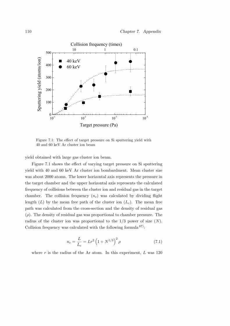
110 Chapter 7. Appendix
10-1 10-2 10-3 10-40
100
200
300
400
500
40 keV 60 keV
Sput
terin
g yi
eld
(ato
ms/
ion)
Target pressure (Pa)
10 1 0.1Collision frequency (times)
Figure 7.1: The effect of target pressure on Si sputtering yield with40 and 60 keV Ar cluster ion beam
yield obtained with large gas cluster ion beam.
Figure 7.1 shows the effect of varying target pressure on Si sputtering
yield with 40 and 60 keV Ar cluster ion bombardment. Mean cluster size
was about 2000 atoms. The lower horizontal axis represents the pressure in
the target chamber and the upper horizontal axis represents the calculated
frequency of collisions between the cluster ion and residual gas in the target
chamber. The collision frequency (nc) was calculated by dividing flight
length (L) by the mean free path of the cluster ion (Lc). The mean free
path was calculated from the cross-section and the density of residual gas
(ρ). The density of residual gas was proportional to chamber pressure. The
radius of the cluster ion was proportional to the 1/3 power of size (N).
Collision frequency was calculated with the following formula 87):
nc =L
Lc= Lr2
(1 +N1/3
)2ρ (7.1)
where r is the radius of the Ar atom. In this experiment, L was 120

7.1. Energy loss during transportation 111
mm and r was calculated as 0.19 nm. If the target chamber pressure was 2
× 10−3 Pa, the expected collision frequency would be about 1. In collisions
with residual gas, some atoms in the cluster scatter and the total energy
of the cluster ion decreases. Then, the sputtering yield after collision (Yc)
can be shown as follows:
Yc(E) = Y (knE) (7.2)
where Y (E) is calcluted by the equation (2.4) and k is the ratio of
cluster energy before and after the collision. Dotted line in Figure 7.1
represents the calculated Yc(E) from the equation (7.2). For 40 and 60 keV
ion bombardment, the k were 0.95 ± 0.01 and 0.96 ± 0.01, respectively.
The cluster ion size decreased about 5% of the whole size at 1 collision,
and these results agreed well with the previous study 88). This indicates
that the sputtering yield with scattered atoms was nil or very low. After
10 collisions, the primary ion energy became about 2/3 and the sputtering
yield decreased to about 1/2. To use gas cluster ion beams efficiently, the
number of collisions between the incident cluster ion and residual gas should
be kept to less than a few times. For example, chamber pressure has to
better than a few 10−4 Pa if the flight length in the process chamber is
about 100 mm.

List of Figures
1.1 The size and structure of typical clusters . . . . . . . . . . . 3
1.2 Schematic representation of gas cluster formation and ion-
ization . . . . . . . . . . . . . . . . . . . . . . . . . . . . . . 4
1.3 GCIB applications for nano-processing . . . . . . . . . . . . 7
1.4 Size distribution of Ar cluster ion beam . . . . . . . . . . . 8
2.1 Irradiation effect with (a)atomic and (b)cluster bombardment 13
2.2 MD simulation of atomic bombardment and cluster bom-
bardment into diamond with 2 keV/atom incident energy 19) 15
2.3 MD simulation of Si sputtering with 20 keV Ar2000 and
Ar1000022) . . . . . . . . . . . . . . . . . . . . . . . . . . . . 17
2.4 Photograph of GCIB irradiation equipment . . . . . . . . . 18
2.5 The experimental setup for size-selected GCIB irradiation . 19
2.6 Photograph of the ionizer . . . . . . . . . . . . . . . . . . . 20
2.7 Schematic diagram of cluster size selection with the TOF
method . . . . . . . . . . . . . . . . . . . . . . . . . . . . . 20
2.8 Cluster size distributions of the unselected and size-selected
Ar cluster ions . . . . . . . . . . . . . . . . . . . . . . . . . 21
2.9 The surface profile of Si measured with an interferometric
surface profiler after irradiation with 20 keV unselected Ar
GCIB with mean size of 2000 atoms/cluster at the fluence of
3 × 10¹³ ions . . . . . . . . . . . . . . . . . . . . . . . . . . 24
2.10 Variation of sputtered volume of Si with irradiation dose for
20 keV Ar cluster ions . . . . . . . . . . . . . . . . . . . . . 24
2.11 Si sputtering yield with varying incident cluster size for 20,
40 and 60 keV Ar cluster ions . . . . . . . . . . . . . . . . . 25
2.12 The sputtering yields of Si with 20-60 keV Ar cluster ion . . 26
113

114 List of Figures
2.13 Si sputtering yield with cluster ion bombardment at low en-
ergy per atom . . . . . . . . . . . . . . . . . . . . . . . . . . 27
2.14 Si sputtering threshold energy with varying cluster size . . . 28
2.15 Si sputtering yield with varying incident energy cluster ions 28
2.16 The nonlinear effects of Si sputtering with Ar GCIB irradiation 29
2.17 The nonlinear effects of sputtering with varying cluster ion
bombardment . . . . . . . . . . . . . . . . . . . . . . . . . . 30
2.18 Model of Si sputtering yield with Ar cluster ion . . . . . . . 32
2.19 Variation in sputtered depth of PMMA with irradiation dose
for 5.5 keV Ar cluster and atomic ions . . . . . . . . . . . . 33
2.20 Surface profile image of PMMA irradiated with 10 keV Ar
cluster ion . . . . . . . . . . . . . . . . . . . . . . . . . . . . 34
2.21 Variation in PMMA sputtering yield with incident Ar cluster
size for 20 keV Ar cluster ions . . . . . . . . . . . . . . . . . 35
2.22 Variation in PMMA sputtering yield with varying incident
Ar cluster energy-per-atom for 5-30 keV Ar cluster ions. . . 36
2.23 Variation in PMMA sputtering yield with varying energy per
atom for Ar1000 and Ar4000 clusters. . . . . . . . . . . . . . 37
3.1 Secondary ion spectra of Si obtained with cluster and Ar
atomic ions at 20 keV 47) . . . . . . . . . . . . . . . . . . . . 41
3.2 The experimental setup for size-selected SIMS . . . . . . . . 43
3.3 Schematic diagram of the size-selected SIMS . . . . . . . . . 43
3.4 The secondary ion deflector . . . . . . . . . . . . . . . . . . 44
3.5 Size distribution of Ar cluster ion beam with total energy of
40 keV . . . . . . . . . . . . . . . . . . . . . . . . . . . . . . 45
3.6 Schematic diagram of the electronic components used in this
TOF-SIMS . . . . . . . . . . . . . . . . . . . . . . . . . . . 45
3.7 Secondary ion spectra of Si with various sizes of 40 keV Ar
cluster ions . . . . . . . . . . . . . . . . . . . . . . . . . . . 47
3.8 Secondary Si+n /Si+ intensity ratio with Ar cluster ion bom-
bardment at 40 keV . . . . . . . . . . . . . . . . . . . . . . 48
3.9 Effects of incident size and energy-per-atom on secondary
cluster ion intensity . . . . . . . . . . . . . . . . . . . . . . 49

List of Figures 115
3.10 The effect of incident energy per atom on the intensity ratio
Si+3 /Si+ . . . . . . . . . . . . . . . . . . . . . . . . . . . . . 50
3.11 Models of secondary cluster particle emission . . . . . . . . 52
3.12 The effect of deposited energy density on the intensity of
Si+3 /Si+ (Va is ‘acceleration energy’) . . . . . . . . . . . . . 53
3.13 Si+ intensity with various sizes of 40 keV Ar cluster ion . . 54
3.14 Variation of Si and Si+ yield with incident energy per atom
and cluster size for size-selected 20 and 60 keV Ar cluster
ion beams. . . . . . . . . . . . . . . . . . . . . . . . . . . . . 55
3.15 Secondary ion spectra of leucine obtained with 8 keV Ar
cluster and atomic ion bombardment . . . . . . . . . . . . . 58
3.16 Schematic diagrams of the molecular structures of the or-
ganic targets . . . . . . . . . . . . . . . . . . . . . . . . . . 59
3.17 Secondary ion spectra of arginine with 11 keV Ar cluster ion
bombardment . . . . . . . . . . . . . . . . . . . . . . . . . . 61
3.18 Secondary ion spectra of phenylalanine with 11 keV Ar clus-
ter ion bombardment . . . . . . . . . . . . . . . . . . . . . . 62
3.19 Secondary ion intensity ratio between the characteristic frag-
ment ion and the protonated molecular ion . . . . . . . . . 63
3.20 Secondary ion spectra of PMMA with 8 keV Ar cluster and
atomic ion bombardment . . . . . . . . . . . . . . . . . . . 65
3.21 Secondary ion spectra of Alq3 with 13 keV Ar cluster and
atomic ion bombardment . . . . . . . . . . . . . . . . . . . 67
4.1 XRR spectra of the Si surface before and after O2 ion beam
irradiation the dose of 1 × 10¹⁶ ioss/cm2. . . . . . . . . . . 70
4.2 XRR and simulated spectra of the Si target after oxidation
obtained with 20 keV GCIB irradiation at a dose of 1 × 10¹⁶
ions/cm2 (a) Ar cluster ion (size 2000) in O2 atmosphere at
6.5 × 10⁻³ Pa; (b) 20 keV O2 cluster ion. . . . . . . . . . . 72
4.3 Secondary ion spectra of the Si target after oxidation ob-
tained under irradiation with (a)20 keV Ar cluster ion irra-
diation in O2 atmosphere at 6.5 × 10⁻³ Pa, and (b) 15 keV
O2 cluster ion. . . . . . . . . . . . . . . . . . . . . . . . . . 73

116 List of Figures
4.4 The SiO+ intensities as a function of oxygen partial pressure
during Ar cluster ion irradiation . . . . . . . . . . . . . . . 74
4.5 Ψ and ∆ plots of Si substrates by ellipsometry measurements
after unselected and size-selected 10 keV Ar cluster ion beam
irradiation with fluence of 1 × 10¹³ ions/cm2 . . . . . . . . 76
4.6 The effect of incident cluster size on the thickness of oxide(SiOx)
and amorphous(aSi) layer on Si substrates by 10 keV Ar GCIB 77
4.7 The effects of incident energy per atom on the damaged layer
thickness on Si substrates for size-selected Ar GCIB with 5,
10, and 20keV . . . . . . . . . . . . . . . . . . . . . . . . . . 78
4.8 Number of total displacement atoms with 20 keV Ar cluster
ion bombardment 27) . . . . . . . . . . . . . . . . . . . . . . 79
4.9 Number of total displaced atoms and sputtering yield with
20 keV Ar cluster ion bombardment . . . . . . . . . . . . . 80
4.10 The sputtering probability of displaced Si with 20 keV Ar
cluster ion bombardment . . . . . . . . . . . . . . . . . . . 80
4.11 Secondary ion spectra of leucine (a) before, after 10 keV Ar
(b) atomic ion and (c) cluster ion; the dose was 2 × 10¹⁵
ions/cm2 . . . . . . . . . . . . . . . . . . . . . . . . . . . . . 83
4.12 Secondary ion spectra of Alq3 (a) before, after bombardment
with 10 keV Ar (b) atomic ion and (c) cluster ion; the dose
was 1 × 10¹⁴ ions/cm2 . . . . . . . . . . . . . . . . . . . . . 85
4.13 Secondary ion intensity of Alq2+ with 10 keV Ar cluster and
atomic ion. . . . . . . . . . . . . . . . . . . . . . . . . . . . 86
4.14 Secondary ion intensity of organic films after etching by 10
keV Ar cluster ion. . . . . . . . . . . . . . . . . . . . . . . . 88
4.15 C1s and O1s XPS spectra of PMMA samples before and after
irradiation with 5-20 keV Ar cluster ion. . . . . . . . . . . . 89
5.1 AFM images of a Si surface (a) after 40 keV Ar500 and (b)
Ar4000 irradiation . . . . . . . . . . . . . . . . . . . . . . . . 92
5.2 The effect of incident Ar cluster size on surface roughness . 93
5.3 The effect of incident energy per atom on surface roughness
for Ar cluster bombardment . . . . . . . . . . . . . . . . . . 94

List of Figures 117
5.4 The effect of sputtering yield on surface roughness for Ar
cluster bombardment . . . . . . . . . . . . . . . . . . . . . . 95
5.5 The effect of sputtering yield on surface roughness for Ar
and SF6 cluster bombardment . . . . . . . . . . . . . . . . . 96
5.6 The model of sputtering for non-reactive(Ar) and reactive(SF6)
cluster bombardment . . . . . . . . . . . . . . . . . . . . . . 97
5.7 AFM images of the leucine films (a) before and after irradi-
ation with at a dose of 2 × 10¹⁵ ions/cm2 , 10 keV Ar (b)
atomic ion and (c) cluster ion. (The scanned area is 10µm
× 10 µm) . . . . . . . . . . . . . . . . . . . . . . . . . . . . 100
5.8 AFM images of the PMMA films after 20 keV GCIB irradia-
tion with (a) Ar1000, with the dose of 5 × 10¹³ ions/cm2 ;(b)
Ar16000; with the dose of and 1 × 10¹⁴ ions/cm2. (Scanned
area is 1 µm × 1 µm) . . . . . . . . . . . . . . . . . . . . . 101
5.9 Surface roughness and sputtering depth of PMMA with 20
keV Ar cluster irradiation. . . . . . . . . . . . . . . . . . . . 101
5.10 The effect of incident size on surface roughness . . . . . . . 102
5.11 Correlations between sputtering yield and surface roughness
for Ar cluster bombardment . . . . . . . . . . . . . . . . . . 104
5.12 The effect of Ar cluster size and energy per atom on surface
roughness . . . . . . . . . . . . . . . . . . . . . . . . . . . . 105
5.13 The effect of acceleration voltage on surface roughness for
Ar cluster ion. . . . . . . . . . . . . . . . . . . . . . . . . . 105
5.14 Models of the PMMA surface after 12.5 eV/atom Ar cluster
ion bombardment. The crater shape with Ar800 and Ar2400
was similar. the crater shape with Ar4800 had a wider open-
ing than that with Ar2400. . . . . . . . . . . . . . . . . . . . 106
7.1 The effect of target pressure on Si sputtering yield with 40
and 60 keV Ar cluster ion beam . . . . . . . . . . . . . . . . 110


References
[1] R. Busani, M. Folkers and O. Cheshnovsky, Physical review letters 81(1998) 3836–3839.
[2] H. Andersen and H. Bay, Journal of Applied Physics 45 (1974) 953.
[3] T. Fujimoto, T. Mizota, H. Nonaka, A. Kurokawa and S. Ichimura,Surface and interface analysis 37 (2005) 164–166.
[4] M. Tomita et al., Applied physics letters 89 (2006) 053123.
[5] H. Kroto, J. Heath, S. O’Brien, R. Curl and R. Smalley, Nature 318(1985) 162–163.
[6] W. Kratschmer, L. Lamb, K. Fostiropoulos and D. Huffman, Nature347 (1990) 354–358.
[7] I. Yamada, J. Matsuo, N. Toyoda and A. Kirkpatrick, Materials Sci-ence and Engineering: R: Reports 34 (2001) 231–295.
[8] N. Toyoda, Y. Fujiwara and I. Yamada, Nuclear Instruments andMethods in Physics Research Section B: Beam Interactions with Ma-terials and Atoms 206 (2003) 875–879.
[9] T. Seki and J. Matsuo, Nuclear Instruments and Methods in PhysicsResearch Section B: Beam Interactions with Materials and Atoms 257(2007) 666–669.
[10] A. Yoshida, M. Deguchi, M. Kitabatake, T. Hirao, J. Matsuo, N. Toy-oda and I. Yamada, Nuclear Instruments and Methods in Physics Re-search Section B: Beam Interactions with Materials and Atoms 112(1996) 248 – 251.
[11] R. MacCrimmon, J. Hautala, M. Gwinn and S. Sherman, Nuclear In-struments and Methods in Physics Research Section B: Beam Interac-tions with Materials and Atoms 242 (2006) 427–430.
[12] J. F. Ziegler, J. P. Biersack and U. Littmark, The stopping and rangeof ions in solids (Pergamon Press, ADDRESS, 1985).
119

120 References
[13] P. Sigmund, Physical review 184 (1969) 383–416.
[14] H. H. Andersen and H. L. Bay, Journal of Applied Physics 46 (1975)2416–2422.
[15] S. Bouneau, A. Brunelle, S. Della-Negra, J. Depauw, D. Jacquet, Y.Le Beyec, M. Pautrat, M. Fallavier, J. C. Poizat and H. H. Andersen,Phys. Rev. B 65 (2002) 144106.
[16] P. Sigmund and C. Claussen, Journal of Applied Physics 52 (1981)990–993.
[17] M. H. Shapiro and T. A. Tombrello, Phys. Rev. Lett. 65 (1990) 92–95.
[18] V. Shulga and P. Sigmund, Nuclear Instruments and Methods inPhysics Research Section B: Beam Interactions with Materials andAtoms 47 (1990) 236 – 242.
[19] T. Aoki, Tand Seki, J. Matsuo, Z. Insepov and I. Yamada, Mat. Res.Soc. Symp. Proc 504 (1998) 81.
[20] H. H. Andersen, A. Brunelle, S. Della-Negra, J. Depauw, D. Jacquet,Y. Le Beyec, J. Chaumont and H. Bernas, Phys. Rev. Lett. 80 (1998)5433–5436.
[21] D. A. Thompson, Journal of Applied Physics 52 (1981) 982–989.
[22] T. Aoki, J. Matsuo, G. Takaoka and I. Yamada, Nuclear Instrumentsand Methods in Physics Research Section B: Beam Interactions withMaterials and Atoms 206 (2003) 861–865.
[23] I. Yamada, J. Matsuo, Z. Insepov, D. Takeuchi, M. Akizuki and N.Toyoda, Journal of Vacuum Science & Technology A: Vacuum, Sur-faces, and Films 14 (1996) 781–785.
[24] N. Toyoda, S. Houzumi and I. Yamada, Nuclear Instruments and Meth-ods in Physics Research Section B: Beam Interactions with Materialsand Atoms 242 (2006) 466–468.
[25] K. Nakamura, S. Houzumi, N. Toyoda, K. Mochiji, T. Mitamura andI. Yamada, Nuclear Instruments and Methods in Physics ResearchSection B: Beam Interactions with Materials and Atoms 261 (2007)660–663.
[26] Y. Yamamura and H. Tawara, Atomic Data and Nuclear Data Tables62 (1996) 149–253.

References 121
[27] T. Aoki, J. Matsuo and G. Takaoka, Nuclear Instruments and Methodsin Physics Research Section B: Beam Interactions with Materials andAtoms 202 (2003) 278–282.
[28] D. J. Oostra, R. P. van Ingen, A. Haring, A. E. de Vries and G. N. A.van Veen, Applied Physics Letters 50 (1987) 1506–1508.
[29] P. C. Zalm, Journal of Applied Physics 54 (1983) 2660–2666.
[30] M. Balooch, M. Moalem, W.-E. Wang and A. V. Hamza, Journal ofVacuum Science & Technology A: Vacuum, Surfaces, and Films 14(1996) 229–233.
[31] R. Hill and P. Blenkinsopp, Applied Surface Science 231-232 (2004)936 – 939.
[32] T. Aoki, T. Seki, J. Matsuo, Z. Insepov and I. Yamada, Nuclear Instru-ments and Methods in Physics Research Section B: Beam Interactionswith Materials and Atoms 153 (1999) 264–269.
[33] Y. Iida, H. Okabayashi and K. Suzuki, Japanese Journal of AppliedPhysics 16 (1977) 1313–1318.
[34] H. Dong and T. Bell, Surface and Coatings Technology 111 (1999)29–40.
[35] W. E. Vanderlinde and A. L. Ruoff, Journal of Vacuum Science &Technology B: Microelectronics and Nanometer Structures 6 (1988)1621–1625.
[36] J. Cheng, A. Wucher and N. Winograd, The Journal of Physical Chem-istry B 110 (2006) 8329–8336.
[37] C. Szakal, S. Sun, A. Wucher and N. Winograd, Applied surface science231 (2004) 183–185.
[38] C. Mahoney, A. Fahey, G. Gillen, C. Xu and J. Batteas, Applied sur-face science 252 (2006) 6502–6505.
[39] C. Mahoney, Mass spectrometry reviews 29 (2010) 247–293.
[40] S. Ninomiya, Y. Nakata, K. Ichiki, T. Seki, T. Aoki and J. Matsuo, Nu-clear Instruments and Methods in Physics Research Section B: BeamInteractions with Materials and Atoms 256 (2007) 493–496.

122 References
[41] S. Ninomiya, K. Ichiki, H. Yamada, Y. Nakata, T. Seki, T. Aoki andJ. Matsuo, Rapid Communications in Mass Spectrometry 23 (2009)1601–1606.
[42] K. Ichiki, S. Ninomiya, Y. Nakata, Y. Honda, T. Seki, T. Aoki and J.Matsuo, Applied Surface Science 255 (2008) 1148–1150.
[43] A. Delcorte, B. Garrison and K. Hamraoui, Analytical chemistry 81(2009) 6676–6686.
[44] L. Rzeznik, R. Paruch, B. Czerwinski, B. Garrison and Z. Postawa,Vacuum 83, Supplement 1 (2009) S155 – S158.
[45] J. P. Thomas, P. E. Filpus-Luyckx, M. Fallavier and E. A. Schweikert,Phys. Rev. Lett. 55 (1985) 103–106.
[46] M. Benguerba, A. Brunelle, S. Della-Negra, J. Depauw, H. Joret, Y. L.Beyec, M. Blain, E. Schweikert, G. Assayag and P. Sudraud, NuclearInstruments and Methods in Physics Research Section B: Beam Inter-actions with Materials and Atoms 62 (1991) 8 – 22.
[47] S. Ninomiya, T. Aoki, T. Seki and J. Matsuo, Applied surface science252 (2006) 6550–6553.
[48] S. Akhunov, S. Morozov and U. Rasulev, Nuclear Instruments andMethods in Physics Research Section B: Beam Interactions with Ma-terials and Atoms 203 (2003) 146 – 150, ¡ce:title¿14th InternationalWorkshop on Inelastic Ion-Surface Collisions¡/ce:title¿.
[49] A. Okano and K. Takayanagi, Applied Surface Science 127 窶?29(1998) 362 – 367.
[50] A. Wucher and M. Wahl, Nuclear Instruments and Methods in PhysicsResearch Section B: Beam Interactions with Materials and Atoms 115(1996) 581 – 589.
[51] J. Don E. Harrison and C. B. Delaplain, Journal of Applied Physics47 (1976) 2252–2259.
[52] N. Winograd, D. E. H. Jr. and B. J. Garrison, Surface Science 78(1978) 467 – 477.
[53] R. Heinrich and A. Wucher, Nuclear Instruments and Methods inPhysics Research Section B: Beam Interactions with Materials andAtoms 207 (2003) 136 – 144.
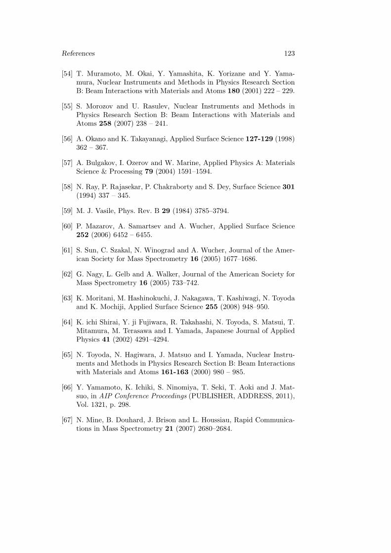
References 123
[54] T. Muramoto, M. Okai, Y. Yamashita, K. Yorizane and Y. Yama-mura, Nuclear Instruments and Methods in Physics Research SectionB: Beam Interactions with Materials and Atoms 180 (2001) 222 – 229.
[55] S. Morozov and U. Rasulev, Nuclear Instruments and Methods inPhysics Research Section B: Beam Interactions with Materials andAtoms 258 (2007) 238 – 241.
[56] A. Okano and K. Takayanagi, Applied Surface Science 127-129 (1998)362 – 367.
[57] A. Bulgakov, I. Ozerov and W. Marine, Applied Physics A: MaterialsScience & Processing 79 (2004) 1591–1594.
[58] N. Ray, P. Rajasekar, P. Chakraborty and S. Dey, Surface Science 301(1994) 337 – 345.
[59] M. J. Vasile, Phys. Rev. B 29 (1984) 3785–3794.
[60] P. Mazarov, A. Samartsev and A. Wucher, Applied Surface Science252 (2006) 6452 – 6455.
[61] S. Sun, C. Szakal, N. Winograd and A. Wucher, Journal of the Amer-ican Society for Mass Spectrometry 16 (2005) 1677–1686.
[62] G. Nagy, L. Gelb and A. Walker, Journal of the American Society forMass Spectrometry 16 (2005) 733–742.
[63] K. Moritani, M. Hashinokuchi, J. Nakagawa, T. Kashiwagi, N. Toyodaand K. Mochiji, Applied Surface Science 255 (2008) 948–950.
[64] K. ichi Shirai, Y. ji Fujiwara, R. Takahashi, N. Toyoda, S. Matsui, T.Mitamura, M. Terasawa and I. Yamada, Japanese Journal of AppliedPhysics 41 (2002) 4291–4294.
[65] N. Toyoda, N. Hagiwara, J. Matsuo and I. Yamada, Nuclear Instru-ments and Methods in Physics Research Section B: Beam Interactionswith Materials and Atoms 161-163 (2000) 980 – 985.
[66] Y. Yamamoto, K. Ichiki, S. Ninomiya, T. Seki, T. Aoki and J. Mat-suo, in AIP Conference Proceedings (PUBLISHER, ADDRESS, 2011),Vol. 1321, p. 298.
[67] N. Mine, B. Douhard, J. Brison and L. Houssiau, Rapid Communica-tions in Mass Spectrometry 21 (2007) 2680–2684.
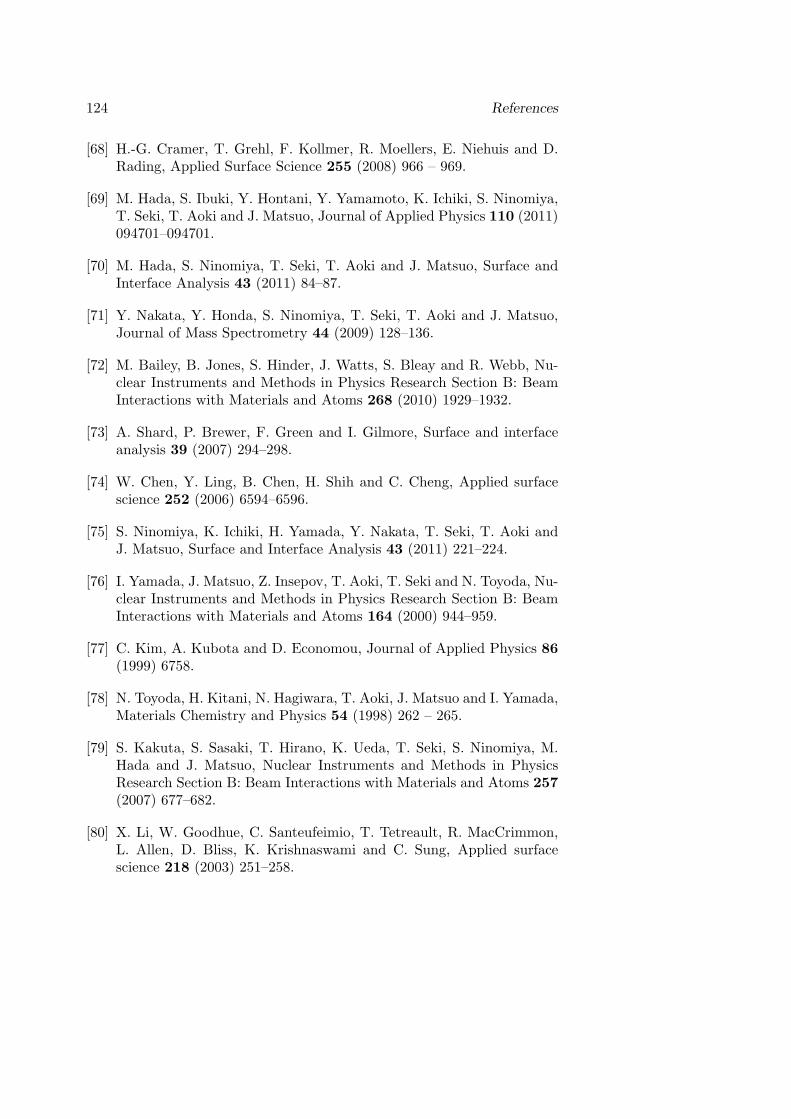
124 References
[68] H.-G. Cramer, T. Grehl, F. Kollmer, R. Moellers, E. Niehuis and D.Rading, Applied Surface Science 255 (2008) 966 – 969.
[69] M. Hada, S. Ibuki, Y. Hontani, Y. Yamamoto, K. Ichiki, S. Ninomiya,T. Seki, T. Aoki and J. Matsuo, Journal of Applied Physics 110 (2011)094701–094701.
[70] M. Hada, S. Ninomiya, T. Seki, T. Aoki and J. Matsuo, Surface andInterface Analysis 43 (2011) 84–87.
[71] Y. Nakata, Y. Honda, S. Ninomiya, T. Seki, T. Aoki and J. Matsuo,Journal of Mass Spectrometry 44 (2009) 128–136.
[72] M. Bailey, B. Jones, S. Hinder, J. Watts, S. Bleay and R. Webb, Nu-clear Instruments and Methods in Physics Research Section B: BeamInteractions with Materials and Atoms 268 (2010) 1929–1932.
[73] A. Shard, P. Brewer, F. Green and I. Gilmore, Surface and interfaceanalysis 39 (2007) 294–298.
[74] W. Chen, Y. Ling, B. Chen, H. Shih and C. Cheng, Applied surfacescience 252 (2006) 6594–6596.
[75] S. Ninomiya, K. Ichiki, H. Yamada, Y. Nakata, T. Seki, T. Aoki andJ. Matsuo, Surface and Interface Analysis 43 (2011) 221–224.
[76] I. Yamada, J. Matsuo, Z. Insepov, T. Aoki, T. Seki and N. Toyoda, Nu-clear Instruments and Methods in Physics Research Section B: BeamInteractions with Materials and Atoms 164 (2000) 944–959.
[77] C. Kim, A. Kubota and D. Economou, Journal of Applied Physics 86(1999) 6758.
[78] N. Toyoda, H. Kitani, N. Hagiwara, T. Aoki, J. Matsuo and I. Yamada,Materials Chemistry and Physics 54 (1998) 262 – 265.
[79] S. Kakuta, S. Sasaki, T. Hirano, K. Ueda, T. Seki, S. Ninomiya, M.Hada and J. Matsuo, Nuclear Instruments and Methods in PhysicsResearch Section B: Beam Interactions with Materials and Atoms 257(2007) 677–682.
[80] X. Li, W. Goodhue, C. Santeufeimio, T. Tetreault, R. MacCrimmon,L. Allen, D. Bliss, K. Krishnaswami and C. Sung, Applied surfacescience 218 (2003) 251–258.

References 125
[81] J. Song, D. Choi and W. Choi, Nuclear Instruments and Methods inPhysics Research Section B: Beam Interactions with Materials andAtoms 196 (2002) 275–278.
[82] Z. Postawa, B. Czerwinski, M. Szewczyk, E. Smiley, N. Winograd andB. Garrison, The Journal of Physical Chemistry B 108 (2004) 7831–7838.
[83] T. Aoki, T. Seki and J. Matsuo, Vacuum 84 (2010) 994 – 998.
[84] L. Allen, Z. Insepov, D. Fenner, C. Santeufemio, W. Brooks, K. Jonesand I. Yamada, Journal of applied physics 92 (2002) 3671.
[85] T. Aoki, J. Matsuo and I. Yamada, Nuclear Instruments and Methodsin Physics Research Section B: Beam Interactions with Materials andAtoms 180 (2001) 164–170.
[86] Z. Insepov, R. Manory, J. Matsuo and I. Yamada, Physical Review B61 (2000) 8744.
[87] T. Seki and J. Matsuo, Nuclear Instruments and Methods in PhysicsResearch Section B: Beam Interactions with Materials and Atoms 241(2005) 604 – 608.
[88] N. Toyoda, Y. Maeshima and I. Yamada, Nuclear Instruments andMethods in Physics Research Section B: Beam Interactions with Ma-terials and Atoms 257 (2007) 662 – 665.


List of Publications
Publications
1. S. Ninomiya, K. Ichiki, H. Yamada, Y. Nakata, T. Seki, T. Aoki, J.Matsuo “Analysis of organic semiconductor multilayers with Ar clus-ter secondary ion mass spectrometry” Surface and Interface AnalysisVol. 43[1-2],(2011) pp.95-98
2. S. Ninomiya, K. Ichiki, H. Yamada, Y. Nakata, T. Seki, T. Aoki, J.Matsuo “The effect of incident energy on molecular depth profilingof polymers with large Ar cluster ion beams” Surface and InterfaceAnalysis Vol. 43[1-2],(2011) pp.221-224
3. K. Ichiki, S. Ninomiya, Y. Nakata, H. Yamada, T. Seki, T. Aoki,J. Matsuo “Surface morphology of PMMA surfaces bombarded withsize-selected gas cluster ion beams” Surface and Interface AnalysisVol. 43[1-2] (2011) pp. 120-122
4. M. Hada, K. Ichikiand J. Matsuo “Characterization of vapor-depositedL-leucine nanofilm” Thin Solid Films 519, (2011) pp.1993-1997
5. S. Ninomiya, K. Ichiki, H. Yamada, Y. Nakata, T. Seki, T. Aoki, J.Matsuo “SIMS Depth Profiling of Organic Materials with Ar ClusterIon Beam”, Transactions of the MRS-J 35 [4] (2010) pp. 785-788
6. K. Ichiki, S. Ninomiya, T. Seki, T. Aoki, J. Matsuo “Sputtering Prop-erties of Si by Size-Selected Ar Gas Cluster Ion Beam” Transactionsof the MRS-J 35 [4] (2010) pp. 789-792
7. H. Yamada, K. Ichiki, Y. Nakata, S. Ninomiya, T. Seki, T. Aoki, J.Matsuo, “Processing Techniques of Biomaterials: Using Gas ClusterIon Beam for Imaging Mass Spectrometry” Transactions of the MRS-J 35 [4] (2010) pp. 793-796
8. M. Hada, Y. Hontani, S. Ibuki, K. Ichiki, S. Ninomiya, T. Seki, T.Aoki and J. Matsuo “Evaluation of Surface Damage of Organic Films
127

128 List of Publications
due to Irradiation with Energetic Ion Beams” AIP Conference Pro-ceedings Vol. 1321 (IIT2010), (2010) pp. 314-316
9. K. Ichiki, S. Ninomiya, T. Seki, T. Aoki, and J. Matsuo “EnergyEffects on the Sputtering Yield of Si Bombarded with Gas ClusterIon Beams” AIP Conference Proceedings Vol. 1321 (IIT2010) , (2010)pp. 294-297
10. Y. Yamamoto, K. Ichiki, S. Ninomiya, T. Seki, T. Aoki and J. Matsuo“Evaluation of surface damage on organic materials irradiated with Arcluster ion beam” AIP Conference Proceedings Vol. 1321 (IIT2010), (2010) pp. 298-301
11. J. Matsuo, S. Ninomiya, H. Yamada, K. Ichiki, Y. Wakamatsu, M.Hada, T. Seki and T. Aoki “SIMS with highly excited primary beamsfor molecular depth profiling and imaging for organic and biologicalmaterials” Surface and Interface Analysis Vol. 42 [10-11], (2010) pp.1612-1615
12. H. Yamada, K. Ichiki, Y. Nakata, S. Ninomiya, T. Seki, T. Aoki andJ. Matsuo “MeV-Energy Probe SIMS Imaging of Major Componentsin Animal Cells Etched Using Large Gas Cluster Ions” Nuclear Instru-ments and Methods in Physics Research B, 268, (2010) pp. 1736-1740
13. K. Ichiki, S. Ninomiya, T. Seki, T. Aoki and J. Matsuo “SputteringYield Measurements with Size-selected Gas Cluster Ion Beams” MRSSymposium Proceedings (2009 MRS Spring Meetings)
14. S. Ninomiya, K. Ichiki, H. Yamada, Y. Nakata, T. Seki, T. Aoki andJ. Matsuo “Molecular depth profiling of multilayer structures of or-ganic semiconductor materials by secondary ion massspectrometrywith large argon cluster ion beams” Rapid Communications in MassSpectrometry, 23, (2009) pp. 3264-3268
15. S. Ninomiya, K. Ichiki, T. Seki, T. Aoki, J. Matsuo, “The emissionprocess of secondary ions from solids bombarded with large gas clus-ter ions” Nuclear Instruments and Methods in Physics Research B,267,(2009) pp. 2601-2604,
16. H. Yamada, K. Ichiki, Y. Nakata, S. Ninomiya, T. Seki, T. Aoki and J.Matsuo, “A Processing Technique for Cell Surfaces Using Gas ClusterIons for Imaging Mass Spectrometry” Journal of the Mass Spectrom-etry Society of Japan vol. 57, No. 3 (2009) pp.117-121,

Publications 129
17. S. Ninomiya, K. Ichiki, H. Yamada, Y. Nakata, T. Seki, T. Aoki,J. Matsuo “Precise and fast secondary ion mass spectrometry depthprofiling of polymer materials with large Ar cluster ion beams” RapidCommunications in Mass Spectrometry, Vol.23, (2009) pp.1601-1606
18. S. Ninomiya, K. Ichiki, H. Yamada, Y. Nakata, T. Seki, T. Aoki andJ. Matsuo “Low Damage Etching of Polymer Materials for DepthProfile Analysis Using Large Ar Cluster Ion Beam” Journal of SurfaceAnalysis Vol.15, No.3, (2009) pp.275-278
19. J. Matsuo, S. Ninomiya, Y. Nakata, Y. Honda, K. Ichiki, T. Seki andT. Aoki “What size of cluster is most appropriate for SIMS?” AppliedSurface Science 255, (2008) pp.1235-1238
20. S. Ninomiya, K. Ichiki, Y. Nakata, Y. Honda, T. Seki, T. Aoki andJ. Matsuo “Secondary ion emission from Si bombarded with largeAr cluster ions under UHV conditions” Applied Surface Science 255,(2008) pp 880-882
21. K. Ichiki, S. Ninomiya, Y. Nakata, Y. Honda, T. Seki, T. Aoki andJ. Matsuo “High sputtering yields of organic compounds by large gascluster ions” Applied Surface Science 255, (2008) pp 1148-1150
22. S. Ninomiya, Y. Nakata, Y. Honda, K. Ichiki, T. Seki, T. Aoki andJ. Matsuo, “A Fragment-free ionization technique for organic massspectrometry with large Ar cluster ions” Applied Surface Science 255,(2008) pp 1588-1590
23. S. Ninomiya, J. Matsuo, K. Ichiki, H. Yamada, Y. Nakata, Y. Honda,T. Seki and T. Aoki “Low Damage Etching and SIMS Depth Profilingwith Large Ar Cluster Ions” Transactions of the MRS-J 33 [4] (2008)pp.1043-1046
24. S. Ninomiya, K. Ichiki, Y. Nakata, T. Seki, T. Aoki and J. Matsuo“The Effect of Incident Cluster Ion Size on Secondary Ion YieldsProduced from Si” Transactions of the MRS-J 32 [4] (2007) pp.895-898
25. J. Matsuo, S. Ninomiya, Y. Nakata, K. Ichiki, T. Aoki, T. Seki “Sizeeffect in cluster collision on solid surfaces” Nuclear Instruments andMethods in Physics Research B 257 (2007) 627-631
26. S. Ninomiya, K. Ichiki, Y. Nakata, T. Seki, T. Aoki, J. Matsuo “Theeffect of incident cluster ion energy and size on secondary ion yieldsemitted from Si” Nuclear Instruments and Methods in Physics Re-search B, 256 (2007)pp. 528-531

130 List of Publications
27. S. Ninomiya, Y. Nakata, K. Ichiki, T. Seki, T. Aoki, and J. Matsuo,“Measurements of secondary ions emitted from organic compoundsbombarded with large gas cluster ions”, Nuclear Instruments andMethods in Physics Research B, 256 (2007)pp. 493-496
28. K. Ichiki, S. Ninomiya, T. Seki, T. Aoki, and J. Matsuo, “Surface ox-idation of Si assisted by irradiation with large gas cluster ion beam inan oxygen atmosphere”, Nuclear Instruments and Methods in PhysicsResearch B, 256 (2007) pp. 350-353
International Conference
1. K. Ichiki, T. Seki, T. Aoki and J. Matsuo “The effects of cluster sizeand energy on sputtering with gas cluster ion beams” E-MRS 2011Spring Meeting (Nice, France, 2011/5/9, Poster)
2. K. Ichiki, S. Ninomiya, T. Seki, T. Aoki and J. Matsuo “The effects ofcluster size on sputtering and surface smoothing with gas cluster ionbeams” 20th MRS-J Symposium(International Session)(Yokohama,Japan, 2010/12/22, Poster)
3. K. Ichiki, S. Ninomiya, T. Seki, T. Aoki and J. Matsuo “The effectsof cluster size and energy on surface smoothing with gas cluster ionbeams” 17th International Conference on Ion Beam Modification ofMaterials (IBMM2010), (Montreal, Canada, 2010/8/23, Poster)
4. K. Ichiki, S. Ninomiya, T. Seki, T. Aoki and J. Matsuo “The effects ofincident cluster size and energy on Si sputtering yield” 10th Workshopon Cluster Ion Beam Technology (Kyoto, Japan, 2010/6/14, Oral)
5. K. Ichiki, S. Ninomiya, T. Seki, T. Aoki and J. Matsuo “Size andenergy dependence of the sputtering yield of Si bombarded with gascluster ion beams” 18th International Conference on Ion ImplantationTechnology (Kyoto University, Japan, 2010/6/7, Poster)
6. K. Ichiki, S. Ninomiya, Y. Nakata, H. Yamada, T. Seki, T. Aoki and J.Matsuo “Sputtering and morphology of solid surfaces bombarded withsize-selected gas cluster ion beams” 16th International Conference onSurface Modification of Materials by Ion Beams (SMMIB2009) (AISTTokyo Waterfront, Japan, 2009/9/16, Oral)
7. K. Ichiki, S. Ninomiya, T. Seki, T. Aoki and J. Matsuo “Size effectsof sputtering yields with large cluster ion beams” 17th International

Awards 131
Conference on Secondary Ion Mass Spectrometry (Toronto, Canada,2009/9/14, Poster)
8. K. Ichiki, S. Ninomiya, M. Hada, T. Seki, T. Aoki and J. Mat-suo “Sputtering yield measurement with size-selected gas cluster ionbeams” 2009 MRS spring meeting (San Francisco, CA, 2009/4/16,Poster)
9. K. Ichiki, S. Ninomiya, T. Seki, T. Aoki and J. Matsuo “Size-selectedHigh Density Large Gas Cluster Ion Beam Irradiation” The IUMRSInternational Conference in Asia (Nagoya Congress Center, Japan,2008/12/11, Poster)
10. K. Ichiki, S. Ninomiya, Y. Nakata, Y. Honda, T. Seki, T. Aoki and J.Matsuo, “High sputtering yields of organic compounds by large gascluster ions” The 16th International Conference on Secondary IonMass Spectrometry(Kanazawa, Japan, 2007/10/29-11/2)
11. K. Ichiki, S. Ninomiya, T. Seki, T. Aoki and J. Matsuo, “Nonlin-ear effects of secondary ion yields emitted from Si by Ar cluster ionbeam irradiation” The 16th International Conference on SecondaryIon Mass Spectrometry(Kanazawa, Japan, 2007/10/29-11/2)
12. K. Ichiki, S. Ninomiya, T. Seki, T. Aoki and J. Matsuo, “Surfaceoxidation of Si assisted by irradiation with large gas cluster ion beamin an oxygen atmosphere”, 22nd International Conference on AtomicCollisions in Solids, (Berlin, Germany, 2006/7/21-26).
Awards
1. Award for Encouragement of ResearchThe IUMRS International Conference in Asia 2008, Nagoya, Japan,November 2008.
2. Surface Science Western SIMS Research Award for PosterThe 17th International Conference on Secondary Ion Mass Spectrom-etry, Toronto, Canada, September 2009.
3. Award for Encouragement of Research20th Symposium of Material Research Society of Japan,Tokyo, Japan,December 2010.