tl494 pulse - width- modulation control circuits managemant/tl494.pdf · pad location tl494 chip...
TRANSCRIPT
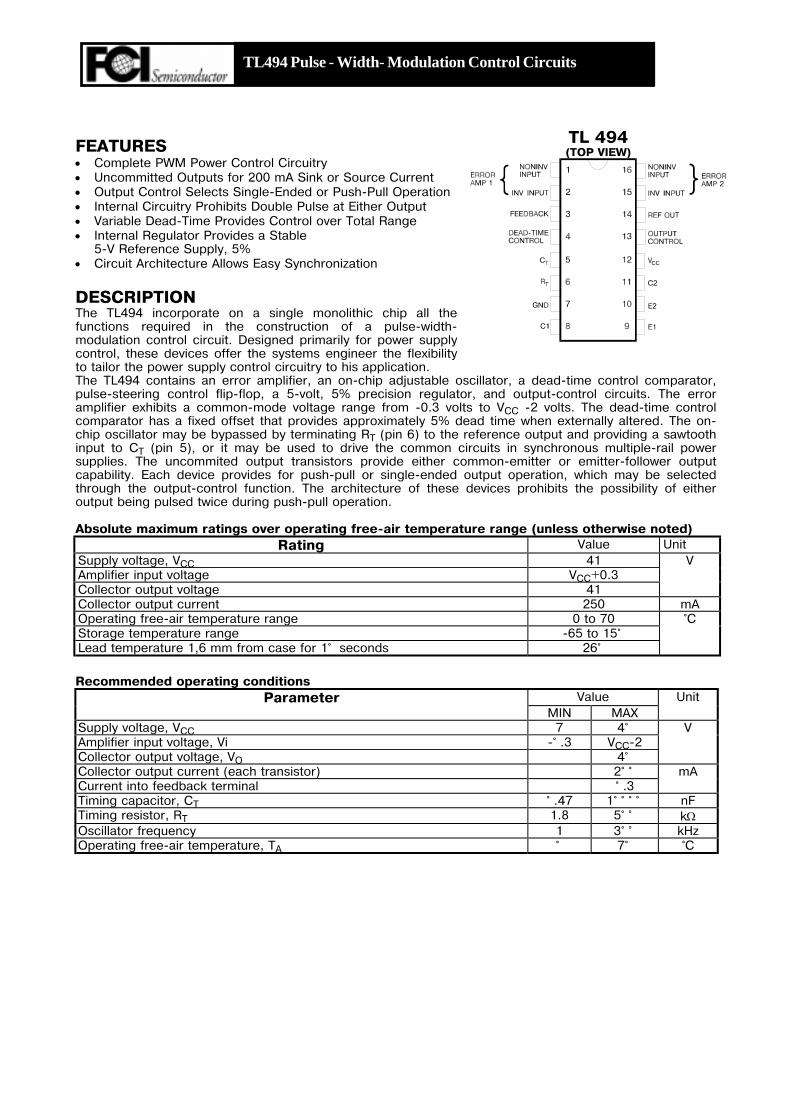
FEATURES • Complete PWM Power Control Circuitry • Uncommitted Outputs for 200 mA Sink or Source Current • Output Control Selects Single-Ended or Push-Pull Operation • Internal Circuitry Prohibits Double Pulse at Either Output • Variable Dead-Time Provides Control over Total Range • Internal Regulator Provides a Stable
5-V Reference Supply, 5% • Circuit Architecture Allows Easy Synchronization
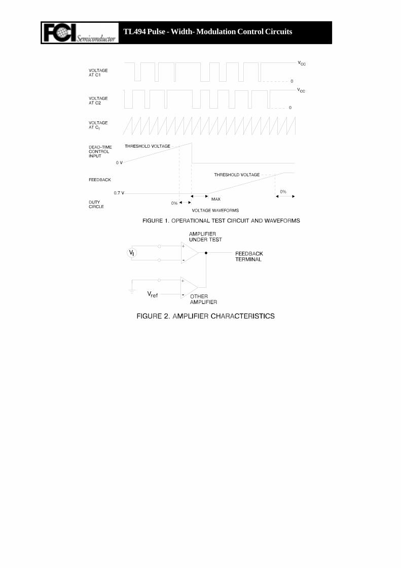
DESCRIPTION The TL494 incorporate on a single monolithic chip all the functions required in the construction of a pulse-width-modulation control circuit. Designed primarily for power supply control, these devices offer the systems engineer the flexibility to tailor the power supply control circuitry to his application. The TL494 contains an error amplifier, an on-chip adjustable oscillator, a dead-time control comparator, pulse-steering control flip-flop, a 5-volt, 5% precision regulator, and output-control circuits. The error amplifier exhibits a common-mode voltage range from -0.3 volts to VCC -2 volts. The dead-time control comparator has a fixed offset that provides approximately 5% dead time when externally altered. The on-chip oscillator may be bypassed by terminating RT (pin 6) to the reference output and providing a sawtooth input to CT (pin 5), or it may be used to drive the common circuits in synchronous multiple-rail power supplies. The uncommited output transistors provide either common-emitter or emitter-follower output capability. Each device provides for push-pull or single-ended output operation, which may be selected through the output-control function. The architecture of these devices prohibits the possibility of either output being pulsed twice during push-pull operation. Absolute maximum ratings over operating free-air temperature range (unless otherwise noted)
Rating Value Unit Supply voltage, VCC 41 V Amplifier input voltage VCC+0.3 Collector output voltage 41 Collector output current 250 mA Operating free-air temperature range 0 to 70 0C Storage temperature range -65 to 150 Lead temperature 1,6 mm from case for 10 seconds 260
Recommended operating conditions
Parameter Value Unit MIN MAX Supply voltage, VCC 7 40 V Amplifier input voltage, Vi -0 .3 VCC-2 Collector output voltage, VO 40 Collector output current (each transistor) 20 0 mA Current into feedback terminal 0 .3 Timing capacitor, CT 0 .47 10 0 0 0 nF Timing resistor, RT 1.8 50 0 kΩ Oscillator frequency 1 30 0 kHz Operating free-air temperature, TA 0 70 0C
TL 494 (TOP VIEW)
TL494 Pulse - Width- Modulation Control Circuits
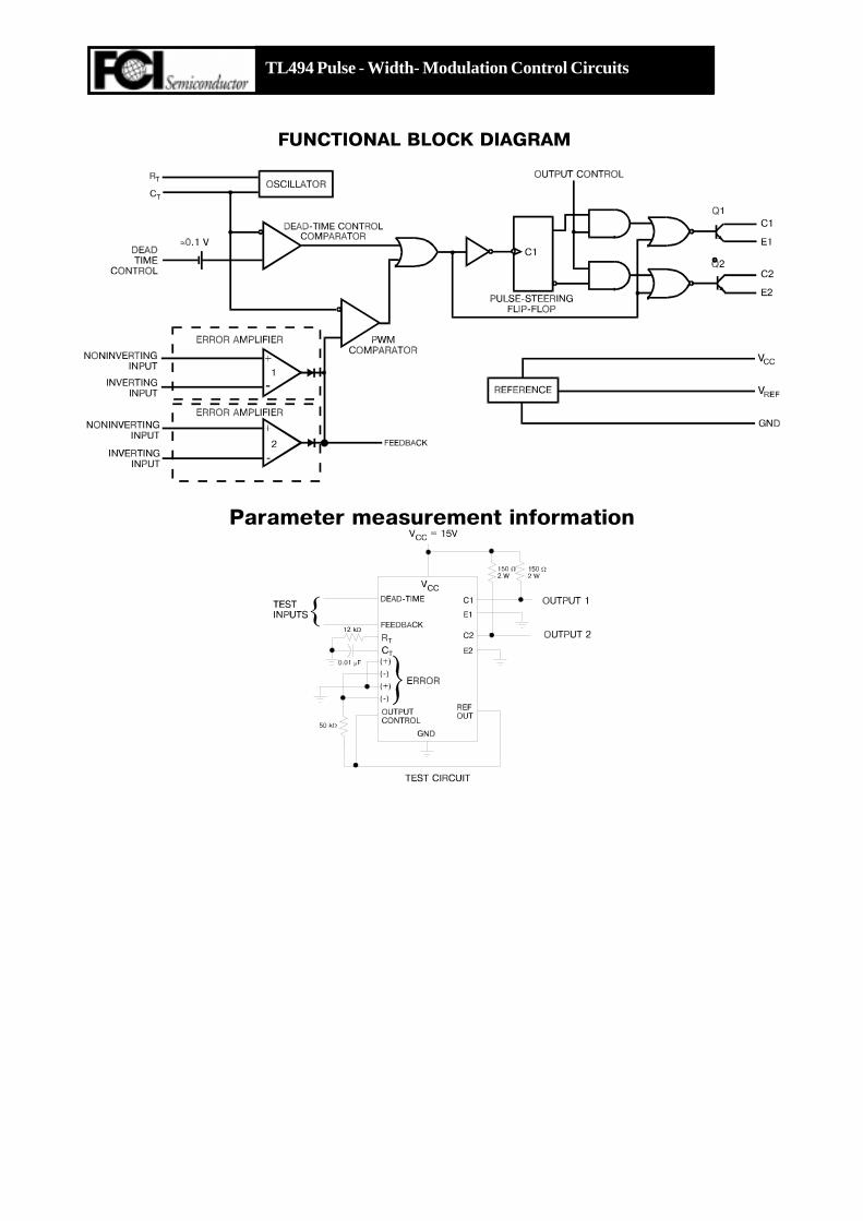
FUNCTIONAL BLOCK DIAGRAM
Parameter measurement information
TL494 Pulse - Width- Modulation Control Circuits
TL494 Pulse - Width- Modulation Control Circuits
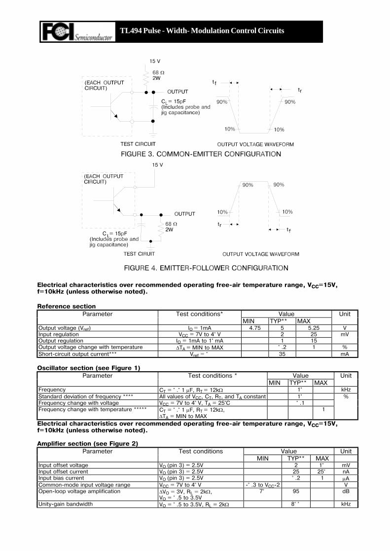
Electrical characteristics over recommended operating free-air temperature range, VCC=15V, f=10kHz (unless otherwise noted). Reference section
Parameter Test conditions* Value Unit MIN TYP** MAX Output voltage (Vref) lO = 1mA 4.75 5 5.25 V Input regulation VCC = 7V to 40 V 2 25 mV Output regulation IO = 1mA to 10 mA 1 15 Output voltage change with temperature ∆TA = MIN to MAX 0 .2 1 % Short-circuit output current*** Vref = 0 35 mA
Oscillator section (see Figure 1)
Parameter Test conditions * Value Unit MIN TYP** MAX Frequency CT = 0 .0 1 µF, RT = 12kΩ 10 kHz Standard deviation of frequency **** All values of VCC, CT, RT, and TA constant 10 % Frequency change with voltage VCC = 7V to 40 V, TA = 250C 0 .1 Frequency change with temperature ***** CT = 0 .0 1 µF, RT = 12kΩ,
∆TA = MIN to MAX 1
Electrical characteristics over recommended operating free-air temperature range, VCC=15V, f=10kHz (unless otherwise noted). Amplifier section (see Figure 2)
Parameter Test conditions Value Unit MIN TYP** MAX Input offset voltage VO (pin 3) = 2.5V 2 10 mV Input offset current VO (pin 3) = 2.5V 25 250 nA Input bias current VO (pin 3) = 2.5V 0 .2 1 µA Common-mode input voltage range VCC = 7V to 40 V -0 .3 to VCC-2 V Open-loop voltage amplification ∆VO = 3V, RL = 2kΩ,
VO = 0 .5 to 3.5V 70 95 dB
Unity-gain bandwidth VO = 0 .5 to 3.5V, RL = 2kΩ 80 0 kHz
TL494 Pulse - Width- Modulation Control Circuits

Common-mode rejection ratio ∆VO = 40 V, TA = 250C 65 80 dB Output sink current (pin 3) VID = -15mV to -5V,
V(pin3) = 0 .7 V 0 .3 0 .7 mA
Output source current (pin 3) VID = 15mV to 5V, V(pin3) = 3.5 V
-2 mA
* For conditions shown as MIN or MAX, use the appropriate value specified under recommended operating conditions. ** All typical values except for parameter changes with temperature are at TA = 25 0C *** Duration of the short-circuit should not exceed one second. **** Standard deviation Is a measure of the statistical distribution about the mean as derived from the formula
2/1
1
2
1)(
−
−=σ ∑
=
N
n
n
Nxx
***** Temperature coefficient of timing capacitor and timing resistor not taken Into account
Output section
Parameter Test conditions Value Unit MIN TYP* MAX Collector off-state current VCE=40 V, VCC=40 V 2 10 0 µA Emitter off-state current VCC=VC=40 V, VE=0 -10 0 Collector-emitter saturation Common-emitter VE=0 , IC=20 0 mA 1.1 1.3 V voltage Emitter-follower VC=15V, IE=-20 0 mA 1.5 2.5 Output control input current VI=Vref 3.5 mA
Dead-time control-section (see Figure 1)
Parameter Test conditions Value Unit MIN TYP* MAX Input bias current (pin 4) VI=0 to 5.25V -2 -10 µA Maximum duty cycle, each output VI (pin 4)=0 , CT=0 .1µF, RT=12kΩ 45 % Input threshold voltage (pin 4) Zero duty cycle 3 3.3 V Maximum duty cycle 0
PWM comparator section (see Figure 1)
Parameter Test conditions Value Unit MIN TYP* MAX
Input threshold voltage (pin 3) Zero duty cycle 4 4.5 V Input sink current (pin 3) V (pin 3) = 0 .7V 0 .3 0 .7 mA
Total device
Parameter Test conditions Value Unit MIN TYP* MAX
Standby supply current Pin 6 at Vref, all other inputs and VCC=15V 6 10 mA outputs open VCC=40 V 9 15 Average supply current VI (pin 4)=2V, See Figure 1 7.5
Switching characteristics, TA = 250C
Parameter Test conditions Value Unit MIN TYP* MAX
Output voltage rise time Common-emitter configuration, 10 0 20 0 ns Output voltage fall time See figure 3 25 10 0 Output voltage rise time Emitter-follower configuration. 10 0 20 0 Output voltage fall time See Figure 4 40 10 0 *AII typical values except for temperature coefficient are at TA=25 °C
TL494 Pulse - Width- Modulation Control Circuits

PAD LOCATION TL494
Chip size 2.0 5x2.3 mm
PAD LOCATION COORDINATES
Coordinates Pad N Pad Name
X (µm) Y (µm)
1 NONINV INPUT 130 5 120
2 INV INPUT 160 0 130
3 FEEDBACK 180 0 130
4 DEAD-TIME CONTROL 1810 370
5 CT 1795 975
6 RT 1770 1240
7 GND 1520 2135
8 C1 140 5 20 20
9 E1 10 55 20 15
10 E2 80 5 20 15
11 C2 460 20 20
12 VCC 140 1410
13 OUTPUT CONTROL 140 1260
14 REF OUT 160 375
15 INV INPUT 250 195
16 NONINV INPUT 40 5 195
TL494 Pulse - Width- Modulation Control Circuits