tle6251-3gdata sheet 4 rev. 1.1, 2011-06-06 tle6251-3g block diagram 2 block diagram figure 1 block...
TRANSCRIPT

Automot ive Power
Data Sheet Rev. 1.1, 2011-06-06
TLE6251-3GHigh Speed CAN-Transceiver with Wake and Failure Detection

Data Sheet 2 Rev. 1.1, 2011-06-06
TLE6251-3G
1 Overview . . . . . . . . . . . . . . . . . . . . . . . . . . . . . . . . . . . . . . . . . . . . . . . . . . . . . . . . . . . . . . . . . . . . . . . 3
2 Block Diagram . . . . . . . . . . . . . . . . . . . . . . . . . . . . . . . . . . . . . . . . . . . . . . . . . . . . . . . . . . . . . . . . . . . 4
3 Pin Configuration . . . . . . . . . . . . . . . . . . . . . . . . . . . . . . . . . . . . . . . . . . . . . . . . . . . . . . . . . . . . . . . . 53.1 Pin Assignment . . . . . . . . . . . . . . . . . . . . . . . . . . . . . . . . . . . . . . . . . . . . . . . . . . . . . . . . . . . . . . . . . . . 53.2 Pin Definitions and Functions . . . . . . . . . . . . . . . . . . . . . . . . . . . . . . . . . . . . . . . . . . . . . . . . . . . . . . . . 5
4 Functional Description . . . . . . . . . . . . . . . . . . . . . . . . . . . . . . . . . . . . . . . . . . . . . . . . . . . . . . . . . . . . 74.1 High Speed CAN Physical Layer . . . . . . . . . . . . . . . . . . . . . . . . . . . . . . . . . . . . . . . . . . . . . . . . . . . . . 7
5 Operation Modes . . . . . . . . . . . . . . . . . . . . . . . . . . . . . . . . . . . . . . . . . . . . . . . . . . . . . . . . . . . . . . . . 95.1 Normal Operation Mode . . . . . . . . . . . . . . . . . . . . . . . . . . . . . . . . . . . . . . . . . . . . . . . . . . . . . . . . . . . 105.2 Receive-Only Mode . . . . . . . . . . . . . . . . . . . . . . . . . . . . . . . . . . . . . . . . . . . . . . . . . . . . . . . . . . . . . . 105.3 Stand-By Mode . . . . . . . . . . . . . . . . . . . . . . . . . . . . . . . . . . . . . . . . . . . . . . . . . . . . . . . . . . . . . . . . . . 115.4 Go-To-Sleep Command . . . . . . . . . . . . . . . . . . . . . . . . . . . . . . . . . . . . . . . . . . . . . . . . . . . . . . . . . . . 125.5 Sleep Mode . . . . . . . . . . . . . . . . . . . . . . . . . . . . . . . . . . . . . . . . . . . . . . . . . . . . . . . . . . . . . . . . . . . . . 12
6 Wake-Up Functions . . . . . . . . . . . . . . . . . . . . . . . . . . . . . . . . . . . . . . . . . . . . . . . . . . . . . . . . . . . . . 146.1 Remote Wake-Up . . . . . . . . . . . . . . . . . . . . . . . . . . . . . . . . . . . . . . . . . . . . . . . . . . . . . . . . . . . . . . . . 146.2 Local Wake-Up . . . . . . . . . . . . . . . . . . . . . . . . . . . . . . . . . . . . . . . . . . . . . . . . . . . . . . . . . . . . . . . . . . 156.3 Mode Change via the EN and NSTB pin . . . . . . . . . . . . . . . . . . . . . . . . . . . . . . . . . . . . . . . . . . . . . . 16
7 Fail Safe Features . . . . . . . . . . . . . . . . . . . . . . . . . . . . . . . . . . . . . . . . . . . . . . . . . . . . . . . . . . . . . . . 177.1 CAN Bus Failure Detection . . . . . . . . . . . . . . . . . . . . . . . . . . . . . . . . . . . . . . . . . . . . . . . . . . . . . . . . . 177.2 Local Failures . . . . . . . . . . . . . . . . . . . . . . . . . . . . . . . . . . . . . . . . . . . . . . . . . . . . . . . . . . . . . . . . . . . 187.2.1 TxD Time-Out Feature . . . . . . . . . . . . . . . . . . . . . . . . . . . . . . . . . . . . . . . . . . . . . . . . . . . . . . . . . . . 187.2.2 TxD to RxD Short Circuit Feature . . . . . . . . . . . . . . . . . . . . . . . . . . . . . . . . . . . . . . . . . . . . . . . . . . 197.2.3 RxD Permanent Recessive Clamping . . . . . . . . . . . . . . . . . . . . . . . . . . . . . . . . . . . . . . . . . . . . . . . 197.2.4 Bus Dominant Clamping . . . . . . . . . . . . . . . . . . . . . . . . . . . . . . . . . . . . . . . . . . . . . . . . . . . . . . . . . 197.2.5 Over-Temperature Detection . . . . . . . . . . . . . . . . . . . . . . . . . . . . . . . . . . . . . . . . . . . . . . . . . . . . . . 207.3 Under-Voltage Detection . . . . . . . . . . . . . . . . . . . . . . . . . . . . . . . . . . . . . . . . . . . . . . . . . . . . . . . . . . 207.3.1 Under-Voltage Event on VCC and VIO . . . . . . . . . . . . . . . . . . . . . . . . . . . . . . . . . . . . . . . . . . . . . . . 207.3.2 Under-Voltage Event on VS . . . . . . . . . . . . . . . . . . . . . . . . . . . . . . . . . . . . . . . . . . . . . . . . . . . . . . . 227.4 Voltage Adaptation . . . . . . . . . . . . . . . . . . . . . . . . . . . . . . . . . . . . . . . . . . . . . . . . . . . . . . . . . . . . . . . 22
8 Diagnosis-Flags at NERR and RxD . . . . . . . . . . . . . . . . . . . . . . . . . . . . . . . . . . . . . . . . . . . . . . . . . 23
9 General Product Characteristics . . . . . . . . . . . . . . . . . . . . . . . . . . . . . . . . . . . . . . . . . . . . . . . . . . . 249.1 Absolute Maximum Ratings . . . . . . . . . . . . . . . . . . . . . . . . . . . . . . . . . . . . . . . . . . . . . . . . . . . . . . . . 249.2 Functional Range . . . . . . . . . . . . . . . . . . . . . . . . . . . . . . . . . . . . . . . . . . . . . . . . . . . . . . . . . . . . . . . . 259.3 Thermal Resistance . . . . . . . . . . . . . . . . . . . . . . . . . . . . . . . . . . . . . . . . . . . . . . . . . . . . . . . . . . . . . . 25
10 Electrical Characteristics . . . . . . . . . . . . . . . . . . . . . . . . . . . . . . . . . . . . . . . . . . . . . . . . . . . . . . . . . 2610.1 Functional Device Characteristics . . . . . . . . . . . . . . . . . . . . . . . . . . . . . . . . . . . . . . . . . . . . . . . . . . . 2610.2 Diagrams . . . . . . . . . . . . . . . . . . . . . . . . . . . . . . . . . . . . . . . . . . . . . . . . . . . . . . . . . . . . . . . . . . . . . . 30
11 Application Information . . . . . . . . . . . . . . . . . . . . . . . . . . . . . . . . . . . . . . . . . . . . . . . . . . . . . . . . . . 3111.1 Application Example . . . . . . . . . . . . . . . . . . . . . . . . . . . . . . . . . . . . . . . . . . . . . . . . . . . . . . . . . . . . . . 3111.2 ESD Robustness according to IEC61000-4-2 . . . . . . . . . . . . . . . . . . . . . . . . . . . . . . . . . . . . . . . . . . 3211.3 Voltage Drop over the INH Output . . . . . . . . . . . . . . . . . . . . . . . . . . . . . . . . . . . . . . . . . . . . . . . . . . . 3211.4 Mode Change to Sleep mode . . . . . . . . . . . . . . . . . . . . . . . . . . . . . . . . . . . . . . . . . . . . . . . . . . . . . . . 3311.5 Further Application Information . . . . . . . . . . . . . . . . . . . . . . . . . . . . . . . . . . . . . . . . . . . . . . . . . . . . . . 33
12 Package Outlines . . . . . . . . . . . . . . . . . . . . . . . . . . . . . . . . . . . . . . . . . . . . . . . . . . . . . . . . . . . . . . . 34
13 Revision History . . . . . . . . . . . . . . . . . . . . . . . . . . . . . . . . . . . . . . . . . . . . . . . . . . . . . . . . . . . . . . . . 35
Table of Contents

PG-DSO-14
Type Package MarkingTLE6251-3G PG-DSO-14 TLE6251-3G
Data Sheet 3 Rev. 1.1, 2011-06-06
High Speed CAN-Transceiver with Wake and Failure Detection
TLE6251-3G
1 Overview
Features• HS CAN Transceiver with data transmission rates up to 1 MBaud• Compliant to ISO 11898-5• Very low power consumption in Sleep mode• Bus Wake-Up and local Wake-Up• Inhibit output to control external circuitry • Separate VIO input to adapt different micro controller supply voltages• Separate output for failure diagnosis• Optimized for low electromagnetic emission (EME)• Optimized for a high immunity against electromagnetic interference (EMI)• Very high ESD robustness, ± 9 kV according to IEC 61000-4-2• Protected against automotive transients• Receive-Only mode for node failure analysis• TxD time-out function and RxD recessive clamping with failure indication• TxD to RxD short circuit recognition with failure indication• CANH and CANL short circuit recognition with failure indication• Bus dominant clamping diagnosis• Under-voltage detection at VCC, VIO and VS• Power-Up and Wake-Up source recognition• Short circuit proof and Over-Temperature protection • Green Product (RoHS compliant)• AEC Qualified
DescriptionAs a successor of the TLE6251G, the TLE6251-3G is designed to provide an excellent passive behavior in Power Down.This feature makes the TLE6251-3G extremely suitable for mixed power supply HS-CAN networks. The TLE6251-3Gprovides different operation modes with a very low quiescent current in Sleep mode. Based on the high symmetry of theCANH and CANL signals, the TLE6251-3G provides a very low level of electromagnetic emission (EME) within a broadfrequency range. The TLE6251-3G is integrated in a RoHS compliant PG-DSO-14 package and fulfills or exceeds therequirements of the ISO11898-5. The TLE6251G and the TLE6251-3G are fully pin compatible and function compatible.Based on the Infineon Smart Power Technology SPT®, the TLE6251-3G provides industry leading ESDrobustness together with a very high electromagnetic immunity (EMI). The Infineon Smart Power TechnologySPT® allows bipolar and CMOS control circuitry in accordance with DMOS power devices to exist on the samemonolithic circuit. The TLE6251-3G and the Infineon SPT® technology are AEC qualified and tailored to withstandthe harsh conditions of the automotive environment.

Data Sheet 4 Rev. 1.1, 2011-06-06
TLE6251-3G
Block Diagram
2 Block Diagram
Figure 1 Block Diagram
RxD
Driver
Temp.-Protection
TxD1
NSTB
EN
NERR8
VIO
7INH
Wake-UpComparator
13CANH
12
WK
3VCC
10
VS
11N.C.
2
GND
Normal Receiver
9
Mode ControlLogic
+timeout
Diagnosis & FailureLogic
Wake-Up Detection
RxD Output Control
Output Stage
CANL
Low Power Receiver
VCC/2
VS
VIO
VIO
4
5
14
6

TLE6251-3G
Pin Configuration
3 Pin Configuration
3.1 Pin Assignment
Figure 2 Pin Configuration
3.2 Pin Definitions and Functions9
Table 1 Pin Definitions and FunctionsPin Symbol Function1 TxD Transmit Data Input;
integrated pull-up resistor to VIO, “Low” for “Dominant” state.2 GND Ground3 VCC Transceiver Supply Voltage;
100 nF decoupling capacitor to GND recommend.4 RxD Receive Data Output;
“Low” in “Dominant” state. Output voltage level dependent on the VIO supply
5 VIO Logic Supply Voltage; Digital Supply Voltage for the logic pins TxD, RxD, EN, NERR and NSTB;Usually connected to the supply voltage of the external microcontroller;100 nF decoupling capacitor to GND recommend.
6 EN Mode Control Input; Integrated pull-down resistor;“High” for Normal Operation mode.
TxD 1
2
3
4
5
6
7 8
GND
VCC
RxD
NSTB
CANH
CANL
N.C.
VIO
EN
INH
VS
WK
NERR
9
10
11
12
13
14
Data Sheet 5 Rev. 1.1, 2011-06-06

TLE6251-3G
Pin Configuration
7 INH Inhibit Output; Open drain output to control external circuitry;High impedance in Sleep mode
8 NERR Error Flag Output; Failure and Wake-Up indication output, active “Low”Output voltage level depends on the VIO supply
9 WK Wake-Up Input; Local Wake-Up input;Wake-Up input sensitive to a level change in both directions, “High” to “Low” and vice versa.
10 VS Battery Voltage Supply; 100 nF decoupling capacitor to GND recommend.
11 N.C. Not Connected;12 CANL CAN Bus Low Level I/O;
“Low” in “Dominant” state13 CANH CAN Bus High Level I/O;
“High” in “Dominant” state14 NSTB Stand-By Control input;
Integrated pull-down resistor;“High” for Normal Operation mode.
Table 1 Pin Definitions and FunctionsPin Symbol Function
Data Sheet 6 Rev. 1.1, 2011-06-06
TLE6251-3G
Functional Description
4 Functional DescriptionCAN is a serial bus system that connects microcontrollers, sensor and actuators for real-time control applications.The usage of the Control Area Network (abbreviated CAN) within road vehicles is described by the internationalstandard ISO 11898. According to the 7 layer OSI reference model the physical layer of a CAN bus systemspecifies the data transmission from one CAN node to all other available CAN nodes inside the network. Thephysical layer specification of a CAN bus system includes all electrical and mechanical specifications of a CANnetwork. The CAN transceiver is part of the physical layer specification. Several different physical layer standardsof CAN networks have been developed over the last years. The TLE6251-3G is a High Speed CAN transceiverwith dedicated Wake-Up functions. High Speed CAN Transceivers with Wake-Up functions are defined by theinternational standard ISO 11898-5.
4.1 High Speed CAN Physical Layer
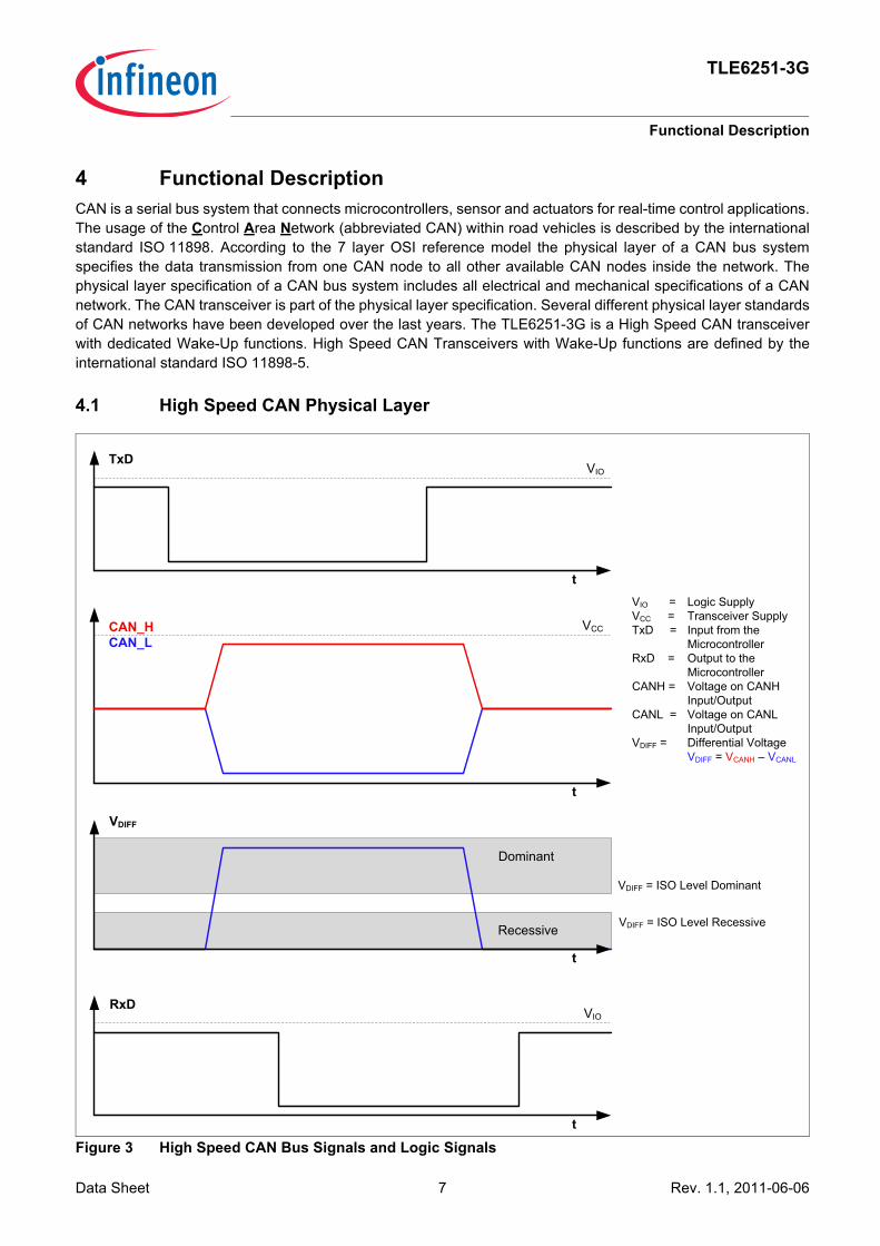
Figure 3 High Speed CAN Bus Signals and Logic Signals
VCCCAN_HCAN_L
TxD
VIO = Logic SupplyVCC = Transceiver SupplyTxD = Input from the
MicrocontrollerRxD = Output to the MicrocontrollerCANH = Voltage on CANH
Input/OutputCANL = Voltage on CANL
Input/OutputVDIFF = Differential Voltage
VDIFF = VCANH – VCANL
RxD
VDIFF
Dominant
Recessive
VIO
VIO
t
t
t
t
VDIFF = ISO Level Dominant
VDIFF = ISO Level Recessive
Data Sheet 7 Rev. 1.1, 2011-06-06
TLE6251-3G
Functional Description
The TLE6251-3G is a High Speed CAN transceiver, operating as an interface between the CAN controller and thephysical bus medium. A High Speed CAN network (abbreviated HS CAN) is a two wire differential network whichallows data transmission rates up to 1 MBaud. Characteristic for a HS CAN network are the two CAN bus states“Dominant” and “Recessive” (see Figure 3). A HS CAN network is a Carrier Sense Multiple Access network with Collision Detection. This means, everyparticipant of the CAN network is allowed to place its message on the same bus media simultaneously. This cancause data collisions on the bus, which might corrupt the information content of the data stream. In order avoidthe loss of any information and to prioritize the messages, it is essential that the “Dominant” bus signal overrulesthe “Recessive” bus signal. The input TxD and the output RxD are connected to the microcontroller of the ECU. As shown in Figure 1, theHS CAN transceiver TLE6251-3G has a receive unit and a output stage, allowing the transceiver to send data tothe bus medium and monitor the data from the bus medium at the same time. The HS CAN TLE6251-3G convertsthe serial data stream available on the transmit data input TxD into a differential output signal on CAN bus. Thedifferential output signal is provided by the pins CANH and CANL. The receiver stage of the TLE6251-3G monitorsthe data on the CAN bus and converts them to a serial data stream on the RxD pin. A logical “Low” signal on theTxD pin creates a “Dominant” signal on the CAN bus, followed by a logical “Low” signal on the RxD pin (seeFigure 3). The feature, broadcasting data to the CAN bus and listening to the data traffic on the CAN bussimultaneous is essential to support the bit to bit arbitration on CAN networks. The voltage levels for a HS CAN on the bus medium are defined by the ISO 11898-2/-5 standards. If a data bit is“Dominant” or “Recessive”, this depends on the voltage difference between CANH and CANL: VDIFF = VCANH - VCANL To transmit a “Dominant” signal to the CAN bus the differential signal VDIFF is larger or equal to 1.5 V. To receivea “Recessive” signal from the CAN bus the differential signal VDIFF is smaller or equal to 0.5 V. The voltage level on the digital input TxD and the digital output RxD is determined by the power supply level at thepin VIO. Depending on voltage level at the VIO pin, the signal levels on the logic pins (EN, NERR, NSTB, TxD andRxD) are compatible to microcontrollers with 5 V or 3.3 V I/O supply. Usually the VIO power supply of thetransceiver is connected to same power supply as I/O power supply of the microcontroller.Partially supplied CAN networks are networks where the participants have a different power supply status. Somenodes are powered up, other nodes are not powered, or some other nodes are in a Low-Power mode, like Sleepmode for example. Regardless on the supply status of the HS CAN node, each participant which is connected tothe common bus, shall not disturb the communication on the bus media. The TLE6251-3G is designed to supportpartially supplied networks. In Power Down condition, the resistors of the Normal Receiver are switched off andthe bus input on the pins CANH and CANL is high resistive.
Data Sheet 8 Rev. 1.1, 2011-06-06

TLE6251-3G
Operation Modes
5 Operation ModesFive different operation modes are available on TLE6251-3G. Each mode with specific characteristics in terms ofquiescent current, data transmission or failure diagnostic. For the mode selection the digital input pins EN andNSTB are used. Both digital input pins are event triggered. Figure 4 illustrates the different mode changesdepending on the status of the EN and NSTB pins. A mode change via the mode selections pins EN and NSTB isonly possible if the power supplies VCC, VIO and VS are activated.
Figure 4 Operation Modes
Under-voltage on VS
VS < VS,Poff
EN NSTB INH
Normal Operation mode
On11
EN NSTB INH
Stand-By mode
On00EN NSTB INH
Receive Only mode
On10
EN NSTB INH
Sleep mode
Off00
Go-To-Sleepcommand
EN NSTB INH01 On
Power Down
Under-voltage on VCC
Start – Up Supply VSSupply VCC within t < tUV(VCC)Supply VIO within t < tUV(VIO)
Under-voltage on VIO
EN -> 1 NSTB -> 1
EN -> 0 NSTB -> 0
EN = 1 NSTB -> 0
EN = 1 NSTB ->1
EN = 0 NSTB -> 0
EN = 0 NSTB -> 1
EN -> 0 NSTB = 1
EN -> 1 NSTB = 1
EN -> 1 NSTB -> 0
EN -> 0 NSTB -> 1
EN -> 1 NSTB = 0
EN -> 0 t < thSLPNSTB = 0
EN -> 0 t > thSLPNSTB = 0
thSLPTiming important for mode selection
EN = 0 NSTB -> 1VCC & VIO ON
EN -> 1 NSTB -> 1VCC & VIO ON
Wake-Up Event Bus-Wake:t > tBUSdomLocal-Wake:t > tWake
VIO < VIO,UV t > tUV(VIO)
VCC < VCC,UV t > tUV(VCC)
VS > VS,Pon
Data Sheet 9 Rev. 1.1, 2011-06-06

TLE6251-3G
Operation Modes
In Sleep mode the power supply VCC and the logic power supply VIO are usually turned off. A Wake-Up event, viathe CAN bus or the local Wake-Up pin, shifts the device from Sleep mode into Stand-By mode. The following operations mode are available on the TLE6251-3G:• Normal Operation mode• Receive-Only mode• Stand-By mode• Sleep mode• Go-To-Sleep CommandDepending on the operation mode, the output driver stage, the receiver stage and the bus biasing are active orinactive. Table 2 shows the different operation modes depending on the logic signal on the pins EN and NSTBwith the related status of the INH pin and the bus biasing.
5.1 Normal Operation ModeIn Normal Operation mode the HS CAN transceiver TLE6251-3G sends the serial data stream on the TxD pin tothe CAN bus while at the same time the data available on the CAN bus is monitored on the RxD output pin. InNormal Operation mode all functions of the TLE6251-3G are active:• The output stage is active and drives data from the TxD to the CAN bus.• The normal receiver unit is active and provides the data from the CAN bus to the RxD pin.• The low power receiver and the bus Wake-Up function is inactive.• The local Wake-Up pin is disabled.• The INH pin is connected to VS.• The RxD pin is “Low” for a “Dominant” bus signal and “High” for a “Recessive” bus signal”• The bus basing is set to VCC/2.• The failure detection is active and failures are indicated at the NERR pin. (see Chapter 8).• The under-voltage detection on the all 3 power supplies VCC, VIO and VS is active. The HS CAN transceiver TLE6251-3G enters Normal Operation mode by setting the mode selection pins EN andNSTB to logical “High” (see Table 2 or Figure 4).
5.2 Receive-Only ModeThe Receive-Only mode can be used to test the connection of the bus medium. The TLE6251-3G can still receivedata from the bus, but the output stage is disabled and therefore no data can be sent to the CAN bus. All otherfunctions are active:• The output stage is disabled and data which is available on the TxD pin will be blocked and not communicated
to the CAN bus.• The normal receiver unit is active and provides the data which is available on the CAN bus to the RxD pin.• The INH pin is connected to VS.• The RxD pin is “Low” for a “Dominant” bus signal and “High” for a “Recessive” bus signal.• The bus biasing is set to VCC/2.
Table 2 Overview Operation ModesOperation mode EN NSTB INH Bus BiasNormal Operation 1 1 VS VCC/2Receive-Only 0 1 VS VCC/2Stand-By 0 0 VS GNDGo-To-Sleep 1 0 VS GNDSleep 0 0 Floating GNDPower Down 0 0 Floating Floating
Data Sheet 10 Rev. 1.1, 2011-06-06

TLE6251-3G
Operation Modes
• The low power receiver and the bus Wake-Up function is inactive.• The local Wake-Up pin WK is disabled.• The failure diagnostic is active and local failures are indicated at the NERR pin (see Chapter 8).• The under-voltage detection on the all 3 power supplies VCC, VIO and VS is active. The HS CAN transceiver TLE6251-3G enters Receive-Only mode by setting the EN pin to logical “Low” and theNSTB to logical “High” (see Table 2 or Figure 4).
5.3 Stand-By ModeAfter the power-up sequence the TLE6251-3G enters automatically into Stand-By mode. Stand-By mode is an idlemode of the TLE6251-3G with optimized power consumption. In Stand-By mode the TLE6251-3G can not sendor receive any data. The output driver stage and the normal receiver unit are disabled. Both CAN bus pins, CANHand CANL are connected to GND. The following functions are available in Stand-By mode:• The output stage is disabled.• The normal receiver unit is disabled.• The low power receiver is active and monitors the CAN bus. In case of a message on the CAN bus the
TLE6251-3G sets an internal Wake-Up flag. If the power supplies VCC and VIO are active, the Wake-Up event is indicated by the RxD pin and the NERR pin (see Chapter 8).
• The local Wake-Up pin is active and a local Wake-Up event is indicated by the RxD and NERR pin, if the power supplies VCC and VIO are active (see Chapter 8).
• The INH output is active and set to VS.• Through the internal resistors RI (see Figure 1), the pins CANH and CANL are connected to GND.• If the power supplies VCC and VIO are active, the RxD pin indicates the Wake-Up events.• The TxD pin is disabled• The failure diagnostic is disabled.• The under-voltage detection on the all 3 power supplies VCC, VIO and VS is active. • The TLE6251-3G detects a Power-Up event and indicates it at the NERR pin (see Chapter 8).There are several ways to enter the Stand-By mode (see Figure 4):• After the start-up sequence the device enters per default Stand-By mode. Mode changes are only possible if
VCC and VIO are present.• The device is in Sleep mode and a Wake-Up event occurs.• The device is in the Go-To-Sleep command and the EN pin goes low before the time t < thSLP has expired.• The device is in Normal Operation mode or Receive-Only mode and the EN pin and NSTB pin are set to logical
“Low”.• An under-voltage event occurs on the power supply VS. In case of an under-voltage event, the TLE6251-3G
device always changes to Stand-By mode regardless in which mode the device currently operates.
Data Sheet 11 Rev. 1.1, 2011-06-06
TLE6251-3G
Operation Modes
5.4 Go-To-Sleep CommandThe Go-To-Sleep command is a transition mode allowing external circuitry like a microcontroller to prepare theECU for the Sleep mode. The TLE6251-3G stays in the Go-To-Sleep command for the maximum time t = thSLP,after exceeding the time thSLP the device changes into Sleep mode. A mode change into Sleep mode is onlypossible via the Go-To-Sleep command. During the Go-To-Sleep command the following functions on theTLE6251-3G are available:• The output driver stage is disabled. • The normal receiver unit is disabled.• The low power receiver is active and monitors the CAN bus. In case of a message on the CAN bus the
TLE6251-3G sets an internal Wake-Up flag. • The local Wake-Up pin is active and can detect a local Wake-Up event. • The INH output is active and set to VS.• Through the internal resistors RI (see Figure 1), the pins CANH and CANL are connected to GND.• The TxD pin is disabled.• The failure diagnostic is disabled.• The under-voltage detection on all 3 power supplies VCC, VIO and VS is active. Setting the NSTB pin to logical “Low”, while the EN signal remains at logical “High”, activates the Go-To-Sleepcommand. The Go-To-Sleep command can be entered from Normal Operation mode, Receive-Only mode andfrom Stand-By mode.
5.5 Sleep ModeThe Sleep mode is a power save mode. In Sleep mode the current consumption of the TLE6251-3G is reduced toa minimum while the device is still able to Wake-Up by a message on the CAN bus or a local Wake-Up event onthe pin WK. Most of the functions of the TLE6251-3G are disabled: • The output driver stage is disabled. • The normal receiver unit is disabled.• The low power receiver is active and monitors the CAN bus. In case of a message on the CAN bus the
TLE6251-3G changes from Sleep mode to Stand-By mode and sets an internal Wake-Up flag. • The local Wake-Up pin is active and in case of a signal change on the WK pin the operation mode changes to
Stand-By mode.• The INH output is floating.• Through the internal resistors RI (see Figure 1), the pins CANH and CANL are connected to GND.• If the power supplies VCC and VIO are present, the RxD pin indicates the Wake-Up event.• The TxD pin is disabled• The under-voltage detection on the power supply VS is active and sends the device into Stand-By mode in case
of an under-voltage event. There are only two ways to enter Sleep mode:• The device can activate the Sleep mode via the mode control pins EN and NSTB. • An under-voltage event on the power supplies VCC and VIO changes the operation mode to Sleep mode.
Data Sheet 12 Rev. 1.1, 2011-06-06

TLE6251-3G
Operation Modes
In order to enter the Stand-By mode or the Sleep mode, the EN signal needs to be set to logical “Low” a definedtime after the NSTB pin was set to logical “Low”. Important for the mode selection is the timing between the fallingedge of the NSTB signal and the EN signal. If the logical signal on the EN pin goes low before the transition timet < thSLP has been reached, the TLE6251-3G enters into Stand-By mode and the INH pin remains connected to theVS supply. In the case the logical signal on the EN pin goes low after the transition time t > thSLP, the TLE6251-3Genters into Sleep mode simultaneous with the expiration of the time window thSLP and the INH becomesdisconnected from the VS supply and is floating. (see Figure 5).
Figure 5 Entering Sleep Mode or Stand-By Mode
The signal on the CAN bus has no impact to mode changes. The operation mode can be changed regardless ifthe CAN bus is “Dominant” or “Recessive”.
EN
NSTB
INH
t < thSLP
Go-To Sleep command Stand-By modeNormal Operation
mode
thSLP
EN
NSTB
INH
t > thSLP
Go-To Sleep command Sleep modeNormal Operation
mode
thSLP
t
t
t
t
t
t
Data Sheet 13 Rev. 1.1, 2011-06-06

TLE6251-3G
Wake-Up Functions
6 Wake-Up FunctionsThere are several possibilities for a mode change from Sleep mode to another operation mode.• Remote Wake-Up via a message on the CAN bus.• Local Wake-Up via a signal change on the pin WK.• A status change of the logical signals applied to the mode control pins EN and NSTB.• An under-voltage detection on the VS power supply.In typical applications the power supplies VCC and VIO are turned off in Sleep mode, meaning a mode change canonly be caused by an external event, also called Wake-Up. In case the VCC and VIO power supply are available, amode change can be simple caused by changing the status on the mode control pins EN and NSTB.
6.1 Remote Wake-UpA remote Wake-Up or also called bus Wake-Up occurs via a CAN bus message and changes the operation modefrom Sleep mode to Stand-By mode. A signal change from “Recessive” to “Dominant”, followed by a “Dominant”signal for the time t > tWake initiates a bus Wake-Up (see Figure 6).
Figure 6 Remote Wake-Up
In case the time of the “Dominant” signal on the CAN bus is shorter than the filtering time tWake, no bus Wake-Upoccurs. The filter time is implemented to protect the HS CAN transceiver TLE6251-3G against unintended busWake-Up’s, triggered by spikes on the CAN bus. The signal change on the CAN bus from “Recessive” to“Dominant” is mandatory, a permanent “Dominant” signal would not activate any bus Wake-Up. In Stand-By mode the RxD output pin and the NERR output pin display the CAN bus Wake-Up event by a logical“Low” signal (Details see Chapter 8). Once the HS CAN Transceiver TLE6251-3G has recognized the Wake-Upevent and has changed to Stand-By mode, the INH output pin becomes active and provides the voltage VS to theexternal circuitry.
CANHCANL
INH
t > tWake
Go-To Sleep
commandStand-By mode
Normal Operation
mode
t
t
Sleep mode
„Recessive“ to „Dominant“ change
t < tWake
No Wake-Up
Wake-Up
Data Sheet 14 Rev. 1.1, 2011-06-06

TLE6251-3G
Wake-Up Functions
6.2 Local Wake-UpThe TLE6251-3G can be activated from Sleep mode by a signal change on the WK pin, also called local Wake-Up. Designed to withstand voltages up to 40V the WK pin can be directly connected to VS. The internal logic onthe WK pin works bi-sensitive, meaning the Wake-Up logic on the pin WK triggers on a both signal changes, from“High” to “Low” and from “Low” to “High” (see Figure 7).
Figure 7 Local Wake - Up
A filter time tWK(local) is implemented to protect the TLE6251-3G against unintended Wake-Up’s, caused by spikeson the pin WK. The threshold values VWK,H and VWK,L depend on the level of the VS power supply. In Stand-By mode the RxD output pin and the NERR output pin display the CAN bus Wake-Up event by a logical“Low” signal (Details see Chapter 8). Once the HS CAN Transceiver TLE6251-3G has recognized the Wake-Upevent and has changed to Stand-By mode, the INH output pin becomes active and provides the voltage VS to theexternal circuitry.
VWK
INH
t > tWk(local)
Stand-By mode
t
t
Sleep mode
Wake-Upt < tWk(local)
No Wake-Up
VWK
INH
t > tWk(local)
Stand-By Mode
t
t
Sleep Mode
Wake-Up
t < tWk(local)
No Wake-Up
Stand-By modeSleep mode
VWK,H
VWK,L
Data Sheet 15 Rev. 1.1, 2011-06-06
TLE6251-3G
Wake-Up Functions
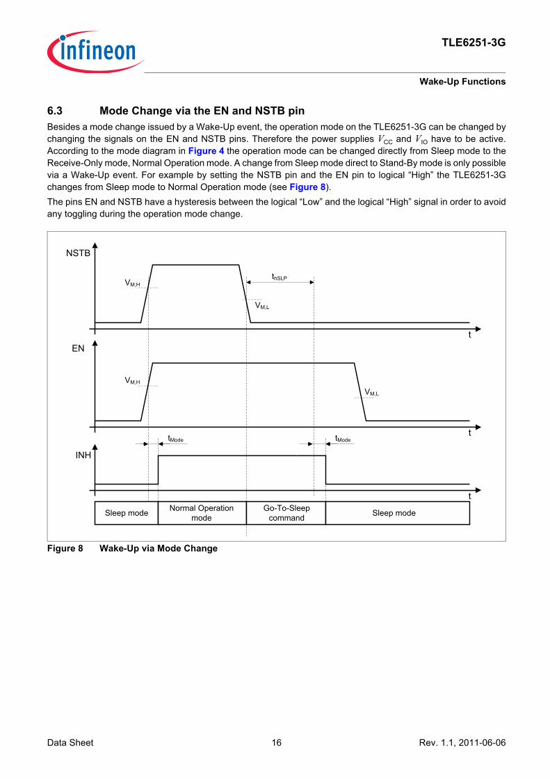
6.3 Mode Change via the EN and NSTB pinBesides a mode change issued by a Wake-Up event, the operation mode on the TLE6251-3G can be changed bychanging the signals on the EN and NSTB pins. Therefore the power supplies VCC and VIO have to be active.According to the mode diagram in Figure 4 the operation mode can be changed directly from Sleep mode to theReceive-Only mode, Normal Operation mode. A change from Sleep mode direct to Stand-By mode is only possiblevia a Wake-Up event. For example by setting the NSTB pin and the EN pin to logical “High” the TLE6251-3Gchanges from Sleep mode to Normal Operation mode (see Figure 8). The pins EN and NSTB have a hysteresis between the logical “Low” and the logical “High” signal in order to avoidany toggling during the operation mode change.
Figure 8 Wake-Up via Mode Change
EN
INH
t
t
VM,H
VM,L
NSTB
t
VM,H
VM,L
Sleep mode Normal Operation mode
Go-To-Sleep command Sleep mode
thSLP
tMode tMode
Data Sheet 16 Rev. 1.1, 2011-06-06

TLE6251-3G
Fail Safe Features
7 Fail Safe Features
7.1 CAN Bus Failure DetectionThe High Speed CAN Transceiver TLE6251-3G is equipped with a bus failure detection unit. In Normal Operationmode the TLE6251-3G can detect the following bus failures:• CANH shorted to GND• CANL shorted to GND• CANH shorted to VCC• CANL shorted to VCC• CANH shorted to VS• CANL shorted to VS
The TLE6251-3G can not detect the bus failures:• CANH open• CANL open• CANH short to CANLThe TLE6251-3G detects the bus failures while sending a “Dominant” signal to the CAN bus. After sending four“Dominant” bits to the CAN bus, a logical “Low” on the NERR pins indicates the CAN bus failure. For the failureindication the “Dominant” bits require a minimum pulse width of 4 μs. In case the TLE6251-3G detects an CAN busfailure, the failure is only indicated by the NERR pin, the transceiver doesn’t stop or block the communication, bydisabling the output stage for example.
Figure 9 CAN Bus Failure CANH short to VCC1)
1) The communication on the CAN bus could still be possible even with a short CANH to VCC or CANH to VS. If the CAN bus communication is possible or not, depends on parameters like the number of participants inside the CAN network, the network termination, etc. This figure shows a working CAN bus communication as an example and it shall not be considered as a liability that on HS CAN networks the CAN bus communication continues in every CAN bus failure case.
TxD
t
t
CANHCANL
Short to VCC
RxD
t
NERR
tFour Dominant Bits
Data Sheet 17 Rev. 1.1, 2011-06-06
TLE6251-3G
Fail Safe Features
7.2 Local FailuresIf a local failure occurs during the operation of the TLE6251-3G, the devices sets an internal local failure flag. Thelocal failure flag can be displayed to the microcontroller during the Receive-Only mode and the failures areindicated by a logical “Low” signal on the NERR pin. The following local failures can be detected:• TxD time-out• TxD to RxD Short• RxD permanent Recessive Clamping• Bus Dominant Clamping• Over-Temperature Detection
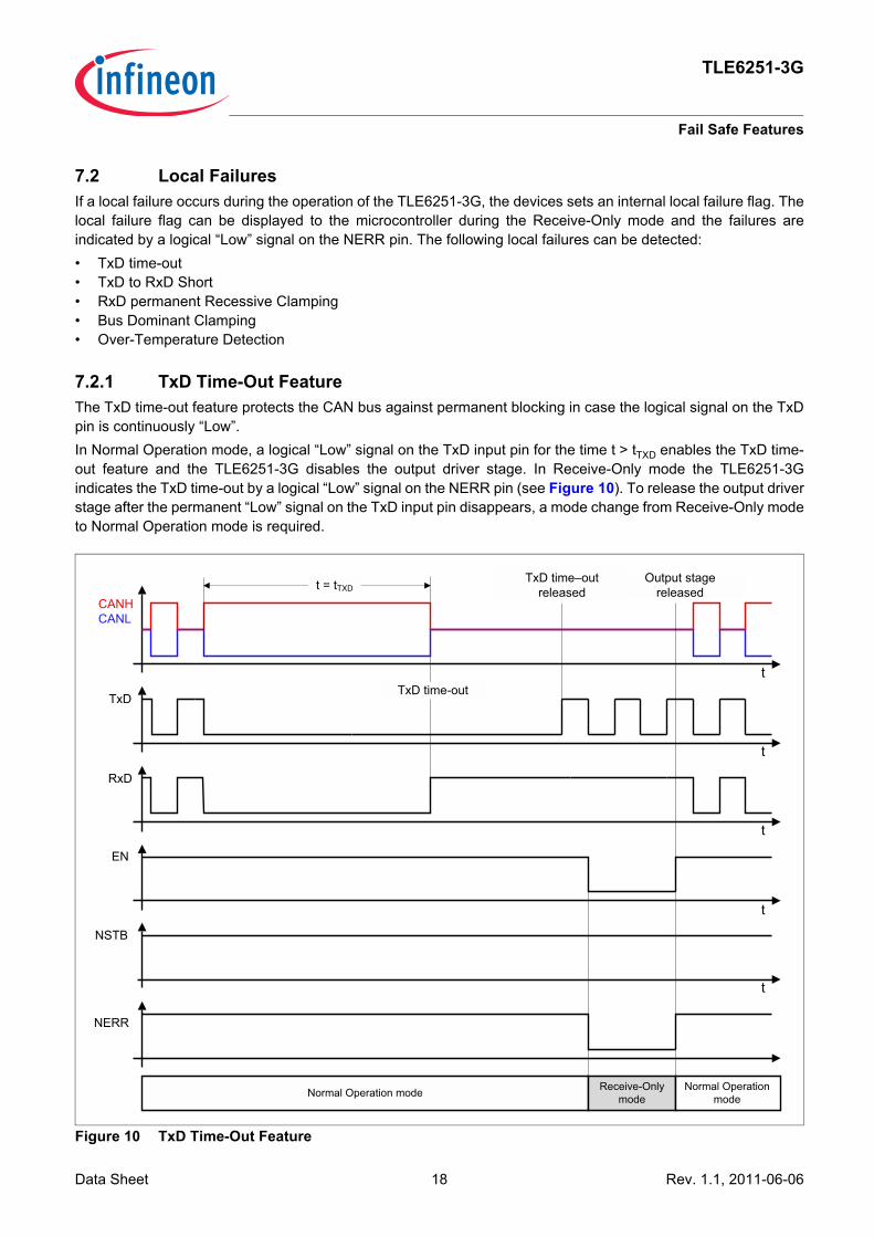
7.2.1 TxD Time-Out FeatureThe TxD time-out feature protects the CAN bus against permanent blocking in case the logical signal on the TxDpin is continuously “Low”. In Normal Operation mode, a logical “Low” signal on the TxD input pin for the time t > tTXD enables the TxD time-out feature and the TLE6251-3G disables the output driver stage. In Receive-Only mode the TLE6251-3Gindicates the TxD time-out by a logical “Low” signal on the NERR pin (see Figure 10). To release the output driverstage after the permanent “Low” signal on the TxD input pin disappears, a mode change from Receive-Only modeto Normal Operation mode is required.
Figure 10 TxD Time-Out Feature
TxD
t
CANHCANL
RxD
NSTB
t
TxD time-out
EN
NERR
Normal Operation mode Normal Operation mode
Receive-Only mode
TxD time–out released
Output stage released
t
t
t
t = tTXD
Data Sheet 18 Rev. 1.1, 2011-06-06

TLE6251-3G
Fail Safe Features
7.2.2 TxD to RxD Short Circuit FeatureA short between the pins TxD and RxD causes permanent blocking of the CAN bus. In the case, that the low sidedriver capability of the RxD output pin is stronger as the high side driver capability of the external microcontrolleroutput, which is connected to the TxD pin of the TLE6251-3G, the RxD output signal overrides the TxD signalprovided by the microcontroller. In this case a continuous “Dominant” signal blocks the CAN bus. The TLE6251-3G detects the short between the TxD and the RxD pin, disables the output driver stage and sets the internal localfailure flag. In Receive-Only mode the TLE6251-3G indicates the TxD to RxD short by a logical “Low” signal onthe NERR pin. The TLE6251-3G releases the failure flag and the output driver stage by an operation mode changefrom Receive-Only mode to Normal Operation mode.
7.2.3 RxD Permanent Recessive ClampingA logical “High” signal on the RxD pin indicates the external microcontroller, that there is no CAN message on theCAN bus. The microcontroller can transmit a message to the CAN bus only if the bus is recessive. In case thelogical “High” signal on the RxD pin is caused by a failure, like a short from RxD to VIO, the RxD signal doesn’tmirror the signal on the CAN bus. This allows the microcontroller to place a message to the CAN bus at any timeand corrupts CAN bus messages on the bus. The TLE6251-3G detects a permanent logical “High” signal on theRxD pin and set the local error flag. In order to avoid any data collisions on the CAN bus the output driver stagegets disabled. In Receive-Only mode the TLE6251-3G indicates the RxD Clamping by a logical “Low” signal onthe NERR pin. The TLE6251-3G releases the failure flag and the output driver stage by a operation mode changeor if the RxD clamping failure disappears.
7.2.4 Bus Dominant ClampingDue to a fail function on one of the CAN bus participants, the CAN bus could be permanent in “Dominant” state. Theexternal microcontroller doesn’t transmit any data to the CAN bus as long as the CAN bus remains “Dominant”. Evenif the permanent “Dominate” state on the CAN bus is caused by a short from CANH to VCC, or similar, the transceivercan not detect the failure, because the CAN bus failure detection works only when the transceiver is active sendingdata to the bus. Therefore the TLE6251-3G has a bus dominant clamping detection unit installed. In case the bussignal is “Dominant” for the time t > tBus,t the TLE6251-3G detects the bus clamping and sets the local failure flag.The output driver stage remains active. In Receive-Only mode the TLE6251-3G indicates the bus dominant clampingby a logical “Low” signal on the NERR pin.
Data Sheet 19 Rev. 1.1, 2011-06-06
TLE6251-3G
Fail Safe Features
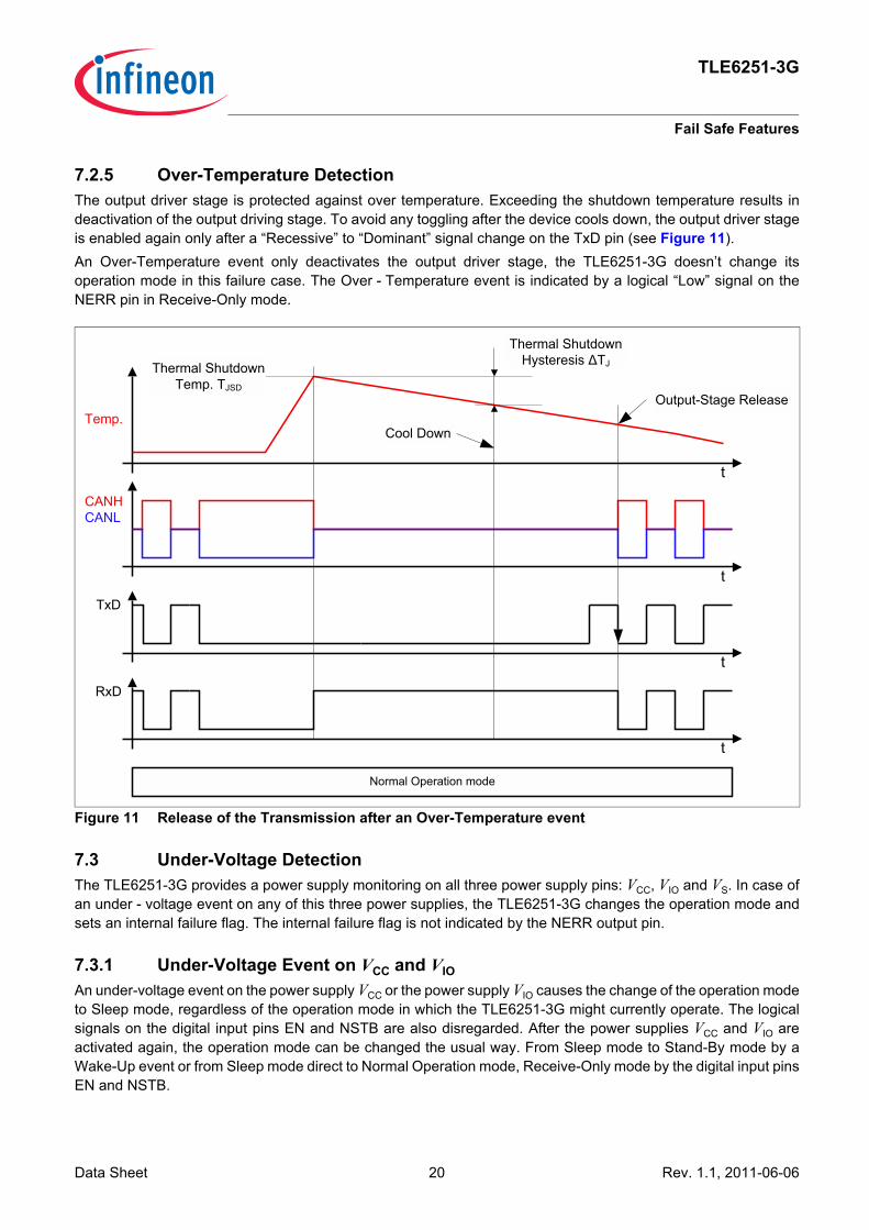
7.2.5 Over-Temperature DetectionThe output driver stage is protected against over temperature. Exceeding the shutdown temperature results indeactivation of the output driving stage. To avoid any toggling after the device cools down, the output driver stageis enabled again only after a “Recessive” to “Dominant” signal change on the TxD pin (see Figure 11).An Over-Temperature event only deactivates the output driver stage, the TLE6251-3G doesn’t change itsoperation mode in this failure case. The Over - Temperature event is indicated by a logical “Low” signal on theNERR pin in Receive-Only mode.
Figure 11 Release of the Transmission after an Over-Temperature event
7.3 Under-Voltage DetectionThe TLE6251-3G provides a power supply monitoring on all three power supply pins: VCC, VIO and VS. In case ofan under - voltage event on any of this three power supplies, the TLE6251-3G changes the operation mode andsets an internal failure flag. The internal failure flag is not indicated by the NERR output pin.
7.3.1 Under-Voltage Event on VCC and VIOAn under-voltage event on the power supply VCC or the power supply VIO causes the change of the operation modeto Sleep mode, regardless of the operation mode in which the TLE6251-3G might currently operate. The logicalsignals on the digital input pins EN and NSTB are also disregarded. After the power supplies VCC and VIO areactivated again, the operation mode can be changed the usual way. From Sleep mode to Stand-By mode by aWake-Up event or from Sleep mode direct to Normal Operation mode, Receive-Only mode by the digital input pinsEN and NSTB.
TxD
t
CANHCANL
RxD
Normal Operation mode
t
t
t
Temp.Output-Stage Release
Thermal Shutdown Temp. TJSD
Thermal Shutdown Hysteresis ΔTJ
Cool Down
Data Sheet 20 Rev. 1.1, 2011-06-06
TLE6251-3G
Fail Safe Features
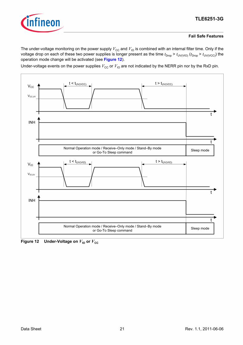
The under-voltage monitoring on the power supply VCC and VIO is combined with an internal filter time. Only if thevoltage drop on each of these two power supplies is longer present as the time tDrop > tUV(VIO) (tDrop > tUV(VCC)) theoperation mode change will be activated (see Figure 12).Under-voltage events on the power supplies VCC or VIO are not indicated by the NERR pin nor by the RxD pin.
Figure 12 Under-Voltage on VIO or VCC
INH
Normal Operation mode / Receive–Only mode / Stand–By mode or Go-To Sleep command
t
t
VCC
Sleep mode
VCC,UV
t < tUV(VCC) t > tUV(VCC)
INH
t
t
VIO
VIO,UV
t < tUV(VIO) t > tUV(VIO)
Normal Operation mode / Receive–Only mode / Stand–By mode or Go-To Sleep command Sleep mode
Data Sheet 21 Rev. 1.1, 2011-06-06

TLE6251-3G
Fail Safe Features
7.3.2 Under-Voltage Event on VSIf an under-voltage event is detected at the power supply VS, the TLE6251-3G immediately transfers into theStand-By mode, regardless of the operation mode in which the TLE6251-3G might currently operate. After thepower supply VS has been reestablished, the operation mode can be changed by applying a logical “High” signalto the EN pin or the NSTB pin. In the case the TLE6251-3G detects an under-voltage event on the VCC or VIO power supply, the TLE6251-3Gchanges to Sleep mode. If the TLE6251-3G detects in Sleep mode an under-voltage event on the VS power supply,the device changes to the Stand-By mode, even if the under-voltage event on the VCC or VIO power supply is stillpresent.
Figure 13 Under-Voltage on VS
7.4 Voltage AdaptationThe advantage of the adaptive microcontroller logic is the ratio metrical scaling of the I/O levels depending on theinput voltage at the VIO pin. Connecting the VIO input to the I/O supply of the microcontroller ensures, that the I/Ovoltage of the microcontroller fits to the internal logic levels of the TLE6251-3G.
t
VS
any mode
VS,Poff
VS,Pon
Power Down Stand-By mode
Data Sheet 22 Rev. 1.1, 2011-06-06

TLE6251-3G
Diagnosis-Flags at NERR and RxD
8 Diagnosis-Flags at NERR and RxD
Table 3 Truth TableNSTB EN INH Mode Event NERR RxD1 1 High Normal No CAN bus failure1)
1) Only valid after at least four recessive to dominant edges at TxD when entering the Normal Operation mode.
1 “Low”: bus dominant,“High”: bus recessive
CAN bus failure1) 0Wake-up via CAN bus/no wake-up request detected2)
2) Only valid before four recessive to dominant edges at TxD when entering the Normal Operation mode.
1
Wake-up via pin WK3)
3) Only valid before four recessive to dominant edges at TxD when entering the Normal Operation mode.
01 0 High Receive
OnlyNo VS fail detected4)
4) Power-Up flag only available, if VCC and VIO are active. Power-Up flag will be cleared when entering Normal Operation mode.
1 “Low”: bus dominant,“High”: bus recessive
VS fail detected4) 0No TxD time-out, Over-Temperature event,RxD recessive clamping or bus dominant time out detected5)
5) Valid after a transition from Normal Operation mode.
1
TxD time-out, Over-Temperature event,RxD recessive clamping or bus dominant time out detected5)
0
0 0 High Stand-By Wake-up request detected6)
6) Only valid if VCC and VIO are active.
0 0No Wake up request detected6) 1 1
0 0 Floating Sleep Wake-up request detected6) 0 0No wake-up request detected6) 1 1
Data Sheet 23 Rev. 1.1, 2011-06-06

TLE6251-3G
General Product Characteristics
9 General Product Characteristics
9.1 Absolute Maximum Ratings
Note: Stresses above the ones listed here may cause permanent damage to the device. Exposure to absolute maximum rating conditions for extended periods may affect device reliability.
Note: Integrated protection functions are designed to prevent IC destruction under fault conditions described in the data sheet. Fault conditions are considered as “outside” normal operating range. Protection functions are not designed for continuous repetitive operation.
Table 4 Absolute Maximum Ratings 1)
All voltages with respect to ground, positive current flowing into pin(unless otherwise specified)
1) Not subject to production test, specified by design.
Pos. Parameter Symbol Limit Values Unit ConditionsMin. Max.
Voltages9.1.1 Supply voltage VS -0.3 40 V –9.1.2 Transceiver supply voltage VCC -0.3 6.0 V –9.1.3 Logic supply voltage VIO -0.3 6.0 V –9.1.4 CANH DC voltage versus GND VCANH -40 40 V –9.1.5 CANL DC voltage versus GND VCANL -40 40 V –9.1.6 Input voltage at WK VWK -27 40 V –9.1.7 Input voltage at INH VINH -0.3 VS + 0.3 V –9.1.8 Differential voltage CANH to
CANLVDiff,CAN -40 40 V Max. differential voltage
between CAN and CANL
9.1.9 Logic voltages at EN, NSTB, NERR, TxD, RxD
VLogic -0.3 VIO V 0 V < VIO < 6.0 V
Currents9.1.10 Maximum Output Current INH IINH(max) -5 0 mA –Temperatures9.1.11 Junction Temperature Tj -40 150 °C –9.1.12 Storage Temperature Tstg -55 150 °C –ESD Susceptibility9.1.13 ESD Resistivity at CANH, CANL,
and WK versus GNDVESD -8 8 kV HBM2) (100 pF / 1.5 kΩ)
2) ESD susceptibility, HBM according to AEC-Q100-002D.
9.1.14 ESD Resistivity all other pins VESD -2 2 kV HBM2) (100 pF / 1.5 kΩ)
Data Sheet 24 Rev. 1.1, 2011-06-06

TLE6251-3G
General Product Characteristics
9.2 Functional Range
Note: Within the functional range the IC operates as described in the circuit description. The electrical characteristics are specified within the conditions given in the related electrical characteristics table.
9.3 Thermal Resistance
Table 5 Operating RangePos. Parameter Symbol Limit Values Unit Conditions
Min. Max.Supply Voltages9.2.1 Supply Voltage Range for
Normal OperationVS(nom) 5.5 18 V –
9.2.2 Extended Supply Voltage Range for Operation
VS(ext) 5.0 40 V Parameter Deviations possible
9.2.3 Transceiver Supply Voltage VCC 4.75 5.25 V –9.2.4 Logic Supply Voltage VIO 3.0 5.25 V –Thermal Parameters9.2.5 Junction temperature TJ -40 150 °C 1)
1) Not subject to production test, specified by design
Table 6 Thermal Characteristics1)
1) Not subject to production test, specified by design
Pos. Parameter Symbol Limit Values Unit ConditionsMin. Typ. Max.
Thermal Resistance9.3.1 Junction to Soldering Point1) RthJSP – – 25 K/W measured to pin 29.3.2 Junction to Ambient1) RthJA – 130 – K/W 2)
2) EIA/JESD 52_2, FR4, 80 × 80 × 1.5 mm; 35μ Cu, 5μ Sn; 300 mm2
Thermal Shutdown Junction Temperature9.3.3 Thermal shutdown temp. TJSD 150 175 190 °C – 9.3.4 Thermal shutdown hysteresis ΔT – 10 – K –
Data Sheet 25 Rev. 1.1, 2011-06-06
TLE6251-3G
Electrical Characteristics
10 Electrical Characteristics
10.1 Functional Device Characteristics
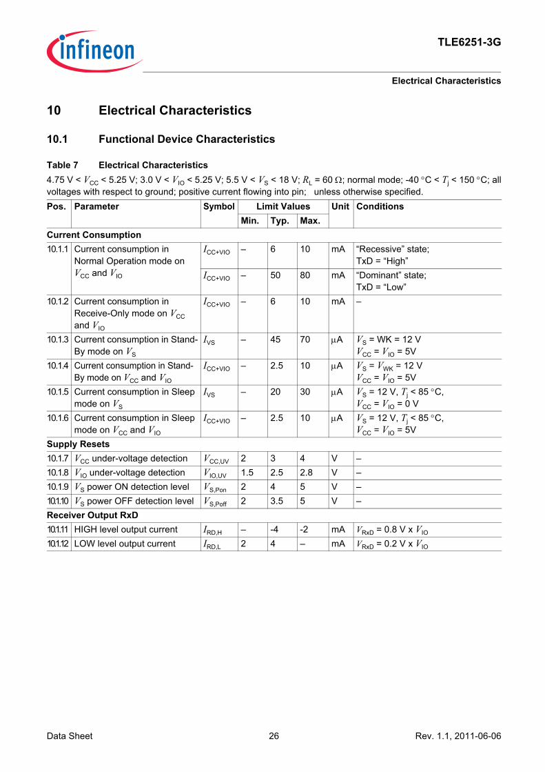
Table 7 Electrical Characteristics4.75 V < VCC < 5.25 V; 3.0 V < VIO < 5.25 V; 5.5 V < VS < 18 V; RL = 60 Ω; normal mode; -40 °C < Tj < 150 °C; allvoltages with respect to ground; positive current flowing into pin; unless otherwise specified.Pos. Parameter Symbol Limit Values Unit Conditions
Min. Typ. Max.Current Consumption10.1.1 Current consumption in
Normal Operation mode on VCC and VIO
ICC+VIO – 6 10 mA “Recessive” state; TxD = “High”
ICC+VIO – 50 80 mA “Dominant” state; TxD = “Low”
10.1.2 Current consumption in Receive-Only mode on VCC and VIO
ICC+VIO – 6 10 mA –
10.1.3 Current consumption in Stand-By mode on VS
IVS – 45 70 μA VS = WK = 12 V VCC = VIO = 5V
10.1.4 Current consumption in Stand-By mode on VCC and VIO
ICC+VIO – 2.5 10 μA VS = VWK = 12 VVCC = VIO = 5V
10.1.5 Current consumption in Sleep mode on VS
IVS – 20 30 μA VS = 12 V, Tj < 85 °C,VCC = VIO = 0 V
10.1.6 Current consumption in Sleep mode on VCC and VIO
ICC+VIO – 2.5 10 μA VS = 12 V, Tj < 85 °C,VCC = VIO = 5V
Supply Resets10.1.7 VCC under-voltage detection VCC,UV 2 3 4 V – 10.1.8 VIO under-voltage detection VIO,UV 1.5 2.5 2.8 V – 10.1.9 VS power ON detection level VS,Pon 2 4 5 V – 10.1.10 VS power OFF detection level VS,Poff 2 3.5 5 V – Receiver Output RxD10.1.11 HIGH level output current IRD,H – -4 -2 mA VRxD = 0.8 V x VIO
10.1.12 LOW level output current IRD,L 2 4 – mA VRxD = 0.2 V x VIO
Data Sheet 26 Rev. 1.1, 2011-06-06

TLE6251-3G
Electrical Characteristics
Transmission Input TxD10.1.13 High level input range VTD,H 0.7 ×
VIO
– VIO +0.3 V
V “Recessive” state
10.1.14 Low level input range VTD,L - 0.3 – 0.3 × VIO
V “Dominant” state
10.1.15 HIGH level input current ITD -5 0 5 μA VTxD = VIO 10.1.16 TxD pull-up resistance RTD 10 20 40 kΩ – Mode Control Inputs EN, NSTB10.1.17 High level input range VM,H 0.7 ×
VIO
– VIO +0.3 V
V “Recessive” state
10.1.18 Low level input range VM,L - 0.3 – 0.3 × VIO
V “Dominant” state
10.1.19 LOW level input current IMD -5 0 5 μA VEN and VNSTB = 0V 10.1.20 Pull-down resistance RM 50 100 200 kΩ –Diagnostic Output NERR10.1.21 HIGH level output voltage VNERR,H 0.8 ×
VIO
– – mA INERR = -100 μA
10.1.22 LOW level output voltage VNERR,L – – 0.2 ×VIO
mA INERR = 1.25 μA
Wake Input WK10.1.23 High Level voltage range at
WKVWK,H VS -
2 V– VS +
3 VV VEN = VNSTB = 0 V, rising edge
10.1.24 Low Level voltage range at WK VWK,L - 27 – VS - 4 V
V VEN = VNSTB = 0 V, falling edge
10.1.25 HIGH level input current IWKH -10 -5 – μA VWK = Vs - 2 V10.1.26 LOW level current IWKL – 5 10 μA VWK = Vs - 4 VInhibit Output INH10.1.27 HIGH level voltage drop
ΔVH = VS - VINH
ΔVH – 0.4 0.8 V IINH = -1 mA– 0.8 1.6 V 1)IINH = -5 mA
10.1.28 Leakage current IINH,lk – – 5 μA Sleep mode;VINH = 0 V
Table 7 Electrical Characteristics (cont’d)4.75 V < VCC < 5.25 V; 3.0 V < VIO < 5.25 V; 5.5 V < VS < 18 V; RL = 60 Ω; normal mode; -40 °C < Tj < 150 °C; allvoltages with respect to ground; positive current flowing into pin; unless otherwise specified.Pos. Parameter Symbol Limit Values Unit Conditions
Min. Typ. Max.
Data Sheet 27 Rev. 1.1, 2011-06-06
TLE6251-3G
Electrical Characteristics
Bus Transmitter10.1.29 CANL and CANH recessive
output voltageVCANL/H 2.0 – 3.0 V Normal Operation mode
no load 10.1.30 CANL and CANH recessive
output voltageVCANL/H -0.1 – 0.1 V Sleep or Stand-By mode
no load 10.1.31 CANH to CANL recessive
output voltage differenceVdiff -500 – 50 mV VTxD = VIO;
no load10.1.32 CANL dominant output voltage VCANL 0.5 – 2.25 V VTxD = 0 V; 50 Ω < RL < 65 Ω
10.1.33 CANH dominant output voltage
VCANH 2.75 – 4.5 V VTxD = 0 V;50 Ω < RL < 65 Ω
10.1.34 CANH, CANL dominant output voltage difference
Vdiff 1.5 – 3.0 V VTxD = 0 V; 50 Ω < RL < 65
10.1.35 CANL short circuit current ICANLsc 50 80 200 mA VCANLshort = 18 V10.1.36 CANH short circuit current ICANHsc -200 -80 -50 mA VCANHshort = 0 V
10.1.37 Leakage current ICANHL,lk -5 0 5 μA VS = VIO = VCC = 0 V;0 V < VCANH,L < 5 V
Bus Receiver10.1.38 Differential receiver input
range - Dominant Vdiff,rdN 0.9 – 5.0 V Normal Operation mode,
In respect to CMR10.1.39 Differential receiver input
range - Recessive Vdiff,drN -1.0 – 0.5 V Normal Operation mode,
In respect to CMR10.1.40 Differential receiver input
range - Dominant Vdiff,rdL 1.15 – 5.0 V Sleep mode, Stand-By mode
In respect to CMR10.1.41 Differential receiver input
range - Recessive Vdiff,drL -1.0 – 0.4 V Sleep mode, Stand-By mode
In respect to CMR10.1.42 Common mode range CMR -12 – 12 V VCC = 5 V 10.1.43 Differential receiver hysteresis Vdiff,hys – 100 – mV –10.1.44 CANH, CANL input resistance Ri 10 20 30 kΩ “Recessive” state10.1.45 Differential input resistance Rdiff 20 40 60 kΩ “Recessive” state
Table 7 Electrical Characteristics (cont’d)4.75 V < VCC < 5.25 V; 3.0 V < VIO < 5.25 V; 5.5 V < VS < 18 V; RL = 60 Ω; normal mode; -40 °C < Tj < 150 °C; allvoltages with respect to ground; positive current flowing into pin; unless otherwise specified.Pos. Parameter Symbol Limit Values Unit Conditions
Min. Typ. Max.
Data Sheet 28 Rev. 1.1, 2011-06-06
TLE6251-3G
Electrical Characteristics
Dynamic CAN-Transceiver Characteristics10.1.46 Propagation delay
TxD-to-RxD LOW (“Recessive” to “Dominant”)
td(L),TR – 150 255 ns CL = 100 pF;VCC = VIO = 5 V; CRxD = 15 pF
10.1.47 Propagation delayTxD-to-RxD HIGH (“Dominant” to “Recessive”)
td(H),TR – 150 255 ns CL = 100 pF;VCC = VIO = 5 V; CRxD = 15 pF
10.1.48 Propagation delayTxD LOW to bus “Dominant”
td(L),T – 50 120 ns CL = 100 pF;VCC = VIO = 5 V; CRxD = 15 pF
10.1.49 Propagation delayTxD HIGH to bus “Recessive”
td(H),T – 50 120 ns CL = 100 pF;VCC = VIO = 5 V; CRxD = 15 pF
10.1.50 Propagation delaybus “Dominant” to RxD “Low”
td(L),R – 100 135 ns CL = 100 pF;VCC = VIO = 5 V; CRxD = 15 pF
10.1.51 Propagation delaybus “Recessive” to RxD “High”
td(H),R – 100 135 ns CL = 100 pF;VCC = VIO = 5 V; CRxD = 15 pF
10.1.52 Min. hold time go to sleep command
thSLP 8 25 50 μs –
10.1.53 Min. wake-up time on pin WK tWK(local) 5 10 20 μs –10.1.54 Min. “Dominant” time for bus
wake-uptWake 0.75 3 5 μs –
10.1.55 TxD permanent “Dominant” disable time
tTxD 0.3 0.6 1.0 ms –
10.1.56 Bus permanent time-out tBus,t 0.3 0.6 1.0 ms –10.1.57 VCC, VµC undervoltage filter
timetUV(VIO)tUV(VCC)
200 320 480 ms –
10.1.58 Time for mode change tMode – 20 – μs 1)
1) Not subject to production test, specified by design.
Table 7 Electrical Characteristics (cont’d)4.75 V < VCC < 5.25 V; 3.0 V < VIO < 5.25 V; 5.5 V < VS < 18 V; RL = 60 Ω; normal mode; -40 °C < Tj < 150 °C; allvoltages with respect to ground; positive current flowing into pin; unless otherwise specified.Pos. Parameter Symbol Limit Values Unit Conditions
Min. Typ. Max.
Data Sheet 29 Rev. 1.1, 2011-06-06

TLE6251-3G
Electrical Characteristics
10.2 Diagrams
Figure 14 Test Circuit for Dynamic Characteristics
Figure 15 Timing Diagrams for Dynamic Characteristics
5
GND2
4
14
6
1
9WK
10
CANH
RL
VIO
NSTB
EN
TxD
RxD
3VCC
100nF
100nF
= =VCC
VS
100 nF
13
12CANL
CL
CRxD
VIO
td(L),Rt
VDIFF
td(L),TR
td(H),R
td(H),TR
td(L),Tt
GND
VTxD
VIO
td(H),T
0.9 V0.5 V
t
GND0.2 x VIO
0.8 x VIO
VRxD
VIO
Data Sheet 30 Rev. 1.1, 2011-06-06
TLE6251-3G
Application Information
11 Application InformationNote: The following information is given as a hint for the implementation of the device only and shall not be
regarded as a description or warranty of a certain functionality, condition or quality of the device.
11.1 Application Example
Figure 16 Application Circuit Example
ECU
ECU
Micro Controller
E.g. XC22xx
GND
TLE6251-3G
WK9
GND2
100nF
100nF
100nF
10 kΩ
CANH13
1)
51 µH
CANL12
VS
N.C.11
INH7
10
100nF
e.g. TLE 4476 (3.3/5 V) orTLE 4471TLE 4276TLE 4271
GND
VS
6
14
8
EN
NSTB
NERR4
RxD1
TxD5VIO
3VCC
VQ2
INH
VI1+ 22
µF+ 22
µF
5 V
100nF
+22µF
VQ1
STB8
RxD4
TxD1
3VCCGND
2
CANH7
1)
51 µH
CANL6
SPLIT5
e. g. TLE 4270VQVI
GND
Micro Controller
E.g. XC22xx
GND100nF
100nF
+ 22 µF
5 V
100nF
+22µF
60 Ω
CANBus
60 Ω
VBat
4.7 nF 1)
60 Ω 60 Ω4.7 nF 1)
1) Optional, according to the car manufacturer requirements
TLE6251DS
Data Sheet 31 Rev. 1.1, 2011-06-06
TLE6251-3G
Application Information
11.2 ESD Robustness according to IEC61000-4-2Test for ESD robustness according to IEC61000-4-2 “Gun test” (150 pF, 330 Ω) have been performed. The resultsand test conditions are available in a separate test report.
11.3 Voltage Drop over the INH Output
Figure 17 INH output voltage drop versus output current (typical values only!)
Table 8 ESD Robustness according to IEC61000-4-2Performed Test Result Unit RemarksElectrostatic discharge voltage at pin VS, CANH, CANL and WK versus GND
≥ 9 kV 1)Positive pulse
1) ESD susceptibility “ESD GUN” according to “Gift ICT Evaluation of CAN Transceiver “Section 4.3. (IEC 61000-4-2: 2001-12) -Tested by external test house (IBEE Zwickau, EMC Testreport Nr. 07a-04-09 referenced to the TLE6251-2G).
Electrostatic discharge voltage at pin VS, CANH, CANL and WK versus GND
≤ −9 kV 1)Negative pulse
Voltage Drop on the INH output pin
0,00
1,00
0,00 1,00 2,00 3,00 4,00 5,00
INH Output Current (mA)
Voltage Drop (V)
TJ = 150°C TJ = 25°C
TJ = -40°C
Data Sheet 32 Rev. 1.1, 2011-06-06

TLE6251-3G
Application Information
11.4 Mode Change to Sleep modeMode changes are applied either by a host command, an Wake-Up event or by an under-voltage event. To triggera mode change by a host command or in other words by a signal change on the digital input pins EN and NSTBall power supplies, VS VIO and VCC need to be available.TLE6251-3G.By setting the EN pin to logical “High” and the NSTB pin to logical “Low”, the TLE6251-3G enters the Go-To-Sleepcommand and after the time t = thSLP expires, the TLE6251-3G enters into the Sleep mode (see Chapter 5.5). Forany mode change, also for a mode change to Sleep mode the TLE6251-3G disregards the signal on the CAN bus.Therefore the TLE6251-3G can enter Sleep mode and remain in Sleep mode even if there is a short circuit on theCAN bus, for example CANH shorted to VS or VCC. In order to recognize a remote Wake-Up, the TLE6251-3G requires a signal change from “Recessive” to“Dominant” before the Wake-Up filter time starts (see Figure 6 and Figure 18).
Figure 18 Mode change to Sleep while the CANH bus is “Dominant”
11.5 Further Application Information• Please contact us for information regarding the pin FMEA.• Existing App. Note• For further information you may contact http://www.infineon.com/transceiver
CANHCANL
INH
t = tWake
Go-To Sleep command
Normal Operation mode
t
t
Sleep mode
no Wake-Up
Wake-Up
NSTB
EN
t
t
t = thSLP
„Recessive“ to „Dominant“ change
t = tWake
Stand-By mode
RxD
t
Data Sheet 33 Rev. 1.1, 2011-06-06
Data Sheet 34 Rev. 1.1, 2011-06-06
TLE6251-3G
Package Outlines
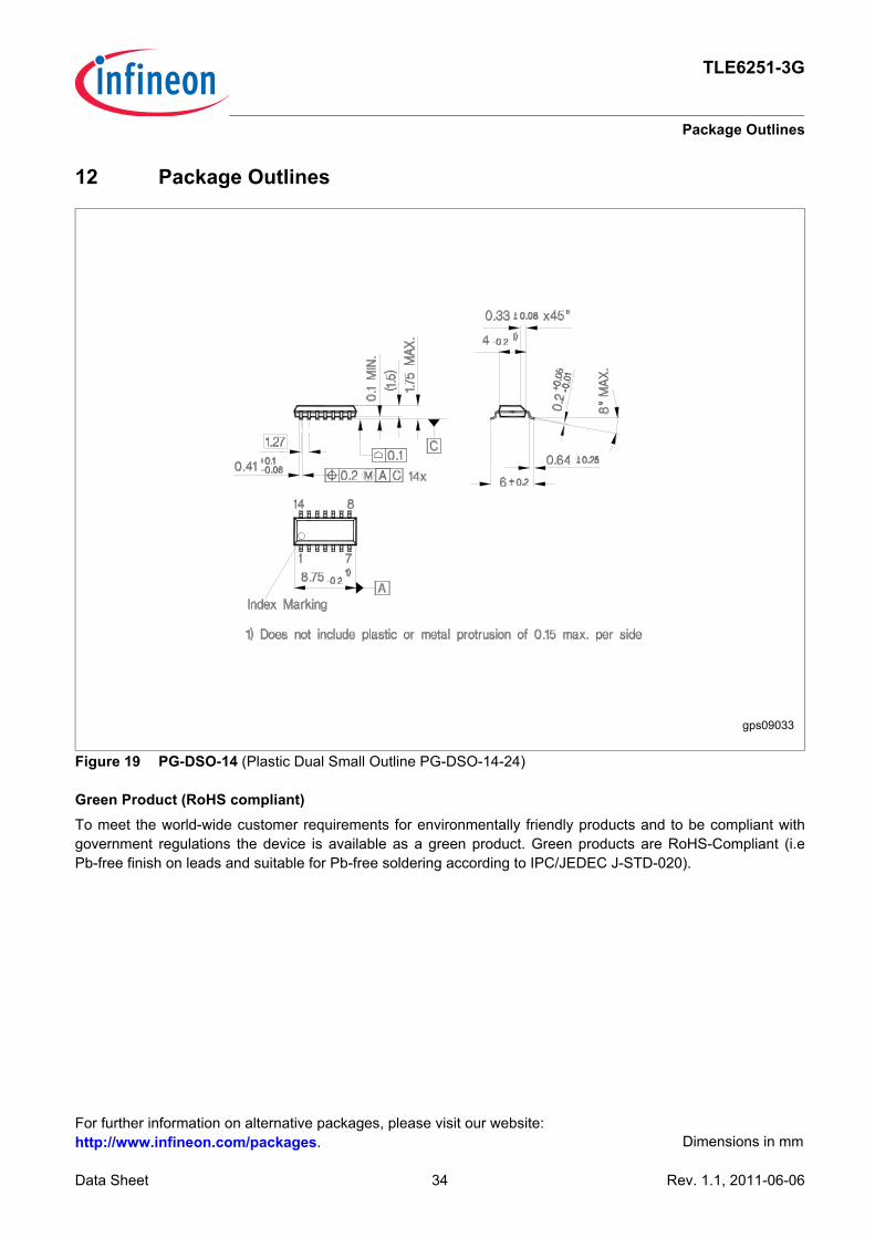
12 Package Outlines
Figure 19 PG-DSO-14 (Plastic Dual Small Outline PG-DSO-14-24)
Green Product (RoHS compliant)To meet the world-wide customer requirements for environmentally friendly products and to be compliant withgovernment regulations the device is available as a green product. Green products are RoHS-Compliant (i.ePb-free finish on leads and suitable for Pb-free soldering according to IPC/JEDEC J-STD-020).
gps09033
For further information on alternative packages, please visit our website: http://www.infineon.com/packages. Dimensions in mm
TLE6251-3G
Revision History
Data Sheet 35 Rev. 1.1, 2011-06-06
13 Revision HistoryRevision Date Changes1.1 2011-05-23 Update Data Sheet Rev.1.1 based on Data Sheet Rev. 1.0:
• All Pages:correct spelling and grammar.
• Update cover page, with new Infineon logo.• Page 7, Figure 3: updated.• Page 9, Figure 4: updated.• Page 18, Figure 10: updated.• Page 20, Figure 11, updated.• Page 22, Figure 13, updated.• Page 25, table 5, pos. 9.2.1:
New supply voltage range VS(Nom) from 5.5 V to 18 V.• Page 25, table 5, pos. 9.2.2:
New extended supply voltage range VS(Nom) from 5.0 V to 40 V.• Page 26ff, table 7, update table title:
New supply range 5.5 V < VS < 18 V.• Page 29, table 7, pos. 10.1.58:
Changed to typical value.• Page 30, Figure 15: updated.• Page 33, table 8:
Change algebraic sign of the negative pulse• Page 33:
Add new chapter 11.4

Edition 2011-06-06Published byInfineon Technologies AG81726 Munich, Germany© 2005 Infineon Technologies AGAll Rights Reserved.
Legal DisclaimerThe information given in this document shall in no event be regarded as a guarantee of conditions or characteristics. With respect to any examples or hints given herein, any typical values stated herein and/or any information regarding the application of the device, Infineon Technologies hereby disclaims any and all warranties and liabilities of any kind, including without limitation, warranties of non-infringement of intellectual property rights of any third party.
InformationFor further information on technology, delivery terms and conditions and prices, please contact the nearest Infineon Technologies Office (www.infineon.com).
WarningsDue to technical requirements, components may contain dangerous substances. For information on the types in question, please contact the nearest Infineon Technologies Office.Infineon Technologies components may be used in life-support devices or systems only with the express written approval of Infineon Technologies, if a failure of such components can reasonably be expected to cause the failure of that life-support device or system or to affect the safety or effectiveness of that device or system. Life support devices or systems are intended to be implanted in the human body or to support and/or maintain and sustain and/or protect human life. If they fail, it is reasonable to assume that the health of the user or other persons may be endangered.