tlv320aic3109-q1 automotive, low-power, 96-khz, … filters digital audio interface mix, mux audio...
TRANSCRIPT

Digital Filters
Digital Audio Interface
MIX, MUX
AudioADC
AudioDAC
DOUTBCLK
MIC1P/LINE1PMIC1M/LINE1M
MIC2P/LINE2PMIC2M/LINE2M
WCLKDIN
PGA
PGA_AUX
MIX, MUX
HPCOM
HPOUT
LEFT_LOP
RIGHT_LOM
LEFT_LOM
RIGHT_LOP
Product
Folder
Order
Now
Technical
Documents
Tools &
Software
Support &Community
ReferenceDesign
An IMPORTANT NOTICE at the end of this data sheet addresses availability, warranty, changes, use in safety-critical applications,intellectual property matters and other important disclaimers. PRODUCTION DATA.
TLV320AIC3109-Q1SLASE93A –AUGUST 2017–REVISED NOVEMBER 2017
TLV320AIC3109-Q1 Automotive, Low-Power, 96-kHz, Mono Audio Codec
1
1 Features1• Qualified for Automotive Applications• AEC-Q100 Qualified With the Following Results:
– Temperature Grade 2: –40°C to +105°C– HBM ESD Classification 2– CDM ESD Classification C4B
• Mono Audio DAC:– 102-dBA Signal-to-Noise Ratio– Supports Sample Rates From 8 kHz to 96 kHz– 3D, Bass, Treble, EQ, or De-Emphasis Effects
• Mono Audio ADC:– 92-dBA Signal-to-Noise Ratio– Supports Sample Rates From 8 kHz to 96 kHz– Digital Signal Processing and Noise Filtering
• Four Audio Input Pins:– Up to Two Differential Inputs– Up to Two Single-Ended Inputs
• Six Audio Output Drivers:– One Fully Differential or Two Single-Ended
Headphone Drivers– Mono Pair of Fully-Differential Line Outputs
• Low Power: 14-mW Mono, 48-kHz Playback With3.3-V Analog Supply
• Ultra-Low Power Mode With Passive AnalogBypass
• Front-End Programmable Gain Amplifier (PGA)• Programmable Digital Gain for DAC Playback• Automatic Gain Control (AGC) for Record• Programmable Microphone Bias• Programmable PLL for Flexible Clock Generation• I2C Control Bus• Audio Data Formats: I2S, Left- and Right-Justified,
DSP, and TDM• Power Supplies:
– Analog (AVDD, DRVDD): 2.7 V to 3.6 V– Digital Core (DVDD): 1.525 V to 1.95 V– Digital I/O (IOVDD): 1.1 V to 3.6 V
• Available in Two VQFN-32 Package Options:– Non-Wettable (6PAIC3109TRHBRQ1)– Wettable-Flank (6PAIC3109TWRHMRQ1)
2 Applications• Emergency Call (eCall) Systems• Telematics Control Unit (TCU)• Automotive Head Units
3 DescriptionThe TLV320AIC3109-Q1 device is a low-power monoaudio codec with a mono headphone amplifier andmultiple input and output channels that areprogrammable in single-ended or fully differentialconfigurations. The device includes extensiveregister-based power control, allowing 48-kHz digital-to-analog converter (DAC) playback at as little as14-mW consumption, making the device well-suitedfor low-power applications.
The record path of the TLV320AIC3109-Q1 containsintegrated microphone bias, a digitally controlledmicrophone preamplifier, automatic gain control(AGC), a flexible front-end multiplexer (MUX), and afront-end analog mixer (MIX). During record,programmable filters can remove audible noise. Theplayback path includes MIX and MUX capability fromthe mono DAC and selected inputs, throughprogrammable volume controls, to the variousoutputs.
Device Information(1)
PART NUMBER PACKAGE BODY SIZE (NOM)TLV320AIC3109-Q1 VQFN (32) 5.00 mm × 5.00 mm
(1) For all available packages, see the orderable addendum atthe end of the datasheet.
SPACE
Simplified Diagram

2
TLV320AIC3109-Q1SLASE93A –AUGUST 2017–REVISED NOVEMBER 2017 www.ti.com
Product Folder Links: TLV320AIC3109-Q1
Submit Documentation Feedback Copyright © 2017, Texas Instruments Incorporated
Table of Contents1 Features .................................................................. 12 Applications ........................................................... 13 Description ............................................................. 14 Revision History..................................................... 25 Pin Configuration and Functions ......................... 36 Specifications......................................................... 4
6.1 Absolute Maximum Ratings ...................................... 46.2 ESD Ratings.............................................................. 46.3 Recommended Operating Conditions....................... 56.4 Thermal Information .................................................. 56.5 Electrical Characteristics........................................... 66.6 Audio Data Serial Interface Timing Requirements.. 106.7 Typical Characteristics ............................................ 14
7 Detailed Description ............................................ 167.1 Overview ................................................................. 167.2 Functional Block Diagram ....................................... 167.3 Feature Description................................................. 177.4 Device Functional Modes........................................ 35
7.5 Programming........................................................... 387.6 Register Maps ......................................................... 40
8 Application and Implementation ...................... 1048.1 Application Information.......................................... 1048.2 Typical Application ................................................ 104
9 Power Supply Recommendations .................... 10710 Layout................................................................. 107
10.1 Layout Guidelines ............................................... 10710.2 Layout Example .................................................. 108
11 Device and Documentation Support ............... 10911.1 Documentation Support ...................................... 10911.2 Receiving Notification of Documentation
Updates.................................................................. 10911.3 Community Resources........................................ 10911.4 Trademarks ......................................................... 10911.5 Electrostatic Discharge Caution.......................... 10911.6 Glossary .............................................................. 109
12 Mechanical, Packaging, and OrderableInformation ......................................................... 109
4 Revision HistoryNOTE: Page numbers for previous revisions may differ from page numbers in the current version.
Changes from Original (August 2017) to Revision A Page
• Released 6PAIC3109TWRHMRQ1 (wettable-flank package option) to production............................................................... 1• Added TI Design to document ................................................................................................................................................ 1

32D
VD
D9
SD
A
1MCLK 24 DRVDD
31R
ES
ET
10M
IC1P
/LIN
E1P
2BCLK 23 HPOUT
30R
IGH
T_L
OM
11M
IC1M
/LIN
E1M
3WCLK 22 HPCOM
29R
IGH
T_L
OP
12M
IC2P
/LIN
E2P
4DIN 21 DRVSS
28LE
FT
_LO
M13
MIC
2M/L
INE
2M
5DOUT 20 NC
27LE
FT
_LO
P14
MIC
DE
T
6DVSS 19 NC
26A
VS
S15
MIC
BIA
S
7IOVDD 18 DRVDD
25A
VD
D16
NC
8SCL 17 AVSS
Not to scale
Thermal
Pad
3
TLV320AIC3109-Q1www.ti.com SLASE93A –AUGUST 2017–REVISED NOVEMBER 2017
Product Folder Links: TLV320AIC3109-Q1
Submit Documentation FeedbackCopyright © 2017, Texas Instruments Incorporated
5 Pin Configuration and Functions
RHB, RHM Packages32-Pin VQFN
Top View
NOTE: Connect the device thermal pad to DRVSS.
Pin FunctionsPIN
TYPE DESCRIPTIONNAME NO.
AVDD 25 — Analog DAC voltage supply; connect 1-µF and 0.1-µF decoupling capacitors in parallelto AVSS
AVSS 17, 26 — Analog groundBCLK 2 Digital I/O Audio serial data bus bit clock input/outputDIN 4 Digital input Audio serial data bus data inputDOUT 5 Digital output Audio serial data bus data output
DRVDD 18, 24 — Analog ADC and output driver voltage supply; connect 1-µF and 0.1-µF decouplingcapacitors in parallel to DRVSS
DRVSS 21 — Analog output driver ground supply
DVDD 32 — Digital core voltage supply; connect 1-µF and 0.1-µF decoupling capacitors in parallelto DVSS
DVSS 6 — Digital core and I/O ground supplyHPCOM 22 Analog output High-power output driver (single-ended output, differential output (–), or VCM output)HPOUT 23 Analog output High-power output driver, single-ended output or differential output (+)IOVDD 7 — Digital I/O voltage supplyLEFT_LOM 28 Analog output Left line output (–); leave floating when not usedLEFT_LOP 27 Analog output Left line output (+); leave floating when not used

4
TLV320AIC3109-Q1SLASE93A –AUGUST 2017–REVISED NOVEMBER 2017 www.ti.com
Product Folder Links: TLV320AIC3109-Q1
Submit Documentation Feedback Copyright © 2017, Texas Instruments Incorporated
Pin Functions (continued)PIN
TYPE DESCRIPTIONNAME NO.MCLK 1 Digital input Master clock input
MIC1M/LINE1M 11 Analog input Microphone or line input, differential only (–); connect a 0.47-µF capacitor to AVSSwhen not used
MIC1P/LINE1P 10 Analog input Microphone or line input, differential (+) or single-ended; connect a 0.47-µF capacitor toAVSS when not used
MIC2M/LINE2M 13 Analog input Microphone or line input, differential only (–); connect a 0.47-µF capacitor to AVSSwhen not used
MIC2P/LINE2P 12 Analog input Microphone or line input, differential (+) or single-ended; connect a 0.47-µF capacitor toAVSS when not used
MICDET 14 Analog input Microphone detection input; leave floating when not usedNC 16, 19, 20 — Not connected; always leave floatingMICBIAS 15 Analog output Microphone bias voltage output; leave floating when not usedRESET 31 Digital input ResetRIGHT_LOM 30 Analog output Right line output (–); leave floating when not usedRIGHT_LOP 29 Analog output Right line output (+); leave floating when not usedSCL 8 Digital I/O I2C serial clock inputSDA 9 Digital I/O I2C serial data input/outputWCLK 3 Digital I/O Audio serial data bus word clock input/output
(1) Stresses beyond those listed under Absolute Maximum Ratings may cause permanent damage to the device. These are stress ratingsonly, which do not imply functional operation of the device at these or any other conditions beyond those indicated under RecommendedOperating Conditions. Exposure to absolute-maximum-rated conditions for extended periods may affect device reliability.
(2) ESD compliance tested to EIA/JESD22-A114-B and passed.
6 Specifications
6.1 Absolute Maximum RatingsMIN MAX UNIT
Power-supply voltage
AVDD to AVSS, DRVDD to DRVSS –0.3 3.9
VAVDD to DRVSS –0.3 3.9IOVDD to DVSS –0.3 3.9DVDD to DVSS –0.3 2.5AVDD to DRVDD –0.1 0.1
Analog input voltage Analog input voltage to AVSS –0.3 AVDD + 0.3 VDigital input voltage Digital input voltage to DVSS –0.3 IOVDD + 0.3 V
TemperatureOperating ambient, TA –40 105
°CJunction, TJ –40 125Storage, Tstg –40 150
(1) AEC Q100-002 indicates that HBM stressing shall be in accordance with the ANSI/ESDA/JEDEC JS-001 specification.
6.2 ESD RatingsVALUE UNIT
V(ESD) Electrostatic discharge
Human-body model (HBM), per AEC Q100-002 (1) ±2000
VCharged-device model (CDM),per AEC Q100-011
Corner pins(1, 8, 9, 16,17, 24, 25, 32) ±750
All other pins ±500

5
TLV320AIC3109-Q1www.ti.com SLASE93A –AUGUST 2017–REVISED NOVEMBER 2017
Product Folder Links: TLV320AIC3109-Q1
Submit Documentation FeedbackCopyright © 2017, Texas Instruments Incorporated
6.3 Recommended Operating ConditionsMIN NOM MAX UNIT
POWER SUPPLYAnalog supply voltage (AVDD to AVSS, DRVDD to DRVSS) 2.7 3.3 3.6 VDigital core supply voltage (DVDD to DVSS) 1.525 1.8 1.95 VDigital I/O supply voltage (IOVDD to DVSS) 1.1 1.8 3.6 V
ANALOG INPUTSVI Analog full-scale, 0-dB input voltage (DRVDD = 3.3 V) 0.707 VRMS
DIGITAL INPUTSVDIG Digital input voltage DVSS IOVDD VTEMPERATURETA Operating free-air temperature –40 105 °COTHERS
Mono line output load resistance 10 kΩMono headphone output load resistance 16 ΩDigital output load capacitance 10 pF
(1) For more information about traditional and new thermal metrics, see the Semiconductor and IC Package Thermal Metrics applicationreport.
6.4 Thermal Information
THERMAL METRIC (1)TLV320AIC3109-Q1
UNITRHB (VQFN) RHM (VQFN)32 PINS 32 PINS
RθJA Junction-to-ambient thermal resistance 31.1 31.3 °C/WRθJC(top) Junction-to-case (top) thermal resistance 19.5 18.9 °C/WRθJB Junction-to-board thermal resistance 10.6 11.1 °C/WψJT Junction-to-top characterization parameter 0.2 0.2 °C/WψJB Junction-to-board characterization parameter 10.6 11.1 °C/WRθJC(bot) Junction-to-case (bottom) thermal resistance 0.9 0.9 °C/W

6
TLV320AIC3109-Q1SLASE93A –AUGUST 2017–REVISED NOVEMBER 2017 www.ti.com
Product Folder Links: TLV320AIC3109-Q1
Submit Documentation Feedback Copyright © 2017, Texas Instruments Incorporated
(1) Ratio of output level with 1-kHz, full-scale, sine-wave input to the output level with the inputs short-circuited, measured A-weighted overa 20-Hz to 20-kHz bandwidth using an audio analyzer.
(2) All performance measurements done with 20-kHz, low-pass filter and an A-weighted filter, where noted. Failure to use such a filter mayresult in higher THD+N and lower SNR and dynamic range readings than shown in the Electrical Characteristics. The low-pass filterremoves out-of-band noise, which, although not audible, may affect dynamic specification values.
6.5 Electrical Characteristicsat 25°C, AVDD = DRVDD = IOVDD = 3.3 V, DVDD = 1.8 V, fS = 48 kHz, and 16-bit audio data (unless otherwise noted)
PARAMETER TEST CONDITIONS MIN TYP MAX UNITAUDIO ADC
Input signal level Single-ended configurations 0.707 VRMS
SNR Signal-to-noise ratio (1) (2) A-weighted, fS = 48 kSPS, 0-dB PGA gain,inputs ac-shorted to ground 80 92 dB
DR Dynamic range (1) (2) fS = 48 kSPS; 0-dB PGA gain; 1-kHz, –60-dB,full-scale input signal 93 dB
THD Total harmonic distortion fS = 48 kSPS; 0-dB PGA gain; 1-kHz, –2-dB,full-scale input signal –89 –75 dB
PSRR Power-supply rejection ratio217-Hz signal applied to DRVDD 55
dB1-kHz signal applied to DRVDD 44
Input channel separation 1-kHz, –2-dB, full-scale signal, MIC1 to MIC2 –71 dB
Gain error fS = 48 kSPS; 0-dB PGA gain; 1-kHz, –2-dB,full-scale input signal 0.82 dB
ADC programmable-gainamplifier maximum gain 1-kHz input tone 59.5 dB
ADC programmable-gainamplifier step size 0.5 dB
Input resistance
MIC1/MIC2 inputs routed to single ADCinput MIX attenuation = 0 dB 20
kΩMIC1/MIC2 inputs routed to single ADCinput MIX attenuation = 12 dB 80
Input resistance 80 kΩInput capacitance MIC1/LINE1 inputs 10 pFInput level control minimumattenuation setting 0 dB
Input level control maximumattenuation setting 12 dB
Input level control attenuationstep size 1.5 dB
ANALOG PASSTHROUGH MODERDS(on) Input-to-output switch resistance MIC1/LINE1 to LINEOUT 330 ΩINPUT SIGNAL LEVEL, DIFFERENTIAL
SNR Signal-to-noise ratio A-weighted, fS = 48 kSPS, 0-dB PGA gain,inputs ac-shorted to ground 92 dB
THD Total harmonic distortion fS = 48 kHz; 0-dB PGA gain, 1-kHz, –2-dB,full-scale input signal –94 dB
ADC DIGITAL DECIMATION FILTER (fS = 48 kHz)
Filter gain
From 0 fS to 0.39 fS ±0.1
dBAt 0.4125 fS –0.25At 0.45 fS –3At 0.5 fS –17.5From 0.55 fS to 64 fS –75
Filter group delay 17/fS s
7
TLV320AIC3109-Q1www.ti.com SLASE93A –AUGUST 2017–REVISED NOVEMBER 2017
Product Folder Links: TLV320AIC3109-Q1
Submit Documentation FeedbackCopyright © 2017, Texas Instruments Incorporated
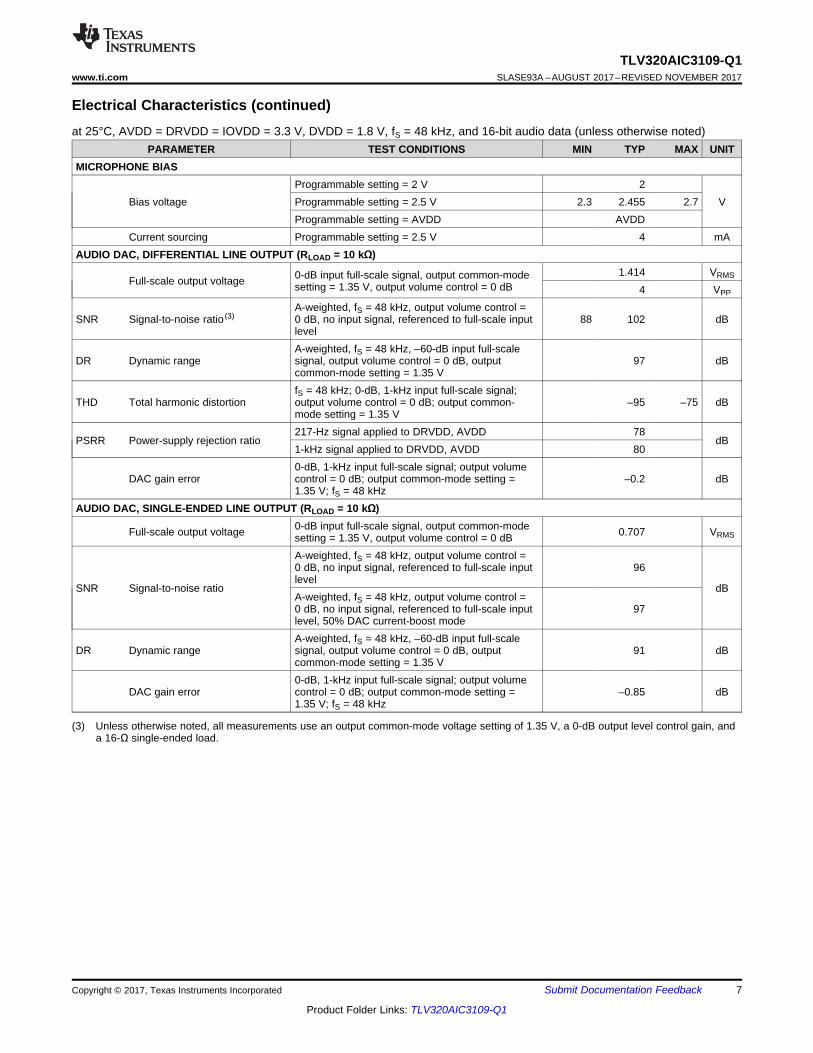
Electrical Characteristics (continued)at 25°C, AVDD = DRVDD = IOVDD = 3.3 V, DVDD = 1.8 V, fS = 48 kHz, and 16-bit audio data (unless otherwise noted)
PARAMETER TEST CONDITIONS MIN TYP MAX UNIT
(3) Unless otherwise noted, all measurements use an output common-mode voltage setting of 1.35 V, a 0-dB output level control gain, anda 16-Ω single-ended load.
MICROPHONE BIAS
Bias voltageProgrammable setting = 2 V 2
VProgrammable setting = 2.5 V 2.3 2.455 2.7Programmable setting = AVDD AVDD
Current sourcing Programmable setting = 2.5 V 4 mAAUDIO DAC, DIFFERENTIAL LINE OUTPUT (RLOAD = 10 kΩ)
Full-scale output voltage 0-dB input full-scale signal, output common-modesetting = 1.35 V, output volume control = 0 dB
1.414 VRMS
4 VPP
SNR Signal-to-noise ratio (3)A-weighted, fS = 48 kHz, output volume control =0 dB, no input signal, referenced to full-scale inputlevel
88 102 dB
DR Dynamic rangeA-weighted, fS = 48 kHz, –60-dB input full-scalesignal, output volume control = 0 dB, outputcommon-mode setting = 1.35 V
97 dB
THD Total harmonic distortionfS = 48 kHz; 0-dB, 1-kHz input full-scale signal;output volume control = 0 dB; output common-mode setting = 1.35 V
–95 –75 dB
PSRR Power-supply rejection ratio217-Hz signal applied to DRVDD, AVDD 78
dB1-kHz signal applied to DRVDD, AVDD 80
DAC gain error0-dB, 1-kHz input full-scale signal; output volumecontrol = 0 dB; output common-mode setting =1.35 V; fS = 48 kHz
–0.2 dB
AUDIO DAC, SINGLE-ENDED LINE OUTPUT (RLOAD = 10 kΩ)
Full-scale output voltage 0-dB input full-scale signal, output common-modesetting = 1.35 V, output volume control = 0 dB 0.707 VRMS
SNR Signal-to-noise ratio
A-weighted, fS = 48 kHz, output volume control =0 dB, no input signal, referenced to full-scale inputlevel
96
dBA-weighted, fS = 48 kHz, output volume control =0 dB, no input signal, referenced to full-scale inputlevel, 50% DAC current-boost mode
97
DR Dynamic rangeA-weighted, fS = 48 kHz, –60-dB input full-scalesignal, output volume control = 0 dB, outputcommon-mode setting = 1.35 V
91 dB
DAC gain error0-dB, 1-kHz input full-scale signal; output volumecontrol = 0 dB; output common-mode setting =1.35 V; fS = 48 kHz
–0.85 dB

8
TLV320AIC3109-Q1SLASE93A –AUGUST 2017–REVISED NOVEMBER 2017 www.ti.com
Product Folder Links: TLV320AIC3109-Q1
Submit Documentation Feedback Copyright © 2017, Texas Instruments Incorporated
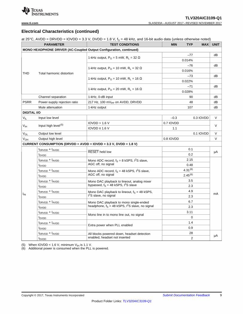
Electrical Characteristics (continued)at 25°C, AVDD = DRVDD = IOVDD = 3.3 V, DVDD = 1.8 V, fS = 48 kHz, and 16-bit audio data (unless otherwise noted)
PARAMETER TEST CONDITIONS MIN TYP MAX UNIT
(4) Ratio of output level with a 1-kHz, full-scale input to the output level playing an all-zero signal, measured A-weighted over a 20-Hz to20-kHz bandwidth.
AUDIO DAC, SINGLE-ENDED HEADPHONE OUTPUT (RLOAD = 16 Ω)
Full-scale output voltage 0-dB input full-scale signal, output common-modesetting = 1.35 V, output volume control = 0 dB 0.707 VRMS
SNR Signal-to-noise ratio
A-weighted, fS = 48 kHz, output volume control =0 dB, no input signal, referenced to full-scale inputlevel
96
dBA-weighted, fS = 48 kHz, output volume control =0 dB, no input signal, referenced to full-scale inputlevel, 50% DAC current-boost mode
97
DR Dynamic rangeA-weighted, fS = 48 kHz, –60-dB input full-scalesignal, output volume control = 0 dB, outputcommon-mode setting = 1.35 V
91 dB
THD Total harmonic distortionfS = 48 kHz, 0-dB input full-scale signal, outputvolume control = 0 dB, output common-modesetting = 1.35 V
–71 –65 dB
PSRR Power-supply rejection ratio217-Hz signal applied to DRVDD, AVDD 43
dB1-kHz signal applied to DRVDD, AVDD 41
DAC gain error0-dB, 1-kHz input full-scale signal; output volumecontrol = 0 dB; output common-mode setting =1.35 V; fS = 48 kHz
–0.85 dB
DAC DIGITAL INTERPOLATION FILTER (fS = 48 kHz)Pass band 0 0.45 fS HzPass-band ripple ±0.06 dBTransition band 0.45 fS 0.55 fS HzStop band 0.55 fS 7.5 fS HzStop-band attenuation 65 dBGroup delay 21 / fS s
MONO HEADPHONE DRIVER (AC-Coupled Output Configuration (3))
0-dB full-scale output voltage 0-dB gain to high-power outputs, output common-mode voltage setting = 1.35 V 0.707 VRMS
Programmable output common-mode voltage (applicable to lineoutputs also)
First option 1.35
VSecond option 1.5Third option 1.65Fourth option 1.8
Maximum programmable outputlevel control gain 9 dB
Programmable output levelcontrol gain step size 1 dB
PO Maximum output powerRL = 32 Ω 15
mWRL = 16 Ω 30
SNR Signal-to-noise ratio (4) A-weighted 94 dB
9
TLV320AIC3109-Q1www.ti.com SLASE93A –AUGUST 2017–REVISED NOVEMBER 2017
Product Folder Links: TLV320AIC3109-Q1
Submit Documentation FeedbackCopyright © 2017, Texas Instruments Incorporated
Electrical Characteristics (continued)at 25°C, AVDD = DRVDD = IOVDD = 3.3 V, DVDD = 1.8 V, fS = 48 kHz, and 16-bit audio data (unless otherwise noted)
PARAMETER TEST CONDITIONS MIN TYP MAX UNIT
(5) When IOVDD < 1.6 V, minimum VIH is 1.1 V.(6) Additional power is consumed when the PLL is powered.
MONO HEADPHONE DRIVER (AC-Coupled Output Configuration, continued)
THD Total harmonic distortion
1-kHz output, PO = 5 mW, RL = 32 Ω–77 dB
0.014%
1-kHz output, PO = 10 mW, RL = 32 Ω–76 dB
0.016%
1-kHz output, PO = 10 mW, RL = 16 Ω–73 dB
0.022%
1-kHz output, PO = 20 mW, RL = 16 Ω–71 dB
0.028%Channel separation 1-kHz, 0-dB input 90 dB
PSRR Power-supply rejection ratio 217 Hz, 100 mVPP on AVDD, DRVDD 48 dBMute attenuation 1-kHz output 107 dB
DIGITAL I/OVIL Input low level –0.3 0.3 IOVDD V
VIH Input high level (5) IOVDD > 1.6 V 0.7 IOVDDV
IOVDD ≤ 1.6 V 1.1VOL Output low level 0.1 IOVDD VVOH Output high level 0.8 IOVDD VCURRENT CONSUMPTION (DRVDD = AVDD = IOVDD = 3.3 V, DVDD = 1.8 V)
IIN
IDRVDD + IAVDD RESET held low0.1
µAIDVDD 0.2IDRVDD + IAVDD Mono ADC record, fS = 8 kSPS, I2S slave,
AGC off, no signal2.15
mA
IDVDD 0.48IDRVDD + IAVDD Mono ADC record, fS = 48 kSPS, I2S slave,
AGC off, no signal4.31 (6)
IDVDD 2.45 (6)
IDRVDD + IAVDD Mono DAC playback to lineout, analog mixerbypassed, fS = 48 kSPS, I2S slave
3.5IDVDD 2.3IDRVDD + IAVDD Mono DAC playback to lineout, fS = 48 kSPS,
I2S slave, no signal4.9
IDVDD 2.3IDRVDD + IAVDD Mono DAC playback to mono single-ended
headphone, fS = 48 kSPS, I2S slave, no signal6.7
IDVDD 2.3IDRVDD + IAVDD Mono line in to mono line out, no signal
3.11IDVDD 0IDRVDD + IAVDD Extra power when PLL enabled
1.4IDVDD 0.9IDRVDD + IAVDD All blocks powered down, headset detection
enabled, headset not inserted28
µAIDVDD 2

10
TLV320AIC3109-Q1SLASE93A –AUGUST 2017–REVISED NOVEMBER 2017 www.ti.com
Product Folder Links: TLV320AIC3109-Q1
Submit Documentation Feedback Copyright © 2017, Texas Instruments Incorporated
(1) All timing specifications are measured at characterization but not tested at final test.(2) All specifications at 25°C, DVDD = 1.8 V.
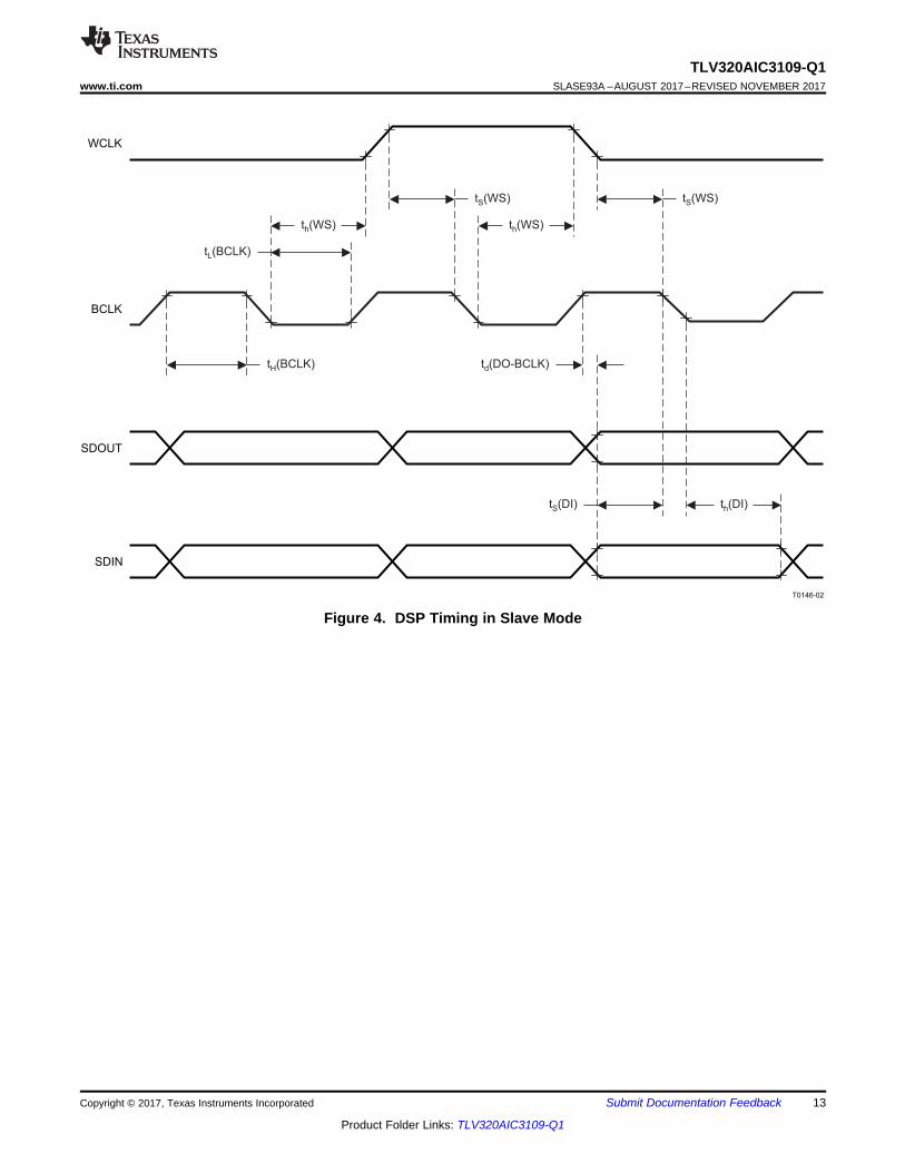
6.6 Audio Data Serial Interface Timing Requirements (1) (2)
IOVDD = 1.1 V IOVDD = 3.3 VUNIT
MIN MAX MIN MAXI2S, LEFT-JUSTIFIED AND RIGHT-JUSTIFIED TIMING IN MASTER MODE (See Figure 1)td(WS) ADWS, WCLK delay time 50 15 nstd(DO-WS) ADWS, WCLK to DOUT delay time 50 20 nstd(DO-BCLK) BCLK to DOUT delay time 50 15 nsts(DI) DIN setup time 10 6 nsth(DI) DIN hold time 10 6 nstr Rise time 30 10 nstf Fall time 30 10 nsDSP TIMING IN MASTER MODE (See Figure 2)td(WS) ADWS, WCLK delay time 50 15 nstd(DO-BCLK) BCLK to DOUT delay time 50 15 nsts(DI) DIN setup time 10 6 nsth(DI) DIN hold time 10 6 nstr Rise time 30 10 nstf Fall time 30 10 nsI2S, LEFT-JUSTIFIED AND RIGHT-JUSTIFIED TIMING IN SLAVE MODE (See Figure 3)tH(BCLK) BCLK high period 70 35 nstL(BCLK) BCLK low period 70 35 nsts(WS) ADWS, WCLK setup time 10 6 nsth(WS) ADWS, WCLK hold time 10 6 nstd(DO-WS) ADWS, WCLK to DOUT delay time (for left-justified mode only) 50 35 nstd(DO-BCLK) BCLK to DOUT delay time 50 20 nsts(DI) DIN setup time 10 6 nsth(DI) DIN hold time 10 6 nstr Rise time 8 4 nstf Fall time 8 4 nsDSP TIMING IN SLAVE MODE (See Figure 4)tH(BCLK) BCLK high period 70 35 nstL(BCLK) BCLK low period 70 35 nsts(WS) ADWS, WCLK setup time 10 8 nsth(WS) ADWS, WCLK hold time 10 8 nstd(DO-BCLK) BCLK to DOUT delay time 50 20 nsts(DI) DIN setup time 10 6 nsth(DI) DIN hold time 10 6 nstr Rise time 8 4 nstf Fall time 8 4 ns

T0146-01
WCLK
BCLK
SDOUT
SDIN
t (DO-BCLK)d
t (WS)d t (WS)d
t (DI)S t (DI)h
T0145-01
WCLK
BCLK
SDOUT
SDIN
t (DO-BCLK)dt (DO-WS)d
t (WS)d
t (DI)S t (DI)h
11
TLV320AIC3109-Q1www.ti.com SLASE93A –AUGUST 2017–REVISED NOVEMBER 2017
Product Folder Links: TLV320AIC3109-Q1
Submit Documentation FeedbackCopyright © 2017, Texas Instruments Incorporated
Figure 1. I2S, Left-Justified and Right-Justified Format Timing in Master Mode
Figure 2. DSP Timing in Master Mode

T0145-02
WCLK
BCLK
SDOUT
SDIN
t (WS)h
t (BCLK)H
t (DO-BCLK)d
t (DO-WS)d
t (DI)S
t (BCLK)L
t (DI)h
t (WS)S
12
TLV320AIC3109-Q1SLASE93A –AUGUST 2017–REVISED NOVEMBER 2017 www.ti.com
Product Folder Links: TLV320AIC3109-Q1
Submit Documentation Feedback Copyright © 2017, Texas Instruments Incorporated
Figure 3. I2S, Left-Justified and Right-Justified Format Timing in Slave Mode
T0146-02
WCLK
BCLK
SDOUT
SDIN
t (WS)h t (WS)h
t (BCLK)L
t (DO-BCLK)d
t (DI)S
t (BCLK)H
t (DI)h
t (WS)S t (WS)S
13
TLV320AIC3109-Q1www.ti.com SLASE93A –AUGUST 2017–REVISED NOVEMBER 2017
Product Folder Links: TLV320AIC3109-Q1
Submit Documentation FeedbackCopyright © 2017, Texas Instruments Incorporated
Figure 4. DSP Timing in Slave Mode
PGA Setting (dB)
Gai
n E
rror
(dB
)
0 10 20 30 40 50 60 700.5
0.55
0.6
0.65
0.7
0.75
0.8
0.85
ADC1.8
2.0
2.2
2.4
2.6
2.8
3.0
3.2
3.4
3.6
AVDD - Supply Voltage - V
MIC
BIA
S O
utp
utV
oltage
-V
G007
MICBIAS = AVDD
MICBIAS = 2.5 V
MICBIAS = 2 V
2.7 2.8 2.9 3.0 3.1 3.2 3.3 3.4 3.5 3.6
24
26
28
30
32
34
36
38
40
42
PGA Gain Setting − dB
SN
R−
Sig
nal-to
-Nois
e R
atio
−dB
G006
0 10 20 30 40 50 60
f − Frequency − kHz
−160
−140
−120
−100
−80
−60
−40
−20
0
Am
plit
ude
−dB
G004
0 2 4 6 8 10 12 14 16 18 20
f − Frequency − kHz
−160
−140
−120
−100
−80
−60
−40
−20
0
Am
plit
ude
−dB
G003
0 2 4 6 8 10 12 14 16 18 20
Headphone Power (mW)
Tot
al H
arm
onic
Dis
tort
ion
(dB
)
0 10 20 30 40 50 60 70 80 90 100-80
-70
-60
-50
-40
-30
-20
-10
0HPOUT DRVDD = 2.7 VHPOUT DRVDD = 3.3 VHPOUT DRVDD = 3.6 V
14
TLV320AIC3109-Q1SLASE93A –AUGUST 2017–REVISED NOVEMBER 2017 www.ti.com
Product Folder Links: TLV320AIC3109-Q1
Submit Documentation Feedback Copyright © 2017, Texas Instruments Incorporated
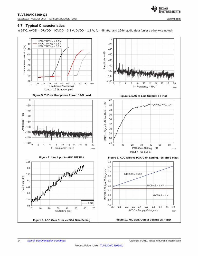
6.7 Typical Characteristicsat 25°C, AVDD = DRVDD = IOVDD = 3.3 V, DVDD = 1.8 V, fS = 48 kHz, and 16-bit audio data (unless otherwise noted)
Load = 16 Ω, ac-coupled
Figure 5. THD vs Headphone Power, 16-Ω Load Figure 6. DAC to Line Output FFT Plot
Figure 7. Line Input to ADC FFT Plot
Input = –65 dBFS
Figure 8. ADC SNR vs PGA Gain Setting, –65-dBFS Input
Figure 9. ADC Gain Error vs PGA Gain Setting Figure 10. MICBIAS Output Voltage vs AVDD

1.8
2.0
2.2
2.4
2.6
2.8
3.0
3.2
TA - Ambient Temperature - C°
MIC
BIA
S O
utp
utV
oltage -
V
G008
MICBIAS = AVDD
MICBIAS = 2.5 V
MICBIAS = 2 V
-45 -35 -25 -15 -5 5 15 25 35 45 55 65 75 85
15
TLV320AIC3109-Q1www.ti.com SLASE93A –AUGUST 2017–REVISED NOVEMBER 2017
Product Folder Links: TLV320AIC3109-Q1
Submit Documentation FeedbackCopyright © 2017, Texas Instruments Incorporated
Typical Characteristics (continued)at 25°C, AVDD = DRVDD = IOVDD = 3.3 V, DVDD = 1.8 V, fS = 48 kHz, and 16-bit audio data (unless otherwise noted)
Figure 11. MICBIAS Output Voltage vs Ambient Temperature
ADC
HPCOMVCM
DACVolumeControl
Digital Filters
AGC
SW-D2
SW-D1
I2C Serial Control Bus
Bias ,Reference
Voltage SuppliesAudio Clock Generation
HPOUT
LINE2P
LINE2M
SW-R0
SW-R3
SW-R1
SW-R4
RIGHT_LOP
RIGHT_LOM
LINE1P
LINE1M
MIC1P/LINE1P
MIC1M/LINE1M
DIN
DO
UT
BC
LK
WC
LK
AV
DD
AV
SS
AV
SS
DR
VD
DD
RV
DD
DR
VS
S
IOV
DD
DV
DD
DV
SS
MIC
DE
T
MIC
BIA
S
MC
LK
RE
SE
T
SC
LS
DA
LINE1P
LINE1M
SW-L0
SW-L3
SW-L1
SW-L4
LEFT_LOP
LEFT_LOM
LINE2P
LINE2M
MIC2P/LINE2P
MIC2M/LINE2M
Audio Serial Bus Interface
PGA0 dB-59.5 dB
in 0.5-dB Steps
PGA0 dB-59.5 dB
in 0.5-dB Steps
16
TLV320AIC3109-Q1SLASE93A –AUGUST 2017–REVISED NOVEMBER 2017 www.ti.com
Product Folder Links: TLV320AIC3109-Q1
Submit Documentation Feedback Copyright © 2017, Texas Instruments Incorporated
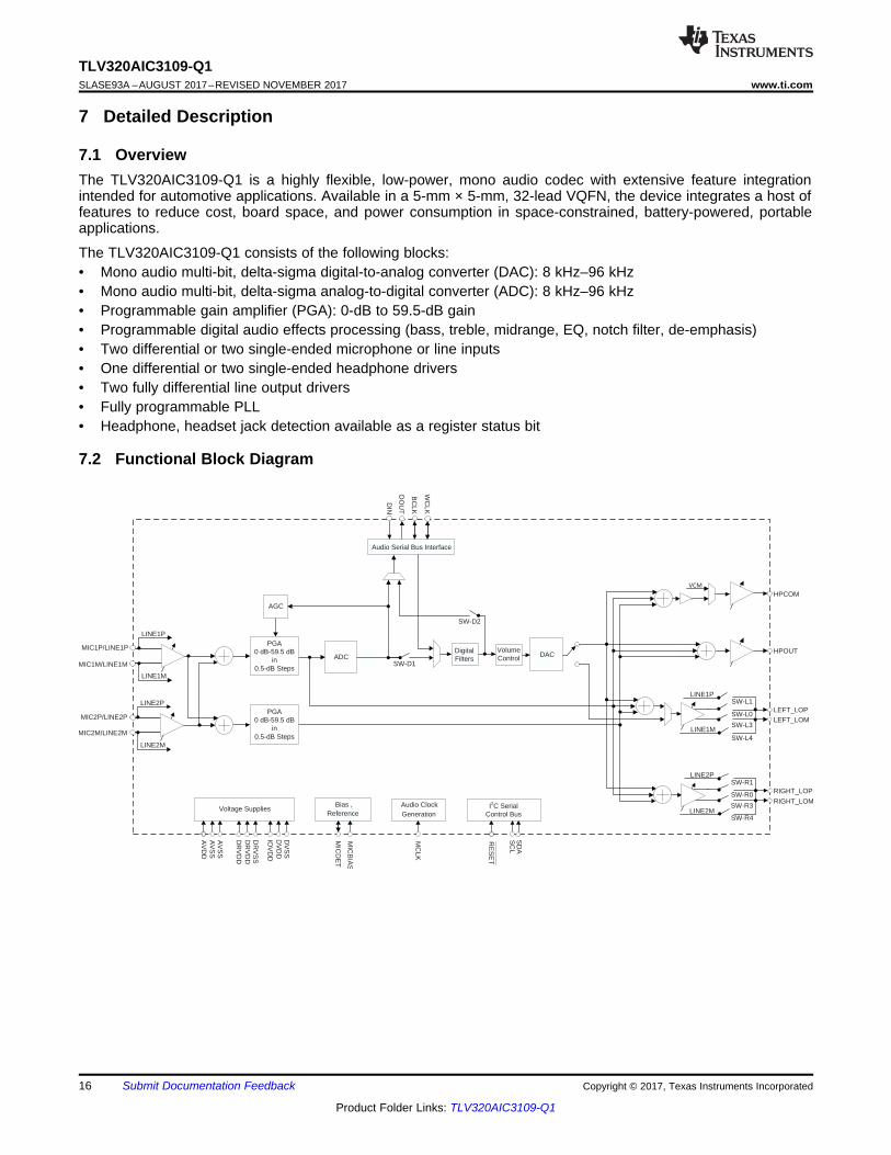
7 Detailed Description
7.1 OverviewThe TLV320AIC3109-Q1 is a highly flexible, low-power, mono audio codec with extensive feature integrationintended for automotive applications. Available in a 5-mm × 5-mm, 32-lead VQFN, the device integrates a host offeatures to reduce cost, board space, and power consumption in space-constrained, battery-powered, portableapplications.
The TLV320AIC3109-Q1 consists of the following blocks:• Mono audio multi-bit, delta-sigma digital-to-analog converter (DAC): 8 kHz–96 kHz• Mono audio multi-bit, delta-sigma analog-to-digital converter (ADC): 8 kHz–96 kHz• Programmable gain amplifier (PGA): 0-dB to 59.5-dB gain• Programmable digital audio effects processing (bass, treble, midrange, EQ, notch filter, de-emphasis)• Two differential or two single-ended microphone or line inputs• One differential or two single-ended headphone drivers• Two fully differential line output drivers• Fully programmable PLL• Headphone, headset jack detection available as a register status bit
7.2 Functional Block Diagram
17
TLV320AIC3109-Q1www.ti.com SLASE93A –AUGUST 2017–REVISED NOVEMBER 2017
Product Folder Links: TLV320AIC3109-Q1
Submit Documentation FeedbackCopyright © 2017, Texas Instruments Incorporated
7.3 Feature Description
7.3.1 Hardware ResetThe TLV320AIC3109-Q1 requires a hardware reset after power-up for proper operation. After all power suppliesare at their specified values, the RESET pin must be driven low for at least 10 ns. If this reset sequence is notperformed, the TLV320AIC3109-Q1 may not respond properly to register reads or writes.
This device also offers a software reset (page 0, register 1) that can be used by the host to reset all registers onpage 0 and page 1 to their reset values. In cases where changes are needed only for routing or volume-controlregisters, these changes can be accomplished by writing directly to the appropriate registers rather than usingthe software or hardware reset.
In cases where the ESD events generate a device reset, a minimum 1-nF capacitor is recommended to beconnected between the RESET pin and DVSS. This capacitor avoids ESD events that can place the codec indefault state.
7.3.2 Digital Audio Data Serial InterfaceAudio data are transferred between the host processor and the TLV320AIC3109-Q1 via the digital audio dataserial interface. The audio bus of the TLV320AIC3109-Q1 can be configured for left- or right-justified, I2S, DSP,or TDM modes of operation, where communication with standard PCM interfaces is supported within TDM mode.These modes are all MSB-first, with data width programmable as 16, 20, 24, or 32 bits. In addition, the wordclock (WCLK) and bit clock (BCLK) can be independently configured in either master or slave mode for flexibleconnectivity to a wide variety of processors.
The word clock (WCLK) is used to define the beginning of a frame, and can be programmed as either a pulse ora square-wave signal. The frequency of this clock corresponds to the selected ADC and DAC samplingfrequency.
The bit clock (BCLK) is used to clock in and out the digital audio data across the serial bus. When in mastermode, this signal can be programmed in two further modes: continuous transfer mode, and 256-clock mode. Incontinuous transfer mode, only the minimal number of bit clocks required to transfer the audio data aregenerated, so in general the number of bit clocks per frame is two times the data width. For example, if the datawidth is chosen as 16 bits, then 32-bit clocks are generated per frame. If the bit clock signal in master mode is tobe used by a PLL in another device, then the 16-bit or 32-bit data-width selections are recommended be used.These cases result in a low-jitter bit clock signal being generated, with frequencies of 32 fS or 64 fS. For a 20-bitand 24-bit data width in master mode, the bit clocks generated in each frame are not all of equal period becausethe device does not have a clean 40-fS or 48-fS clock signal readily available. The average frequency of the bitclock signal is still accurate in these cases (40 fS or 48 fS), but the resulting clock signal has higher jitter than inthe 16-bit and 32-bit cases.
In 256-clock mode, a constant 256 bit clocks per frame are generated, independent of the data width chosen.The TLV320AIC3109-Q1 further includes programmability to place the DOUT line in the high-impedance stateduring all bit clocks when valid data are not being sent. By combining this capability with the ability to program atwhat bit clock in a frame the audio data begins, time-division multiplexing (TDM) can be accomplished, resultingin multiple codecs able to use a single audio serial data bus.
When the digital audio data serial interface is powered down when configured in master mode, the pinsassociated with the interface are put into a high-impedance state.
The following subsections describe the supported data interface protocols. These protocols can be used for left-and right-channel applications. Only one of the two possible channels can be selected because theTLV320AIC3109-Q1 is a mono audio codec. Only the left channel is valid for DOUT (output data). For DIN (inputdata), valid data can be selected with bits 4 and 3 of register 7, page 0.
BCLK
WCLK
1 10 00
T0150-01
1/fs
LSBMSB
Left Channel Right Channel
2 2SDIN/SDOUT n–1 n–1 n–1n–2 n–2 n–2n–3 n–3
BCLK
WCLK
1 00 1 0
T0149-01
1/fs
LSBMSB
Left Channel Right Channel
2 2SDIN/SDOUT n–1 n–1n–2 n–2n–3 n–3
18
TLV320AIC3109-Q1SLASE93A –AUGUST 2017–REVISED NOVEMBER 2017 www.ti.com
Product Folder Links: TLV320AIC3109-Q1
Submit Documentation Feedback Copyright © 2017, Texas Instruments Incorporated
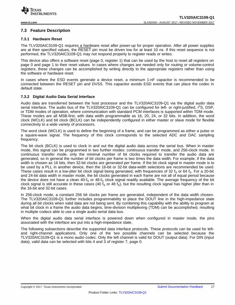
Feature Description (continued)7.3.2.1 Right-Justified ModeIn right-justified mode, the LSB of the left channel is valid on the rising edge of the bit clock preceding the fallingedge of the word clock. Similarly, the LSB of the right channel is valid on the rising edge of the bit clockpreceding the rising edge of the word clock. Figure 12 shows a timing diagram of this operation.
Figure 12. Right-Justified Serial Data Bus Mode Operation
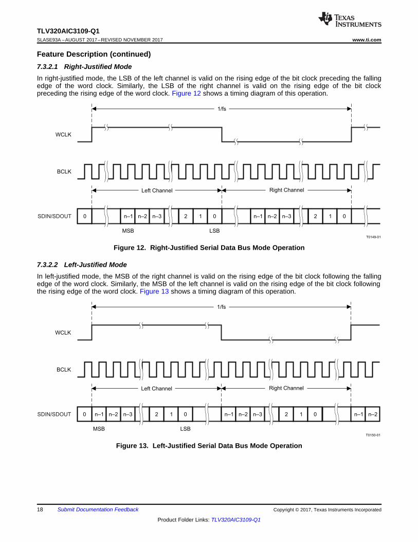
7.3.2.2 Left-Justified ModeIn left-justified mode, the MSB of the right channel is valid on the rising edge of the bit clock following the fallingedge of the word clock. Similarly, the MSB of the left channel is valid on the rising edge of the bit clock followingthe rising edge of the word clock. Figure 13 shows a timing diagram of this operation.
Figure 13. Left-Justified Serial Data Bus Mode Operation
BCLK
WCLK
0 0
T0152-01
1/fs
LSB LSBLSB MSB MSB
Left Channel Right Channel
1 12 2SDIN/SDOUT n–1 n–1n–1n–2 n–3 n–3n–4 n–2
BCLK
WCLK
1 10 0
T0151-01
1/fs
LSBMSB
Left Channel Right Channel
2 2SDIN/SDOUT n–1 n–1 n–1
1 Clock Before MSB
n–2 n–2n–3 n–3
19
TLV320AIC3109-Q1www.ti.com SLASE93A –AUGUST 2017–REVISED NOVEMBER 2017
Product Folder Links: TLV320AIC3109-Q1
Submit Documentation FeedbackCopyright © 2017, Texas Instruments Incorporated
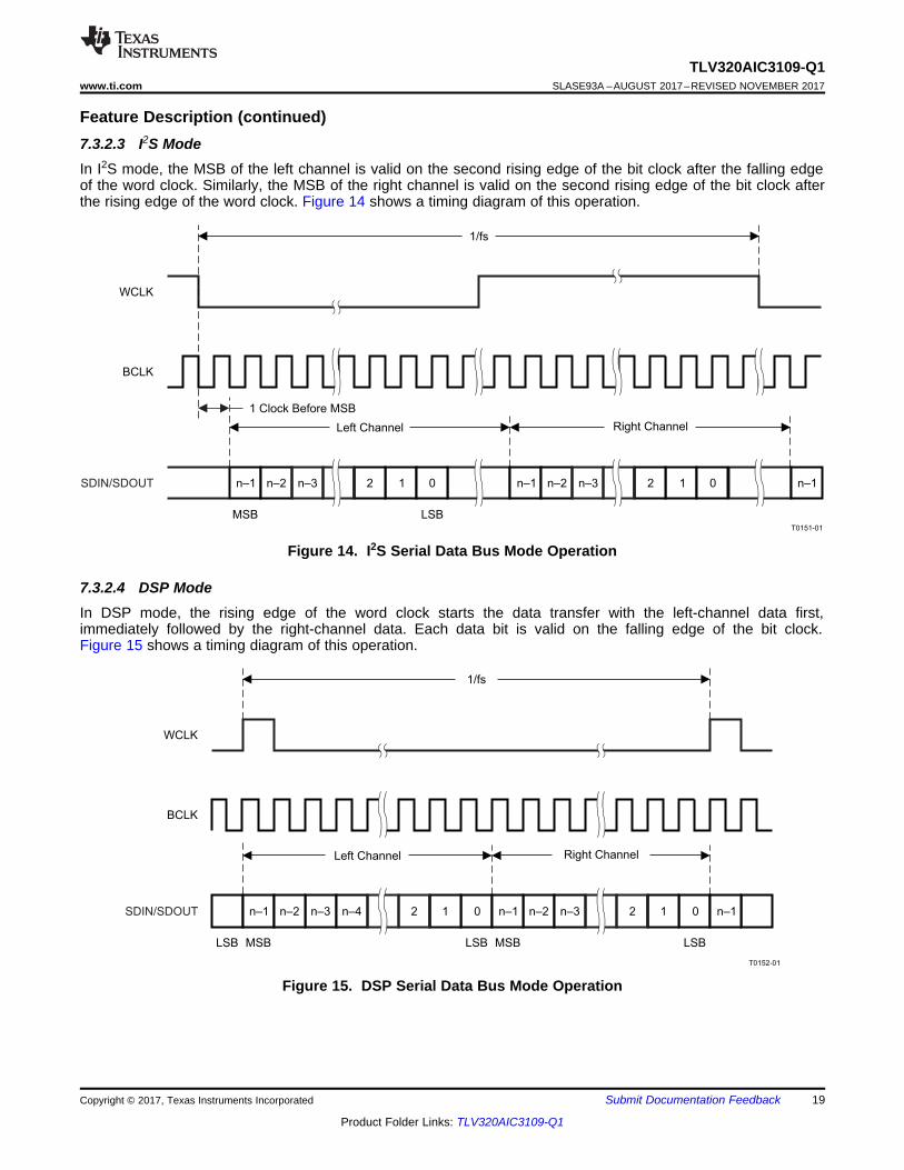
Feature Description (continued)7.3.2.3 I2S ModeIn I2S mode, the MSB of the left channel is valid on the second rising edge of the bit clock after the falling edgeof the word clock. Similarly, the MSB of the right channel is valid on the second rising edge of the bit clock afterthe rising edge of the word clock. Figure 14 shows a timing diagram of this operation.
Figure 14. I2S Serial Data Bus Mode Operation
7.3.2.4 DSP ModeIn DSP mode, the rising edge of the word clock starts the data transfer with the left-channel data first,immediately followed by the right-channel data. Each data bit is valid on the falling edge of the bit clock.Figure 15 shows a timing diagram of this operation.
Figure 15. DSP Serial Data Bus Mode Operation
N–1
N–1 N–1
1
1 1
1N–1N–2
N–2 N–2
0
0 0
0N–2
Right-Channel Data
Right-Channel Data
Left-Channel Data
Left-Channel Data
• • • •
• • • • • • • •
• • • • • •
DSP Mode
Left-Justified Mode
Offset
Offset Offset
T0153-01
Word Clock
Word Clock
Bit Clock
Bit Clock
Data In/Out
Data In/Out
20
TLV320AIC3109-Q1SLASE93A –AUGUST 2017–REVISED NOVEMBER 2017 www.ti.com
Product Folder Links: TLV320AIC3109-Q1
Submit Documentation Feedback Copyright © 2017, Texas Instruments Incorporated
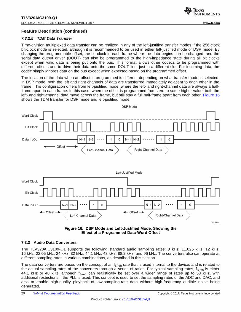
Feature Description (continued)7.3.2.5 TDM Data TransferTime-division multiplexed data transfer can be realized in any of the left-justified transfer modes if the 256-clockbit-clock mode is selected, although it is recommended to be used in either left-justified mode or DSP mode. Bychanging the programmable offset, the bit clock in each frame where the data begins can be changed, and theserial data output driver (DOUT) can also be programmed to the high-impedance state during all bit clocksexcept when valid data is being put onto the bus. This format allows other codecs to be programmed withdifferent offsets and to drive their data onto the same DOUT line, just in a different slot. For incoming data, thecodec simply ignores data on the bus except when expected based on the programmed offset.
The location of the data when an offset is programmed is different depending on what transfer mode is selected.In DSP mode, both the left and right channels of data are transferred immediately adjacent to each other in theframe. This configuration differs from left-justified mode, where the left- and right-channel data are always a half-frame apart in each frame. In this case, when the offset is programmed from zero to some higher value, both theleft- and right-channel data move across the frame, but still stay a full half-frame apart from each other. Figure 16shows the TDM transfer for DSP mode and left-justified mode.
Figure 16. DSP Mode and Left-Justified Mode, Showing theEffect of a Programmed Data-Word Offset
7.3.3 Audio Data ConvertersThe TLV320AIC3109-Q1 supports the following standard audio sampling rates: 8 kHz, 11.025 kHz, 12 kHz,16 kHz, 22.05 kHz, 24 kHz, 32 kHz, 44.1 kHz, 48 kHz, 88.2 kHz, and 96 kHz. The converters also can operate atdifferent sampling rates in various combinations, as described in this section.
The data converters are based on the concept of an fS(ref) rate that is used internal to the device, and is related tothe actual sampling rates of the converters through a series of ratios. For typical sampling rates, fS(ref) is either44.1 kHz or 48 kHz, although fS(ref) can realistically be set over a wider range of rates up to 53 kHz, withadditional restrictions if the PLL is used. This concept is used to set the sampling rates of the ADC and DAC, andalso to enable high-quality playback of low-sampling-rate data without high-frequency audible noise beinggenerated.
K*R/P2/Q
PLL_CLKIN
CODEC
CODEC_CLKIN
PLL_OUT
Q = 2, 3,….., 16, 17
MCLK BCLK
CLKDIV_IN PLL_IN
B0153-01
DAC fS ADC fS
CODEC_CLK = 256 f´ S(ref)
CLKDIV_OUT
1/8
PLLDIV_OUT
CLKDIV_CLKIN
K = J.DJ = 1, 2, 3, ...., 62, 63D = 0000, 0001, ...., 9998, 9999R = 1, 2, 3, 4, ...., 15, 16P = 1, 2, ...., 7, 8
WCLK = /NCODEC
CODEC = DAC = ADC
Set NCODEC = NADC = NDAC = 1, 1.5, 2, ...., 5.5, 6DAC DRA => NDAC = 0.5ADC DRA => NADC = 0.5
f
f f f
S(ref)
S S S
21
TLV320AIC3109-Q1www.ti.com SLASE93A –AUGUST 2017–REVISED NOVEMBER 2017
Product Folder Links: TLV320AIC3109-Q1
Submit Documentation FeedbackCopyright © 2017, Texas Instruments Incorporated
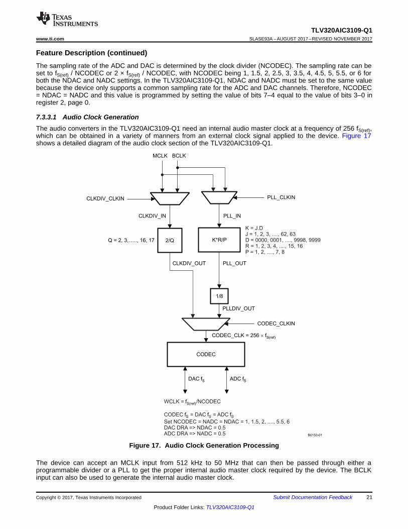
Feature Description (continued)The sampling rate of the ADC and DAC is determined by the clock divider (NCODEC). The sampling rate can beset to fS(ref) / NCODEC or 2 × fS(ref) / NCODEC, with NCODEC being 1, 1.5, 2, 2.5, 3, 3.5, 4, 4.5, 5, 5.5, or 6 forboth the NDAC and NADC settings. In the TLV320AIC3109-Q1, NDAC and NADC must be set to the same valuebecause the device only supports a common sampling rate for the ADC and DAC channels. Therefore, NCODEC= NDAC = NADC and this value is programmed by setting the value of bits 7–4 equal to the value of bits 3–0 inregister 2, page 0.
7.3.3.1 Audio Clock GenerationThe audio converters in the TLV320AIC3109-Q1 need an internal audio master clock at a frequency of 256 fS(ref),which can be obtained in a variety of manners from an external clock signal applied to the device. Figure 17shows a detailed diagram of the audio clock section of the TLV320AIC3109-Q1.
Figure 17. Audio Clock Generation Processing
The device can accept an MCLK input from 512 kHz to 50 MHz that can then be passed through either aprogrammable divider or a PLL to get the proper internal audio master clock required by the device. The BCLKinput can also be used to generate the internal audio master clock.

22
TLV320AIC3109-Q1SLASE93A –AUGUST 2017–REVISED NOVEMBER 2017 www.ti.com
Product Folder Links: TLV320AIC3109-Q1
Submit Documentation Feedback Copyright © 2017, Texas Instruments Incorporated
Feature Description (continued)A primary concern is proper operation of the codec at various sample rates with the limited MCLK frequenciesavailable in the system. This device includes a highly programmable PLL to accommodate such situations easily.The integrated PLL can generate audio clocks from a wide variety of possible MCLK inputs, with particular focuspaid to the standard MCLK rates already widely used.
When the PLL is disabled,fS(ref) = CLKDIV_IN / (128 × Q)
where• Q = 2, 3…17; Q is register-programmable and can be set by bits 6–3 in register 3, page 0 (1)
CLKDIV_IN can be MCLK or BCLK, selected by register 102, bits 7–6.
NOTEWhen NCODEC = 1.5, 2.5, 3.5, 4.5, or 5.5, odd values of Q are not allowed. In this mode,MCLK can be as high as 50 MHz, and fS(ref) must fall within 39 kHz to 53 kHz, inclusively.
When the PLL is enabled,fS(ref) = (PLLCLK_IN × K × R) / (2048 × P)
where• P = 1, 2, 3…8• R = 1, 2…16• K = J.D• J = 1, 2, 3…63• D = 0000, 0001, 0002, 0003…9998, 9999• PLLCLK_IN can be MCLK or BCLK, selected by bits 5–4 in register 102, page 0 (2)
P, R, J, and D are register programmable. J is the integer portion of K (the numbers to the left of the decimalpoint), whereas D is the fractional portion of K (the numbers to the right of the decimal point, assuming four digitsof precision). P can be set by bits 2–0 in register 3, page 0. R can be set by bits 3–0 in register 11, page 0. J canbe set by bits 7–2 in register 4, page 0. The most-significant bits of D can be set by bits 7–0 in register 5, page 0,and the least-significant bits of D can be set by bits 7–2 in register 6, page 0.
Examples:If K = 8.5, then J = 8, D = 5000If K = 7.12, then J = 7, D = 1200If K = 14.03, then J = 14, D = 0300If K = 6.0004, then J = 6, D = 0004
When the PLL is enabled and D = 0000, the following conditions must be satisfied to meet specifiedperformance:
2 MHz ≤ (PLLCLK_IN / P) ≤ 20 MHz80 MHz ≤ (PLLCLK _IN × K × R / P) ≤ 110 MHz4 ≤ J ≤ 55
When the PLL is enabled and D ≠ 0000, the following conditions must be satisfied to meet specifiedperformance:
10 MHz ≤ PLLCLK _IN / P ≤ 20 MHz80 MHz ≤ PLLCLK _IN × K × R / P ≤ 110 MHz4 ≤ J ≤ 11R = 1
Example:MCLK = 12 MHz and fS(ref) = 44.1 kHzSelect P = 1, R = 1, K = 7.5264, which results in J = 7, D = 5264
23
TLV320AIC3109-Q1www.ti.com SLASE93A –AUGUST 2017–REVISED NOVEMBER 2017
Product Folder Links: TLV320AIC3109-Q1
Submit Documentation FeedbackCopyright © 2017, Texas Instruments Incorporated
Feature Description (continued)Example:
MCLK = 12 MHz and fS(ref) = 48 kHzSelect P = 1, R = 1, K = 8.192, which results in J = 8, D = 1920
Table 1 lists several example cases of typical MCLK rates and how to program the PLL to achieve fS(ref) =44.1 kHz or 48 kHz.
Table 1. Typical MCLK RatesMCLK (MHz) P R J D ACHIEVED fS(ref) % ERRORfS(ref) = 44.1 kHz2.8224 1 1 32 0 44,100 05.6448 1 1 16 0 44,100 012 1 1 7 5264 44,100 013 1 1 6 9474 44,099.71 –0.000716 1 1 5 6448 44,100 019.2 1 1 4 7040 44,100 019.68 1 1 4 5893 44,100.3 0.000748 4 1 7 5264 44,100 0fS(ref) = 48 kHz2.048 1 1 48 0 48,000 03.072 1 1 32 0 48,000 04.096 1 1 24 0 48,000 06.144 1 1 16 0 48,000 08.192 1 1 12 0 48,000 012 1 1 8 1920 48,000 013 1 1 7 5618 47,999.71 –0.000616 1 1 6 1440 48,000 019.2 1 1 5 1200 48,000 019.68 1 1 4 9951 47,999.79 –0.000448 4 1 8 1920 48,000 0
7.3.3.2 Mono Audio ADCThe TLV320AIC3109-Q1 includes a mono audio ADC that uses a delta-sigma modulator with 128-timesoversampling in single-rate mode, followed by a digital decimation filter. The ADC supports sampling rates from8 kHz to 96 kHz. Whenever the ADC or DAC is in operation, the device requires that an audio master clock beprovided and appropriate audio clock generation be set up within the device.
The integrated digital decimation filter removes high-frequency content and downsamples the audio data from aninitial sampling rate of 128 fS to the final output sampling rate of fS. The decimation filter provides a linear phaseoutput response with a group delay of 17 / fS. The –3-dB bandwidth of the decimation filter extends to 0.45 fS andscales with the sample rate (fS). The filter has minimum 75-dB attenuation over the stop band from 0.55 fS to 64fS. The device also provide options to select the corner frequency of the digital high-pass filter.
Requirements for analog antialiasing filtering are very relaxed because of the oversampling nature of the audioADC and the integrated digital decimation filtering. The TLV320AIC3109-Q1 integrates a second-order analogantialiasing filter with 20-dB attenuation at 1 MHz. This filter, combined with the digital decimation filter, providessufficient antialiasing filtering without requiring additional external components.
The ADC is preceded by a programmable gain amplifier (PGA) that allows analog gain control from 0 dB to59.5 dB in steps of 0.5 dB. The PGA gain changes are implemented with an internal soft-stepping algorithm thatonly changes the actual volume level by one 0.5-dB step every one or two ADC output samples, depending onthe register programming (see registers 19 and 22, page 0). This soft-stepping ensures that volume controlchanges occur smoothly with no audible artifacts. On reset, the PGA gain defaults to a mute condition, and on
H(z) N0 N1 z1
32, 768 D1 z1
24
TLV320AIC3109-Q1SLASE93A –AUGUST 2017–REVISED NOVEMBER 2017 www.ti.com
Product Folder Links: TLV320AIC3109-Q1
Submit Documentation Feedback Copyright © 2017, Texas Instruments Incorporated
power-down, the PGA soft-steps the volume to mute before shutting down. A read-only flag is set whenever thegain applied by PGA equals the desired value set by the register. The soft-stepping control can also be disabledby programming a register bit. When soft-stepping is enabled, the audio master clock must be applied to thedevice after the ADC power-down register is written to ensure the soft-stepping to mute has completed. Whenthe ADC power-down flag is no longer set, the audio master clock can be shut down.
An additional auxiliary PGA is provided to allow the mixing of the DAC output signals with an input not routedthrough the ADC. This PGA has the same specifications as the ADC PGA.
7.3.3.2.1 Mono Audio ADC High-Pass Filter
Often in audio applications, the dc offset needs to be removed from the converted audio data stream. TheTLV320AIC3109-Q1 has a programmable first-order, high-pass filter that can be used for this purpose. Thedigital filter coefficients are in 16-bit format and therefore use two 8-bit registers for each of the three coefficients,N0, N1, and D1. Equation 3 shows the form of the digital high-pass filter transfer function:
(3)
Programming the channel is done by writing to registers 65–70, page 1. After the coefficients are loaded, theseADC high-pass filter coefficients can be selected by writing to bit 7 in register 107, page 0, and the high-passfilter can be enabled by writing to bit 7 in register 12, page 0.
7.3.3.2.2 Automatic Gain Control (AGC)
An automatic gain control (AGC) circuit is included with the ADC and can be used to maintain nominally constantoutput signal amplitude when recording speech signals (the AGC can be fully disabled if not needed). Thiscircuitry automatically adjusts the PGA gain when the input signal becomes overly loud or very weak, such aswhen a person speaking into a microphone moves closer or farther from the microphone. The AGC algorithm hasseveral programmable settings, including target level, attack and decay time constants, noise threshold, andmaximum PGA gain applicable that allow the algorithm to be fine-tuned for any particular application. These AGCfeatures are explained in this section, and Figure 18 illustrates their operation. The algorithm uses the absoluteaverage of the signal (which is the average of the absolute value of the signal) as a measure of the nominalamplitude of the output signal.

W0002-01
Decay Time
TargetLevel
InputSignal
OutputSignal
AGCGain
AttackTime
25
TLV320AIC3109-Q1www.ti.com SLASE93A –AUGUST 2017–REVISED NOVEMBER 2017
Product Folder Links: TLV320AIC3109-Q1
Submit Documentation FeedbackCopyright © 2017, Texas Instruments Incorporated
Figure 18. Typical Operation of the AGC Algorithm During Speech Recording
7.3.3.2.2.1 Target Level
Target value represents the nominal output level at which the AGC attempts to hold the ADC output signal level.The TLV320AIC3109-Q1 allows programming of eight different target levels, which can be programmed from–5.5 dB to –24 dB relative to a full-scale signal. The target level is recommended to be set with enough margin toavoid clipping at the occurrence of loud sounds because the device reacts to the signal absolute average and notto peak levels.
7.3.3.2.2.2 Attack Time
Attack time determines how quickly the AGC circuitry reduces the PGA gain when the input signal is too loud. ItAttack time can be varied from 7 ms to 1,408 ms. The attack time can be programmed by writing to register 105,page 0.
7.3.3.2.2.3 Decay Time
Decay time determines how quickly the PGA gain is increased when the input signal is too low. It Decay time canbe varied in the range from 0.05 s to 22.4 s. Decay time is programmed by writing to register 106, page 0.
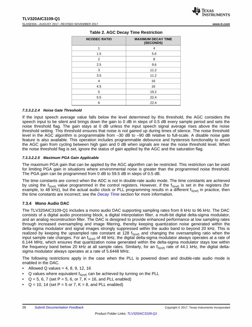
The actual maximum AGC decay time is based on a counter length, so the maximum decay time scales with theclock setup that is used. Table 2 lists the relationship of the NCODEC ratio to the maximum time available for theAGC decay. In practice, these maximum times are extremely long for audio applications and must not limit anypractical AGC decay time that is needed by the system.
26
TLV320AIC3109-Q1SLASE93A –AUGUST 2017–REVISED NOVEMBER 2017 www.ti.com
Product Folder Links: TLV320AIC3109-Q1
Submit Documentation Feedback Copyright © 2017, Texas Instruments Incorporated
Table 2. AGC Decay Time RestrictionNCODEC RATIO MAXIMUM DECAY TIME
(SECONDS)1 4
1.5 5.62 8
2.5 9.63 11.2
3.5 11.24 16
4.5 165 19.2
5.5 22.46 22.4
7.3.3.2.2.4 Noise Gate Threshold
If the input speech average value falls below the level determined by this threshold, the AGC considers thespeech input to be silent and brings down the gain to 0 dB in steps of 0.5 dB every sample period and sets thenoise threshold flag. The gain stays at 0 dB unless the input speech signal average rises above the noisethreshold setting. This threshold ensures that noise is not gained up during times of silence. The noise thresholdlevel in the AGC algorithm is programmable from –30 dB to –90 dB relative to full-scale. A disable noise gatefeature is also available. This operation includes programmable debounce and hysteresis functionality to avoidthe AGC gain from cycling between high gain and 0 dB when signals are near the noise threshold level. Whenthe noise threshold flag is set, ignore the status of gain applied by the AGC and the saturation flag.
7.3.3.2.2.5 Maximum PGA Gain Applicable
The maximum PGA gain that can be applied by the AGC algorithm can be restricted. This restriction can be usedfor limiting PGA gain in situations where environmental noise is greater than the programmed noise threshold.The PGA gain can be programmed from 0 dB to 59.5 dB in steps of 0.5 dB.
The time constants are correct when the ADC is not in double-rate audio mode. The time constants are achievedby using the fS(ref) value programmed in the control registers. However, if the fS(ref) is set in the registers (forexample, to 48 kHz), but the actual audio clock or PLL programming results in a different fS(ref) in practice, thenthe time constants are incorrect; see the Decay Time section for more information.
7.3.4 Mono Audio DACThe TLV320AIC3109-Q1 includes a mono audio DAC supporting sampling rates from 8 kHz to 96 kHz. The DACconsists of a digital audio processing block, a digital interpolation filter, a multi-bit digital delta-sigma modulator,and an analog reconstruction filter. The DAC is designed to provide enhanced performance at low sampling ratesthrough increased oversampling and image filtering, thereby keeping quantization noise generated within thedelta-sigma modulator and signal images strongly suppressed within the audio band to beyond 20 kHz. This isrealized by keeping the upsampled rate constant at 128 fS(ref) and changing the oversampling ratio when theinput sample rate changes. For an fS(ref) of 48 kHz, the digital delta-sigma modulator always operates at a rate of6.144 MHz, which ensures that quantization noise generated within the delta-sigma modulator stays low withinthe frequency band below 20 kHz at all sample rates. Similarly, for an fS(ref) rate of 44.1 kHz, the digital delta-sigma modulator always operates at a rate of 5.6448 MHz.
The following restrictions apply in the case when the PLL is powered down and double-rate audio mode isenabled in the DAC.• Allowed Q values = 4, 8, 9, 12, 16• Q values where equivalent fS(ref) can be achieved by turning on the PLL• Q = 5, 6, 7 (set P = 5, 6, or 7, K = 16, and PLL enabled)• Q = 10, 14 (set P = 5 or 7, K = 8, and PLL enabled)

LB1 LB2
B0154-01
N0 2 N1 z1 N2 z2
32, 768 2 D1 z1 D2 z2 N3 2 N4 z1 N5 z2
32, 768 2 D4 z1 D5 z2
H(z) N0 N1 z1
32, 768 D1 z1
27
TLV320AIC3109-Q1www.ti.com SLASE93A –AUGUST 2017–REVISED NOVEMBER 2017
Product Folder Links: TLV320AIC3109-Q1
Submit Documentation FeedbackCopyright © 2017, Texas Instruments Incorporated
7.3.4.1 Digital Audio Processing for PlaybackThe DAC channel consists of optional filters for de-emphasis and bass, treble, midrange level adjustment, andspeaker equalization. The de-emphasis function is implemented by a programmable digital filter block with fullyprogrammable coefficients (see registers 21–26, page 1). If de-emphasis is not required in a particularapplication, this programmable filter block can be used for some other purpose. Equation 4 gives the de-emphasis filter transfer function:
where• The N0, N1, and D1 coefficients are fully programmable individually (4)
Table 3 lists the coefficients that must be loaded to implement standard de-emphasis filters.
(1) The 48-kHz coefficients listed in Table 3 are used as defaults.
Table 3. De-Emphasis Coefficients for Common Audio Sampling RatesSAMPLING FREQUENCY N0 N1 D1
32 kHz 16,950 –1,220 17,03744.1 kHz 15,091 –2,877 20,55548 kHz (1) 14,677 –3,283 21,374
In addition to the de-emphasis filter block, the DAC digital effects processing includes a fourth-order digital IIRfilter with programmable coefficients. This filter is implemented as a cascade of two biquad sections with thefrequency response given by:
(5)
The N and D coefficients are fully programmable and the entire filter can be enabled or bypassed. The structureof the filtering when configured for channel processing is illustrated in Figure 19, with LB1 corresponding to thefirst biquad filter using coefficients N0, N1, N2, D1, and D2. LB2 similarly corresponds to the second biquad filterusing coefficients N3, N4, N5, D4, and D5.
Figure 19. Structure of Digital Effects Processing for Channel Processing
The coefficients for this filter implement a variety of sound effects, with bass boost or treble boost being the mostcommonly used in portable audio applications. The default N and D coefficients in the device are given in Table 4and implement a shelving filter with 0-dB gain from dc to approximately 150 Hz, at which point the filter rolls off toa 3-dB attenuation for higher frequency signals, thus giving a 3-dB boost to signals below 150 Hz. The N and Dcoefficients are represented by 16-bit, 2's-complement numbers with values ranging from –32,768 to 32,767.
Table 4. Default Digital Effects Processing Filter Coefficients,When in Independent Channel Processing Configuration
COEFFICIENTSN0 = N3 D1 = D4 N1 = N4 D2 = D5 N2 = N527,619 32,131 –27,034 –31,506 26,461
28
TLV320AIC3109-Q1SLASE93A –AUGUST 2017–REVISED NOVEMBER 2017 www.ti.com
Product Folder Links: TLV320AIC3109-Q1
Submit Documentation Feedback Copyright © 2017, Texas Instruments Incorporated
The digital effects filters are recommended to be disabled when the filter coefficients are being modified. Whennew coefficients are being written to the device over the control port, a filter using partially updated coefficientscan possibly implement an unstable system and lead to oscillation or objectionable audio output. By disabling thefilters, changing the coefficients, and then reenabling the filters, these types of effects can be entirely avoided.
7.3.4.2 Digital Interpolation FilterThe digital interpolation filter upsamples the output of the digital audio processing block by the requiredoversampling ratio before data are provided to the digital delta-sigma modulator and analog reconstruction filterstages. The filter provides a linear phase output with a group delay of 21 / fS. In addition, programmable digitalinterpolation filtering is included to provide enhanced image filtering and reduce signal images caused by theupsampling process that are below 20 kHz. For example, upsampling an 8-kHz signal produces signal images atmultiples of 8-kHz (that is, 8 kHz, 16 kHz, 24 kHz, and so forth). The images at 8 kHz and 16 kHz are below20 kHz and are still audible to the listener; therefore, these images must be filtered heavily to maintain a goodquality output. The interpolation filter is designed to maintain at least 65-dB rejection of images that are below7.455 fS. In order to use the programmable interpolation capability, program fS(ref) to a higher rate (restricted to bein the range of 39 kHz to 53 kHz when the PLL is in use), and the actual fS is set using the NCODEC divider,where NCODEC = NDAC = NADC. For example, if fS = 8 kHz is required, then fS(ref) can be set to 48 kHz andthe DAC fS set to fS(ref) / 6. This setting ensures that all images of the 8-kHz data are sufficiently attenuated wellbeyond a 20-kHz audible frequency range.
7.3.4.3 Delta-Sigma Audio DACThe mono audio DAC incorporates a third-order, multi-bit, delta-sigma modulator followed by an analogreconstruction filter. The DAC provides high-resolution, low-noise performance, using oversampling and noiseshaping techniques. The analog reconstruction filter design consists of a six-tap analog FIR filter followed by acontinuous-time RC filter. The analog FIR operates at a rate of 128 fS(ref) (6.144 MHz when fS(ref) = 48 kHz,5.6448 MHz when fS(ref) = 44.1 kHz). The DAC analog performance can be degraded by excessive clock jitter onthe MCLK input. Therefore, care must be taken to keep jitter on this clock to a minimum.
7.3.4.4 Audio DAC Digital Volume ControlThe audio DAC includes a digital volume control block that implements a programmable digital gain. The volumelevel can be varied from 0 dB to –63.5 dB in 0.5-dB steps, or set to mute, independently for each channel. Thevolume level can also be changed by the master volume control. Gain changes are implemented with a soft-stepping algorithm that only changes the actual volume by one step per input sample, either up or down, until thedesired volume is reached. The rate of soft-stepping can be slowed to one step per two input samples through aregister bit.
The host does not know when the DAC is muted because of the soft-stepping, which may be important if thehost wishes to mute the DAC before making a significant change, such as changing sample rates. In order tohelp with this situation, the device provides a flag back to the host via a read-only register bit that alerts the hostwhen the device completes the soft-stepping and the actual volume reaches the desired volume level. The soft-stepping feature can be disabled through register programming. If soft-stepping is enabled, keep the MCLKsignal applied to the device until the DAC power-down flag is set. When this flag is set, the internal soft-steppingprocess and power-down sequence is complete, and the MCLK can then be stopped if desired.
The TLV320AIC3109-Q1 also includes functionality to detect when the selection of de-emphasis or digital audioprocessing functionality is changed. When the new selection is detected, the TLV320AIC3109-Q1 (1) soft-mutesthe DAC volume control, (2) changes the operation of the digital effects processing to match the new selection,and (3) soft-unmutes the device. These steps avoid any possible pops or clicks in the audio output resulting frominstantaneous changes in the filtering. A similar algorithm is used when first powering up or powering down theDAC. The circuit begins operation at power-up with the volume control muted, then soft-steps the volume up tothe desired level. At power-down, the logic first soft-steps the volume down to a mute level, then powers downthe circuitry.
7.3.4.5 Increasing DAC Dynamic RangeThe TLV320AIC3109-Q1 allows trading off dynamic range with power consumption. The DAC dynamic range canbe increased by writing to bits 7–6 in register 109, page 0. The lowest DAC current setting is the default, and thedynamic range is displayed in the Audio DAC, Differential Line Output section of the Electrical Characteristicstable. Increasing the current can increase the DAC dynamic range by up to 1.5 dB.
29
TLV320AIC3109-Q1www.ti.com SLASE93A –AUGUST 2017–REVISED NOVEMBER 2017
Product Folder Links: TLV320AIC3109-Q1
Submit Documentation FeedbackCopyright © 2017, Texas Instruments Incorporated
7.3.4.6 Analog Output Common-mode AdjustmentThe output common-mode voltage and output range of the analog output are determined by an internal band-gapreference, in contrast to other codecs that can use a scaled version of the analog supply. This scheme is used toreduce noise coupling that can be on the supply (such as 217-Hz noise in a GSM cell phone) into the audiosignal path.
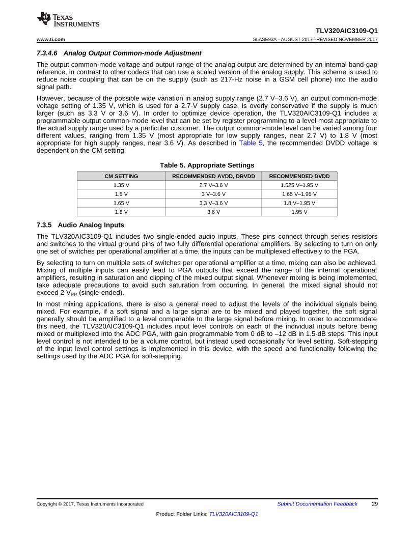
However, because of the possible wide variation in analog supply range (2.7 V–3.6 V), an output common-modevoltage setting of 1.35 V, which is used for a 2.7-V supply case, is overly conservative if the supply is muchlarger (such as 3.3 V or 3.6 V). In order to optimize device operation, the TLV320AIC3109-Q1 includes aprogrammable output common-mode level that can be set by register programming to a level most appropriate tothe actual supply range used by a particular customer. The output common-mode level can be varied among fourdifferent values, ranging from 1.35 V (most appropriate for low supply ranges, near 2.7 V) to 1.8 V (mostappropriate for high supply ranges, near 3.6 V). As described in Table 5, the recommended DVDD voltage isdependent on the CM setting.
Table 5. Appropriate SettingsCM SETTING RECOMMENDED AVDD, DRVDD RECOMMENDED DVDD
1.35 V 2.7 V–3.6 V 1.525 V–1.95 V1.5 V 3 V–3.6 V 1.65 V–1.95 V1.65 V 3.3 V–3.6 V 1.8 V–1.95 V1.8 V 3.6 V 1.95 V
7.3.5 Audio Analog InputsThe TLV320AIC3109-Q1 includes two single-ended audio inputs. These pins connect through series resistorsand switches to the virtual ground pins of two fully differential operational amplifiers. By selecting to turn on onlyone set of switches per operational amplifier at a time, the inputs can be multiplexed effectively to the PGA.
By selecting to turn on multiple sets of switches per operational amplifier at a time, mixing can also be achieved.Mixing of multiple inputs can easily lead to PGA outputs that exceed the range of the internal operationalamplifiers, resulting in saturation and clipping of the mixed output signal. Whenever mixing is being implemented,take adequate precautions to avoid such saturation from occurring. In general, the mixed signal should notexceed 2 VPP (single-ended).
In most mixing applications, there is also a general need to adjust the levels of the individual signals beingmixed. For example, if a soft signal and a large signal are to be mixed and played together, the soft signalgenerally should be amplified to a level comparable to the large signal before mixing. In order to accommodatethis need, the TLV320AIC3109-Q1 includes input level controls on each of the individual inputs before beingmixed or multiplexed into the ADC PGA, with gain programmable from 0 dB to –12 dB in 1.5-dB steps. This inputlevel control is not intended to be a volume control, but instead used occasionally for level setting. Soft-steppingof the input level control settings is implemented in this device, with the speed and functionality following thesettings used by the ADC PGA for soft-stepping.

PGA
PGA
DAC_1
DAC_1
DAC_3
LEFT_LOP
LEFT_LOM
RIGHT_LOP
RIGHT_LOM
DACDAC_1
DAC_3
MonoAudioDAC
VolumeControls,Mixing
VolumeControls,Mixing
Gain = 0 dB to 9 dB,Mute
Gain = 0 dB to 9 dB,Mute
PGA_AUX
PGA_AUX
Gain = 0, –1.5, –3, . . ., –12 dB, Mute
To ADC PGA
B0156-01
MIC1P/LINE1P
MIC2P/LINE2P
Gain = 0, –1.5, –3, . . ., –12 dB, Mute
30
TLV320AIC3109-Q1SLASE93A –AUGUST 2017–REVISED NOVEMBER 2017 www.ti.com
Product Folder Links: TLV320AIC3109-Q1
Submit Documentation Feedback Copyright © 2017, Texas Instruments Incorporated
Figure 20 shows the single-ended mixing configuration for the PGA, which enables mixing of the signals LINE1Land LINE1R. The PGA MIX is similar, enabling mixing of the LINE1R and LINE1L signals.
Figure 20. Single-Ended Analog Input Mixing Configuration
7.3.6 Analog Fully Differential Line Output DriversThe TLV320AIC3109-Q1 has two fully differential line output drivers, each capable of driving a 10-kΩ differentialload. Figure 21 and Figure 22 illustrate the output stage design leading to the fully differential line output drivers.This design includes extensive capability to adjust signal levels independently before any mixing occurs, beyondthat already provided by the PGA gain and the DAC digital volume control.
The PGA signal refers to the output of the ADC PGA stage that is passed around the ADC to the output stage.PGA_AUX is the output of the auxiliary PGA. The DAC output can be sent to the output driver and mixed withthe PGA or PGA_AUX signal. Undesired signals can also be disconnected from the MIX through register control.
Figure 21. Architecture of the Output Stage Leading to the Fully Differential Line Output Drivers
0 dB to –78 dB
0 dB to –78 dB
+
PGA
DAC_1
0 dB to –78 dBPGA_AUX
31
TLV320AIC3109-Q1www.ti.com SLASE93A –AUGUST 2017–REVISED NOVEMBER 2017
Product Folder Links: TLV320AIC3109-Q1
Submit Documentation FeedbackCopyright © 2017, Texas Instruments Incorporated
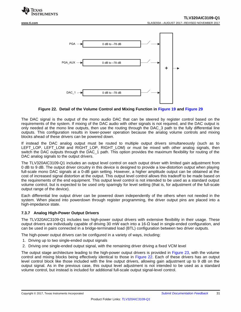
Figure 22. Detail of the Volume Control and Mixing Function in Figure 19 and Figure 29
The DAC signal is the output of the mono audio DAC that can be steered by register control based on therequirements of the system. If mixing of the DAC audio with other signals is not required, and the DAC output isonly needed at the mono line outputs, then use the routing through the DAC_3 path to the fully differential lineoutputs. This configuration results in lower-power operation because the analog volume controls and mixingblocks ahead of these drivers can be powered down.
If instead the DAC analog output must be routed to multiple output drivers simultaneously (such as toLEFT_LOP, LEFT_LOM and RIGHT_LOP, RIGHT_LOM) or must be mixed with other analog signals, thenswitch the DAC outputs through the DAC_1 path. This option provides the maximum flexibility for routing of theDAC analog signals to the output drivers.
The TLV320AIC3109-Q1 includes an output level control on each output driver with limited gain adjustment from0 dB to 9 dB. The output driver circuitry in this device is designed to provide a low-distortion output when playingfull-scale mono DAC signals at a 0-dB gain setting. However, a higher amplitude output can be obtained at thecost of increased signal distortion at the output. This output level control allows this tradeoff to be made based onthe requirements of the end equipment. This output level control is not intended to be used as a standard outputvolume control, but is expected to be used only sparingly for level setting (that is, for adjustment of the full-scaleoutput range of the device).
Each differential line output driver can be powered down independently of the others when not needed in thesystem. When placed into powerdown through register programming, the driver output pins are placed into ahigh-impedance state.
7.3.7 Analog High-Power Output DriversThe TLV320AIC3109-Q1 includes two high-power output drivers with extensive flexibility in their usage. Theseoutput drivers are individually capable of driving 30 mW each into a 16-Ω load in single-ended configuration, andcan be used in pairs connected in a bridge-terminated load (BTL) configuration between two driver outputs.
The high-power output drivers can be configured in a variety of ways, including:1. Driving up to two single-ended output signals2. Driving one single-ended output signal, with the remaining driver driving a fixed VCM level
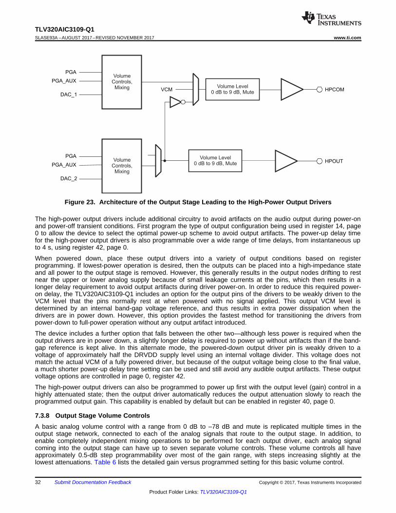
The output stage architecture leading to the high-power output drivers is provided in Figure 23, with the volumecontrol and mixing blocks being effectively identical to those in Figure 22. Each of these drivers has an outputlevel control block like those included with the line output drivers, allowing gain adjustment up to 9 dB on theoutput signal. As in the previous case, this output level adjustment is not intended to be used as a standardvolume control, but instead is included for additional full-scale output signal-level control.
VCM HPCOM
HPOUTPGA
PGA
DAC_2
DAC_1
PGA_AUX
PGA_AUX
VolumeControls,Mixing
VolumeControls,Mixing Volume Level
0 dB to 9 dB, Mute
Volume Level0 dB to 9 dB, Mute
32
TLV320AIC3109-Q1SLASE93A –AUGUST 2017–REVISED NOVEMBER 2017 www.ti.com
Product Folder Links: TLV320AIC3109-Q1
Submit Documentation Feedback Copyright © 2017, Texas Instruments Incorporated
Figure 23. Architecture of the Output Stage Leading to the High-Power Output Drivers
The high-power output drivers include additional circuitry to avoid artifacts on the audio output during power-onand power-off transient conditions. First program the type of output configuration being used in register 14, page0 to allow the device to select the optimal power-up scheme to avoid output artifacts. The power-up delay timefor the high-power output drivers is also programmable over a wide range of time delays, from instantaneous upto 4 s, using register 42, page 0.
When powered down, place these output drivers into a variety of output conditions based on registerprogramming. If lowest-power operation is desired, then the outputs can be placed into a high-impedance stateand all power to the output stage is removed. However, this generally results in the output nodes drifting to restnear the upper or lower analog supply because of small leakage currents at the pins, which then results in alonger delay requirement to avoid output artifacts during driver power-on. In order to reduce this required power-on delay, the TLV320AIC3109-Q1 includes an option for the output pins of the drivers to be weakly driven to theVCM level that the pins normally rest at when powered with no signal applied. This output VCM level isdetermined by an internal band-gap voltage reference, and thus results in extra power dissipation when thedrivers are in power down. However, this option provides the fastest method for transitioning the drivers frompower-down to full-power operation without any output artifact introduced.
The device includes a further option that falls between the other two—although less power is required when theoutput drivers are in power down, a slightly longer delay is required to power up without artifacts than if the band-gap reference is kept alive. In this alternate mode, the powered-down output driver pin is weakly driven to avoltage of approximately half the DRVDD supply level using an internal voltage divider. This voltage does notmatch the actual VCM of a fully powered driver, but because of the output voltage being close to the final value,a much shorter power-up delay time setting can be used and still avoid any audible output artifacts. These outputvoltage options are controlled in page 0, register 42.
The high-power output drivers can also be programmed to power up first with the output level (gain) control in ahighly attenuated state; then the output driver automatically reduces the output attenuation slowly to reach theprogrammed output gain. This capability is enabled by default but can be enabled in register 40, page 0.
7.3.8 Output Stage Volume ControlsA basic analog volume control with a range from 0 dB to –78 dB and mute is replicated multiple times in theoutput stage network, connected to each of the analog signals that route to the output stage. In addition, toenable completely independent mixing operations to be performed for each output driver, each analog signalcoming into the output stage can have up to seven separate volume controls. These volume controls all haveapproximately 0.5-dB step programmability over most of the gain range, with steps increasing slightly at thelowest attenuations. Table 6 lists the detailed gain versus programmed setting for this basic volume control.

33
TLV320AIC3109-Q1www.ti.com SLASE93A –AUGUST 2017–REVISED NOVEMBER 2017
Product Folder Links: TLV320AIC3109-Q1
Submit Documentation FeedbackCopyright © 2017, Texas Instruments Incorporated
Table 6. Output Stage Volume Control Settings and GainsGAIN
SETTINGANALOG
GAIN(dB)
GAINSETTING
ANALOGGAIN(dB)
GAINSETTING
ANALOGGAIN(dB)
GAINSETTING
ANALOGGAIN(dB)
0 0 30 –15 60 –30.1 90 –45.21 –0.5 31 –15.5 61 –30.6 91 –45.82 –1 32 –16 62 –31.1 92 –46.23 –1.5 33 –16.5 63 –31.6 93 –46.74 –2 34 –17 64 –32.1 94 –47.45 –2.5 35 –17.5 65 –32.6 95 –47.96 –3 36 –18 66 –33.1 96 –48.27 –3.5 37 –18.6 67 –33.6 97 –48.78 –4 38 –19.1 68 –34.1 98 –49.39 –4.5 39 –19.6 69 –34.6 99 –50
10 –5 40 –20.1 70 –35.1 100 –50.311 –5.5 41 –20.6 71 –35.7 101 –5112 –6 42 –21.1 72 –36.1 102 –51.413 –6.5 43 –21.6 73 –36.7 103 –51.814 –7 44 –22.1 74 –37.1 104 –52.215 –7.5 45 –22.6 75 –37.7 105 –52.716 –8 46 –23.1 76 –38.2 106 –53.717 –8.5 47 –23.6 77 –38.7 107 –54.218 –9 48 –24.1 78 –39.2 108 –55.319 –9.5 49 –24.6 79 –39.7 109 –56.720 –10 50 –25.1 80 –40.2 110 –58.321 –10.5 51 –25.6 81 –40.7 111 –60.222 –11 52 –26.1 82 –41.2 112 –62.723 –11.5 53 –26.6 83 –41.7 113 –64.324 –12 54 –27.1 84 –42.2 114 –66.225 –12.5 55 –27.6 85 –42.7 115 –68.726 –13 56 –28.1 86 –43.2 116 –72.227 –13.5 57 –28.6 87 –43.8 117 –78.328 –14 58 –29.1 88 –44.3 118–127 Mute29 –14.5 59 –29.6 89 –44.8 — —
7.3.9 Input Impedance and VCM ControlThe TLV320AIC3109-Q1 includes several programmable settings to control analog input pins, particularly whenthese inputs are not selected for connection to a PGA. The default option allows unselected inputs to be put intoa high-impedance state such that the input impedance of the device is extremely high. However, the pins on thedevice do include protection diode circuits connected to AVDD and AVSS. Thus, if any voltage is driven onto apin approximately one diode drop (~0.6 V) above AVDD or one diode drop below AVSS, these protection diodesbegin conducting current, resulting in an effective impedance that no longer appears as a high-impedance state.
In most cases, ac-couple the analog input pins on the TLV320AIC3109-Q1 to the analog input sources, except ifan ADC is used for dc voltage measurement. The ac-coupling capacitor causes a high-pass filter pole to beinserted into the analog signal path, so the size of the capacitor must be chosen to move that filter polesufficiently low in frequency to cause minimal effect on the processed analog signal. The input impedance of theanalog inputs when selected for connection to a PGA varies with the setting of the input level control, starting atapproximately 20 kΩ with an input level control setting of 0 dB, and increasing to approximately 80 kΩ when theinput level control is set at –12 dB. For example, using a 0.1-μF ac-coupling capacitor at an analog input resultsin a high-pass filter pole of 80 Hz when the 0-dB input level control setting is selected.
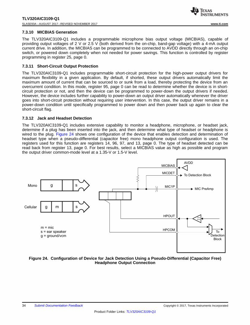
MICBIAS
MIC1P
HPOUT
ToDetection
Block
HPCOM
MICDETTo Detection Block
MIC PreAmps
sg m
gMono
Cellular
m = mics = ear speakerg = ground/vcm
AVDD
PwrAmp
34
TLV320AIC3109-Q1SLASE93A –AUGUST 2017–REVISED NOVEMBER 2017 www.ti.com
Product Folder Links: TLV320AIC3109-Q1
Submit Documentation Feedback Copyright © 2017, Texas Instruments Incorporated
7.3.10 MICBIAS GenerationThe TLV320AIC3109-Q1 includes a programmable microphone bias output voltage (MICBIAS), capable ofproviding output voltages of 2 V or 2.5 V (both derived from the on-chip, band-gap voltage) with a 4-mA outputcurrent drive. In addition, the MICBIAS can be programmed to be connected to AVDD directly through an on-chipswitch, or powered down completely when not needed for power savings. This function is controlled by registerprogramming in register 25, page 0.
7.3.11 Short-Circuit Output ProtectionThe TLV320AIC3109-Q1 includes programmable short-circuit protection for the high-power output drivers formaximum flexibility in a given application. By default, if shorted, these output drivers automatically limit themaximum amount of current that can be sourced to or sunk from a load, thereby protecting the device from anovercurrent condition. In this mode, register 95, page 0 can be read to determine whether the device is in short-circuit protection or not, and then the device can be programmed to power-down the output drivers if needed.However, the device includes further capability to power-down an output driver automatically whenever the drivergoes into short-circuit protection without requiring user intervention. In this case, the output driver remains in apower-down condition until specifically programmed to power down and then power back up again to clear theshort-circuit flag.
7.3.12 Jack and Headset DetectionThe TLV320AIC3109-Q1 includes extensive capability to monitor a headphone, microphone, or headset jack,determine if a plug has been inserted into the jack, and then determine what type of headset or headphone iswired to the plug. Figure 24 shows one configuration of the device that enables detection and determination ofheadset type when a pseudo-differential (capacitor free) mono headphone output configuration is used. Theregisters used for this function are registers 14, 96, 97, and 13, page 0. The type of headset detected can beread back from register 13, page 0. For best results, select a MICBIAS value as high as possible and programthe output driver common-mode level at a 1.35-V or 1.5-V level.
Figure 24. Configuration of Device for Jack Detection Using a Pseudo-Differential (Capacitor Free)Headphone Output Connection

HPCOM
HPOUT
To Detection Block
MIC PreAmp
s
sg m
sgMono
Cellular
m = mics = ear speakerg = ground/vcm
AVDDMICBIAS
MIC1P
MICDET
PwrAmp
PwrAmp
35
TLV320AIC3109-Q1www.ti.com SLASE93A –AUGUST 2017–REVISED NOVEMBER 2017
Product Folder Links: TLV320AIC3109-Q1
Submit Documentation FeedbackCopyright © 2017, Texas Instruments Incorporated
Figure 25 shows a modified output configuration used when the output drivers are ac-coupled.
Figure 25. Configuration of Device for Jack Detection Using an AC-Coupled Mono Headphone OutputConnection
7.4 Device Functional Modes
7.4.1 Bypass Path ModeThe TLV320AIC3109-Q1 is a versatile device designed for low-power applications. In some cases, only a fewfeatures of the device are required. For these applications, the unused stages of the device must be powereddown to save power and use an alternate route. This path is called a bypass path. The bypass path modes letthe device save power by turning off unused stages (such as the ADC, DAC, and PGA).
7.4.1.1 ADC PGA Signal Bypass Path FunctionalityIn addition to the input bypass path described previously, the TLV320AIC3109-Q1 also includes the ability toroute the ADC PGA output signals past the ADC for mixing with other analog signals and then for directconnection to the output drivers. These bypass functions are described in more detail in the Analog FullyDifferential Line Output Drivers and Analog High-Power Output Drivers sections.

LEFT_LOP
RIGHT_LOP
LEFT_LOM
RIGHT_LOM
SW-L0
SW-R0
SW-L3
SW-R3
SW-L1
SW-R1
SW-L4
SW-R4
MIC1P/LINE1P
MIC2P/LINE2P
MIC1M/LINE1M
MIC2M/LINE2M
LINE1P
LINE2P
LINE1M
LINE2M
B0174-01
36
TLV320AIC3109-Q1SLASE93A –AUGUST 2017–REVISED NOVEMBER 2017 www.ti.com
Product Folder Links: TLV320AIC3109-Q1
Submit Documentation Feedback Copyright © 2017, Texas Instruments Incorporated
Device Functional Modes (continued)7.4.1.2 Passive Analog Bypass During Power DownProgramming the TLV320AIC3109-Q1 to passive analog bypass occurs by configuring the output stage switchesfor passthrough. Figure 26 shows that this process is done by opening switches SW-L0, SW-L3, SW-R0, andSW-R3 and closing either SW-L1 and SW-R1. Programming this mode is done by writing to register 108, page 0.
Connecting the MIC1P/LINE1P input signal to the LEFT_LOP pin is done by closing SW-L1 and opening SW-L0;this action is done by writing a 1 to bit 0 in register 108, page 0. Connecting the MIC1M/LINE1M input signal tothe LEFT_LOM pin is done by closing SW-L4 and opening SW-L3; this action is done by writing a 1 to bit 1 inregister 108, page 0.
Connecting the MIC2P/LINE2P input signal to the RIGHT_LOP pin is done by closing SW-R1 and opening SW-R0; this action is done by writing a 1 to bit 4 in register 108, page 0. Figure 26 shows a diagram of the passiveanalog bypass mode configuration.
Figure 26. Passive Analog Bypass Mode Configuration

Digital Audio Data Serial Interface
ADC+
DIN
DO
UT
BC
LK
WC
LK
DIN
DO
UT
AGC Record Path
DigitalFilters
SW-D1
SW-D2
Analog InputsPGA
0 dB–59.5 dB,0.5-dB Steps
VolumeControl
DACPowered
Down
DAC
B0173-01
37
TLV320AIC3109-Q1www.ti.com SLASE93A –AUGUST 2017–REVISED NOVEMBER 2017
Product Folder Links: TLV320AIC3109-Q1
Submit Documentation FeedbackCopyright © 2017, Texas Instruments Incorporated
Device Functional Modes (continued)7.4.2 Digital Audio Processing for Record PathIn applications where record-only is selected and the DAC is powered down, the playback path signal processingblocks can be used in the ADC record path. These filtering blocks can support high-pass, low-pass, band-pass,or notch filtering. In this mode, the record-only path has switches SW-D1 and SW-D2 closed, and reroutes theADC output data through the digital signal processing blocks. Because the DAC digital signal processing blocksare being re-used, naturally the addresses of these digital filter coefficients are the same as for the DAC digitalprocessing and are located in registers 1–26, page 1. This record-only mode is enabled by powering down theDAC by writing to bit 7 in register 37, page 0 (where bit 7 = 0). Next, enable the digital filter pathway for the ADCby writing a 1 to bit 3 in register 107, page 0. (This pathway is only enabled if the DAC is powered down.)Figure 27 shows the record-only path.
Figure 27. Record-Only Mode With Digital Processing Path Enabled

SDA
SCL
tHD-STA
0.9 s³ m
tSU-STO
0.9 s³ m
P S
tSU-STA
0.9 s³ m
Sr
tHD-STA
0.9 s³ m
S
T0114-02
38
TLV320AIC3109-Q1SLASE93A –AUGUST 2017–REVISED NOVEMBER 2017 www.ti.com
Product Folder Links: TLV320AIC3109-Q1
Submit Documentation Feedback Copyright © 2017, Texas Instruments Incorporated
7.5 Programming
7.5.1 I2C Control InterfaceThe TLV320AIC3109-Q1 supports the I2C control protocol using 7-bit addressing and is capable of both standardand fast modes. As illustrated in Figure 28, the minimum timing for each tHD-STA, tSU-STA, and tSU-STO is 0.9 μs forI2C fast mode. The TLV320AIC3109-Q1 responds to the I2C address of 001 1000. I2C is a two-wire, open-draininterface supporting multiple devices and masters on a single bus. Devices on the I2C bus only drive the buslines low by connecting the lines to ground; the devices never drive the bus lines high. Instead, the bus wires arepulled high by pullup resistors so the bus wires are high when not being driven low by a device. This way twodevices cannot conflict; if two devices drive the bus simultaneously, there is no driver contention.
Figure 28. I2C Interface Timing
Communication on the I2C bus always takes place between two devices, one acting as the master and the otheracting as the slave. Both masters and slaves can read and write, but slaves can only do so under the direction ofthe master. Some I2C devices can act as masters or slaves, but the TLV320AIC3109-Q1 can only act as a slavedevice.
An I2C bus consists of two lines, SDA and SCL. SDA carries data; SCL provides the clock. All data aretransmitted across the I2C bus in groups of eight bits. To send a bit on the I2C bus, the SDA line is driven to theappropriate level when SCL is low (a low on SDA indicates the bit is zero; a high indicates the bit is one). Whenthe SDA line settles, the SCL line is brought high then low. This pulse on SCL clocks the SDA bit into thereceiver shift register.
The I2C bus is bidirectional: the SDA line is used both for transmitting and receiving data. When a master readsfrom a slave, the slave drives the data line; when a master sends to a slave, the master drives the data line.Under normal circumstances the master drives the clock line.
Most of the time the bus is idle, no communication is taking place, and both lines are high. When communicationis taking place, the bus is active. Only master devices can start a communication by causing a START conditionon the bus. Normally, the data line is only allowed to change state when the clock line is low. If the data linechanges state when the clock line is high, then the data line state is either a START condition or a STOPcondition. A START condition is when the clock line is high and the data line goes from high to low. A STOPcondition is when the clock line is high and the data line goes from low to high.
After the master issues a START condition, the master sends a byte that indicates which slave device tocommunicate with. This byte is called the address byte. Each device on an I2C bus has a unique 7-bit address.(Slaves can also have 10-bit addresses; see the I2C specification for details.) The master sends an address inthe address byte with a bit indicating whether to read from or write to the slave device.
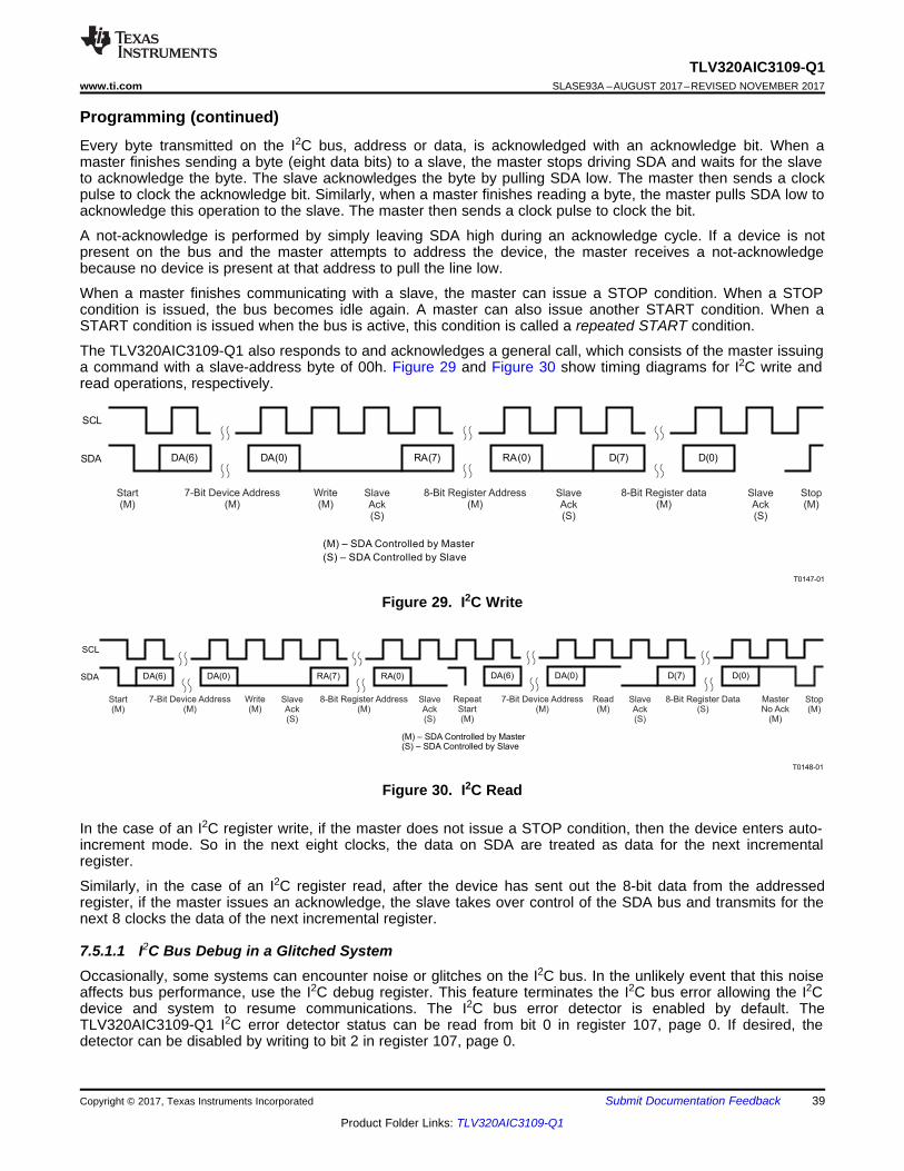
DA(6) DA(0) RA(7) RA(0)SDA
SCL
DA(6) DA(0) D(7) D(0)
(M) – SDA Controlled by Master(S) – SDA Controlled by Slave
Start(M)
Write(M)
SlaveAck(S)
SlaveAck(S)
SlaveAck(S)
MasterNo Ack
(M)
Stop(M)
RepeatStart(M)
Read(M)
7-Bit Device Address(M)
8-Bit Register Address(M)
8-Bit Register Data(S)
7-Bit Device Address(M)
T0148-01
DA(6) DA(0) RA(7) RA(0) D(7) D(0)
T0147-01
SDA
SCL
(M) – SDA Controlled by Master
(S) – SDA Controlled by Slave
Start(M)
Write(M)
SlaveAck(S)
SlaveAck(S)
SlaveAck(S)
Stop(M)
7-Bit Device Address(M)
8-Bit Register Address(M)
8-Bit Register data(M)
39
TLV320AIC3109-Q1www.ti.com SLASE93A –AUGUST 2017–REVISED NOVEMBER 2017
Product Folder Links: TLV320AIC3109-Q1
Submit Documentation FeedbackCopyright © 2017, Texas Instruments Incorporated
Programming (continued)Every byte transmitted on the I2C bus, address or data, is acknowledged with an acknowledge bit. When amaster finishes sending a byte (eight data bits) to a slave, the master stops driving SDA and waits for the slaveto acknowledge the byte. The slave acknowledges the byte by pulling SDA low. The master then sends a clockpulse to clock the acknowledge bit. Similarly, when a master finishes reading a byte, the master pulls SDA low toacknowledge this operation to the slave. The master then sends a clock pulse to clock the bit.
A not-acknowledge is performed by simply leaving SDA high during an acknowledge cycle. If a device is notpresent on the bus and the master attempts to address the device, the master receives a not-acknowledgebecause no device is present at that address to pull the line low.
When a master finishes communicating with a slave, the master can issue a STOP condition. When a STOPcondition is issued, the bus becomes idle again. A master can also issue another START condition. When aSTART condition is issued when the bus is active, this condition is called a repeated START condition.
The TLV320AIC3109-Q1 also responds to and acknowledges a general call, which consists of the master issuinga command with a slave-address byte of 00h. Figure 29 and Figure 30 show timing diagrams for I2C write andread operations, respectively.
Figure 29. I2C Write
Figure 30. I2C Read
In the case of an I2C register write, if the master does not issue a STOP condition, then the device enters auto-increment mode. So in the next eight clocks, the data on SDA are treated as data for the next incrementalregister.
Similarly, in the case of an I2C register read, after the device has sent out the 8-bit data from the addressedregister, if the master issues an acknowledge, the slave takes over control of the SDA bus and transmits for thenext 8 clocks the data of the next incremental register.
7.5.1.1 I2C Bus Debug in a Glitched SystemOccasionally, some systems can encounter noise or glitches on the I2C bus. In the unlikely event that this noiseaffects bus performance, use the I2C debug register. This feature terminates the I2C bus error allowing the I2Cdevice and system to resume communications. The I2C bus error detector is enabled by default. TheTLV320AIC3109-Q1 I2C error detector status can be read from bit 0 in register 107, page 0. If desired, thedetector can be disabled by writing to bit 2 in register 107, page 0.

40
TLV320AIC3109-Q1SLASE93A –AUGUST 2017–REVISED NOVEMBER 2017 www.ti.com
Product Folder Links: TLV320AIC3109-Q1
Submit Documentation Feedback Copyright © 2017, Texas Instruments Incorporated
7.6 Register Maps
7.6.1 Register Map StructureThe register map of the TLV320AIC3109-Q1 consists of two pages of registers, with each page containing 128registers. The register at address zero on each page is used as a page-control register and writing to this registerdetermines the active page for the device. All subsequent read/write operations access the page that is active atthe time unless a register write is performed to change the active page. The active page defaults to page 0 ondevice reset.
Table 7 lists the different access codes used in the TLV320AIC3109-Q1 registers.
Table 7. TLV320AIC3109-Q1 Access Type CodesAccess Type Code DescriptionR R ReadR-W R/W Read or writeW W Write-n Value after reset or the default
value
The control registers for the TLV320AIC3109-Q1 are described in this section. All registers are 8 bits in width,with bit 7 referring to the most-significant bit of each register and bit 0 referring to the least-significant bit. Table 8lists the registers for page 0 and page 1.
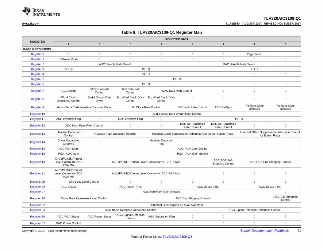
TLV320AIC3109-Q1www.ti.com SLASE93A –AUGUST 2017–REVISED NOVEMBER 2017
41
Product Folder Links: TLV320AIC3109-Q1
Submit Documentation FeedbackCopyright © 2017, Texas Instruments Incorporated
Table 8. TLV320AIC3109-Q1 Register Map
REGISTERREGISTER DATA
7 6 5 4 3 2 1 0
PAGE 0 REGISTERS
Register 0 0 0 0 0 0 0 Page Select
Register 1 Software Reset 0 0 0 0 0 0 0
Register 2 ADC Sample Rate Select DAC Sample Rate Select
Register 3 PLL Q PLL Q PLL P
Register 4 PLL J 0 0
Register 5 PLL D
Register 6 PLL D 0 0
Register 7 fS(ref) Setting DAC Dual-RateControl
DAC Data PathControl DAC Data Path Control 0 0 0
Register 8 Word ClockDirectional Control
Serial Output DataDriver
Bit, Word Clock DriveControl
Bit, Word Clock DriveControl 0 0 0 0
Register 9 Audio Serial Data Interface Transfer Mode Bit Clock Rate Control Bit Clock Rate Control ADC Re-Sync Re-Sync MuteBehavior
Re-Sync MuteBehavior
Register 10 Audio Serial Data Word Offset Control
Register 11 ADC Overflow Flag 0 DAC Overflow Flag 0 PLL R
Register 12 ADC High-Pass Filter Control 0 0 DAC De- EmphasisFilter Control
DAC De- EmphasisFilter Control 0 0
Register 13 Headset DetectionControl Headset Type Detection Results Headset Glitch Suppression Debounce Control for Button Press Headset Glitch Suppression Debounce Control
for Button Press
Register 14 Driver CapacitiveCoupling 0 0 Headset Detection
Flag 0 0 0 0
Register 15 ADC PGA Mute ADC PGA Gain Setting
Register 16 PGA_AUX Mute PGA _AUX Gain Setting
Register 19MIC1P/LINE1P InputLevel Control for ADC
PGA MixMIC1P/LINE1P Input Level Control for ADC PGA Mix ADC PGA Soft-
Stepping Control ADC PGA Soft-Stepping Control
Register 21MIC2P/LINE2P InputLevel Control for ADC
PGA MixMIC2P/LINE2P Input Level Control for ADC PGA Mix 0 0 0
Register 25 MICBIAS Level Control 0 0 0 0 0 0
Register 26 AGC Enable AGC Attack Time AGC Decay Time AGC Decay Time
Register 27 AGC Maximum Gain Allowed 0
Register 28 Noise Gate Hysteresis Level Control AGC Clip Stepping Control AGC Clip SteppingControl
Register 32 Channel Gain Applied by AGC Algorithm
Register 34 AGC Noise Detection Debounce Control AGC Signal Detection Debounce Control
Register 36 ADC PGA Status ADC Power Status AGC Signal DetectionStatus AGC Saturation Flag 0 0 0 0
Register 37 DAC Power Control 0 0 0 0 0 0 0

TLV320AIC3109-Q1SLASE93A –AUGUST 2017–REVISED NOVEMBER 2017 www.ti.com
42
Product Folder Links: TLV320AIC3109-Q1
Submit Documentation Feedback Copyright © 2017, Texas Instruments Incorporated
Table 8. TLV320AIC3109-Q1 Register Map (continued)
REGISTERREGISTER DATA
7 6 5 4 3 2 1 0
Register 38 0 0 HPCOM Output Driver Configuration Control Short-CircuitProtection Control
Short-CircuitProtection Mode
Control0
Register 40 Output Common-Mode Voltage Control 0 0 0 0 Output Volume Control Soft- Stepping
Register 41 DAC Output Switching Control 0 0 0 0 0 0
Register 42 Output Driver Power-On Delay Control Driver Ramp-Up Step Timing ControlWeak Output
Common-ModeVoltage Control
0
Register 43 DAC Digital Mute DAC Digital Volume Control Setting
Register 60 PGA Output RoutingControl PGA to HPOUT Analog Volume Control
Register 61 DAC_1 OutputRouting Control DAC_1 to HPOUT Analog Volume Control
Register 63 PGA_AUX OutputRouting Control PGA_AUX to HPOUT Analog Volume Control
Register 65 HPOUT Output Level Control HPOUT Mute HPOUT Power- DownDrive Control
HPOUT VolumeControl Status
HPOUT PowerControl
Register 67 PGA Output RoutingControl PGA to HPCOM Analog Volume Control
Register 68 DAC_1 OutputRouting Control DAC_1 to HPCOM Analog Volume Control
Register 70 PGA_AUX OutputRouting Control PGA_AUX to HPCOM Analog Volume Control
Register 72 HPCOM Output Level Control HPCOM Mute HPCOM VolumeControl Status
HPCOM VolumeControl Status
HPCOM PowerControl
Register 81 PGA Output RoutingControl PGA to LEFT_LOP/M Analog Volume Control
Register 82 DAC_1 OutputRouting Control DAC_1 to LEFT_LOP/M Analog Volume Control
Register 84 PGA_AUX OutputRouting Control PGA_AUX to LEFT_LOP/M Analog Volume Control
Register 86 LEFT_LOP/M Output Level Control LEFT_LOP/M Mute 0 LEFT_LOP/M VolumeControl Status
LEFT_LOP/M PowerStatus
Register 88 PGA Output RoutingControl DAC_1 Output Routing Control
Register 89 DAC_1 OutputRouting Control DAC_1 to RIGHT_LOP/M Analog Volume Control
Register 91 PGA_AUX OutputRouting Control PGA_AUX to RIGHT_LOP/M Analog Volume Control
Register 93 RIGHT_LOP/M Output Level Control RIGHT_LOP/M Mute 0RIGHT_LOP/MVolume Control
Status
RIGHT_LOP/M PowerStatus

TLV320AIC3109-Q1www.ti.com SLASE93A –AUGUST 2017–REVISED NOVEMBER 2017
43
Product Folder Links: TLV320AIC3109-Q1
Submit Documentation FeedbackCopyright © 2017, Texas Instruments Incorporated
Table 8. TLV320AIC3109-Q1 Register Map (continued)
REGISTERREGISTER DATA
7 6 5 4 3 2 1 0
Register 94 DAC Power Status 0 0 LEFT_LOP/M PowerStatus
RIGHT_LOP/M PowerStatus 0 HPOUT Driver Power
Status 0
Register 95 0 HPOUT Short- CircuitDetection Status 0 HPCOM Short- Circuit
Detection Status 0 HPCOM Power Status 0 0
Register 96 0 HPOUT Short- CircuitDetection Status 0 HPCOM Short- Circuit
Detection Status 0 Headset DetectionStatus
ADC AGC Noise GateStatus 0
Register 97 0 HPOUT Short- CircuitDetection Status 0 HPCOM Short- Circuit
Detection Status 0 Headset DetectionStatus
ADC AGC Noise GateStatus 0
Register 101 0 0 0 0 0 0 0 CODEC_CLKINSource Selection
Register 102 CLKDIV_IN Source Selection PLLCLK_IN Source Selection 0 0 1 0
Register 103 Attack Time RegisterSelection Baseline AGC Attack Time Multiplication Factor for Baseline AGC 0 0
Register 104 Decay Time RegisterSelection Baseline AGC Decay Time Multiplication Factor for Baseline AGC 0 0
Register 107Channel High- Pass
Filter CoefficientSelection
0 0 0ADC Digital Output toProgrammable Filter
Path SelectionI2C Bus Condition
Detector 0 I2C Bus ErrorDetection Status
Register 108 0 0 LINE1RM PathSelection
LINE1RP PathSelection 0 0 LINE1LM Path
SelectionLINE1LP Path
Selection
Register 109 DAC Current Adjustment 0 0 0 0 0 0
PAGE 1 REGISTERS
Register 0 0 0 0 0 0 0 0 Page Select Bit
Register 1 Audio Effects Filter N0 Coefficient MSB
Register 2 Audio Effects Filter N0 Coefficient LSB
Register 3 Audio Effects Filter N1 Coefficient MSB
Register 4 Audio Effects Filter N1 Coefficient LSB
Register 5 Audio Effects Filter N2 Coefficient MSB
Register 6 Audio Effects Filter N2 Coefficient LSB
Register 7 Audio Effects Filter N3 Coefficient MSB
Register 8 Audio Effects Filter N3 Coefficient LSB
Register 9 Audio Effects Filter N4 Coefficient MSB
Register 10 Audio Effects Filter N4 Coefficient LSB
Register 11 Audio Effects Filter N5 Coefficient MSB
Register 12 Audio Effects Filter N5 Coefficient LSB
Register 13 Audio Effects Filter D1 Coefficient MSB
Register 14 Audio Effects Filter D1 Coefficient LSB
Register 15 Audio Effects Filter D2 Coefficient MSB
Register 16 Audio Effects Filter D2 Coefficient LSB

TLV320AIC3109-Q1SLASE93A –AUGUST 2017–REVISED NOVEMBER 2017 www.ti.com
44
Product Folder Links: TLV320AIC3109-Q1
Submit Documentation Feedback Copyright © 2017, Texas Instruments Incorporated
Table 8. TLV320AIC3109-Q1 Register Map (continued)
REGISTERREGISTER DATA
7 6 5 4 3 2 1 0
Register 17 Audio Effects Filter D4 Coefficient MSB
Register 18 Audio Effects Filter D4 Coefficient LSB
Register 19 Audio Effects Filter D5 Coefficient MSB
Register 20 Audio Effects Filter D5 Coefficient LSB
Register 21 De-Emphasis Filter N0 Coefficient MSB
Register 22 De-Emphasis Filter N0 Coefficient LSB
Register 23 De-Emphasis Filter N1 Coefficient MSB
Register 24 De-Emphasis Filter N1 Coefficient LSB
Register 25 De-Emphasis Filter D1 Coefficient MSB
Register 26 De-Emphasis Filter D1 Coefficient LSB
Register 65 ADC High-Pass Filter N0 Coefficient MSB
Register 66 Channel ADC High-Pass Filter N0 Coefficient LSB
Register 67 Channel ADC High-Pass Filter N1 Coefficient MSB
Register 68 Channel ADC High-Pass Filter N1 Coefficient LSB
Register 69 Channel ADC High-Pass Filter D1 Coefficient MSB
Register 70 Channel ADC High-Pass Filter D1 Coefficient LSB

45
TLV320AIC3109-Q1www.ti.com SLASE93A –AUGUST 2017–REVISED NOVEMBER 2017
Product Folder Links: TLV320AIC3109-Q1
Submit Documentation FeedbackCopyright © 2017, Texas Instruments Incorporated
7.6.2 Page 0 RegistersThese registers are held within page 0.
7.6.2.1 Register 0: Page Select (address = 0h) [reset = 0000 0000], Page 0
Figure 31. Register 0
7 6 5 4 3 2 1 00 0 0 0 0 0 0 Page Select
R-0h R-0h R-0h R-0h R-0h R-0h R-0h R/W-0h
Table 9. Register 0 Field DescriptionsBit Field Type Reset Description7:1 Reserved R 0h Reserved. Always write zeros to these bits.0 Page Select R/W 0h Page select bit.
Writing a 0 to this bit sets page 0 as the active page for thefollowing register accesses. Writing a 1 to this bit sets page 1 asthe active page for the following register accesses. This registerbit is recommended to be read back after each write to ensurethat the proper page is being accessed for future register readsor writes.
7.6.2.2 Register 1: Software Reset Register (address = 1h) [reset = 0000 0000], Page 0
Figure 32. Register 1
7 6 5 4 3 2 1 0Software Reset 0 0 0 0 0 0 0
W-0h W-0h W-0h W-0h W-0h W-0h W-0h W-0h
Table 10. Register 1 Field DescriptionsBit Field Type Reset Description7 Software Reset W 0h Software reset bit.
0 : Don’t care1 : Self-clearing software reset
6:0 Reserved W 0h Reserved. Always write zeros to these bits.
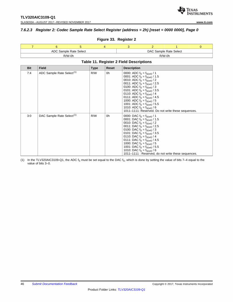
46
TLV320AIC3109-Q1SLASE93A –AUGUST 2017–REVISED NOVEMBER 2017 www.ti.com
Product Folder Links: TLV320AIC3109-Q1
Submit Documentation Feedback Copyright © 2017, Texas Instruments Incorporated
7.6.2.3 Register 2: Codec Sample Rate Select Register (address = 2h) [reset = 0000 0000], Page 0
Figure 33. Register 2
7 6 5 4 3 2 1 0ADC Sample Rate Select DAC Sample Rate Select
R/W-0h R/W-0h
(1) In the TLV320AIC3109-Q1, the ADC fS must be set equal to the DAC fS, which is done by setting the value of bits 7–4 equal to thevalue of bits 3–0.
Table 11. Register 2 Field DescriptionsBit Field Type Reset Description7:4 ADC Sample Rate Select (1) R/W 0h 0000: ADC fS = fS(ref) / 1
0001: ADC fS = fS(ref) / 1.50010: ADC fS = fS(ref) / 20011: ADC fS = fS(ref) / 2.50100: ADC fS = fS(ref) / 30101: ADC fS = fS(ref) / 3.50110: ADC fS = fS(ref) / 40111: ADC fS = fS(ref) / 4.51000: ADC fS = fS(ref) / 51001: ADC fS = fS(ref) / 5.51010: ADC fS = fS(ref) / 61011–1111: Reserved. Do not write these sequences.
3:0 DAC Sample Rate Select (1) R/W 0h 0000: DAC fS = fS(ref) / 10001: DAC fS = fS(ref) / 1.50010: DAC fS = fS(ref) / 20011: DAC fS = fS(ref) / 2.50100: DAC fS = fS(ref) / 30101: DAC fS = fS(ref) / 3.50110: DAC fS = fS(ref) / 40111: DAC fS = fS(ref) / 4.51000: DAC fS = fS(ref) / 51001: DAC fS = fS(ref) / 5.51010: DAC fS = fS(ref) / 61011–1111 : Reserved, do not write these sequences.
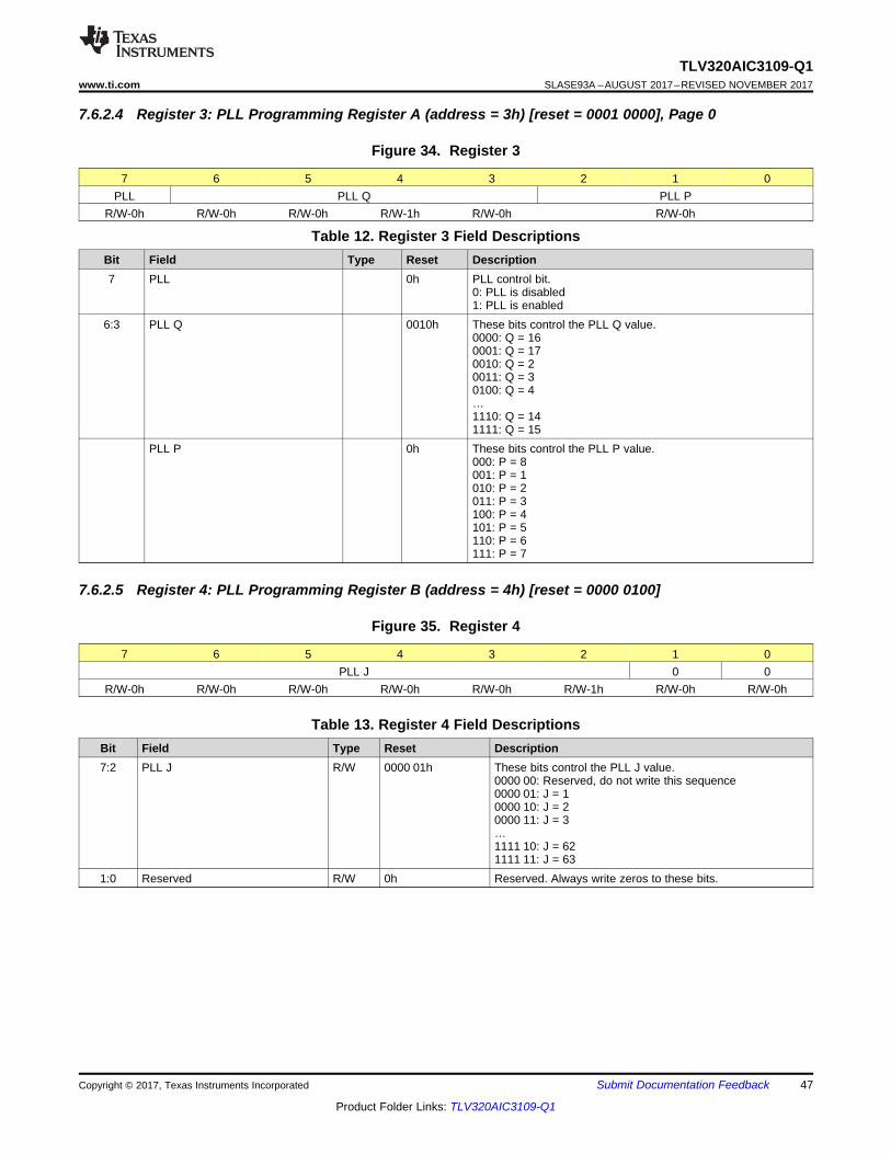
47
TLV320AIC3109-Q1www.ti.com SLASE93A –AUGUST 2017–REVISED NOVEMBER 2017
Product Folder Links: TLV320AIC3109-Q1
Submit Documentation FeedbackCopyright © 2017, Texas Instruments Incorporated
7.6.2.4 Register 3: PLL Programming Register A (address = 3h) [reset = 0001 0000], Page 0
Figure 34. Register 3
7 6 5 4 3 2 1 0PLL PLL Q PLL P
R/W-0h R/W-0h R/W-0h R/W-1h R/W-0h R/W-0h
Table 12. Register 3 Field DescriptionsBit Field Type Reset Description7 PLL 0h PLL control bit.
0: PLL is disabled1: PLL is enabled
6:3 PLL Q 0010h These bits control the PLL Q value.0000: Q = 160001: Q = 170010: Q = 20011: Q = 30100: Q = 4…1110: Q = 141111: Q = 15
PLL P 0h These bits control the PLL P value.000: P = 8001: P = 1010: P = 2011: P = 3100: P = 4101: P = 5110: P = 6111: P = 7
7.6.2.5 Register 4: PLL Programming Register B (address = 4h) [reset = 0000 0100]
Figure 35. Register 4
7 6 5 4 3 2 1 0PLL J 0 0
R/W-0h R/W-0h R/W-0h R/W-0h R/W-0h R/W-1h R/W-0h R/W-0h
Table 13. Register 4 Field DescriptionsBit Field Type Reset Description7:2 PLL J R/W 0000 01h These bits control the PLL J value.
0000 00: Reserved, do not write this sequence0000 01: J = 10000 10: J = 20000 11: J = 3…1111 10: J = 621111 11: J = 63
1:0 Reserved R/W 0h Reserved. Always write zeros to these bits.
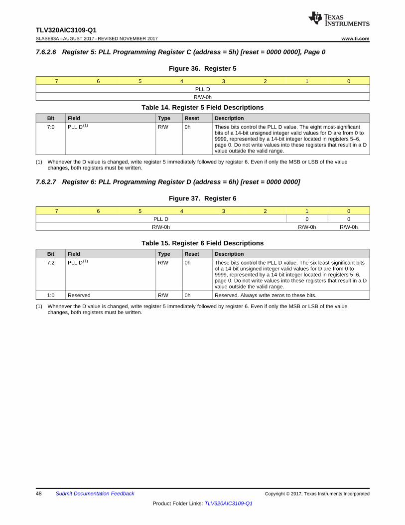
48
TLV320AIC3109-Q1SLASE93A –AUGUST 2017–REVISED NOVEMBER 2017 www.ti.com
Product Folder Links: TLV320AIC3109-Q1
Submit Documentation Feedback Copyright © 2017, Texas Instruments Incorporated
7.6.2.6 Register 5: PLL Programming Register C (address = 5h) [reset = 0000 0000], Page 0
Figure 36. Register 5
7 6 5 4 3 2 1 0PLL D
R/W-0h
(1) Whenever the D value is changed, write register 5 immediately followed by register 6. Even if only the MSB or LSB of the valuechanges, both registers must be written.
Table 14. Register 5 Field DescriptionsBit Field Type Reset Description7:0 PLL D (1) R/W 0h These bits control the PLL D value. The eight most-significant
bits of a 14-bit unsigned integer valid values for D are from 0 to9999, represented by a 14-bit integer located in registers 5–6,page 0. Do not write values into these registers that result in a Dvalue outside the valid range.
7.6.2.7 Register 6: PLL Programming Register D (address = 6h) [reset = 0000 0000]
Figure 37. Register 6
7 6 5 4 3 2 1 0PLL D 0 0
R/W-0h R/W-0h R/W-0h
(1) Whenever the D value is changed, write register 5 immediately followed by register 6. Even if only the MSB or LSB of the valuechanges, both registers must be written.
Table 15. Register 6 Field DescriptionsBit Field Type Reset Description7:2 PLL D (1) R/W 0h These bits control the PLL D value. The six least-significant bits
of a 14-bit unsigned integer valid values for D are from 0 to9999, represented by a 14-bit integer located in registers 5–6,page 0. Do not write values into these registers that result in a Dvalue outside the valid range.
1:0 Reserved R/W 0h Reserved. Always write zeros to these bits.
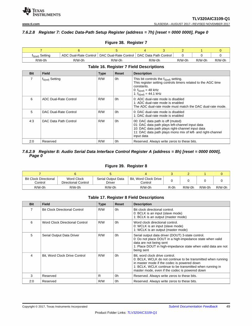
49
TLV320AIC3109-Q1www.ti.com SLASE93A –AUGUST 2017–REVISED NOVEMBER 2017
Product Folder Links: TLV320AIC3109-Q1
Submit Documentation FeedbackCopyright © 2017, Texas Instruments Incorporated
7.6.2.8 Register 7: Codec Data-Path Setup Register (address = 7h) [reset = 0000 0000], Page 0
Figure 38. Register 7
7 6 5 4 3 2 1 0fS(ref) Setting ADC Dual-Rate Control DAC Dual-Rate Control DAC Data Path Control 0 0 0
R/W-0h R/W-0h R/W-0h R/W-0h R/W-0h R/W-0h R/W-0h
Table 16. Register 7 Field DescriptionsBit Field Type Reset Description7 fS(ref) Setting R/W 0h This bit controls the fS(ref) setting.
This register setting controls timers related to the AGC timeconstants.0: fS(ref) = 48 kHz1: fS(ref) = 44.1 kHz
6 ADC Dual-Rate Control R/W 0h 0: ADC dual-rate mode is disabled1: ADC dual-rate mode is enabledThe ADC dual-rate mode must match the DAC dual-rate mode.
5 DAC Dual-Rate Control R/W 0h 0: DAC dual-rate mode is disabled1: DAC dual-rate mode is enabled
4:3 DAC Data Path Control R/W 0h 00: DAC data path is off (muted)01: DAC data path plays left-channel input data10: DAC data path plays right-channel input data11: DAC data path plays mono mix of left- and right-channelinput data
2:0 Reserved R/W 0h Reserved. Always write zeros to these bits.
7.6.2.9 Register 8: Audio Serial Data Interface Control Register A (address = 8h) [reset = 0000 0000],Page 0
Figure 39. Register 8
7 6 5 4 3 2 1 0Bit Clock Directional
ControlWord Clock
Directional ControlSerial Output Data
DriverBit, Word Clock Drive
Control 0 0 0 0
R/W-0h R/W-0h R/W-0h R/W-0h R-0h R/W-0h R/W-0h R/W-0h
Table 17. Register 8 Field DescriptionsBit Field Type Reset Description7 Bit Clock Directional Control R/W 0h Bit clock directional control.
0: BCLK is an input (slave mode)1: BCLK is an output (master mode)
6 Word Clock Directional Control R/W 0h Word clock directional control.0: WCLK is an input (slave mode)1: WCLK is an output (master mode)
5 Serial Output Data Driver R/W 0h Serial output data driver (DOUT) 3-state control.0: Do not place DOUT in a high-impedance state when validdata are not being sent1: Place DOUT in high-impedance state when valid data are notbeing sent
4 Bit, Word Clock Drive Control R/W 0h Bit, word clock drive control.0: BCLK, WCLK do not continue to be transmitted when runningin master mode if the codec is powered down1: BCLK, WCLK continue to be transmitted when running inmaster mode, even if the codec is powered down
3 Reserved R 0h Reserved. Always write zeros to these bits.2:0 Reserved R/W 0h Reserved. Always write zeros to these bits.
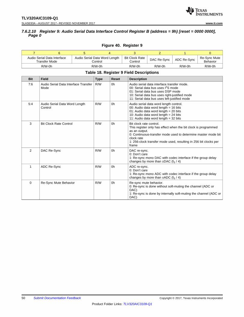
50
TLV320AIC3109-Q1SLASE93A –AUGUST 2017–REVISED NOVEMBER 2017 www.ti.com
Product Folder Links: TLV320AIC3109-Q1
Submit Documentation Feedback Copyright © 2017, Texas Instruments Incorporated
7.6.2.10 Register 9: Audio Serial Data Interface Control Register B (address = 9h) [reset = 0000 0000],Page 0
Figure 40. Register 9
7 6 5 4 3 2 1 0Audio Serial Data Interface
Transfer ModeAudio Serial Data Word Length
ControlBit Clock Rate
Control DAC Re-Sync ADC Re-Sync Re-Sync MuteBehavior
R/W-0h R/W-0h R/W-0h R/W-0h R/W-0h R/W-0h
Table 18. Register 9 Field DescriptionsBit Field Type Reset Description7:6 Audio Serial Data Interface Transfer
ModeR/W 0h Audio serial data interface transfer mode.
00: Serial data bus uses I2S mode01: Serial data bus uses DSP mode10: Serial data bus uses right-justified mode11: Serial data bus uses left-justified mode
5:4 Audio Serial Data Word LengthControl
R/W 0h Audio serial data word length control.00: Audio data word length = 16 bits01: Audio data word length = 20 bits10: Audio data word length = 24 bits11: Audio data word length = 32 bits
3 Bit Clock Rate Control R/W 0h Bit clock rate control.This register only has effect when the bit clock is programmedas an output.0: Continuous-transfer mode used to determine master mode bitclock rate1: 256-clock transfer mode used, resulting in 256 bit clocks perframe
2 DAC Re-Sync R/W 0h DAC re-sync.0: Don’t care1: Re-sync mono DAC with codec interface if the group delaychanges by more than ±DAC (fS / 4)
1 ADC Re-Sync R/W 0h ADC re-sync.0: Don’t care1: Re-sync mono ADC with codec interface if the group delaychanges by more than ±ADC (fS / 4)
0 Re-Sync Mute Behavior R/W 0h Re-sync mute behavior.0: Re-sync is done without soft-muting the channel (ADC orDAC)1: Re-sync is done by internally soft-muting the channel (ADC orDAC)
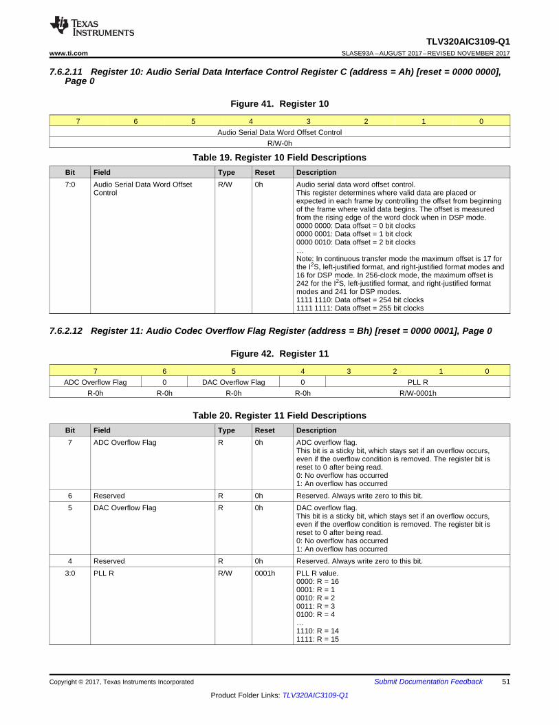
51
TLV320AIC3109-Q1www.ti.com SLASE93A –AUGUST 2017–REVISED NOVEMBER 2017
Product Folder Links: TLV320AIC3109-Q1
Submit Documentation FeedbackCopyright © 2017, Texas Instruments Incorporated
7.6.2.11 Register 10: Audio Serial Data Interface Control Register C (address = Ah) [reset = 0000 0000],Page 0
Figure 41. Register 10
7 6 5 4 3 2 1 0Audio Serial Data Word Offset Control
R/W-0h
Table 19. Register 10 Field DescriptionsBit Field Type Reset Description7:0 Audio Serial Data Word Offset
ControlR/W 0h Audio serial data word offset control.
This register determines where valid data are placed orexpected in each frame by controlling the offset from beginningof the frame where valid data begins. The offset is measuredfrom the rising edge of the word clock when in DSP mode.0000 0000: Data offset = 0 bit clocks0000 0001: Data offset = 1 bit clock0000 0010: Data offset = 2 bit clocks…Note: In continuous transfer mode the maximum offset is 17 forthe I2S, left-justified format, and right-justified format modes and16 for DSP mode. In 256-clock mode, the maximum offset is242 for the I2S, left-justified format, and right-justified formatmodes and 241 for DSP modes.1111 1110: Data offset = 254 bit clocks1111 1111: Data offset = 255 bit clocks
7.6.2.12 Register 11: Audio Codec Overflow Flag Register (address = Bh) [reset = 0000 0001], Page 0
Figure 42. Register 11
7 6 5 4 3 2 1 0ADC Overflow Flag 0 DAC Overflow Flag 0 PLL R
R-0h R-0h R-0h R-0h R/W-0001h
Table 20. Register 11 Field DescriptionsBit Field Type Reset Description7 ADC Overflow Flag R 0h ADC overflow flag.
This bit is a sticky bit, which stays set if an overflow occurs,even if the overflow condition is removed. The register bit isreset to 0 after being read.0: No overflow has occurred1: An overflow has occurred
6 Reserved R 0h Reserved. Always write zero to this bit.5 DAC Overflow Flag R 0h DAC overflow flag.
This bit is a sticky bit, which stays set if an overflow occurs,even if the overflow condition is removed. The register bit isreset to 0 after being read.0: No overflow has occurred1: An overflow has occurred
4 Reserved R 0h Reserved. Always write zero to this bit.3:0 PLL R R/W 0001h PLL R value.
0000: R = 160001: R = 10010: R = 20011: R = 30100: R = 4…1110: R = 141111: R = 15

52
TLV320AIC3109-Q1SLASE93A –AUGUST 2017–REVISED NOVEMBER 2017 www.ti.com
Product Folder Links: TLV320AIC3109-Q1
Submit Documentation Feedback Copyright © 2017, Texas Instruments Incorporated
7.6.2.13 Register 12: Audio Codec Digital Filter Control Register (address = Ch) [reset = 0000 0000],Page 0
Figure 43. Register 12
7 6 5 4 3 2 1 0ADC High-Pass Filter
Control 0 0 DAC Digital Effects FilterControl
DAC De-Emphasis FilterControl 0 0
R/W-0h R/W-0h R/W-0h R/W-0h R/W-0h R/W-0h R/W-0h R/W-0h
Table 21. Register 12 Field DescriptionsBit Field Type Reset Description7:6 ADC High-Pass Filter Control R/W 0h ADC high-pass filter control.
00: ADC high-pass filter disabled01: ADC high-pass filter –3-dB frequency = 0.0045 × ADC fS10:ADC high-pass filter –3-dB frequency = 0.0125 × ADC fS11: ADC high-pass filter –3-dB frequency = 0.025 × ADC fS
5:4 Reserved R/W 0h Reserved. Always write zeros to these bits.3 DAC Digital Effects Filter Control R/W 0h DAC digital effects filter control.
0: DAC digital effects filter disabled (bypassed)1: DAC digital effects filter enabled
2 DAC De-Emphasis Filter Control R/W 0h DAC de-emphasis filter control.0: DAC de-emphasis filter disabled (bypassed)1: DAC de-emphasis filter enabled
1:0 Reserved R/W 0h Reserved. Always write zeros to these bits.
7.6.2.14 Register 13: Headset/Button Press Detection Register A (address = Dh) [reset = 0000 0000],Page 0
Figure 44. Register 13
7 6 5 4 3 2 1 0
Headset Detection Control Headset Type DetectionResults
Headset Glitch Suppression DebounceControl for Jack Detection
Headset Glitch SuppressionDebounce Control for Button
PressR/W-0h R-0h R/W-0h R/W-0h
Table 22. Register 13 Field DescriptionsBit Field Type Reset Description7 Headset Detection Control R/W 0h Headset detection control.
0: Headset detection disabled1: Headset detection enabled
6:5 Headset Type Detection Results R 0h Headset type detection results.00: No headset detected01: Headset without microphone detected10: Ignore (reserved)11: Headset with microphone detected
4:2 Headset Glitch SuppressionDebounce Control for JackDetection
R/W 0h Headset glitch suppression debounce control for jack detection.000: Debounce = 16 ms (sampled with 2-ms clock)001: Debounce = 32 ms (sampled with 4-ms clock)010: Debounce = 64 ms (sampled with 8-ms clock)011: Debounce = 128 ms (sampled with 16-ms clock)100: Debounce = 256 ms (sampled with 32-ms clock)101: Debounce = 512 ms (sampled with 64-ms clock)110, 111: Reserved, do not write this bit sequence to theseregister bits
1:0 Headset Glitch SuppressionDebounce Control for Button Press
R/W 0h Headset glitch suppression debounce control for button press.00: Debounce = 0 ms01: Debounce = 8 ms (sampled with 1-ms clock)10: Debounce = 16 ms (sampled with 2-ms clock)11: Debounce = 32 ms (sampled with 4-ms clock)

53
TLV320AIC3109-Q1www.ti.com SLASE93A –AUGUST 2017–REVISED NOVEMBER 2017
Product Folder Links: TLV320AIC3109-Q1
Submit Documentation FeedbackCopyright © 2017, Texas Instruments Incorporated
7.6.2.15 Register 14: Headset/Button Press Detection Register B (address = Eh) [reset = 0000 0000],Page 0
Figure 45. Register 14
7 6 5 4 3 2 1 0Driver Capacitive
Coupling 0 0 Headset Detection Flag 0 0 0 0
R/W-0h R/W-0h R-0h R-0h R-0h R-0h R-0h R-0h
Table 23. Register 14 Field DescriptionsBit Field Type Reset Description7 Driver Capacitive Coupling R/W 0h Driver capacitive coupling.
0: Programs high-power outputs for capacitor-free driverconfiguration1: Programs high-power outputs for ac-coupled driverconfiguration
6 Reserved R/W 0h Reserved. Always write zero to this bit.5 Reserved R 0h Reserved. Always write zero to this bit.4 Headset Detection Flag R 0h Headset detection flag.
0: A headset is not detected1: A headset is detected
3:0 Reserved R 0h Reserved. Always write zeros to these bits
7.6.2.16 Register 15: ADC PGA Gain Control Register (address = Fh) [reset = 1000 0000], Page 0
Figure 46. Register 15
7 6 5 4 3 2 1 0ADC PGA Mute ADC PGA Gain Setting
R/W-1h R/W-0h
Table 24. Register 15 Field DescriptionsBit Field Type Reset Description7 ADC PGA Mute R/W 1h ADC PGA mute.
0: The ADC PGA is not muted1: The ADC PGA is muted
6:0 ADC PGA Gain Setting R/W 0h ADC PGA gain setting.000 0000: Gain = 0 dB000 0001: Gain = 0.5 dB000 0010: Gain = 1 dB…111 0110: Gain = 59 dB111 0111: Gain = 59.5 dB111 1000: Gain = 59.5 dB…111 1111: Gain = 59.5 dB

54
TLV320AIC3109-Q1SLASE93A –AUGUST 2017–REVISED NOVEMBER 2017 www.ti.com
Product Folder Links: TLV320AIC3109-Q1
Submit Documentation Feedback Copyright © 2017, Texas Instruments Incorporated
7.6.2.17 Register 16: Auxiliary PGA Gain Control Register (address = Fh) [reset = 1000 0000], Page 0
Figure 47. Register 16
7 6 5 4 3 2 1 0PGA_AUX Mute PGA _AUX Gain Setting
R/W-1h R/W-0h
Table 25. Register 16 Field DescriptionsBit Field Type Reset Description7 PGA_AUX Mute R/W 1h PGA_AUX mute.
0: The auxiliary PGA is not muted1: The auxiliary PGA is muted
6:0 PGA_AUX Gain Setting R/W 0h PGA_AUX gain setting.000 0000: Gain = 0 dB000 0001: Gain = 0.5 dB000 0010: Gain = 1 dB…111 0110: Gain = 59 dB111 0111: Gain = 59.5 dB111 1000: Gain = 59.5 dB…111 1111: Gain = 59.5 dB
7.6.2.18 Register 17–18: Reserved (address = 11h–12h) [reset = 1111 1111], Page 0
Figure 48. Register 17
7 6 5 4 3 2 1 01 1 1 1 1 1 1 1
R/W-1h R/W-1h R/W-1h R/W-1h R/W-1h R/W-1h R/W-1h R/W-1h
Table 26. Register 17 Field DescriptionsBit Field Type Reset Description7:0 Reserved R/W 1h Reserved. Always write ones to these bits.
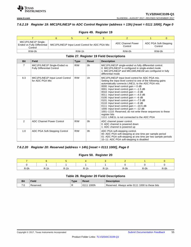
55
TLV320AIC3109-Q1www.ti.com SLASE93A –AUGUST 2017–REVISED NOVEMBER 2017
Product Folder Links: TLV320AIC3109-Q1
Submit Documentation FeedbackCopyright © 2017, Texas Instruments Incorporated
7.6.2.19 Register 19: MIC1P/LINE1P to ADC Control Register (address = 13h) [reset = 0111 1000], Page 0
Figure 49. Register 19
7 6 5 4 3 2 1 0MIC1P/LINE1P Single-
Ended vs Fully DifferentialControl
MIC1P/LINE1P Input Level Control for ADC PGA Mix ADC Channel PowerControl
ADC PGA Soft-SteppingControl
R/W-0h R/W-1h R/W-0h R/W-0h
Table 27. Register 19 Field DescriptionsBit Field Type Reset Description7 MIC1P/LINE1P Single-Ended vs
Fully Differential ControlR/W 0h MIC1P/LINE1P single-ended vs fully differential control.
0: MIC1P/LINE1P is configured in single-ended mode1: MIC1P/LINE1P and MIC1M/LINE1M are configured in fullydifferential mode
6:3 MIC1P/LINE1P Input Level Controlfor ADC PGA Mix
R/W 1h MIC1P/LINE1P input level control for ADC PGA mix.Setting the input level control to one of the following gainsautomatically connects LINE1L to the ADC PGA mix.0000: Input level control gain = 0 dB0001: Input level control gain = –1.5 dB0010: Input level control gain = –3 dB0011: Input level control gain = –4.5 dB0100: Input level control gain = –6 dB0101: Input level control gain = –7.5 dB0110: Input level control gain = –9 dB0111: Input level control gain = –10.5 dB1000: Input level control gain = –12 dB1001–1110: Reserved; do not write these sequences to theseregister bits1111: LINE1L is not connected to the ADC PGA
2 ADC Channel Power Control R/W 0h ADC channel power control.0: ADC channel is powered down1: ADC channel is powered up
1:0 ADC PGA Soft-Stepping Control R/W 0h ADC PGA soft-stepping control.00: ADC PGA soft-stepping at one time per sample period01: ADC PGA soft-stepping at one time per two sample periods10–11: ADC PGA soft-stepping is disabled
7.6.2.20 Register 20: Reserved (address = 14h) [reset = 0111 1000], Page 0
Figure 50. Register 20
7 6 5 4 3 2 1 00 1 1 1 1 0 0 0
R-0h R-1h R-1h R-1h R-1h R-0h R-0h R-0h
Table 28. Register 20 Field DescriptionsBit Field Type Reset Description7:0 Reserved. R 0111 1000h Reserved. Always write 0111 1000 to these bits

56
TLV320AIC3109-Q1SLASE93A –AUGUST 2017–REVISED NOVEMBER 2017 www.ti.com
Product Folder Links: TLV320AIC3109-Q1
Submit Documentation Feedback Copyright © 2017, Texas Instruments Incorporated
7.6.2.21 Register 21: MIC2P/LINE2P to ADC Control Register (address = 15h) [reset = 0111 1000], Page 0
Figure 51. Register 21
7 6 5 4 3 2 1 0MIC2P/LINE2P Single-Endedvs Fully Differential Control MIC2P/LINE2P Input Level Control for ADC PGA Mix 0 0 0
R/W-0h R/W-1h R-0h R-0h R-0h
Table 29. Register 21 Field DescriptionsBit Field Type Reset Description7 MIC2P/LINE2P Single-Ended vs
Fully Differential ControlR/W 0h MIC2P/LINE2P single-ended vs fully differential control.
0: MIC2P/LINE2P is configured in single-ended mode1: MIC2P/LINE2P and MIC2M/LINE2M are configured in fullydifferential mode
6:3 MIC2P/LINE2P Input Level Controlfor ADC PGA Mix
R/W 1h MIC2P/LINE2P input level control for ADC PGA mix.Setting the input level control to one of the following gainsautomatically connects LINE1R to the ADC PGA mix.0000: Input level control gain = 0 dB0001: Input level control gain = –1.5 dB0010: Input level control gain = –3 dB0011: Input level control gain = –4.5 dB0100: Input level control gain = –6 dB0101: Input level control gain = –7.5 dB0110: Input level control gain = –9 dB0111: Input level control gain = –10.5 dB1000: Input level control gain = –12 dB1001–1110: Reserved; do not write these sequences to theseregister bits1111: LINE1R is not connected to the ADC PGA
2:0 Reserved R 0h Reserved. Always write zeros to these bits.
7.6.2.22 Registers 22–24: Reserved (address = 16h–18h) [reset = 0111 1000], Page 0
Figure 52. Register 22
7 6 5 4 3 2 1 00 1 1 1 1 0 0 0
R/W-0h R/W-1h R/W-1h R/W-1h R/W-1h R/W-0h R/W-0h R/W-0h
Table 30. Register 22 Field DescriptionsBit Field Type Reset Description7:0 Reserved R/W 0111 1000h Reserved. Always write 0111 1000 to these bits.

57
TLV320AIC3109-Q1www.ti.com SLASE93A –AUGUST 2017–REVISED NOVEMBER 2017
Product Folder Links: TLV320AIC3109-Q1
Submit Documentation FeedbackCopyright © 2017, Texas Instruments Incorporated
7.6.2.23 Register 25: MICBIAS Control Register (address = 25h) [reset = 0000 0110], Page 0
Figure 53. Register 25
7 6 5 4 3 2 1 0MICBIAS Level Control 0 0 0 0 0 0
R/W-0h R-0h R-0h R-0h R-Xh R-Xh R-Xh
Table 31. Register 25 Field DescriptionsBit Field Type Reset Description7:6 MICBIAS Level Control R/W 0h MICBIAS level control.
00: MICBIAS output is powered down01: MICBIAS output is powered to 2 V10: MICBIAS output is powered to 2.5 V11: MICBIAS output is connected to AVDD
5:3 Reserved R 0h Reserved. Always write zeros to these bits2:1 Reserved R 1h Reserved. Always write ones to these bits.0 Reserved R 0h Reserved. Always write zero to this bit.
7.6.2.24 Register 26: AGC Control Register A (address = 1Ah) [reset = 0000 0000], Page 0
Figure 54. Register 26
7 6 5 4 3 2 1 0AGC Enable AGC Target Level AGC Attack Time AGC Decay Time
R/W-0h R/W-0h R/W-0h
(1) Time constants are valid when DRA is not enabled. The values change if DRA is enabled.
Table 32. Register 26 Field DescriptionsBit Field Type Reset Description7 AGC Enable R/W 0h AGC enable.
0: AGC is disabled1: AGC is enabled
6:4 AGC Target Level R/W 0h AGC target level.000: AGC target level = –5.5 dB001: AGC target level = –8 dB010: AGC target level = –10 dB011: AGC target level = –12 dB100: AGC target level = –14 dB101: AGC target level = –17 dB110: AGC target level = –20 dB111: AGC target level = –24 dB
3:2 AGC Attack Time R/W 0h AGC attack time.These time constants (1) are not accurate when double-rateaudio mode is enabled.00: AGC attack time = 8 ms01: AGC attack time = 11 ms10: AGC attack time = 16 ms11: AGC attack time = 20 ms
1:0 AGC Decay Time R/W 0h AGC decay time.These time constants (1) are not accurate when double-rateaudio mode is enabled.00: AGC decay time = 100 ms01: AGC decay time = 200 ms10: AGC decay time = 400 ms11: AGC decay time = 500 ms

58
TLV320AIC3109-Q1SLASE93A –AUGUST 2017–REVISED NOVEMBER 2017 www.ti.com
Product Folder Links: TLV320AIC3109-Q1
Submit Documentation Feedback Copyright © 2017, Texas Instruments Incorporated
7.6.2.25 Register 27: AGC Control Register B (address = 1Bh) [reset = 1111 1110], Page 0
Figure 55. Register 27
7 6 5 4 3 2 1 0AGC Maximum Gain Allowed 0
R/W-1h R/W-0h
Table 33. Register 27 Field DescriptionsBit Field Type Reset Description7:1 AGC Maximum Gain Allowed R/W 1h AGC maximum gain allowed.
0000 000: Maximum gain = 0 dB0000 001: Maximum gain = 0.5 dB0000 010: Maximum gain = 1 dB…1110 110: Maximum gain = 59 dB1110 111–111 111: Maximum gain = 59.5 dB
0 Reserved R/W 0h Reserved. Always write zero to this bit.
7.6.2.26 Register 28: AGC Control Register C (address = 1Ch) [reset = 0000 0000], Page 0
Figure 56. Register 28
7 6 5 4 3 2 1 0Noise Gate Hysteresis Level
Control AGC Noise Threshold Control AGC Clip Stepping Control
R/W-0h R/W-0h R/W-0h
Table 34. Register 28 Field DescriptionsBit Field Type Reset Description7:6 Noise Gate Hysteresis Level Control R/W 0h Noise gate hysteresis level control.
00: Hysteresis = 1 dB01: Hysteresis = 2 dB10: Hysteresis = 3 dB11: Hysteresis is disabled
5:1 AGC Noise Threshold Control R/W 0h AGC noise threshold control.00000: AGC noise/silence detection disabled00001: AGC noise threshold = –30 dB00010: AGC noise threshold = –32 dB00011: AGC noise threshold = –34 dB…11101: AGC noise threshold = –86 dB11110: AGC noise threshold = –88 dB11111: AGC noise threshold = –90 dB
0 AGC Clip Stepping Control R/W 0h AGC clip stepping control.0: AGC clip stepping disabled1: AGC clip stepping enabled
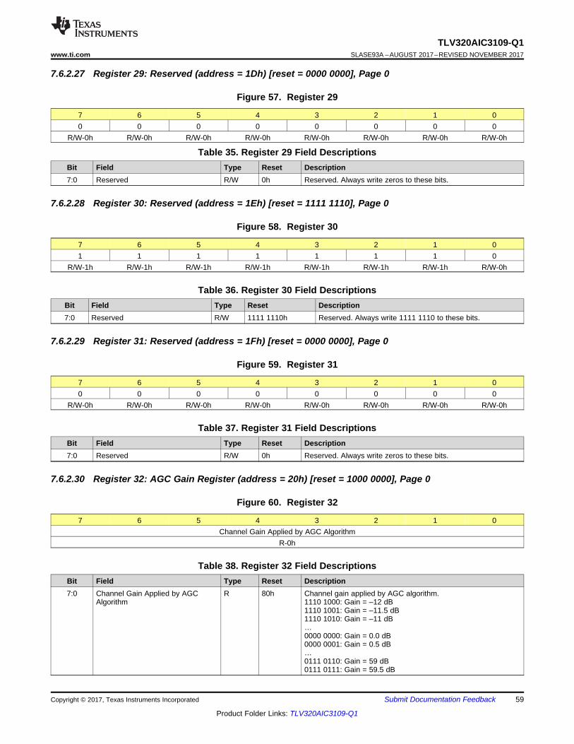
59
TLV320AIC3109-Q1www.ti.com SLASE93A –AUGUST 2017–REVISED NOVEMBER 2017
Product Folder Links: TLV320AIC3109-Q1
Submit Documentation FeedbackCopyright © 2017, Texas Instruments Incorporated
7.6.2.27 Register 29: Reserved (address = 1Dh) [reset = 0000 0000], Page 0
Figure 57. Register 29
7 6 5 4 3 2 1 00 0 0 0 0 0 0 0
R/W-0h R/W-0h R/W-0h R/W-0h R/W-0h R/W-0h R/W-0h R/W-0h
Table 35. Register 29 Field DescriptionsBit Field Type Reset Description7:0 Reserved R/W 0h Reserved. Always write zeros to these bits.
7.6.2.28 Register 30: Reserved (address = 1Eh) [reset = 1111 1110], Page 0
Figure 58. Register 30
7 6 5 4 3 2 1 01 1 1 1 1 1 1 0
R/W-1h R/W-1h R/W-1h R/W-1h R/W-1h R/W-1h R/W-1h R/W-0h
Table 36. Register 30 Field DescriptionsBit Field Type Reset Description7:0 Reserved R/W 1111 1110h Reserved. Always write 1111 1110 to these bits.
7.6.2.29 Register 31: Reserved (address = 1Fh) [reset = 0000 0000], Page 0
Figure 59. Register 31
7 6 5 4 3 2 1 00 0 0 0 0 0 0 0
R/W-0h R/W-0h R/W-0h R/W-0h R/W-0h R/W-0h R/W-0h R/W-0h
Table 37. Register 31 Field DescriptionsBit Field Type Reset Description7:0 Reserved R/W 0h Reserved. Always write zeros to these bits.
7.6.2.30 Register 32: AGC Gain Register (address = 20h) [reset = 1000 0000], Page 0
Figure 60. Register 32
7 6 5 4 3 2 1 0Channel Gain Applied by AGC Algorithm
R-0h
Table 38. Register 32 Field DescriptionsBit Field Type Reset Description7:0 Channel Gain Applied by AGC
AlgorithmR 80h Channel gain applied by AGC algorithm.
1110 1000: Gain = –12 dB1110 1001: Gain = –11.5 dB1110 1010: Gain = –11 dB…0000 0000: Gain = 0.0 dB0000 0001: Gain = 0.5 dB…0111 0110: Gain = 59 dB0111 0111: Gain = 59.5 dB
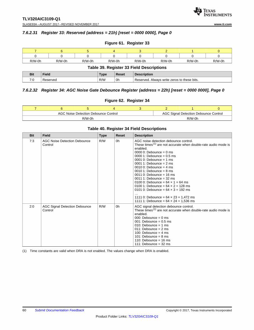
60
TLV320AIC3109-Q1SLASE93A –AUGUST 2017–REVISED NOVEMBER 2017 www.ti.com
Product Folder Links: TLV320AIC3109-Q1
Submit Documentation Feedback Copyright © 2017, Texas Instruments Incorporated
7.6.2.31 Register 33: Reserved (address = 21h) [reset = 0000 0000], Page 0
Figure 61. Register 33
7 6 5 4 3 2 1 00 0 0 0 0 0 0 0
R/W-0h R/W-0h R/W-0h R/W-0h R/W-0h R/W-0h R/W-0h R/W-0h
Table 39. Register 33 Field DescriptionsBit Field Type Reset Description7:0 Reserved R/W 0h Reserved. Always write zeros to these bits.
7.6.2.32 Register 34: AGC Noise Gate Debounce Register (address = 22h) [reset = 0000 0000], Page 0
Figure 62. Register 34
7 6 5 4 3 2 1 0AGC Noise Detection Debounce Control AGC Signal Detection Debounce Control
R/W-0h R/W-0h
(1) Time constants are valid when DRA is not enabled. The values change when DRA is enabled.
Table 40. Register 34 Field DescriptionsBit Field Type Reset Description7:3 AGC Noise Detection Debounce
ControlR/W 0h AGC noise detection debounce control.
These times (1) are not accurate when double-rate audio mode isenabled.0000 0: Debounce = 0 ms0000 1: Debounce = 0.5 ms0001 0: Debounce = 1 ms0001 1: Debounce = 2 ms0010 0: Debounce = 4 ms0010 1: Debounce = 8 ms0011 0: Debounce = 16 ms0011 1: Debounce = 32 ms0100 0: Debounce = 64 × 1 = 64 ms0100 1: Debounce = 64 × 2 = 128 ms0101 0: Debounce = 64 × 3 = 192 ms…1111 0: Debounce = 64 × 23 = 1,472 ms1111 1: Debounce = 64 × 24 = 1,536 ms
2:0 AGC Signal Detection DebounceControl
R/W 0h AGC signal detection debounce control.These times (1) are not accurate when double-rate audio mode isenabled.000: Debounce = 0 ms001: Debounce = 0.5 ms010: Debounce = 1 ms011: Debounce = 2 ms100: Debounce = 4 ms101: Debounce = 8 ms110: Debounce = 16 ms111: Debounce = 32 ms
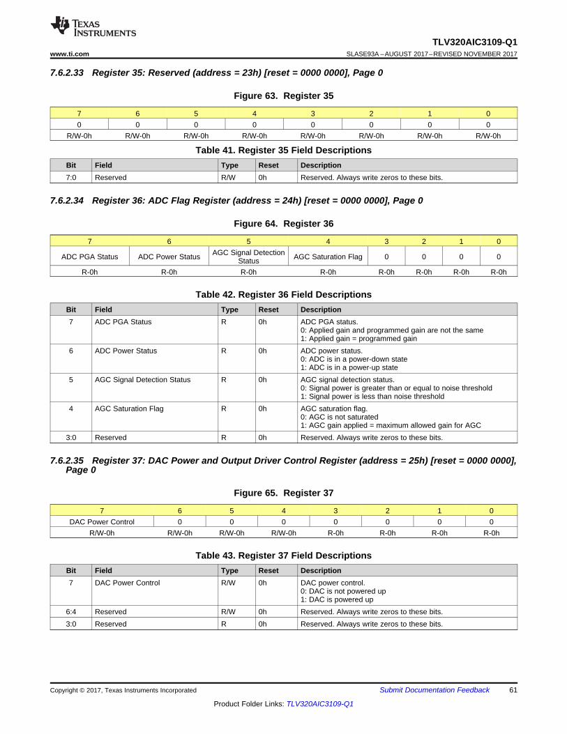
61
TLV320AIC3109-Q1www.ti.com SLASE93A –AUGUST 2017–REVISED NOVEMBER 2017
Product Folder Links: TLV320AIC3109-Q1
Submit Documentation FeedbackCopyright © 2017, Texas Instruments Incorporated
7.6.2.33 Register 35: Reserved (address = 23h) [reset = 0000 0000], Page 0
Figure 63. Register 35
7 6 5 4 3 2 1 00 0 0 0 0 0 0 0
R/W-0h R/W-0h R/W-0h R/W-0h R/W-0h R/W-0h R/W-0h R/W-0h
Table 41. Register 35 Field DescriptionsBit Field Type Reset Description7:0 Reserved R/W 0h Reserved. Always write zeros to these bits.
7.6.2.34 Register 36: ADC Flag Register (address = 24h) [reset = 0000 0000], Page 0
Figure 64. Register 36
7 6 5 4 3 2 1 0
ADC PGA Status ADC Power Status AGC Signal DetectionStatus AGC Saturation Flag 0 0 0 0
R-0h R-0h R-0h R-0h R-0h R-0h R-0h R-0h
Table 42. Register 36 Field DescriptionsBit Field Type Reset Description7 ADC PGA Status R 0h ADC PGA status.
0: Applied gain and programmed gain are not the same1: Applied gain = programmed gain
6 ADC Power Status R 0h ADC power status.0: ADC is in a power-down state1: ADC is in a power-up state
5 AGC Signal Detection Status R 0h AGC signal detection status.0: Signal power is greater than or equal to noise threshold1: Signal power is less than noise threshold
4 AGC Saturation Flag R 0h AGC saturation flag.0: AGC is not saturated1: AGC gain applied = maximum allowed gain for AGC
3:0 Reserved R 0h Reserved. Always write zeros to these bits.
7.6.2.35 Register 37: DAC Power and Output Driver Control Register (address = 25h) [reset = 0000 0000],Page 0
Figure 65. Register 37
7 6 5 4 3 2 1 0DAC Power Control 0 0 0 0 0 0 0
R/W-0h R/W-0h R/W-0h R/W-0h R-0h R-0h R-0h R-0h
Table 43. Register 37 Field DescriptionsBit Field Type Reset Description7 DAC Power Control R/W 0h DAC power control.
0: DAC is not powered up1: DAC is powered up
6:4 Reserved R/W 0h Reserved. Always write zeros to these bits.3:0 Reserved R 0h Reserved. Always write zeros to these bits.

62
TLV320AIC3109-Q1SLASE93A –AUGUST 2017–REVISED NOVEMBER 2017 www.ti.com
Product Folder Links: TLV320AIC3109-Q1
Submit Documentation Feedback Copyright © 2017, Texas Instruments Incorporated
7.6.2.36 Register 38: High-Power Output Driver Control Register (address = 26h) [reset = 0000 0000],Page 0
Figure 66. Register 38
7 6 5 4 3 2 1 0
0 0 HPCOM Output Driver ConfigurationControl
Short-Circuit ProtectionControl
Short-Circuit ProtectionMode Control 0
R-0h R-0h R/W-0h R/W-0h R/W-0h R-0h
Table 44. Register 38 Field DescriptionsBit Field Type Reset Description7:6 Reserved R 0h Reserved. Always write zeros to these register bits.5:3 HPCOM Output Driver Configuration
ControlR/W 0h HPCOM output driver configuration control.
000: HPCOM is configured as a differential of HPOUT001: HPCOM is configured as a constant VCM output010: HPCOM is configured as independent single-ended output011-111: Reserved
2 Short-Circuit Protection Control R/W 0h Short-circuit protection control.0: Short-circuit protection on all high-power output drivers isdisabled1: Short-circuit protection on all high-power output drivers isenabled
1 Short-Circuit Protection ModeControl
R/W 0h Short-circuit protection mode control.0: If short-circuit protection is enabled, the maximum current islimited to the load1: If short-circuit protection is enabled, the output driver isautomatically powered down when a short is detected
0 Reserved R 0h Reserved. Always write a zero to this bit.
7.6.2.37 Register 39: Reserved (address = 27h) [reset = 0000 0000], Page 0
Figure 67. Register 39
7 6 5 4 3 2 1 00 0 0 0 0 0 0 0
R-0h R-0h R-0h R-0h R-0h R-0h R-0h R-0h
Table 45. Register 39 Field DescriptionsBit Field Type Reset Description7:0 Reserved R 0h Reserved. Always write zeros to these bits.

63
TLV320AIC3109-Q1www.ti.com SLASE93A –AUGUST 2017–REVISED NOVEMBER 2017
Product Folder Links: TLV320AIC3109-Q1
Submit Documentation FeedbackCopyright © 2017, Texas Instruments Incorporated
7.6.2.38 Register 40: High-Power Output Stage Control Register (address = 28h) [reset = 0000 0000],Page 0
Figure 68. Register 40
7 6 5 4 3 2 1 0Output Common-Mode Voltage
Control 0 0 0 0 Output Volume Control Soft-Stepping
R/W-0h R/W-0h R/W-0h R/W-0h R/W-0h R/W-0h
Table 46. Register 40 Field DescriptionsBit Field Type Reset Description7:6 Output Common-Mode Voltage
ControlR/W 0h Output common-mode voltage control.
00: Output common-mode voltage = 1.35 V01: Output common-mode voltage = 1.5 V10: Output common-mode voltage = 1.65 V11: Output common-mode voltage = 1.8 V
5:2 Reserved R/W 0h Reserved. Always write zeros to these bits.1:0 Output Volume Control Soft-
SteppingR/W 0h Output volume control soft-stepping.
00: Output soft-stepping = one step per sample period01: Output soft-stepping = one step per two sample periods10: Output soft-stepping disabled11: Reserved; do not write this sequence to these bits
7.6.2.39 Register 41: DAC Output Switching Control Register (address = 29h) [reset = 0000 0000], Page 0
Figure 69. Register 41
7 6 5 4 3 2 1 0DAC Output Switching Control 0 0 0 0 0 0
R/W-0h R/W-0h R/W-0h R/W-0h R/W-0h R/W-0h R/W-0h
Table 47. Register 41 Field DescriptionsBit Field Type Reset Description7:6 DAC Output Switching Control R/W 0h DAC output switching control.
00: DAC output selects DAC_1 path01: DAC output selects DAC_3 path to left line output driver10, 11: Reserved. Do not write this sequence to these registerbits
5:0 Reserved R/W 0h Reserved. Always write zeros to these bits.
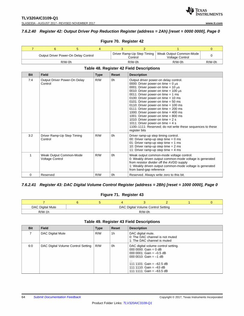
64
TLV320AIC3109-Q1SLASE93A –AUGUST 2017–REVISED NOVEMBER 2017 www.ti.com
Product Folder Links: TLV320AIC3109-Q1
Submit Documentation Feedback Copyright © 2017, Texas Instruments Incorporated
7.6.2.40 Register 42: Output Driver Pop Reduction Register (address = 2Ah) [reset = 0000 0000], Page 0
Figure 70. Register 42
7 6 5 4 3 2 1 0
Output Driver Power-On Delay Control Driver Ramp-Up Step TimingControl
Weak Output Common-ModeVoltage Control 0
R/W-0h R/W-0h R/W-0h R/W-0h
Table 48. Register 42 Field DescriptionsBit Field Type Reset Description7:4 Output Driver Power-On Delay
ControlR/W 0h Output driver power-on delay control.
0000: Driver power-on time = 0 μs0001: Driver power-on time = 10 μs0010: Driver power-on time = 100 μs0011: Driver power-on time = 1 ms0100: Driver power-on time = 10 ms0101: Driver power-on time = 50 ms0110: Driver power-on time = 100 ms0111: Driver power-on time = 200 ms1000: Driver power-on time = 400 ms1001: Driver power-on time = 800 ms1010: Driver power-on time = 2 s1011: Driver power-on time = 4 s1100–1111: Reserved; do not write these sequences to theseregister bits
3:2 Driver Ramp-Up Step TimingControl
R/W 0h Driver ramp-up step timing control.00: Driver ramp-up step time = 0 ms01: Driver ramp-up step time = 1 ms10: Driver ramp-up step time = 2 ms11: Driver ramp-up step time = 4 ms
1 Weak Output Common-ModeVoltage Control
R/W 0h Weak output common-mode voltage control.0: Weakly driven output common-mode voltage is generatedfrom resistor divider off the AVDD supply1: Weakly driven output common-mode voltage is generatedfrom band-gap reference
0 Reserved R/W 0h Reserved. Always write zero to this bit.
7.6.2.41 Register 43: DAC Digital Volume Control Register (address = 2Bh) [reset = 1000 0000], Page 0
Figure 71. Register 43
7 6 5 4 3 2 1 0DAC Digital Mute DAC Digital Volume Control Setting
R/W-1h R/W-0h
Table 49. Register 43 Field DescriptionsBit Field Type Reset Description7 DAC Digital Mute R/W 1h DAC digital mute.
0: The DAC channel is not muted1: The DAC channel is muted
6:0 DAC Digital Volume Control Setting R/W 0h DAC digital volume control setting.000 0000: Gain = 0 dB000 0001: Gain = –0.5 dB000 0010: Gain = –1 dB…111 1101: Gain = –62.5 dB111 1110: Gain = –63 dB111 1111: Gain = –63.5 dB

65
TLV320AIC3109-Q1www.ti.com SLASE93A –AUGUST 2017–REVISED NOVEMBER 2017
Product Folder Links: TLV320AIC3109-Q1
Submit Documentation FeedbackCopyright © 2017, Texas Instruments Incorporated
7.6.2.42 Register 44: Reserved (address = 2Ch) [reset = 1000 0000], Page 0
Figure 72. Register 44
7 6 5 4 3 2 1 01 0 0 0 0 0 0 0
R/W-1h R/W-0h R/W-0h R/W-0h R/W-0h R/W-0h R/W-0h R/W-0h
Table 50. Register 44 Field DescriptionsBit Field Type Reset Description7:0 Reserved R/W 1000 0000h Reserved. Always write 1000 0000 to these bits.
7.6.2.43 Registers 45–50: Reserved (address = 2Dh–32h) [reset = 0000 0000], Page 0
Figure 73. Register 45
7 6 5 4 3 2 1 00 0 0 0 0 0 0 0
R/W-0h R/W-0h R/W-0h R/W-0h R/W-0h R/W-0h R/W-0h R/W-0h
Table 51. Register 45 Field DescriptionsBit Field Type Reset Description7:0 Reserved R/W 0h Reserved. Always write zeros to these bits.
7.6.2.44 Register 51: Reserved (address = 33h) [reset = 0000 0100], Page 0
Figure 74. Register 51
7 6 5 4 3 2 1 00 0 0 0 0 1 1 0
R/W-0h R/W-0h R/W-0h R/W-0h R/W-0h R/W-1h R/W-1h R/W-0h
Table 52. Register 51 Field DescriptionsBit Field Type Reset Description7:0 Reserved R/W 0000 0100h Reserved. Always write 0000 0100 to these bits.
7.6.2.45 Registers 52–57: Reserved (address = 34h–39h) [reset = 0000 0000], Page 0
Figure 75. Register 52
7 6 5 4 3 2 1 00 0 0 0 0 0 0 0
R/W-0h R/W-0h R/W-0h R/W-0h R/W-0h R/W-0h R/W-0h R/W-0h
Table 53. Register 52 Field DescriptionsBit Field Type Reset Description7:0 Reserved R/W 0h Reserved. Always write zeros to these bits.
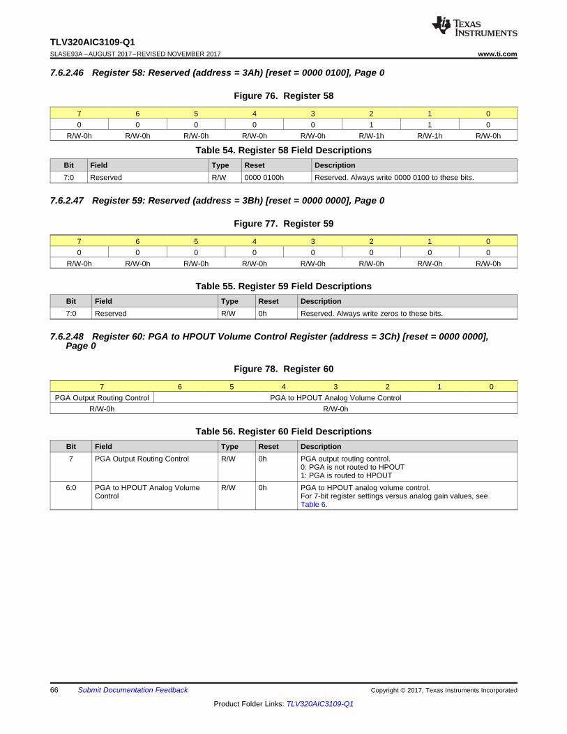
66
TLV320AIC3109-Q1SLASE93A –AUGUST 2017–REVISED NOVEMBER 2017 www.ti.com
Product Folder Links: TLV320AIC3109-Q1
Submit Documentation Feedback Copyright © 2017, Texas Instruments Incorporated
7.6.2.46 Register 58: Reserved (address = 3Ah) [reset = 0000 0100], Page 0
Figure 76. Register 58
7 6 5 4 3 2 1 00 0 0 0 0 1 1 0
R/W-0h R/W-0h R/W-0h R/W-0h R/W-0h R/W-1h R/W-1h R/W-0h
Table 54. Register 58 Field DescriptionsBit Field Type Reset Description7:0 Reserved R/W 0000 0100h Reserved. Always write 0000 0100 to these bits.
7.6.2.47 Register 59: Reserved (address = 3Bh) [reset = 0000 0000], Page 0
Figure 77. Register 59
7 6 5 4 3 2 1 00 0 0 0 0 0 0 0
R/W-0h R/W-0h R/W-0h R/W-0h R/W-0h R/W-0h R/W-0h R/W-0h
Table 55. Register 59 Field DescriptionsBit Field Type Reset Description7:0 Reserved R/W 0h Reserved. Always write zeros to these bits.
7.6.2.48 Register 60: PGA to HPOUT Volume Control Register (address = 3Ch) [reset = 0000 0000],Page 0
Figure 78. Register 60
7 6 5 4 3 2 1 0PGA Output Routing Control PGA to HPOUT Analog Volume Control
R/W-0h R/W-0h
Table 56. Register 60 Field DescriptionsBit Field Type Reset Description7 PGA Output Routing Control R/W 0h PGA output routing control.
0: PGA is not routed to HPOUT1: PGA is routed to HPOUT
6:0 PGA to HPOUT Analog VolumeControl
R/W 0h PGA to HPOUT analog volume control.For 7-bit register settings versus analog gain values, seeTable 6.

67
TLV320AIC3109-Q1www.ti.com SLASE93A –AUGUST 2017–REVISED NOVEMBER 2017
Product Folder Links: TLV320AIC3109-Q1
Submit Documentation FeedbackCopyright © 2017, Texas Instruments Incorporated
7.6.2.49 Register 61: DAC_1 to HPOUT Volume Control Register (address = 3Dh) [reset = 0000 0000],Page 0
Figure 79. Register 61
7 6 5 4 3 2 1 0DAC_1 Output Routing
Control DAC_1 to HPOUT Analog Volume Control
R/W-0h R/W-0h
Table 57. Register 61 Field DescriptionsBit Field Type Reset Description7 DAC_1 Output Routing Control R/W 0h DAC_1 output routing control.
0: DAC_1 is not routed to HPOUT1: DAC_1 is routed to HPOUT
6:0 DAC_1 to HPOUT Analog VolumeControl
R/W 0h DAC_1 to HPOUT analog volume control.For 7-bit register settings versus analog gain values, seeTable 6.
7.6.2.50 Register 62: Reserved Register (address = 3Eh) [reset = 0000 0000], Page 0
Figure 80. Register 62
7 6 5 4 3 2 1 00 0 0 0 0 0 0 0
R/W-0h R/W-0h R/W-0h R/W-0h R/W-0h R/W-0h R/W-0h R/W-0h
Table 58. Register 62 Field DescriptionsBit Field Type Reset Description7:0 Reserved R/W 0h Reserved. Always write zeros to these bits.
7.6.2.51 Register 63: PGA_AUX to HPOUT Volume Control Register (address = 3Fh) [reset = 0000 0000],Page 0
Figure 81. Register 63
7 6 5 4 3 2 1 0PGA_AUX Output Routing
Control PGA_AUX to HPOUT Analog Volume Control
R/W-0h R/W-0h
Table 59. Register 63 Field DescriptionsBit Field Type Reset Description7 PGA_AUX Output Routing Control R/W 0h PGA_AUX output routing control.
0: PGA_AUX is not routed to HPOUT1: PGA_AUX is routed to HPOUT
6:0 PGA_AUX to HPOUT AnalogVolume Control
R/W 0h PGA_AUX to HPOUT analog volume control.For 7-bit register settings versus analog gain values, seeTable 6.

68
TLV320AIC3109-Q1SLASE93A –AUGUST 2017–REVISED NOVEMBER 2017 www.ti.com
Product Folder Links: TLV320AIC3109-Q1
Submit Documentation Feedback Copyright © 2017, Texas Instruments Incorporated
7.6.2.52 Register 64: Reserved (address = 40h) [reset = 0000 0000], Page 0
Figure 82. Register 64
7 6 5 4 3 2 1 00 0 0 0 0 0 0 0
R/W-0h R/W-0h R/W-0h R/W-0h R/W-0h R/W-0h R/W-0h R/W-0h
Table 60. Register 64 Field DescriptionsBit Field Type Reset Description7:0 Reserved RW 0h Reserved. Always write zeros to these bits.
7.6.2.53 Register 65: HPOUT Output Level Control Register (address = 41h) [reset = 0000 0100], Page 0
Figure 83. Register 65
7 6 5 4 3 2 1 0
HPOUT Output Level Control HPOUT Mute HPOUT Power-DownDrive Control
HPOUT VolumeControl Status
HPOUT PowerControl
R/W-0h R/W-0h R/W-1h R-0h R/W-0h
Table 61. Register 65 Field DescriptionsBit Field Type Reset Description7:4 HPOUT Output Level Control R/W 0h HPOUT output level control.
0000: Output level control = 0 dB0001: Output level control = 1 dB0010: Output level control = 2 dB...1000: Output level control = 8 dB1001: Output level control = 9 dB1010–1111: Reserved; do not write these sequences to theseregister bits
3 HPOUT Mute R/W 0h HPOUT mute.0: HPOUT is muted1: HPOUT is not muted.
2 HPOUT Power-Down Drive Control R/W 1h HPOUT power-down drive control.0: HPOUT is weakly driven to a common mode when powereddown1: HPOUT is high-impedance when powered down
1 HPOUT Volume Control Status R 0h HPOUT volume control status.0: All programmed gains to HPOUT are applied1: Not all programmed gains to HPOUT are applied yet
0 HPOUT Power Control R/W 0h HPOUT power control.0: HPOUT is not fully powered up1: HPOUT is fully powered up
7.6.2.54 Register 66: Reserved (address = 42h) [reset = 0000 0000], Page 0
Figure 84. Register 66
7 6 5 4 3 2 1 00 0 0 0 0 0 0 0
R/W-0h R/W-0h R/W-0h R/W-0h R/W-0h R/W-0h R/W-0h R/W-0h
Table 62. Register 66 Field DescriptionsBit Field Type Reset Description7:0 Reserved R/W 0h Reserved. Always write zeros to these bits.
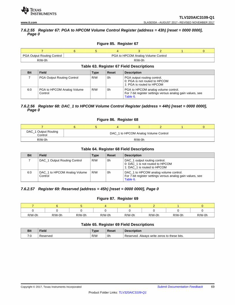
69
TLV320AIC3109-Q1www.ti.com SLASE93A –AUGUST 2017–REVISED NOVEMBER 2017
Product Folder Links: TLV320AIC3109-Q1
Submit Documentation FeedbackCopyright © 2017, Texas Instruments Incorporated
7.6.2.55 Register 67: PGA to HPCOM Volume Control Register (address = 43h) [reset = 0000 0000],Page 0
Figure 85. Register 67
7 6 5 4 3 2 1 0PGA Output Routing Control PGA to HPCOM Analog Volume Control
R/W-0h R/W-0h
Table 63. Register 67 Field DescriptionsBit Field Type Reset Description7 PGA Output Routing Control R/W 0h PGA output routing control.
0: PGA is not routed to HPCOM1: PGA is routed to HPCOM
6:0 PGA to HPCOM Analog VolumeControl
R/W 0h PGA to HPCOM analog volume control.For 7-bit register settings versus analog gain values, seeTable 6.
7.6.2.56 Register 68: DAC_1 to HPCOM Volume Control Register (address = 44h) [reset = 0000 0000],Page 0
Figure 86. Register 68
7 6 5 4 3 2 1 0DAC_1 Output Routing
Control DAC_1 to HPCOM Analog Volume Control
R/W-0h R/W-0h
Table 64. Register 68 Field DescriptionsBit Field Type Reset Description7 DAC_1 Output Routing Control R/W 0h DAC_1 output routing control.
0: DAC_1 is not routed to HPCOM1: DAC_1 is routed to HPCOM
6:0 DAC_1 to HPCOM Analog VolumeControl
R/W 0h DAC_1 to HPCOM analog volume control.For 7-bit register settings versus analog gain values, seeTable 6.
7.6.2.57 Register 69: Reserved (address = 45h) [reset = 0000 0000], Page 0
Figure 87. Register 69
7 6 5 4 3 2 1 00 0 0 0 0 0 0 0
R/W-0h R/W-0h R/W-0h R/W-0h R/W-0h R/W-0h R/W-0h R/W-0h
Table 65. Register 69 Field DescriptionsBit Field Type Reset Description7:0 Reserved R/W 0h Reserved. Always write zeros to these bits.

70
TLV320AIC3109-Q1SLASE93A –AUGUST 2017–REVISED NOVEMBER 2017 www.ti.com
Product Folder Links: TLV320AIC3109-Q1
Submit Documentation Feedback Copyright © 2017, Texas Instruments Incorporated
7.6.2.58 Register 70: PGA_AUX to HPCOM Volume Control Register (address = 46h) [reset = 0000 0000],Page 0
Figure 88. Register 70
7 6 5 4 3 2 1 0PGA_AUX Output Routing
Control PGA_AUX to HPCOM Analog Volume Control
R/W-0h R/W-0h
Table 66. Register 70 Field DescriptionsBit Field Type Reset Description7 PGA_AUX Output Routing Control R/W 0h PGA_AUX output routing control.
0: PGA_AUX is not routed to HPCOM1: PGA_AUX is routed to HPCOM
6:0 PGA_AUX to HPCOM AnalogVolume Control
R/W 0h PGA_AUX to HPCOM analog volume control.For 7-bit register settings versus analog gain values, seeTable 6.
7.6.2.59 Register 71: Reserved (address = 47h) [reset = 0000 0000], Page 0
Figure 89. Register 71
7 6 5 4 3 2 1 00 0 0 0 0 0 0 0
R/W-0h R/W-0h R/W-0h R/W-0h R/W-0h R/W-0h R/W-0h R/W-0h
Table 67. Register 71 Field DescriptionsBit Field Type Reset Description7:0 Reserved R/W 0h Reserved. Always write zeros to these bits.
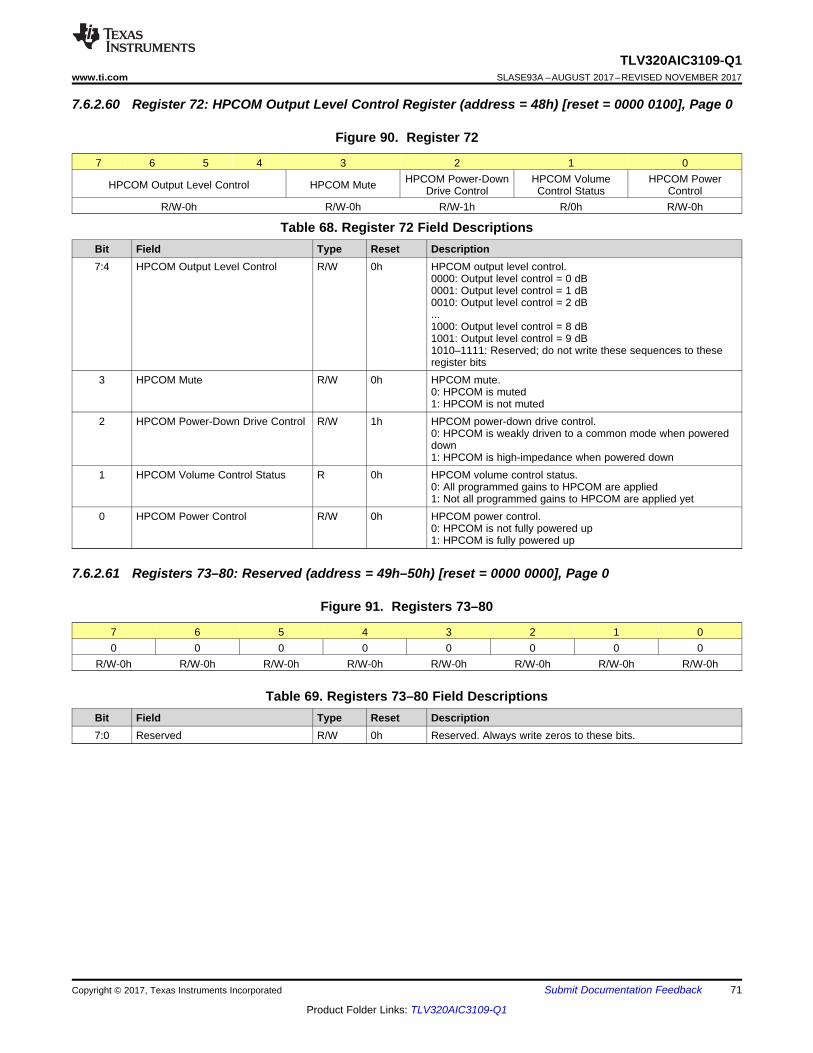
71
TLV320AIC3109-Q1www.ti.com SLASE93A –AUGUST 2017–REVISED NOVEMBER 2017
Product Folder Links: TLV320AIC3109-Q1
Submit Documentation FeedbackCopyright © 2017, Texas Instruments Incorporated
7.6.2.60 Register 72: HPCOM Output Level Control Register (address = 48h) [reset = 0000 0100], Page 0
Figure 90. Register 72
7 6 5 4 3 2 1 0
HPCOM Output Level Control HPCOM Mute HPCOM Power-DownDrive Control
HPCOM VolumeControl Status
HPCOM PowerControl
R/W-0h R/W-0h R/W-1h R/0h R/W-0h
Table 68. Register 72 Field DescriptionsBit Field Type Reset Description7:4 HPCOM Output Level Control R/W 0h HPCOM output level control.
0000: Output level control = 0 dB0001: Output level control = 1 dB0010: Output level control = 2 dB...1000: Output level control = 8 dB1001: Output level control = 9 dB1010–1111: Reserved; do not write these sequences to theseregister bits
3 HPCOM Mute R/W 0h HPCOM mute.0: HPCOM is muted1: HPCOM is not muted
2 HPCOM Power-Down Drive Control R/W 1h HPCOM power-down drive control.0: HPCOM is weakly driven to a common mode when powereddown1: HPCOM is high-impedance when powered down
1 HPCOM Volume Control Status R 0h HPCOM volume control status.0: All programmed gains to HPCOM are applied1: Not all programmed gains to HPCOM are applied yet
0 HPCOM Power Control R/W 0h HPCOM power control.0: HPCOM is not fully powered up1: HPCOM is fully powered up
7.6.2.61 Registers 73–80: Reserved (address = 49h–50h) [reset = 0000 0000], Page 0
Figure 91. Registers 73–80
7 6 5 4 3 2 1 00 0 0 0 0 0 0 0
R/W-0h R/W-0h R/W-0h R/W-0h R/W-0h R/W-0h R/W-0h R/W-0h
Table 69. Registers 73–80 Field DescriptionsBit Field Type Reset Description7:0 Reserved R/W 0h Reserved. Always write zeros to these bits.
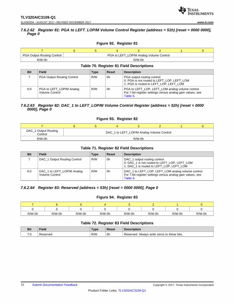
72
TLV320AIC3109-Q1SLASE93A –AUGUST 2017–REVISED NOVEMBER 2017 www.ti.com
Product Folder Links: TLV320AIC3109-Q1
Submit Documentation Feedback Copyright © 2017, Texas Instruments Incorporated
7.6.2.62 Register 81: PGA to LEFT_LOP/M Volume Control Register (address = 51h) [reset = 0000 0000],Page 0
Figure 92. Register 81
7 6 5 4 3 2 1 0PGA Output Routing Control PGA to LEFT_LOP/M Analog Volume Control
R/W-0h R/W-0h
Table 70. Register 81 Field DescriptionsBit Field Type Reset Description7 PGA Output Routing Control R/W 0h PGA output routing control.
0: PGA is not routed to LEFT_LOP, LEFT_LOM1: PGA is routed to LEFT_LOP, LEFT_LOM
6:0 PGA to LEFT_LOP/M AnalogVolume Control
R/W 0h PGA to LEFT_LOP, LEFT_LOM analog volume control.For 7-bit register settings versus analog gain values, seeTable 6.
7.6.2.63 Register 82: DAC_1 to LEFT_LOP/M Volume Control Register (address = 52h) [reset = 00000000], Page 0
Figure 93. Register 82
7 6 5 4 3 2 1 0DAC_1 Output Routing
Control DAC_1 to LEFT_LOP/M Analog Volume Control
R/W-0h R/W-0h
Table 71. Register 82 Field DescriptionsBit Field Type Reset Description7 DAC_1 Output Routing Control R/W 0h DAC_1 output routing control.
0: DAC_1 is not routed to LEFT_LOP, LEFT_LOM1: DAC_1 is routed to LEFT_LOP, LEFT_LOM
6:0 DAC_1 to LEFT_LOP/M AnalogVolume Control
R/W 0h DAC_1 to LEFT_LOP, LEFT_LOM analog volume control.For 7-bit register settings versus analog gain values, seeTable 6.
7.6.2.64 Register 83: Reserved (address = 53h) [reset = 0000 0000], Page 0
Figure 94. Register 83
7 6 5 4 3 2 1 00 0 0 0 0 0 0 0
R/W-0h R/W-0h R/W-0h R/W-0h R/W-0h R/W-0h R/W-0h R/W-0h
Table 72. Register 83 Field DescriptionsBit Field Type Reset Description7:0 Reserved R/W 0h Reserved. Always write zeros to these bits.
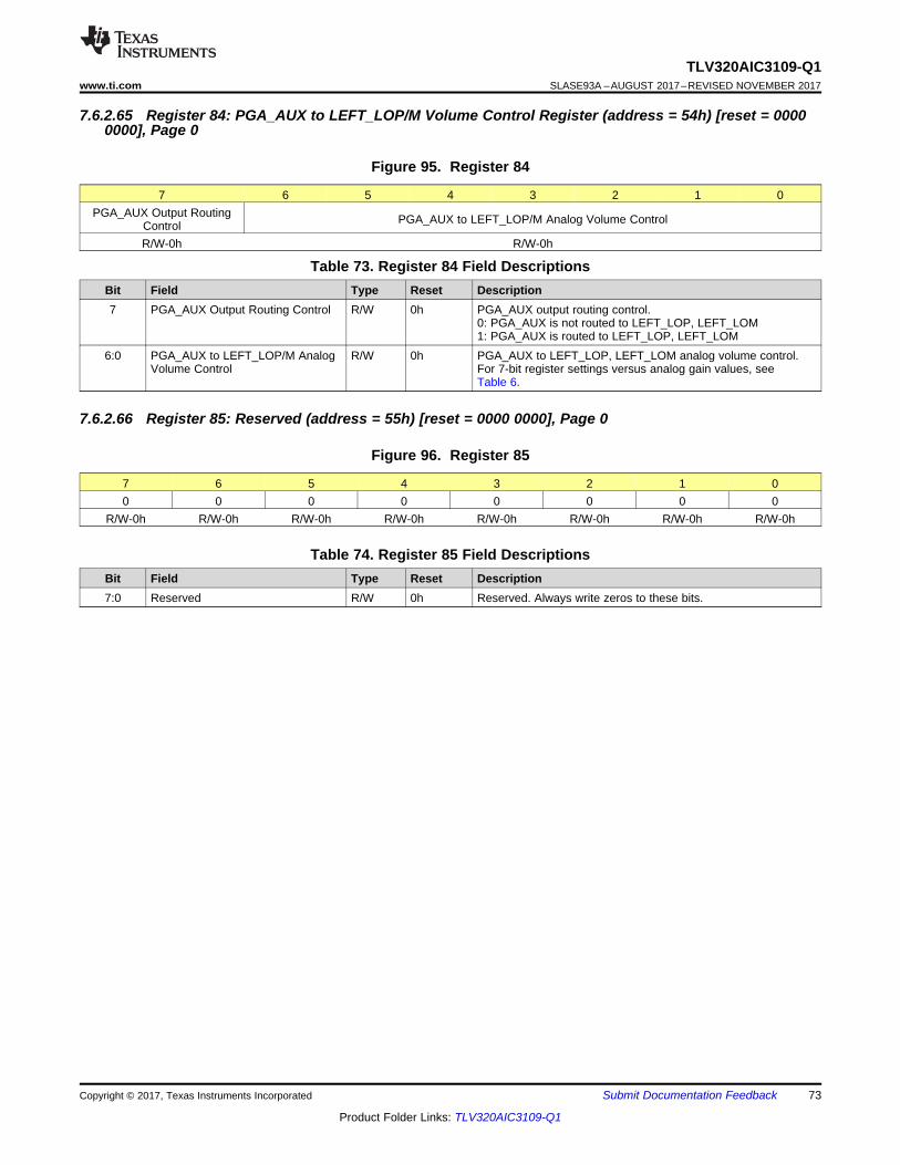
73
TLV320AIC3109-Q1www.ti.com SLASE93A –AUGUST 2017–REVISED NOVEMBER 2017
Product Folder Links: TLV320AIC3109-Q1
Submit Documentation FeedbackCopyright © 2017, Texas Instruments Incorporated
7.6.2.65 Register 84: PGA_AUX to LEFT_LOP/M Volume Control Register (address = 54h) [reset = 00000000], Page 0
Figure 95. Register 84
7 6 5 4 3 2 1 0PGA_AUX Output Routing
Control PGA_AUX to LEFT_LOP/M Analog Volume Control
R/W-0h R/W-0h
Table 73. Register 84 Field DescriptionsBit Field Type Reset Description7 PGA_AUX Output Routing Control R/W 0h PGA_AUX output routing control.
0: PGA_AUX is not routed to LEFT_LOP, LEFT_LOM1: PGA_AUX is routed to LEFT_LOP, LEFT_LOM
6:0 PGA_AUX to LEFT_LOP/M AnalogVolume Control
R/W 0h PGA_AUX to LEFT_LOP, LEFT_LOM analog volume control.For 7-bit register settings versus analog gain values, seeTable 6.
7.6.2.66 Register 85: Reserved (address = 55h) [reset = 0000 0000], Page 0
Figure 96. Register 85
7 6 5 4 3 2 1 00 0 0 0 0 0 0 0
R/W-0h R/W-0h R/W-0h R/W-0h R/W-0h R/W-0h R/W-0h R/W-0h
Table 74. Register 85 Field DescriptionsBit Field Type Reset Description7:0 Reserved R/W 0h Reserved. Always write zeros to these bits.

74
TLV320AIC3109-Q1SLASE93A –AUGUST 2017–REVISED NOVEMBER 2017 www.ti.com
Product Folder Links: TLV320AIC3109-Q1
Submit Documentation Feedback Copyright © 2017, Texas Instruments Incorporated
7.6.2.67 Register 86: LEFT_LOP/M Output Level Control Register (address = 56h) [reset = 0000 0000],Page 0
Figure 97. Register 86
7 6 5 4 3 2 1 0
LEFT_LOP/M Output Level Control LEFT_LOP/M Mute 0 LEFT_LOP/M VolumeControl Status
LEFT_LOP/M PowerStatus
R/W-0h R/W-0h R-0h R-0h R-0h
Table 75. Register 86 Field DescriptionsBit Field Type Reset Description7:4 LEFT_LOP/M Output Level Control R/W 0h LEFT_LOP, LEFT_LOM output level control.
0000: Output level control = 0 dB0001: Output level control = 1 dB0010: Output level control = 2 dB...1000: Output level control = 8 dB1001: Output level control = 9 dB1010–1111: Reserved; do not write these sequences to theseregister bits
3 LEFT_LOP/M Mute R/W 0h LEFT_LOP, LEFT_LOM mute.0: LEFT_LOP, LEFT_LOM are muted1: LEFT_LOP, LEFT_LOM are not muted
2 Reserved R 0h Reserved. Always write zero to this bit.1 LEFT_LOP/M Volume Control
StatusR 0h LEFT_LOP, LEFT_LOM volume control status.
0: All programmed gains to LEFT_LOP, LEFT_LOM are applied1: Not all programmed gains to LEFT_LOP, LEFT_LOM areapplied yet
0 LEFT_LOP/M Power Status R 0h LEFT_LOP, LEFT_LOM power status.0: LEFT_LOP, LEFT_LOM is not fully powered up1: LEFT_LOP, LEFT_LOM is fully powered up
7.6.2.68 Register 87: Reserved (address = 57h) [reset = 0000 0000], Page 0
Figure 98. Register 87
7 6 5 4 3 2 1 00 0 0 0 0 0 0 0
R/W-0h R/W-0h R/W-0h R/W-0h R/W-0h R/W-0h R/W-0h R/W-0h
Table 76. Register 87 Field DescriptionsBit Field Type Reset Description7:0 Reserved R/W 0h Reserved. Always write zeros to these bits.
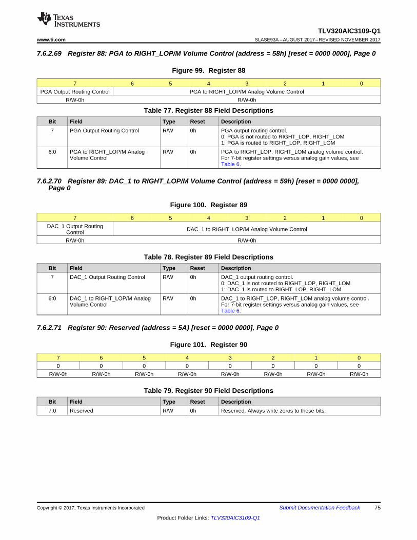
75
TLV320AIC3109-Q1www.ti.com SLASE93A –AUGUST 2017–REVISED NOVEMBER 2017
Product Folder Links: TLV320AIC3109-Q1
Submit Documentation FeedbackCopyright © 2017, Texas Instruments Incorporated
7.6.2.69 Register 88: PGA to RIGHT_LOP/M Volume Control (address = 58h) [reset = 0000 0000], Page 0
Figure 99. Register 88
7 6 5 4 3 2 1 0PGA Output Routing Control PGA to RIGHT_LOP/M Analog Volume Control
R/W-0h R/W-0h
Table 77. Register 88 Field DescriptionsBit Field Type Reset Description7 PGA Output Routing Control R/W 0h PGA output routing control.
0: PGA is not routed to RIGHT_LOP, RIGHT_LOM1: PGA is routed to RIGHT_LOP, RIGHT_LOM
6:0 PGA to RIGHT_LOP/M AnalogVolume Control
R/W 0h PGA to RIGHT_LOP, RIGHT_LOM analog volume control.For 7-bit register settings versus analog gain values, seeTable 6.
7.6.2.70 Register 89: DAC_1 to RIGHT_LOP/M Volume Control (address = 59h) [reset = 0000 0000],Page 0
Figure 100. Register 89
7 6 5 4 3 2 1 0DAC_1 Output Routing
Control DAC_1 to RIGHT_LOP/M Analog Volume Control
R/W-0h R/W-0h
Table 78. Register 89 Field DescriptionsBit Field Type Reset Description7 DAC_1 Output Routing Control R/W 0h DAC_1 output routing control.
0: DAC_1 is not routed to RIGHT_LOP, RIGHT_LOM1: DAC_1 is routed to RIGHT_LOP, RIGHT_LOM
6:0 DAC_1 to RIGHT_LOP/M AnalogVolume Control
R/W 0h DAC_1 to RIGHT_LOP, RIGHT_LOM analog volume control.For 7-bit register settings versus analog gain values, seeTable 6.
7.6.2.71 Register 90: Reserved (address = 5A) [reset = 0000 0000], Page 0
Figure 101. Register 90
7 6 5 4 3 2 1 00 0 0 0 0 0 0 0
R/W-0h R/W-0h R/W-0h R/W-0h R/W-0h R/W-0h R/W-0h R/W-0h
Table 79. Register 90 Field DescriptionsBit Field Type Reset Description7:0 Reserved R/W 0h Reserved. Always write zeros to these bits.
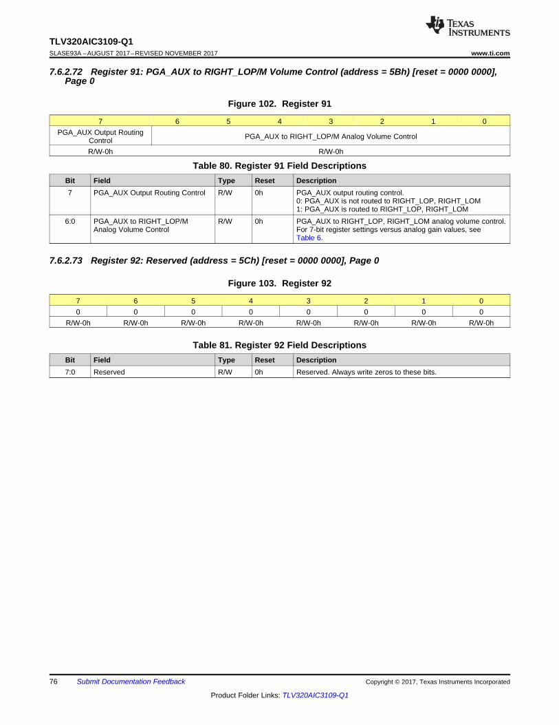
76
TLV320AIC3109-Q1SLASE93A –AUGUST 2017–REVISED NOVEMBER 2017 www.ti.com
Product Folder Links: TLV320AIC3109-Q1
Submit Documentation Feedback Copyright © 2017, Texas Instruments Incorporated
7.6.2.72 Register 91: PGA_AUX to RIGHT_LOP/M Volume Control (address = 5Bh) [reset = 0000 0000],Page 0
Figure 102. Register 91
7 6 5 4 3 2 1 0PGA_AUX Output Routing
Control PGA_AUX to RIGHT_LOP/M Analog Volume Control
R/W-0h R/W-0h
Table 80. Register 91 Field DescriptionsBit Field Type Reset Description7 PGA_AUX Output Routing Control R/W 0h PGA_AUX output routing control.
0: PGA_AUX is not routed to RIGHT_LOP, RIGHT_LOM1: PGA_AUX is routed to RIGHT_LOP, RIGHT_LOM
6:0 PGA_AUX to RIGHT_LOP/MAnalog Volume Control
R/W 0h PGA_AUX to RIGHT_LOP, RIGHT_LOM analog volume control.For 7-bit register settings versus analog gain values, seeTable 6.
7.6.2.73 Register 92: Reserved (address = 5Ch) [reset = 0000 0000], Page 0
Figure 103. Register 92
7 6 5 4 3 2 1 00 0 0 0 0 0 0 0
R/W-0h R/W-0h R/W-0h R/W-0h R/W-0h R/W-0h R/W-0h R/W-0h
Table 81. Register 92 Field DescriptionsBit Field Type Reset Description7:0 Reserved R/W 0h Reserved. Always write zeros to these bits.
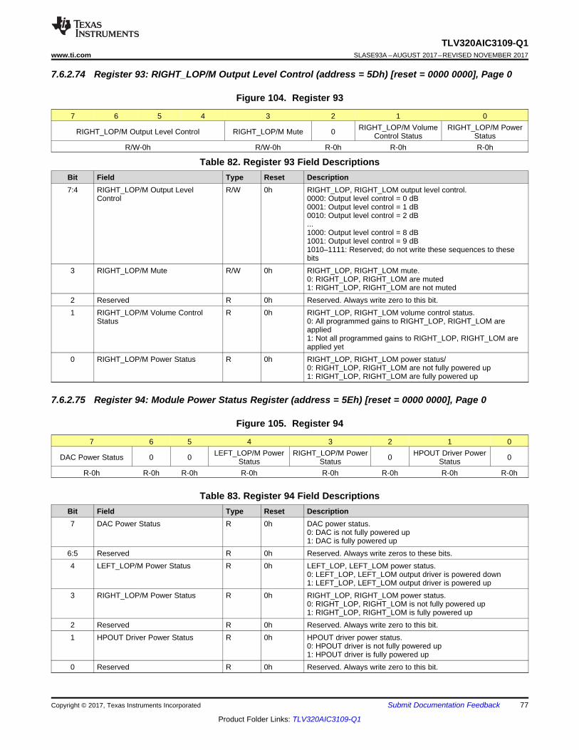
77
TLV320AIC3109-Q1www.ti.com SLASE93A –AUGUST 2017–REVISED NOVEMBER 2017
Product Folder Links: TLV320AIC3109-Q1
Submit Documentation FeedbackCopyright © 2017, Texas Instruments Incorporated
7.6.2.74 Register 93: RIGHT_LOP/M Output Level Control (address = 5Dh) [reset = 0000 0000], Page 0
Figure 104. Register 93
7 6 5 4 3 2 1 0
RIGHT_LOP/M Output Level Control RIGHT_LOP/M Mute 0 RIGHT_LOP/M VolumeControl Status
RIGHT_LOP/M PowerStatus
R/W-0h R/W-0h R-0h R-0h R-0h
Table 82. Register 93 Field DescriptionsBit Field Type Reset Description7:4 RIGHT_LOP/M Output Level
ControlR/W 0h RIGHT_LOP, RIGHT_LOM output level control.
0000: Output level control = 0 dB0001: Output level control = 1 dB0010: Output level control = 2 dB...1000: Output level control = 8 dB1001: Output level control = 9 dB1010–1111: Reserved; do not write these sequences to thesebits
3 RIGHT_LOP/M Mute R/W 0h RIGHT_LOP, RIGHT_LOM mute.0: RIGHT_LOP, RIGHT_LOM are muted1: RIGHT_LOP, RIGHT_LOM are not muted
2 Reserved R 0h Reserved. Always write zero to this bit.1 RIGHT_LOP/M Volume Control
StatusR 0h RIGHT_LOP, RIGHT_LOM volume control status.
0: All programmed gains to RIGHT_LOP, RIGHT_LOM areapplied1: Not all programmed gains to RIGHT_LOP, RIGHT_LOM areapplied yet
0 RIGHT_LOP/M Power Status R 0h RIGHT_LOP, RIGHT_LOM power status/0: RIGHT_LOP, RIGHT_LOM are not fully powered up1: RIGHT_LOP, RIGHT_LOM are fully powered up
7.6.2.75 Register 94: Module Power Status Register (address = 5Eh) [reset = 0000 0000], Page 0
Figure 105. Register 94
7 6 5 4 3 2 1 0
DAC Power Status 0 0 LEFT_LOP/M PowerStatus
RIGHT_LOP/M PowerStatus 0 HPOUT Driver Power
Status 0
R-0h R-0h R-0h R-0h R-0h R-0h R-0h R-0h
Table 83. Register 94 Field DescriptionsBit Field Type Reset Description7 DAC Power Status R 0h DAC power status.
0: DAC is not fully powered up1: DAC is fully powered up
6:5 Reserved R 0h Reserved. Always write zeros to these bits.4 LEFT_LOP/M Power Status R 0h LEFT_LOP, LEFT_LOM power status.
0: LEFT_LOP, LEFT_LOM output driver is powered down1: LEFT_LOP, LEFT_LOM output driver is powered up
3 RIGHT_LOP/M Power Status R 0h RIGHT_LOP, RIGHT_LOM power status.0: RIGHT_LOP, RIGHT_LOM is not fully powered up1: RIGHT_LOP, RIGHT_LOM is fully powered up
2 Reserved R 0h Reserved. Always write zero to this bit.1 HPOUT Driver Power Status R 0h HPOUT driver power status.
0: HPOUT driver is not fully powered up1: HPOUT driver is fully powered up
0 Reserved R 0h Reserved. Always write zero to this bit.
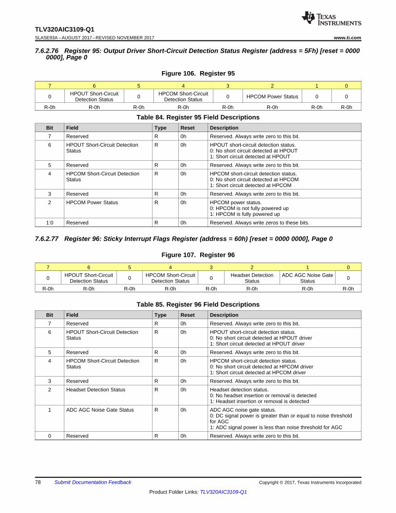
78
TLV320AIC3109-Q1SLASE93A –AUGUST 2017–REVISED NOVEMBER 2017 www.ti.com
Product Folder Links: TLV320AIC3109-Q1
Submit Documentation Feedback Copyright © 2017, Texas Instruments Incorporated
7.6.2.76 Register 95: Output Driver Short-Circuit Detection Status Register (address = 5Fh) [reset = 00000000], Page 0
Figure 106. Register 95
7 6 5 4 3 2 1 0
0 HPOUT Short-CircuitDetection Status 0 HPCOM Short-Circuit
Detection Status 0 HPCOM Power Status 0 0
R-0h R-0h R-0h R-0h R-0h R-0h R-0h R-0h
Table 84. Register 95 Field DescriptionsBit Field Type Reset Description7 Reserved R 0h Reserved. Always write zero to this bit.6 HPOUT Short-Circuit Detection
StatusR 0h HPOUT short-circuit detection status.
0: No short circuit detected at HPOUT1: Short circuit detected at HPOUT
5 Reserved R 0h Reserved. Always write zero to this bit.4 HPCOM Short-Circuit Detection
StatusR 0h HPCOM short-circuit detection status.
0: No short circuit detected at HPCOM1: Short circuit detected at HPCOM
3 Reserved R 0h Reserved. Always write zero to this bit.2 HPCOM Power Status R 0h HPCOM power status.
0: HPCOM is not fully powered up1: HPCOM is fully powered up
1:0 Reserved R 0h Reserved. Always write zeros to these bits.
7.6.2.77 Register 96: Sticky Interrupt Flags Register (address = 60h) [reset = 0000 0000], Page 0
Figure 107. Register 96
7 6 5 4 3 2 1 0
0 HPOUT Short-CircuitDetection Status 0 HPCOM Short-Circuit
Detection Status 0 Headset DetectionStatus
ADC AGC Noise GateStatus 0
R-0h R-0h R-0h R-0h R-0h R-0h R-0h R-0h
Table 85. Register 96 Field DescriptionsBit Field Type Reset Description7 Reserved R 0h Reserved. Always write zero to this bit.6 HPOUT Short-Circuit Detection
StatusR 0h HPOUT short-circuit detection status.
0: No short circuit detected at HPOUT driver1: Short circuit detected at HPOUT driver
5 Reserved R 0h Reserved. Always write zero to this bit.4 HPCOM Short-Circuit Detection
StatusR 0h HPCOM short-circuit detection status.
0: No short circuit detected at HPCOM driver1: Short circuit detected at HPCOM driver
3 Reserved R 0h Reserved. Always write zero to this bit.2 Headset Detection Status R 0h Headset detection status.
0: No headset insertion or removal is detected1: Headset insertion or removal is detected
1 ADC AGC Noise Gate Status R 0h ADC AGC noise gate status.0: DC signal power is greater than or equal to noise thresholdfor AGC1: ADC signal power is less than noise threshold for AGC
0 Reserved R 0h Reserved. Always write zero to this bit.

79
TLV320AIC3109-Q1www.ti.com SLASE93A –AUGUST 2017–REVISED NOVEMBER 2017
Product Folder Links: TLV320AIC3109-Q1
Submit Documentation FeedbackCopyright © 2017, Texas Instruments Incorporated
7.6.2.78 Register 97: Real-Time Interrupt Flags Register (address = 61h) [reset = 0000 0000], Page 0
Figure 108. Register 97
7 6 5 4 3 2 1 0
0 HPOUT Short-CircuitDetection Status 0 HPCOM Short-Circuit
Detection Status 0 Headset DetectionStatus
ADC AGC Noise GateStatus 0
R-0h R-0h R-0h R-0h R-0h R-0h R-0h R-0h
Table 86. Register 97 Field DescriptionsBit Field Type Reset Description7 Reserved R 0h Reserved. Always write zero to this bit.6 HPOUT Short-Circuit Detection
StatusR 0h HPOUT short-circuit detection status.
0: No short circuit detected at HPOUT driver1: Short circuit detected at HPOUT driver
5 Reserved R 0h Reserved. Always write zero to this bit.4 HPCOM Short-Circuit Detection
StatusR 0h HPCOM short-circuit detection status.
0: No short circuit detected at HPCOM driver1: Short circuit detected at HPCOM driver
3 Reserved R 0h Reserved. Always write zero to this bit.2 Headset Detection Status R 0h Headset Detection Status
0: No headset insertion/removal is detected.1: Headset insertion/removal is detected.
1 ADC AGC Noise Gate Status R 0h ADC AGC Noise Gate Status0: ADC signal power is greater than noise threshold for lAGC.1: ADC signal power lower than noise threshold for AGC.
0 Reserved R 0h Reserved. Always write zero to this bit.
7.6.2.79 Registers 98–100: Reserved (address = 62h–64h) [reset = 0000 0000], Page 0
Figure 109. Registers 98–100
7 6 5 4 3 2 1 00 0 0 0 0 0 0 0
R-0h R-0h R-0h R-0h R-0h R-0h R-0h R-0h
Table 87. Registers 98–100 Field DescriptionsBit Field Type Reset Description7:0 Reserved R 0h Reserved. Always write zeros to these bits.
7.6.2.80 Register 101: Clock Register (address = 65h) [reset = 0000 0000], Page 0
Figure 110. Register 101
7 6 5 4 3 2 1 0
0 0 0 0 0 0 0 CODEC_CLKIN SourceSelection
R-0h R-0h R-0h R-0h R-0h R-0h R-0h R/W-0h
Table 88. Register 101 Field DescriptionsBit Field Type Reset Description7:1 Reserved R 0h Reserved. Always write zeros to these bits.0 CODEC_CLKIN Source Selection R/W 0h CODEC_CLKIN source selection.
0: CODEC_CLKIN uses PLLDIV_OUT1: CODEC_CLKIN uses CLKDIV_OUT
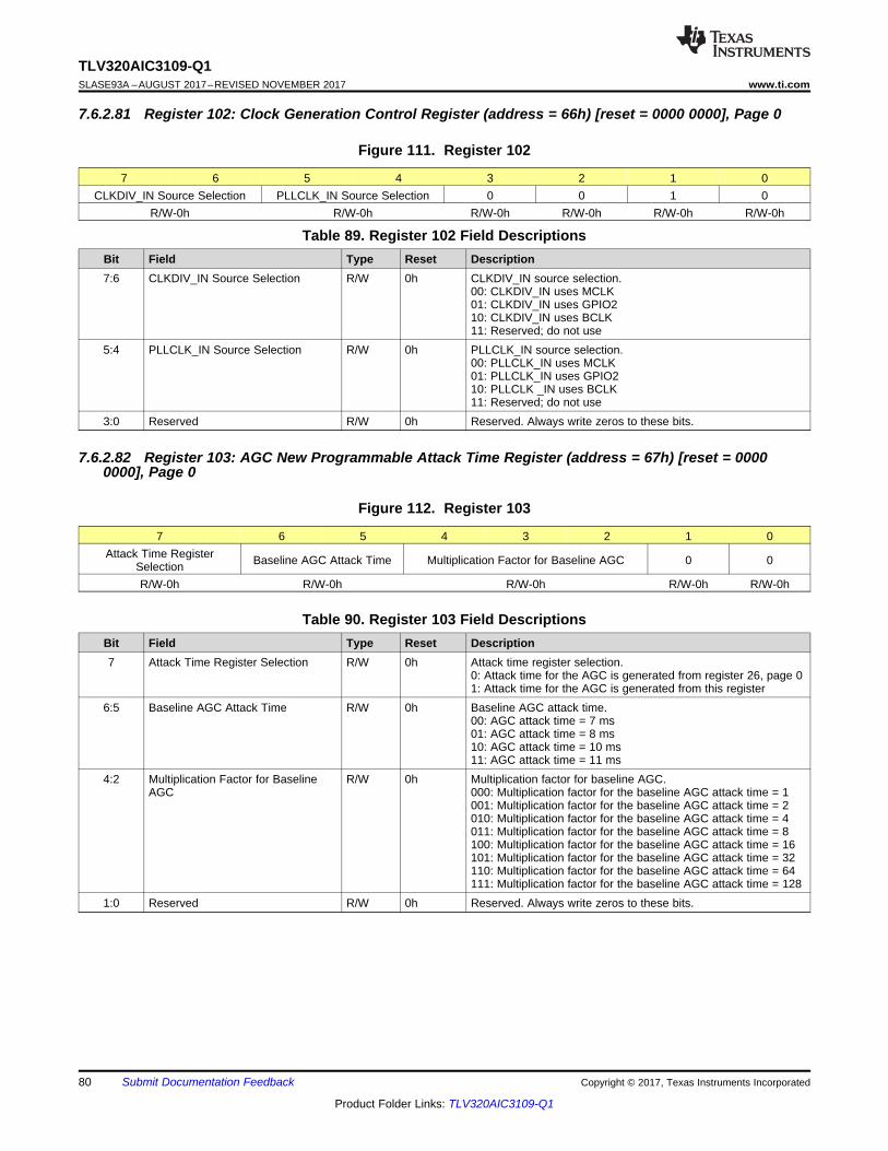
80
TLV320AIC3109-Q1SLASE93A –AUGUST 2017–REVISED NOVEMBER 2017 www.ti.com
Product Folder Links: TLV320AIC3109-Q1
Submit Documentation Feedback Copyright © 2017, Texas Instruments Incorporated
7.6.2.81 Register 102: Clock Generation Control Register (address = 66h) [reset = 0000 0000], Page 0
Figure 111. Register 102
7 6 5 4 3 2 1 0CLKDIV_IN Source Selection PLLCLK_IN Source Selection 0 0 1 0
R/W-0h R/W-0h R/W-0h R/W-0h R/W-0h R/W-0h
Table 89. Register 102 Field DescriptionsBit Field Type Reset Description7:6 CLKDIV_IN Source Selection R/W 0h CLKDIV_IN source selection.
00: CLKDIV_IN uses MCLK01: CLKDIV_IN uses GPIO210: CLKDIV_IN uses BCLK11: Reserved; do not use
5:4 PLLCLK_IN Source Selection R/W 0h PLLCLK_IN source selection.00: PLLCLK_IN uses MCLK01: PLLCLK_IN uses GPIO210: PLLCLK _IN uses BCLK11: Reserved; do not use
3:0 Reserved R/W 0h Reserved. Always write zeros to these bits.
7.6.2.82 Register 103: AGC New Programmable Attack Time Register (address = 67h) [reset = 00000000], Page 0
Figure 112. Register 103
7 6 5 4 3 2 1 0Attack Time Register
Selection Baseline AGC Attack Time Multiplication Factor for Baseline AGC 0 0
R/W-0h R/W-0h R/W-0h R/W-0h R/W-0h
Table 90. Register 103 Field DescriptionsBit Field Type Reset Description7 Attack Time Register Selection R/W 0h Attack time register selection.
0: Attack time for the AGC is generated from register 26, page 01: Attack time for the AGC is generated from this register
6:5 Baseline AGC Attack Time R/W 0h Baseline AGC attack time.00: AGC attack time = 7 ms01: AGC attack time = 8 ms10: AGC attack time = 10 ms11: AGC attack time = 11 ms
4:2 Multiplication Factor for BaselineAGC
R/W 0h Multiplication factor for baseline AGC.000: Multiplication factor for the baseline AGC attack time = 1001: Multiplication factor for the baseline AGC attack time = 2010: Multiplication factor for the baseline AGC attack time = 4011: Multiplication factor for the baseline AGC attack time = 8100: Multiplication factor for the baseline AGC attack time = 16101: Multiplication factor for the baseline AGC attack time = 32110: Multiplication factor for the baseline AGC attack time = 64111: Multiplication factor for the baseline AGC attack time = 128
1:0 Reserved R/W 0h Reserved. Always write zeros to these bits.

81
TLV320AIC3109-Q1www.ti.com SLASE93A –AUGUST 2017–REVISED NOVEMBER 2017
Product Folder Links: TLV320AIC3109-Q1
Submit Documentation FeedbackCopyright © 2017, Texas Instruments Incorporated
7.6.2.83 Register 104: AGC New Programmable Decay Time Register (address = 68h) [reset = 00000000], Page 0
Figure 113. Register 104
7 6 5 4 3 2 1 0Decay Time Register
Selection Baseline AGC Decay Time Multiplication Factor for Baseline AGC 0 0
R/W-0h R/W-0h R/W-0h R/W-0h R/W-0h
(1) Decay time is limited based on the NCODEC ratio that is selected. For NCODEC = 1, maximum decay time = 4 s; NCODEC = 1.5,maximum decay time = 5.6 s; NCODEC = 2, maximum decay time = 8 s; NCODEC = 2.5, maximum decay time = 9.6 s; NCODEC = 3or 3.5, maximum decay time = 11.2 s; NCODEC = 4 or 4.5, maximum decay time = 16 s; NCODEC = 5, maximum decay time = 19.2 s;and NCODEC = 5.5 or 6, maximum decay time = 22.4 s.
Table 91. Register 104 Field DescriptionsBit Field Type Reset Description7 Decay Time Register Selection (1) R/W 0h Decay time register selection.
0: Decay time for the AGC is generated from register 26, page 01: Decay time for the AGC is generated from this register
6:5 Baseline AGC Decay Time R/W 0h Baseline AGC decay time.00: AGC decay time = 50 ms01: AGC decay time = 150 ms10: AGC decay time = 250 ms11: -AGC decay time = 350 ms
4:2 Multiplication Factor for BaselineAGC
R/W 0h Multiplication factor for baseline AGC.000: Multiplication factor for the baseline AGC decay time = 1001: Multiplication factor for the baseline AGC decay time = 2010: Multiplication factor for the baseline AGC decay time = 4011: Multiplication factor for the baseline AGC decay time = 8100: Multiplication factor for the baseline AGC decay time = 16101: Multiplication factor for the baseline AGC decay time = 32110: Multiplication factor for the baseline AGC decay time = 64111: Multiplication factor for the baseline AGC decay time = 128
1:0 Reserved R/W 0h Reserved. Always write zeros to these bits.
7.6.2.84 Registers 105–106: Reserved (address = 69h–6Ah) [reset = 0000 0000], Page 0
Figure 114. Register 105
7 6 5 4 3 2 1 00 0 0 0 0 0 0 0
R/W-0h R/W-0h R/W-0h R/W-0h R/W-0h R/W-0h R/W-0h R/W-0h
Table 92. Register 105 Field DescriptionsBit Field Type Reset Description7:0 Reserved R/W 0h Reserved. Always write zeros to these bits.

82
TLV320AIC3109-Q1SLASE93A –AUGUST 2017–REVISED NOVEMBER 2017 www.ti.com
Product Folder Links: TLV320AIC3109-Q1
Submit Documentation Feedback Copyright © 2017, Texas Instruments Incorporated
7.6.2.85 Register 107: New Programmable ADC Digital Path and I2C Bus Condition Register (address =6Bh) [reset = 0000 0000], Page 0
Figure 115. Register 107
7 6 5 4 3 2 1 0Channel High-Pass
Filter CoefficientSelection
0 0 0ADC Digital Output toProgrammable Filter
Path Selection
I2C Bus ConditionDetector 0 I2C Bus Error
Detection Status
R/W-0h R/W-0h R/W-0h R/W-0h R/W-0h R/W-0h R-0h R-0h
Table 93. Register 107 Field DescriptionsBit Field Type Reset Description7 Channel High-Pass Filter Coefficient
SelectionR/W 0h Channel high-pass filter coefficient selection.
0: Default coefficients are used when ADC high pass is enabled1: Programmable coefficients are used when ADC high pass isenabled
6:4 Reserved R/W 0h Reserved. Always write zeros to these bits.3 ADC Digital Output to
Programmable Filter Path SelectionR/W 0h ADC digital output to programmable filter path selection.
0: No additional programmable filters other than the HPF areused for the ADC1: The programmable filter is connected to the ADC output ifboth DACs are powered down
2 I2C Bus Condition Detector R/W 0h I2C bus condition detector.0: Internal logic is enabled to detect an I2C bus error and clearsthe bus error condition1: Internal logic is disabled to detect an I2C bus error
1 Reserved R 0h Reserved. Always write zero to this bit0 I2C Bus Error Detection Status R 0h I2C bus error detection status.
0: I2C bus error is not detected1: I2C bus error is detected; this bit is cleared by reading thisregister
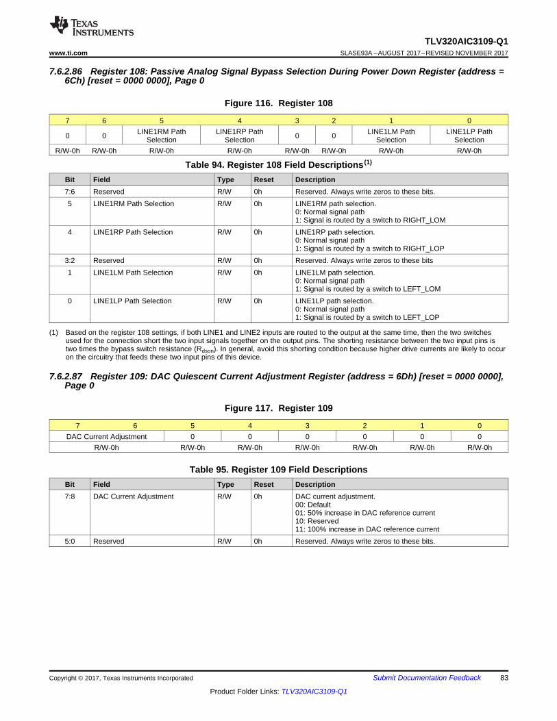
83
TLV320AIC3109-Q1www.ti.com SLASE93A –AUGUST 2017–REVISED NOVEMBER 2017
Product Folder Links: TLV320AIC3109-Q1
Submit Documentation FeedbackCopyright © 2017, Texas Instruments Incorporated
7.6.2.86 Register 108: Passive Analog Signal Bypass Selection During Power Down Register (address =6Ch) [reset = 0000 0000], Page 0
Figure 116. Register 108
7 6 5 4 3 2 1 0
0 0 LINE1RM PathSelection
LINE1RP PathSelection 0 0 LINE1LM Path
SelectionLINE1LP Path
SelectionR/W-0h R/W-0h R/W-0h R/W-0h R/W-0h R/W-0h R/W-0h R/W-0h
(1) Based on the register 108 settings, if both LINE1 and LINE2 inputs are routed to the output at the same time, then the two switchesused for the connection short the two input signals together on the output pins. The shorting resistance between the two input pins istwo times the bypass switch resistance (Rdson). In general, avoid this shorting condition because higher drive currents are likely to occuron the circuitry that feeds these two input pins of this device.
Table 94. Register 108 Field Descriptions (1)
Bit Field Type Reset Description7:6 Reserved R/W 0h Reserved. Always write zeros to these bits.5 LINE1RM Path Selection R/W 0h LINE1RM path selection.
0: Normal signal path1: Signal is routed by a switch to RIGHT_LOM
4 LINE1RP Path Selection R/W 0h LINE1RP path selection.0: Normal signal path1: Signal is routed by a switch to RIGHT_LOP
3:2 Reserved R/W 0h Reserved. Always write zeros to these bits1 LINE1LM Path Selection R/W 0h LINE1LM path selection.
0: Normal signal path1: Signal is routed by a switch to LEFT_LOM
0 LINE1LP Path Selection R/W 0h LINE1LP path selection.0: Normal signal path1: Signal is routed by a switch to LEFT_LOP
7.6.2.87 Register 109: DAC Quiescent Current Adjustment Register (address = 6Dh) [reset = 0000 0000],Page 0
Figure 117. Register 109
7 6 5 4 3 2 1 0DAC Current Adjustment 0 0 0 0 0 0
R/W-0h R/W-0h R/W-0h R/W-0h R/W-0h R/W-0h R/W-0h
Table 95. Register 109 Field DescriptionsBit Field Type Reset Description7:8 DAC Current Adjustment R/W 0h DAC current adjustment.
00: Default01: 50% increase in DAC reference current10: Reserved11: 100% increase in DAC reference current
5:0 Reserved R/W 0h Reserved. Always write zeros to these bits.

84
TLV320AIC3109-Q1SLASE93A –AUGUST 2017–REVISED NOVEMBER 2017 www.ti.com
Product Folder Links: TLV320AIC3109-Q1
Submit Documentation Feedback Copyright © 2017, Texas Instruments Incorporated
7.6.2.88 Registers 110–127: Reserved (address = 6Eh–7Fh) [reset = 0000 0000], Page 0
Figure 118. Registers 110–127
7 6 5 4 3 2 1 00 0 0 0 0 0 0 0
R-0h R-0h R-0h R-0h R-0h R-0h R-0h R-0h
Table 96. Registers 110–127 Field DescriptionsBit Field Type Reset Description7:0 Reserved R 0h Reserved. Always write zeros to these bits.
7.6.3 Page 1 Register DescriptionsThese registers are held within page 1.
7.6.3.1 Register 0: Page Select Register (address = 0h) [reset = 0000 0000], Page 1
Figure 119. Register 0
7 6 5 4 3 2 1 00 0 0 0 0 0 0 Page Select Bit
X-0h X-0h X-0h X-0h X-0h X-0h X-0h R/W-0h
Table 97. Register 0 Field DescriptionsBit Field Type Reset Description7:1 Reserved X 0h Reserved. Always write zeros to these bits.0 Page Select Bit R/W 0h Page select bit.
Writing zero to this bit sets page 0 as the active page forfollowing register accesses. Writing a one to this bit sets page 1as the active page for following register accesses. This registerbit is recommended to be read back after each write to ensurethat the proper page is being accessed for future registerread/writes. This register has the same functionality on page 0and page 1.
7.6.3.2 Register 1: Audio Effects Filter N0 Coefficient MSB Register (address = 1h) [reset = 0110 1011],Page 1
Figure 120. Register 1
7 6 5 4 3 2 1 0Audio Effects Filter N0 Coefficient MSB
R/W-0h R/W-1h R/W-1h R/W-0h R/W-1h R/W-0h R/W-1h R/W-1h
(1) When programming any coefficient value in page 1, always write the MSB register first, immediately followed by the LSB register. Evenif only the MSB or LSB of the coefficient changes, write both registers in this sequence.
Table 98. Register 1 Field DescriptionsBit Field Type Reset Description7:0 Audio Effects Filter N0 Coefficient
MSB (1)R/W 0110 1011h Audio effects filter N0 coefficient MSB.
The 16-bit integer contained in the MSB and LSB registersfor this coefficient are interpreted as a 2's-complementinteger with possible values ranging from –32,768 to 32,767.
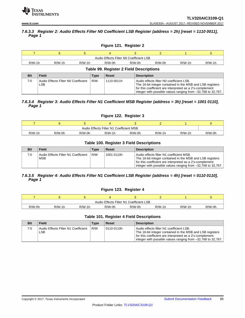
85
TLV320AIC3109-Q1www.ti.com SLASE93A –AUGUST 2017–REVISED NOVEMBER 2017
Product Folder Links: TLV320AIC3109-Q1
Submit Documentation FeedbackCopyright © 2017, Texas Instruments Incorporated
7.6.3.3 Register 2: Audio Effects Filter N0 Coefficient LSB Register (address = 2h) [reset = 1110 0011],Page 1
Figure 121. Register 2
7 6 5 4 3 2 1 0Audio Effects Filter N0 Coefficient LSB
R/W-1h R/W-1h R/W-1h R/W-0h R/W-0h R/W-0h R/W-1h R/W-1h
Table 99. Register 2 Field DescriptionsBit Field Type Reset Description7:0 Audio Effects Filter N0 Coefficient
LSBR/W 1110 0011h Audio effects filter N0 coefficient LSB.
The 16-bit integer contained in the MSB and LSB registersfor this coefficient are interpreted as a 2's-complementinteger with possible values ranging from –32,768 to 32,767.
7.6.3.4 Register 3: Audio Effects Filter N1 Coefficient MSB Register (address = 3h) [reset = 1001 0110],Page 1
Figure 122. Register 3
7 6 5 4 3 2 1 0Audio Effects Filter N1 Coefficient MSB
R/W-1h R/W-0h R/W-0h R/W-1h R/W-0h R/W-1h R/W-1h R/W-0h
Table 100. Register 3 Field DescriptionsBit Field Type Reset Description7:0 Audio Effects Filter N1 Coefficient
MSBR/W 1001 0110h Audio effects filter N1 coefficient MSB.
The 16-bit integer contained in the MSB and LSB registersfor this coefficient are interpreted as a 2's-complementinteger with possible values ranging from –32,768 to 32,767.
7.6.3.5 Register 4: Audio Effects Filter N1 Coefficient LSB Register (address = 4h) [reset = 0110 0110],Page 1
Figure 123. Register 4
7 6 5 4 3 2 1 0Audio Effects Filter N1 Coefficient LSB
R/W-0h R/W-1h R/W-1h R/W-0h R/W-0h R/W-1h R/W-1h R/W-0h
Table 101. Register 4 Field DescriptionsBit Field Type Reset Description7:0 Audio Effects Filter N1 Coefficient
LSBR/W 0110 0110h Audio effects filter N1 coefficient LSB.
The 16-bit integer contained in the MSB and LSB registersfor this coefficient are interpreted as a 2's-complementinteger with possible values ranging from –32,768 to 32,767.

86
TLV320AIC3109-Q1SLASE93A –AUGUST 2017–REVISED NOVEMBER 2017 www.ti.com
Product Folder Links: TLV320AIC3109-Q1
Submit Documentation Feedback Copyright © 2017, Texas Instruments Incorporated
7.6.3.6 Register 5: Audio Effects Filter N2 Coefficient MSB Register (address = 5h) [reset = 0110 0111],Page 1
Figure 124. Register 5
7 6 5 4 3 2 1 0Audio Effects Filter N2 Coefficient MSB
R/W-0h R/W-1h R/W-1h R/W-0h R/W-0h R/W-1h R/W-1h R/W-1h
Table 102. Register 5 Field DescriptionsBit Field Type Reset Description7:0 Audio Effects Filter N2 Coefficient
MSBR/W 0110 0111h Audio effects filter N2 coefficient MSB.
The 16-bit integer contained in the MSB and LSB registersfor this coefficient are interpreted as a 2's-complementinteger with possible values ranging from –32,768 to 32,767.
7.6.3.7 Register 6: Audio Effects Filter N2 Coefficient LSB Register (address = 6h) [reset = 0101 1101],Page 1
Figure 125. Register 6
7 6 5 4 3 2 1 0Audio Effects Filter N2 Coefficient LSB
R/W-0h R/W-1h R/W-0h R/W-1h R/W-1h R/W-1h R/W-0h R/W-1h
Table 103. Register 6 Field DescriptionsBit Field Type Reset Description7:0 Audio Effects Filter N2 Coefficient
LSBR/W 0101 1101h Audio effects filter N2 coefficient LSB.
The 16-bit integer contained in the MSB and LSB registersfor this coefficient are interpreted as a 2's-complementinteger with possible values ranging from –32,768 to 32,767.
7.6.3.8 Register 7: Audio Effects Filter N3 Coefficient MSB Register (address = 7h) [reset = 0110 1011],Page 1
Figure 126. Register 7
7 6 5 4 3 2 1 0Audio Effects Filter N3 Coefficient MSB
R/W-0h R/W-1h R/W-1h R/W-0h R/W-1h R/W-0h R/W-1h R/W-1h
Table 104. Register 7 Field DescriptionsBit Field Type Reset Description7:0 Audio Effects Filter N3 Coefficient
MSBR/W 0110 1011h Audio effects filter N3 coefficient MSB.
The 16-bit integer contained in the MSB and LSB registersfor this coefficient are interpreted as a 2's-complementinteger with possible values ranging from –32,768 to 32,767.

87
TLV320AIC3109-Q1www.ti.com SLASE93A –AUGUST 2017–REVISED NOVEMBER 2017
Product Folder Links: TLV320AIC3109-Q1
Submit Documentation FeedbackCopyright © 2017, Texas Instruments Incorporated
7.6.3.9 Register 8: Audio Effects Filter N3 Coefficient LSB Register (address = 8h) [reset = 1110 0011],Page 1
Figure 127. Register 8
7 6 5 4 3 2 1 0Audio Effects Filter N3 Coefficient LSB
R/W-1h R/W-1h R/W-1h R/W-0h R/W-0h R/W-0h R/W-1h R/W-1h
Table 105. Register 8 Field DescriptionsBit Field Type Reset Description7:0 Audio Effects Filter N3 Coefficient
LSBR/W 1110 0011h Audio effects filter N3 coefficient LSB.
The 16-bit integer contained in the MSB and LSB registersfor this coefficient are interpreted as a 2's-complementinteger with possible values ranging from –32,768 to 32,767.
7.6.3.10 Register 9: Audio Effects Filter N4 Coefficient MSB Register (address = 9h) [reset = 1001 0110],Page 1
Figure 128. Register 9
7 6 5 4 3 2 1 0Audio Effects Filter N4 Coefficient MSB
R/W-1h R/W-0h R/W-0h R/W-1h R/W-0h R/W-1h R/W-1h R/W-0h
Table 106. Register 9 Field DescriptionsBit Field Type Reset Description7:0 Audio Effects Filter N4 Coefficient
MSBR/W 1001 0110h Audio effects filter N4 coefficient MSB.
The 16-bit integer contained in the MSB and LSB registersfor this coefficient are interpreted as a 2's-complementinteger with possible values ranging from –32,768 to 32,767.
7.6.3.11 Register 10: Audio Effects Filter N4 Coefficient LSB Register (address = Ah) [reset = 0110 0110],Page 1
Figure 129. Register 10
7 6 5 4 3 2 1 0Audio Effects Filter N4 Coefficient LSB
R/W-0h R/W-1h R/W-1h R/W-0h R/W-0h R/W-1h R/W-1h R/W-0h
Table 107. Register 10 Field DescriptionsBit Field Type Reset Description7:0 Audio Effects Filter N4 Coefficient
LSBR/W 0110 0110h Audio effects filter N4 coefficient LSB.
The 16-bit integer contained in the MSB and LSB registersfor this coefficient are interpreted as a 2's-complementinteger with possible values ranging from –32,768 to 32,767.
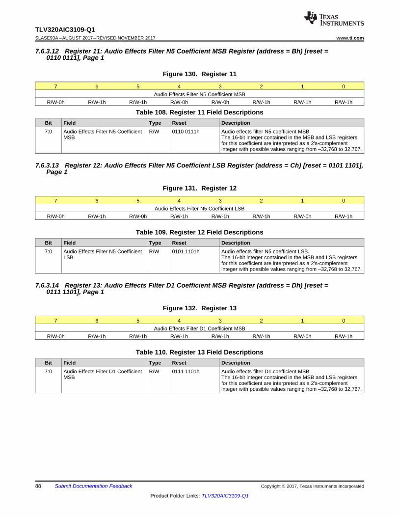
88
TLV320AIC3109-Q1SLASE93A –AUGUST 2017–REVISED NOVEMBER 2017 www.ti.com
Product Folder Links: TLV320AIC3109-Q1
Submit Documentation Feedback Copyright © 2017, Texas Instruments Incorporated
7.6.3.12 Register 11: Audio Effects Filter N5 Coefficient MSB Register (address = Bh) [reset =0110 0111], Page 1
Figure 130. Register 11
7 6 5 4 3 2 1 0Audio Effects Filter N5 Coefficient MSB
R/W-0h R/W-1h R/W-1h R/W-0h R/W-0h R/W-1h R/W-1h R/W-1h
Table 108. Register 11 Field DescriptionsBit Field Type Reset Description7:0 Audio Effects Filter N5 Coefficient
MSBR/W 0110 0111h Audio effects filter N5 coefficient MSB.
The 16-bit integer contained in the MSB and LSB registersfor this coefficient are interpreted as a 2's-complementinteger with possible values ranging from –32,768 to 32,767.
7.6.3.13 Register 12: Audio Effects Filter N5 Coefficient LSB Register (address = Ch) [reset = 0101 1101],Page 1
Figure 131. Register 12
7 6 5 4 3 2 1 0Audio Effects Filter N5 Coefficient LSB
R/W-0h R/W-1h R/W-0h R/W-1h R/W-1h R/W-1h R/W-0h R/W-1h
Table 109. Register 12 Field DescriptionsBit Field Type Reset Description7:0 Audio Effects Filter N5 Coefficient
LSBR/W 0101 1101h Audio effects filter N5 coefficient LSB.
The 16-bit integer contained in the MSB and LSB registersfor this coefficient are interpreted as a 2's-complementinteger with possible values ranging from –32,768 to 32,767.
7.6.3.14 Register 13: Audio Effects Filter D1 Coefficient MSB Register (address = Dh) [reset =0111 1101], Page 1
Figure 132. Register 13
7 6 5 4 3 2 1 0Audio Effects Filter D1 Coefficient MSB
R/W-0h R/W-1h R/W-1h R/W-1h R/W-1h R/W-1h R/W-0h R/W-1h
Table 110. Register 13 Field DescriptionsBit Field Type Reset Description7:0 Audio Effects Filter D1 Coefficient
MSBR/W 0111 1101h Audio effects filter D1 coefficient MSB.
The 16-bit integer contained in the MSB and LSB registersfor this coefficient are interpreted as a 2's-complementinteger with possible values ranging from –32,768 to 32,767.

89
TLV320AIC3109-Q1www.ti.com SLASE93A –AUGUST 2017–REVISED NOVEMBER 2017
Product Folder Links: TLV320AIC3109-Q1
Submit Documentation FeedbackCopyright © 2017, Texas Instruments Incorporated
7.6.3.15 Register 14: Audio Effects Filter D1 Coefficient LSB Register (address = Eh) [reset =1000 0011h], Page 1
Figure 133. Register 14
7 6 5 4 3 2 1 0Audio Effects Filter D1 Coefficient LSB
R/W-1h R/W-0h R/W-0h R/W-0h R/W-0h R/W-0h R/W-1h R/W-1h
Table 111. Register 14 Field DescriptionsBit Field Type Reset Description7:0 Audio Effects Filter D1 Coefficient
LSBR/W 1000 0011h Audio effects filter D1 coefficient LSB.
The 16-bit integer contained in the MSB and LSB registersfor this coefficient are interpreted as a 2's-complementinteger with possible values ranging from –32,768 to 32,767.
7.6.3.16 Register 15: Audio Effects Filter D2 Coefficient MSB Register (address = Fh) [reset = 1000 0100],Page 1
Figure 134. Register 15
7 6 5 4 3 2 1 0Audio Effects Filter D2 Coefficient MSB
R/W-1h R/W-0h R/W-0h R/W-0h R/W-0h R/W-1h R/W-0h R/W-0h
Table 112. Register 15 Field DescriptionsBit Field Type Reset Description7:0 Audio Effects Filter D2 Coefficient
MSBR/W 1000 0100h Audio effects filter D2 coefficient MSB.
The 16-bit integer contained in the MSB and LSB registersfor this coefficient are interpreted as a 2's-complementinteger with possible values ranging from –32,768 to 32,767.
7.6.3.17 Register 16: Audio Effects Filter D2 Coefficient LSB Register (address = 10h) [reset =1110 1110], Page 1
Figure 135. Register 16
7 6 5 4 3 2 1 0Audio Effects Filter D2 Coefficient LSB
R/W-1h R/W-1h R/W-1h R/W-0h R/W-1h R/W-1h R/W-1h R/W-0h
Table 113. Register 16 Field DescriptionsBit Field Type Reset Description7:0 Audio Effects Filter D2 Coefficient
LSBR/W 1110 1110h Audio effects filter D2 coefficient LSB.
The 16-bit integer contained in the MSB and LSB registersfor this coefficient are interpreted as a 2's-complementinteger with possible values ranging from –32,768 to 32,767.

90
TLV320AIC3109-Q1SLASE93A –AUGUST 2017–REVISED NOVEMBER 2017 www.ti.com
Product Folder Links: TLV320AIC3109-Q1
Submit Documentation Feedback Copyright © 2017, Texas Instruments Incorporated
7.6.3.18 Register 17: Audio Effects Filter D4 Coefficient MSB Register (address = 11h) [reset =0111 1101], Page 1
Figure 136. Register 17
7 6 5 4 3 2 1 0Audio Effects Filter D4 Coefficient MSB
R/W-0h R/W-1h R/W-1h R/W-1h R/W-1h R/W-1h R/W-0h R/W-1h
Table 114. Register 17 Field DescriptionsBit Field Type Reset Description7:0 Audio Effects Filter D4 Coefficient
MSBR/W 0111 1101h Audio effects filter D4 coefficient MSB.
The 16-bit integer contained in the MSB and LSB registersfor this coefficient are interpreted as a 2's-complementinteger with possible values ranging from –32,768 to 32,767.
7.6.3.19 Register 18: Audio Effects Filter D4 Coefficient LSB Register (address = 12h) [reset =1000 0011], Page 1
Figure 137. Register 18
7 6 5 4 3 2 1 0Audio Effects Filter D4 Coefficient LSB
R/W-1h R/W-0h R/W-0h R/W-0h R/W-0h R/W-0h R/W-1h R/W-1h
Table 115. Register 18 Field DescriptionsBit Field Type Reset Description7:0 Audio Effects Filter D4 Coefficient
LSBR/W 1000 0011h Audio effects filter D4 coefficient LSB.
The 16-bit integer contained in the MSB and LSB registersfor this coefficient are interpreted as a 2's-complementinteger with possible values ranging from –32,768 to 32,767.
7.6.3.20 Register 19: Audio Effects Filter D5 Coefficient MSB Register (address = 13h) [reset =1000 0100], Page 1
Figure 138. Register 19
7 6 5 4 3 2 1 0Audio Effects Filter D5 Coefficient MSB
R/W-1h R/W-0h R/W-0h R/W-0h R/W-0h R/W-1h R/W-0h R/W-0h
Table 116. Register 19 Field DescriptionsBit Field Type Reset Description7:0 Audio Effects Filter D5 Coefficient
MSBR/W 1000 0100h Audio effects filter D5 coefficient MSB.
The 16-bit integer contained in the MSB and LSB registersfor this coefficient are interpreted as a 2's-complementinteger with possible values ranging from –32,768 to 32,767.

91
TLV320AIC3109-Q1www.ti.com SLASE93A –AUGUST 2017–REVISED NOVEMBER 2017
Product Folder Links: TLV320AIC3109-Q1
Submit Documentation FeedbackCopyright © 2017, Texas Instruments Incorporated
7.6.3.21 Register 20: Audio Effects Filter D5 Coefficient LSB Register (address = 14h) [reset =1110 1110], Page 1
Figure 139. Register 20
7 6 5 4 3 2 1 0Audio Effects Filter D5 Coefficient LSB
R/W-1h R/W-1h R/W-1h R/W-0h R/W-1h R/W-1h R/W-1h R/W-0h
Table 117. Register 20 Field DescriptionsBit Field Type Reset Description7:0 Audio Effects Filter D5 Coefficient
LSBR/W 1110 1110h Audio effects filter D5 coefficient LSB.
The 16-bit integer contained in the MSB and LSB registersfor this coefficient are interpreted as a 2's-complementinteger with possible values ranging from –32,768 to 32,767.
7.6.3.22 Register 21: De-Emphasis Filter N0 Coefficient MSB Register (address = 15h) [reset =0011 1001], Page 1
Figure 140. Register 21
7 6 5 4 3 2 1 0De-Emphasis Filter N0 Coefficient MSB
R/W-0h R/W-0h R/W-1h R/W-1h R/W-1h R/W-0h R/W-0h R/W-1h
Table 118. Register 21 Field DescriptionsBit Field Type Reset Description7:0 De-Emphasis Filter N0 Coefficient
MSBR/W 0011 1001h De-emphasis filter N0 coefficient MSB.
The 16-bit integer contained in the MSB and LSB registersfor this coefficient are interpreted as a 2's-complementinteger with possible values ranging from –32,768 to 32,767.
7.6.3.23 Register 22: De-Emphasis Filter N0 Coefficient LSB Register (address = 16h) [reset =0101 0101], Page 1
Figure 141. Register 22
7 6 5 4 3 2 1 0De-Emphasis Filter N0 Coefficient LSB
R/W-0h R/W-1h R/W-0h R/W-1h R/W-0h R/W-1h R/W-0h R/W-1h
Table 119. Register 22 Field DescriptionsBit Field Type Reset Description7:0 De-Emphasis Filter N0 Coefficient
LSBR/W 0101 0101h De-emphasis filter N0 coefficient LSB.
The 16-bit integer contained in the MSB and LSB registersfor this coefficient are interpreted as a 2's-complementinteger with possible values ranging from –32,768 to 32,767.

92
TLV320AIC3109-Q1SLASE93A –AUGUST 2017–REVISED NOVEMBER 2017 www.ti.com
Product Folder Links: TLV320AIC3109-Q1
Submit Documentation Feedback Copyright © 2017, Texas Instruments Incorporated
7.6.3.24 Register 23: De-Emphasis Filter N1 Coefficient MSB Register (address = 17h) [reset =1111 0011], Page 1
Figure 142. Register 23
7 6 5 4 3 2 1 0De-Emphasis Filter N1 Coefficient MSB
R/W-1h R/W-1h R/W-1h R/W-1h R/W-0h R/W-0h R/W-1h R/W-1h
Table 120. Register 23 Field DescriptionsBit Field Type Reset Description7:0 De-Emphasis Filter N1 Coefficient
MSBR/W 1111 0011h De-emphasis filter N1 coefficient MSB.
The 16-bit integer contained in the MSB and LSB registersfor this coefficient are interpreted as a 2's-complementinteger with possible values ranging from –32,768 to 32,767.
7.6.3.25 Register 24: De-Emphasis Filter N1 Coefficient LSB Register (address = 18h) [reset =0010 1101], Page 1
Figure 143. Register 24
7 6 5 4 3 2 1 0De-Emphasis Filter N1 Coefficient LSB
R/W-0h R/W-0h R/W-1h R/W-0h R/W-1h R/W-1h R/W-0h R/W-1h
Table 121. Register 24 Field DescriptionsBit Field Type Reset Description7:0 De-Emphasis Filter N1 Coefficient
LSBR/W 0010 1101h De-emphasis filter N1 coefficient LSB.
The 16-bit integer contained in the MSB and LSB registersfor this coefficient are interpreted as a 2's-complementinteger with possible values ranging from –32,768 to 32,767.
7.6.3.26 Register 25: De-Emphasis Filter D1 Coefficient MSB Register (address = 19h) [reset =0101 0011], Page 1
Figure 144. Register 25
7 6 5 4 3 2 1 0De-Emphasis Filter D1 Coefficient MSB
R/W-0h R/W-1h R/W-0h R/W-1h R/W-0h R/W-0h R/W-1h R/W-1h
Table 122. Register 25 Field DescriptionsBit Field Type Reset Description7:0 De-Emphasis Filter D1 Coefficient
MSBR/W 0101 0011h De-emphasis filter D1 coefficient MSB.
The 16-bit integer contained in the MSB and LSB registersfor this coefficient are interpreted as a 2's-complementinteger with possible values ranging from –32,768 to 32,767.
93
TLV320AIC3109-Q1www.ti.com SLASE93A –AUGUST 2017–REVISED NOVEMBER 2017
Product Folder Links: TLV320AIC3109-Q1
Submit Documentation FeedbackCopyright © 2017, Texas Instruments Incorporated
7.6.3.27 Register 26: De-Emphasis Filter D1 Coefficient LSB Register (address = 1Ah) [reset =0111 1110], Page 1
Figure 145. Register 26
7 6 5 4 3 2 1 0De-Emphasis Filter D1 Coefficient LSB
R/W-0h R/W-1h R/W-1h R/W-1h R/W-1h R/W-1h R/W-1h R/W-0h
Table 123. Register 26 Field DescriptionsBit Field Type Reset Description7:0 De-Emphasis Filter D1 Coefficient
LSBR/W 0111 1110h De-emphasis filter D1 coefficient LSB.
The 16-bit integer contained in the MSB and LSB registersfor this coefficient are interpreted as a 2's-complementinteger with possible values ranging from –32,768 to 32,767.
7.6.3.28 Register 27: Reserved (address = 1Bh) [reset = 0110 1011], Page 1
Figure 146. Register 27
7 6 5 4 3 2 1 00 1 1 0 1 0 1 1
R/W-0h R/W-1h R/W-1h R/W-0h R/W-1h R/W-0h R/W-1h R/W-1h
Table 124. Register 27 Field DescriptionsBit Field Type Reset Description7:0 Reserved R/W 0110 1011h Reserved. Always write 0110 1011 to these bits.
7.6.3.29 Register 28: Reserved (address = 1Ch) [reset = 1110 0011], Page 1
Figure 147. Register 28
7 6 5 4 3 2 1 01 1 1 0 0 0 1 1
R/W-1h R/W-1h R/W-1h R/W-0h R/W-0h R/W-0h R/W-1h R/W-1h
Table 125. Register 28 Field DescriptionsBit Field Type Reset Description7:0 Reserved R/W 1110 0011h Reserved. Always write 1110 0011 to these bits.
7.6.3.30 Register 29: Reserved (address = 1Dh) [reset = 1001 0110], Page 1
Figure 148. Register 29
7 6 5 4 3 2 1 01 0 0 1 0 1 1 0
R/W-1h R/W-0h R/W-0h R/W-1h R/W-0h R/W-1h R/W-1h R/W-0h
Table 126. Register 29 Field DescriptionsBit Field Type Reset Description7:0 Reserved R/W 1001 0110h Reserved. Always write 1001 0110 to these bits.

94
TLV320AIC3109-Q1SLASE93A –AUGUST 2017–REVISED NOVEMBER 2017 www.ti.com
Product Folder Links: TLV320AIC3109-Q1
Submit Documentation Feedback Copyright © 2017, Texas Instruments Incorporated
7.6.3.31 Register 30: Reserved (address = 1Eh) [reset = 0110 0110], Page 1
Figure 149. Register 30
7 6 5 4 3 2 1 00 1 1 0 0 1 1 0
R/W-0h R/W-1h R/W-1h R/W-0h R/W-0h R/W-1h R/W-1h R/W-0h
Table 127. Register 30 Field DescriptionsBit Field Type Reset Description7:0 Reserved R/W 0110 0110h Reserved. Always write 0110 0110 to these bits.
7.6.3.32 Register 31: Reserved (address = 1Fh) [reset = 0110 0111], Page 1
Figure 150. Register 31
7 6 5 4 3 2 1 00 1 1 0 0 1 1 1
R/W-0h R/W-1h R/W-1h R/W-0h R/W-0h R/W-1h R/W-1h R/W-1h
Table 128. Register 31 Field DescriptionsBit Field Type Reset Description7:0 Reserved R/W 0110 0111h Reserved. Always write 0110 0111 to these bits.
7.6.3.33 Register 32: Reserved (address = 20h) [reset = 0101 1101], Page 1
Figure 151. Register 32
7 6 5 4 3 2 1 00 1 0 1 1 1 0 1
R/W-0h R/W-1h R/W-0h R/W-1h R/W-1h R/W-1h R/W-0h R/W-1h
Table 129. Register 32 Field DescriptionsBit Field Type Reset Description7:0 Reserved R/W 0101 1101h Reserved. Always write 0101 1101 to these bits.
7.6.3.34 Register 33: Reserved (address = 21h) [reset = 0110 1011], Page 1
Figure 152. Register 33
7 6 5 4 3 2 1 00 1 1 0 1 0 1 1
R/W-0h R/W-1h R/W-1h R/W-0h R/W-1h R/W-0h R/W-1h R/W-1h
Table 130. Register 33 Field DescriptionsBit Field Type Reset Description7:0 Reserved R/W 0110 1011h Reserved. Always write 0110 1011 to these bits.
95
TLV320AIC3109-Q1www.ti.com SLASE93A –AUGUST 2017–REVISED NOVEMBER 2017
Product Folder Links: TLV320AIC3109-Q1
Submit Documentation FeedbackCopyright © 2017, Texas Instruments Incorporated
7.6.3.35 Register 34: Reserved (address = 22h) [reset = 1110 0011], Page 1
Figure 153. Register 34
7 6 5 4 3 2 1 01 1 1 0 0 0 1 1
R/W-1h R/W-1h R/W-1h R/W-0h R/W-0h R/W-0h R/W-1h R/W-1h
Table 131. Register 34 Field DescriptionsBit Field Type Reset Description7:0 Reserved R/W 1110 0011h Reserved. Always write 1110 0011 to these bits.
7.6.3.36 Register 35: Reserved (address = 23h) [reset = 1001 0110], Page 1
Figure 154. Register 35
7 6 5 4 3 2 1 01 0 0 1 0 1 1 0
R/W-1h R/W-0h R/W-0h R/W-1h R/W-0h R/W-1h R/W-1h R/W-0h
Table 132. Register 35 Field DescriptionsBit Field Type Reset Description7:0 Reserved R/W 1001 0110h Reserved. Always write 1001 0110 to these bits.
7.6.3.37 Register 36: Reserved (address = 24h) [reset = 0110 0110], Page 1
Figure 155. Register 36
7 6 5 4 3 2 1 00 1 1 0 0 1 1 0
R/W-0h R/W-1h R/W-1h R/W-0h R/W-0h R/W-1h R/W-1h R/W-0h
Table 133. Register 36 Field DescriptionsBit Field Type Reset Description7:0 Reserved R/W 0110 0110h Reserved. Always write 0110 0110 to these bits.
7.6.3.38 Register 37: Reserved (address = 25h) [reset = 0110 0111], Page 1
Figure 156. Register 37
7 6 5 4 3 2 1 00 1 1 0 0 1 1 1
R/W-0h R/W-1h R/W-1h R/W-0h R/W-0h R/W-1h R/W-1h R/W-1h
Table 134. Register 37 Field DescriptionsBit Field Type Reset Description7:0 Reserved R/W 0110 0111h Reserved. Always write 0110 0111 to these bits.

96
TLV320AIC3109-Q1SLASE93A –AUGUST 2017–REVISED NOVEMBER 2017 www.ti.com
Product Folder Links: TLV320AIC3109-Q1
Submit Documentation Feedback Copyright © 2017, Texas Instruments Incorporated
7.6.3.39 Register 38: Reserved (address = 26h) [reset = 0101 1101], Page 1
Figure 157. Register 38
7 6 5 4 3 2 1 00 1 0 1 1 1 0 1
R/W-0h R/W-1h R/W-0h R/W-1h R/W-1h R/W-1h R/W-0h R/W-1h
Table 135. Register 38 Field DescriptionsBit Field Type Reset Description7:0 Reserved R/W 0101 1101h Reserved. Always write 0101 1101 to these bits.
7.6.3.40 Register 39: Reserved (address = 27h) [reset = 0111 1101], Page 1
Figure 158. Register 39
7 6 5 4 3 2 1 00 1 1 1 1 1 0 1
R/W-0h R/W-1h R/W-1h R/W-1h R/W-1h R/W-1h R/W-0h R/W-1h
Table 136. Register 39 Field DescriptionsBit Field Type Reset Description7:0 Reserved R/W 0111 1101h Reserved. Always write 0111 1101 to these bits.
7.6.3.41 Register 40: Reserved (address = 28h) [reset = 1000 0011], Page 1
Figure 159. Register 40
7 6 5 4 3 2 1 01 0 0 0 0 0 1 1
R/W-1h R/W-0h R/W-0h R/W-0h R/W-0h R/W-0h R/W-1h R/W-1h
Table 137. Register 40 Field DescriptionsBit Field Type Reset Description7:0 Reserved R/W 1000 0011h Reserved. Always write 1000 0011 to these bits.
7.6.3.42 Register 41: Reserved (address = 29h) [reset = 1000 0100], Page 1
Figure 160. Register 41
7 6 5 4 3 2 1 01 0 0 0 0 1 0 0
R/W-1h R/W-0h R/W-0h R/W-0h R/W-0h R/W-1h R/W-0h R/W-0h
Table 138. Register 41 Field DescriptionsBit Field Type Reset Description7:0 Reserved R/W 1000 0100h Reserved. Always write 1000 0100 to these bits.
97
TLV320AIC3109-Q1www.ti.com SLASE93A –AUGUST 2017–REVISED NOVEMBER 2017
Product Folder Links: TLV320AIC3109-Q1
Submit Documentation FeedbackCopyright © 2017, Texas Instruments Incorporated
7.6.3.43 Register 42: Reserved (address = 2Ah) [reset = 1110 1110], Page 1
Figure 161. Register 42
7 6 5 4 3 2 1 01 1 1 0 1 1 1 0
R/W-1h R/W-1h R/W-1h R/W-0h R/W-1h R/W-1h R/W-1h R/W-0h
Table 139. Register 42 Field DescriptionsBit Field Type Reset Description7:0 Reserved R/W 1110 1110h Reserved. Always write 1110 1110 to these bits.
7.6.3.44 Register 43: Reserved (address = 2Bh) [reset = 0111 1101], Page 1
Figure 162. Register 43
7 6 5 4 3 2 1 00 1 1 1 1 1 0 1
R/W-0h R/W-1h R/W-1h R/W-1h R/W-1h R/W-1h R/W-0h R/W-1h
Table 140. Register 43 Field DescriptionsBit Field Type Reset Description7:0 Reserved R/W 0111 1101h Reserved. Always write 0111 1101 to these bits.
7.6.3.45 Register 44: Reserved (address = 2Ch) [reset = 1000 0011], Page 1
Figure 163. Register 44
7 6 5 4 3 2 1 01 0 0 0 0 0 1 1
R/W-1h R/W-0h R/W-0h R/W-0h R/W-0h R/W-0h R/W-1h R/W-1h
Table 141. Register 44 Field DescriptionsBit Field Type Reset Description7:0 Reserved R/W 1000 0011h Reserved. Always write 1000 0011 to these bits.
7.6.3.46 Register 45: Reserved (address = 2Dh) [reset = 1000 0100], Page 1
Figure 164. Register 45
7 6 5 4 3 2 1 01 0 0 0 0 1 0 0
R/W-1h R/W-0h R/W-0h R/W-0h R/W-0h R/W-1h R/W-0h R/W-0h
Table 142. Register 45 Field DescriptionsBit Field Type Reset Description7:0 Reserved R/W 1000 0100h Reserved. Always write 1000 0100 to these bits.

98
TLV320AIC3109-Q1SLASE93A –AUGUST 2017–REVISED NOVEMBER 2017 www.ti.com
Product Folder Links: TLV320AIC3109-Q1
Submit Documentation Feedback Copyright © 2017, Texas Instruments Incorporated
7.6.3.47 Register 46: Reserved (address = 2Eh) [reset = 1110 1110], Page 1
Figure 165. Register 46
7 6 5 4 3 2 1 01 1 1 0 1 1 1 0
R/W-1h R/W-1h R/W-1h R/W-0h R/W-1h R/W-1h R/W-1h R/W-0h
Table 143. Register 46 Field DescriptionsBit Field Type Reset Description7:0 Reserved R/W 1110 1110h Reserved. Always write 1110 1110 to these bits.
7.6.3.48 Register 47: Reserved (address = 2Fh) [reset = 0011 1001], Page 1
Figure 166. Register 47
7 6 5 4 3 2 1 00 0 1 1 1 0 0 1
R/W-0h R/W-0h R/W-1h R/W-1h R/W-1h R/W-0h R/W-0h R/W-1h
Table 144. Register 47 Field DescriptionsBit Field Type Reset Description7:0 Reserved R/W 0011 1001h Reserved. Always write 0011 1001 to these bits.
7.6.3.49 Register 48: Reserved (address = 30h) [reset = 0101 0101], Page 1
Figure 167. Register 48
7 6 5 4 3 2 1 00 1 0 1 0 1 0 1
R/W-0h R/W-1h R/W-0h R/W-1h R/W-0h R/W-1h R/W-0h R/W-1h
Table 145. Register 48 Field DescriptionsBit Field Type Reset Description7:0 Reserved R/W 0101 0101h Reserved. Always write 0101 0101 to these bits.
7.6.3.50 Register 49: Reserved (address = 31h) [reset = 1111 0011], Page 1
Figure 168. Register 49
7 6 5 4 3 2 1 01 1 1 1 0 0 1 1
R/W-1h R/W-1h R/W-1h R/W-1h R/W-0h R/W-0h R/W-1h R/W-1h
Table 146. Register 49 Field DescriptionsBit Field Type Reset Description7:0 Reserved R/W 1111 0011h Reserved. Always write 1111 0011 to these bits.
99
TLV320AIC3109-Q1www.ti.com SLASE93A –AUGUST 2017–REVISED NOVEMBER 2017
Product Folder Links: TLV320AIC3109-Q1
Submit Documentation FeedbackCopyright © 2017, Texas Instruments Incorporated
7.6.3.51 Register 50: Reserved (address = 32h) [reset = 0010 1101], Page 1
Figure 169. Register 50
7 6 5 4 3 2 1 00 0 1 0 1 1 0 1
R/W-0h R/W-0h R/W-1h R/W-0h R/W-1h R/W-1h R/W-0h R/W-1h
Table 147. Register 50 Field DescriptionsBit Field Type Reset Description7:0 Reserved R/W 0010 1101h Reserved. Always write 0010 1101 to these bits.
7.6.3.52 Register 51: Reserved (address = 33h) [reset = 0101 0011], Page 1
Figure 170. Register 51
7 6 5 4 3 2 1 00 1 0 1 0 0 1 1
R/W-0h R/W-1h R/W-0h R/W-1h R/W-0h R/W-0h R/W-1h R/W-1h
Table 148. Register 51 Field DescriptionsBit Field Type Reset Description7:0 Reserved R/W 0101 0011h Reserved. Always write 0101 0011 to these bits.
7.6.3.53 Register 52: Reserved (address = 34h) [reset = 0111 1110], Page 1
Figure 171. Register 52
7 6 5 4 3 2 1 00 1 1 1 1 1 1 0
R/W-0h R/W-1h R/W-1h R/W-1h R/W-1h R/W-1h R/W-1h R/W-0h
Table 149. Register 52 Field DescriptionsBit Field Type Reset Description7:0 Reserved R/W 0111 1110h Reserved. Always write 0111 1110 to these bits.
7.6.3.54 Register 53: Reserved (address = 35h) [reset = 0111 1111], Page 1
Figure 172. Register 53
7 6 5 4 3 2 1 00 1 1 1 1 1 1 1
R/W-0h R/W-1h R/W-1h R/W-1h R/W-1h R/W-1h R/W-1h R/W-1h
Table 150. Register 53 Field DescriptionsBit Field Type Reset Description7:0 Reserved R/W 0111 1111h Reserved. Always write 0111 1111 to these bits.
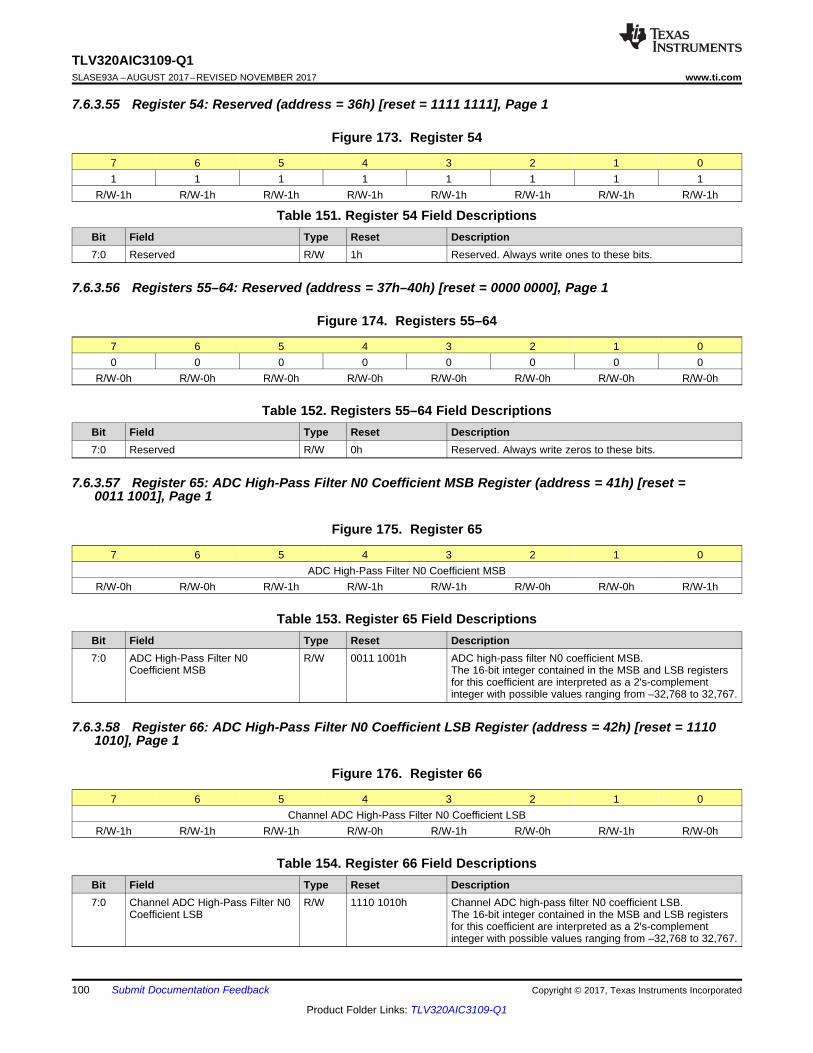
100
TLV320AIC3109-Q1SLASE93A –AUGUST 2017–REVISED NOVEMBER 2017 www.ti.com
Product Folder Links: TLV320AIC3109-Q1
Submit Documentation Feedback Copyright © 2017, Texas Instruments Incorporated
7.6.3.55 Register 54: Reserved (address = 36h) [reset = 1111 1111], Page 1
Figure 173. Register 54
7 6 5 4 3 2 1 01 1 1 1 1 1 1 1
R/W-1h R/W-1h R/W-1h R/W-1h R/W-1h R/W-1h R/W-1h R/W-1h
Table 151. Register 54 Field DescriptionsBit Field Type Reset Description7:0 Reserved R/W 1h Reserved. Always write ones to these bits.
7.6.3.56 Registers 55–64: Reserved (address = 37h–40h) [reset = 0000 0000], Page 1
Figure 174. Registers 55–64
7 6 5 4 3 2 1 00 0 0 0 0 0 0 0
R/W-0h R/W-0h R/W-0h R/W-0h R/W-0h R/W-0h R/W-0h R/W-0h
Table 152. Registers 55–64 Field DescriptionsBit Field Type Reset Description7:0 Reserved R/W 0h Reserved. Always write zeros to these bits.
7.6.3.57 Register 65: ADC High-Pass Filter N0 Coefficient MSB Register (address = 41h) [reset =0011 1001], Page 1
Figure 175. Register 65
7 6 5 4 3 2 1 0ADC High-Pass Filter N0 Coefficient MSB
R/W-0h R/W-0h R/W-1h R/W-1h R/W-1h R/W-0h R/W-0h R/W-1h
Table 153. Register 65 Field DescriptionsBit Field Type Reset Description7:0 ADC High-Pass Filter N0
Coefficient MSBR/W 0011 1001h ADC high-pass filter N0 coefficient MSB.
The 16-bit integer contained in the MSB and LSB registersfor this coefficient are interpreted as a 2's-complementinteger with possible values ranging from –32,768 to 32,767.
7.6.3.58 Register 66: ADC High-Pass Filter N0 Coefficient LSB Register (address = 42h) [reset = 11101010], Page 1
Figure 176. Register 66
7 6 5 4 3 2 1 0Channel ADC High-Pass Filter N0 Coefficient LSB
R/W-1h R/W-1h R/W-1h R/W-0h R/W-1h R/W-0h R/W-1h R/W-0h
Table 154. Register 66 Field DescriptionsBit Field Type Reset Description7:0 Channel ADC High-Pass Filter N0
Coefficient LSBR/W 1110 1010h Channel ADC high-pass filter N0 coefficient LSB.
The 16-bit integer contained in the MSB and LSB registersfor this coefficient are interpreted as a 2's-complementinteger with possible values ranging from –32,768 to 32,767.
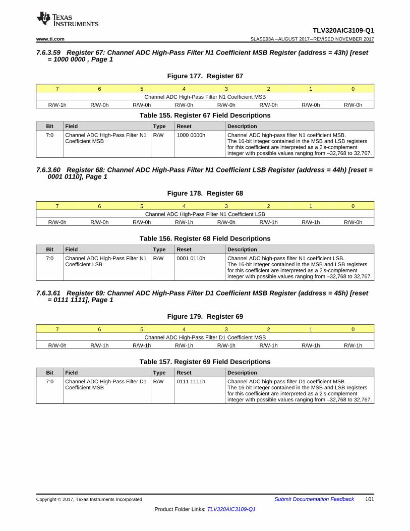
101
TLV320AIC3109-Q1www.ti.com SLASE93A –AUGUST 2017–REVISED NOVEMBER 2017
Product Folder Links: TLV320AIC3109-Q1
Submit Documentation FeedbackCopyright © 2017, Texas Instruments Incorporated
7.6.3.59 Register 67: Channel ADC High-Pass Filter N1 Coefficient MSB Register (address = 43h) [reset= 1000 0000 , Page 1
Figure 177. Register 67
7 6 5 4 3 2 1 0Channel ADC High-Pass Filter N1 Coefficient MSB
R/W-1h R/W-0h R/W-0h R/W-0h R/W-0h R/W-0h R/W-0h R/W-0h
Table 155. Register 67 Field DescriptionsBit Field Type Reset Description7:0 Channel ADC High-Pass Filter N1
Coefficient MSBR/W 1000 0000h Channel ADC high-pass filter N1 coefficient MSB.
The 16-bit integer contained in the MSB and LSB registersfor this coefficient are interpreted as a 2's-complementinteger with possible values ranging from –32,768 to 32,767.
7.6.3.60 Register 68: Channel ADC High-Pass Filter N1 Coefficient LSB Register (address = 44h) [reset =0001 0110], Page 1
Figure 178. Register 68
7 6 5 4 3 2 1 0Channel ADC High-Pass Filter N1 Coefficient LSB
R/W-0h R/W-0h R/W-0h R/W-1h R/W-0h R/W-1h R/W-1h R/W-0h
Table 156. Register 68 Field DescriptionsBit Field Type Reset Description7:0 Channel ADC High-Pass Filter N1
Coefficient LSBR/W 0001 0110h Channel ADC high-pass filter N1 coefficient LSB.
The 16-bit integer contained in the MSB and LSB registersfor this coefficient are interpreted as a 2's-complementinteger with possible values ranging from –32,768 to 32,767.
7.6.3.61 Register 69: Channel ADC High-Pass Filter D1 Coefficient MSB Register (address = 45h) [reset= 0111 1111], Page 1
Figure 179. Register 69
7 6 5 4 3 2 1 0Channel ADC High-Pass Filter D1 Coefficient MSB
R/W-0h R/W-1h R/W-1h R/W-1h R/W-1h R/W-1h R/W-1h R/W-1h
Table 157. Register 69 Field DescriptionsBit Field Type Reset Description7:0 Channel ADC High-Pass Filter D1
Coefficient MSBR/W 0111 1111h Channel ADC high-pass filter D1 coefficient MSB.
The 16-bit integer contained in the MSB and LSB registersfor this coefficient are interpreted as a 2's-complementinteger with possible values ranging from –32,768 to 32,767.

102
TLV320AIC3109-Q1SLASE93A –AUGUST 2017–REVISED NOVEMBER 2017 www.ti.com
Product Folder Links: TLV320AIC3109-Q1
Submit Documentation Feedback Copyright © 2017, Texas Instruments Incorporated
7.6.3.62 Register 70: Channel ADC High-Pass Filter D1 Coefficient LSB Register (address = 46h) [reset =1101 0101], Page 1
Figure 180. Register 70
7 6 5 4 3 2 1 0Channel ADC High-Pass Filter D1 Coefficient LSB
R/W-1h R/W-1h R/W-0h R/W-1h R/W-0h R/W-1h R/W-0h R/W-1h
Table 158. Register 70 Field DescriptionsBit Field Type Reset Description7:0 Channel ADC High-Pass Filter D1
Coefficient LSBR/W 1101 0101h Channel ADC high-pass filter D1 coefficient LSB.
The 16-bit integer contained in the MSB and LSB registersfor this coefficient are interpreted as a 2's-complementinteger with possible values ranging from –32,768 to 32,767.
7.6.3.63 Register 71: Reserved (address = 47h) [reset = 0111 1111], Page 1
Figure 181. Register 71
7 6 5 4 3 2 1 00 1 1 1 1 1 1 1
R/W-0h R/W-1h R/W-1h R/W-1h R/W-1h R/W-1h R/W-1h R/W-1h
Table 159. Register 71 Field DescriptionsBit Field Type Reset Description7:0 Reserved R/W 0111 1111h Reserved. Always write 0111 1111 to these bits.
7.6.3.64 Register 72: Reserved (address = 48h) [reset = 1110 1010], Page 1
Figure 182. Register 72
7 6 5 4 3 2 1 01 1 1 0 1 0 1 0
R/W-1h R/W-1h R/W-1h R/W-0h R/W-1h R/W-0h R/W-1h R/W-0h
Table 160. Register 72 Field DescriptionsBit Field Type Reset Description7:0 Reserved R/W 1110 1010h Reserved. Always write 1110 1010 to these bits.
7.6.3.65 Register 73: Reserved (address = 49h) [reset = 1000 0000], Page 1
Figure 183. Register 73
7 6 5 4 3 2 1 01 0 0 0 0 0 0 0
R/W-1h R/W-0h R/W-0h R/W-0h R/W-0h R/W-0h R/W-0h R/W-0h
Table 161. Register 73 Field DescriptionsBit Field Type Reset Description7:0 Reserved R/W 1000 0000h Reserved. Always write 1000 0000 to these bits.
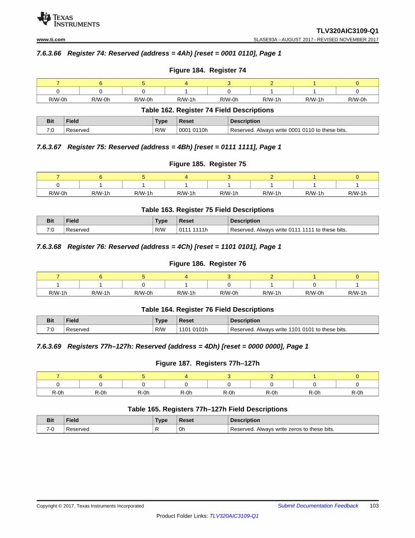
103
TLV320AIC3109-Q1www.ti.com SLASE93A –AUGUST 2017–REVISED NOVEMBER 2017
Product Folder Links: TLV320AIC3109-Q1
Submit Documentation FeedbackCopyright © 2017, Texas Instruments Incorporated
7.6.3.66 Register 74: Reserved (address = 4Ah) [reset = 0001 0110], Page 1
Figure 184. Register 74
7 6 5 4 3 2 1 00 0 0 1 0 1 1 0
R/W-0h R/W-0h R/W-0h R/W-1h R/W-0h R/W-1h R/W-1h R/W-0h
Table 162. Register 74 Field DescriptionsBit Field Type Reset Description7:0 Reserved R/W 0001 0110h Reserved. Always write 0001 0110 to these bits.
7.6.3.67 Register 75: Reserved (address = 4Bh) [reset = 0111 1111], Page 1
Figure 185. Register 75
7 6 5 4 3 2 1 00 1 1 1 1 1 1 1
R/W-0h R/W-1h R/W-1h R/W-1h R/W-1h R/W-1h R/W-1h R/W-1h
Table 163. Register 75 Field DescriptionsBit Field Type Reset Description7:0 Reserved R/W 0111 1111h Reserved. Always write 0111 1111 to these bits.
7.6.3.68 Register 76: Reserved (address = 4Ch) [reset = 1101 0101], Page 1
Figure 186. Register 76
7 6 5 4 3 2 1 01 1 0 1 0 1 0 1
R/W-1h R/W-1h R/W-0h R/W-1h R/W-0h R/W-1h R/W-0h R/W-1h
Table 164. Register 76 Field DescriptionsBit Field Type Reset Description7:0 Reserved R/W 1101 0101h Reserved. Always write 1101 0101 to these bits.
7.6.3.69 Registers 77h–127h: Reserved (address = 4Dh) [reset = 0000 0000], Page 1
Figure 187. Registers 77h–127h
7 6 5 4 3 2 1 00 0 0 0 0 0 0 0
R-0h R-0h R-0h R-0h R-0h R-0h R-0h R-0h
Table 165. Registers 77h–127h Field DescriptionsBit Field Type Reset Description7-0 Reserved R 0h Reserved. Always write zeros to these bits.
104
TLV320AIC3109-Q1SLASE93A –AUGUST 2017–REVISED NOVEMBER 2017 www.ti.com
Product Folder Links: TLV320AIC3109-Q1
Submit Documentation Feedback Copyright © 2017, Texas Instruments Incorporated
8 Application and Implementation
NOTEInformation in the following applications sections is not part of the TI componentspecification, and TI does not warrant its accuracy or completeness. TI’s customers areresponsible for determining suitability of components for their purposes. Customers shouldvalidate and test their design implementation to confirm system functionality.
8.1 Application InformationThe TLV320AIC3109-Q1 is a highly integrated low-power mono audio codec with integrated headphone and lineamplifiers. All features of the TLV320AIC3109-Q1 are accessed by programmable registers. An externalprocessor with I2C protocol is required to control the device. Good practice is to perform a hardware reset afterinitial power-up to ensure that all registers are in default states. Extensive register-based power control isincluded, enabling mono 48-kHz DAC playback as low as 14-mW from a 3.3-V analog supply, making the deviceideal for portable battery-powered audio applications.
8.2 Typical ApplicationGoverning bodies around the world have implemented specific legislation to require automotive companies toinstall emergency call (E-Call) systems in order to reduce emergency response times and thereby save lives. E-Call systems are activated during a collision or emergency situation and automatically facilitate a call toemergency services. The state of a vehicle after a collision is difficult to predict and can include a disconnectedbattery, trapped passengers, and a noisy environment. For this reason, the E-Call module must have its ownbattery power source and be able to sustain a hands-free call for at least ten minutes (depending on specificregional legislation). The TLV320AIC3109-Q1 as an audio codec and the TAS5411-Q1 as an audio amplifier areoptimal choices for an E-Call application because these devices offers low power consumption and still allow aloud and clear conversation with an emergency operator.

Wireless Module andI2C Control
IOVDD
RP RP
SC
L
SD
A
RE
SE
T
MC
LK
BC
LK
WC
LK
DO
UT
DIN
TI Device
1 k:
1 k:
0.1 PF
0.1 PF
MICBIAS
MIC1P/LINE1P
MIC1M/LINE1M
MIC2P/LINE2P
MIC2M/LINE2M
(OPTIONAL MIC/LINE)
HP
CO
M
HP
OU
T
(OPTIONAL HEADPHONE)
AVDD
DRVDD
DRVDD
IOVDD
DVDD
DVSS
AVSS
AVSS
DRVSS
RIG
HT
_LO
M
RIG
HT
_LO
P
LEF
T_L
OP
LEF
T_L
OM
TAS5411-Q1 OR SIMILAR
TAS5411-Q1 OR SIMILAR
ANALOG GROUND
AVDD
1 PF0.1 PF
1 PF0.1µF
1mF
0.1µF
ANALOG GROUND
IOVDD
DVDD 1 PF
0.1µF
0.1µF 1µF
DIGITAL GROUND
Copyright © 2017, Texas Instruments Incorporated
105
TLV320AIC3109-Q1www.ti.com SLASE93A –AUGUST 2017–REVISED NOVEMBER 2017
Product Folder Links: TLV320AIC3109-Q1
Submit Documentation FeedbackCopyright © 2017, Texas Instruments Incorporated
Typical Application (continued)
Figure 188. Typical Connections for Emergency Call System (E-Call)
8.2.1 Design RequirementsTable 166 shows the parameters used for this application.
Table 166. Design ParametersPARAMETER VALUE
AVDD, DRVDD 3.3 VIOVDD, DVDD 1.8 V
MCLK frequency 12.288 MHzBCLK frequency 3.072 MHz
WCLK frequency (sample rate) 48 KHzCurrent consumption (AVDD + DRVDD) 4.31 mACurrent consumption (DVDD + IOVDD) 2.45 mA
Total power consumption 20 mW
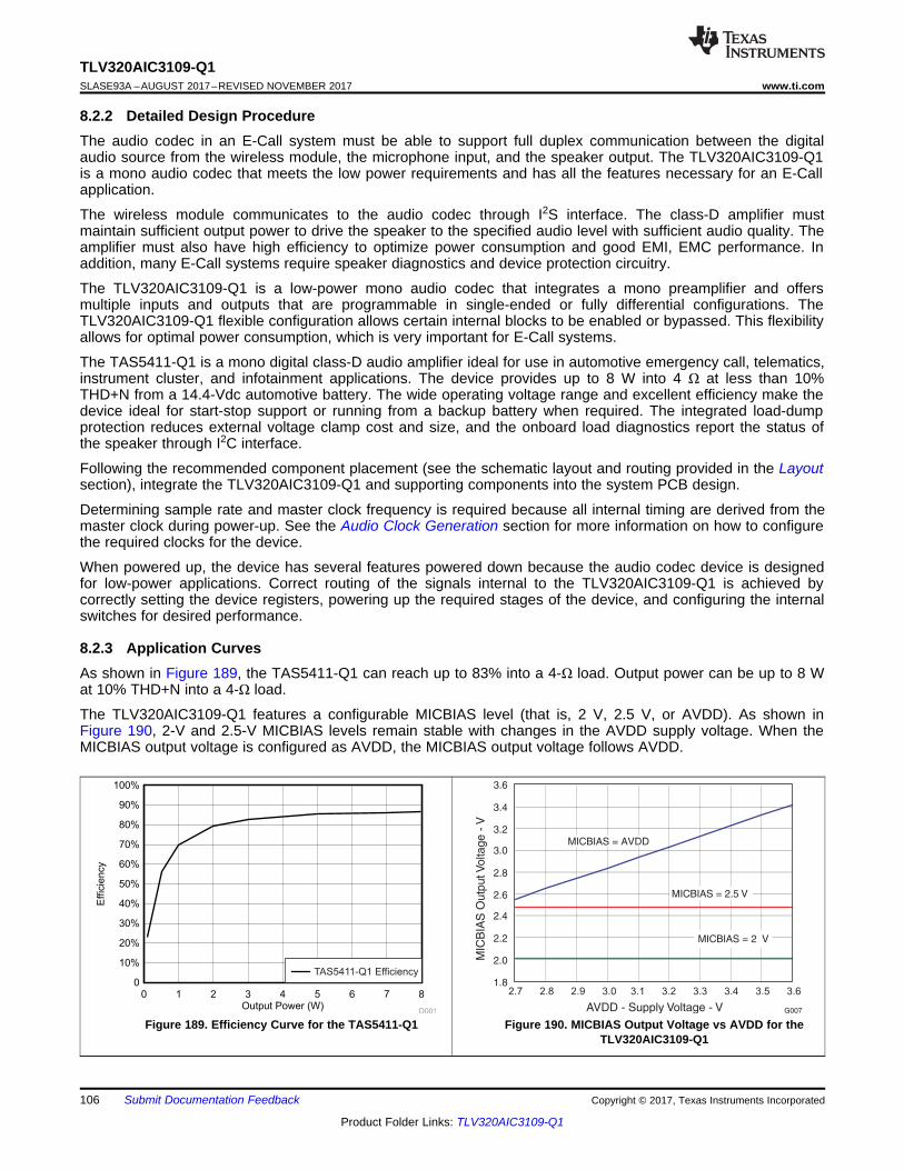
TAS5411-Q1 Efficiency1.8
2.0
2.2
2.4
2.6
2.8
3.0
3.2
3.4
3.6
AVDD - Supply Voltage - V
MIC
BIA
S O
utp
utV
oltage
-V
G007
MICBIAS = AVDD
MICBIAS = 2.5 V
MICBIAS = 2 V
2.7 2.8 2.9 3.0 3.1 3.2 3.3 3.4 3.5 3.6
106
TLV320AIC3109-Q1SLASE93A –AUGUST 2017–REVISED NOVEMBER 2017 www.ti.com
Product Folder Links: TLV320AIC3109-Q1
Submit Documentation Feedback Copyright © 2017, Texas Instruments Incorporated
8.2.2 Detailed Design ProcedureThe audio codec in an E-Call system must be able to support full duplex communication between the digitalaudio source from the wireless module, the microphone input, and the speaker output. The TLV320AIC3109-Q1is a mono audio codec that meets the low power requirements and has all the features necessary for an E-Callapplication.
The wireless module communicates to the audio codec through I2S interface. The class-D amplifier mustmaintain sufficient output power to drive the speaker to the specified audio level with sufficient audio quality. Theamplifier must also have high efficiency to optimize power consumption and good EMI, EMC performance. Inaddition, many E-Call systems require speaker diagnostics and device protection circuitry.
The TLV320AIC3109-Q1 is a low-power mono audio codec that integrates a mono preamplifier and offersmultiple inputs and outputs that are programmable in single-ended or fully differential configurations. TheTLV320AIC3109-Q1 flexible configuration allows certain internal blocks to be enabled or bypassed. This flexibilityallows for optimal power consumption, which is very important for E-Call systems.
The TAS5411-Q1 is a mono digital class-D audio amplifier ideal for use in automotive emergency call, telematics,instrument cluster, and infotainment applications. The device provides up to 8 W into 4 Ω at less than 10%THD+N from a 14.4-Vdc automotive battery. The wide operating voltage range and excellent efficiency make thedevice ideal for start-stop support or running from a backup battery when required. The integrated load-dumpprotection reduces external voltage clamp cost and size, and the onboard load diagnostics report the status ofthe speaker through I2C interface.
Following the recommended component placement (see the schematic layout and routing provided in the Layoutsection), integrate the TLV320AIC3109-Q1 and supporting components into the system PCB design.
Determining sample rate and master clock frequency is required because all internal timing are derived from themaster clock during power-up. See the Audio Clock Generation section for more information on how to configurethe required clocks for the device.
When powered up, the device has several features powered down because the audio codec device is designedfor low-power applications. Correct routing of the signals internal to the TLV320AIC3109-Q1 is achieved bycorrectly setting the device registers, powering up the required stages of the device, and configuring the internalswitches for desired performance.
8.2.3 Application CurvesAs shown in Figure 189, the TAS5411-Q1 can reach up to 83% into a 4-Ω load. Output power can be up to 8 Wat 10% THD+N into a 4-Ω load.
The TLV320AIC3109-Q1 features a configurable MICBIAS level (that is, 2 V, 2.5 V, or AVDD). As shown inFigure 190, 2-V and 2.5-V MICBIAS levels remain stable with changes in the AVDD supply voltage. When theMICBIAS output voltage is configured as AVDD, the MICBIAS output voltage follows AVDD.
Figure 189. Efficiency Curve for the TAS5411-Q1 Figure 190. MICBIAS Output Voltage vs AVDD for theTLV320AIC3109-Q1

IOVDD
AVDD, DRVDD
DVDD
t1
t 2
t3
107
TLV320AIC3109-Q1www.ti.com SLASE93A –AUGUST 2017–REVISED NOVEMBER 2017
Product Folder Links: TLV320AIC3109-Q1
Submit Documentation FeedbackCopyright © 2017, Texas Instruments Incorporated
9 Power Supply RecommendationsThe TLV320AIC3109-Q1 is designed to be extremely tolerant of power-supply sequencing. However, in somerare instances, unexpected conditions can be attributed to power-supply sequencing. The following sequenceprovides the most robust operation.
Power-up IOVDD first. Power-up the analog supplies, which includes AVDD and DRVDD, second. Power-up thedigital supply DVDD last. Keep RESET low until all supplies are stable. The analog supplies must be greaterthan or equal to DVDD at all times. Figure 191 and Table 167 detail the preferred power-supply sequence.
Figure 191. TLV320AIC3109-Q1 Power-Supply Sequencing
Table 167. TLV320AIC3109-Q1 Power-SupplySequencing
MIN MAX UNITt1 IOVDD to AVDD, DRVDD 0 mst2 AVDD to DVDD 0 5 mst3 IOVDD, to DVDD 0 ms
10 Layout
10.1 Layout GuidelinesPrinted circuit board (PCB) design is made considering the application, and the review is specific for each systemrequirements. However, general considerations can optimize the system performance:• Connect the TLV320AIC3109-Q1 thermal pad to the analog output driver ground• Separate the analog and digital grounds to prevent possible digital noise from affecting the analog
performance of the board• The TLV320AIC3109-Q1 requires the decoupling capacitors to be placed as close as possible to the device
power-supply terminals• If possible, route the differential audio signals differentially on the PCB to obtain better noise immunity
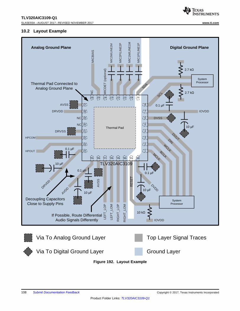
Thermal Pad Connected toAnalog Ground Plane
Thermal Pad
124
223
322
421
520
619
718
817
9
32
10
31
11
30
12
29
13
28
14
27
15
26
16
25
SystemProcessor
0.1 F
10 F
10 F
0.1 F
Decoupling CapacitorsClose to Supply Pins
If Possible, Route Differential Audio Signals Differently
10 F
0.1 F
SystemProcessor
10 k
10 F
2.7 k
Analog Ground Plane Digital Ground Plane
2.7 k
0.1 F
Via To Analog Ground Layer
Via To Digital Ground Layer
Top Layer Signal Traces
Ground Layer
MIC
1P/L
INE
1P
MIC
1M/L
INE
1M
MIC
2P/L
INE
2P
MIC
2M/L
INE
2M
MIC
DE
T (
optio
nal)
MIC
BIA
S
RE
SE
T
RIG
HT
_LO
M
RIG
HT
_LO
P
LEF
T_L
OM
LEF
T_L
OP
AV
SS
DVDD
HPOUT
HPCOM
DRVSS
NC
NC
DRVDD
AVSS
DRVDD
IOVDD
MCLK
BCLK
SDA
NC
WCLK
DIN
DOUT
DVSS
IOVDD
SCL
AVDD
TLV320AIC3109
108
TLV320AIC3109-Q1SLASE93A –AUGUST 2017–REVISED NOVEMBER 2017 www.ti.com
Product Folder Links: TLV320AIC3109-Q1
Submit Documentation Feedback Copyright © 2017, Texas Instruments Incorporated
10.2 Layout Example
Figure 192. Layout Example

109
TLV320AIC3109-Q1www.ti.com SLASE93A –AUGUST 2017–REVISED NOVEMBER 2017
Product Folder Links: TLV320AIC3109-Q1
Submit Documentation FeedbackCopyright © 2017, Texas Instruments Incorporated
11 Device and Documentation Support
11.1 Documentation Support
11.1.1 Related DocumentationFor related documentation see the following:
TAS5411-Q1 8-W Mono Automotive Class-D Audio Amplifier With Load Dump and I2C Diagnostics
11.2 Receiving Notification of Documentation UpdatesTo receive notification of documentation updates, navigate to the device product folder on ti.com. In the upperright corner, click on Alert me to register and receive a weekly digest of any product information that haschanged. For change details, review the revision history included in any revised document.
11.3 Community ResourcesThe following links connect to TI community resources. Linked contents are provided "AS IS" by the respectivecontributors. They do not constitute TI specifications and do not necessarily reflect TI's views; see TI's Terms ofUse.
TI E2E™ Online Community TI's Engineer-to-Engineer (E2E) Community. Created to foster collaborationamong engineers. At e2e.ti.com, you can ask questions, share knowledge, explore ideas and helpsolve problems with fellow engineers.
Design Support TI's Design Support Quickly find helpful E2E forums along with design support tools andcontact information for technical support.
11.4 TrademarksE2E is a trademark of Texas Instruments.All other trademarks are the property of their respective owners.
11.5 Electrostatic Discharge CautionThis integrated circuit can be damaged by ESD. Texas Instruments recommends that all integrated circuits be handled withappropriate precautions. Failure to observe proper handling and installation procedures can cause damage.
ESD damage can range from subtle performance degradation to complete device failure. Precision integrated circuits may be moresusceptible to damage because very small parametric changes could cause the device not to meet its published specifications.
11.6 GlossarySLYZ022 — TI Glossary.
This glossary lists and explains terms, acronyms, and definitions.
12 Mechanical, Packaging, and Orderable InformationThe following pages include mechanical, packaging, and orderable information. This information is the mostcurrent data available for the designated devices. This data is subject to change without notice and revision ofthis document. For browser-based versions of this data sheet, refer to the left-hand navigation.
PACKAGE OPTION ADDENDUM
www.ti.com 20-Feb-2018
Addendum-Page 1
PACKAGING INFORMATION
Orderable Device Status(1)
Package Type PackageDrawing
Pins PackageQty
Eco Plan(2)
Lead/Ball Finish(6)
MSL Peak Temp(3)
Op Temp (°C) Device Marking(4/5)
Samples
6PAIC3109TRHBRQ1 ACTIVE VQFN RHB 32 3000 Green (RoHS& no Sb/Br)
CU NIPDAU Level-3-260C-168 HR -40 to 105 3109T
6PAIC3109TWRHMRQ1 ACTIVE VQFN RHM 32 3000 Green (RoHS& no Sb/Br)
CU NIPDAUAG Level-3-260C-168 HR -40 to 105 3109TW
(1) The marketing status values are defined as follows:ACTIVE: Product device recommended for new designs.LIFEBUY: TI has announced that the device will be discontinued, and a lifetime-buy period is in effect.NRND: Not recommended for new designs. Device is in production to support existing customers, but TI does not recommend using this part in a new design.PREVIEW: Device has been announced but is not in production. Samples may or may not be available.OBSOLETE: TI has discontinued the production of the device.
(2) RoHS: TI defines "RoHS" to mean semiconductor products that are compliant with the current EU RoHS requirements for all 10 RoHS substances, including the requirement that RoHS substancedo not exceed 0.1% by weight in homogeneous materials. Where designed to be soldered at high temperatures, "RoHS" products are suitable for use in specified lead-free processes. TI mayreference these types of products as "Pb-Free".RoHS Exempt: TI defines "RoHS Exempt" to mean products that contain lead but are compliant with EU RoHS pursuant to a specific EU RoHS exemption.Green: TI defines "Green" to mean the content of Chlorine (Cl) and Bromine (Br) based flame retardants meet JS709B low halogen requirements of <=1000ppm threshold. Antimony trioxide basedflame retardants must also meet the <=1000ppm threshold requirement.
(3) MSL, Peak Temp. - The Moisture Sensitivity Level rating according to the JEDEC industry standard classifications, and peak solder temperature.
(4) There may be additional marking, which relates to the logo, the lot trace code information, or the environmental category on the device.
(5) Multiple Device Markings will be inside parentheses. Only one Device Marking contained in parentheses and separated by a "~" will appear on a device. If a line is indented then it is a continuationof the previous line and the two combined represent the entire Device Marking for that device.
(6) Lead/Ball Finish - Orderable Devices may have multiple material finish options. Finish options are separated by a vertical ruled line. Lead/Ball Finish values may wrap to two lines if the finishvalue exceeds the maximum column width.
Important Information and Disclaimer:The information provided on this page represents TI's knowledge and belief as of the date that it is provided. TI bases its knowledge and belief on informationprovided by third parties, and makes no representation or warranty as to the accuracy of such information. Efforts are underway to better integrate information from third parties. TI has taken andcontinues to take reasonable steps to provide representative and accurate information but may not have conducted destructive testing or chemical analysis on incoming materials and chemicals.TI and TI suppliers consider certain information to be proprietary, and thus CAS numbers and other limited information may not be available for release.
In no event shall TI's liability arising out of such information exceed the total purchase price of the TI part(s) at issue in this document sold by TI to Customer on an annual basis.

PACKAGE OPTION ADDENDUM
www.ti.com 20-Feb-2018
Addendum-Page 2
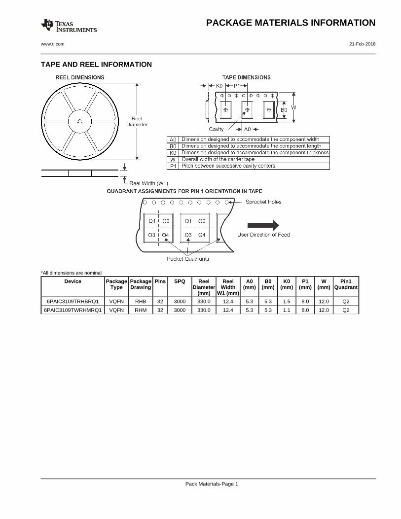
TAPE AND REEL INFORMATION
*All dimensions are nominal
Device PackageType
PackageDrawing
Pins SPQ ReelDiameter
(mm)
ReelWidth
W1 (mm)
A0(mm)
B0(mm)
K0(mm)
P1(mm)
W(mm)
Pin1Quadrant
6PAIC3109TRHBRQ1 VQFN RHB 32 3000 330.0 12.4 5.3 5.3 1.5 8.0 12.0 Q2
6PAIC3109TWRHMRQ1 VQFN RHM 32 3000 330.0 12.4 5.3 5.3 1.1 8.0 12.0 Q2
PACKAGE MATERIALS INFORMATION
www.ti.com 21-Feb-2018
Pack Materials-Page 1

*All dimensions are nominal
Device Package Type Package Drawing Pins SPQ Length (mm) Width (mm) Height (mm)
6PAIC3109TRHBRQ1 VQFN RHB 32 3000 367.0 367.0 35.0
6PAIC3109TWRHMRQ1 VQFN RHM 32 3000 367.0 367.0 35.0
PACKAGE MATERIALS INFORMATION
www.ti.com 21-Feb-2018
Pack Materials-Page 2
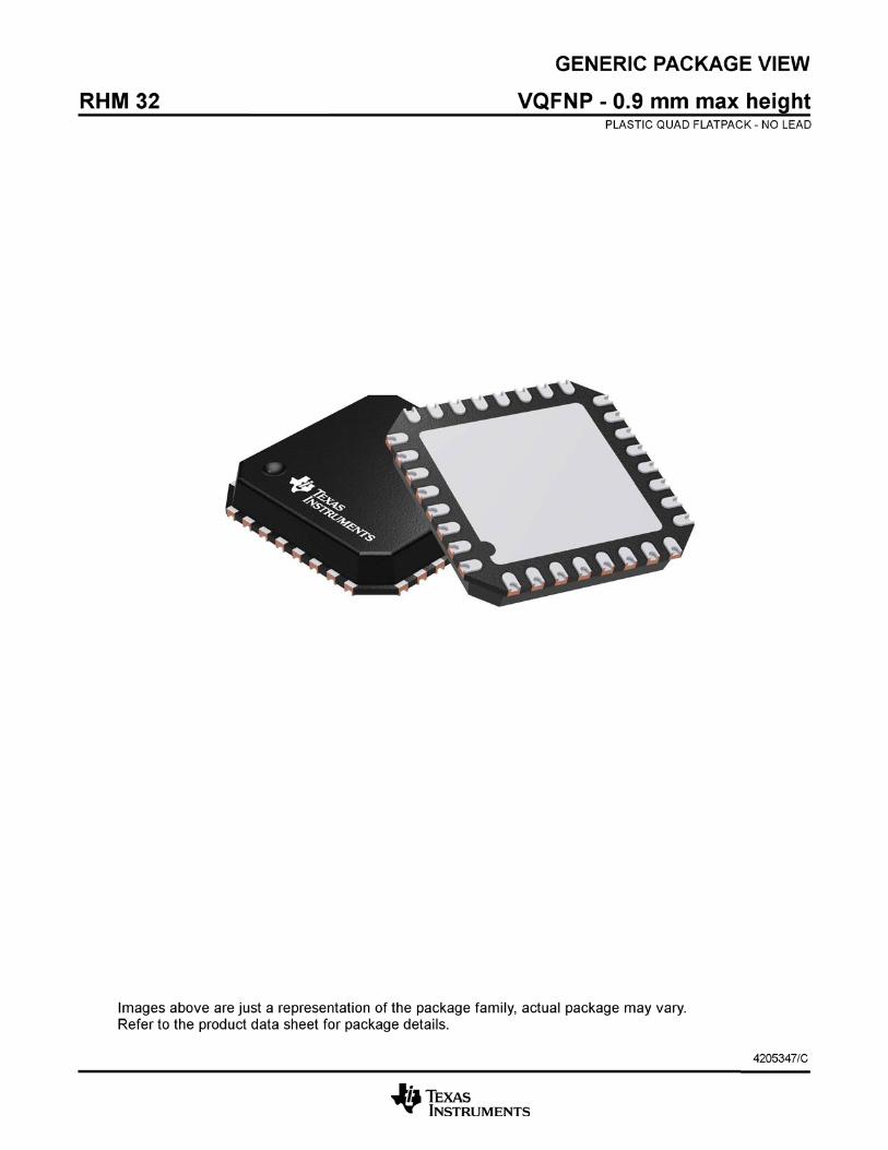
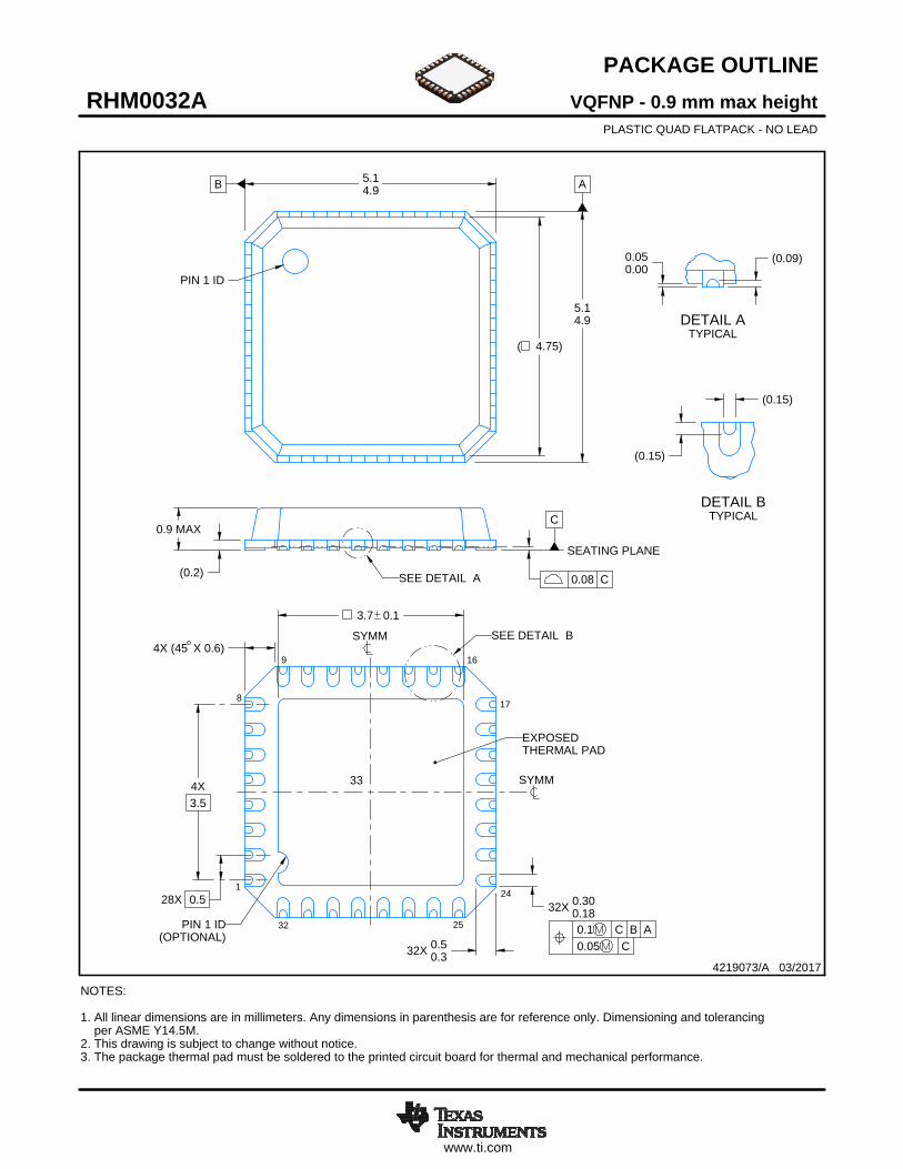
www.ti.com
PACKAGE OUTLINE
C
PIN 1 ID
3.7 0.1
0.9 MAX
4X3.5
32X 0.300.18
28X 0.5
4X (45 X 0.6)
32X 0.50.3
0.050.00
( 4.75)
(0.15)
(0.09)
B 5.14.9 A
5.14.9
(0.2)
(0.15)
4219073/A 03/2017
VQFNP - 0.9 mm max heightRHM0032APLASTIC QUAD FLATPACK - NO LEAD
NOTES: 1. All linear dimensions are in millimeters. Any dimensions in parenthesis are for reference only. Dimensioning and tolerancing per ASME Y14.5M. 2. This drawing is subject to change without notice. 3. The package thermal pad must be soldered to the printed circuit board for thermal and mechanical performance.
24
17
169
8
1
32 25 0.1 C B A0.05 C
PIN 1 ID(OPTIONAL)
SYMM
SYMM SEE DETAIL B
EXPOSEDTHERMAL PAD
33
0.08 C
SEATING PLANE
SEE DETAIL A
SCALE 3.000
DETAIL ASCALE 20.000
DETAIL ATYPICAL
DETAIL BSCALE 20.000DETAIL B
TYPICAL

www.ti.com
EXAMPLE BOARD LAYOUT
0.05 MAXALL AROUND
0.05 MINALL AROUND
32X (0.25)
32X (0.6)
28X (0.5)
(4.8)
(4.8)4X
(1.26)
4X (1.26)
( 0.2) VIATYP
(R0.05)TYP
( 3.7)
4X (0.97)
4X(0.97)
4219073/A 03/2017
VQFNP - 0.9 mm max heightRHM0032APLASTIC QUAD FLATPACK - NO LEAD
SYMM
SYMM
LAND PATTERN EXAMPLEEXPOSED METAL SHOWN
SCALE:15X
1
8
9 16
17
24
2532
33
NOTES: (continued) 4. This package is designed to be soldered to a thermal pad on the board. For more information, see Texas Instruments literature number SLUA271 (www.ti.com/lit/slua271).5. Vias are optional depending on application, refer to device data sheet. If any vias are implemented, refer to their locations shown on this view. It is recommended that vias under paste be filled, plugged or tented.
METAL
SOLDER MASKOPENING
SOLDER MASK DETAILS
NON SOLDER MASKDEFINED
(PREFERRED)
EXPOSED METAL
SOLDER MASKOPENING
METAL UNDERSOLDER MASK
SOLDER MASKDEFINED
EXPOSED METAL

www.ti.com
EXAMPLE STENCIL DESIGN
(4.8)
32X (0.6)
32X (0.25)
28X (0.5)
4X ( 1.06)
(1.26 TYP)
(4.8)
(1.26)TYP
(R0.05)TYP
4219073/A 03/2017
VQFNP - 0.9 mm max heightRHM0032APLASTIC QUAD FLATPACK - NO LEAD
NOTES: (continued) 6. Laser cutting apertures with trapezoidal walls and rounded corners may offer better paste release. IPC-7525 may have alternate design recommendations.
METALTYP
SOLDER PASTE EXAMPLEBASED ON 0.125 mm THICK STENCIL
EXPOSED PAD 33:
74% PRINTED SOLDER COVERAGE BY AREA UNDER PACKAGESCALE:18X
SYMM
SYMM
1
8
9 16
17
24
2532
33
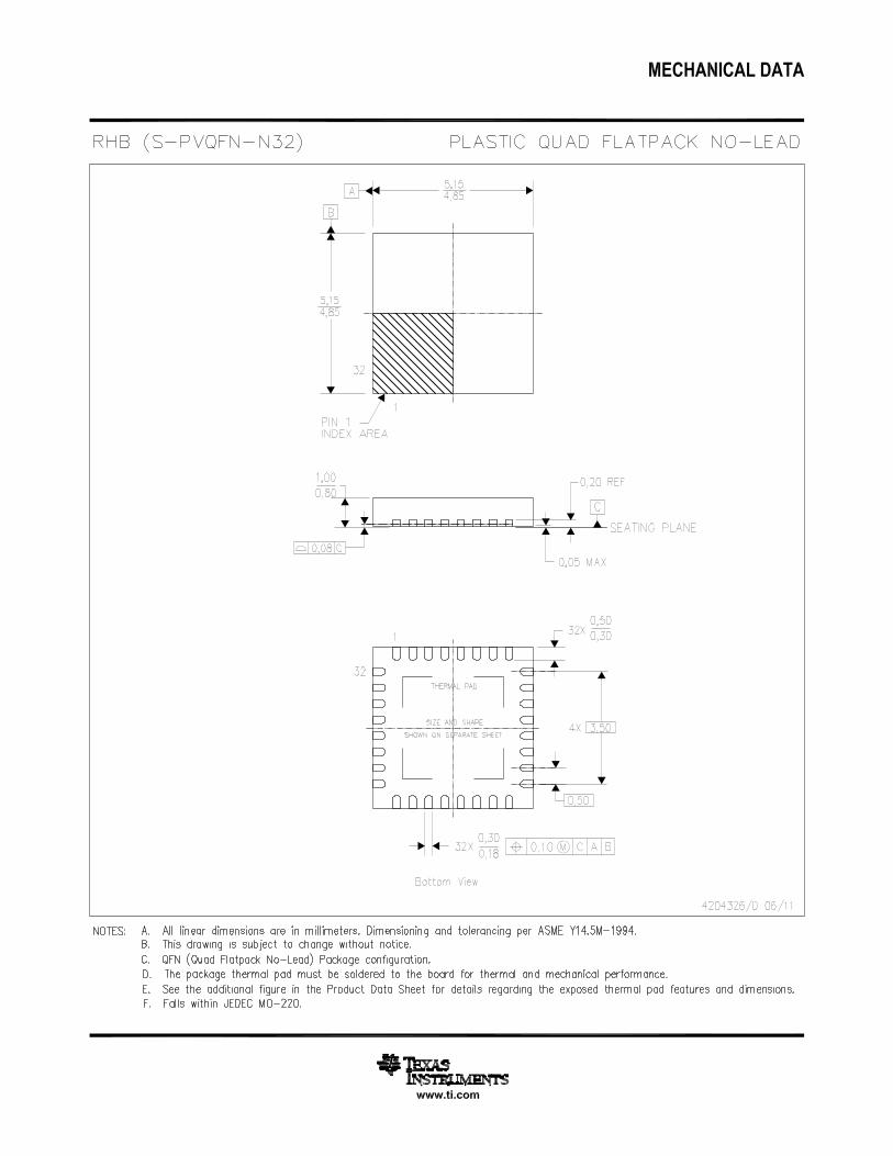
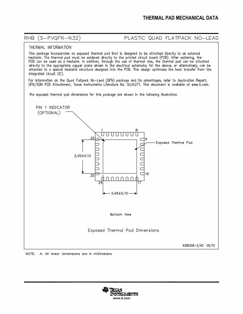


IMPORTANT NOTICE
Texas Instruments Incorporated (TI) reserves the right to make corrections, enhancements, improvements and other changes to itssemiconductor products and services per JESD46, latest issue, and to discontinue any product or service per JESD48, latest issue. Buyersshould obtain the latest relevant information before placing orders and should verify that such information is current and complete.TI’s published terms of sale for semiconductor products (http://www.ti.com/sc/docs/stdterms.htm) apply to the sale of packaged integratedcircuit products that TI has qualified and released to market. Additional terms may apply to the use or sale of other types of TI products andservices.Reproduction of significant portions of TI information in TI data sheets is permissible only if reproduction is without alteration and isaccompanied by all associated warranties, conditions, limitations, and notices. TI is not responsible or liable for such reproduceddocumentation. Information of third parties may be subject to additional restrictions. Resale of TI products or services with statementsdifferent from or beyond the parameters stated by TI for that product or service voids all express and any implied warranties for theassociated TI product or service and is an unfair and deceptive business practice. TI is not responsible or liable for any such statements.Buyers and others who are developing systems that incorporate TI products (collectively, “Designers”) understand and agree that Designersremain responsible for using their independent analysis, evaluation and judgment in designing their applications and that Designers havefull and exclusive responsibility to assure the safety of Designers' applications and compliance of their applications (and of all TI productsused in or for Designers’ applications) with all applicable regulations, laws and other applicable requirements. Designer represents that, withrespect to their applications, Designer has all the necessary expertise to create and implement safeguards that (1) anticipate dangerousconsequences of failures, (2) monitor failures and their consequences, and (3) lessen the likelihood of failures that might cause harm andtake appropriate actions. Designer agrees that prior to using or distributing any applications that include TI products, Designer willthoroughly test such applications and the functionality of such TI products as used in such applications.TI’s provision of technical, application or other design advice, quality characterization, reliability data or other services or information,including, but not limited to, reference designs and materials relating to evaluation modules, (collectively, “TI Resources”) are intended toassist designers who are developing applications that incorporate TI products; by downloading, accessing or using TI Resources in anyway, Designer (individually or, if Designer is acting on behalf of a company, Designer’s company) agrees to use any particular TI Resourcesolely for this purpose and subject to the terms of this Notice.TI’s provision of TI Resources does not expand or otherwise alter TI’s applicable published warranties or warranty disclaimers for TIproducts, and no additional obligations or liabilities arise from TI providing such TI Resources. TI reserves the right to make corrections,enhancements, improvements and other changes to its TI Resources. TI has not conducted any testing other than that specificallydescribed in the published documentation for a particular TI Resource.Designer is authorized to use, copy and modify any individual TI Resource only in connection with the development of applications thatinclude the TI product(s) identified in such TI Resource. NO OTHER LICENSE, EXPRESS OR IMPLIED, BY ESTOPPEL OR OTHERWISETO ANY OTHER TI INTELLECTUAL PROPERTY RIGHT, AND NO LICENSE TO ANY TECHNOLOGY OR INTELLECTUAL PROPERTYRIGHT OF TI OR ANY THIRD PARTY IS GRANTED HEREIN, including but not limited to any patent right, copyright, mask work right, orother intellectual property right relating to any combination, machine, or process in which TI products or services are used. Informationregarding or referencing third-party products or services does not constitute a license to use such products or services, or a warranty orendorsement thereof. Use of TI Resources may require a license from a third party under the patents or other intellectual property of thethird party, or a license from TI under the patents or other intellectual property of TI.TI RESOURCES ARE PROVIDED “AS IS” AND WITH ALL FAULTS. TI DISCLAIMS ALL OTHER WARRANTIES ORREPRESENTATIONS, EXPRESS OR IMPLIED, REGARDING RESOURCES OR USE THEREOF, INCLUDING BUT NOT LIMITED TOACCURACY OR COMPLETENESS, TITLE, ANY EPIDEMIC FAILURE WARRANTY AND ANY IMPLIED WARRANTIES OFMERCHANTABILITY, FITNESS FOR A PARTICULAR PURPOSE, AND NON-INFRINGEMENT OF ANY THIRD PARTY INTELLECTUALPROPERTY RIGHTS. TI SHALL NOT BE LIABLE FOR AND SHALL NOT DEFEND OR INDEMNIFY DESIGNER AGAINST ANY CLAIM,INCLUDING BUT NOT LIMITED TO ANY INFRINGEMENT CLAIM THAT RELATES TO OR IS BASED ON ANY COMBINATION OFPRODUCTS EVEN IF DESCRIBED IN TI RESOURCES OR OTHERWISE. IN NO EVENT SHALL TI BE LIABLE FOR ANY ACTUAL,DIRECT, SPECIAL, COLLATERAL, INDIRECT, PUNITIVE, INCIDENTAL, CONSEQUENTIAL OR EXEMPLARY DAMAGES INCONNECTION WITH OR ARISING OUT OF TI RESOURCES OR USE THEREOF, AND REGARDLESS OF WHETHER TI HAS BEENADVISED OF THE POSSIBILITY OF SUCH DAMAGES.Unless TI has explicitly designated an individual product as meeting the requirements of a particular industry standard (e.g., ISO/TS 16949and ISO 26262), TI is not responsible for any failure to meet such industry standard requirements.Where TI specifically promotes products as facilitating functional safety or as compliant with industry functional safety standards, suchproducts are intended to help enable customers to design and create their own applications that meet applicable functional safety standardsand requirements. Using products in an application does not by itself establish any safety features in the application. Designers mustensure compliance with safety-related requirements and standards applicable to their applications. Designer may not use any TI products inlife-critical medical equipment unless authorized officers of the parties have executed a special contract specifically governing such use.Life-critical medical equipment is medical equipment where failure of such equipment would cause serious bodily injury or death (e.g., lifesupport, pacemakers, defibrillators, heart pumps, neurostimulators, and implantables). Such equipment includes, without limitation, allmedical devices identified by the U.S. Food and Drug Administration as Class III devices and equivalent classifications outside the U.S.TI may expressly designate certain products as completing a particular qualification (e.g., Q100, Military Grade, or Enhanced Product).Designers agree that it has the necessary expertise to select the product with the appropriate qualification designation for their applicationsand that proper product selection is at Designers’ own risk. Designers are solely responsible for compliance with all legal and regulatoryrequirements in connection with such selection.Designer will fully indemnify TI and its representatives against any damages, costs, losses, and/or liabilities arising out of Designer’s non-compliance with the terms and provisions of this Notice.
Mailing Address: Texas Instruments, Post Office Box 655303, Dallas, Texas 75265Copyright © 2018, Texas Instruments Incorporated